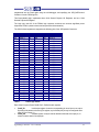
1
Signal Ranger mk3
Pro-Edition
User’s Manual
by
In association with
September 5 2011
1040, avenue Belvédère, suite 215
Québec (Québec) G1S 3G3 Canada
Tél.: (418) 686-0993 Fax: (418) 686-2043
1
FOREWORD _________________________________________________ 7
2
MAIN FEATURES _____________________________________________ 7
2.1
3
Boot Modes and Modes of Operation ______________________________________________ 7
TECHNICAL DATA ____________________________________________ 8
3.1
Power Supply __________________________________________________________________ 8
3.2
USB __________________________________________________________________________ 8
3.3
DSP __________________________________________________________________________ 8
3.4
FPGA ________________________________________________________________________ 8
3.5
Memory ______________________________________________________________________ 8
3.6
Ethernet Port __________________________________________________________________ 8
3.7
Expansion _____________________________________________________________________ 9
4
SOFTWARE __________________________________________________ 9
4.1
SignalRanger DDCI Interface _____________________________________________________ 9
4.2
Other Software Tools __________________________________________________________ 10
5
INSTALLATION AND TESTS ___________________________________ 11
5.1
Software Installation ___________________________________________________________ 11
5.1.1
LabVIEW Developer’s Package (SR3_DDCI_Library_Distribution.zip) _______________ 11
5.1.2
C/C++ Developer’s Package (SR3_Applications_Installer.exe) ______________________ 12
5.2
Hardware Installation __________________________________________________________ 12
5.3
What to Do In Case the Driver Installation Fails ____________________________________ 12
5.4
LED Indicator ________________________________________________________________ 13
5.5
Testing the Board______________________________________________________________ 13
6
6.1
HARDWARE DESCRIPTION ___________________________________ 14
Connector Map _______________________________________________________________ 14
6.2
Expansion Connector J7 ________________________________________________________ 15
6.2.1
J7 Pinout _________________________________________________________________ 15
Signal Ranger mk3 Pro - User’s Manual
3
6.3
Expansion Connector J4 ________________________________________________________ 16
6.3.1
J4 Pinout _________________________________________________________________ 16
6.4
System Frequencies ____________________________________________________________ 17
6.5
Peripheral Interfaces ___________________________________________________________ 17
6.5.1
Flash ROM _______________________________________________________________ 17
6.5.2
Ethernet Port ______________________________________________________________ 18
6.5.3
FPGA ____________________________________________________________________ 19
6.5.4
DDR2 RAM_______________________________________________________________ 22
6.6
Factory-Default FPGA Logic ____________________________________________________ 22
6.6.1
Hardware Details ___________________________________________________________ 24
6.6.2
Register Map ______________________________________________________________ 24
7
CODE DEVELOPMENT STRATEGY _____________________________ 24
8
MINI-DEBUGGER ____________________________________________ 25
8.1
9
Description of the User Interface _________________________________________________ 27
USB LABVIEW INTERFACE ____________________________________ 33
9.1
Preliminary Remarks __________________________________________________________ 33
9.2
Product Development Support ___________________________________________________ 33
9.3
Implicit Revision Information ___________________________________________________ 34
9.4
Suggested Firmware Upgrade Strategy ____________________________________________ 34
9.5
Development of a Product-Specific Application _____________________________________ 35
9.5.1
Opening the Target _________________________________________________________ 35
9.5.2
Execution Sequencing _______________________________________________________ 35
9.5.3
Loading and Executing Code Dynamically _______________________________________ 36
9.5.4
Firmware Storage and Locations Rules __________________________________________ 36
9.5.5
Building a LabVIEW Executable ______________________________________________ 38
9.5.6
Creating an Installer _________________________________________________________ 38
9.5.7
Required Support Firmware __________________________________________________ 38
9.6
USB Interface Vis _____________________________________________________________ 39
9.6.1
Core Interface VIs __________________________________________________________ 39
9.6.2
Flash Support VIs __________________________________________________________ 52
9.6.3
FPGA Support VIs__________________________________________________________ 56
10
ETHERNET LABVIEW INTERFACE ____________________________ 57
10.1 Preliminary Remarks __________________________________________________________ 57
10.1.1 Limitations of the Network Connection _________________________________________ 58
10.2 Opening the Target ____________________________________________________________ 58
10.2.1 Loading and Executing Code Dynamically _______________________________________ 59
Signal Ranger mk3 Pro - User’s Manual
4
10.3 Network Interface Vis __________________________________________________________ 59
10.3.1 Core Interface VIs __________________________________________________________ 59
10.3.2 Flash Support VIs __________________________________________________________ 64
11
C/C++ INTERFACE _________________________________________ 69
11.1
Execution Timing and Thread Management _______________________________________ 70
11.2
Calling Conventions ___________________________________________________________ 70
11.3
Building a Project Using Visual Studio ____________________________________________ 70
11.4 Exported USB Interface Functions _______________________________________________ 71
11.4.1 SR3_DLL_Open_Next_Avail_Board ___________________________________________ 71
11.4.2 SR3_DLL_Close_BoardNb ___________________________________________________ 72
11.4.3 SR3_DLL_Complete_DSP_Reset ______________________________________________ 72
11.4.4 SR3_DLL_WriteLeds _______________________________________________________ 73
11.4.5 SR3_DLL_Bulk_Move_Offset_U8 _____________________________________________ 73
11.4.6 SR3_DLL_User_Move_Offset_U8 _____________________________________________ 75
11.4.7 SR3_DLL_HPI_Move_Offset_U8 _____________________________________________ 77
11.4.8 SR3_DLL_LoadExec_User ___________________________________________________ 78
11.4.9 SR3_DLL_Load_User _______________________________________________________ 78
11.4.10
SR3_DLL_K_Exec _______________________________________________________ 79
11.4.11
SR3_DLL_Load_UserSymbols ______________________________________________ 80
11.4.12
SR3_DLL_Read_Error_Count ______________________________________________ 80
11.4.13
SR3_DLL_Clear_Error_Count ______________________________________________ 81
11.4.14
SR3_DLL_Flash_InitFlash _________________________________________________ 81
11.4.15
SR3_DLL_Flash_EraseFlash________________________________________________ 81
11.4.16
SR3_DLL_Flash_FlashMove_U8 ____________________________________________ 82
11.5 Exported Ethernet Interface Functions ____________________________________________ 83
11.5.1 SR3_DLL_Net_Open_Next_Avail_Board _______________________________________ 83
11.5.2 SR3_DLL_Net_Close_BoardNb _______________________________________________ 84
11.5.3 SR3_DLL_Net_Bulk_Move_Offset_U8 _________________________________________ 84
11.5.4 SR3_DLL_Net_K_Exec _____________________________________________________ 86
11.5.5 SR3_DLL_Net_Flash_InitFlash _______________________________________________ 86
11.5.6 SR3_DLL_Net_Flash_EraseFlash ______________________________________________ 87
11.5.7 SR3_DLL_Net_Flash_FlashMove_U8 __________________________________________ 87
12
DSP CODE DEVELOPMENT __________________________________ 88
12.1
Code Composer Studio Setup ____________________________________________________ 89
12.2
Project Requirements __________________________________________________________ 89
12.3
C-Code Requirements __________________________________________________________ 89
12.4
Assembly Requirements ________________________________________________________ 89
12.5 Build Options _________________________________________________________________ 90
12.5.1 Compiler _________________________________________________________________ 90
12.5.2 Linker ___________________________________________________________________ 90
12.6
Required Modules _____________________________________________________________ 90
Signal Ranger mk3 Pro - User’s Manual
5
12.6.1
Interrupt Vectors ___________________________________________________________ 90
12.7 Link Requirements ____________________________________________________________ 91
12.7.1 Memory Description File _____________________________________________________ 91
12.7.2 Stack Avoidance ___________________________________________________________ 91
12.8
Global Symbols _______________________________________________________________ 91
12.9
Preparing Code For “Self-Boot” _________________________________________________ 91
12.10
Under the Hood _____________________________________________________________ 92
12.10.1
Startup Process __________________________________________________________ 92
12.10.2
PC-Connection___________________________________________________________ 93
12.10.3
PC-Reset _______________________________________________________________ 93
12.10.4
Resources Used By The Kernel ______________________________________________ 93
12.10.5
USB Communications _____________________________________________________ 94
12.10.6
SR3 USB Communication Kernel ____________________________________________ 97
13
DSP SUPPORT CODE ______________________________________ 102
13.1 Flash Driver And Flash Programming Support Code _______________________________ 102
13.1.1 Overview of the flash driver _________________________________________________ 102
13.1.2 Used Resources ___________________________________________________________ 103
13.1.3 Setup of the Driver ________________________________________________________ 103
13.1.4 Data Structures ___________________________________________________________ 104
13.1.5 User Functions ____________________________________________________________ 105
13.2 Ethernet Support Code ________________________________________________________ 108
13.2.1 Operation Of The Net_Kernel ________________________________________________ 108
13.2.2 Resources Used By The Net_Kernel ___________________________________________ 110
Signal Ranger mk3 Pro - User’s Manual
6
1
Foreword
Beginning with the original Signal_Ranger series of DSP boards we adopted a policy of providing the
user with all the information necessary to operate our DSP boards, but also to understand their
operation to the finest possible detail. For instance we provide all the board schematics; we explain the
operation of the DSP kernels in detail… etc. In contrast with competing products this approach results
in a larger more detailed documentation that may give the impression of an overly complex system. Our
systems, tools and architectures are in fact easier to use than many competing products. Through the
years we have learned that many of our customers, some of them OEMs, appreciate this level of detail
and transparency in our documentation. Therefore we have decided to continue with this policy, and we
hope that you will take the time to go through the documentation to understand what our tools and
architectures can bring to your developments.
2
Main Features
SignalRanger_mk3_Pro is a fixed point DSP board featuring a TMS320C6424 DSP running at 590
MHz, a 400 kgates Spartan 3 FPGA running at 150 MHz, an Ethernet interface and a high-speed USB
2 interface, providing fast communications to the board. The USB Windows driver allows the
connection of any number of boards to a PC.
The DSP board may be used while connected to a PC, providing a means of exchanging data and
control between the PC and DSP in real-time. It may also be used in stand-alone mode, executing
embedded DSP code.
There are no ADCs and DACs on-board, but several add-on analog-IO cards, such as
SR2_Analog_810 can be added to the board. This allows Signal_Ranger_mk3_Pro to be used in highperformance control applications.
Given its flexible logic, its programmability and the fact that it can work as a stand-alone board, the
SignalRanger_mk3_Pro board may be used in many applications:
•
•
•
Multi-channel control.
Measurement and Instrumentation.
DSP software development.
2.1 Boot Modes and Modes of Operation
SignalRanger_mk3_Pro includes a 32MB Flash ROM, from which the DSP can boot.
There are two ways the DSP can boot:
•
•
Stand-Alone Boot:
At Power-Up, if firmware is present in Flash, it is loaded and
executed. By pre-programming the Flash memory with DSP code, the board can work in standalone mode, executing an embedded DSP application directly from power-up.
PC Boot:
When the board is connected to a PC, the PC can force the DSP to
reboot. In this mode, the PC can force the reloading of new DSP code. This mode may be used to
“take control” of the DSP at any time. In particular, it may be used to reprogram the Flash memory
in a completely transparent manner.
Even after the DSP board has booted in stand-alone mode, a PC can be connected at any time to
read/write DSP memory without interrupting the already executing DSP code. This behaviour provides
real-time visibility into, and control over the already executing embedded DSP code.
The flexibility offered by these boot modes support the following modes of operation:
Signal Ranger mk3 Pro - User’s Manual
7
•
•
•
3
SignalRanger_mk3_Pro can be used in applications where it is always connected to a PC. Such
configurations include signal-analysis and signal-processing applications where the PC is used for
display/control.
SignalRanger_mk3_Pro can be used in applications where it is working in a stand-alone
configuration. Such applications include embedded control applications where the board provides
a dedicated control loop between inputs and outputs.
SignalRanger_mk3_Pro can be used in applications where it is working in a stand-alone
configuration, but may be connected to a PC for advanced features or features that include
display/control. Such applications include data-logging applications where the board performs the
data-logging autonomously, but can be connected to a PC to download the data or configure the
data-logging. In such applications the real-time DSP algorithm does not need to be interrupted to
support the connection to the PC. This connection can be seamless.
Technical Data
3.1 Power Supply
SignalRanger_mk3_Pro is Self-Powered using an external 5V (+-5%) power pack. It can work without
any connection to a PC.
3.2 USB
The high-Speed USB 2.0 PC connection provides a throughput in excess of 35 Mb/s in the read and
write directions. A stand-alone USB controller relieves the DSP of all USB management tasks.
3.3 DSP
TMS320C6424 fixed point DSP, running at 590 MHz.
3.4 FPGA
XC3S400 FPGA. 400 000 gates. 56 kbits distributed RAM, 288 kbits block RAM, 16 dedicated 18x18
multipliers, 4 DCMs. Provides 63 user-configurable I/Os. The FPGA is configured with default logic that
provides general-purpose IOs, but it can be reconfigured, either on-the fly or by default with userdefined logic.
3.5 Memory
•
208 Kbytes on-chip (DSP) RAM.
•
128 Mbytes DDR2 RAM
•
32 Mbytes Flash Rom.
3.6 Ethernet Port
The Ethernet port and its associated firmware feature:
•
•
•
•
•
•
IEEE 802.3-compliant fast Ethernet connection.
Supports 10/100Base-T port with automatic polarity detection and correction.
Supports auto-negotiation.
Supports TCP/IP, DHCP, UDP, ARP, DNS, NetBIOS Name Service Server, DDNS, ICMP.
The software support, both at the level of the board and at the level of the host uses the TCP/IP
protocol to communicate with and control the board. A higher-level protocol called Net_DDCI
encapsulates all the communication and control functions. The SignalRanger_mk3 behaves as a
TCP server. It can communicate with clients either on a local or global network.
Bandwidth: 15 Mb/s
Signal Ranger mk3 Pro - User’s Manual
8
3.7 Expansion
The Expansion connector is compatible with Signal_Ranger_mk2’s expansion connector. It provides
access to FPGA signals (including 76 GPIOs), PWMs, McBSPs, UARTs and Timers.
4
4.1
Software
SignalRanger DDCI Interface
The centerpiece of the SignalRanger architecture is its DDCI interface. DDCI (Development to
Deployment Code Instrumentation) allows a controlling application running on a PC to communicate
with, and control, an embedded device based on the SignalRanger platform.
Contrary to traditional debugging and emulation techniques the DDCI interface does not rely on an
emulator pod or the Code Composer Studio™ development environment to communicate with the
SignalRanger_mk3_Pro board. Instead it relies on the existing USB and Ethernet connections and
deployable software libraries. Because of this the developer works in the same conditions during
development and after application deployment.
The interface in-effect provides real-time visibility and control into the code running in the embedded
device. Its usefulness is at two stages in the application life-cycle:
•
•
During development it is used to provide real-time debugging at an application level that is usually
not achievable using standard debugging and emulation techniques. In particular reading, writing
and code-control functions do not require CPU halt. The interface allows the code to be
instrumented in real-time and in the real operating conditions.
After application deployment, where the same interface is used to support user-control and
communications with the embedded device via an application-specific PC application developed
for that purpose.
Three essential features of the DDCI interface are:
•
•
•
The same physical USB or Ethernet interface and host libraries and functions are used to support
the interface at both stages of the application life-cycle.
The operation of the DDCI interface requires no DSP code addition or adaptation, and only
requires minimal CPU time or memory overhead.
The physical USB or Ethernet interface can be connected and disconnected in-operation, without
any disruption of the DSP code running on the SignalRanger platform
The main result of using the interface is to condense the two stages of the application life-cycle into a
single shorter step. In-effect the application is generally deployed “as is” right after the debugging
phase.
Another strong advantage of using the interface is that it provides, with very little effort, much greater
real-time visibility into the operation of the embedded code. This greater visibility during development
directly translates into more reliable embedded code.
In many applications where it is necessary to run simulations of the signal processing algorithm to
validate its operation, the real-time instrumentation provided by the DDCI interface makes it possible to
analyze the high-level behaviour of the signal-processing code with ease, and with real-life conditions
and data. Often the simulation step can be bypassed completely, with better results based on real data.
Signal Ranger mk3 Pro - User’s Manual
9
When using the LabVIEW interface, as opposed to the C/C++ interface, a third advantage of the
interface is that the extensive LabVIEW libraries are available to add powerful real-time signalprocessing, analysis and display capabilities, both in the debugging and in the deployed-application
phases.
The functions of the interface can be exercised while the embedded code is running. All these functions
support symbolic access, where the name of DSP variables and functions can be used to access them,
instead of their absolute addresses. The advantage of this feature is that the embedded DSP code can
be modified and relinked without having to update the associated user-access application running on a
PC. As long as the variable and function names remain the same the access will stay operational
across DSP code updates.
The following real-time functions are supported directly by the interface:
•
•
•
•
•
•
•
RAM read and write
Flash read and write
Peripheral read and write
Force code execution
CPU reset
In-service firmware upgrade management
Automatic target device detection and management.
The interface is composed of several parts:
•
Signed Driver for:
• Windows XP (x86 platform)
• Windows Vista (x86 and x64 platforms)
• Windows 7 (x86 and x64 platforms)
• Linux
• Mac-OS
Note: Support for Linux and Mac-OS requires the use of LabVIEW for the corresponding platforms.
•
USB Communication Kernel:
This kernel resides in DSP memory, along with the user’s
application-specific code. It enhances PC to DSP communication.
•
Ethernet DSP Communication Library:
This library must be linked with the DSP applicationspecific code to enable Ethernet connectivity.
•
LabVIEW Libraries:
These libraries support wide-ranging communication, programming
and control functions with the resident kernel. They can be used to build an application-specific
LabVIEW executable to control the embedded SignalRanger device.
•
C/C++ libraries:
For developers who prefer to work in a C/C++ environment, we
provide libraries in the form of DLLs. These libraries have functionality similar to the LabVIEW
libraries.
•
Mini-Debugger:
The Mini-Debugger is a general-purpose interface application that
supports programming and real-time symbolic debugging of generic DSP embedded code. It
includes features such as real-time graphical data plotting, symbolic read/write access to
variables, dynamic execution, Flash programming… etc. At its core, the mini-debugger uses the
same interface libraries that a developer uses to design a stand-alone DSP application. This
insures a seamless transition from the development/debugging environment to the deployed
application.
4.2 Other Software Tools
Also included in the software package are:
Signal Ranger mk3 Pro - User’s Manual
10
•
•
•
•
5
Self-Test Application:
This application tests all the hardware on the DSP
board.
Code Examples:
Several LabVIEW demo applications demonstrate
the development of DSP code. They also show how to interface this code to a PC application
written in LabVIEW.
Flash Driver and Example Code:
This driver includes all the code to configure and
use the on-board 32 MB Flash ROM from within user DSP code.
Ethernet TCP/IP Stack:
This DSP code allows the board to act as a TCP/IP
server and be accessed using the DDCI interface over the Internet. The PC-side libraries are also
provided.
Installation and Tests
Note: Do not connect the SignalRanger_mk3_Pro board into the USB port of the PC until the
software has been installed on the PC. The board requires the driver to be installed first.
5.1 Software Installation
There are two different developer packages that provide similar functions in different formats:
•
•
SR3_DDCI_Library_Distribution.zip:
The LabVIEW developer package includes
all the LabVIEW libraries, and all the test and utility applications in VI forms. This is the preferred
package for a LabVIEW developer because it provides access to the LabVIEW code of the demo
and utility applications.
SR3_Applications_Installer.exe:
The C/C++ developer package includes the
libraries in DLL format, and the test and utility applications in Windows executable (.exe) form.
5.1.1 LabVIEW Developer’s Package (SR3_DDCI_Library_Distribution.zip)
The LabVIEW package is contained in a single zip file named SR3_DDCI_Library_Distribution.
•
•
•
Unzip the file in the directory of your choice.
Go into the Drivers folder and run SRm3_Driver_Install.exe
Follow the on-screen instructions
The contents of the package are as follows:
•
•
•
•
•
•
•
•
•
•
•
COFF_Management_Libraries:
library.
SRanger_mk3_Base_Library:
library
Firmware_Containers:
Miscellaneous:
Documentation:
DSP_Code:
Drivers:
platforms.
COFF_Management.lvlib:
Firmware_Containers.lvlib:
VIs
SignalRanger_mk3.lvlib
Various DSP “.out” files.
Signal Ranger mk3 Pro - User’s Manual
Directory containing all the VIs of the COFF_Management
Directory containing all the VIs of the SignalRanger_mk3
Directory containing VIs to create firmware containers
Directory containing a few support VIs
Directory containing all the user’s manuals
Directory containing directories of the various DSP projects.
Directory containing the USB drivers for all the supported
LabVIEW library of the COFF management VIs
LabVIEW library of the VIs used to create firmware container
LabVIEW library of the interface VIs
11
Note: The Drivers directory should be stored at a fixed location. In some Windows versions when
the computer needs to reload the drivers it looks for them in the location where they were first found.
5.1.2 C/C++ Developer’s Package (SR3_Applications_Installer.exe)
To install the C/C++ package run SR3_Applications_Installer_Vxyy.exe. This installs the following items
in the directory C:\Program Files\SR3_Applications
•
•
•
•
•
•
•
Documentation:
Directory containing all the user’s manuals
Drivers:
Directory containing the USB drivers for all the supported
platforms.
Applications:
Directory containing all the executables
DSP_Code:
Directory containing directories of the various DSP projects.
SRm3_HL_DLL:
Directory containing the SRm3_HL DLL used for C/C++
development.
Visual_Studio_SR3_Code_Example:
Directory containing an example of an application
for SignalRanger_mk3 developed in Visual Studio. This application uses the SRm3_HL DLL.
Visual_Studio_SR3Pro_Code_Example: Directory containing an example of an application
for SignalRanger_mk3_Pro developed in Visual Studio. This application uses the SRm3_HL DLL
and uses the Ethernet connectivity.
In addition all the applications and the documentation can be accessed using the Start menu, under the
SignalRanger_mk3 index.
5.2
Hardware Installation
Note: Only power the board using the provided power supply, or using a 5V - 1A (+-5%) power
supply. When using a custom power supply, make sure the positive side of the supply is in the center of
the plug. Failure to use the proper power supply may damage the board.
•
•
•
•
•
Power-up the board from the 5V adapter
The Led should light-up red for 1/2s, to indicate that the board is properly powered, then orange to
indicate that the DSP section is functional.
Connect the SignalRanger_mk3_Pro board into the USB port of the PC.
If the driver is properly installed the LED turns green to indicate that the PC has taken control of
the board.
At any time after the board has been connected to the PC, and the PC has taken control of it the
LED should be green. The LED must be green before attempting to run any PC application that
communicates with the board.
5.3 What to Do In Case the Driver Installation Fails
To perform a manual driver installation, follow these steps:
•
•
•
•
•
•
Power-up the board and connect it to the PC.
Open the device manager (for instance from the Control-Panel menu)
There should be a device in the tree, either marked Unknown Device or SignalRanger_mk3 with
an exclamation point beside it.
Right-click on the device’s icon and select Properties.
In the properties page press on Update Driver.
Indicate that you want to select the driver manually, and browse to the C:\Program
Files\SR3_Applications\Drivers\SRm3cd directory.
Signal Ranger mk3 Pro - User’s Manual
12
5.4 LED Indicator
The LED of the SignalRanger_mk3_Pro board has the following behaviour:
•
•
•
•
•
•
It lights-up red when the 5V power I first applied to the board. This indicates that the board is
properly powered.
It turns orange on its own 1/2s after power-up. This indicates that the board went through its
proper reset and initialization sequence. If DSP code was present in Flash, this code has started
when the LED is orange.
It turns green whenever the board is connected to the PC through its USB port and the PC has
taken control of it. The LED must be green before any PC application can communicate with the
board.
The LED turns back to orange whenever the USB connection is interrupted. This is the case when
the PC is turned off or goes into standby, or if the USB cable is disconnected. The LED turning
orange does not mean that the DSP code has stopped running, just that the PC cannot
communicate with the board.
The LED may also turn orange and back to green temporarily when the board is being reinitialized
by a PC application.
Finally the LED can be changed at any time by a user application.
5.5 Testing the Board
At any point after the board has been powered-up and is connected to a PC (after the LED has turned
green) the SR3_Pro_SelfTest application can be run.
For users who have installed the C/C++ developer’s package, the SR3_Pro_SelfTest application is
found in the start menu under Start\SignalRanger_mk3\SR3_Applications\SR3_Pro_SelfTest. For
users who installed the LabVIEW developer’s package the equivalent VI is found in the
Signal_Ranger_mk3.lvlib library in the SelfTest folder.
The user interface of the SR3_SelfTest application is shown below:
Figure 1
•
Front-panel of the SR3_Pro_SelfTest application.
Before running the application, remove any add-on card that may be connected to the expansion
connector. Otherwise bypass the FPGA test sequence. The FPGA test sequence exercises all the
FPGA pins as outputs and may conflict with logic connected to the expansion connector.
Signal Ranger mk3 Pro - User’s Manual
13
•
•
•
•
To run the application, simply click on the white arrow that appears at the top-left of the window.
The application initializes the board, then loads the kernel on the DSP, and then proceeds to test:
• DSP
• On-chip RAM
• DDR2 RAM
• Flash
• FPGA
• Ethernet Controller
After each test completes the corresponding indicator lights-up. A green indicator indicates a pass.
A red indicator indicates a fail.
To test the Ethernet Link the Ethernet port must be connected to an active Ethernet connector,
such as from a router, a PC…etc.
Note: Due to their very large size, the tests of the DDR2 RAM and the Flash take a very long time to
complete. The Flash test in particular can take up to 30 minutes to complete.
Note: The Flash test erases the Flash contents. To avoid losing the Flash contents this test can be
skipped.
6
6.1
Hardware Description
Connector Map
3
4 5
1
2
6
Figure 2
SignalRanger_mk3_Pro DSP board
Legend :
1. 5V PowerSupply J3
Signal Ranger mk3 Pro - User’s Manual
14
...
2.
3.
4.
5.
6.
USB Connector (Mini-B)
Expansion Connector J4
JTAG Connector
Expansion Connector J7
Ethernet Connector
Expansion Connector J7
...
6.2
10
9
8
7
6
5
4
3
2
1
Figure 3
J7 Connector Pinout
All pins of J7, except reserved pins, are DSP pins
6.2.1 J7 Pinout
No Function
40 SDA
38 SCL
36 GP[22]/(BootMode0)
34 GP[23]/(BootMode1)
32 GP[24]/(BootMode2)
30 GP[25]/(BootMode3)
28 GP[26]/(FastBoot)
26 GP[53]
24 GP[54]
22 GP[31]/RMREFCLK
20 Reserved (do not connect)
18 Reserved (do not connect)
16 Reserved (do not connect)
14 RMTXD1/GP[27]
12 NC
10 RMRXD1/EM_CS5/GP[33]
8
CLKOUT0/PWM2/GP[84]
6
TINP1/URXD1/GP[56]
4
TOUT1/UTXD1/GP[55]
2
VLINQ_CLOCK/PCICLK/GP[57]
Table 1
No
39
37
35
33
31
29
27
25
23
21
19
17
15
13
11
9
7
5
3
1
Function
Gnd
Gnd
Gnd
Gnd
Gnd
Gnd
Gnd
Gnd
Gnd
Gnd
Gnd
Gnd
Gnd
Gnd
Gnd
Gnd
Gnd
Gnd
Gnd
Gnd
Connector J7
Signal Ranger mk3 Pro - User’s Manual
15
6.3 Expansion Connector J4
The expansion connector J4 is compatible with the expansion connector J4 of Signal_Ranger_mk2,
except for the following differences:
•
•
There is no +1.26V on pin 7. Instead the pin is not connected
Pins 34 and 36 carry the CLKS0 and CLKS1 signals respectively. They are not connected on the
Signal_Ranger_mk2 board.
...
Figure 4
7 4
8 5
9 6
1
2
3
J4 Connector Pinout
6.3.1 J4 Pinout
No Function
1
+5V
4
+1.8V
7
NC
10
-3.3V
13
CLKR0
16
FSR0
19
DX0
22
CLKR1
25
FSR1
28
DX1
31
UART_Rx
34
CLKS0
37
FPGA_17
40
FPGA_14
43
FPGA_12
46
FPGA_10
49
FPGA_7
52
FPGA_5
55
FPGA_2
58
FPGA_141
61
FPGA_137
64
FPGA_68
67
FPGA_70
70
FPGA_74
73
FPGA_77
76
FPGA_79
79
FPGA_82
82
FPGA_84
85
FPGA_86
88
FPGA_89
91
FPGA_92
94
FPGA_95
97
FPGA_97
100 FPGA_99
103 FPGA_102
106 FPGA_104
Signal Ranger mk3 Pro - User’s Manual
No
2
5
8
11
14
17
20
23
26
29
32
35
38
41
44
47
50
53
56
59
62
65
68
71
74
77
80
83
86
89
92
95
98
101
104
107
Function
Gnd
Gnd
Gnd
Gnd
Gnd
Gnd
Gnd
Gnd
Gnd
Gnd
Gnd
Gnd
Gnd
Gnd
Gnd
Gnd
Gnd
Gnd
Gnd
Gnd
Gnd
Gnd
Gnd
Gnd
Gnd
Gnd
Gnd
Gnd
Gnd
Gnd
Gnd
Gnd
Gnd
Gnd
Gnd
Gnd
No
3
6
9
12
15
18
21
24
27
30
33
36
39
42
45
48
51
54
57
60
63
66
69
72
75
78
81
84
87
90
93
96
99
102
105
108
Function
+2.5V
+1.2V
+3.3V
DSP_Reset
DR0
CLKX0
FSX0
DR1
CLKX1
FSX1
UART_Tx
CLKS1
FPGA_15
FPGA_13
FPGA_11
FPGA_8
FPGA_6
FPGA_4
FPGA_1
FPGA_140
FPGA_135
FPGA_69
FPGA_73
FPGA_76
FPGA_78
FPGA_80
FPGA_83
FPGA_85
FPGA_87
FPGA_90
FPGA_93
FPGA_96
FPGA_98
FPGA_100
FPGA_103
FPGA_105
16
109
112
115
118
121
124
127
130
FPGA_107
FPGA_112
FPGA_116
FPGA_119
FPGA_123
FPGA_125
FPGA_130
FPGA_132
Table 2
110
113
116
119
122
125
128
131
Gnd
Gnd
Gnd
Gnd
Gnd
Gnd
Gnd
Gnd
111
114
117
120
123
126
129
132
FPGA_108
FPGA_113
FPGA_118
FPGA_122
FPGA_124
FPGA_129
FPGA_131
FPGA_HS_EN
Connector J7
6.3.1.1 Power Supply Pins
6.3.1.1.1 +5V
This is the same supply that is brought to the 5V power connector J3. The maximum current that may
be drawn from this pin is 500 mA. It may be further limited by the capacity of the power-supply that is
used.
6.3.1.1.2
+3.3V
This is the main logic supply. The maximum current that may be drawn from this pin is 400 mA.
6.3.1.1.3
-3.3V
This is a small polarization supply. The maximum current that may be drawn from this pin is 40 mA.
6.4 System Frequencies
The DSP crystal has a frequency of 24.576 MHz. Immediately after reset, the various system
frequencies are as follows:
•
•
•
CPU Core Clock – SYSCLK1 (/1):
SYSCLK2 (/3):
SYSCLK3 (/6):
24.576 MHz
8.192 MHz
4.096 MHz
However, the above configuration is short-lived. Just after reset, the kernel is loaded automatically into
DSP memory and executed. The kernel configures the clock generator as follows:
•
•
•
CPU Core Clock – SYSCLK1 (/1):
SYSCLK2 (/3):
SYSCLK3 (/6):
589.824 MHz
196.608 MHz
98.304 MHz
6.5 Peripheral Interfaces
6.5.1 Flash ROM
6.5.1.1
Memory Map
The 32 MByte Flash ROM is mapped on chip-select 2 (CS2) at addresses 42000000H to 43FFFFFFH.
6.5.1.2
Sectors
The Flash ROM device is divided into 256 equal-length sectors of 128 KB each.
6.5.1.3
Incremental Programming
Incremental programming (programming the same address multiple times) is allowed. Each
programming operation can only reset individual bits from 1 to 0. Setting bits (from 0 to 1) can only be
done by an erasure cycle on a whole sector. However the programming operations can reset individual
bits at any time without an intervening erasure.
Signal Ranger mk3 Pro - User’s Manual
17
6.5.1.4
Bus Interface
The Flash ROM to DSP interface is 16-bit wide.
6.5.1.5
•
•
Access Speed
8 or 16-bit read:
32-bit read:
6.5.1.6
132.2 ns
264.5 ns (takes 2 cycles)
EMIF Configuration
The following table describes the contents of the A1CR register, which sets the parameters for Flash
accesses.
Bit Field
SS
EW
W_Setup
W_Strobe
W_Hold
R_Setup
R_Strobe
R_Hold
TA
ASize
Table 3
Function
Select-Strobe
Extended-Wait
Write setup time – 1
Write strobe time -1
Write hold time – 1
Read setup time – 1
Read strobe time – 1
Read hold time – 1
Turn-around time
Bus width
Setting
0 (normal mode)
0 (no extended wait)
4 (5 cycles)
5 (6 cycles)
0 (1 cycle – minimum setting)
5 (6 cycles)
5 (6 cycles)
0 (1 cycle – minimum setting)
1 (2 cycles)
1 (16-bit)
EMIF configuration for CS2 (contents of the A1CR register)
With these settings the Flash access cycles are as follows:
•
•
•
Read time:
132ns (13 cycles)
Write time:
122ns (12 cycles)
Turn-around time: 20.3ns (2 cycles between read and write or between write and read)
6.5.2
6.5.2.1
Ethernet Port
Memory Map
The Ethernet port is mapped on chip-select 2 (CS3) at addresses 44000000H to 45FFFFFFH.
6.5.2.2
Bus Interface
The Ethernet to DSP interface is 16-bit wide.
6.5.2.3
Interrupt Output
The interrupt output of the Ethernet controller is connected to the DSP’s GP[1] pin. To manage the
Ethernet controller using interrupts GP[1] should be set-up as an input and set to trigger an interrupt on
an active falling edge.
6.5.2.4
•
•
•
•
Access Speed
8 or 16-bit read:
32-bit read:
8 or 16-bit write:
32-bit write:
6.5.2.5
132.2 ns
264.5 ns (takes 2 cycles)
81.4 ns
162.8 ns (takes 2 cycles)
EMIF Configuration
The following table describes the contents of the A2CR register, which sets the parameters for the
Ethernet port accesses.
Signal Ranger mk3 Pro - User’s Manual
18
Bit Field
SS
EW
W_Setup
W_Strobe
W_Hold
R_Setup
R_Strobe
R_Hold
TA
ASize
Function
Select-Strobe
Extended-Wait
Write setup time – 1
Write strobe time -1
Write hold time – 1
Read setup time – 1
Read strobe time – 1
Read hold time – 1
Turn-around time
Bus width
Table 4
Setting
0 (normal mode)
0 (no extended wait)
1 (2 cycles)
1 (2 cycles)
3 (4 cycles)
1 (2 cycles)
8 (9 cycles)
1 (2 cycles)
1 (2 cycles)
1 (16-bit)
EMIF configuration for CS3 (contents of the A2CR register)
With these settings the Ethernet port access cycles are as follows:
•
•
•
Read time:
132ns (13 cycles)
Write time:
82ns (12 cycles)
Turn-around time: 20.3ns (2 cycles between read and write or between write and read)
6.5.3
6.5.3.1
FPGA
Memory Map
The Ethernet port is mapped on chip-select 2 (CS4) at addresses 46000000H to 47FFFFFFH.
6.5.3.2
Bus Interface
The FPGA to DSP data-bus interface is 16-bit wide.
The details of the interface between the FPGA and the DSP are as follows:
•
•
•
•
•
•
•
Data lines: The 16 bits of the EMIF’s data bus are connected to the FPGA. Only the 8 lower bits
are used during configuration. But the full 16 bits can be used after the FPGA has been
configured.
• Data lines (low):
The EMIF data bus lines D7 to D0 are connected to the FPGA pins
46, 47, 50, 51, 59, 60, 63 and 65 respectively. These are used for FPGA configuration and
may be used after configuration for FPGA read/write.
• Data lines (high): The EMIF data bus lines D15 to D8 are connected to the FPGA pins
28, 30, 31, 32, 33, 35, 36, 44 respectively. These should be used for FPGA read/write after
configuration.
Address lines:
The EMIF lines A3 to A0 are connected to the FPGA pins 23, 24, 25, and 26
respectively. EM_BA[1] is connected to FPGA pin 27. These may be used after configuration to
distinguish between a maximum of 32 logical addresses during FPGA read/write.
RDWR_B
The FPGA’s RDWR_B input is tied to ground. Therefore it is not possible to
read-back configuration data. This pin should not be used after configuration because it is tied to
ground.
PROG_B
The FPGA’s PROG_B input is connected to the DSP’s GP[87] This GPIO
should be configured as an output and used to initiate FPGA configuration.
DONE
The FPGA’s DONE pin is connected to the DSP’s GP[30] pin. GP[30] should
be configured as an input and is required to monitor the FPGA’s configuration.
INIT_B
The FPGA’s INIT_B pin, and is connected to the DSP’s GP[29]. It is required
to monitor the FPGA’s configuration process and may be used to trigger an interrupt after
configuration.
CCLK
The EMIF line EM_WE is connected to the FPGA’s CCLK through a 3.3Vtolerant buffer. This signal is used to configure the FPGA. There is a maximum 4.4ns buffer delay
Signal Ranger mk3 Pro - User’s Manual
19
•
•
•
•
•
•
•
•
•
between the EMIF EM_WE line and the FPGA CCLK input. EM_WE is also connected to the
FPGA’s pin 56. This is a GCLK input. It may be used after configuration for an FPGA write cycle.
EM_OE
The EMIF line EM_OE is connected to the FPGA pin 55. This is a GCLK
input. It may be used after configuration for an FPGA read cycle.
Cycle_OE
FPGA pin 53 is connected to a logic gate that provides an active low output
only when EM_RW = 1 and CS4 = 0 (active low on a read cycle for the whole cycle duration. This
is a GCLK input. It may be used after configuration for an FPGA read cycle.
CS4
The EMIF line CS4 is connected to the FPGA CS_B. This pin is used to
select the FPGA during configuration. It may be used after configuration for an FPGA read or write
cycle.
GP[3]
The DSP GP[3] input is connected to the FPGA pin 20. It may be used after
configuration to trigger an interrupt.
GP[2]
The DSP GP[2] input is connected to the FPGA pin 18. It may be used after
configuration to trigger an interrupt.
GP[52]
The DSP GP[52] input is connected to the FPGA pin 21. It may be used after
configuration to trigger an interrupt.
Clock
FPGA pin 52 is connected to a 150MHz oscillator. This is a GCLK input and
may be used to clock the FPGA design. The oscillator is enabled by the DSP GP[28]. This pin
must be configured as an output and set high in order to enable the oscillator.
PWM1
The PWM1 DSP clock output is connected to the FPGA pin 128. This is a
GCLK input and may be used to clock the FPGA design.
PWM0
The PWM0 DSP clock output is connected to the FPGA pin 127. This is a
GCLK input and may be used to clock the FPGA design.
6.5.3.3
•
•
Access Speed
8 or 16-bit read:
32-bit read:
6.5.3.4
122 ns
244 ns (takes 2 cycles)
FPGA Configuration
During configuration the EMIF address bits are ignored by the FPGA. A write to any address within the
CS4 space should be valid to send configuration data into the FPGA.
To initiate the configuration the DSP must send a low pulse at least 300ns-long on GP[87]. It must then
wait for INIT_B (GP[29]) to go high or wait for at least 5ms after the rising edge on GP[87].
When configuring the FPGA only the lower 8 bits of data are used.
6.5.3.5
Suggested Setup After Configuration
After configuration it is suggested that the EMIF interface to the FPGA be kept configured as a 16-bit
asynchronous interface, using data bits 0 to 15.
Only the 5 lower address bits of the EMIF are connected to general purpose IOs of the FPGA. These
addresses may be used to select one among a maximum of 32 registers that may be defined in the
FPGA logic. The following table provides the address that must be used from the DSP’s point of view,
as a function of the 5 address lines. Just as for the configuration, the table assumes that a word access
is performed by the DSP.
FPGA Register Address
00H
01H
02H
03H
04H
DSP Byte-Address
46000000H
46000002H
46000004H
46000006H
46000008H
Signal Ranger mk3 Pro - User’s Manual
20
05H
06H
07H
08H
09H
0AH
0BH
0CH
0DH
0EH
0FH
10H
11H
12H
13H
14H
15H
16H
17H
18H
19H
1AH
1BH
1CH
1DH
1EH
1FH
4600000AH
4600000CH
4600000EH
46000010H
46000012H
46000014H
46000016H
46000018H
4600001AH
4600001CH
4600001EH
46000020H
46000022H
46000024H
46000026H
46000028H
4600002AH
4600002CH
4600002EH
46000030H
46000032H
46000034H
46000036H
46000038H
4600003AH
4600003CH
4600003EH
Table 5
6.5.3.6
FPGA’s address mapping
FPGA Pinout Constraints
Since some of the FPGA pins that can become user I/Os after configuration are physically tied to DSP
outputs, Vcc or Gnd, it is of critical importance that the FPGA designer properly check the FPGA pinout
after configuration. An improper FPGA pinout, leading for instance to an FPGA output driving into a
ground or an EMIF output, may lead to hardware damage. In particular, the following FPGA pins should
be checked:
•
•
•
•
•
FPGA pins 28, 30, 31, 32, 33, 35, 36, 44, 46, 47, 50, 51, 59, 60, 63 and 65 are connected to the
EMIF’s data bus (D0 to D15). After configuration these FPGA pins should only be used to
exchange data with the DSP (in accordance to proper EMIF’s read/write cycle), configured as
inputs or left floating.
FPGA pins 23, 24, 25, 26, and 27 are connected to the EMIF’s address bus (a0 to A4). After
configuration these pins should only be configured as inputs or left floating.
FPGA pin 41 (RDWR_B) is tied to ground. After configuration this pin should only be configured as
an input or left floating.
FPGA pins 40, 53, 55, and 56 are connected to EMIF control outputs. After configuration these
pins should only be configured as inputs or left floating.
FPGA pins 52, 127 and 128 are connected to DSP clock outputs. After configuration these pins
should only be configured as inputs or left floating.
6.5.3.7
EMIF Configuration
The following table describes the contents of the A3CR register, which sets the parameters for FPGA
accesses.
Signal Ranger mk3 Pro - User’s Manual
21
Bit Field
SS
EW
W_Setup
W_Strobe
W_Hold
R_Setup
R_Strobe
R_Hold
TA
ASize
Table 6
Function
Select-Strobe
Extended-Wait
Write setup time – 1
Write strobe time -1
Write hold time – 1
Read setup time – 1
Read strobe time – 1
Read hold time – 1
Turn-around time
Bus width
Setting
0 (normal mode)
0 (no extended wait)
1 (2 cycles)
3 (4 cycles)
1 (2 cycles)
1 (2 cycles)
3 (4 cycles)
1 (2 cycles)
1 (2 cycles)
1 (16-bit)
EMIF configuration for CS4 (contents of the A3CR register)
With these settings the FPGA access cycles are as follows:
•
•
•
Read time:
81.5ns (8 cycles)
Write time:
81.5ns (8 cycles)
Turn-around time: 20.3ns (2 cycles between read and write or between write and read)
6.5.3.8
DSP and FPGA Reset
The FPGA is reset by a low state on GP[87]. Contrary to the Signal_Ranger_mk2 series a DSP reset
brings GP[87] low and wipes the FPGA logic. In applications that use the FPGA, the FPGA needs to be
reloaded whenever the DSP is reset.
6.5.4
DDR2 RAM
6.5.4.1
Memory Map
The 128 MByte DDR2 RAM is mapped at addresses 80000000H to 87FFFFFFH.
6.5.4.2
Clock-Speed
The DDR2 RAM is clocked at 165.85 MHz (331.7 MHz double-rate frequency).
6.5.4.3
Bus Interface
The DDR2-RAM to DSP interface is 32-bit wide.
6.5.4.4 Access Speed
6.5.4.4.1 Read and Write Using DMA
•
•
8, 16 or 32-bit read:
8, 16 or 32-bit write:
6.5.4.4.2
•
•
•
Read and Write To-From CPU
8, 16 or 32-bit read:
8, 16 or 32-bit write:
6.5.4.4.3
9.3 ns
6.4 ns
125 ns
30.5 ns
Code Execution from DDR2 RAM
The timing depends on many factors. Because of the IDMA and the software pipeline, execution
from DDR2 can sometimes be as fast as from L1P. In usual situations it takes several times the
execution from L1P.
6.6 Factory-Default FPGA Logic
The Flash is loaded at the factory with a default FPGA Logic file. This file is loaded into the FPGA at
power-up by the Power-Up kernel. The file is embedded in a container VI, called SR2_SelfTest.rbt.vi. It
can be found in the SR3 DDCI Library Distribution (in folder SRanger_mk3_Base_Libraries). In case
the Flash is re-written with a different FPGA configuration, the factory-default FPGA logic may be
Signal Ranger mk3 Pro - User’s Manual
22
programmed into the Flash again using the mini-debugger, and specifying the SR2_SelfTest.rbt.vi
container VI as the FPGA logic file.
This factory-default logic implements three 16-bit General Purpose I/O Registers, and one 15-bit
General Purpose I/O Register.
The Logic only uses 3% of the FPGA’s logic resources, and does not consume significant power
beyond the FPGA’s quiescent current values (see Xilinx documentation).
The I/Os for these registers are mapped to the following pins of the J4 Expansion Connector:
No
37
40
43
46
49
52
55
58
61
64
67
70
73
76
79
82
85
88
91
94
97
100
103
106
109
112
115
118
121
124
127
130
Function
PortC_0
PortC_1
PortC_2
PortC_3
PortC_4
PortC_5
PortC_6
PortC_7
PortC_8
PortC_9
PortC_10
PortC_11
PortC_12
PortC_13
PortC_14
PortC_15
PortA_0
PortA_1
PortA_2
PortA_3
PortA_4
PortA_5
PortA_6
PortA_7
PortA_8
PortA_9
PortA_10
PortA_11
PortA_12
PortA_13
PortA_14
PortA_15
Table 7
No
38
41
44
47
50
53
56
59
62
65
68
71
74
77
80
83
86
89
92
95
98
101
104
107
110
113
116
119
122
125
128
131
Function
Gnd
Gnd
Gnd
Gnd
Gnd
Gnd
Gnd
Gnd
Gnd
Gnd
Gnd
Gnd
Gnd
Gnd
Gnd
Gnd
Gnd
Gnd
Gnd
Gnd
Gnd
Gnd
Gnd
Gnd
Gnd
Gnd
Gnd
Gnd
Gnd
Gnd
Gnd
Gnd
No
39
42
45
48
51
54
57
60
63
66
69
72
75
78
81
84
87
90
93
96
99
102
105
108
111
114
117
120
123
126
129
132
Function
PortD_1
PortD_2
PortD_3
PortD_4
PortD_5
PortD_6
PortD_7
PortD_8
PortD_9
PortD_10
PortD_11
PortD_12
PortD_13
PortD_14
PortD_15
PortB_0
PortB_1
PortB_2
PortB_3
PortB_4
PortB_5
PortB_6
PortB_7
PortB_8
PortB_9
PortB_10
PortB_11
PortB_12
PortB_13
PortB_14
PortB_15
FPGA_HS_EN
FPGA Logic Pinout
Each of the four ports (PortA, PortB, PortC, PortD) has two registers:
•
•
PortX_Dir
is a direction register. It sets the corresponding pin as an input or an output.
By writing a bit pattern to the PortX_Dir register, any individual port pin may be configured as an
input (0) or an output (1).
PortX_Dat
is a data register. It may be read to determine the state of an input pin, or
written to set the state of an output pin.
Signal Ranger mk3 Pro - User’s Manual
23
6.6.1 Hardware Details
All pins are configured as inputs at power-up.
All inputs and outputs are programmed to conform to the LVCMOS 3.3V standard.
When a port pin is configured as an input, a weak keeper is instantiated for the input. This way, the pin
will keep its last set state if it is left floating.
Pins configured as outputs have a +- 12mA current capacity.
If FPGA_HS_EN is pulled-low during board power-up, then pull-ups will appear on all FPGA pins
during configuration. If FPGA_HS_EN is pulled-up or left floating during board power-up, then the pullups will not be present during configuration. In any case, the pull-ups disappear after the FPGA is
configured, and only the weak keepers are left on the pins.
Note: The FPGA pins configured as inputs should not be driven by a voltage greater than 3.8V when
the FPGA is powered, or greater than 0.5V when the FPGA is not powered. Alternately, the current
through any input should be no more than 10mA. Refer to relevant Xilinx documentation for details.
For applications where FPGA IOs may be driven by voltages higher than 3.3V, or may be driven when
the Signal_Ranger_mk3_Pro board is not powered, we recommend the use of a bus switch such as
the SN74CB3T16211, which can double as a 5V-tolerant level translator.
6.6.2
Register Map
Register
Port_A_Dat
Port_A_Dir
Port_B_Dat
Port_B_Dir
Port_C_Dat
Port_C_Dir
Port_D_Dat
Port_D_Dir
Byte-Address
46000000H
46000002H
46000004H
46000006H
46000008H
4600000AH
4600000CH
4600000EH
Table 8
FPGA Register Map
7
Code Development Strategy
Since the original Signal Ranger series the development strategy that we propose is based on the
DDCI (Development to Deployment Code Instrumentation) approach. This strategy is slightly different
from what many developers are accustomed to. However it accelerate the development timeline
considerably, and at the same time the real-time visibility that it provides into the execution of the DSP
code translates into more reliable code.
Contrary to traditional emulator-based debugging techniques the DDCI interface relies on the existing
USB connection (or Ethernet when present), and deployable software libraries, to communicate with
the board for debugging. Because of this the developer works in the same conditions during
development as after the end product is deployed.
Note: The SignalRanger series do provide a JTAG emulator connection. So the developers who
absolutely need to use this approach can do it. However the DDCI approach generally provides better
Signal Ranger mk3 Pro - User’s Manual
24
visibility and control over the DSP code and fewer restrictions. Therefore it is generally the preferred
choice.
The DDCI interface relies on a set of libraries (either LabVIEW libraries or DLLs) to communicate with
the board in real-time, while the DSP code is running. Because the same communication paths and
libraries are used during the development and after the deployment, the code does not have to be
adjusted or redeveloped to account for different communication channels between the two
development phases.
Also, compared to emulator-based debugging techniques, the DDCI approach allows the
instrumentation of the code in real-time, without stopping the CPU.
This real-time code instrumentation capability, in turn, allows the implementation of tests with “hardware
in the loop”. Compared to the more traditional simulation approach, the “hardware-in-the-loop”
approach provides better results that take everything into account and it is generally easier to setup and
implement.
The DDCI development strategy usually follows the pattern below:
•
•
•
•
•
•
8
The DSP code is developed and built into an executable using Code Composer studio. Early in
the development this task is facilitated by the examples, libraries and code shells that we provide.
Early in the development the developer tests this DSP code with the help of the Mini-Debugger.
The Mini-Debugger allows the developer to download the code, start it, read/write memory
locations and peripherals while the code is executing, launch the execution of specific functions…
etc. The DDCI architecture does not require special DSP code or adjustments to implement the
communications required for debugging. Therefore the DSP code is the same during the
debugging phase as it is after deployment. The deployed code can be instrumented directly and
easily without any modification.
As the development moves forward the developer will find it easier to develop small applications to
interact with the DSP code in a specific manner and test its various functions. Such applications
are developed with either LabVIEW or Visual C++, or any development environment that supports
DLL calls. These applications rely on the extensive DDCI communication libraries that we provide.
These are the same communication libraries that the Mini-Debugger is based upon. Because the
communication libraries use symbolic information, the PC-side applications do not need to be
adjusted when the DSP code is modified or rebuilt.
At this level of development, many DSP applications require a fine analysis of the high-level
behaviour of the DSP algorithm. The DDCI interface allows the developer to observe the data
being processed by the algorithm in real-time, as well as act on or adjust algorithm parameters
while the processing is going on. In many cases this approach can advantageously replace
simulation passes, providing better data that comes from a real-life test. Because of its extensive
signal processing, analysis and display libraries, LabVIEW facilitates such tasks tremendously.
Step by step these small test applications usually grow into the full-fledged end-user applications
that are ultimately deployed with the end-product. Because the PC-DSP code interaction is based
on the same communication channels and software libraries there are no surprises during the
migration from the test applications towards the deployed applications.
In the end, the DSP code (and FPGA logic for boards that include an FPGA) can be flashed into
the on-board ROM. From the DSP’s perspective the boot process is exactly the same when the
code is downloaded from the PC as when it is copied from the on-board FLASH ROM. This
insures that the developer has no surprises at the time of deployment. The burning of the DSP
code into the on-board Flash is done using the Mini-Debugger.
Mini-Debugger
The mini-debugger allows the developer to interactively:
Signal Ranger mk3 Pro - User’s Manual
25
•
•
•
•
•
•
•
Reset the DSP board.
Download a DSP executable file to DSP memory, or use the symbols of a DSP code already in
memory.
Launch the execution of code (simple function or entire code) from a specified address or from a
symbolic label.
Read and write CPU registers.
Read and write DSP memory with or without symbolic access.
Clear, program and verify the Flash memory.
Interactively download an FPGA logic file into the FPGA
The mini-debugger can be used to explore the DSP’s features, or to test DSP code during
development.
The mini-debugger is simply a user-interface application that leverages the capabilities of the PC
interface libraries to allow the developer to observe and modify DSP code and variables in real time,
while the DSP code is running. Since these are the very same libraries that are provided to develop PC
applications that use the board, the transition between debugging and field deployment is completely
seamless.
At startup the mini-debugger asks the user if the DSP should be reset. Resetting the DSP can solve
connection problems, such as a DSP crash, but it will abort code that may already be executing.
Signal Ranger mk3 Pro - User’s Manual
26
Figure 5
User Interface of the Mini-Debugger
8.1 Description of the User Interface
• VID/PID
The developer should type the specific Vendor ID and Product ID of the target board.
The mini-debugger actually supports several related DSP boards. This field is used to indicate the
type of board that the mini-debugger should take control of. The figure shows the VID and PID of
the SignalRanger_mk3_Pro board.
• Rev
This field indicates the firmware revision number of the board.
• Err
This indicator shows the number of USB errors in real time. It may be used to monitor
the “health” of the USB connection. This indicator is a 4 bit wrap-around counter that is located
within the hardware of the on-board USB controller. Note that USB is a bus, therefore many of the
errors detected may in fact be from other devices on the USB bus. Also, USB errors are corrected
within the USB protocol. Therefore a large number of errors does not necessary mean that the
connection is not reliable.
• Reset
Forces a reset of the board and reloads the Host-Download kernel. All previously
executing DSP code is aborted. This may be necessary to take control of a DSP that has crashed.
Note that the DSP is not reset by default when the mini-debugger connects to the board. This
allows code that may have been loaded and run by the Power-Up kernel to continue uninterrupted.
Signal Ranger mk3 Pro - User’s Manual
27
•
•
•
•
LoadFPGA/DSP
Loads a DSP COFF file and/or an FPGA file. The DSP is automatically reset
and the FPGA wiped prior to the load. The application presents a file browser to allow the user to
select the DSP and FPGA files. The user can opt to load the DSP file or the FPGA file or both. If
the DSP code needs an FPGA logic to be functional this logic must ne loaded in the same
operation. The files must be legitimate COFF and .rbt files for the target DSP and FPGA
respectively. After the COFF file has been successfully loaded into DSP memory, the
corresponding symbol table is loaded into the PC memory to allow symbolic access to variables
and labels. The code is not executed. To execute the code press the Exec button at the C_INT_00
symbol. After the FPGA file has been successfully loaded into the FPGA the logic is functional.
LoadSym Loads the symbol table corresponding to a specified DSP code into the PC memory to
allow symbolic access to variables and labels. Nothing is loaded into DSP memory. This is useful
to gain symbolic access to a DSP code that may already be running, such as code loaded from
Flash by the bootload process. The application presents a file browser to allow the user to select
the file. The file must be a legitimate COFF file for the target DSP.
Exec
Forces execution to branch to the specified label or address. The DSP code that is
activated this way should contain an Acknowledge in the form of a Host Interrupt Request (HINT).
Otherwise the USB controller will time-out, and an error will be detected by the PC after 5s. The
simplest way to do this is to include the acknowledge macro at the beginning of the selected code.
This macro is described in the two demo applications.
• Symbol or Address is used to specify the entry point of the DSP code to execute.
Symbol can be used if a COFF file containing the symbol has been loaded
previously. Otherwise, Address allows the specification of an absolute branch
address. Address is used only if Symbol is set to the “Force Address (No
Symbol)” position.
When a new COFF file is loaded, the mini-debugger tries to find the _c_int00
symbol in the symbol table. If it is found, and its value is valid (different from 0)
Symbol points to its address. If it is not found, Symbol is set to the “Force
Address (No Symbol)” position.
R_Regs
Reads the CPU registers and presents the data in an easy to read format.
Figure 6
Register presentation panel
Signal Ranger mk3 Pro - User’s Manual
28
•
W_regs
Writes/Modifies the CPU registers. This function is not supported on all the
SignalRanger families.
•
R_Mem
Reads DSP memory and presents the data to the user.
The small slide button beside the button allows a continuous read. To stop the continuous read,
simply replace the slide to its default position.
The View parameters array is used to select one or several memory blocks to display. Each index
of the array selects a different memory block.
To add a new memory block, simply advance the index to the next value, and adjust the
parameters for the new block to display. To completely empty the array, right-click on the index and
choose the “Empty Array” menu. To insert or remove a block in the array, advance the index to the
correct position, right-click on the Symbol field, and choose the “Insert Item Before” or “Delete Item”
menu.
For each block:
• Symbol or Address
is used to specify the beginning of the memory block to display.
Symbol can be used if a COFF file containing the symbol has been loaded previously. If
Symbol is set to a position other than “Force Address (No Symbol)”, Address and MemSpace
are forced to the value specified in the COFF file for this symbol.
Note:
•
•
•
•
•
•
Specified addresses are byte-addresses
MemSpace
indicates the memory space used for the access. The position “???”
(Unknown) defaults to an access in the Data space. If Symbol is set to a specific symbol,
MemSpace is forced to the value specified in the COFF file for this symbol. MemSpace may
not be significant for some architectures.
Number specifies the number of elements to display.
Type
specifies the data type to display. Three basic widths can be used: 8 bits, 16 bits, and
32 bits. All widths can be interpreted as signed (I8, I16, I32), unsigned (U8, U16, U32), or
floating-point data.
Format specifies the data presentation format (Hexadecimal, Decimal or Binary).
Scale specifies a scaling factor for the graph representation.
X or 1/X specifies if the data is to be multiplied or divided by the scaling factor.
Signal Ranger mk3 Pro - User’s Manual
29
Figure 7
Data presentation (Text mode)
Figure 8
Data presentation (Graph mode)
The user can choose between Text mode (Figure 7), and Graph mode (Figure 8) for the
presentation of memory data. In Text mode, each requested memory block is presented in
Signal Ranger mk3 Pro - User’s Manual
30
sequence. The addresses are indicated in the first column. In Graph mode, each memory block is
scaled, and represented by a separate line of a graph.
•
W_Mem
Allows the memory contents to be read and modified. The function first reads the
memory, using the View_parameters, and presents a Text panel similar to the one presented for
the R_mem function. The user can then modify any value in the panel, and press the Write button
to write the data back to memory.
Several points should be observed:
• Even though data entry is permitted in any of the cells of the panel, only those cells that were
displayed during the read phase (those that are not empty) are considered during the write.
• Data must be entered using the same type and format as were used during the read phase.
• During the write phase ALL the data presented in the panel is written back to DSP memory, not
just the data that has been modified by the user. Normally this is the same data that was read,
however this may be significant if the data changes in real time on the DSP, because it may
have changed between the read and the write.
Note: This function can optionally be used to write specified values to selected addresses in
the Flash memory. All the required Flash sectors are erased prior to the write.
•
W_Flash Allows the developer to load a DSP code and/or FPGA logic into Flash memory, or to
clear the memory. The specified DSP code and/or FPGA logic then runs at startup.
The W_Flash button brings a browser that allows the developer to choose the DSP code (.out) and
FPGA logic (.rbt) files.
The operation systematically resets the DSP and loads the Flash support code that is required for
Flash programming operations.
• DSP file
Indicates the path chosen for the DSP code.
• Nb Sections
Indicates the number of sections of the DSP code to
be loaded into Flash ROM. Empty sections in the .out executable file are
eliminated.
• Entry Point
Specifies the entry point of the code, as it is defined in the
COFF file.
• DSP_Load_Address
Indicates the load address of the boot table in Flash
memory.
• DSP_Last_AddressIndicates the last address of the boot table in Flash memory.
• FPGA file
Indicates the path chosen for the FPGA logic file.
• Tools version
The version of the ISE tools that were used to
generate the .rbt file
• Design name
The name of the design as it appears in the .rbt file
• Architecture
The type of FPGA for which the rbt file is built.
• Device
The model number of the FPGA for which the .rbt
file is built.
• Date
The build date of the .rbt file.
• FPGA_Load_Address
This is the address of the beginning of the FPGA
boot table in Flash memory.
• FPGA_Last_Address
This is the last address of the FPGA boot table in
Flash memory. It is normally 1FFFFH.
• Write DSP
Press this button to select the DSP code and burn it
into Flash. The required sectors of Flash are erased prior to programming.
Because the Flash is erased sector by sector, rather than word by word, the
erasure will usually erase more words than what is strictly necessary to contain
the DSP code.
• Write FPGA
Press this button to select the FPGA logic and burn
it into Flash. The required sectors of Flash are erased prior to programming.
Because the Flash is erased sector by sector, rather than word by word, the
Signal Ranger mk3 Pro - User’s Manual
31
•
•
•
erasure will usually erase more words than what is strictly necessary to contain
the FPGA logic.
Clear DSP
Press this button to erase the DSP code from Flash.
Clear FPGA
Press this button to erase the FPGA logic from
Flash.
Flash Size
If the Flash is detected, this field indicates its size in
kwords.
Figure 9
•
Chk_Flash This button brings a panel that is very similar to the W_Flash button. The only
difference is that this utility verifies the contents of the Flash against the user-specified files, rather
than program it. If no file is selected for the DSP and/or FPGA, the corresponding verification is
cancelled and always indicates a positive result.
Figure 10
Signal Ranger mk3 Pro - User’s Manual
32
•
•
9
DSP_File This field indicates if DSP code is present in the on-board Flash. When this field
indicates a DSP code the associated symbols are usually loaded from Flash as well and can be
used to interact with the code that is running.
FPGA_File This field indicates if FPGA logic is present in the on-board Flash and is active. This
field is empty when the board is reset.
USB LabVIEW Interface
9.1 Preliminary Remarks
This new LabVIEW USB interface has been completely reworked to support two architectures:
•
•
The old SignalRanger_mk2 boards. To be under the control of the new interface the old boards
must have a new PID that allows them to be bound to the new x86/x64 driver. These boards are
designated SignalRanger_mk2_Next_Generation or SR2_NG.
The new SignalRanger_mk3 boards, designated SR3.
Since it manages both architectures some of its features may not apply to the target board. For
instance the concept of Program, Data and IO spaces does not apply to the SignalRanger_mk3
architecture. The corresponding parameters are simply ignored. Also only the SignalRanger_mk3-Pro
board has an FPGA.
9.2 Product Development Support
The LabVIEW interface is designed to support the designer through the development and deployment
of products. A product usually includes a hardware device based on one of the boards in the
SignalRanger series, as well as a product-specific host application designed to manage and support
the hardware.
Any product-specific application must be aware of the particular hardware product it is accessing,
including its exact hardware characteristics, firmware and other details. Failure to recognize the specific
firmware revision for instance may lead to an inconsistency between functions at the host application
level and functions at the DSP level.
Also because different OEMs use the SignalRanger series as the hardware basis of different products,
a situation arises where the same target board may represent a number of different products in the
field. These different products can possibly be simultaneously connected to the same PC and managed
by different product-specific applications designed by different OEMs.
To the host application, knowledge of the target and its parameters is based on the following
information embedded in the target board:
•
A USB VID/PID pair:
This VID/PID pair is present at the level of the USB
protocol. It is used to open the target board. Therefore the information it carries is implicit. Only
boards with the correct VID/PID pair can be opened by the host application. This information
defines the particular type of board being opened, and implicitly its hardware characteristics. This
VID/PID pair cannot be modified by the developer. Every board of a given model in the
SignalRanger series has the same VID/PID pair that is decided when the board is designed. A
database included in the LabVIEW interface contains information for all the standard and custom
boards that have been designed. New information is added to this database on an ongoing basis
as new boards are designed. If a particular board is not recognized by the LabVIEW interface it is
usually because the revision number of the LabVIEW interface is too low to support this particular
board model.
Signal Ranger mk3 Pro - User’s Manual
33
•
•
•
DSP firmware and FPGA file names:
When the firmware (DSP code and FPGA logic) is
stored in Flash the exact names of the corresponding files are written as well. This information
narrows down the target to a specific product, and optionally a revision number if such a number is
included in the file names. The LabVIEW interface can optionally restrict the opening of the target
to a specific list of names. This allows a product-specific application to only open targets that are of
the proper product type and optionally firmware revision number, and avoid opening a target that
may correspond to a product of another OEM altogether.
DSP firmware UTC:
When the DSP firmware is written in Flash, a
checksum of the firmware contents is also written in Flash. This checksum is applied on the
contents of the Flash, not on the contents of the original file.
FPGA UTC:
When the FPGA logic is written in Flash, a
checksum of the FPGA contents is also written in Flash. This checksum is applied on the contents
of the Flash, not on the contents of the original file.
9.3 Implicit Revision Information
For the host application to be able to take control of a product free of any ambiguity there must be
unique firmware and FPGA file names for every revision of the DSP code or FPGA logic that needs to
be distinguished. If different revisions of a firmware file use the same name the host application will not
be able to distinguish between them. Inconsistencies will arise between the versions of the firmware
that the host thinks are embedded in the target and the actual firmware embedded in the target. These
inconsistencies may lead to missing symbols, missing functions, differing behaviour…etc.
A particular product is defined by its pair of DSP code and FPGA file names. This name pair completely
defines the product and optionally its revision. If revision information is required in the file names a
_Vxyy suffix in the file name is a good approach.
Note: If either DSP code or FPGA logic is not programmed into Flash for a particular product the
corresponding file name recorded in Flash is an empty string. If both files are absent this may cause the
product to lack a proper definition. To avoid this situation we suggest loading in Flash at least a minimal
DSP code that does nothing except return to the kernel. The file name of this code will be chosen to
provide the proper product definition.
9.4 Suggested Firmware Upgrade Strategy
When deploying a new firmware revision of the same product two operations must be performed:
•
•
Reflash the embedded target with the new firmware files. This is done either by a manual tool, or
by an automated tool that recognizes the target and reprograms its Flash. This new firmware is
contained in new DSP and/or FPGA files, possibly having unique names (if they need to be
distinguished by the host application).
Install a new host application to manage the new target. This new application is aware of the new
firmware version. It usually performs new functions that are enabled by the new firmware.
One practical method that can be employed to do both operations efficiently is to design a host
application that is able to:
•
•
Recognize that the firmware revision number of the connected target is lower than the highest
revision number that it is able to manage.
Re-flash the target with the highest revision number that it has on file for this target.
Using this approach, the procedure for upgrading would be:
•
First install the latest version of the new managing application on the host PC.
Signal Ranger mk3 Pro - User’s Manual
34
•
Then rely on this application to recognize that the target is not up to the latest revision and suggest
a re-flashing of the firmware.
To facilitate this, the SR3_Base_Open_Next_Avail_Board.vi provides the firmware file names and
corresponding checksums.
9.5 Development of a Product-Specific Application
Based on the provided LabVIEW interface libraries, the product developer must design and organize a
host application that is product-specific. To do that properly it is useful to understand the following
features of the new LabVIEW interface:
9.5.1 Opening the Target
The LabVIEW interface can manage multiple simultaneous target connections. Each time a target
connection is opened, the SR3_Base_Open_Next_Avail_Board.vi Vi creates a data structure that
represents the target board and returns a BoardRef_Out indicator. This BoardRef_Out indicator is used
as a handle on the specific target. It represents the specific target and its associated data structure. All
the VIs in the interface use this handle as an input.
The handle provided by the SR3_Base_Open_Next_Avail_Board.vi is exclusive. Once a target is
opened, no other application can take control of it until it is closed by the current application. A particular
target can only have one connection with a host application.
A host application on the other hand can have connections with - and manage - multiple target boards.
The SR3_Base_Open_Next_Avail_Board.vi uses a VID/PID pair to open the target This VID/PID pair
points to a database within the LabVIEW interface that contains the hardware characteristics of the
board, such as its board model, DSP type, Flash addresses… etc. When the target is opened, this
information is stored in a global variable array. There is one array element, representing one target, for
every target opened by the host.
After opening the board, the SR3_Base_Open_Next_Avail_Board.vi reads the DSP code and FPGA
file names in Flash, if any, as well as their checksums. If a DSP firmware was present in Flash, the
SR3_Base_Open_Next_Avail_Board.vi then loads the symbol table that follows the code in Flash. This
symbol table is used to provide symbolic access to the DSP code. This information is then also stored
in the global variable array so that every VI in the interface can use it.
Optionally the SR3_Base_Open_Next_Avail_Board.vi can selectively open only the targets that have a
DSP/FPGA file name pair that is part of a provided list. This provides the basis to selectively open the
products
and
revision
numbers
provided
in
the
list.
Practically
the
SR3_Base_Open_Next_Avail_Board.vi briefly opens the target, reads the file names from Flash and
closes the target back if the file names are not part of the provided list.
9.5.2 Execution Sequencing
Two VIs of the LabVIEW interface that access the same SignalRanger_mk3 DSP board cannot
execute concurrently. The first VI must complete before the second one can be called. Because
LabVIEW will execute in parallel sections of code that do not depend on each other, care should be
taken to ensure that VIs accessing the board cannot run at the same time. The VIs that access the
board are the ones that have a BoardRef control. The simplest technique is to ensure that all such VIs
are chained in the diagram using the BoardRef and dupBoardRef connectors. However, functions of
the interface accessing different boards (with different BoardRef values) can be called concurrently if
desired.
All the VIs that access the board are blocking. They do not return until the requested action has been
performed on the board.
Signal Ranger mk3 Pro - User’s Manual
35
9.5.3 Loading and Executing Code Dynamically
The interface libraries provide functions to load DSP code and FPGA logic dynamically. This is useful
for applications in which the hardware is multi-function. In this case the host application (re-)configures
the hardware platform in an application-specific manner after taking control of it. It is also useful in
situations where special functions, not normally available, need to be implemented on an ad-hoc basis.
For instance this can be diagnostic functions that need special DSP code and/or FPGA logic.
Whenever DSP code is loaded dynamically, the corresponding symbol table is loaded directly from the
same COFF file where the code is stored.
To be able to load DSP code and/or FPGA logic dynamically from the PC, the corresponding files must
conform to the following storage and location rules.
9.5.4 Firmware Storage and Locations Rules
Access to the firmware files is required to support dynamic loading. There are two methods for storing
the firmware files:
•
•
Within a firmware-container VI
The advantages of this method are:
• Once the host application is built into a “.exe” file, the target firmware file is not
disclosed to the user. It is “hidden” within the binary of the application code.
• The host application executable is self-contained. It does not require any
additional files stored on the host system to be functional.
As an original “.out” file for the DSP code, and “.rbt” file for the FPGA
The advantages
of this method are:
• No firmware container VI needs to be built. To be effective, the file can simply be
placed in the directory hierarchy of the application, providing a better
modularization of the code.
• When rebuilding the application no extra step needs to be taken to load new
target code into container VIs. No dynamic VI needs to be included in the
application builder. The installer builder will simply reload to the firmware files,
which reflects the latest changes.
A common approach is to use the original .out and .rbt files during development because it facilitates
the tests of new firmware and FPGA logic, and encapsulate the files into firmware containers when the
application is deployed.
The firmware load process follows the logic below:
•
•
•
The interface function that needs the firmware will first attempt to find a “.out” and/or “.rbt” file with
the specified name. The interface function looks for the file in the directory one level above the toplevel VI of the application.
If it does not succeed the interface then tries to find a firmware-container VI with the same name
(after removing the .vi extension) in the same directory as the top-level VI of the application.
If it does not it returns with an error.
In practice these rules provide natural locations in the two conditions below:
•
•
When using firmware container VIs, the firmware files are located in the same directory as the toplevel VI during development. For a built executable, the firmware-container VIs are naturally
located at the same level as the top-level VI, within the actual executable file.
When using standard .out and .rbt files the firmware files should be located one level above the
top-level VI during development. For a built executable the firmware files should be located at the
Signal Ranger mk3 Pro - User’s Manual
36
same level as the executable file, which means one directory level above the top-level VI that is
embedded within the executable.
Note: Original “.out” and “.rbt” files take precedence over container VIs. Therefore it is easy to
override an existing container VI simply by adding a new .out or .rbt file with the same name in the
directory above the top-level VI. This is true even after an application has been built into an executable.
Any .out or .rbt file added in the same directory as the executable will effectively override any built-in
container VI. This allows the upgrade of the firmware in the field or in development without having to
rebuild the executable.
9.5.4.1
Firmware Stored as Firmware-Container Vis
The content of each firmware file is stored in a VI as a string indicator. These firmware-container VIs
are stored together with the other product-specific VIs. A utility VI named
Create_Firmware_Container.vi is provided in the LabVIEW interface library to create these container
VIs and initialize the string indicator. The VIs are dynamically loaded by the LabVIEW interface library
when required.
9.5.4.1.1
Creating the Firmware-Container VIs
To use this method, the firmware-container VIs must be created with the exact file names indicated in
the target Flash, except that they have a .vi extension after the “.out” or “.rbt” extension. The firmware
containers must be stored in the same hierarchy as the top application VI.
The following figure shows the front panel of the Create_Firmware_Container.vi. This VI is used to
create a container for a “.out” file for DSP code, as well as a “.rbt” file for FPGA logic.
Figure 11
Create_Firmware_Container.vi
To use this VI follow the steps below:
1. Run the VI
2. At the prompt select the “.out” or “.rbt” file containing the data.
3. The VI creates a container VI with the same name as the input file, and adds the “.vi” extension at
the end.
4. At the prompt save the container VI in the proper directory (see Firmware-Container VI Locations
below).
Signal Ranger mk3 Pro - User’s Manual
37
9.5.4.1.2
Firmware-Container VI Locations
The firmware-container VIs must be located in the same directory as the top-level VI of the application
that uses them.
9.5.4.2
Firmware Stored as Binary files
The firmware files are stored on the host as original “.out” and “.rbt” files. The firmware files are loaded
by the LabVIEW interface library when required.
9.5.4.2.1
Firmware File Locations
The “.out” and “.rbt” files must be located in the directory one level above the top-level application VI.
Note that this is one level up from where container VIs would be located. The files must have the exact
name that appears in the Flash of the target.
9.5.5 Building a LabVIEW Executable
The following items must be included in the build of an application-specific executable:
•
•
If firmware-container VIs are used to hold the various DSP code and FPGA files, these must be
explicitly included in the build. They must be included in the Always-Included field of the SourceFiles section. The VIs are not automatically included in the build because they are dynamically
loaded by the LabVIEW interface VIs. The firmware-container VIs must be rebuilt, or new ones
created with the latest firmware whenever a new firmware is in effect in Flash. This step must be
completed before the executable application is rebuilt.
If standard .out or .rbt files are used no special step is required.
9.5.6 Creating an Installer
The following items must be included in the build of an application-specific executable:
•
•
•
When the DSP code and FPGA files are stored as standard “.out” and “.rbt” files, these files must
be included in the application installer specification and be installed in the same directory as the
executable application. This location in-effect corresponds to one level above the top-level VI that
constitutes the application. Whenever the installer is rebuilt, it automatically reloads the latest
firmware files if those have changed since the last rebuild.
When using container VIs to hold the DSP code and FPGA logic, the VIs are already part of the
built executable. The installer has nothing else to do.
The latest NI-VISA run-time engine must be included in the installer.
9.5.7 Required Support Firmware
A few firmware files are required to support any VI or built executable. These files must be stored
according to the Firmware Storage and Location Rules discussed above. They must be included in the
build of an executable or an installer, depending on the type of storage (original firmware or container
VI).
9.5.7.1
•
•
•
•
SR2_NG Board
SR2Kernel_HostDownload.out
SR2Kernel_PowerUp.out
SR2_Flash_Support.out
SR2_FPGA_Support.out
Always required
Always required
Required to use the Flash-Support VIs
Required to use the FPGA-Support VIs
Application-specific .out or .rbt files may be needed as well.
9.5.7.2
•
SR3 Board
SR3Kernel_HostDownload.out
Signal Ranger mk3 Pro - User’s Manual
Always required
38
•
•
SR3Kernel_PowerUp.out
SR3_Flash_Support.out
9.5.7.3
•
•
•
Always required
Required to use the Flash-Support VIs
SR3_Pro Board
SR3PROKernel_HostDownload.out
SR3PROKernel_PowerUp.out
SR3_Flash_Support.out
Always required
Always required
Required to use the Flash-Support VIs
Application-specific .out or .rbt files may be needed as well.
9.6 USB Interface Vis
The LabVIEW interface is organized as several folders in the Signal_Ranger_mk3.lvlib library. All the
libraries with names ending in “_U” contain support Vis and it is not expected that the developer will
have to use individual Vis in these libraries.
Altogether, the LabVIEW interface allows the developer to leverage Signal_Ranger_mk3’s real time
processing and digital I/O capabilities, with the ease of use, high-level processing power and graphical
user interface of LabVIEW.
9.6.1
9.6.1.1
Core Interface VIs
SR3_Base_Open_Next_Avail_Board
This Vi performs the following operations:
•
•
•
•
•
•
Tries to find a free DSP board with the selected VID/PID, and optionally that has the firmware
indicated in the Restrict control.
If it finds one, creates an entry in the Global Board Information Structure.
Waits for the Power-Up kernel to be loaded on the board.
If a DSP firmware is detected in Flash (code has been loaded and started as part of the power-up
sequence), loads the corresponding file name and symbol table from Flash.
If ForceReset is true, forces DSP reset, then reloads the Host-Download kernel. In this case all
code present in Flash and executed at power-up is aborted and the corresponding symbol table
found in Flash is not loaded.
Places the symbol table of the present kernel in the Global Board Information Structure.
Controls:
•
Restrict:
This is a structure used to restrict the access by firmware names. If this
control is not empty, the access is restricted to the boards having a pair of DSP and FPGA file
names in the list provided. Each element of the array is a pair of file names. The firmware in Flash
must match both names in an element of the array for the board to be accepted. This control
should be wired to restrict the opening to boards that have been configured as specific products,
and avoid opening boards used by other OEMs, or other products of the same OEM.
•
VID/PID:
This is a structure used to select the type of board that should be used. There
are several hardware variations of the SignalRanger_mk3 architecture, including custom
implementations. Each board type in the series has its own VID/PID pair. Use the proper VID/PID
Signal Ranger mk3 Pro - User’s Manual
39
•
•
pair to open the proper board. Look at the examples to find the actual VID/PID pair for your board.
If in doubt contact Soft-dB.
ForceReset:
If true, the DSP is reset and the host-download kernel is loaded. All previously
running DSP code is aborted. Use this setting to dynamically reload new DSP code in the board.
Use the false setting to take control of DSP code that is already running from Flash without
interrupting it.
Error In
LabVIEW instrument-style error cluster. Contains error number and
description. Leave it unwired if this is the first interface VI in the sequence.
Indicators:
•
BoardRef:
This is a number pointing to the entry corresponding to the board in the in
Global Board Information Structure. The interface can manage a multitude of boards connected to
the same PC. Each one has a corresponding BoardRef number allocated to it when it is opened.
All other interface Vis use this number to access the proper board.
•
Firmware_Names: Cluster containing the names of the DSP and FPGA firmware files that are
found in Flash. The fields are empty if the Flash does not contain any firmware. The fields are also
empty if the ForceReset control is true.
•
Latest_Revision: This indicator is true if the pair of firmware file names found in Flash
corresponds to the last element provided in the Restrict array. In some implementations the
Restrict array contains the name-pairs of different firmware revisions of a given product, in
ascending order. When this is the case the Latest_Revision indicator is true when the firmware
detected in the Flash of the board is indeed the latest firmware known to the controlling
application.
•
Error out:
LabVIEW instrument-style error cluster. Contains error number and
description.
Note: The handle that the interface provides to access the board is exclusive. This means that only
one application at a time can open and manage a board. A consequence of this is that a board cannot
be
opened
twice.
A
board
that
has
already
been
opened
using
the
SR3_Base_Open_Next_Avail_Board VI cannot be opened again until it is properly closed using the
SR3_Base_Close_BoardNb VI. This is especially a concern when the application managing the board
is closed under abnormal conditions. If the application is closed without properly closing the board, the
next execution of the application may fail to find and open the board, simply because the corresponding
driver instance is still open. In such a case simply disconnect and reconnect the board to force the PC
to re-enumerate the board.
9.6.1.2
SR3_Base_Close_BoardNb
This Vi closes the instance of the driver used to access the board, and deletes the corresponding entry
in the Global Board Information Structure. Use it after the last access to the board has been made, to
release resources that are not used anymore.
Controls:
•
BoardRef:
This is a number pointing to the entry corresponding to the board in the
Global Board Information Structure. It is created by SR3_Base_Open_Next_Avail_Board.vi
Signal Ranger mk3 Pro - User’s Manual
40
•
Error in:
LabVIEW instrument-style error cluster. Contains error number and
description of the previously running Vi.
Indicators:
•
DupBoardRef:
This is a number pointing to the entry corresponding to the board in the
Global Board Information Structure. It is created by SR3_Base_Open_Next_Avail_Board.vi Use
this output to propagate the reference number to other Vis.
•
Error out:
LabVIEW instrument-style error cluster. Contains error number and
description.
9.6.1.3
SR3_Base_Complete_DSP_Reset
This VI performs the following operations:
•
Temporarily flashes the LED orange
•
Resets the DSP
•
Reinitializes HPIC
•
Loads the Host-Download kernel
These operations are required to completely take control of a DSP that is executing other code or has
crashed. The complete operation takes 500ms.
Controls:
•
BoardRef:
This is a number pointing to the entry corresponding to the board in the
Global Board Information Structure. It is created by SR3_Base_Open_Next_Avail_Board.vi
•
Error in:
LabVIEW instrument-style error cluster. Contains error number and
description of the previously running Vi.
Indicators:
•
DupBoardRef:
This is a number pointing to the entry corresponding to the board in the
Global Board Information Structure. It is created by SR3_Base_Open_Next_Avail_Board.vi Use
this output to propagate the reference number to other Vis.
•
Error out:
LabVIEW instrument-style error cluster. Contains error number and
description.
9.6.1.4
SR3_Base_WriteLeds
This Vi allows the selective activation of each element of the bi-color Led.
•
•
•
•
Off
Red
Green
Orange
Signal Ranger mk3 Pro - User’s Manual
41
Controls:
•
BoardRef:
This is a number pointing to the entry corresponding to the board in the
Global Board Information Structure. It is created by SR3_Base_Open_Next_Avail_Board.vi
•
LedState:
This enum control specifies the state of the LEDs (Red, Green, Orange or
Off).
•
Error in:
LabVIEW instrument-style error cluster. Contains error number and
description of the previously running Vi.
Indicators:
•
DupBoardRef:
This is a number pointing to the entry corresponding to the board in the
Global Board Information Structure. It is created by SR3_Base_Open_Next_Avail_Board.vi Use
this output to propagate the reference number to other Vis.
•
Error out:
LabVIEW instrument-style error cluster. Contains error number and
description.
9.6.1.5
SR3_Base_Bulk_Move_Offset
This VI reads or writes an unlimited number of data words to/from the program, data, or I/O space of
the DSP, using the kernel. This transfer uses bulk pipes. This translates to a high bandwidth.
The VI is polymorphic, and allows transfers of the following types:
•
Signed 8-bit bytes (I8), or arrays of this type.
•
Unsigned 8-bit bytes (U8), or arrays of this type.
•
Signed 16-bit words (I16), or arrays of this type.
•
Unsigned 16-bit words (U16), or arrays of this type.
•
Signed 32-bit words (I32), or arrays of this type.
•
Unsigned 32-bit words (U32), or arrays of this type.
•
32-bit floating-point numbers (float), or arrays of this type.
•
Strings
These represent all the basic data types used by the C compiler for the DSP.
To transfer any other type (structures for instance), the simplest method is to use a “cast” to allow this
type to be represented as an array of U8 on the DSP side (cast the required type to an array of U8 to
write it to the DSP, read an array of U8 and cast it back to the required type for a read).
The DSP address and memory space of the transfer are specified as follows:
•
•
•
•
If Symbol is wired, and the symbol is represented in the symbol table, then the transfer occurs at
the address and memory space corresponding to Symbol. Note that Symbol must represent a
valid address. Also, the DSP COFF file must be linked with the usual page number convention:
• Program space
= page number 0
• Data space
= page number 1
• IO space
= page number 2
• All other page numbers are accessed as data space.
If Symbol is unwired, then DSPAddress is used as the byte-address for the transfer, and
MemSpace is used as the memory space.
Note that DSPAddress may be required to be aligned to the proper width, depending on the
architecture.
The value of Offset is added to DSPAddress. This functionality is useful to access individual
members of structures or arrays on the DSP. Note that the value of Offset is always counted in
bytes, not in elements of the specified type. This is required to access an individual member of an
heterogeneous structure.
Signal Ranger mk3 Pro - User’s Manual
42
•
In case of a write of a data type narrower than the native type for the platform, then additional
elements are appended to complete the write to the next boundary of the native type. The
appended values are set to all FFH. This does not occur on SignalRanger_mk3 since the native
type is byte.
Note: Since the VI is polymorphic, to read a specific type requires that this type be wired at the
DataIn input. This simply forces the type for the read operation.
Note:
When reading or writing scalars, Size must be left unwired.
9.6.1.5.1
Notes on Transfer Atomicity
When reading, or writing types larger than the native type for the platform, the PC performs several
separate accesses for every transferred long type. In principle, the potential exists for the DSP or the
host to access one word in the middle of the exchange, thereby corrupting the data.
For instance, during a read on a platform where the native type is U16, the host could upload a floatingpoint value just after the DSP has updated one 16-bit word constituting the float, but before it has
updated the other one. Obviously the value read by the host would be completely erroneous.
Symmetrically, during a write, the host could modify both 16-bit words constituting a float in DSP
memory, just after the DSP has read the first one, but before it has read the second one. In this
situation the DSP is working with an “old” version of one half of the float, and a new version of the other
half.
These problems can be avoided if the following facts are understood:
On the SignalRanger_mk2_Next_Generation platform, when the PC accesses a group of values, it
always does so in blocks of up to 32 16-bit words at a time (up to 256 words if the board has
enumerated on a high-speed capable USB hub or root). Each of these block accesses is atomic. The
DSP is uninterruptible and cannot do any operation in the middle of a block of the PC transfer.
Therefore the DSP cannot “interfere” in the middle of any single 32 or 256 block access by the PC. This
alone does not guarantee the integrity of the transferred values, because the PC can still transfer a
complete block of data in the middle of another concurrent DSP operation on this same data. To avoid
this situation, it is sufficient to also make atomic any DSP operation on 32-bit data that could be
modified by the PC. This can easily be done by disabling DSPInt interrupts for the length of the
operation. Then the PC accesses are atomic on both sides, and data can safely be transferred 32 bits
at a time. On this platform transfers are always atomic on the PC side. The Atomic control is present for
compatibility but has no effect.
On the SignalRanger_mk3 platform the user has the choice of using atomic transfers, or non-atomic
transfers. Using an atomic transfer presents the advantage that, from the DSP’s perspective, all the
parts of the block are transferred simultaneously. This behaviour is compatible with the behaviour of the
SignalRanger_mk2_Next_Generation platform. Non-atomic transfers present the advantage that critical
DSP tasks can interrupt the transfer and therefore take precedence over the USB transfer. The only
way to use a non-atomic transfer on SignalRanger_mk2_Next_Generation is to use a custom user
function and the SR3_Base_User_Move_Offset VI.
Signal Ranger mk3 Pro - User’s Manual
43
Controls:
•
BoardRef:
This is a number pointing to the entry corresponding to the board in the
Global Board Information Structure. It is created by SR3_Base_Open_Next_Avail_Board.vi
•
DataIn:
Data words to be written to DSP memory. DataIn must be wired, even for a
read, to specify the data type to be transferred.
•
MemSpace:
Memory space for the exchange (data, program or IO). MemSpace is
only used if Symbol is empty or left unwired.
•
DSPAddress:
Physical base DSP address for the exchange. DSPAddress is only used if
Symbol is empty or left unwired.
•
Size:
Only used for reads of array types, represents the size (in number of items of
the requested data type) of the array to be read from DSP memory. For Writes, the whole
contents of DataIn are written to DSP memory, regardless of Size. When Size is wired, the data
can only be transferred as arrays, not scalars.
•
Symbol:
Character string of the symbol to be accessed. If Symbol is empty or unwired,
DSPAddress and MemSpace are used.
•
Offset:
Represents the offset of the data to be accessed, from the base address
indicated by Symbol or DSPAddress. The actual access address is calculated as the sum of the
base address and the offset. Offset is useful to access individual members of a structure, or an
array.
•
R/~W:
Boolean indicating the direction of transfer (true->read, false->write).
•
Atomic:
Boolean indicating if the transfer is made atomic or not. The transfer is always
atomic by default.
•
Error in:
LabVIEW instrument-style error cluster. Contains error number and
description of the previously running Vi.
Indicators:
•
DupBoardRef:
This is a number pointing to the entry corresponding to the board in the
Global Board Information Structure. It is created by SR3_Base_Open_Next_Avail_Board.vi Use
this output to propagate the reference number to other Vis.
•
DataOut:
Data read from DSP memory.
•
Real DSPAddress: Actual address where the transfer took place. This address takes into account
the resolution of Symbol (if used), and the effect of Offset.
•
ErrorCode:
This is the error code returned by the kernel function that is executed.
The value of this indicator is irrelevant in this interface.
•
Error out:
LabVIEW instrument-style error cluster. Contains error number and
description.
9.6.1.6
SR3_Base_User_Move_Offset
This VI is similar to SR3_Base_Bulk_Move_Offset, except that it allows a user-defined DSP function to
replace the intrinsic kernel function that SR3_Base_Bulk_Move_Offset uses.
Signal Ranger mk3 Pro - User’s Manual
44
The operation of the USB controller and the kernel allows a user-defined DSP function to override the
intrinsic kernel functions (see kernel documentation below). For this, the user-defined DSP function
must perform the same actions with the mailbox as the intrinsic kernel function would (kernel read or
kernel write). This may be useful to define new transfer functions with application-specific functionality.
For example, a function to read or write a FIFO could be defined this way. In addition to the data
transfer functionality, a FIFO read or write function would also include the required pointer management
that is not present in intrinsic kernel functions.
Accordingly, SR3_Base_User_Move_Offset includes two controls to define the entry point of the
function that should be used to replace the intrinsic kernel function.
A transfer of a number of words greater than 32 (greater than 256 for a High-Speed USB connection) is
segmented into as many 32-word (256-word) transfers as required. The user-defined function is called
at every new segment. If the total number of words to transfer is not a multiple of 32 (256), the last
segment contains the remainder.
The user-defined function should be created to operate the same way as the kernel read and write
functions. That is, it should perform the same transfers, mailbox housekeeping and handshaking as the
kernel functions do:
9.6.1.6.1
•
•
•
9.6.1.6.2
•
•
•
•
SR2_NG Platform
If a transfer is involved, the function transfers the required words to or from the Data area of the
mailbox. The number of words to transfer is the value of the NbWords field of the mailbox. In
SR2_NG this field represents the number of words to transfer in this segment alone, not the total
number of words to transfer for the whole USB request. This is different from the SR3 case.
The TransferAddress field may need to be incremented, depending on how the function uses this
information. Typically K_Read and K_Write kernel functions increment TransferAddress so that
the next segment is transferred to/from the subsequent memory address. However, some user
functions may use this field in a different way. For instance it may be used as an arbitrary FIFO
buffer number in some implementations. For K_Read and K_Write TransferAddress represents a
number of bytes.
After the execution of the requested function, the DSP asserts the HINT signal, to signal the USB
controller that the operation has completed. This operation has been conveniently defined in a
macro Acknowledge in the example codes, and can be inserted at the end of any user function.
Note that from the PC’s point of view, the command seems to “hang” until the Acknowledge is
issued by the DSP. User code should not take too long before issuing the Acknowledge.
SR3 Platform
If a transfer is involved the function must read the ControlCode (mailbox address 0x10F0400A),
mask the two lower bits that represent the type of operation. The result, called USBTransferSize,
represents the maximum number of bytes that must be transferred in this segment. Note that the
contents of the ControlCode field of the mailbox must not be modified.
If necessary the function transfers the required bytes to or from the Data area of the mailbox. The
number of bytes to transfer is the smaller of the NbBytes field of the mailbox and the
USBTransferSize result just computed.
Finally the number of bytes transferred must be subtracted from the NbBytes value, and the
NbBytes field must be updated with the new value in the mailbox.
The TransferAddress field may need to be incremented, depending on how the function uses this
information. Typically K_Read and K_Write kernel functions increment TransferAddress so that
the next segment is transferred to/from the subsequent memory address. However, some user
functions may use this field in a different way. For instance it may be used as an arbitrary FIFO
buffer number in some implementations. For K_Read and K_Write TransferAddress represents a
number of bytes.
Signal Ranger mk3 Pro - User’s Manual
45
•
After the execution of the requested function, the DSP asserts the HINT signal, to signal the USB
controller that the operation has completed. This operation has been conveniently defined in a
macro Acknowledge in the example codes, and can be inserted at the end of any user function.
Note that from the PC’s point of view, the command seems to “hang” until the Acknowledge is
issued by the DSP. User code should not take too long before issuing the Acknowledge.
For more information see section on kernel operation.
Note: On SignalRanger_mk2_Next_Generation, if TransferAddress is used to transport information
other than a real transfer address, the following restrictions apply:
•
•
•
The total size of the transfer must be smaller or equal to 32768 words. This is because transfers
are segmented into 32768-word transfers at a higher level. The information in TransferAddress is
only preserved during the first of these higher-level segments. At the next one, TransferAddress is
updated as if it were an address to point to the next block.
The transfer must not cross a 64 kWord boundary. Transfers that cross a 64 kWord boundary are
split into two consecutive transfers. The information in TransferAddress is only preserved during
the first of these higher-level segments. At the next one, TransferAddress is updated as if it were
an address to point to the next block
TransferAddress must be even. It is considered to be a byte transfer address, consequently its bit
0 is masked at high-level.
Controls:
•
BoardRef:
This is a number pointing to the entry corresponding to the board in the
Global Board Information Structure. It is created by SR3_Base_Open_Next_Avail_Board.vi
•
DataIn:
Data words to be written to DSP memory. DataIn must be wired, even for a
read, to specify the data type to be transferred.
•
DSPAddress:
Physical base DSP address for the exchange. DSPAddress is only used if
Symbol is empty or left unwired. DSPAddress is written to the TransferAddress field of the mailbox
before the first call of the user-defined DSP function (the call corresponding to the first segment).
DSPAddress is not required to represent a valid address. It may be used to transmit an
application-specific code (a FIFO number for instance).
•
Size:
Only used for reads of array types. Represents the size (in number of items of
the requested data type) of the array to be read from DSP memory. For Writes, the whole
contents of DataIn are sent to DSP memory, regardless of Size. When Size is wired, the data can
only be transferred as arrays, not scalars.
•
Symbol:
Character string of the symbol to be accessed. If Symbol is empty or unwired,
DSPAddress and MemSpace are used.
•
Offset:
Represents the offset of the data to be accessed, from the base address
indicated by Symbol or DSPAddress. The actual access address is calculated as the sum of the
base address, and the offset. Offset is useful to access individual members of a structure, or an
array. If DSPAddress is used to transport application-specific data, Offset should not be
connected.
•
R/~W:
Boolean indicating the direction of transfer (true->read, false->write).
Signal Ranger mk3 Pro - User’s Manual
46
•
•
•
BranchLabel:
Character string corresponding to the label of the user-defined function. If
BranchLabel is empty or unwired, BranchAddress is used instead.
BranchAddress: Physical base DSP address for the user-defined function.
Error in:
LabVIEW instrument-style error cluster. Contains error number and
description of the previously running Vi.
Indicators:
•
DupBoardRef:
This is a number pointing to the entry corresponding to the board in the
Global Board Information Structure. It is created by SR3_Base_Open_Next_Avail_Board.vi. Use
this output to propagate the reference number to other Vis.
•
DataOut:
Data read from DSP memory.
•
Real DSPAddress: Actual address where the transfer took place. This address takes into account
the resolution of Symbol (if used), and the effect of Offset.
•
ErrorCode:
This is the error code returned by the kernel function that is executed.
The value of this indicator is irrelevant in this interface.
•
Error out:
LabVIEW instrument-style error cluster. Contains error number and
description.
9.6.1.7
SR3_Base_HPI_Move_Offset
This VI is similar to SR3_Base_Bulk_Move_Offset, except that is relies on the hardware of the HPI,
rather than the kernel to perform the transfer.
Transfers are limited to the RAM locations that are directly accessible via the HPI. The MemSpace
control is not used. This VI will perform transfers into and out of the data and program space. This VI
will transfer to any address accessible via the HPI, regardless of memory space.
Note: The kernel does not need to be loaded or functional for this VI to execute properly. This VI will
complete the transfer even if the DSP has crashed, making it a good debugging tool.
Transfers with the HPI use the control pipe 0 instead of the fast bulk pipes used by
SR3_Base_Bulk_Move_Offset. The bandwidth for such transfers is typically low (500kb/s). However it
is guaranteed.
Controls:
•
BoardRef:
This is a number pointing to the entry corresponding to the board in the
Global Board Information Structure. It is created by SR3_Base_Open_Next_Avail_Board.vi
•
DataIn:
Data words to be written to DSP memory. DataIn must be wired, even for a
read, to specify the data type to be transferred.
•
MemSpace:
Memory space for the exchange (data, program or IO). MemSpace is
not used in this VI. It is provided for compatibility with the SR3_Bulk_Move_Offset.vi. This way
those two Vis are interchangeable.
Signal Ranger mk3 Pro - User’s Manual
47
•
•
•
•
•
•
DSPAddress:
Physical base DSP address for the exchange. DSPAddress is only used if
Symbol is empty or left unwired.
Size:
Only used for reads of array types, represents the size (in number of items of
the requested data type) of the array to be read from DSP memory. For Writes, the whole
contents of DataIn are written to DSP memory, regardless of Size. When Size is wired, the data
can only be transferred as arrays, not scalars.
Symbol:
Character string of the symbol to be accessed. If Symbol is empty or unwired,
DSPAddress is used.
Offset:
Represents the offset of the data to be accessed, from the base address
indicated by Symbol or DSPAddress. The actual access address is calculated as the sum of the
base address, and the offset. Offset is useful to access individual members of a structure, or an
array.
R/~W:
Boolean indicating the direction of transfer (true->read, false->write).
Error in:
LabVIEW instrument-style error cluster. Contains error number and
description of the previously running VI.
Indicators:
•
DupBoardRef:
This is a number pointing to the entry corresponding to the board in the
Global Board Information Structure. It is created by SR3_Base_Open_Next_Avail_Board.vi Use
this output to propagate the reference number to other Vis.
•
DataOut:
Data read from DSP memory.
•
Real DSPAddress: Actual address where the transfer took place. This address takes into account
the resolution of Symbol (if used), and the effect of Offset.
•
Error out:
LabVIEW instrument-style error cluster. Contains error number and
description.
9.6.1.8
SR3_Base_LoadExec_User
This VI loads a new user FPGA logic and/or DSP code and runs the DSP code from the address of the
entry point found in its COFF file. Only the names of the files need to be given. The files themselves
need to be stored according to the rules described in section 8.5.4. If either FPGA_File or DSP_File is
empty the VI does not load the FPGA, resp. DSP. The kernel has to be loaded prior to the execution of
this VI. The DSP is reset prior to beginning the load. After loading a new DSP code, the corresponding
symbol table is updated in the Global Board Information Structure.
The VI checks if the type of COFF file and/or FPGA logic file is right for the target. If not an error is
generated.
The VI always resets the DSP, which also resets the FPGA. If no new FPGA file is specified the FPGA
is wiped out after the VI’s execution.
After completing the branch to the entry point, the USB controller and the VI wait for an acknowledge
from the DSP, to resume their execution. If this signal does not occur the VI will hang. Normally the
DSP code that is launched by this VI should acknowledge the branch by asserting the HINT signal (see
section about the DSP Communication Kernel).
Controls:
•
BoardRef:
This is a number pointing to the entry corresponding to the board in
the Global Board Information Structure. It is created by SR3_Base_Open_Next_Avail_Board.vi
Signal Ranger mk3 Pro - User’s Manual
48
•
•
•
FPGA_File:
This is the file name of the FPGA file. If FPGA_File is connected and
not empty, the VI resolves the path using the standard rules for firmware and container VI
locations. If FPGA_Files is empty the VI does not load any FPGA logic. The FPGA is reset by the
VI so any previous logic is wiped out from the FPGA.
DSP_File:
This is the file name of the DSP file. If DSP_File is connected and not
empty, the VI resolves the path using the standard rules for firmware and container VI locations. If
DSP_File is empty the VI does not load any DSP code. The DSP is reset by the VI.
Error in:
LabVIEW instrument-style error cluster. Contains error number and
description of the previously running Vi.
Indicators:
•
DupBoardRef:
This is a number pointing to the entry corresponding to the board in the
Global Board Information Structure. It is created by SR3_Base_Open_Next_Avail_Board.vi Use
this output to propagate the reference number to other Vis.
•
Error out:
LabVIEW instrument-style error cluster. Contains error number and
description.
9.6.1.9
SR3_Base_Load_User
This VI loads a new user FPGA logic and/or DSP code. Only the names of the files need to be given.
The files themselves need to be stored according to the rules described in section 8.5.4. If either
FPGA_File or DSP_File is empty the VI does not load the FPGA, resp. DSP. The kernel has to be
loaded prior to the execution of this VI. The DSP is reset prior to beginning the load. After loading a new
DSP code, the corresponding symbol table is updated in the Global Board Information Structure.
The VI checks if the type of COFF file and/or FPGA logic file is right for the target. If not an error is
generated.
The VI always resets the DSP, which also resets the FPGA. If no new FPGA file is specified the FPGA
is wiped out after the VI’s execution.
Controls:
•
BoardRef:
This is a number pointing to the entry corresponding to the board in
the Global Board Information Structure. It is created by SR3_Base_Open_Next_Avail_Board.vi
•
FPGA_File:
This is the file name of the FPGA file. If FPGA_File is connected and
not empty, the VI resolves the path using the standard rules for firmware and container VI
locations. If FPGA_Files is empty the VI does not load any FPGA logic. The FPGA is reset by the
VI so any previous logic is wiped out. From the FPGA.
•
DSP_File:
This is the file name of the DSP file. If DSP_File is connected and not
empty, the VI resolves the path using the standard rules for firmware and container VI locations. If
DSP_File is empty the VI does not load any DSP code. The DSP is reset by the VI.
•
Error in:
LabVIEW instrument-style error cluster. Contains error number and
description of the previously running Vi.
Indicators:
Signal Ranger mk3 Pro - User’s Manual
49
•
•
DupBoardRef:
This is a number pointing to the entry corresponding to the board in the
Global Board Information Structure. It is created by SR3_Base_Open_Next_Avail_Board.vi Use
this output to propagate the reference number to other Vis.
Error out:
LabVIEW instrument-style error cluster. Contains error number and
description.
9.6.1.10 SR3_Base_K_Exec
This VI forces execution of the DSP code to branch to a specified address, passed in argument. If
Symbol is wired and not empty, the Vi searches in the symbol table for the address corresponding to
the symbolic label. If the symbol is not found, an error is generated. If Symbol is not wired, or is an
empty string, the value passed in DSPAddress is used as the entry point.
After completing the branch to the entry point, the USB controller and the VI wait for an acknowledge
from the DSP, to resume their execution. If this signal does not occur within the specified timeout, the
VI will hang indefinitely. Normally the DSP code that is launched by this VI should acknowledge the
branch by asserting the HINT signal (see section about the DSP Communication Kernel).
Controls:
•
BoardRef:
This is a number pointing to the entry corresponding to the board in the
Global Board Information Structure. It is created by SR3_Base_Open_Next_Avail_Board.vi
•
DSPAddress:
Physical branch address. It is used if for the branch if Symbol is empty or left
unwired.
•
Symbol:
Character string of the symbol to be accessed. If Symbol is empty,
DSPAddress is used instead.
•
Error in:
LabVIEW instrument-style error cluster. Contains error number and
description of the previously running Vi.
Indicators:
•
DupBoardRef:
This is a number pointing to the entry corresponding to the board in the
Global Board Information Structure. It is created by SR3_Base_Open_Next_Avail_Board.vi Use
this output to propagate the reference number to other Vis.
•
Error out:
LabVIEW instrument-style error cluster. Contains error number and
description.
9.6.1.11 SR3_Base_Read_Error_Count
The hardware of the USB controller contains an error counter. This 4-bit circular counter is incremented
each time the controller detects a USB error (because of noise or other reason).
The contents of this counter may be read periodically to monitor the health of the USB connection. Note
that a USB error usually does not lead to a failed transaction. The USB protocol will retry packets that
contain errors up to three times in any single transaction before failing the transaction.
Signal Ranger mk3 Pro - User’s Manual
50
Controls:
•
BoardRef:
This is a number pointing to the entry corresponding to the board in the
Global Board Information Structure. It is created by SR3_Base_Open_Next_Avail_Board.vi
•
Error in:
LabVIEW instrument-style error cluster. Contains error number and
description of the previously running Vi.
Indicators:
•
DupBoardRef:
This is a number pointing to the entry corresponding to the board in the
Global Board Information Structure. It is created by SR3_Base_Open_Next_Avail_Board.vi Use
this output to propagate the reference number to other Vis.
•
Error_Count:
This is the value contained in the counter (between 0 and 15).
•
Error out:
LabVIEW instrument-style error cluster. Contains error number and
description.
9.6.1.12 SR3_Base_Clear_Error_Count
This VI is provided to clear the 4-bit USB error counter.
Controls:
•
BoardRef:
This is a number pointing to the entry corresponding to the board in the
Global Board Information Structure. It is created by SR3_Base_Open_Next_Avail_Board.vi
•
Error in:
LabVIEW instrument-style error cluster. Contains error number and
description of the previously running Vi.
Indicators:
•
DupBoardRef:
This is a number pointing to the entry corresponding to the board in the
Global Board Information Structure. It is created by SR3_Base_Open_Next_Avail_Board.vi Use
this output to propagate the reference number to other Vis.
•
Error out:
LabVIEW instrument-style error cluster. Contains error number and
description.
9.6.1.13 SR3_Base_Error Message
This VI may be used to provide a text description of an error generated by a VI of the interface. It is
similar to a traditional LabVIEW Error Message VI, except that it contains all the error codes that may
be generated by the interface, in addition to normal LabVIEW error codes.
Controls:
•
BoardRef:
This is a number pointing to the entry corresponding to the board in the
Global Board Information Structure. It is created by SR3_Base_Open_Next_Avail_Board.vi
Signal Ranger mk3 Pro - User’s Manual
51
•
•
Type of Dialog:
Selects one of 3 standard behaviours for error management.
Error in:
LabVIEW instrument-style error cluster. Contains error number and
description of the previously running VI.
Indicators:
•
DupBoardRef:
This is a number pointing to the entry corresponding to the board in the
Global Board Information Structure. It is created by SR3_Base_Open_Next_Avail_Board.vi Use
this output to propagate the reference number to other Vis.
•
Error Code:
Provides the Error Code.
•
Error Message:
Provides a text explanation of the error if one exists.
•
Status:
Boolean, indicates if there is an error (True) or not (False).
•
Error out:
LabVIEW instrument-style error cluster. Contains error number and
description.
9.6.2 Flash Support VIs
These VIs are provided to support Flash-programming operations. The VIs equally support Flashreading operations and Flash programming operations for symmetry. However reading the Flash does
not require the presence of any DSP support code and can be carried out by
SR3_Base_Bulk_Move_Offset.
Note: The VIs in this library require a special DSP-support firmware to be loaded in RAM and
running. This is normally incompatible with any other user DSP code. This library cannot be used to
read-write the Flash as part of an application-specific DSP code. In such a case a custom solution must
be designed.
9.6.2.1
SR3_Flash_InitFlash
This VI downloads and runs the Flash support DSP code. The DSP is reset as part of the download
process. All DSP code is aborted, the FPGA is wiped out. The Flash support code must be running in
addition to the kernel to support Flash programming VIs. The VI also detects the Flash, and if it finds
one it returns its size in kWords. If no Flash is detected, the size indicator is set to 0.
The Flash-support DSP code can be either a COFF (.out) file, or a firmware container VI. The file must
be located according to firmware-file location rules described in previous sections.
Controls:
•
BoardRef:
This is a number pointing to the entry corresponding to the board in the
Global Board Information Structure. It is created by SR3_Base_Open_Next_Avail_Board.vi
•
Error in:
LabVIEW instrument-style error cluster. Contains error number and
description of the previously running VI.
Indicators:
•
DupBoardRef:
This is a number pointing to the entry corresponding to the board in the
Global Board Information Structure. It is created by SR3_Base_Open_Next_Avail_Board.vi Use
this output to propagate the reference number to other Vis.
•
FlashSize:
This indicator returns the size of the Flash detected. If no Flash is detected, it
returns zero.
Signal Ranger mk3 Pro - User’s Manual
52
•
Error out:
description.
9.6.2.2
LabVIEW instrument-style error cluster. Contains error number and
SR3_Flash_EraseFlash
This VI erases the required number of 16-bit words from the Flash, starting at the selected address.
The erasure proceeds in sectors therefore more words may be erased that are actually selected. For
instance, if the starting address is not the first word of a sector, words in the same sector before the
starting address will be erased. Similarly, if the last word selected for erasure is not the last word of a
sector, additional words will be erased, up to the end of the last selected sector. The erasure is such
that the selected words, including the starting address, are always erased.
Note: On SignalRanger_mk2_Next_Generation the sector size is 32 kwords. On SignalRanger_mk3
the sector size is 64 kwords (128 kBytes).
Note: Erasure should only be attempted in the sections of the memory map that contain Flash.
Erasure attempts outside the Flash will fail.
Controls:
•
BoardRef:
This is a number pointing to the entry corresponding to the board in the
Global Board Information Structure. It is created by SR3_Base_Open_Next_Avail_Board.vi
•
Starting Address: Address of the first word to be erased.
•
Size:
Number of words to be erased.
•
Error in:
LabVIEW instrument-style error cluster. Contains error number and
description of the previously running Vi.
Indicators:
•
DupBoardRef:
This is a number pointing to the entry corresponding to the board in the
Global Board Information Structure. It is created by SR3_Base_Open_Next_Avail_Board.vi Use
this output to propagate the reference number to other Vis.
•
Error out:
LabVIEW instrument-style error cluster. Contains error number and
description.
9.6.2.3
SR3_Flash_FlashMove
This VI reads or writes an unlimited number of data words to/from the Flash memory. Note that if only
Flash memory reads are required the VI SR3_Base_Bulk_Move_Offset should be preferred, since it
does not require the presence of the DSP Flash support code.
The VI is polymorphic, and allows transfers of the following types:
•
•
•
•
•
Signed 8-bit bytes (I8), or arrays of this type.
Unsigned 8-bit bytes (U8), or arrays of this type.
Signed 16-bit words (I16), or arrays of this type.
Unsigned 16-bit words (U16), or arrays of this type.
Signed 32-bit words (I32), or arrays of this type.
Signal Ranger mk3 Pro - User’s Manual
53
•
Unsigned 32-bit words (U32), or arrays of this type.
•
32-bit floating-point numbers (float), or arrays of this type.
•
Strings
These represent all the basic data types used by the C compiler for the DSP.
To transfer any other type (structures for instance), the simplest method is to use a “cast” to allow this
type to be represented as an array of U8 on the DSP side (cast the required type to an array of U8 to
write it to the DSP, read an array of U8 and cast it back to the required type for a read).
An attempt to write outside of the Flash memory will result in failure.
The writing process can change ones into zeros, but not change zeros back into ones. If a write
operation is attempted that should result in a zero turning back into a one, then it results in failure.
Normally an erasure should be performed prior to the write, so that all the bits of the selected write zone
are turned back into ones.
Note: Contrary to the SignalRanger_mk2 generation, incremental programming (programming the
same address multiple times) is allowed. Each programming operation cannot set individual bits from 0
to 1. This can only be done by an erasure cycle on a whole sector. However the programming
operations can reset individual bits from 1 to 0 at any time without intervening erasure.
In case of a write of a data type narrower than the native type for the platform, then additional elements
are appended to complete the write to the next boundary of the native type. The appended values are
set to all FFH.
Since the VI is polymorphic, to read a specific type requires that this type be wired to the DataIn input.
This simply forces the type for the read operation.
Note:
When reading or writing scalars, Size must be left unwired.
The Flash’s internal representation is 16-bit words. When reading or writing 8-bit data, the bytes
represent the high and low parts of 16-bit memory registers. They are presented MSB first and LSB
next.
Controls:
•
BoardRef:
This is a number pointing to the entry corresponding to the board in the
Global Board Information Structure. It is created by SR3_Base_Open_Next_Avail_Board.vi
•
DataIn:
Data words to be written to Flash memory. DataIn must be wired, even for a
read, to specify the data type to be transferred.
•
DSPAddress:
Physical base DSP address for the transfer.
•
Size:
Only used for reads of array types, represents the size (in number of items of
the requested data type) of the array to be read from DSP memory. For Writes, the whole
contents of DataIn are written to DSP memory, regardless of Size. When Size is wired, the data
can only be transferred as arrays, not scalars.
•
R/~W:
Boolean indicating the direction of transfer (true->read, false->write).
•
Error in:
LabVIEW instrument-style error cluster. Contains error number and
description of the previously running Vi.
Signal Ranger mk3 Pro - User’s Manual
54
Indicators:
•
DupBoardRef:
This is a number pointing to the entry corresponding to the board in the
Global Board Information Structure. It is created by SR3_Base_Open_Next_Avail_Board.vi Use
this output to propagate the reference number to other Vis.
•
DataOut:
Data read from Flash memory.
•
Real DSPAddress: Actual address where the transfer took place. This address takes into account
the effect of Offset.
•
Error out:
LabVIEW instrument-style error cluster. Contains error number and
description.
9.6.2.4
SR3_Flash_Config_NoDialog
This VI automatically programs a DSP file and/or an FPGA file into Flash. It does not require user
interaction, but presents its front-panel to the user during the programming so that the operation can be
monitored. The VI presents error and/or completion dialogs.
Controls:
•
BoardRef:
This is a number pointing to the entry corresponding to the board in the
Global Board Information Structure. It is created by SR3_Base_Open_Next_Avail_Board.vi
•
DSP File In:
File path of the DSP file to be programmed in Flash. No file is
programmed if the path is empty. New in SignalRanger_mk3, File Path can point to a firmware
container VI, as well as an actual COFF (.out) file.
•
FPGA File In:
File path of the FPGA file to be programmed in Flash. No file is programmed if
the path is empty. New in SignalRanger_mk3, File Path can point to a firmware container VI, as
well as an actual FPGA (.rbt) file.
•
Error in:
LabVIEW instrument-style error cluster. Contains error number and
description of the previously running VI.
Indicators:
•
DupBoardRef:
This is a number pointing to the entry corresponding to the board in the
Global Board Information Structure. It is created by SR3_Base_Open_Next_Avail_Board.vi Use
this output to propagate the reference number to other Vis.
•
Success:
Returns at true if the load succeeded. Otherwise returns at false.
•
Load_Attempted: Always returns at true. This boolean is provided for compatibility reasons.
•
Error out:
LabVIEW instrument-style error cluster. Contains error number and
description.
9.6.2.5
SR3_Flash_Config_Dialog
This VI programs a DSP file and/or an FPGA file into Flash. Contrary to SR3_Flash_Config_NoDialog
The VI is interactive. It prompts the user for the input files and the action (Write or Cancel). The VI
presents error and/or completion dialogs. New in SignalRanger_mk3, The DSP and FPGA files can be
contained in firmware container VIs, as well as actual .out or .rbt files.
Signal Ranger mk3 Pro - User’s Manual
55
Controls:
•
BoardRef:
This is a number pointing to the entry corresponding to the board in the
Global Board Information Structure. It is created by SR3_Base_Open_Next_Avail_Board.vi
•
Error in:
LabVIEW instrument-style error cluster. Contains error number and
description of the previously running VI.
Indicators:
•
DupBoardRef:
This is a number pointing to the entry corresponding to the board in the
Global Board Information Structure. It is created by SR3_Base_Open_Next_Avail_Board.vi Use
this output to propagate the reference number to other Vis.
•
Error out:
LabVIEW instrument-style error cluster. Contains error number and
description.
9.6.2.6
SR3_Flash_Check_Dialog
This VI checks the Flash against a DSP file and/or an FPGA file. The VI is interactive. It prompts the
user for the input files and the action (Check or Cancel). The VI presents error and/or completion
dialogs. New in SignalRanger_mk3, The DSP and FPGA files can be contained in firmware container
VIs, as well as actual .out or .rbt files.
Controls:
•
BoardRef:
This is a number pointing to the entry corresponding to the board in the
Global Board Information Structure. It is created by SR3_Base_Open_Next_Avail_Board.vi
•
Error in:
LabVIEW instrument-style error cluster. Contains error number and
description of the previously running VI.
Indicators:
•
DupBoardRef:
This is a number pointing to the entry corresponding to the board in the
Global Board Information Structure. It is created by SR3_Base_Open_Next_Avail_Board.vi Use
this output to propagate the reference number to other Vis.
•
Error out:
LabVIEW instrument-style error cluster. Contains error number and
description.
9.6.3 FPGA Support VIs
These VIs are provided to support FPGA-configuration operations.
On SR2_NG the VIs in this library requires a special DSP-support firmware to be loaded into RAM and
require the DSP to be reset. On SR3 this is not the case.
On SR2_NG the DSP reset and the load of special FPGA-support firmware is normally incompatible
with the execution of any other user DSP code. These VIs cannot be used to reconfigure the FPGA as
part of an application-specific DSP code without interfering with an already running DSP code.
Signal Ranger mk3 Pro - User’s Manual
56
To reload both DSP code
SR3_Base_Load_User VIs.
9.6.3.1
and
FPGA
logic
use
the
SR3_Base_LoadExec_User
or
SR3_FPGA_LoadConfiguration_All_Platforms
This Vi downloads a .rbt logic configuration file into the FPGA. On SR2_NG the DSP is reset prior to
the download. All DSP code is aborted. The .rbt file must be valid, and must be correct for the specified
FPGA. Loading an invalid rbt file into an FPGA may damage the part. The FPGA file can be contained
in a firmware container VI, as well as an actual .rbt file.
Controls:
•
BoardRef:
This is a number pointing to the entry corresponding to the board in the
Global Board Information Structure. It is created by SR3_Base_Open_Next_Avail_Board.vi
•
File path:
This is the file path leading to the “.rbt” file describing the FPGA logic. A dialog
box is presented if the path is empty. New in SignalRanger_mk3, The FPGA file can be contained
in a firmware container VI, as well as an actual .rbt file.
•
Progress:
This is a refnum on the progress bar that is updated by the VI. This way, a
progress bar may be displayed on the front-panel of the calling VI.
•
Error in:
LabVIEW instrument-style error cluster. Contains error number and
description of the previously running Vi.
Indicators:
•
DupBoardRef:
This is a number pointing to the entry corresponding to the board in the
Global Board Information Structure. It is created by SR3_Base_Open_Next_Avail_Board.vi Use
this output to propagate the reference number to other Vis.
•
New file path:
This is the file path where the .rbt file, or container VI describing the FPGA
logic was found.
•
Tools Version:
ASCII chain indicating the version of the tools that were used to generate the
.rbt file.
•
Design Name:
ASCII chain indicating the name of the logic design.
•
Architecture:
ASCII chain indicating the type of device targeted by the .rbt file
•
Device:
ASCII chain indicating the device number targeted by the .rbt file
•
Build Date:
ASCII chain indicating the build date for the .rbt file
•
Error out:
LabVIEW instrument-style error cluster. Contains error number and
description.
10 Ethernet LabVIEW Interface
10.1 Preliminary Remarks
Using the network connection the SignalRanger_mk3_Pro board can be accessed in stand-alone
mode from anywhere a network connection is available. Using this connection SignalRanger_mk3_Pro
can be controlled from remote locations in a local network, or through the internet.
Signal Ranger mk3 Pro - User’s Manual
57
The SR3_Net LabVIEW interface includes functions similar to those of the native USB interface.
Operation of these functions requires that the DSP user code include the Net_Kernel library. See
section on DSP support code below for details.
The software support, both at the level of the board and at the level of the host uses the TCP/IP
protocol to communicate with and control the board. A higher-level protocol called Net_DDCI
encapsulates all the communication and control functions.
The SignalRanger_mk3 behaves as a TCP server. It responds to socket number 50000d.
Note: Even though they are similar in form and function, the SR3_Net interface and the SR3_Base
interface are not compatible. Trying to connect any of the SR3_Net interface VIs to an SR3_Base
BoardRef control will create a run-time error. So will the reverse.
10.1.1 Limitations of the Network Connection
Compared to the USB connection, the Ethernet connection has the following limitations:
•
•
•
•
•
•
The network connection is not as fast as the USB connection (15 Mb/s versus 35 Mb/s).
The network connection is not as forceful as the USB connection. In particular it does not allow the
controlling computer to take control of the board when its firmware has crashed.
The network connection does not support dynamic reloading of DSP code and FPGA logic.
However it does support reloading of new firmware and logic in Flash, and rebooting the board
from this newly reflashed boot tables.
The network connection has a much larger footprint on the user code than the USB connection in
terms of required memory and execution time.
The network driver on the DSP runs in the foreground, usually in the main loop of the user code.
The network driver allows reads, but does not allow direct writes to 16-bit peripherals. Such
peripherals include the FPGA and the Ethernet controller. In particular that means that directly
writing to 16-bit registers implemented in the FPGA is not allowed. Several workarounds exist: for
instance using specialized DSP code and a user-move to perform the transfers. Or writing to
intermediate locations in RAM and having DSP code to perform the transfer from RAM to FPGA.
10.2 Opening the Target
Opening a target through the network connection is very similar to opening a target through the USB
connection, except that board communications go through a TCP connection, rather than through a
USB connection.
The SR3_Net LabVIEW interface can manage multiple simultaneous target connections. Each time a
target connection is opened, the SR3_Net_Open_Next_Avail_Board.vi Vi opens a TCP connection to
the target and creates a data structure that represents the target board The VI returns a BoardRef_Out
indicator. This BoardRef_Out indicator is used as a handle on the specific target. It represents the
specific target and its associated data structure. All the VIs in the interface use this handle as an input.
The connection to a specific target is exclusive. Once a target is opened using
SR3_Net_Open_Next_Avail_Board.vi, no other host or application can take control of this particular
target until the present connection is closed.
After the connection to the board is no longer required, the SR3_Net_Close_BoardNb is used to close
the TCP connection, release the associated data structure, and allow other hosts or applications to take
control of the board.
A particular target can only have one connection with a host application. A host application on the other
hand can have connections with - and manage - multiple target boards.
Signal Ranger mk3 Pro - User’s Manual
58
The SR3_Net_Open_Next_Avail_Board.vi uses an identifier string to open the target. This string points
to a database within the LabVIEW interface that contains the hardware characteristics of the board,
such as its board model, DSP type, Flash addresses… etc. When the target is opened, this information
is stored in a global variable array. There is one array element, representing one target, for every target
opened by the host.
After opening the board, the SR3_Net_Open_Next_Avail_Board.vi reads the DSP code and FPGA file
names in Flash, if any, as well as their checksums. If a DSP firmware is present in Flash, the
SR3_Net_Open_Next_Avail_Board.vi then loads the symbol table that follows the code in Flash. This
symbol table is used to provide symbolic access to the DSP code, including the network functions
themselves. This information is then also stored in the global variable array so that every VI in the
interface can use it.
Optionally the SR3_Net_Open_Next_Avail_Board.vi can selectively open only the targets that have a
DSP/FPGA file name pair that is part of a provided list. This provides the basis to selectively open the
products and revision numbers provided in the list. Practically the SR3_Net_Open_Next_Avail_Board.vi
briefly opens the target, reads the file names from Flash and closes the target back if the file names
and checksums are not part of the provided list.
10.2.1 Loading and Executing Code Dynamically
Contrary to the native SR3_Base interface libraries, the SR3_Net libraries do not provide functions to
load DSP code dynamically. The closest way to implement these functions is to reprogram the Flash
and reboot the DSP code from the Flash.
10.3 Network Interface Vis
The Network interface is organized as several folders in the Signal_Ranger_mk3.lvlib library. All the
libraries with names ending in “_U” contain support Vis and it is not expected that the developer will
have to use individual Vis in these libraries.
These VIs and libraries operate in the same way as the VIs and libraries that support the USB
connection. They have similar names, often with a “Net” in their name.
10.3.1 Core Interface VIs
10.3.1.1 SR3_Net_Open_Next_Avail_Board
This Vi performs the following operations:
•
•
•
•
Tries to find an available DSP board with the selected identifier or IP address, and optionally that
has the firmware indicated in the Restrict control.
If it finds one, creates an entry in the Global Board Net Information Structure.
If a DSP firmware is detected in Flash (code has been loaded and started as part of the power-up
sequence), loads the corresponding file name and symbol table from Flash.
Places the symbol table of the kernel in the Global Board Net Information Structure.
Controls:
•
Restrict:
This is a structure used to restrict the access by firmware names and
checksums. If this control is connected and not empty, the access is restricted to the boards
having a pair of DSP and FPGA file names with corresponding checksums in the list provided.
Signal Ranger mk3 Pro - User’s Manual
59
•
•
•
•
The firmware in Flash must match both names and checksums in an element of the array for the
board to be accepted. Each element in the list usually represents a particular revision of the
product’s firmware. This control should be wired to restrict the opening to boards that have been
configured as specific products, and avoid opening boards used by other OEMs, or other products
of the same OEM.
Identifier:
This is a string used to identify the hardware type of board to open. The string
is always uppercase. This control must always be wired, and must be initialized with the correct
symbolic name for the board. There are several hardware variations of the SignalRanger_mk3
architecture:
• SRM3
Identifier for the Signal_Ranger_mk3 board
• SRM3_PRO
Identifier for the Signal_Ranger_mk3_Pro board
IP-Address:
If the IP address is wired, then the VI tries to open a board at the specified IP
address, and verifies that it is the proper platform by checking it against the Identifier. If the IPAddress is not wired, then the VI tries to open the first board on the network that has the proper
identifier. This does not always work however because the identifier-publication mechanism is
router-dependant and is not always implemented. When this does not work the proper IP address
of the board must be used in addition to the identifier.
Error In
LabVIEW instrument-style error cluster. Contains error number and
description. Leave it unwired if this is the first interface VI in the sequence.
Timeout ms
If the TCP connection to the specified board does not occur within the
specified time-limit, the VI returns with an error.
Indicators:
•
BoardRef:
This is a number pointing to the entry corresponding to the board in the in
Global Board Net Information Structure. The interface can manage a multitude of boards
connected to the same PC. Each one has a corresponding BoardRef number allocated to it when
it is opened. All other interface Vis use this number to access the proper board.
•
Firmware_Names: Cluster containing the names of the DSP and FPGA firmware files that are
found in Flash. The fields are empty if the Flash does not contain any firmware. The fields are also
empty if the ForceReset control is true.
•
Latest_Revision: This indicator is true if the pair of firmware file names and checksums found in
Flash correspond to the last element provided in the Restrict array. In most implementations the
Restrict array contains the name-pairs of different firmware revisions of a given product, in
ascending order. When this is the case the Latest_Revision indicator is true when the firmware
detected in the Flash of the board is indeed the latest firmware known to the controlling
application.
•
Error out:
LabVIEW instrument-style error cluster. Contains error number and
description.
Note: Once a connection has been opened with a board, the board will not respond to other clients
requesting a connection. A consequence of this is that a board cannot be opened twice. A board that
has already been opened using the SR3_Net_Open_Next_Avail_Board VI cannot be opened again
until it is properly closed using the SR3_Net_Close_BoardNb VI. This is especially a concern when the
application managing the board is shut-down under abnormal conditions. If the application is shut-down
without properly closing the connection to the board, the next execution of the application may fail to
find and open the board, simply because the corresponding TCP socket is still open on the board side.
In such a case simply cycle the power on the board, or disconnect and reconnect the network cable to
force the board to close its local socket.
Signal Ranger mk3 Pro - User’s Manual
60
10.3.1.2 SR3_Net_Close_BoardNb
This Vi Closes the TCP connection used to access the board, and frees the corresponding resources in
the Global Board Information Structure. It is used after the last access to the board has been made, to
release resources that are not used anymore.
Controls:
•
BoardRef:
This is a number pointing to the entry corresponding to the board in the
Global Board Information Structure. It is created by SR3_Net_Open_Next_Avail_Board.vi
•
Error in:
LabVIEW instrument-style error cluster. Contains error number and
description of the previously running Vi.
Indicators:
•
DupBoardRef:
This is a number pointing to the entry corresponding to the board in the
Global Board Information Structure. It is created by SR3_Net_Open_Next_Avail_Board.vi Use this
output to propagate the reference number to other Vis.
•
Error out:
LabVIEW instrument-style error cluster. Contains error number and
description.
10.3.1.3 SR3_Net_Bulk_Move_Offset
This VI reads or writes an unlimited number of data words to/from the address space of the DSP, using
the Net_Kernel.
The VI is polymorphic, and allows transfers of the following types:
•
Signed 8-bit bytes (I8), or arrays of this type.
•
Unsigned 8-bit bytes (U8), or arrays of this type.
•
Signed 16-bit words (I16), or arrays of this type.
•
Unsigned 16-bit words (U16), or arrays of this type.
•
Signed 32-bit words (I32), or arrays of this type.
•
Unsigned 32-bit words (U32), or arrays of this type.
•
32-bit floating-point numbers (float), or arrays of this type.
•
Strings
These represent all the basic data types used by the DSP’s C compiler.
To transfer any other type (structures for instance), the simplest method is to use a “cast” to allow this
type to be represented as an array of U8 on the DSP side (cast the required type to an array of U8 to
write it to the DSP, read an array of U8 and cast it back to the required type for a read).
The DSP address and memory space of the transfer are specified as follows:
•
If Symbol is wired, and the symbol is represented in the symbol table, then the transfer occurs at
the address and memory space corresponding to Symbol. Note that Symbol must represent a
valid address. Also on SR2_NG, the DSP COFF file must be linked with the usual page number
convention:
• Program space
= page number 0
• Data space
= page number 1
• IO space
= page number 2
• All other page numbers are accessed as data space.
Signal Ranger mk3 Pro - User’s Manual
61
•
•
•
•
If Symbol is unwired, then DSPAddress is used as the byte-address for the transfer, and
MemSpace is used as the memory space.
Note that DSPAddress may be required to be aligned to the proper width, depending on the
specific platform.
The value of Offset is added to DSPAddress. This functionality is useful to access individual
members of structures or arrays on the DSP. Note that the value of Offset is always counted in
bytes, not in elements of the specified type. This is required to access an individual member of an
heterogeneous structure.
In case of a write of a data type narrower than the native type for the platform, then additional
elements are appended to complete the write to the next boundary of the native type. The
appended values are set to all FFH.
Note: Since the VI is polymorphic, to read a specific type requires that this type be wired at the
DataIn input. This simply forces the type for the read operation.
Note:
When reading or writing scalars, Size must be left unwired.
10.3.1.3.1 Notes on Transfer Atomicity
Contrary to the native USB kernel, the Net_Kernel performs all its transfers synchronously to the
execution of the foreground DSP user code. A consequence of this is that a host-initiated transfer
cannot cut in the middle of a data operation executed in the foreground on the DSP. Symmetrically, a
foreground DSP operation cannot cut in the middle of a host-initiated data transfer.
This remark does not include DSP code that executes under interrupts. A host-initiated transfer cannot
cut in the middle of a data operation on the DSP executed in an interrupt service routine. However a
data operation executed on the DSP in an interrupt service routine can cut in the middle of a hostinitiated transfer.
In short, the integrity of the wide data transferred to and from the DSP is maintained when transferring
data that is not processed under interrupts. The only case when the developer should be careful is
when transferring data that is processed (written) by the DSP code under interrupts. In this case there
is always the possibility of the interrupt processing cutting in the middle of the host-initiated transfer, and
writing over parts of the data being transferred. This is especially a concern when the data transferred
is wider than the byte. In this case, portions of a word can be overwritten by the DSP interrupt while the
others are not, corrupting the wider transferred word. When this is a concern we recommend the use of
a secondary buffer and semaphores to sequence the transfer.
Controls:
Signal Ranger mk3 Pro - User’s Manual
62
•
•
•
•
•
•
•
•
•
•
BoardRef:
This is a number pointing to the entry corresponding to the board in the
Global Board Information Structure. It is created by SR3_Net_Open_Next_Avail_Board.vi
DataIn:
Data words to be written to DSP memory. DataIn must be wired, even for a
read, to specify the data type to be transferred.
MemSpace:
Memory space for the exchange (data, program or IO). MemSpace is
only used if Symbol is empty or left unwired.
DSPAddress:
Physical base DSP address for the exchange. DSPAddress is only used if
Symbol is empty or left unwired.
Size:
Only used for reads of array types, represents the size (in number of items of
the requested data type) of the array to be read from DSP memory. For Writes, the whole
contents of DataIn are written to DSP memory, regardless of Size. When Size is wired, the data
can only be transferred as arrays, not scalars.
Symbol:
Character string of the symbol to be accessed. If Symbol is empty or unwired,
DSPAddress and MemSpace are used.
Offset:
Represents the offset of the data to be accessed, from the base address
indicated by Symbol or DSPAddress. The actual access address is calculated as the sum of the
base address and the offset. Offset is useful to access individual members of a structure, or an
array.
R/~W:
Boolean indicating the direction of transfer (true->read, false->write).
Atomic:
Boolean indicating if the transfer is made atomic or not. This control is present
for compatibility with the equivalent native USB VI, but it has no effect in the network interface.
Error in:
LabVIEW instrument-style error cluster. Contains error number and
description of the previously running Vi.
Indicators:
•
DupBoardRef:
This is a number pointing to the entry corresponding to the board in the
Global Board Information Structure. It is created by SR3_Net_Open_Next_Avail_Board.vi Use this
output to propagate the reference number to other Vis.
•
DataOut:
Data read from DSP memory.
•
Real DSPAddress: Actual address where the transfer took place. This address takes into account
the resolution of Symbol (if used), and the effect of Offset.
•
ErrorCode:
This is the error code returned by the kernel function that is executed. The
value of this indicator is irrelevant in this interface.
•
Error out:
LabVIEW instrument-style error cluster. Contains error number and
description.
10.3.1.4 SR3_Net_K_Exec
This VI forces execution of the DSP code to branch to a specified address, passed in argument. If
Symbol is wired and not empty, the Vi searches in the symbol table for the address corresponding to
the symbolic label. If the symbol is not found, an error is generated. If Symbol is not wired, or is an
empty string, the value passed in DSPAddress is used as the entry point.
Contrary to the native USB interface there is no need for an acknowledge in the user DSP function. A
USB acknowledge in the function will not cause any problems however. In other words, a DSP function
called by a native USB SR3_Base_K_Exec can also be called by SR3_Net_K_Exec.
Note: Contrary to the native USB kernel, the Net_Kernel cannot be reentered. 2 conditions must be
observed for SR3_Net_K_Exec to work properly:
•
•
The called function must return. Calling a function that does not return will stop the operation of the
Net_Kernel
The called function must be relatively short. The kernel is stopped, and the host blocks until the
called function returns.
Signal Ranger mk3 Pro - User’s Manual
63
Controls:
•
BoardRef:
This is a number pointing to the entry corresponding to the board in the
Global Board Information Structure. It is created by SR3_Net_Open_Next_Avail_Board.vi
•
Forego_Acknowledge:
When this boolean is true, the VI does not wait for the acknowledge
sent back by the board to signal the end of the function. This is only used in very rare
circumstances when the VI is used to launch code in a “shoot and forget” manner. In normal
circumstances the boolean should be left unconnected or set to false.
•
DSPAddress:
Physical branch address. It is used if for the branch if Symbol is empty or left
unwired.
•
Symbol:
Character string of the symbol to be accessed. If Symbol is empty,
DSPAddress is used instead.
•
Error in:
LabVIEW instrument-style error cluster. Contains error number and
description of the previously running Vi.
Indicators:
•
DupBoardRef:
This is a number pointing to the entry corresponding to the board in the
Global Board Information Structure. It is created by SR3_Net_Open_Next_Avail_Board.vi Use this
output to propagate the reference number to other Vis.
•
ErrorCode:
This is the error code, or completion code, returned by the user DSP function
that is executed. For the Net_Kernel, this completion code is 0x32.
•
Error out:
LabVIEW instrument-style error cluster. Contains error number and
description.
10.3.2 Flash Support VIs
These VIs are provided to support Flash-programming operations. The VIs equally support Flashreading operations and Flash programming operations for symmetry. However reading the Flash does
not require these special functions and can be carried out by SR3_Net_Bulk_Move_Offset.
The VIs in this library require that the DSP code be placed in a special Park state. This is done by the
SR3_Net_Flash_InitFlash VI. In this state the DSP disables ALL interrupts and only services the
Net_Kernel by polling. In effect, all previously running code is aborted. Even the native USB kernel is
rendered inoperative. The only way to get out of this state is to call the VI
SR3_Net_Reload_from_Flash.
10.3.2.1 SR3_Net_Flash_InitFlash
This VI places the DSP in the Park state. All previously running DSP code is aborted. Contrary to the
native USB kernel, the Flash-support code is already resident in the Net_Kernel and does not need to
be loaded.
Controls:
•
BoardRef:
This is a number pointing to the entry corresponding to the board in the
Global Board Information Structure. It is created by SR3_Net_Open_Next_Avail_Board.vi
Signal Ranger mk3 Pro - User’s Manual
64
•
Error in:
LabVIEW instrument-style error cluster. Contains error number and
description of the previously running VI.
Indicators:
•
DupBoardRef:
This is a number pointing to the entry corresponding to the board in the
Global Board Information Structure. It is created by SR3_Net_Open_Next_Avail_Board.vi Use this
output to propagate the reference number to other Vis.
•
FlashSize:
This indicator returns the size of the Flash. The flash is not detected, the VI
returns a constant value.
•
Error out:
LabVIEW instrument-style error cluster. Contains error number and
description.
10.3.2.2 SR3_Net_Reload_from_Flash
This VI exits the Park state by the following sequence:
•
•
•
•
Branches to the BootFlashUserCode function of the kernel. This function:
• Loads the DSP firmware and FPGA logic that it finds in Flash
• Branches to it
This causes the board to reboot, therefore losing its current network link. A short time after
rebooting the board recovers its link status, IP address…etc.
Closes the current TCP connection on the host.
Reopens the connection to the board using the same IP address that was in effect before the
close.
For the new TCP connection to work, it is required that:
•
The DHCP server on the LAN allocates the same IP address to the board that was in effect just
before the reboot.
•
The newly loaded code includes an implementation of the Net_Kernel.
In effect this sequence implements the newly flashed code.
Controls:
•
BoardRef:
This is a number pointing to the entry corresponding to the board in the
Global Board Information Structure. It is created by SR3_Net_Open_Next_Avail_Board.vi
•
Timeout ms
If the operation does not occur within the specified time-limit, the VI returns
with an error. It is normal for the operation to take a few seconds, since the board must be
rediscovered on the LAN by the DHCP server.
•
Error in:
LabVIEW instrument-style error cluster. Contains error number and
description of the previously running VI.
Indicators:
•
DupBoardRef:
This is a number pointing to the entry corresponding to the board in the
Global Board Information Structure. It is created by SR3_Net_Open_Next_Avail_Board.vi Use this
output to propagate the reference number to other Vis.
•
Error out:
LabVIEW instrument-style error cluster. Contains error number and
description.
Signal Ranger mk3 Pro - User’s Manual
65
10.3.2.3 SR3_Net_Flash_EraseFlash
This VI erases the required number of 16-bit words from the Flash, starting at the selected address.
The erasure proceeds in sectors, therefore more words may be erased that are actually selected. For
instance, if the starting address is not the first word of a sector, words in the same sector before the
starting address will be erased. Similarly, if the last word selected for erasure is not the last word of a
sector, additional words will be erased, up to the end of the last selected sector. The erasure is such
that the selected words, including the starting address, are always erased.
Note:
On SR2_NG the sector size is 32 kwords. On SR3 the sector size is 64 kwords (128 kBytes).
Note: Erasure should only be attempted in the sections of the memory map that contain Flash.
Erasure attempts outside the Flash will fail.
Controls:
•
BoardRef:
This is a number pointing to the entry corresponding to the board in the
Global Board Information Structure. It is created by SR3_Net_Open_Next_Avail_Board.vi
•
Starting Address: Address of the first word to be erased.
•
Size:
Number of words to be erased.
•
Error in:
LabVIEW instrument-style error cluster. Contains error number and
description of the previously running Vi.
Indicators:
•
DupBoardRef:
This is a number pointing to the entry corresponding to the board in the
Global Board Information Structure. It is created by SR3_Net_Open_Next_Avail_Board.vi Use this
output to propagate the reference number to other Vis.
•
Error out:
LabVIEW instrument-style error cluster. Contains error number and
description.
10.3.2.4 SR3_Net_Flash_FlashMove
This VI reads or writes an unlimited number of data words to/from the Flash memory. Note that if only
Flash memory reads are required the VI SR3_Net_Bulk_Move_Offset should be used instead, since it
does not require that the Flash be placed in the Park state.
The VI is polymorphic, and allows transfers of the following types:
•
Signed 8-bit bytes (I8), or arrays of this type.
•
Unsigned 8-bit bytes (U8), or arrays of this type.
•
Signed 16-bit words (I16), or arrays of this type.
•
Unsigned 16-bit words (U16), or arrays of this type.
•
Signed 32-bit words (I32), or arrays of this type.
•
Unsigned 32-bit words (U32), or arrays of this type.
•
32-bit floating-point numbers (float), or arrays of this type.
•
Strings
These represent all the basic data types used by the C compiler for the DSP.
Signal Ranger mk3 Pro - User’s Manual
66
To transfer any other type (structures for instance), the simplest method is to use a “cast” to allow this
type to be represented as an array of U8 on the DSP side (cast the required type to an array of U8 to
write it to the DSP, read an array of U8 and cast it back to the required type for a read).
An attempt to write outside of the Flash memory will result in failure.
The write process can change ones into zeros, but not change zeros back into ones. If a write operation
is attempted that should result in a zero turning back into a one, then it results in failure. Normally an
erasure should be performed prior to the write, so that all the bits of the selected write zone are turned
back into ones.
Note: Contrary to the SR2_NG generation, incremental programming (programming the same
address multiple times) is permitted on SignalRanger_mk3. Each programming operation cannot set
individual bits from 0 to 1. This can only be done by an erasure cycle on a whole sector. However the
programming operations can reset individual bits from 1 to 0 at any time without intervening erasure.
In case of a write of a data type narrower than 16-bits (the native type for the Flash) additional elements
are appended to complete the write to the next 16-bit boundary. The appended values are set to all
FFH.
Since the VI is polymorphic, to read a specific type requires that this type be wired to the DataIn input.
This simply forces the type for the read operation.
Note:
When reading or writing scalars, Size must be left unwired.
The Flash’s internal representation is 16-bit words. When reading or writing 8-bit data, the bytes
represent the high and low parts of 16-bit memory registers. They are presented MSB first and LSB
next.
Controls:
•
BoardRef:
This is a number pointing to the entry corresponding to the board in the
Global Board Information Structure. It is created by SR3_Net_Open_Next_Avail_Board.vi
•
DataIn:
Data words to be written to Flash memory. DataIn must be wired, even for a
read, to specify the data type to be transferred.
•
MemSpace:
This control is not used. It is only presented for compatibility with other
transfer VIs.
•
DSPAddress:
Physical base DSP address for the transfer.
•
Size:
Only used for reads of array types, represents the size (in number of items of
the requested data type) of the array to be read from DSP memory. For Writes, the whole
contents of DataIn are written to DSP memory, regardless of Size. When Size is wired, the data
can only be transferred as arrays, not scalars.
•
R/~W:
Boolean indicating the direction of transfer (true->read, false->write).
•
Error in:
LabVIEW instrument-style error cluster. Contains error number and
description of the previously running Vi.
Signal Ranger mk3 Pro - User’s Manual
67
Indicators:
•
DupBoardRef:
This is a number pointing to the entry corresponding to the board in the
Global Board Information Structure. It is created by SR3_Net_Open_Next_Avail_Board.vi Use this
output to propagate the reference number to other Vis.
•
DataOut:
Data read from Flash memory.
•
Real DSPAddress: Actual address where the transfer took place. This address takes into account
the effect of Offset.
•
Error out:
LabVIEW instrument-style error cluster. Contains error number and
description.
10.3.2.5 SR3_Net_Flash_Config_NoDialog
This VI automatically programs a DSP file and/or an FPGA file into Flash. It does not require user
interaction, but presents its front-panel to the user during the programming so that the operation can be
monitored. The VI presents error and/or completion dialogs.
Controls:
•
BoardRef:
This is a number pointing to the entry corresponding to the board in the
Global Board Information Structure. It is created by SR3_Net_Open_Next_Avail_Board.vi
•
DSP File In:
File path of the DSP file to be programmed in Flash. No file is
programmed if the path is empty. New in SignalRanger_mk3, File Path can point to a firmware
container VI, as well as an actual COFF (.out) file.
•
FPGA File In:
File path of the FPGA file to be programmed in Flash. No file is programmed if
the path is empty. New in SignalRanger_mk3, File Path can point to a firmware container VI, as
well as an actual FPGA (.rbt) file.
•
Error in:
LabVIEW instrument-style error cluster. Contains error number and
description of the previously running VI.
Indicators:
•
DupBoardRef:
This is a number pointing to the entry corresponding to the board in the
Global Board Information Structure. It is created by SR3_Net_Open_Next_Avail_Board.vi Use this
output to propagate the reference number to other Vis.
•
Success:
Returns at true if the load succeeded. Otherwise returns at false.
•
Load_Attempted: Always returns at true. This boolean is provided for compatibility reasons.
•
Error out:
LabVIEW instrument-style error cluster. Contains error number and
description.
10.3.2.6 SR3_Net_Flash_Config_Dialog
This VI programs a DSP file and/or an FPGA file into Flash. Contrary to SR3_Flash_Config_NoDialog
the VI is interactive. It prompts the user for the input files and the action (Write or Clear). The VI
presents error and/or completion dialogs.
Controls:
Signal Ranger mk3 Pro - User’s Manual
68
•
•
BoardRef:
This is a number pointing to the entry corresponding to the board in the
Global Board Information Structure. It is created by SR3_Net_Open_Next_Avail_Board.vi
Error in:
LabVIEW instrument-style error cluster. Contains error number and
description of the previously running VI.
Indicators:
•
DupBoardRef:
This is a number pointing to the entry corresponding to the board in the
Global Board Information Structure. It is created by SR3_Net_Open_Next_Avail_Board.vi Use this
output to propagate the reference number to other Vis.
•
Error out:
LabVIEW instrument-style error cluster. Contains error number and
description.
10.3.2.7 SR3_Flash_Check_Dialog
This VI checks the Flash contents against a DSP file and/or an FPGA file. The VI is interactive. It
prompts the user for the input files and the action (Check or Cancel). The VI presents error and/or
completion dialogs. New in SignalRanger_mk3, The DSP and FPGA files can be contained in firmware
container VIs, as well as actual .out or .rbt files.
Controls:
•
BoardRef:
This is a number pointing to the entry corresponding to the board in the
Global Board Information Structure. It is created by SR3_Net_Open_Next_Avail_Board.vi
•
Error in:
LabVIEW instrument-style error cluster. Contains error number and
description of the previously running VI.
Indicators:
•
DupBoardRef:
This is a number pointing to the entry corresponding to the board in the
Global Board Information Structure. It is created by SR3_Net_Open_Next_Avail_Board.vi Use this
output to propagate the reference number to other Vis.
•
Error out:
LabVIEW instrument-style error cluster. Contains error number and
description.
11 C/C++ Interface
The C/C++ interface is provided in the form of a DLL named SRm3_HL.dll. This interface has been
designed in a mirror image of the LabVIEW interface. The documentation of the LabVIEW interface to a
large extent also applies to the C/C++ interface.
This interface has been designed with C/C++ development in mind, and has only been tested on
version 2005 of Microsoft’s Visual Studio. However, it may be possible to use it with other development
environments allowing the use of DLLs.
This interface only provides a subset of the functions provided by the LabVIEW interface, but
these functions include all the functionality required to implement any application.
To work at run-time, this DLL requires that the following file be in the same directory as the user
application that uses it:
Signal Ranger mk3 Pro - User’s Manual
69
•
SRm3_HL.dll
The main interface DLL
Furthermore, the LabView 2009 run-time engine must be installed on the computer that needs to
use the DLL. If the user wants to deploy an application using the C/C++ interface, which is
required to run on computers other than those on which it was developed, the LabView 2009 runtime engine should be installed separately on those computers. A run-time engine installer is
available for free from the National Instruments web site www.ni.com.
Two examples are provided, which cover the development of code in Visual Studio:
•
The first example is found in:
C:\ProgramFiles\SR3_Applications\Visual_Studio_Code_Example\SRm3_HL_DLL_VS_Example.
zip. It covers the use of the USB interface on the SR3 platform.
•
The second example is found in:
C:\ProgramFiles\SR3_Applications\Visual_Studio_Code_Example\SRm3PRO_HL_DLL_VS_Exa
mple.zip. It covers the use of the Ethernet interface on the SR3_Pro platform.
11.1 Execution Timing and Thread Management
Two functions of the SRm3_HL DLL accessing the same SignalRanger_mk3 DSP board cannot
execute concurrently. The first function must complete before the second one can be called. Care
should be taken in multi-threaded environments to ensure that separate functions of the DLL do not run
at the same time (in separate threads). The simplest method is to ensure that all calls to the DLL
functions are done in the same thread. However, functions of the interface accessing different boards
can be called concurrently.
All the functions of SRm3_HL DLL are blocking. They do not return until the requested action has been
performed on the board.
11.2 Calling Conventions
The functions are called using the C calling conventions.
All the functions return a USB_Error_Code in the form of a 32-bit signed integer. This error code is zero
if no error occurred.
Whenever a function must return an array or string, the corresponding space (of sufficient size) must be
allocated by the caller, and a pointer to this space is passed to the function. In addition the size of the
element that has been allocated by the caller is passed to the function. The size argument associated
with the array or string normally follows the array or string in the argument line.
11.3 Building a Project Using Visual Studio
To build a project using Visual Studio the following guidelines should be followed. An example is
provided to accelerate the learning curve (see last section of the current chapter).
•
•
•
•
•
If the project is linked statically to the SRm3_HL.lib library, it must be loaded using the
DELAYLOAD function of Visual C++. To use DELAYLOAD, add delayimp.lib to the project (in
Visual Studio 2005, it can be found in Program Files\Microsoft Visual Studio 8\VC\lib\); in Project
Properties, under Linker\Command Line\Additional Options, add the command
/DELAYLOAD:SRm3_HL.dll.
Alternately, the DLL may be loaded dynamically using LoadLibrary and DLL functions must be
called using GetProcAddress. Do not link statically with the SRm3_HL.lib library without using the
DELAYLOAD function.
Add #include "SRm3_HL.h" in the main.
If using the DELAYLOAD function to link statically to the SRm3_HL.lib library, add SRm3_HL.lib to
the project.
The following files must be placed in the folder containing the project sources:
Signal Ranger mk3 Pro - User’s Manual
70
•
•
•
•
•
•
•
•
cvilvsb.h
extcode.h
fundtypes.h
hosttype.h
ILVDataInterface.h
ILVTypeInterface.h
platdefines.h
SRm3_HL.h
All these files are part of the provided example.
11.4 Exported USB Interface Functions
11.4.1 SR3_DLL_Open_Next_Avail_Board
11.4.1.1 Prototype
int32_t SR3_DLL_Open_Next_Avail_Board(uint16_t idVendor_Restrict, uint16_t idProduct_Restrict,
uint16_t
ForceReset,
int32_t
*BoardRef,
char
DSP_Firmware_Name[],
int32_t
DSP_Firmware_Name_Size, char FPGA_Logic_Name[], int32_t FPGA_Logic_Name_Size)
11.4.1.2 Description
This function performs the following operations:
•
•
•
•
•
•
Tries to find a free DSP board with the selected VID/PID, and optionally that has the firmware
indicated in the Restrict control.
If it finds one, creates an entry in the Global Board Information Structure.
Waits for the Power-Up kernel to be loaded on the board.
If a DSP firmware is detected in Flash (code has been loaded and started as part of the power-up
sequence), loads the corresponding file name and symbol table from Flash.
If ForceReset is true, forces DSP reset, then reloads the Host-Download kernel. In this case all
code present in Flash and executed at power-up is aborted and the corresponding symbol table
found in Flash is not loaded.
Places the symbol table of the present kernel in the Global Board Information Structure.
11.4.1.3 Inputs
•
•
•
•
•
idVendor_Restrict
Must be set to the Vendor ID for the specified board. For instance the
VID for Soft-dB is 0x1612.
idProduct_Restrict
Must be set to the Product ID for the specified board. For
instance the PID for SignalRanger_mk3_Pro is 0x103.
ForceReset
If set to 1 the DSP is reset and the host-download kernel is
loaded. All previously running DSP code is aborted. Use this setting to dynamically reload new
DSP code on the board. Reset to zero to take control of DSP code that is already running from
Flash without interrupting it.
DSP_Firmware_Name_Size
A string of sufficient length must be allocated for the function
to return the name of the DSP file present in Flash. DSP_Firmware_Name_Size must be set to
the actual size allocated for the string.
FPGA_Logic_Name_Size
A string of sufficient length must be allocated for the function
to return the name of the FPGA file present in Flash. FPGA_Logic_Name_Size must be set to the
actual size allocated for the string.
Signal Ranger mk3 Pro - User’s Manual
71
11.4.1.4 Outputs
•
•
•
BoardRef
This is a number pointing to the entry corresponding to the
board in the in Global Board Information Structure. The interface can manage a multitude of
boards connected to the same PC. Each one has a corresponding BoardRef number allocated to
it when it is opened. All other interface functions use this number to access the proper board.
DSP_Firmware_Name[]
This string contains the name of the DSP firmware file that is
present in Flash. The string is empty if the Flash does not contain any firmware. The string is also
empty if the ForceReset control is true.
FPGA_Logic_Name[]
This string contains the name of the FPGA logic file that is
present in Flash. The string is empty if the Flash does not contain any FPGA logic. The string is
also empty if the ForceReset control is true.
Note: The handle that the interface provides to access the board is exclusive. This means that only
one application at a time can open and manage a board. A consequence of this is that a board cannot
be
opened
twice.
A
board
that
has
already
been
opened
using
the
SR3_Base_Open_Next_Avail_Board function cannot be opened again until it is properly closed using
the SR3_Base_Close_BoardNb function. This is especially a concern when the application managing
the board is closed under abnormal conditions. If the application is closed without properly closing the
board. The next execution of the application may fail to find and open the board, simply because the
corresponding driver instance is still open. In such a case simply disconnect and reconnect the board
to force the PC to re-enumerate the board.
11.4.2 SR3_DLL_Close_BoardNb
11.4.2.1 Prototype
int32_t SR3_DLL_Close_BoardNb(int32_t BoardRef)
11.4.2.2 Description
This function closes the instance of the driver used to access the board, and deletes the corresponding
entry in the Global Board Information Structure. Use it after the last access to the board has been
made, to release resources that are not used anymore.
11.4.2.3 Inputs
•
BoardRef:
This is a number pointing to the entry corresponding to the board in the
Global Board Information Structure. It is created by SR3_Base_Open_Next_Avail_Board()
11.4.2.4 Outputs
None
11.4.3 SR3_DLL_Complete_DSP_Reset
11.4.3.1 Prototype
int32_t SR3_DLL_Complete_DSP_Reset(int32_t BoardRef)
11.4.3.2 Description
This function performs the following operations:
•
Temporarily flashes the LED orange
•
Resets the DSP
•
Reinitializes HPIC
•
Loads the Host-Download kernel
These operations are required to completely take control of a DSP that is executing other code or has
crashed. The complete operation takes 500ms.
Signal Ranger mk3 Pro - User’s Manual
72
11.4.3.3 Inputs
•
BoardRef:
This is a number pointing to the entry corresponding to the board in the
Global Board Information Structure. It is created by SR3_Base_Open_Next_Avail_Board()
11.4.4 SR3_DLL_WriteLeds
11.4.4.1 Prototype
int32_t SR3_DLL_WriteLeds(int32_t BoardRef, uint16_t LedState)
11.4.4.2 Description
This Vi allows the selective activation of each element of the bi-color Led.
•
•
•
•
Off
Red
Green
Orange
0
1
2
3
11.4.4.3 Inputs
•
•
BoardRef
This is a number pointing to the entry corresponding to the board in the
Global Board Information Structure. It is created by SR3_Base_Open_Next_Avail_Board()
LedState
The value sets the color: (0-Off, 1-Red, 2-Green, 3-Orange)
11.4.4.4 Outputs
None
11.4.5 SR3_DLL_Bulk_Move_Offset_U8
11.4.5.1 Prototype
int32_t SR3_DLL_Bulk_Move_Offset_U8(int32_t BoardRef, uint16_t ReadWrite, char Symbol[],
uint32_t DSPAddress, uint16_t MemSpace, uint32_t Offset, uint8_t Data[], int32_t Size, uint16_t
Atomic)
11.4.5.2 Description
This function reads or writes an unlimited number of bytes to/from the program, data, or I/O space of
the DSP, using the kernel. This transfer uses bulk pipes. This translates to a high bandwidth.
This function only transfers arrays of bytes. To transfer any other type the simplest method is to use a
“cast” to allow that type to be represented as an array of U8 on the DSP side (cast the required type to
an array of U8 to write it to the DSP, read an array of U8 and cast it back to the required type for a
read).
The DSP address and memory space of the transfer are specified as follows:
•
•
If Symbol is not empty, and the symbol is represented in the symbol table, then the transfer occurs
at the address and memory space corresponding to Symbol. Note that Symbol must represent a
valid address. Also, the DSP COFF file must be linked with the usual page number convention:
• Program space
= page number 0
• Data space
= page number 1
• IO space
= page number 2
• All other page numbers are accessed as data space.
If Symbol is empty, then DSPAddress is used as the byte-address for the transfer, and
MemSpace is used as the memory space.
Signal Ranger mk3 Pro - User’s Manual
73
•
•
Note that DSPAddress may be required to be aligned to the proper width, depending on the
specific platform.
The value of Offset is added to DSPAddress. This functionality is useful to access individual
members of structures or arrays on the DSP. Note that the value of Offset is always counted in
bytes.
11.4.5.2.1 Notes on Transfer Atomicity
When reading, or writing types larger than the native type for the platform, the PC performs several
separate accesses for every transferred long type. In principle, the potential exists for the DSP or the
PC to access one word in the middle of the exchange, thereby corrupting the data.
For instance, during a read on a DSP platform where the native type is U16, the host could upload a
floating-point value just after the DSP has updated one 16-bit word constituting the float, but before it
has updated the other one. Obviously the value read by the host would be completely erroneous.
Symmetrically, during a write, the host could modify both 16-bit words constituting a float in DSP
memory, just after the DSP has read the first one, but before it has read the second one. In this
situation the DSP is working with an “old” version of one half of the float, and a new version of the other
half.
These problems can be avoided if the following facts are understood:
On the SignalRanger_mk2_Next_Generation platform, when the PC accesses a group of values, it
always does so in blocks of up to 32 16-bit words at a time (up to 256 words if the board has
enumerated on a high-speed capable USB hub or root). Each of these block accesses is atomic. The
DSP is uninterruptible and cannot do any operation in the middle of a block of the PC transfer.
Therefore the DSP cannot “interfere” in the middle of any single 32 or 256 block access by the PC. This
alone does not guarantee the integrity of the transferred values, because the PC can still transfer a
complete block of data in the middle of another concurrent DSP operation on this same data. To avoid
this situation, it is sufficient to also make atomic any DSP operation on 32-bit data that could be
modified by the PC. This can easily be done by disabling DSPInt interrupts for the length of the
operation Then the PC accesses are atomic on both sides, and data can safely be transferred 32 bits at
a time. On this platform transfers are always atomic on the PC side. The Atomic control is present for
compatibility but has no effect.
On the SignalRanger_mk3 platform the user has the choice of using atomic transfers, or non-atomic
transfers. Using an atomic transfer presents the advantage that, from the DSP’s perspective, all the
parts of the block are transferred simultaneously. This behaviour is compatible with the behaviour of the
SignalRanger_mk2_Next_Generation platform. Non-atomic transfers present the advantage that critical
DSP tasks can interrupt the transfer and therefore take precedence over the USB transfer. The only
way to use a non-atomic transfer on SignalRanger_mk2_Next_Generation is to use a custom user
function and the SR3_Base_User_Move_Offset() function.
11.4.5.3 Inputs
•
•
•
•
•
•
BoardRef
This is a number pointing to the entry corresponding to the board in the
Global Board Information Structure. It is created by SR3_Base_Open_Next_Avail_Board()
ReadWrite:
1->Read, 0->Write.
Symbol:
Character string of the symbol to be accessed. If Symbol is empty,
DSPAddress and MemSpace are used.
DSPAddress:
Physical base DSP address for the exchange. DSPAddress is only used if
Symbol is empty.
MemSpace:
Memory space for the exchange (data, program or IO). MemSpace is only
used if Symbol is empty.
Offset:
Represents the offset of the data to be accessed, from the base address
indicated by Symbol or DSPAddress. The actual access address is calculated as the sum of the
base address and the offset. Offset is useful to access individual members of a structure, or an
array.
Signal Ranger mk3 Pro - User’s Manual
74
•
•
•
Data:
Array of bytes to be written to or read from DSP memory.
Size:
Represents the number of bytes to transfer. For a read or a write the Data
array allocated must be larger or equal to Size.
Atomic:
1-> Atomic transfer, 0-> non-atomic transfer.
11.4.5.4 Outputs
•
Data:
Array of bytes written to or read from DSP memory. The Data array passed in
argument to the function must be larger or equal to Size.
11.4.6 SR3_DLL_User_Move_Offset_U8
11.4.6.1 Prototype
int32_t SR3_DLL_User_Move_Offset_U8(int32_t BoardRef, uint16_t ReadWrite, char Symbol[],
uint32_t DSPAddress, uint32_t Offset, char BranchLabel[], uint32_t BranchAddress, uint8_t Data[],
int32_t Size)
11.4.6.2 Description
This function is similar to SR3_Base_Bulk_Move_Offset(), except that it allows a user-defined DSP
function to replace the intrinsic kernel function that SR3_Base_Bulk_Move_Offset() uses.
This function only transfers arrays of bytes. To transfer any other type the simplest method is to use a
“cast” to allow that type to be represented as an array of U8 on the DSP side (cast the required type to
an array of U8 to write it to the DSP, read an array of U8 and cast it back to the required type for a
read).
The operation of the USB controller and the kernel allows a user-defined DSP function to override the
intrinsic kernel functions (see kernel documentation below). For this, the user-defined DSP function
must perform the same actions with the mailbox as the intrinsic kernel function would (kernel read or
kernel write). This may be useful to define new transfer functions with application-specific functionality.
For example, a function to read or write a FIFO could be defined this way. In addition to the data
transfer functionality, a FIFO read or write function would also include the required pointer management
that is not present in intrinsic kernel functions.
Accordingly, SR3_Base_User_Move_Offset() includes two input arguments to define the entry point of
the function that should be used to replace the intrinsic kernel function.
A transfer of a number of words greater than 32 (greater than 256 for a High-Speed USB connection) is
segmented into as many 32-word (256-word) transfers as required. The user-defined function is called
at every new segment. If the total number of words to transfer is not a multiple of 32 (256), the last
segment contains the remainder.
The user-defined function should be created to operate the same way as the kernel read and write
functions. That is, it should perform the same transfers, mailbox housekeeping and handshaking as the
kernel functions do:
11.4.6.2.1 SR2_NG Platform
•
•
If a transfer is involved, the function transfers the required words to or from the Data area of the
mailbox. The number of words to transfer is the value of the NbWords field of the mailbox. In
SR2_NG this field represents the number of words to transfer in this segment alone, not the total
number of words to transfer for the whole USB request. This is different from the SR3 case.
The TransferAddress field may need to be incremented, depending on how the DSP function uses
this information. Typically K_Read and K_Write kernel functions increment TransferAddress so
that the next segment is transferred to/from the subsequent memory addresses. However, some
user functions may use this field in a different way. For instance it may be used as an arbitrary
Signal Ranger mk3 Pro - User’s Manual
75
•
FIFO buffer number in some implementations. For K_Read and K_Write TransferAddress
represents a number of bytes.
After the execution of the requested function, the DSP asserts the HINT signal, to signal the USB
controller that the operation has completed. This operation has been conveniently defined in a
macro Acknowledge in the example codes, and can be inserted at the end of any user function.
Note that from the PC’s point of view, the command seems to “hang” until the Acknowledge is
issued by the DSP. User code should not take too long before issuing the Acknowledge.
11.4.6.2.2 SR3 Platform
•
If a transfer is involved the function must read the ControlCode (mailbox address 0x10F0400A),
mask the two lower bits that represent the type of operation. The result, called USBTransferSize,
represents the maximum number of bytes that must be transferred in this segment. Note that the
contents of the ControlCode field of the mailbox must not be modified.
•
If necessary the function transfers the required bytes to or from the Data area of the mailbox. The
number of bytes to transfer is the smaller of the NbBytes field of the mailbox and the
USBTransferSize result just computed.
•
Finally the number of bytes transferred must be subtracted from the NbBytes value, and the
NbBytes field must be updated with the new value in the mailbox.
•
The TransferAddress field may need to be incremented, depending on how the function uses this
information. Typically K_Read and K_Write kernel functions increment TransferAddress so that
the next segment is transferred to/from the subsequent memory address. However, some user
functions may use this field in a different way. For instance it may be used as an arbitrary FIFO
buffer number in some implementations. For K_Read and K_Write TransferAddress represents a
number of bytes.
•
After the execution of the requested function, the DSP asserts the HINT signal, to signal the USB
controller that the operation has completed. This operation has been conveniently defined in a
macro Acknowledge in the example codes, and can be inserted at the end of any user function.
Note that from the PC’s point of view, the command seems to “hang” until the Acknowledge is
issued by the DSP. User code should not take too long before issuing the Acknowledge.
For more information see section on kernel operation.
Note: On SignalRanger_mk2_Next_Generation, if TransferAddress is used to transport information
other than a real transfer address, the following restrictions apply:
•
•
•
The total size of the transfer must be smaller or equal to 32768 words. This is because transfers
are segmented into 32768-word transfers at a higher level. The information in TransferAddress is
only preserved during the first of these higher-level segments. At the next one, TransferAddress is
updated as if it were an address to point to the next block.
The transfer must not cross a 64 kWord boundary. Transfers that cross a 64 kWord boundary are
split into two consecutive transfers. The information in TransferAddress is only preserved during
the first of these higher-level segments. At the next one, TransferAddress is updated as if it were
an address to point to the next block
TransferAddress must be even. It is considered to be a byte transfer address, consequently its bit
0 is masked at high-level.
11.4.6.3 Inputs
•
•
•
•
BoardRef
This is a number pointing to the entry corresponding to the board in the
Global Board Information Structure. It is created by SR3_Base_Open_Next_Avail_Board()
ReadWrite:
1->Read, 0->Write.
Symbol:
Character string of the symbol to be accessed. If Symbol is empty,
DSPAddress and MemSpace are used.
DSPAddress:
Physical base DSP address for the exchange. DSPAddress is only used if
Symbol is empty.
Signal Ranger mk3 Pro - User’s Manual
76
•
•
•
•
•
Offset:
Represents the offset of the data to be accessed, from the base address
indicated by Symbol or DSPAddress. The actual access address is calculated as the sum of the
base address and the offset. Offset is useful to access individual members of a structure, or an
array.
BranchLabel:
Character string representing the name of the DSP function that must be
called as part of the operation. If BranchLabel is empty, BranchAddress is used.
BranchAddress: Entry point of the DSP function that must be called as part of the operation.
BranchAddress is only used if BranchLabel is empty.
Data:
Array of bytes to be written to DSP memory.
Size:
Represents the number of bytes to transfer. For a read or a write the Data
array allocated must be larger or equal to Size.
11.4.6.4 Outputs
•
Data:
Array of bytes read from DSP memory. The Data array passed in argument to
the function must be larger or equal to Size.
11.4.7 SR3_DLL_HPI_Move_Offset_U8
11.4.7.1 Prototype
int32_t SR3_DLL_HPI_Move_Offset_U8(int32_t BoardRef, uint16_t ReadWrite, char Symbol[],
uint32_t DSPAddress, uint16_t MemSpace, uint32_t Offset, uint8_t Data[], int32_t Size)
11.4.7.2 Description
This function is similar to SR3_Base_Bulk_Move_Offset(), except that is relies on the hardware of the
HPI, rather than the kernel to perform the transfer.
This function only transfers arrays of bytes. To transfer any other type the simplest method is to use a
“cast” to allow that type to be represented as an array of U8 on the DSP side (cast the required type to
an array of U8 to write it to the DSP, read an array of U8 and cast it back to the required type for a
read).
Transfers are limited to the RAM locations that are directly accessible via the HPI. The MemSpace
control is not used. This VI will perform transfers into and out of the data and program space. This VI
will transfer to any address accessible via the HPI, regardless of memory space.
Note: The kernel does not need to be loaded or functional for this VI to execute properly. This VI will
complete the transfer even if the DSP has crashed, making it a good debugging tool.
Transfers with the HPI use the control pipe 0 instead of the fast bulk pipes used by
SR3_Base_Bulk_Move_Offset. The bandwidth for such transfers is typically low (500kb/s). However it
is guaranteed.
11.4.7.3 Inputs
•
•
•
•
•
•
BoardRef
This is a number pointing to the entry corresponding to the board in the
Global Board Information Structure. It is created by SR3_Base_Open_Next_Avail_Board()
ReadWrite:
1->Read, 0->Write.
Symbol:
Character string of the symbol to be accessed. If Symbol is empty,
DSPAddress and MemSpace are used.
DSPAddress:
Physical base DSP address for the exchange. DSPAddress is only used if
Symbol is empty.
MemSpace:
Memory space for the exchange (data, program or IO). MemSpace is only
used if Symbol is empty or left unwired.
Offset:
Represents the offset of the data to be accessed, from the base address
indicated by Symbol or DSPAddress. The actual access address is calculated as the sum of the
Signal Ranger mk3 Pro - User’s Manual
77
•
•
base address and the offset. Offset is useful to access individual members of a structure, or an
array.
Data:
Array of bytes to be written to DSP memory.
Size:
Represents the number of bytes to transfer. For a read or a write the Data
array allocated must be larger or equal to Size.
11.4.7.4 Outputs
•
Data:
Array of bytes read from DSP memory. The Data array passed in argument to
the function must be larger or equal to Size.
11.4.8 SR3_DLL_LoadExec_User
11.4.8.1 Prototype
int32_t SR3_DLL_LoadExec_User(int32_t BoardRef, char FPGA_FileName[], char DSP_FileName[])
11.4.8.2 Description
This function loads a new user FPGA logic and/or DSP code and runs the DSP code from the address
of the entry point found in its COFF file. Only the names of the files need to be given. The files
themselves need to be stored according to the rules described in section 8.5.4. If either FPGA_File or
DSP_File is empty the function does not load the FPGA, resp. DSP. The kernel has to be loaded prior
to the execution of this function. The DSP is reset prior to beginning the load. After loading a new DSP
code, the corresponding symbol table is updated in the Global Board Information Structure.
The function checks if the type of COFF file and/or FPGA logic file is right for the target. If not an error is
generated.
The function always resets the DSP, which also resets the FPGA. If no new FPGA file is specified the
FPGA is wiped out after the function’s execution.
After completing the branch to the entry point, the USB controller and the function wait for an
acknowledge from the DSP, to resume their execution. If this signal does not occur the function will
hang. Normally the DSP code that is launched by this function should acknowledge the branch by
asserting the HINT signal (see section about the DSP Communication Kernel).
11.4.8.3 Inputs
•
•
•
BoardRef
This is a number pointing to the entry corresponding to the board in
the Global Board Information Structure. It is created by SR3_Base_Open_Next_Avail_Board()
FPGA_File:
This is the file name of the FPGA file. If FPGA_File is not empty, the
function resolves the path using the standard rules for firmware and container VI locations. If
FPGA_Files is empty the function does not load any FPGA logic. The FPGA is reset by the
function so any previous logic is wiped out. From the FPGA.
DSP_File:
This is the file name of the DSP file. If DSP_File is not empty, the
function resolves the path using the standard rules for firmware and container VI locations. If
DSP_File is empty the function does not load any DSP code. The DSP is reset by the function.
11.4.8.4 Outputs
None
11.4.9 SR3_DLL_Load_User
11.4.9.1 Prototype
int32_t SR3_DLL_Load_User(int32_t BoardRef, char FPGA_FileName[], char DSP_FileName[],
uint32_t *EntryPoint)
Signal Ranger mk3 Pro - User’s Manual
78
11.4.9.2 Description
This function loads a new user FPGA logic and/or DSP code. Only the names of the files need to be
given. The files themselves need to be stored according to the rules described in section 8.5.4. If either
FPGA_File or DSP_File is empty the function does not load the FPGA, resp. DSP. The kernel has to
be loaded prior to the execution of this function. The DSP is reset prior to beginning the load. After
loading a new DSP code, the corresponding symbol table is updated in the Global Board Information
Structure.
The function checks if the type of COFF file and/or FPGA logic file is right for the target. If not an error is
generated.
The function always resets the DSP, which also resets the FPGA. If no new FPGA file is specified the
FPGA is wiped out after the function’s execution.
11.4.9.3 Inputs
•
•
•
BoardRef
This is a number pointing to the entry corresponding to the board in
the Global Board Information Structure. It is created by SR3_Base_Open_Next_Avail_Board()
FPGA_File:
This is the file name of the FPGA file. If FPGA_File is not empty, the
function resolves the path using the standard rules for firmware and container VI locations. If
FPGA_Files is empty the function does not load any FPGA logic. The FPGA is reset by the
function so any previous logic is wiped out from the FPGA.
DSP_File:
This is the file name of the DSP file. If DSP_File is not empty, the
function resolves the path using the standard rules for firmware and container VI locations. If
DSP_File is empty the function does not load any DSP code. The DSP is reset by the function.
11.4.9.4 Outputs
•
EntryPoint:
Entry point of the code. EntryPoint is found in the COFF file.
11.4.10
SR3_DLL_K_Exec
11.4.10.1
Prototype
int32_t SR3_DLL_K_Exec(int32_t BoardRef, char Symbol[], uint32_t DSPAddress)
11.4.10.2
Description
This function forces execution of the DSP code to branch to a specified address, passed in argument. If
Symbol is not empty, the function searches in the symbol table for the address corresponding to the
symbolic label. If the symbol is not found, an error is generated. If Symbol is an empty string, the value
passed in DSPAddress is used as the entry point.
After completing the branch to the entry point, the function waits for an acknowledge from the DSP, to
resume its execution. If this signal does not occur the function will hang indefinitely. Normally the DSP
code that is launched by this function should acknowledge the branch by asserting the HINT signal
(see section about the DSP Communication Kernel).
11.4.10.3
•
•
•
Inputs
BoardRef
This is a number pointing to the entry corresponding to the board in the
Global Board Information Structure. It is created by SR3_Base_Open_Next_Avail_Board()
Symbol:
Character string of the symbol to be accessed. If Symbol is empty,
DSPAddress is used.
DSPAddress:
Entry point of the function to be executed. DSPAddress is only used if Symbol
is empty.
Signal Ranger mk3 Pro - User’s Manual
79
11.4.10.4
Outputs
None
11.4.11
SR3_DLL_Load_UserSymbols
11.4.11.1
Prototype
int32_t SR3_DLL_Load_UserSymbols(int32_t
File_Name[])
11.4.11.2
BoardRef,
char
Complete_File_Path[],
char
Description
This function loads the symbol table of a user DSP code in the Global Board Information Structure. If
Complete_File_Path and File_Name are empty, a dialog box is used. In previous versions of the
SignalRanger platform this function was used to gain symbolic control of DSP code that had been
running from power-up. In the new architecture this is less useful since in this case the symbol table is
found in Flash.
The function checks if the type of COFF file is right for the target DSP. If not an error is generated.
11.4.11.3
•
•
•
Inputs
BoardRef
This is a number pointing to the entry corresponding to the board in
the Global Board Information Structure. It is created by SR3_Base_Open_Next_Avail_Board()
Complete_File_Path:
This string represents the file path leading to the COFF (.out) file of
the DSP user code. A dialog box is presented if both Complete_File_Path and Firmware_File are
empty.
File_Name:
This is the file name of the firmware file. If Firmware_File is not
empty, the function resolves the path using the standard rules for firmware locations. If
Firmware_Files is empty the VI looks at the Complete_File_Path argument. If
Complete_File_Path is empty a dialog is presented.
11.4.11.4
Outputs
None
11.4.12
SR3_DLL_Read_Error_Count
11.4.12.1
Prototype
int32_t SR3_DLL_Read_Error_Count(int32_t BoardRef, uint8_t *Error_Count)
11.4.12.2
Description
The hardware of the USB controller contains an error counter. This 4-bit circular counter is incremented
each time the controller detects a USB error (because of noise or other reason).
The contents of this counter may be read periodically to monitor the health of the USB connection. Note
that a USB error usually does not lead to a failed transaction. The USB protocol will retry packets that
contain errors up to three times in any single transaction before failing the transaction.
11.4.12.3
•
11.4.12.4
•
Inputs
BoardRef
This is a number pointing to the entry corresponding to the board in
the Global Board Information Structure. It is created by SR3_Base_Open_Next_Avail_Board()
Outputs
Error_Count
This is the value contained in the counter (between 0 and 15)
Signal Ranger mk3 Pro - User’s Manual
80
11.4.13
SR3_DLL_Clear_Error_Count
11.4.13.1
Prototype
int32_t SR3_DLL_Clear_Error_Count(int32_t BoardRef)
11.4.13.2
Description
This function is provided to clear the 4-bit USB error counter.
11.4.13.3
•
Inputs
BoardRef
This is a number pointing to the entry corresponding to the board in
the Global Board Information Structure. It is created by SR3_Base_Open_Next_Avail_Board()
11.4.13.4
Outputs
None
11.4.14
SR3_DLL_Flash_InitFlash
11.4.14.1
Prototype
int32_t SR3_DLL_Flash_InitFlash(int32_t BoardRef, double *FlashSize)
11.4.14.2
Description
This function downloads and runs the Flash support DSP code. The DSP is reset as part of the
download process. All DSP code is aborted. The Flash support code must be running to support Flash
programming functions. The function also detects the Flash, and if it finds one it returns its size in
kWords. If no Flash is detected, the size indicator is set to 0.
11.4.14.3
•
BoardRef
This is a number pointing to the entry corresponding to the board in
the Global Board Information Structure. It is created by SR3_Base_Open_Next_Avail_Board()
11.4.14.4
•
Inputs
Outputs
FlashSize:
returns zero.
This argument returns the size of the Flash detected. If no Flash is detected, it
11.4.15
SR3_DLL_Flash_EraseFlash
11.4.15.1
Prototype
int32_t SR3_DLL_Flash_EraseFlash(int32_t BoardRef, uint32_t StartingAddress, uint32_t Size)
11.4.15.2
Description
This function erases the required number of 16-bit words from the Flash, starting at the selected
address. The erasure proceeds in sectors therefore more words may be erased that are actually
selected. For instance, if the starting address is not the first word of a sector, words in the same sector
before the starting address will be erased. Similarly, if the last word selected for erasure is not the last
word of a sector, additional words will be erased, up to the end of the last selected sector. The erasure
is such that the selected words, including the starting address, are always erased.
Note: On SignalRanger_mk2_Next_Generation the sector size is 32 kwords. On SignalRanger_mk3
the sector size is 64 kwords (128 kBytes).
Note: Erasure should only be attempted in the sections of the memory map that contain Flash.
Erasure attempts outside the Flash will fail.
Signal Ranger mk3 Pro - User’s Manual
81
11.4.15.3
•
•
•
Inputs
BoardRef
This is a number pointing to the entry corresponding to the board in
the Global Board Information Structure. It is created by SR3_Base_Open_Next_Avail_Board()
Starting Address:
Address of the first word to be erased.
Size:
Number of words to be erased.
11.4.15.4
Outputs
None
11.4.16
SR3_DLL_Flash_FlashMove_U8
11.4.16.1
Prototype
int32_t SR3_DLL_Flash_FlashMove_U8(int32_t BoardRef, uint16_t ReadWrite, char Symbol[],
uint32_t DSPAddress, uint8_t Data[], int32_t Size)
11.4.16.2
Description
This function reads or writes an unlimited number of bytes to/from the Flash memory. Note that if only
Flash memory reads are required the function SR3_Base_Bulk_Move_Offset() should be used instead,
since it does not require the presence of the DSP Flash support code.
This function only transfers arrays of bytes. To transfer any other type the simplest method is to use a
“cast” to allow that type to be represented as an array of U8 on the DSP side (cast the required type to
an array of U8 to write it to the DSP, read an array of U8 and cast it back to the required type for a
read).
An attempt to write outside of the Flash memory will result in failure.
The writing process can change ones into zeros, but not change zeros back into ones. If a write
operation is attempted that should result in a zero turning back into a one, then it results in failure.
Normally an erasure should be performed prior to the write, so that all the bits of the selected write zone
are turned back into ones.
Note: Contrary to the SignalRanger_mk2_NG generation, incremental programming (programming
the same address multiple times) is permitted on SignalRanger_mk3. Each programming operation
cannot set individual bits from 0 to 1. This can only be done by an erasure cycle on a whole sector.
However the programming operations can reset individual bits from 1 to 0 at any time without
intervening erasure.
The Flash’s internal representation is 16-bit words. In case of a write of an odd number of bytes an
additional byte is appended to complete the write to the next 16-bit boundary. The appended byte is set
to FFH.
11.4.16.3
•
•
•
•
•
•
Inputs
BoardRef
This is a number pointing to the entry corresponding to the board in
the Global Board Information Structure. It is created by SR3_Base_Open_Next_Avail_Board()
ReadWrite:
1->Read, 0->Write.
Symbol:
Character string of the symbol to be accessed. If Symbol is empty,
DSPAddress and MemSpace are used.
DSPAddress:
Physical base DSP address for the exchange. DSPAddress is only used if
Symbol is empty.
Data:
Array of bytes to be read from or written to Flash.
Size:
Represents the number of bytes to transfer. For a read or a write the Data
array allocated must be larger or equal to Size.
Signal Ranger mk3 Pro - User’s Manual
82
11.4.16.4
•
Outputs
Data:
Array of bytes read from or written to Flash. The Data array passed in
argument to the function must be larger or equal to Size.
11.5 Exported Ethernet Interface Functions
11.5.1 SR3_DLL_Net_Open_Next_Avail_Board
11.5.1.1 Prototype
int32_t SR3_DLL_Net_Open_Next_Avail_Board(char Identifier[], char IP_Address[], int32_t
timeout_ms, int32_t *BoardRef, char DSP_Firmware_Name[], int32_t DSP_Firmware_Name_Size,
char FPGA_Logic_Name[], int32_t FPGA_Logic_Name_Size)
11.5.1.2 Description
This function performs the following operations:
•
•
•
•
Tries to find an available DSP board with the selected identifier or IP address
If it finds one, creates an entry in the Global Board Net Information Structure.
If a DSP firmware is detected in Flash (code has been loaded and started as part of the power-up
sequence), loads the corresponding file name and symbol table from Flash.
Places the symbol table of the kernel in the Global Board Net Information Structure.
11.5.1.3 Inputs
•
•
•
•
•
Identifier:
This is a string used to identify the hardware type of board to open. This
argument must be initialized with the correct symbolic name for the board. There are several
hardware variations of the SignalRanger_mk3 architecture:
• SRM3
Identifier for the Signal_Ranger_mk3 board
• SRM3_PRO
Identifier for the Signal_Ranger_mk3_Pro board
IP-Address:
If the IP address is not empty, then the function tries to open a board at the
specified IP address, and verifies that it is the proper platform by checking it against the Identifier.
If the IP-Address is empty, then the function tries to open the first board on the network that has
the proper identifier. IP-Address is a dot-separated string, as in “192.168.0.100”.
Timeout ms
If the TCP connection to the specified board does not occur within the
specified time-limit, the function returns with an error.
DSP_Firmware_Name_Size
A string of sufficient length must be allocated for the function
to return the name of the DSP file present in Flash. DSP_Firmware_Name_Size must be set to
the actual size allocated for the string.
FPGA_Logic_Name_Size
A string of sufficient length must be allocated for the function
to return the name of the FPGA file present in Flash. FPGA_Logic_Name_Size must be set to the
actual size allocated for the string.
11.5.1.4 Outputs
•
•
•
BoardRef
This is a number pointing to the entry corresponding to the
board in the in Global Board Information Structure. The interface can manage a multitude of
boards connected to the same PC. Each one has a corresponding BoardRef number allocated to
it when it is opened. All other interface functions use this number to access the proper board.
DSP_Firmware_Name[]
This string contains the name of the DSP firmware file that is
present in Flash. The string is empty if the Flash does not contain any firmware. The string is also
empty if the ForceReset control is true.
FPGA_Logic_Name[]
This string contains the name of the FPGA logic file that is
present in Flash. The string is empty if the Flash does not contain any FPGA logic. The string is
also empty if the ForceReset control is true.
Signal Ranger mk3 Pro - User’s Manual
83
Note: The handle that the interface provides to access the board is exclusive. This means that only
one application and one host at a time can open and manage a board. A consequence of this is that a
board cannot be opened twice. A board that has already been opened using the
SR3_DLL_Net_Open_Next_Avail_Board() function cannot be opened again until it is properly closed
using the SR3_ DLL_Net _Close_BoardNb function. This is especially a concern when the application
managing the board is closed under abnormal conditions. If the application is closed without properly
closing the board. The next execution of the application may fail to find and open the board, simply
because the corresponding driver instance is still open. In such a case simply disconnect and
reconnect the board to force the PC to re-enumerate the board.
11.5.2 SR3_DLL_Net_Close_BoardNb
11.5.2.1 Prototype
int32_t SR3_DLL_Net_Close_BoardNb(int32_t BoardRef)
11.5.2.2 Description
This function Closes the TCP connection used to access the board, and frees the corresponding
resources in the Global Board Information Structure. It is used after the last access to the board has
been made, to release resources that are not used anymore.
11.5.2.3 Inputs
•
BoardRef:
This is a number pointing to the entry corresponding to the board in the
Global Board Information Structure. It is created by SR3_DLL_Net_Open_Next_Avail_Board()
11.5.2.4 Outputs
None
11.5.3 SR3_DLL_Net_Bulk_Move_Offset_U8
11.5.3.1 Prototype
int32_t SR3_DLL_Net_Bulk_Move_Offset_U8(int32_t BoardRef, uint16_t ReadWrite, char Symbol[],
uint32_t DSPAddress, uint16_t MemSpace, uint32_t Offset, uint8_t Data[], int32_t Size)
11.5.3.2 Description
This function reads or writes an unlimited number of bytes to/from the address space of the DSP, using
the Net_Kernel.
This function only transfers arrays of bytes. To transfer any other type the simplest method is to use a
“cast” to allow that type to be represented as an array of U8 on the DSP side (cast the required type to
an array of U8 to write it to the DSP, read an array of U8 and cast it back to the required type for a
read).
The DSP address and memory space of the transfer are specified as follows:
•
•
If Symbol is not empty, and the symbol is represented in the symbol table, then the transfer occurs
at the address and memory space corresponding to Symbol. Note that Symbol must represent a
valid address. Also, the DSP COFF file must be linked with the usual page number convention:
• Program space
= page number 0
• Data space
= page number 1
• IO space
= page number 2
• All other page numbers are accessed as data space.
If Symbol is empty, then DSPAddress is used as the byte-address for the transfer, and
MemSpace is used as the memory space.
Signal Ranger mk3 Pro - User’s Manual
84
•
•
Note that DSPAddress may be required to be aligned to the proper width, depending on the
specific platform.
The value of Offset is added to DSPAddress. This functionality is useful to access individual
members of structures or arrays on the DSP. Note that the value of Offset is always counted in
bytes.
Note:
The Net_Kernel must be loaded and executing for this function to work.
11.5.3.2.1 Notes on Transfer Atomicity
Contrary to the native USB kernel, the Net_Kernel performs all its transfers synchronously to the
execution of the foreground DSP user code. A consequence of this is that a host-initiated transfer
cannot cut in the middle of a data operation executed in the foreground on the DSP. Symmetrically, a
foreground DSP operation cannot cut in the middle of a host-initiated data transfer.
This remark does not include DSP code that executes under interrupts. A host-initiated transfer cannot
cut in the middle of a data operation on the DSP executed in an interrupt service routine. However a
data operation executed on the DSP in an interrupt service routine can cut in the middle of a hostinitiated transfer.
In short, the integrity of the wide data transferred to and from the DSP is maintained when transferring
data that is not processed under interrupts. The only case when the developer should be careful is
when transferring data that is processed (written) by the DSP code under interrupts. In this case there
is always the possibility of the interrupt processing cutting in the middle of the host-initiated transfer, and
writing over parts of the data being transferred. This is especially a concern when the data transferred
is wider than the byte. In this case, portions of a word can be overwritten by the DSP interrupt while the
others are not, corrupting the wider transferred word. When this is a concern we recommend the use of
a secondary buffer and semaphores to sequence the transfer.
11.5.3.3 Inputs
•
•
•
•
•
•
•
•
BoardRef:
This is a number pointing to the entry corresponding to the board in the
Global Board Information Structure. It is created by SR3_DLL_Net_Open_Next_Avail_Board()
ReadWrite:
1->Read, 0->Write.
Symbol:
Character string of the symbol to be accessed. If Symbol is empty,
DSPAddress and MemSpace are used.
DSPAddress:
Physical base DSP address for the exchange. DSPAddress is only used if
Symbol is empty.
MemSpace:
Memory space for the exchange (data, program or IO). MemSpace is only
used if Symbol is empty.
Offset:
Represents the offset of the data to be accessed, from the base address
indicated by Symbol or DSPAddress. The actual access address is calculated as the sum of the
base address and the offset. Offset is useful to access individual members of a structure, or an
array.
Data:
Array of bytes to be written to or read from DSP memory.
Size:
Represents the number of bytes to transfer. For a read or a write the Data
array allocated must be larger or equal to Size.
Signal Ranger mk3 Pro - User’s Manual
85
11.5.3.4 Outputs
•
Data:
Array of bytes written to or read from DSP memory. The Data array passed in
argument to the function must be larger or equal to Size.
11.5.4 SR3_DLL_Net_K_Exec
11.5.4.1 Prototype
int32_t SR3_DLL_Net_K_Exec(int32_t BoardRef, char Symbol[], uint32_t DSPAddress)
11.5.4.2 Description
This function forces execution of the DSP code to branch to a specified address, passed in argument. If
Symbol is not empty, the function searches in the symbol table for the address corresponding to the
symbolic label. If the symbol is not found, an error is generated. If Symbol is an empty string, the value
passed in DSPAddress is used as the entry point.
Contrary to the native USB interface there is no need for an acknowledge in the user DSP function. A
USB acknowledge in the function will not cause any problems however. In other words, a DSP function
called by a native USB SR3_DLL_K_Exec can also be called by SR3_Net_K_Exec.
Note: Contrary to the native USB kernel, the Net_Kernel cannot be reentered. 2 conditions must be
observed for SR3_Net_K_Exec to work properly:
•
•
The called function must return. Calling a function that does not return will stop the operation of the
Net_Kernel
The called function must execute in a timely fashion. The Net_Kernel is stopped, and the host
blocks until the called function returns.
11.5.4.3 Inputs
•
•
•
BoardRef:
This is a number pointing to the entry corresponding to the board in the
Global Board Information Structure. It is created by SR3_DLL_Net_Open_Next_Avail_Board()
Symbol:
Character string of the symbol to be accessed. If Symbol is empty,
DSPAddress is used.
DSPAddress:
Physical base DSP address for the exchange. DSPAddress is only used if
Symbol is empty.
11.5.4.4 Outputs
None
11.5.5 SR3_DLL_Net_Flash_InitFlash
11.5.5.1 Prototype
int32_t SR3_DLL_Net_Flash_InitFlash(int32_t BoardRef, double *FlashSize)
11.5.5.2 Description
This function places the DSP in the Park state. All previously running DSP code is aborted. Contrary to
the native USB kernel, the Flash-support code is already resident in the Net_Kernel and does not need
to be loaded.
11.5.5.3 Inputs
•
BoardRef:
This is a number pointing to the entry corresponding to the board in the
Global Board Information Structure. It is created by SR3_DLL_Net_Open_Next_Avail_Board()
Signal Ranger mk3 Pro - User’s Manual
86
11.5.5.4 Outputs
•
FlashSize:
This argument returns the size of the Flash. The flash is not detected, the
function returns a constant value.
11.5.6 SR3_DLL_Net_Flash_EraseFlash
11.5.6.1 Prototype
int32_t SR3_DLL_Net_Flash_EraseFlash(int32_t BoardRef, uint32_t StartingAddress, uint32_t Size)
11.5.6.2 Description
This function erases the required number of 16-bit words from the Flash, starting at the selected
address. The erasure proceeds in sectors, therefore more words may be erased that are actually
selected. For instance, if the starting address is not the first word of a sector, words in the same sector
before the starting address will be erased. Similarly, if the last word selected for erasure is not the last
word of a sector, additional words will be erased, up to the end of the last selected sector. The erasure
is such that the selected words, including the starting address, are always erased.
Note: On SignalRanger_mk2_Next_Generation the sector size is 32 kwords. On SignalRanger_mk3
the sector size is 64 kwords (128 kBytes).
Note: Erasure should only be attempted in the sections of the memory map that contain Flash.
Erasure attempts outside the Flash will fail.
11.5.6.3 Inputs
•
•
•
BoardRef:
This is a number pointing to the entry corresponding to the board in the
Global Board Information Structure. It is created by SR3_DLL_Net_Open_Next_Avail_Board()
Starting Address: Address of the first word to be erased.
Size:
Number of words to be erased.
11.5.6.4 Outputs
None
11.5.7 SR3_DLL_Net_Flash_FlashMove_U8
11.5.7.1 Prototype
int32_t SR3_DLL_Net_Flash_FlashMove_U8(int32_t BoardRef, uint16_t ReadWrite, char Symbol[],
uint32_t DSPAddress, uint8_t Data[], int32_t Size)
11.5.7.2 Description
This function reads or writes an unlimited number of bytes to/from the Flash memory. Note that if only
Flash memory reads are required the function SR3_DLL_Net_Bulk_Move_Offset() should be used
instead, since it does not require that the Flash be placed in the Park state.
This function only transfers arrays of bytes. To transfer any other type the simplest method is to use a
“cast” to allow that type to be represented as an array of U8 on the DSP side (cast the required type to
an array of U8 to write it to the DSP, read an array of U8 and cast it back to the required type for a
read).
An attempt to write outside of the Flash memory will result in failure.
The write process can change ones into zeros, but not change zeros back into ones. If a write operation
is attempted that should result in a zero turning back into a one, then it results in failure. Normally an
Signal Ranger mk3 Pro - User’s Manual
87
erasure should be performed prior to the write, so that all the bits of the selected write zone are turned
back into ones.
Note: Contrary to the SignalRanger_mk2_NG generation, incremental programming (programming
the same address multiple times) is permitted on SignalRanger_mk3. Each programming operation
cannot set individual bits from 0 to 1. This can only be done by an erasure cycle on a whole sector.
However the programming operations can reset individual bits from 1 to 0 at any time without
intervening erasure.
The Flash’s internal representation is 16-bit words. In case of a write of an odd number of bytes an
additional byte is appended to complete the write to the next 16-bit boundary. The appended byte is set
to FFH.
11.5.7.3 Inputs
•
•
•
•
•
•
BoardRef:
This is a number pointing to the entry corresponding to the board in the
Global Board Information Structure. It is created by SR3_DLL_Net_Open_Next_Avail_Board()
ReadWrite:
1->Read, 0->Write.
Symbol:
Character string of the symbol to be accessed. If Symbol is empty,
DSPAddress is used.
DSPAddress:
Physical base DSP address for the exchange. DSPAddress is only used if
Symbol is empty.
Data:
Array of bytes to be read from or written to Flash.
Size:
Represents the number of bytes to transfer. For a read or a write the Data
array allocated must be larger or equal to Size.
11.5.7.4 Outputs
•
Data:
Array of bytes read from or written to Flash. The Data array passed in
argument to the function must be larger or equal to Size.
12 DSP Code Development
Note: In this section the term Kernel is meant to describe the firmware that is resident from board
power-up or reset from USB. This is the kernel that supports USB communications. The operation of
the Net_Kernel is not described in this section. Because the Net_Kernel is built as part of the user code,
its operation is described in section12 “DSP Support Code”.
When developing DSP code, two situations may arise:
•
•
The DSP code is a complete application that is not intended to return to the previously executing
DSP code. This is usually the case when developing a complete DSP application in C. In this
case, the main of the DSP application is launched by a function called c_int00 that is created by
the compiler. When (if) the main returns, it goes back to a never-ending loop within c_int00. It
never returns to the code that was executing previously.
The DSP code is a simple function, intended to run once, then return to the previously executing
DSP code (kernel or user-code). This process may be used to force the DSP to execute short
functions asynchronously from other code running on the DSP in the background. The other code
running in the background may either be the kernel or user code that has been launched
previously.
Several examples are provided to gain experience into the programming of the DSP board, and its
interface to a PC application. The examples directory contains examples of DSP code written in C, as
Signal Ranger mk3 Pro - User’s Manual
88
well as written in assembly. All DSP code developed for the SignalRanger_mk3 board must comply
with the following requirements.
12.1 Code Composer Studio Setup
All examples and codes for Signal Ranger Mk3 have been developed with version 4.0.1.01000 of Code
Composer Studio™.
12.2 Project Requirements
In Code Composer Studio the project should be created for a C64x+ little-endian platform.
12.3 C-Code Requirements
•
When developing a function in C that will be launched by the K_Exec kernel process, the function
must include an acknowledge. To do that, add the following line in function:
HPI_HPIC = Acknowledge
The SR3_Reg.h file must be included with the C file. The acknowledge should be executed as
soon as possible after the function entry. The LabVIEW VI that launched the function exits as
soon as the acknowledge is transmitted. This file is part of the SR3_SignalTracker example
project.
Note: Contrary to the SR1 and SR2 kernels, the SR3 kernel does not support a function declared as
an interrupt. A function defined in C as an interrupt cannot be launched via the K_Exec process.
Note: The Acknowledge is normally sent at the end of the function to signal its completion. However
when the function takes a long time to execute, or when it does not return at all (such as in the case of
the main for instance), the Acknowledge should be sent at the beginning of the function so that the
LabVIEW VI that launched the function can exit as soon as possible.
12.4 Assembly Requirements
•
All functions developed in assembly must include an acknowledge. The Acknowledge is sent by
writing the constant value acknow_asm to the register HPI_HPIC. There are several ways to do
that. One is described below.
MVKL
MVKH
MVK
STW
•
•
•
.S2
.S2
.S2
.D2
HPI_HPIC,B0
HPI_HPIC,B0
acknow_asm,B1
B1,*B0
The file ASM_Definition_SR3.inc resolves the symbols HPI_HPIC and acknow_asm. It
must be included in the assembly file.
To be Kernel-launch-compatible a function does not need any particular features. All the required
context protection is done by the kernel prior to the launch. By default, the function is interruptible.
But, the global interrupt enable bit (GEI bit of the CSR register) can be reset to 0 to disable all the
interrupts.
When developing a code section in assembly, the .align 32 directive must be used at the
beginning of the section. This insures that code sections always begin on a 32-bytes address. This
is not required when developing code in C, because the C-Compiler manages the alignment. This
requirement only applies to code sections.
The kernel uses B15 as a software stack. Assembly code must not use B15 for any other
purpose.
Signal Ranger mk3 Pro - User’s Manual
89
Note: Contrary to the SR1 and SR2 kernels, a function to be launched by the K_Exec process
should not be built as an interrupt function.
12.5 Build Options
Note: Use the examples provided as a guide.
12.5.1 Compiler
•
Basic :
• Use the target Version:
C64x+
•
Runtime Model Options:
• Do not set the Generate big endian code option
12.5.2 Linker
•
Basic Options:
• Set the stack size to 0x1000 at least
•
Runtime Environment:
• Use the Link using RAM autoinitialization model. It is more space-efficient.
12.6 Required Modules
12.6.1 Interrupt Vectors
•
The interrupt vector section is always located at the address: 0x10E08000 (the beginning of the
L1P-RAM).
•
The INT4 vector (at the address 0x10E08080) is reserved for the HPIInt interrupt and the kernel.
•
All vectors must be 32 bytes long. The code snippet below shows a typical way to define a vector :
.global _SR3AIC
.sect .vectors
.nocmp
_ISRINT5:
STW .D2T2 B10,*B15--[2]
|| MVKL .S2 _SR3AIC,B10
MVKH .S2 _SR3AIC,B10
B
.S2 B10
LDW .D2T2 *++B15[2],B10
NOP 4
NOP
NOP
.end
The .nocmp directive is used to avoid the compact instruction of the 64x+. This vector section must be
linked at the address 0x10E080A0 and the size is exactly 32 bytes. For the ISR, a C function must be
declared with the interrupt qualifier and with the name SR3AIC.
•
•
If the INTC_INTMUX1 register must be modified, the event numbers for INT4 must be preserved.
The content of INTC_INTMUX1 must be of the form xxxxxx2Fh.
If no interrupts (other than the interrupt used by the kernel) is used in the project, it would normally
not be required to provide a vectors section. However we suggest to include an simple empty
vector (see below) to make sure the Run-Time-Support (RTS) will not include its own vectors
Signal Ranger mk3 Pro - User’s Manual
90
section that may not be compatible with the kernel. This simple vector section must be linked at
address 0x10E080C0:
.sect
.vectors
.nocmp
_SimpleISR:
B
NOP
NOP
NOP
NOP
NOP
NOP
NOP
IRP
.end
12.7 Link Requirements
12.7.1 Memory Description File
The CMD_SR3.cmd linker description command file can be used as a starting point. This file describes
the memory map of the Signal Ranger_mk3_Pro board. It includes the address ranges that are
reserved and should not be modified. This file is part of the SR3_SignalTracker DSP code example.
12.7.2 Stack Avoidance
The kernel initializes the stack at address 0x10F17FF8 in L1DRAM, and uses 128 bytes. If initialized
data is defined within this zone it will corrupt the stack during the load process. The load will not be able
to complete properly.
To avoid this situation make sure that the linker command file does not define any initialized data
between addresses 0x10F17F78 and 0x10F17FF8.
12.8 Global Symbols
Only the global symbols found in the DSP executable file are retained in the symbol table. This means
that to allow symbolic access to the software interface, variables declared in C should be declared
global (outside all blocks and functions, and without the static keyword). Variables and labels declared
in assembly (function entry points for instance) should be declared with the assembly directive .global.
12.9 Preparing Code For “Self-Boot”
The on-board Flash circuit may be programmed to load DSP code and/or FPGA logic at power-up, and
to launch the execution of the specified DSP code. More information about DSP and FPGA Flash boot
tables is located in the following sections.
Once DSP code and/or FPGA logic have been developed and tested under control of the PC (possibly
using the mini-debugger), they may be programmed into Flash using the appropriate functions of the
mini-debugger.
The DSP code loaded in Flash must contain an acknowledge (see examples) at its beginning, even
when the code is launched from Flash. Usually, when developing in C, this acknowledge is placed in
the first lines of the main function.
Failure to include the acknowledge does not cause the DSP code to crash. However, it does cause the
USB controller to fail to recognize that the Power-Up kernel has been loaded. In this circumstance it is
necessary to reset the board in order to gain access from the PC. This reset in turn would cause the
boot-loaded DSP code to abort.
Signal Ranger mk3 Pro - User’s Manual
91
Note: The Acknowledge is also required for code that is written to be loaded directly from the PC and
executed using the SR3_K_Exec.vi interface VI, or using the Exec button of the mini-debugger.
Therefore DSP code that has been developed and tested using the mini-debugger, or code that is
usually downloaded and executed from the PC should normally be ready to be programmed into the
boot-table “as is”.
To allow the DSP code programmed into Flash to boot properly, its entry point must be properly defined
in the link. This is not an absolute requirement for code that is loaded from the PC. Indeed, Code
loaded from the PC may be launched from any existing label, or even an arbitrary address, using either
the mini-debugger or the LabVIEW or C/C++ interfaces. However, the boot-loader that executes from
the kernel only launches code from the defined entry point. If none is defined, the DSP code will most
likely crash at power-up.
12.10 Under the Hood
This section provides detailed information on the operation of the USB controller and the
communication kernel. It is intended for the rare developers who need to go down to this level of detail,
or those who would like to better understand the operation of the system. A good understanding of this
section is required for the developers who want to implement SR3_Base_User_Move_Offset functions.
12.10.1
Startup Process
At power-up the startup process performs the following operations:
•
•
The USB controller powers-up. It loads the Power-Up_Kernel in DSP memory and starts its
execution.
The Power-Up_Kernel then performs the following operations:
• Both CFG_PINMUX0 and CFG_PINMUX01 registers are set to obtain the
following hardware pin selection: HPI, EMAC (mode RMII), EMIFA 16-bits in
CS2/CS3, UART0 and UART1 without hardware control flow, McBSP0 and
McBSP1 with full clks, PWM0, PWM1 and ClockOut0.
• Initialize the Power Sleep Controller (PSC) to enable all modules.
• Initialize the INTC_INTMUX1 register to link event 47 (HPI interrupt) with interrupt
INT4.
• Initialize the interrupt vector and the IER register for interrupt INT4.
• Initialize PLL1 to obtain a clock of 589.824 MHz and initialize the dividers at /1, /3
and /6.
• Configure the EDMA channel-63 used for the kernel reads and writes. The kernel
uses the PaRAM63 and 127 structures. Both the event and interrupt are used for
the channel-63.
• Configure the EMIFA to manage the flash in the CS2 memory section. The main
clock for the flash is 98.304 MHz.
• Sets-up the EMIF timings for CS3 (Ethernet Controller) and CS4 (FPGA).
• Configures GPIO[87] and GPIO[28] as outputs Sets GPIO[28] to 1 to enable the
150 MHz clock on FPGA pin 52.
• Initialize the stack pointer (B15 register) at address 0x10F17FF8 (first 8-bytealigned address at the end of the L1DRAM).
• Initialize the data pointer (B14 register) at address 0x10F04000 (the beginning of
the L1DRAM).
• Initialize the ISTP (vector table pointer) at 0x10E08000 (beginning of the
L1PRAM).
• Start the TSC counter. This 64-bit counter runs at the CPU speed - 589.824 MHz,
and can be used to time DSP code. See the flash driver for examples and
functions to time DSP code using this counter.
• Check for the presence of a user FPGA logic in the flash memory. If an FPGA
logic is present, the logic is loaded.
Signal Ranger mk3 Pro - User’s Manual
92
•
Check for the presence of a user DSP code in the flash memory.
• If a DSP code is present, the user code is loaded and launched. The kernel is
still resident and ready to respond to requests from the PC.
• If no user code is detected, the kernel enters in a simple waiting loop, ready to
respond to requests from the PC.
12.10.2
PC-Connection
Whenever the board is connected to the PC the USB controller enumerates the board to the PC, which
launches the board driver and allows the PC to take control of the board. This step does not disrupt, or
even interact in any way with the DSP code that may already be executing.
However from this moment-on the PC can make kernel requests, which can read and write DSP
memory, or execute functions in DSP memory.
When a PC application opens the board, it reads the Flash to detect if a DSP code is resident. If so it
loads its symbol table from FLASH. The application then has symbolic access to the DSP code.
12.10.3
PC-Reset
After the board has been connected to the PC, the PC can reset the DSP at any time. From this point it
loads the Host-Download_Kernel. The Host-Download_Kernel performs exactly the same operations
as the Power-Up_Kernel (see above), except that it does not look for DSP code in Flash. It simply waits
for kernel requests from the PC. This simple scheme allows the PC to positively take control of the DSP
at any time, even in situations where the DSP code has crashed. Whenever the DSP is reset, the
symbol table that might have been in effect previously is flushed. A new symbol table may be
implemented in the future is new code is loaded.
12.10.4
Resources Used By The Kernel
To function properly, the kernel uses the following resources on the DSP. After the user code is
launched, those resources should not be used or modified, in order to avoid interfering with the
operation of the kernel, and retain its full functionality.
•
•
•
•
•
•
The kernel resides between byte-addresses 0x10E08000 and 0x10E08FFF in the L1PRAM of the
DSP. The user should avoid loading code into, or modifying memory below byte-address
0x10E09000 in the L1PRAM.
The mailbox of the kernel resides between byte-addresses 0x10F04000 and 0x10F0420B in
L1DRAM. This section is reserved and new data cannot be loaded into this section. However, a
user function can use the mailbox to develop a level-3 kernel function.
The kernel locates the interrupt vector table at byte-address 0x10E08000 inL1PRAM. The usercode should not relocate the interrupt vectors anywhere else.
The interrupt vectors from address 0x10E08000 to 0x10E0809F cannot be modified. All new
vectors must be defined at address 0x10E080A0 and above.
The PC (via the USB controller) uses the HPI_Int interrupt from the HPI to request an access to
the DSP. The event from the HPI is linked to the INT4 maskable interrupt. If necessary, the usercode can temporarily disable the HPI_Int (or INT4) interrupt through its mask, or the global
interrupt mask (GEI by of the CSR register). During the time this interrupt is disabled, all PC
access requests are latched, but are held until the interrupt is re-enabled. Once the interrupt is reenabled, the access request resumes normally.
The kernel initializes the stack at byte-address 0x10F17FF8. The kernel uses less than 128 bytes
of stack (between addresses 0x10F17F78 and address 0x10F17FF8). The user code can
relocate the stack pointer temporarily, but should replace it before the last return to the kernel (if
this last return is intended). Examples where a last return to the kernel is not intended include
situations where the user code is a never-ending loop that will be terminated by a board reset or a
power shutdown. In these cases, the stack can be relocated freely without concern.
Signal Ranger mk3 Pro - User’s Manual
93
Note: When branching to the entry point of a program that has been developed in C, the DSP first
executes a function called c_int00, which establishes new stacks, as well as the C environment. This
function then calls the user-defined “main”. When main stops executing (assuming it is not a neverending loop), it returns to a never-ending loop within the c_int00 function. It does not return to the
kernel.
•
•
To manage the data transfers, the kernel uses the EDMA channel-63 (Queue No2). Both the
event and the interrupt are enabled for the channel-63 in the region 1. The EDMA channel-63
cannot be used by the user code. Also, if the EDMA global interrupt is used by the user code, the
interrupt pending register (EDMA_IPR) must be checked to avoid servicing an interrupt triggered
by the EDMA channel-63. Note that the kernel does not use a DSP interrupt for the EDMA region
1; a polling technique is used. So, the EDMA region 1 interrupt is still available to the user but, as
for the EDMA global interrupt, the user code must check the interrupt pending register
(EDMA_IPRH – region 1) to avoid servicing an interrupt triggered by the EDMA channel-63.
Both CFG_PINMUX0 and CFG_PINMUX01 registers are set by the kernel. They should only be
changed by the user if they understand the system-wide implications.
12.10.5
USB Communications
Through its USB connection to the board, the PC can read and write DSP memory, and launch the
execution of DSP code. PC-to-DSP USB communications use two mechanisms:
•
•
The PC uses control pipe 0, via USB Vendor Requests to perform the following operations:
• Reset the DSP
• Change the color of the LED
• Read or write on-chip DSP memory using the HPI hardware.
• Read or write various registers, such as DSPState, and USB Error Count.
• Load the Host_Download kernel to allow the host to positively take control of the
DSP board.
This mechanism only uses the hardware of the HPI.
The PC uses high-speed bulk pipes 2 (out) and 6 (in) to transfer data to and from any location in
any DSP space, as well as launch the execution of user DSP code. This mechanism uses the
functions of the resident DSP kernel.
Operations performed using control pipe zero are slow and limited in scope, but very reliable. They
allow the PC to take control of the DSP at a very low-level. In particular, the memory transfers do not
rely on the execution of a kernel code on the DSP. All these operations can be performed even after
the DSP code has crashed.
Operations performed using high-speed bulk pipes 2 and 6 are supported by the resident DSP kernel.
They provide access to any location in any memory space on the DSP. Transfers are much faster than
that using control pipe 0. However, they rely on the execution of the kernel. This kernel must be loaded
and running before any of these operations may be attempted. These operations may not work
properly when the DSP code has crashed.
Operations performed on the DSP through the kernel must follow a protocol described in the following
sections.
12.10.5.1
Communications Via Control Pipe 0
The following Vendor Requests support the operations that the PC can perform on the DSP board via
control pipe 0. All these operations are encapsulated into library functions in the PC software interfaces.
Signal Ranger mk3 Pro - User’s Manual
94
Request
DSPReset
Direction
Out
Code
10H
DSPInt
Out
11H
W_Leds
Out
12H
HPIMove
In/Out
13H
W_HPI_Control
Out
14H
Set_HPI_Speed
Out
15H
Signal Ranger mk3 Pro - User’s Manual
Action
Assert or release the DSP reset.
NOTE: Asserting the reset of the DSP also resets the
KPresent and K_State variables to zero, indicating that
the kernel is not present (see below).
wValue
= 1: assert / 0: release.
wIndex
= N/A
wLength
= N/A
Send a DSPInt interrupt through the HPI interrupt
process (interrupt vector xx64H).
Change the color of the bi-color LED (green, red,
orange or off).
wValue
= 0 : off
wValue
= 1 : red
wValue
= 2 : green
wValue
= 3 : orange
wIndex
= N/A
wLength
= N/A
Read or write 4 to 4096 bytes in the DSP memory
accessible through the HPI.
wValue
= Lower transfer address in DSP
memory map.
wIndex
= Upper transfer address in DSP
memory map.
wLength
= Nb of bytes to transfer (must be
even)
DataBlock
4 to 4096 bytes can be transported in
the Data Stage of the request. The number must be a
multiple of 4 bytes.
NOTE: For OUT transfers, the address stored in
wIndex-wValue must be pre-decremented (i.e. it must
point to the address just before the first word is to be
written).
Write the HPI control register. This can be used to
interrupt the DSP (DSPInt), or to clear the HINT
interrupt (DSP to Host interrupt).
Note :
The DSPInt and HINT signals are
used by the kernel to communicate with the PC.
Developers should only attempt to use this if they
understand the consequences (see the kernel
description).
The BOB bit (bits 0 and 8 of the control register should
always be set (never cleared). Otherwise the DSP
interface will not work properly.
wValue
= 16-bit word to write to HPIC
NOTE: Both LSB and MSB bytes must be identical.
wIndex
= N/A
wLength
= N/A
Sets the HPI speed to slow or fast.
Note: The HPI speed is automatically set to slow at
power-up and whenever the DSP is reset via the
DSPReset command. Use this command to set the HPI
to fast after either event.
wValue
= 1: Fast / 0: Slow.
wIndex
= N/A
95
Move_DSPState
In/Out
20H
R_ErrCount
In
22H
Reset_ErrCount
Out
23H
wLength
= N/A
Reads or writes the state of the DSP.
wValue
= N/A
wIndex
= N/A
wLength
= N/A
DataBlock :
2 bytes representing the state of the
DSP:
bKpresent (byte):
Kernel not Loaded
-> 0
Power-Up Kernel Loaded
-> 1
Host-Download Kernel Loaded -> 2
The Kpresent variable is 0 at power-up. It takes a few
seconds after power-up for the USB controller to load
and launch the kernel. The host should poll this variable
after opening the driver, and defer kernel accesses until
after the kernel is loaded.
bKstate (byte):
Kernel_Idle
-> 0
Returns the USB error count
wValue
= N/A
wIndex
= N/A
wLength
= N/A
DataBlock
1 word is transported in the data block.
This word represents the present USB error count
(between 0 and 15).
Resets the USB Error Count register to zero.
Table 9
Vendor Requests
12.10.5.2
Communications Via the DSP Kernel
The communication kernel enhances communications with the PC. Memory exchanges without the
kernel are limited to the memory space directly accessible from the HPI and the accesses are limited to
32-bit words. Redirection of DSP execution is limited to the boot-load of code at a fixed address
immediately after reset. The kernel allows Reads, and Writes to/from any location in the system’s
memory map, and allows redirection of execution at any time, from any location, even in a re-entrant
manner.
Actually two kernels may be used at different times in the life of a DSP application:
•
Immediately after power-up, the USB controller loads a Power-Up Kernel in DSP memory and
executes it. The USB controller performs this function on its own, whether a host PC is connected
to the board or not. The kernel being functional is indicated by the LED turning orange. After this
the READ_DSPState Vendor command will return a KPresent value of 1 (see Vendor Commands
above).
Note: the host should only invoke kernel commands after the KPresent variable reaches a non-zero
value.
This Power-Up Kernel performs the following functions:
•
It checks in Flash memory if an FPGA descriptor file is present, and if it is, loads
the FPGA with the corresponding logic.
Signal Ranger mk3 Pro - User’s Manual
96
•
•
It then checks in Flash memory if an executable DSP file is present, and if it is it
loads and executes it.
• It stays resident to respond to kernel commands from the host (K_Read, K_Write
and K_Exec - see below) once the board has been connected to a PC.
Whenever the board is connected to a PC, the PC may reset the board and load a simpler HostDownload Kernel into memory at any time. This Host-Download Kernel does not check in Flash
memory for FPGA logic or DSP code. It only waits for and responds to K_Read, K_Write and
K_Exec commands from the host. This gives the host PC a way to take control of the DSP without
interference from on-board code, and reload FPGA logic and DSP code different than what is
described in the Flash memory. In particular, this is required to reprogram the Flash memory with
new FPGA logic and/or DSP code.
After either of these kernels is on-line, the host PC may send K_Read, K_Write and K_Exec
commands. Each command launches a DSP operation (Data move or code branch) and waits for the
DSP to acknowledge completion of the operation. The intrinsic kernel functions supporting the K_Read
and K_Write commands do include this acknowledge. User DSP code that is launched through the
K_Exec command must absolutely include the acknowledge. For user DSP functions invoked by the
K_Exec command, it is possible that (by design or not) the acknowledge take a long time to be
returned. The function on the PC that initiates the requests waits for the acknowledge to exit. For this
reason, the acknowledge should be returned within a reasonable time (5s is suggested). Normally the
acknowledge is used to signal the completion of the function, but for functions which take a long time to
complete, the acknowledge should be returned at the beginning of the function (to signal the branch),
and another means of signaling completion should be considered (polling a completion flag in DSP
memory for instance).
12.10.5.3
DSP and FPGA Boot Tables
For a detailed description of the
Signal_Ranger_mk3_Boot_Tables.pdf.
12.10.5.4
DSP
and
FPGA
boot
tables
see
the
document
HPI Signaling Speed
On Signal Ranger_mk3_Pro, the signaling speed of the HPI must be slow immediately after the DSP is
taken out of reset. This includes after a power-up reset, and after reception of the DSPReset vendor
command. This is because in these circumstances the DSP (and the HPI) is running at slow speed. It is
only after the power-up or host-download kernel has been loaded and has had time to adjust the CPU
and HPI speed to the maximum for the DSP that the USB controller may use the fast HPI signaling.
This command is normally used to set the HPI speed to the maximum after the power-up kernel has
been detected or after the host-download kernel has been downloaded. Note that it may take up to
500us after the kernel has adjusted the PLL, until the DSP and HPI are clocked using the fast rate.
Therefore the PC software should wait for at least that amount before sending the command. The
switch to high HPI signaling speed is automatically performed by the board initialization functions of the
LabVIEW and C/C++ interfaces.
12.10.6
SR3 USB Communication Kernel
12.10.6.1
Differences between SR2_NG and SR3
The SR2_NG platform is identical to the SR2 platform in hardware and DSP firmware. See the SR2
documentation for details about the operation of its kernel. There are several differences between the
kernels used in the SR3 and the SR2_NG platforms:
12.10.6.1.1
Location of the Mailbox
In SR3 the MailBox is located at address 10F04000H.
12.10.6.1.2
Contents of the Mailbox
In SR3 the NbBytes parameter replaces the NbWords parameter. It now represents the number of
bytes to be transferred.
Signal Ranger mk3 Pro - User’s Manual
97
In SR3 the ControlCode replaces the ErrorCode parameter and has increased significance. It now
indicates the total block size of the transfer, in addition to the type of operation (K_Read, K_Write or
K_Exec). See below for precise encoding.
12.10.6.2
Overview of the SR3 kernel
The kernel that is used to support PC communications is extremely versatile, yet uses minimal DSP
resources in terms of memory and processing time. Accesses from the PC wait for the completion of
time critical processes running on the DSP, therefore minimizing interference between PC accesses
and real-time DSP processes.
Three commands (K_Read, K_Write and K_Exec), are used to trigger all kernel operations.
The exchange of data and commands between the PC and the DSP is done through a 524-byte
mailbox area in the on-chip DSP RAM.
The DSP interface works on 3 separate levels:
•
•
•
Level 1: At level 1, the kernel has not yet been loaded onto the DSP. The PC relies on the
hardware of the DSP (HPI and DMA), as well as the USB controller, to exchange code and/or
data with DSP RAM. At this level, the PC has only a limited access to the DSP RAM. This level is
used, among other things, to download the kernel into DSP RAM, and launch its execution.
Functions at this level are also useful in tough debugging situations because they do not rely on
the execution of code on the DSP.
Level 2: At level 2, the kernel is loaded and running on the DSP. Through intrinsic functions of
the kernel, the PC can access any location in any memory space of the DSP, and can launch
DSP code from an entry point anywhere in memory. This level is used to load user code in DSP
memory, and launch it. Level 1 functions are still functional at level 2, but rarely used because
Level 2 functions provide more access. However, one possible advantage of Level 1 function is
that they do not rely on DSP software. Therefore they always succeed, even when the DSP code
is crashed.
Level 3: Level 3 is defined when user code is loaded and running on the DSP. There is no
functional difference between levels 2 and 3. The level 1 and 2 functions are still available to
support the exchange of data between the PC and the DSP, and to redirect execution of the user
DSP code. The main difference is that at level 3, user functions are available too, in addition to
intrinsic functions of the kernel. At Level 3, with user code running, the K_Exec Level 2 command
can still be invoked to force DSP execution to branch to a new address.
12.10.6.3
Functional Description of the Kernel
After the Power-Up Kernel finishes initializing the DSP, if it finds DSP code in Flash memory it loads
and runs it. This DSP code is normally running when the user takes control of the DSP board.
After the Host-Download Kernel finishes initializing the DSP, or after the Power-Up Kernel finishes
initializing the DSP and did not find DSP code in Flash memory, the kernel is normally running when
the user takes control of the DSP. The kernel is simply a never-ending loop that waits for the next
access request from the PC. PC access requests are triggered by the DSPInt interrupt from the HPI.
12.10.6.3.1
Launching A DSP Function
At levels 2 and 3, the kernel protocol defines only one type of action, which is used to read and write
DSP memory, as well as to launch a simple function (a function which includes a return to the kernel or
to the previously running code) or a complete program (a never-ending function that is not intended to
return to the kernel or to the previously running code). In fact, a memory read or write is carried out by
launching a ReadMem or WriteMem function, which belongs to the kernel (intrinsic function) and is
resident in DSP memory. Launching a user function uses the same basic process, but requires that the
user function be loaded in DSP memory prior to the branch.
Signal Ranger mk3 Pro - User’s Manual
98
The mailbox is an area in the HPI-accessible RAM of the DSP.
The function of each field in the mailbox is described below.
Address
Name
Function
10F04000H
BranchAddress
32-bit - branch address (intrinsic read and write functions, or user
function)
10F04004H
TransferAddress
32-bit - transfer address (for K_Read and K_Write commands)
10F04008H
NbBytes
16-bit - number of words to transfer
10F0400AH
ControlCode
This code contains the command (K_Read, K_Write or K_Exec)
in bits 0 and 1.
00
01
10
->
->
->
K_Exec
K_Read
K_Write
It also contains the block size in bytes for the transfer (K_Read,
K_Write).
The block size is stored in unsigned binary notation in bits 2 to 15,
aligned on bit 0 on the right. This means that simply masking bit 0
and 1 in ControlCode yields the block-size. The block size is
normally 512 bytes for a high-speed connection and 64 bytes for
a full-speed connection.
10F0400CH
Data
Table 10
512 data bytes used for transfers between the PC and the DSP.
Only the first 64 bytes are used when the board is connected as a
Full-Speed USB device.
Mailbox
To launch a DSP function (intrinsic or user code), the PC, via the USB controller initiates a K_Read,
K_Write or K_Exec command. This command contains information about the DSP address of the
function to execute (user or intrinsic). For K_Read and K_Write, it also contains information about the
transfer address; and in the case of a Write transfer, it contains the data bytes to be written to the DSP.
Execution of such a command is done in 3 steps:
12.10.6.3.1.1 Step 1
•
The PC sends a Setup Packet to the DSP board. This setup packet contains information that
defines the command:
Byte Nb
0
1
2
3
4
5
6
7
Signal Ranger mk3 Pro - User’s Manual
Data
BranchAddress byte 2
BranchAddress byte 3 (MSB)
BranchAddress byte 0 (LSB)
BranchAddress byte 1
TransferAddress byte 2
TransferAddress byte 3 (MSB)
TransferAddress byte 0 (LSB)
TransferAddress byte 1
99
8
9
10
11
NbBytes (LSB)
NbBytes (MSB)
ControlCode (LSB)
ControlCode (MSB)
Note:
The ControlCode only needs to include the command in bits 0 and 1 at this stage. The
on-board USB controller adds the block-size which is connection-dependent.
•
The USB controller receives the Setup Packet and writes the relevant information to the header
area of the mailbox. This header consists of:
• BranchAddress
• TransferAddress
• NbBytes
• ControlCode
Note:
•
•
•
The USB controller adds the block size to the ControlCode sent by the PC.
In the case of a K_Write the USB Controller writes the bytes received in the current USB packet
into the Data field of the mailbox.
Then the USB controller clears the HINT (host interrupt) signal, which serves as the DSP function
acknowledge.
The USB controller then sends a DSPInt interrupt to the DSP, which in turn forces the DSP to
branch to the intrinsic or user function.
12.10.6.3.1.2 Step 2
•
•
•
•
If the DSP is not interruptible (because the DSPInt interrupt is temporarily masked, or because the
DSP is already serving another interrupt), the DSPInt interrupt is latched until the DSP becomes
interruptible again, at which time it will serve the PC access request.
If - or when - the DSP is interruptible, it branches to the BranchAddress. At this point the DSP
code performs the required function.
• If a transfer is involved the function must read the ControlCode (mailbox address
0x10F0400A), mask the two lower bits that represent the type of operation. The
result, called USBTransferSize, represents the maximum number of bytes that
must be transferred in this segment. Note that the contents of the ControlCode
field of the mailbox must not be modified.
• If necessary the function transfers the required bytes to or from the Data area of
the mailbox. The number of bytes to transfer is the smaller of the NbBytes field of
the mailbox and the USBTransferSize result just computed.
• Finally the number of bytes transferred must be subtracted from the NbBytes
value, and the NbBytes field must be updated with the new value in the mailbox.
For a K_Read or a K_Write the TransferAddress field is incremented so that the next segment is
transferred to/from the memory addresses subsequent to the present segment. TransferAddress
represents a number of bytes.
After the execution of the requested function, the DSP asserts the HINT signal, to signal the USB
controller that the operation has completed. This operation has been conveniently defined in a
macro Acknowledge in the example codes, and can be inserted at the end of any user function.
Note that from the PC’s point of view, the command seems to “hang” until the Acknowledge is
issued by the DSP. User code should not take too long before issuing the Acknowledge. In the
case of a function that does not return (K_Exec to the entry point of a never-ending loop for
instance) the Acknowledge may be issued at the beginning of the function to indicate that the
branch has been taken. The Acknowledge is simply the signal to the USB controller to advance to
step 3.
12.10.6.3.1.3 Step 3
Signal Ranger mk3 Pro - User’s Manual
100
•
•
In the case of a K_Read command the USB controller reads all the required bytes from the
mailbox and sends them back to the PC via the current USB packet.
In the case of a K_Exec or a K_Write the USB controller then sends a small Completion Packet of
4 bytes to the PC to signal the completion of the command.
Since a PC access is requested through the use of the DSPInt interrupt from the HPI, it can be
obtained even while user code is already executing. Therefore it is not necessary to return to the kernel
to be able to launch a new DSP function. This way, user functions can be re-entered. Usually, the
kernel is used at level 2 to download and launch a user main program, which may or may not return to
the kernel in the end. While this program is running, the same process described above can be used at
level 3 to read or write DSP memory locations, or to force the execution of other user DSP functions,
which themselves may, or may not return to the main user code, and so on… It is entirely the decision
of the developer. If a return instruction is used at the end of the user function (or if the function is written
in C it implicitly includes a return), execution is returned to the code that was executing prior to the
request. This code may be the kernel at level 2, or user code at level 3.
The acknowledgment of the completion of the DSP function (intrinsic or user code) is done through the
assertion of the HINT signal. This operation is encapsulated in the Acknowledge macro in the example
code for the benefit of the developer. This acknowledge operation is done for the sole purpose of
signaling to the initiating host command that the requested DSP function has been completed, and that
execution can resume on the PC side. Normally, for a simple user function, which includes a return (to
the main user code or to the kernel), this acknowledge is placed at the end of the user function (just
before the return) to indicate that the function has completed. As a matter of good programming, the
developer should not implement DSP functions which take a long time before returning an
acknowledge. In the case of a function which may not return to the kernel or to previously executing
user code, or in any case when the user does not want the host command which initiated the access to
hang until the end of the DSP function, the acknowledge can be placed at the beginning of the user
function. In this case it signals only that the branch has been taken. Another means of signaling the
completion of the DSP function must then be used. For instance the PC can poll a completion flag in
DSP memory.
During the execution of the command, the DSP is only un-interruptible during a very short period of
time (between the taking of the DSPInt interrupt and the branch to the beginning of the user or intrinsic
function). Therefore, the execution of the command code on the DSP does not block critical tasks that
might be executing under interrupts (managing analog I/Os for instance).
The kernel includes functions to perform atomic transfers and non-atomic transfers. For atomic
transfers, the DSP is also uninterruptible during the actual transfer of each 64-byte block (or 512-byte
block for a HighSpeed USB connection). The actual transfer time depends on the target peripheral, with
on-chip RAM being the fastest. Making the transfer uninterruptible presents the advantage that, from
the DSP’s perspective, all the parts of the block are transferred simultaneously. For a non-atomic
transfers different parts of the block may be transferred at different times from the DSP’s perspective.
This means for instance that the low part of a word may be transferred at one CPU cycle, while the high
part is transferred at a different cycle. Non-atomic transfers present the advantage that critical DSP
tasks can interrupt the transfer itself and therefore take precedence over the USB transfer. Non-atomic
transfers are useful in situations when extremely fast timings must be insured on the DSP and even the
very short transfer time is enough to disrupt those critical tasks.
12.10.6.3.2
Use of The K_Read And K_Write Requests for User Functions
In principle, the K_Read and K_Write commands are used only to invoke the intrinsic kernel functions.
However, nothing bars the developer from using these commands to invoke a user function. This may
be useful to implement user functions that need to receive or send data from/to the PC, because it
gives them a way to efficiently use the mailbox, and the on-board USB controller transfer process. To
achieve this, the user function should behave in exactly the same manner as the intrinsic functions do
Signal Ranger mk3 Pro - User’s Manual
101
for Read resp. Write transfers. The BranchAddress field of the mailbox should contain the entry point of
a user function, rather than the address of an intrinsic kernel function.
It should be noted that arguments, data, and parameters can alternately be passed to/from the PC into
static DSP structures by regular (kernel) K_Read or K_Write commands after and/or before the
invocation of any user function. This provides another, less efficient but more conventional way to
transfer arguments to/from DSP functions.
13 DSP Support Code
13.1 Flash Driver And Flash Programming Support Code
Two levels of Flash support code are provided to the developers:
•
•
A DSP driver library for the developers who wish to include Flash programming functions into their
DSP code. This driver is described below.
Flash programming DSP code is provided to support the Flash programming functionality that is
part of the interface libraries (LabVIEW and C/C++), as well as the mini-debugger interface. This
code is not described below. It is provided as an executable file named SR3_Flash_Support.out.
This DSP code is loaded and executed by the interface functions that require its presence. This
code is based on the Flash driver described below.
13.1.1 Overview of the flash driver
A DSP driver is provided to help the user develop DSP code that includes Flash programming
functions. This driver takes the form of a library named SR3_FB_Driver.lib.
The driver is found in the C:\Program Files\SR3_Applications\DSP_Code.
The driver is composed of C-callable functions, as well as appropriate data structures.
The functions allow read, erasure and sequential write accesses to the Flash memory.
The driver uses a software write FIFO buffer, so that the write functions do not have to wait for each
write operation to be completed.
Read functions are performed asynchronously and are very fast. Writes are sequential and are
performed under GPIO_0 interrupt (linked to the INT6 DSP interrupt). The typical write time is 60 μs per
word. Erasure is asynchronous, and may be quite long (typ 0.5 s/sector, max 3.5 s per sector). Erasure
functions wait until all writes are completed before beginning. They are blocking, which means that
execution is blocked within the erasure function as long as the erasure is not completed.
Read, write and erase addresses are 32 bits.
Note: All addresses passed to and from the driver are byte-addresses. This is true, even though the
Flash memory is composed of 16-bits words only. At the lowest level all operations are performed and
counted in 16-bit words. The numbers of operations to perform (read, write and erase) are specified to
the driver in number of 16-bit words. Nonetheless, all addresses are byte-addresses.
Reads are very simple. They are performed asynchronously using the SR3FB_Read function. This
function returns the content of any 32-bit address.
Writes are performed sequentially using the SR3FB_Write function. Writes are performed at addresses
defined in the FB_WriteAddress register. This register is not user-accessible. It must be initialized
before the first write of a sequence, and is automatically incremented after each write. The
FB_WriteAddress register can be initialized using the SR3FB_SetAddress function, or the
SR3FB_WritePrepare function.
Signal Ranger mk3 Pro - User’s Manual
102
A write operation can turn ones into zeros, but cannot turn zeros back into ones. Normally, a sector of
Flash should be erased before any write is attempted within the sector. However, the flash can be
programmed multiple times, each time turning some of the remaining “1s” into “0s”.
The SR3FB_WritePrepare function pre-erases all the sectors starting at the specified byte-address,
and containing at least the specified sequential number of bytes. Because erasure is performed sector
by sector, this function may erase more bytes that are actually specified to the function. The function
then initializes the FB_WriteAddress register to the beginning address specified, so that the next write
is performed at the beginning of the specified memory segment.
The SR3FB_Write function does not wait for the write to be completed. It just places the 16-bits word to
be written into the FB_WriteFIFO buffer and returns. The writes are actually performed under interrupt
control, without intervention from the user code.
The fill state of the write FIFO, as well as the state of write and erase errors can be monitored using the
SR3FB_FIFOState function.
13.1.2 Used Resources
Write operations use INT6 triggered by the GPIO_0 interrupt. Neither of these resources should be
used for another purpose in the user code.
The user code must initialize the INT6 interrupt vector to the _SR3FBINT label. This interrupt vector
resides at address 0x10E080C0. See below for a code example.
.global _SR3FBINT
.sect .vectors
.nocmp
_ISRINT6:
STW .D2T2 B10,*B15--[2]
|| MVKL .S2 _SR3FBINT,B10
MVKH .S2 _SR3FBINT,B10
B
.S2 B10
LDW .D2T2 *++B15[2],B10
NOP 4
NOP
NOP
.end
13.1.3 Setup of the Driver
Note: This driver requires the C environment to work properly. This means that driver functions
should only be called from code written in C, or from assembly code that has setup the C environment
prior to calling any of the functions (see Texas Instruments documentation for more details).
•
•
All the functions of the driver that are defined below are contained in the SR3_FB_Driver.lib library.
The user code must be linked with this library to function properly (the library must be added to the
project source files).
When linking the library with a C project, the project must use the Far memory model. This is
required to be able to access all sectors of the flash, which span multiple pages of 32k (the direct
addressing mode using B14 or B15 accept offsets of 32k bytes only).
Signal Ranger mk3 Pro - User’s Manual
103
•
•
•
Since the writes are performed under INT6 (GPIO_0) interrupt, the INT6 interrupt vector must be
initialized to the _SR3FBINT label and must be linked at address 0x10E080C0. This label is the
entry point of the INT6 interrupt routine. The INT6 interrupt routine is defined in the
SR3_FB_Driver.lib library. We suggest using the file vectors.asm provided in the folder
C:\Program Files\SR3_Applications\DSP_Code when using the SR3_FB_Driver.lib library. The
linker command file provided in the flash driver folder can also be used to assure the correct link
for the INT6 vector.
A header file named SR3_FB_Driver.h is provided that declares all the functions of the driver.
Before any other function of the driver is called, the driver must be initialized using the SR3FB_Init
function.
All the files described above can be found in the SR3_Flash_Support DSP code example.
13.1.4 Data Structures
13.1.4.1 FB_WriteFIFO
FB_WriteFIFO is a buffer of 32 16-bits word accessed with FIFO access logic. The FIFO itself is not
user-accessible. It may only be written using the SR2FB_Write function. It is only emptied under INT6
interrupt service routine.
13.1.4.2 FB_WriteAddress
FB_WriteAddress is a 32-bit unsigned variable that always contains the address of the next 16-bit word
to be written. FB_WriteAddress can be initialized by the SR3FB_SetAddress() function or the
SR3FB_WritePrepare() function. After each write completes, the FB_WriteAddress register is
automatically incremented. This increment happens in the INT6 interrupt routine. Therefore to the user
code the value always indicates the address for the next write, never the value of the write that is in
progress.
The current value of the FB_WriteAddress register can be read with the SR3FB_FIFOState function.
13.1.4.3 FB_WriteEraseError
FB_WriteEraseError is a 16-bit variable that contains various error status bits. It is returned by several
functions, including SR3FB_SetAddress(), SR3FB_FIFOState(), SR3FB_WritePrepare() and
SR3FB_Write().
Once an error bit is set to one, indicating an error, it stays one until the error word is cleared using
SR3FB_ErrorClear() function. Execution of SR3FB_Init() function also clears the error status register.
Bit
15
Bit
14
Bit
13
Bit
12
Bit
11
Bit
10
Bit
9
Bit
8
Bit
7
Bit
6
Bit
5
Bit
4
SE
Bit
3
Bit
2
Bit
1
WP
Bit
0
WE
WE (Write Error):
An error occurred during a write. Either a write was attempted at an
address that was not previously erased, or at an address outside of the useable address range, or the
flash ROM is not working properly.
WP (Write in Progress):
When it is one, this bit indicates that writes are in progress. This bit is
only cleared to 0 when the write FIFO is empty and the last write operation is completed. It is set to one
as soon as a new word is written into the write FIFO.
SE Sector (Erase Error):
This bit indicates that an error occurred during the requested sector
erase operation. Either an erasure was attempted at an address outside the useable address range, or
the Flash is not working properly.
Signal Ranger mk3 Pro - User’s Manual
104
Note: When a write is attempted at an address that was not previously erased and the data written
implies a return of one or more bits into ones, the usual behaviour is that the process locks up
indefinitely. The WP bit stays one indefinitely. There is no timeout to unlock the write process. The next
writes to the write FIFO may be accepted, but the FIFO is not being emptied, therefore at some point
the FIFO gets full and the SR3FB_Write function blocks.
13.1.5 User Functions
13.1.5.1 unsigned int SR3FB_Init()
Initializes the driver and resets the Flash memory. It detects the Flash ROM and returns the memory
size in bytes, or zero if the circuit is not present. This function must be called at least once before any
other function of the driver is called. This function may be called to reinitialize the driver. Note that the
GPIO_0 intterrupt is enabled and INT6 of the DSP is used.
Input:
no input
Output:
no output
Return:
The size of the flash ROM in bytes
13.1.5.2 unsigned short SR3FB_SetAddress(unsigned int FB_WAddress)
This function waits for all pending writes to complete. Then it sets the FB_WriteAddress pointer to the
32-bit value passed in argument. The function does not check to make sure that the address passed in
argument is inside the allowable address range. If it is not, the subsequent writes will simply fail. The
function returns the current FB_WriteEraseError status.
Input:
unsigned int FB_WAddress
This is the 32-bits byte-address for the next write
Output:
no output
Return:
The current FB_WriteEraseError
13.1.5.3 unsigned short SR3FB_FIFOState(unsigned short *FB_FIFOCount, unsigned int
*FB_WAddress)
This function returns the number of 16-bits words still in the write FIFO in the FB_FIFOCount argument,
and the present value of the FB_WriteAddress register in the FB_Waddress argument. The function
returns the current FB_WriteEraseError status.
Note: A return value of zero for FB_FIFOCount does not mean that all writes are completed. The last
write may still be in progress. To verify that all writes have indeed been completed, the WP bit in the
FB_WriteEraseError status register should be checked.
Signal Ranger mk3 Pro - User’s Manual
105
Input:
unsigned short *FB_FIFOCount : This is the pointer to a variable for FIFOCount output
unsigned int* WAddress : This is the pointer to a 32-bit variable FB_WAddress output
Output:
unsigned short FB_FIFOCount
unsigned int FB_WAddress
Return:
The current FB_WriteEraseError
13.1.5.4 void SR3FB_ErrorClear()
The function clears the current FB_WriteEraseError status register.
Input:
no input
Output:
no output
Return:
no return
13.1.5.5 short SR3FB_Read(unsigned int FB_RAddress)
The function returns the 16-bits word read from the FB_RAddress address. Note that no check is
performed to insure that the read occurs in the section occupied by the Flash ROM. If a read is
attempted in the on-chip RAM address range, the function simply returns the contents of the on-chip
RAM rather than the contents of the Flash.
Input:
unsigned int FB_Radress:
This is the 32-bits read byte-address.
Output:
no output
Return:
The 16-bits word read at the specified byte-address
13.1.5.6 unsigned short SR3FB_WritePrepare(unsigned int FB_WAddress, unsigned int
FB_WSize)
The function pre-erases all the sectors of the Flash circuit, required to write a segment FB_WSize long,
from the FB_WAddress address. It then initializes the FB_WriteAddress register to the value of
Signal Ranger mk3 Pro - User’s Manual
106
FB_WAddress, so that the next call to FB_Write will effectively write at the beginning of the prepared
segment.
Because erasure is performed sector by sector only, this function may erase more 16-bits words that
are actually specified. This is the case if FB_Waddress is not an address corresponding to the
beginning of a sector, or if FB_Waddress + FB_WSize -1 is not an address corresponding to the end of
a sector. The sectors are 131 072 (0x20000) bytes long and the first flash address is 0x42000000.
The function waits for all pending writes to complete before starting the erasure.
The function does not check to make sure that the erasure does not include any addresses outside the
useable address range.
If during the preparation a sector erase is attempted outside the range of useable addresses, the
function simply fails. It sets the SE bit of the FB_WriteEraseError status and returns.
The function returns the current FB_WriteEraseError status. The function does not return until the
erasure is completed. The time is dependant on the length of the segment to be prepared. It typically
takes 0.5s per sector to erase.
Note:
The behaviour of the function is undefined if the requested FB_WSize is zero.
Input:
unsigned int FB_Waddress:
This is the starting byte-address of the segment to prepare
unsigned int FB_Wsize:
This is the size in byte of the segment to prepare
Output:
no output
Return:
The current FB_WriteEraseError
13.1.5.7 unsigned short SR3FB_Write(short Data)
The function places the value of Data in the write FIFO. It normally returns without waiting for the write
to be completed. The writes are performed under INT6 interrupts. However, if the FIFO is full when the
function is called, the function does wait for a slot to be available in the FIFO, before placing the next
value in the FIFO and returning.
It typically takes 60us per 16-bit word to program, so if the function is called while the FIFO is full, it may
not return before 60us have elapsed.
The requested write begins as soon as the previous writes in the FIFO are completed. The data is
written at the current value of FB_WriteAddress. The function does not check to make sure that the
write is attempted inside the range of useable addresses. If it is not, then the write will simply fail. The
failure will not be detected until the data is actually written from the FIFO to the Flash however.
The function returns the current FB_WriteEraseError status. However, this error word does not reflect
the status of the requested write, because the function does not wait for this write to actually begin.
Input:
short Data : this is the 16-bits data to place in the FIFO
Signal Ranger mk3 Pro - User’s Manual
107
Output:
no output
Return:
The current FB_WriteEraseError
13.2 Ethernet Support Code
To support network connectivity the user DSP code must include the following additions:
•
•
•
The library Net_Kernel_xxx.lib must be linked with the user DSP code. This library is platformdependant. There is one version of the library for each variant of the SignalRanger_mk3 platform.
For instance the library for the standard variant of the SignalRanger_mk3 is Net_Kernel_SRM3.lib.
The library for Signal_Ranger_mk3_Pro is Net_Kernel_SRM3PRO.lib.
The function InitStackIP() must be called once at the beginning of the code, before any other call
to network functions.
The function StackTaskMain() must be called at regular intervals. This function manages all the
operations of the Net_Kernel. The rate at which this function is called has an impact on the
transfer performance. Generally this function is called from within the main application loop.
13.2.1 Operation Of The Net_Kernel
All the tasks performed by the Net_Kernel are executed within the function StackTaskMain(). This
function performs all the tasks necessary to manage the network connection at every protocol level.
The execution time of this function is highly variable, and depends a great deal upon the state of the
network connection and the data coming in through it.
The function StackTaskMain() is a large finite-state machine and only performs the operations required
at each state. This function never blocks. It takes care automatically of all the network management
tasks, including Link management, DHCP, TCP-Open…etc. In addition, this function manages the
execution of Net_Kernel tasks at the highest level.
Contrary to the native USB interface, the network interface only operates by polling. If StackTaskMain()
is not called, the interface stops working. A corollary of this is that all the operations of the Net_Kernel
are executed synchronously from within StackTaskMain(). No operation can be executed
asynchronously of the user code as in the case of the native USB interface.
All communications between the host and the SignalRanger_mk3 board follow a master-slave protocol
called Net_DDCI that is constructed on top of TCP. For all the transactions the Net_DDCI protocol
follows the sequence below:
Before any transaction can take place, the host initiates a TCP connection to the board at socket No
50000. This is done by the SR3_Net_Open_Next_Avail_Board VI. When no more transactions are
required the host closes the TCP connection. This is done by the SR3_Net_Close_ BoardNb VI.
For each transaction:
•
•
The host (client) sends a header to the SignalRanger_mk3 board. This header defines the
operation and various parameters (see below).
If the transaction is a write, the host sends all the bytes to write to the SignalRanger_mk3 board. If
the transaction is a read the SignalRanger_mk3 board sends all the requested bytes back to the
host.
Signal Ranger mk3 Pro - User’s Manual
108
•
Finally the SignalRanger_mk3 board sends an acknowledge to the host. The acknowledge
indicates that the operation is complete. The acknowledge is defined on one byte. It has always
the same value (0x32)
Note:
For a write the bytes sent to the board and the header can be merged into a single transfer.
Note: Contrary to the native USB interface, the Net_DDCI interface does not require the user code to
send an acknowledge to signal completion of a user function. Because user functions cannot be
launched asynchronously (they are launched from within StackTaskMain()) The acknowledge is send
automatically when the user function is entered. A USB acknowledge can be present in the function
without problems.
The transaction header is constructed as follows:
Field
Size
(bytes)
Usage
TaskCode
1
Defines the type of transaction (see below for list of Task Codes)
Address
4
This is a byte address. It has different meanings depending on the
transaction. It is transmitted LSB-first
Length
4
This is a byte length It has different meanings depending on the transaction.
It is transmitted LSB-first
Table 11
There are 6 types of transactions:
Transaction
Name
TaskCode
Function
KNet_Read
1
Performs a read from the DSP address space. Address represents
the transfer address in the DSP space. Length represents the
number of bytes to transfer.
KNet_Write
2
Performs a write to the DSP address space. Address represents the
transfer address in the DSP space. Length represents the number of
bytes to transfer.
KNet_Exec
3
Calls the DSP function at the address specified by Address. Length
is irrelevant.
KNet_Park
4
Enters a section of code where all interrupts are disabled, and the
only task is managing the network connection. This is important in
some situations to avoid interference between critical tasks and the
user code that may have been executing prior to the park. For
instance this transaction is executed before writing to the Flash. The
only way to exit this state is to branch to the beginning of the kernel
to reload the DSP firmware present in Flash and execute it. This is
done in two steps:
Signal Ranger mk3 Pro - User’s Manual
109
•
•
Write the kernel branch address to the __ variable
Close the TCP socket. Closing the TCP socket triggers the
branch.
Performs a programming of the Flash. Address represents the
transfer address in the Flash space. Length represents the number
of bytes to transfer. Length must always be an even number.
KNet_FlashWrite
5
KNet_Identity
6
Returns a 16-byte string that represents the platform type. The string
is NULL terminated. In addition the first space indicates the end of
the useful part of the string.
KNet_FlashErase
7
Performs an erasure of the Flash. Address represents the first byte
to erase in the Flash space. Length represents the number of bytes
to erase. Erasure can take a long time (up to 1s per sector) so the
host code must be prepared to wait adequately for the acknowledge.
Table 12
13.2.2 Resources Used By The Net_Kernel
Contrary to the native USB kernel, the Net_Kernel uses large amounts of CPU execution time and
memory. This is why it does not run under interrupts. Even running in the foreground, the developer
should be aware of typical execution times to understand and avoid interference with other higher
priority code. The execution time of the StackTask() function is typically very short, with large peaks
when processing occurs.
13.2.2.1 Code Size
Type
Size
Program Code
44 768 bytes
Initialized Data
1 245 bytes
Uninitialized Data
905 bytes
Table 13
13.2.2.2 Execution Time
Operation/Condition
Peak Time
Typical Time
InitStackIP()
4 ms
4 ms
StackTask()
1.9 s
16 µs
250 µs
16 µs
2 ms
17 µs
Link establishment, DHCP discover…etc.
StackTask()
No specific communication
StackTask()
Signal Ranger mk3 Pro - User’s Manual
110
Net_Debugger connection establishment
StackTask()
500 µs
16 µs
340 µs
16 µs
2 ms
16 µs
14 ms
16 µs
Net_Debugger disconnection
StackTask()
1-byte read or write
StackTask()
1000-byte read or write
StackTask()
10k-byte read or write
Table 14
Signal Ranger mk3 Pro - User’s Manual
111