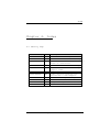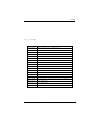
1
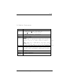
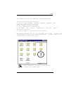
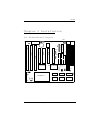
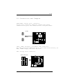
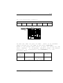
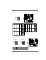
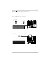
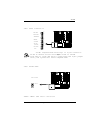
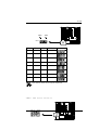
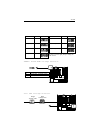
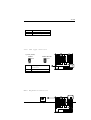
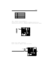
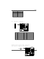
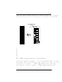
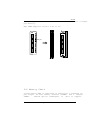
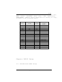
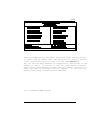
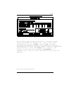
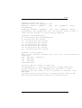
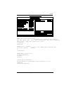
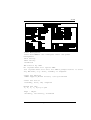
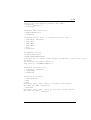
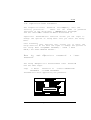
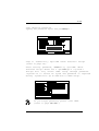
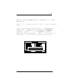
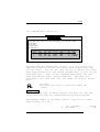
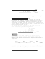
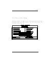
5V-1B 5V-1B MAIN BOARD AT FORM FACTOR USER'S MANUAL ( VER : 1.1 ) Page I 5V-1B Copyright This manual and the information contained herein are protected by copyright. All rights are reserved. Warning and disclaimer This manual is designed to provide information about the Pentium® main board. Every effort has been made to make this manual as accurate as possible, but no warranty or fitness is implied. All the information is provided on an 'as is' basis. The author and his corresponding publishing company shall have neither liability nor responsibility to any person or entity with respect to any loss or damages arising from the information contained in this manual or from the use of the system board that accompanies it. Information contained in this manual is subject to change without notice. The manufacturer of the system board will not be held responsible for technical or editorial omissions made herein, nor for the incidental or consequential damages resulting from its furnishing, performance, functionality or use. Subsequent changes to this manual will be incorporated into the next edition. We welcome any suggestion regarding this manual or our computer products. Trademarks All trademarks are the property of their respective owners. Page II 5V-1B Table Of Contents Chapter 1. Introduction 1 1-1 Overview……………………………………………………..….………….1 1-2 Main Features……………………………………………………………..2 1-3 NoticeHardware of Installation……………………………….………3 1-4 Notice of CD Driver Installation……………………………………...4 Chapter 2. Installation 5 2-1 Motherboard Layout……………….……….… .………..……… ……….5 2-2 Jumper Setting……….. ………..….………………….………….……..6 2-3 Connectors and Jumpers…..……………………………………………7 2-4 SIMM Installation Procedures…………..……….………………..….18 2-5 DIMM Installation Procedures…………………………………..……19 2-6 Memory Chart…………………………………………………………….20 Chapter 3. BIOS Setup 21 3-1 Award® BIOS CMOS Setup…..………………….…….…….………..21 3-2 Standard CMOS Setup………………………….….………….…….…22 3-3 BIOS Features Setup….…………………………………….……..…..24 3-4 Chipset Features Setup …………………………………….…………28 3-5 Power Management Setup……………………………………………..30 3-6 PNP/PCI Configuration Setup…………………………….…………..31 3-7 Integrated Peripherals… ……………………………….………….…..33 3-8 Supervisor/User Password……………………………………...…….35 3-9 IDE HDD Auto Detection………………….…………………………..38 Page III 5V-1B 3-10 Load Setup Defaults…………………………………………….……..41 3-11 Save & Exit Setup…………………………………………….….……..42 3-12 Quit Without Saving………………………………………….…….….43 Chapter 4. Index 44 4-1 Memory Map………………………………………..……..….……..……44 4-2 I/O Map…………………………………………………………………….45 4-3 Time & DMA Channels Map.……………..….…….………………….46 4-4 Interrupt Map……………………………………….……….…………...46 4-5 RTC & CMOS RAM Map………….……………………………….…….47 Page IV 5V-1B Chapter 1 Introduction 1-1 Overview The VT82C580VPX mainboard combines the advanced capabilities of the VIA Apollo VPX chipset with a high performance concurrent PCI local bus architecture to provide the ideal platform for unleashing the unsurpassed speed and processor, Cyrix 6x86 and power of the Intel Pentium AMD K5/K6 processors, and can be easily upgraded for 321 pin ZIF socket. The processor's advanced performance is complemented by a second level write back PB-SRAM up to 1024KB and main memory up to 512MB RAM. The main memory is initialed using the board's two 72-pin SIMM sockets and two 168-pin DIMM sockets that accept either the new high performance EDO, BEDO, Fast Page mode DRAM, or synchronous DRAM(SDRAM). The VT82C580VPX integrates a full set of I/O features on board, including two 16550 UART compatible serial ports, one EPP/ECP capable port, one floppy disk controller, and one infra-red communication controller. On chip built in Enhanced IDE controller provides convenient, high speed PCI bus Master connection capable of four IDE devices, including Hard disk and CD-ROM. Page 1 5V-1B 1-2 Main Features Item Description Socket 7 Supports CPUin a 321- pin ZIF socket A. Intel ® PentiumP54C /P55C MMX CPU B. Cyrix 6x86/6x86L/6x86MX/6x86MII C. AMD K5/K6/K6-2 processors VIA® Apollo VPX chipset 256K; 512K; 1024K 2 DIMM/ 2 SIMM DIMM: A. EDO RAM or Synchronous DRAM with 168-pin DIM modules of 8,16, 32, 64MB, 128MB for 66MHz(5V or 3.3V) Chipset Cache Memory SIMM: take up to 256MB RAM in one bank, using 7 SIMM modules of 1, 2, 4, 8, 16, 32, or 64MB supports for EDO, BEDO or fast page mode memory Exp. Slot 3*16-bit ISA slots and 4* 32-bit PCI expansion slots I/O Integrrted ITE IT8661F/RF multi I/O chipset tha two 16550 UART compatible serial ports, one EP capable port, one floppy disk drive connector, connector Flash ROM 128KB Size 22.0 x 24.0 cm Special AT power connector feature Page 2 5V-1B 1-3 Notice of Hardware Installation A. Check the package before hardware installation The main board package contains: * 5V-1B main board * manual * cables * driver & utility / CD If any of these items is missing or damaged, contact the dealer from whom you purchase. Leave this main board in its original package until you are ready to install it. B. Make Sure power is off during hardware installation C. No guarantee for CPU over-clock setup because system chipset does not support. Page 3 5V-1B 1-4 Notice of CD Driver Installation This CD contains below drivers: A. main boards:I440BX®, I440EX®, I440LX®, I430TX®, VIA® VPX, VP3, and MVP3 main boards B. AGP cards: S- 6326 and T-985 C. Solo-1:Ess-solo-1 sound driver CPU voltage /temperature and fan speed D. GL518SM: detection software E. PCcillin: anti- virus protection software The below drivers are not all suitable for 5V-1B. Please read “ Index” before installing required drivers. “Index” offers all t information on the below files. FILES EDIT VIEW HELP 17 Object(s) Rad “ Index”before installing required drivers. e “Index” file is HTML format. Page 4 5V-1B Chapter 2 Installation 2-1 Motherboard Layout USB BIOS JROM1 JP1 IR KB1 MOUSE P1: AT LPT ISA3 PCI1 PCI2 PCI3 PCI4 ISA2 SIMM2 SIMM1 DIMM2 DIMM1 COM1 COM2 ISA1 VT82C585VPX JCK1 JCK2 JCK3 JCK4 JPW1 JP2 FDC IDE1 IDE2 VT82C586A CACHE CACHE VT82C587AT CACHE CACHE VT82C587AT SOCKET 7 JBF2 JBF1 JBF0 JP3 Page 5 JV1 JD1 JV2 5V-1B 2-2 Jumper Setting Intel® Pentium Processor Installation CPU CLOCK P54C P54C P54C P54C P54C P54C P54C P55C P54C P54C P55C P55C SYS. RATIO JCK CLOCK 1 2 3 4 0 75 MHz 3.3V 50 MHz 1.5X 2-3 2-3 2-3 1-2 OFF 90 MHz 3.3V 60 MHz 1.5X 1-2 2-3 2-3 2-3 OFF 100 MHz 3.3V 66 MHz 1.5X 2-3 1-2 2-3 2-3 OFF 120 MHz 3.3V 60 MHz 2X 1-2 2-3 2-3 2-3 ON 133 MHz 3.3V 66 MHz 2X 2-3 1-2 2-3 2-3 ON 150 MHz 3.3V 60 MHz 2.5X 1-2 2-3 2-3 2-3 ON 166 MHz 3.3V 66 MHz 2.5X 2-3 1-2 2-3 2-3 ON 166 MHz 2.8V/3.3V66 MHz 2.5X 2-3 1-2 2-3 2-3 ON 180 MHz 3.3V 60 MHz 3X 1-2 2-3 2-3 2-3 OFF 200 MHz 3.3V 66 MHz 3X 2-3 1-2 2-3 2-3 OFF 200 MHz 2.8V/3.3V66 MHz 3X 2-3 1-2 2-3 2-3 OFF 233 MHz 2.8V/3.3V66 MHz 3.5X 2-3 1-2 2-3 2-3 OFF JBF 1 OFF OFF OFF OFF OFF ON ON ON ON ON ON OFF 2 OFF OFF OFF OFF OFF OFF OFF OFF OFF OFF OFF OFF JPW1 JV1 JV2 1-2,5-6,7-8 OFF 1-2 1-2,5-6,7-8 OFF 1-2 1-2,5-6,7-8 OFF 1-2 1-2,5-6,7-8 OFF 1-2 1-2,5-6,7-8 OFF 1-2 1-2,5-6,7-8 OFF 1-2 1-2,5-6,7-8 OFF 1-2 7-8 1-2,3-4 1-2 1-2,5-6,7-8 OFF 1-2 1-2,5-6,7-8 OFF 1-2 7-8 1-2,3-4 1-2 7-8 1-2,3-4 1-2 AMD K5/K6/K6-2 Processor Installation CPU CLOCK SYS. CLOCK K5-PR 75 3.52V 50 K5-PR 90/PR120 3.52V 60 K5-PR100/PR133 3.52V 66 K5-PR166 3.52V 66 K6-PR166 2.9V/3.3V 66 K6-PR200 2.9V/3.3V 66 K6-PR233 3.2V/3.3V 66 K6-PR233 3.3V/3.3V 66 K6-PR266 2.2V/3.3V 66 K6-PR300 2.2V/3.45V 66 K6-2 266 2.2V/3.3V 66 (+)K6-2 300 2.2V/3.3V 66 MHz MHz MHz MHz MHz MHz MHz MHz MHz MHz MHz MHz RATIO 1.5X 1.5X 1.5X 2.5X 2.5X 3X 3.5X 3.5X 4X 4.5X 4X 4.5X 1 2-3 1-2 2-3 2-3 2-3 2-3 2-3 2-3 2-3 2-3 2-3 2-3 JCK 2 3 2-3 2-3 2-3 2-3 1-2 2-3 1-2 2-3 1-2 2-3 1-2 2-3 1-2 2-3 1-2 2-3 1-2 2-3 1-2 2-3 1-2 2-3 1-2 2-3 4 1-2 2-3 2-3 2-3 2-3 2-3 2-3 2-3 2-3 2-3 2-3 2-3 0 OFF OFF OFF ON ON OFF OFF OFF ON ON ON ON JBF 1 OFF OFF OFF ON ON ON OFF OFF OFF ON OFF ON 2 OFF OFF OFF OFF OFF OFF OFF OFF ON ON ON ON JPW1 4 1-2 2-3 2-3 2-3 2-3 2-3 2-3 2-3 2-3 2-3 2-3 2-3 0 ON ON ON ON ON ON ON ON ON ON ON OFF JBF 1 OFF OFF OFF OFF OFF OFF OFF OFF OFF OFF ON OFF 2 OFF OFF OFF OFF OFF OFF OFF OFF OFF OFF OFF OFF 1-2,3-4,5-6,7 1-2,3-4,5-6,7 1-2,3-4,5-6,7 1-2,3-4,5-6,7 1-2,7-8 1-2,7-8 5-6,7-8 1-2,5-6,7-8 3-4 3-4 3-4 3-4 JV1 JV2 OFF 1-2 OFF 1-2 OFF 1-2 OFF 1-2 1-2,3-4 1-2 1-2,3-4 1-2 1-2,3-4 1-2 1-2,3-4 1-2 1-2,3-4 1-2 1-2,3-4 2-3 1-2,3-4 1-2 1-2,3-4 1-2 Cyrix 6x86 Processor Installation CPU CLOCK SYS. CLOCK P120+ M1 3.52V 50 MHz P133+ M1 3.52V 55 MHz P150+ M1 3.52V 60 MHz P166+ M1 3.52V 66 MHz P133+ 2.8V/3.3V 55 MHz P150 + 2.8V/3.3V 60 MHz P166+ 2.8V/3.3V 66 MHz P200+ 2.8V/3.3V 75 MHz MX PR 166 2.9V/3.3V 66 MHz MX PR 200 2.9V/3.3V 75 MHz MX PR 233 2.9V/3.3V 75 MHz MII PR 300 2.9V/3.3V 66 MHz RATIO 1 2X 2-3 2X 2-3 2X 1-2 2X 2-3 2X 2-3 2X 1-2 2X 2-3 2X 1-2 2X 2-3 2X 1-2 2.5X 1-2 3.5X 2-3 JCK 2 3 2-3 2-3 2-3 1-2 2-3 2-3 1-2 2-3 2-3 1-2 2-3 2-3 1-2 2-3 2-3 1-2 1-2 2-3 2-3 1-2 2-3 1-2 1-2 2-3 JPW1 1-2,3-4,5-6,7 1-2,3-4,5-6,7 1-2,3-4,5-6,7 1-2,3-4,5-6,7 7-8 7-8 7-8 7-8 1-2,7-8 1-2,7-8 1-2,7-8 1-2,7-8 JV1 JV2 OFF 1-2 OFF 1-2 OFF 1-2 OFF 1-2 1-2,3-4 1-2 1-2,3-4 1-2 1-2,3-4 1-2 1-2,3-4 1-2 1-2,3-4 1-2 1-2,3-4 1-2 1-2,3-4 1-2 1-2,3-4 1-2 Double check the jumper setting and make sure it is correct. (+)Chipset specification does not support100 MHz system clock CPU like AMD® K6-2 300 and K6-2 350, and there is no guarantee for over-clock setup beyond chipse spec. The above K6-2 300 is only for reference and needs to set under 66 Mhz. Page 6 5V-1B 2-3 Connectors and Jumpers COM1/COM2: Serial port connector Serial Port connector supports 16550a high speed communication port that send/receive 16 bytes FIFOs. COM1 COM2 IDE1, IDE2: Primary, Secondary IDE connector PCI IDE controller supports up to four hard disk drivers, CD ROM, 128MB floppy and other devices. FDC: Floopy disk connector IDE2 IDE1 FDC Page 7 5V-1B IR: I.R.(Infra-red) connector Pin1 RX Pin2 GND I.R Connector Pin Out Pin3 Pin 4 Pin5 Pin6 TX +5V RXH VCC Pin7 GND Pin1 IR uses the same I/O port as COM2. There is no hardware the but user jumper setting for I.R./COM2 on this main board needs to set proper BIOS (refer to page 32) setup for “ HP SIR,” “ ASKIR,” or “ Disabled” (default) under “ IR Address Selection” of intergrated Peripherals” according to the following table. BIOS: IRDA 1.0 Integrated Peripherals I.R FunctionUse IRDA 1.0 on I.R.connector Page ASKIR Disabled (default) Use Amplitude Use COM2 shift keyed I.R. on I.R. connect 8 5V-1B JCK1 – JCK3: CPU speed selector Pin 1 JCK1 JCK2 JCK3 JCK4 CPU JCK1 (MHz) 50 2-3 JCK2 JCK3 2-3 55 2-3 60 1-2 Demo. JCK2 JCK3 2-3 CPU JCK1 (MHz) 66 2-3 1-2 2-3 2-3 1-2 75 2-3 1-2 2-3 2-3 1-2 Demo. NOTE: JCK4 is PCI working frequency selector. JCK4: PCI working frequency 32 Mhz: 2-3 CPU/2: 1-2 Pin 1 Pin 1 JCK1 JCK2 JCK3 JCK4 JCK4 1-2 JCK1 JCK2 JCK3 JCK4 PCI working frequency CPU/2 Page 9 5V-1B 2-3 32 MHz (default) JD1: DIMM voltage selector 5V DIMM 3.3V DIMM Pin 1 Pin 1 Pin 7 Pin 7 JD1 DIMM voltage 1-3, 2-4 5V 5-7, 6-8 3.3V (default) JP1: RTC Pin1 JP1 1-2 2-3 RTC Normal (default) Clear CMOS Page 10 5V-1B JP2: Case connector PW-LED + KEYLOCK + SPEAKER + RESET SU-LED SU-SW (SOFTPWR) HD-LED + + + JP3 SU-SW: Suspend Mode Interrupt of 2-pin connector SU-SW is “ Break switch setting.” When SU-SW is turned from open to close and back to open(touch the 2-pin jumper once), the system will enter suspend mode. JP3: Turbo-LED Turbo-LED Pin1 JBF0- JBF2: CPU ratio selector Page 11 5V-1B JBF2 JBF0 Pin1 JBF1 JBF0 off JBF1 off JBF2 off CPU Ratio 1.5x/3.5x on off off 2x on on off 2.5x off on off 3x on off on 4x on on on 4.5x off on on 5.0 x off off on 5.5x Demo. CPU ratio 5x and 5.5x are only for references. JPW1: CPU Vcore seletor Pin 2 Pin 8 Pin 1 Pin 7 Page 12 5V-1B JPW1 3-4 V-core Demo. 2.2V JPW1 5-6,7-8 V-core Demo. 3.2V 1-2,3-4,5- 2.7V 1-2,5-6,7-8 3.3V 7-8 2.8V 1-2,3-4,5-6,7-3.5V 1-2,7-8 2.9V Be sure to set the right jumper setting for CPU Vcore. JROM1: Flash ROM voltage selector Pin1 JROM1 Flash ROM voltage selector 1-2 Winbond®, Atmel®, SST® 2-3 Intel®, MXIC® JV1: CPU voltage selector Single Voltage CPU Pin1 Pin3 Dual Voltage CPU Pin1Page Pin3 13 5V-1B JV1 CPU voltage selector Off Single voltage 1-2,3-4 Dual voltage JV2: CPU type selector Cyrix®, Intel®, AMD® AMD® K6-300 Pin1 Pin1 JV2 1-2 2-3 CPU type(brand) selector Cyrix®, Intel® AMD® AMD® K6-300 KB1: Keyboard Connector Page 14 5V-1B Pin 1 2 3 4 5 Description Keyboard Clock Keyboard Data N.C. Ground +5 Vcc LPT: Parallel Port Connector Parallel Port connector supports standard printer port, enhanced parallel port, extended capabilities parallel (ECP). Mouse: PS/2 mouse connector Mouse connector support 5-pin PS/2 mouse Pin1 Page 15 5V-1B Mouse Pin1 Pin2 Pin3 Pin4 Pin5 P1: PS /2 mouse MS CLK MS Data NC GND VCC AT power connector Pin 1 2 3 4 5 6 Description Power Good +5V DC +12V DC -12V DC GROUND GROUND Pin 7 8 9 10 11 12 Description GROUND GROUND -5V DC +5V DC +5V DC +5V DC USB(Universal Serials Bus) connector USB connector supports USB devices. Pin1 Pin1 Page 16 5V-1B USB1 Pin 1 Pin 2 Pin 3 Pin 4 USB Pint Out USB2 +5V Pin 1 +5V USBP0- Pin 2 USBP1USB P0+Pin 3 USBP1+ GND Pin 4 GND 2-4 SIMM Installation Procedures SIMM memory modules will only fit in one orientation as shown safety tab" because of "plastic a on one end of the SIMM slots which requires the "notched end" of the SIMM memory modules. Page 17 5V-1B Press the memory module firmly into place starting at a 45 degree angle making sure that all the contacts are aligned with the socket. NOTCHED END Pin1 2-5 DIMM Installation Procedures Insert the module as shown. Due to different number of pins on either side of the breaks, the module will only fit in th orientation as shown. DRAM SIMM modules have the same pin contact on both sides. SDRAM DIMM modules have Page 18 5V-1B different pin contacts on each side and therefore have a higher pin density. EDO DIMM supports either 3.3V or 5V. 168 pin 2-6 Memory Chart System memory RAM is comprised of industrial 2 standard 72pin single in-line memory modules (SIMMs) and 2 168-pin DIMMs. TheVIA Apollo VPXchipset is able to support Page 19 5V-1B standard FPM (fast page mode), EDO (extended data out), BEDO (burst extended data out), and synchronous DRAM(SDRAM). Memory can be installed in a variety of cong., as shown in the following table: Total memory Bank 0 (DIMM) 8MB 8MB 12MB 16MB 16MB 24MB 32MB 32MB 32MB 40MB 48MB 64MB 64MB 64MB 72MB 80MB 96MB 128MB 128MB 8MB Bank 1 (DIMM2) Bank2 (SIMM1, SIMM2) 4MB&4MB 8MB 8MB 4MB 8MB 16MB 16MB 32MB 8MB 16MB 32MB 32MB 32MB 8MB 16MB 32MB 8MB&8MB 16MB&16MB 32MB&32MB 64MB 64MB 64MB 64MB 64MB 8MB 16MB 32MB 64MB 64MB&64MB Chapter 3. BIOS Setup 3-1. Award® BIOS CMOS Setup Page 20 5V-1B The menu displays all the major selection items and allow user to select any of shown item. The selection is made by moving cursor (press any direction key ) to the item <Enter> and press key. An on-line help message is displayed at the bottom of the screen as cursor is moving to various items which provides user better understanding of each function. When a selection is made, the menu of selected item will appear. So the user can modify associated configuration parameters. 3-2. Standard CMOS Setup Page 21 5V-1B The ” Standard CMOS Setup” allows user to configure system current dateand time, type of hard disk setting such as drive installed in the system, floppy drive type, and the type of display monitor. Memory size is auto detected by the BIOS and displayed for your reference. When a field is highlighted <Enter> (direction keys to move cursor and key to select). The entries in the field will be changed by<PageDown> pressing or <PageUp> key or user can enter new data directly from the keyboard. Hard Disk Configurations Page 22 5V-1B TYPE : select from "1" to "45" to fill remaining fields with redefined values of disk drives. "USER" Select to fill the "AUTO" to detect the HDD type remaining fields. Select automatically. SIZE :the hard disk size. The unit is mega byte(MB). CYLS : the cylinder number of the hard disk. HEAD :the read/write head number of hard disk. The range is from "1" to "16". PRECOMP the cylinder number at which the disk drive changes the write timing. LANDZ : the cylinder number that the disk drive heads (read/write) are seated when the disk drive is parked. SECTOR : the sector number of each track defined on the hard "1" to"64". disk. The range is from MODE : select "AUTO" to detect the mode type automatically. If LBA mode, select"LBA" or your hard disk supports the "LARGE". However, if your hard disk cyclinder is more than 1024 and does not support the lba function, you have to set at "LARGE.” "NORMAL" if your hard disk supporting Select cylinder is below 1024. If hard disk primary master/slave and secondary master/slave were set“ AUTO,” then the hard disk size and model will be automatically detected on display during post. "Halt on" has options as below: “ No Errors,” “ All, But The system Keyboard,” “ All, But Diskette,” “ All, But Disk/key.” can detect hard disk setup errors during boot-up. For example, means to detect all the setup errors. “Similarly, “ All errors” All, But Keyboard”means all except keyboard error. Default value is “ All Errors.” 3-3. BIOS Features Setup Page 23 5V-1B Menu below shows all of the manufacturer's default values of this main board. Move the cursor by pressing direction keys and <PageDown> or <PageUp> key to modify the parameters, pressing[F1] key to display help message of the selected item. This setup program also provide 2 convenient ways to load the [F6]or CMOS [F7] area if default parameter data from BIOS shown data is corrupted. This provides the system a capability to recover from any possible error. Anti-Virus Protection :Enabled :Disabled (default) CPU Internal Cache Enabled : enable cache Disabled: disable cache External Cache Enabled (default): enable cache Page 24 5V-1B Disabled : disable cache Quick Power On Self Test This category speeds up power on self test. After you power on the computer, if it is set to enable, during post. Enabled : BIOS will shorten or skip some check items. Disabled: normal speed Boot sequence This category determines which drive the system searches first. Take “ A,C,SCSI” for example. System will first search for floppy disk drive; second is hard disk drive, and finally SCSI “ A,C,SCSI.” .Options are as below: drive. Default value is A,C,SCSI; C,A,SCCI, C,CDROM,A; CDROM,C,A; D,A,SCSI; E,A,SCSI; F,A,SCSI; SCSI,A,C; SCSI,C,A; C Only; LS/ZIP,C. Swap Floppy Drive Enabled: floppy A&B will be swapped. Disabled (default): floppy A&B will be not swapped. Boot Up Floppy Seek BIOS will determine if the floppy disk drive is 40 or 80 tracks 360k type is 40 tracks while 720K/ 1.2M and 1.44M are all 80 enabled. tracks. Default value is Boot Up Numlock Status: :On(default) :Off Boot Up System Speed It selects the default system speed which the system will run immediately after power up. High(default): set the speed to high. Low: set the speed to low. Gate A20 Speed :Normal (default) Page 25 5V-1B :Fast Typematic Rate Setting This determines the typematic rate. Enabled: enable typematic rate and typematic delay programming. Disabled: disable typematic rate and typematic delay programming. The system bios will use default value of this 2 items and the default is controlled by keyboard. Typematic Rate(Chars/Sec) 6: 6 Characters Per Second(default) 8: 8 Characters Per Second 10 : 10 Characters Per Second 12: 12 Characters Per Second 15: 15 Characters Per Second 20: 20 Characters Per Second 24: 24 Characters Per Second 30 : 30 Characters Per Second Typematic Delay (Msec) This is the interval between the first and displayed. 250 : 250 msec (default) 500 : 500 msec 750 :750 msec 1000 :1000 msec second character Security Option (refer to page 36) :Setup(default)--- security protection in CMOS setup menu “ Supervisor Password” or User Setting password in BIOS CMOS Password,” the user needs to key in password if entering CMOS setup. BIOS :System---security protection in system boot-up & BIOS setup This function secures both system boot-up and BIOS setup. Page 26 5V-1B Assign IRQ for VGA :Enabled(default) :Disabled Video BIOS Shadow It determines whether video BIOS will be copied to RAM. However, it is optional from chipset design. video shadow will increase the video speed. Enabled : Video Shadow is enabled(default) Disabled: Video Shadow is disabled C8000-CBFFF Shadow, CC000-CFFF Shadow, D0000-D3FFF Shadow: D4000-D7FFF Shadow, D8000-DBFFF Shadow, DC000-DFFF Shadow These are categories determine whether optional ROM will be copied to RAM by 16KB or KB 32 per unit and the size depends on chipset. :Enabled :Disabled (default) 3-4. Chipset Features Setup Page 27 5V-1B DRAM Auto Configuration: the BIOS will automatically detect the CPU speed and will auto-configurate the bus frequency, DRAM speed, cache and read/write cycle. :Disabled :Enabled SDRAM Cycle Length: control the DRAM page missing and row miss leadoff timing. :2 :3 (default) SDRAM Bank Interleave :Disabled(default) :2 bank :4 bank System BIOS Cacheable Define whether system BIOS area cacheable or not. :Enabled :Disabled (default) Page 28 5V-1B Video BIOS Cacheable Define whether video BIOS area cacheable or not. :Enabled :Disabled (Default) Memory Hole At 15MB:this field enable a memory hole in main memory space. CPU cycles matching an enabled hold are passed on to PCI note that a selected can not be changed while the L2 cache is enabled. :Enabled :Disabled(default) USB Keyboard Support: Default value is Disable. If the system uses USB keyboard, “ Enable” for Assign IRQ for please set this item and “also USB” (refer to page 31). 3-5. Power Management Setup Page 29 5V-1B Power Management :User define-users can configure their own power management :Min Saving :Max Saving :Disabled PM Control By APM No :system BIOS will ignore APM. Yes :system BIOS will wait for APM's prompt before it enter any PM mode, e.g. doze, standby or suspend. Video Off Method :DPMS Support, Blank Screen, V/H Sync+Blank Video Off After :Standby, Doze, NA, Suspend Modem Use IRQ 3, 4, 5, 7, 9,10,11,NA IRQ3 – IRQ15 :Primary, Secondary, Disabled Page 30 5V-1B 3-6. PNP / PCI Configuration Setup PNP OS Installed :No(default) OS will not recognize PnP devices. :Yes OS will be responsible to arrange the setup of PnP devices. Resources Controlled By :Manual(default) Reset Configuration Data, The table will show the below “ items: IRQ-3 assigned to, DMA-0 assigned The to.”user can adjust the shown items as required. :Auto The table will not show the above automatically assign the above setup. Page 31 items, and the system will 5V-1B IRQ-3 Assigned To---- IRQ-15 Assigned To : PCI/ISA PnP (default) : Legacy ISA DMA-0 Assigned To--- DMA-7 Assigned To : PCI/ISA PnP (default) : Legancy ISA PCI IRQ Actived By There are 2 modes in activing PCI IRQ. :Edge (default) :Level PCI IDE IRQ Map to: The table will show the below items. :PCI-AUTO (default) , PCI-SLOT1, PCI-SLOT2, PCI-SLOT3, PCI-SLOT4, ISA Choosing either PCI-SLOT1, PCI-SLOT2, PCI-SLOT3, PCI-SLOT4, PCI-AUTO, there are 2 more options. ---Primary IDE INT# (default) : A B,C,D ---Secondary IDE INT# (default) : B B,C,D Assign IRQ for USB : Enable(default) : Disable Assign IRQ for VGA : Enable(default) : Disable Page 32 5V-1B 3-7. Integrated Peripherals IDE Primary Master PIO/ IDE Primary Slave PIO Detect your primary master hard disk device. :Auto (default) :Mode 0,1,2,3,4 IDE HDD Block Mode This feature enhances hard disk performance by making multi sector transfer instead of one sector per transfer. Most of ID drivers, except very early designs ,can use this feature. :Enabled(default) :Disabled IDE Secondary Master PIO/ IDE Secondary Slave PIO This feature detects your secondary master hard disk device. :Auto (default) :Mode 0,1,2,3,4 On-Chip Primary PCI IDE / On-Chip Secondary PCI IDE Page 33 5V-1B Select use chip support primary PCI IDE. : Enabled(default) : Disabled On-Board FDD Controller : Enabled(default) : Disabled On-Board Serial Port 1/ On-Board Serial Port 2 : 3F8/IRQ4 (default) : 2F8/IRQ3 : 3E8/IRQ4 : 2E8/IRQ3 : Auto : Disabled IR Address Select :Disabled(default) :3F8H/2F8H/3E8H/2E8H Choosing any of these items except “disabled”, there are 2 more options: IR mode: HP Sir/Askir/IRDA 1.0 IRQ Select: IRQ10 /3,4,11 (default) On-Board Parallel Port : 378/IRQ7 (default) : 278H/IRQ5 : Disabled Parallel Port Mode : SPP (Default) : EPP : ECP Choosing this item, there is another line shown: ECP Mode Use DMA: 3(default) / 1 : ECP+EPP Choosing this item, there is one more option shown: ECP Mode Use DMA: 3(default) / 1 Page 34 5V-1B 3-8. Supervisor/User Password The "Supervisor/User Password setting" utility sets the security protection. There are two kinds of password Supervisor Password functions in the setup menu : one is “ ,” User Password.”Their difference : is and the other “is Supervisor Password : this function allows you the right to change the options of setup menu once you enter the setup menu. User Password : this function only allows you to enter the setup menu but do not have the right to change the options of “USER PASSWORD,” “ SAVE & EXIT the setup menu except SETUP,” and “ EXIT WITHOUT SAVING.” How to Password” set Supervisor “ Password” & “ User “Supervisor Password”and “ User Password ” The setup of has the same steps. Password in 1: Enter either “ SUPERVISOR PASSWORD” or “ USER PASSWORD” Press<Enter> after appointing the password. Step ENTER PASSWORD: Page 35 5V-1B Step 2:Confirm Password <Enter> . Typing the password again and pressing CONFIRM PASSWORD: “ Security Step 3: Set (refer to page 26). Option” in “ BIOS Features Setup” “ Security Option” After setting password, enter in “ BIOS Features Setup.” There are 2 options “ Setup” & “ System.” “Setup” will only secure CMOS setup through password. “ System” is to secure PC sytem and password is required during system boot- up in addition to CMOS setup.. If you forget password, please clear CMOS (refer to page JP1 10 for RTC ) Page 36 5V-1B How to DisableSupervisor “ Password” & “ User Password” Step 1: Go to CMOS Setup Menu (need to key in password first) Setp 2: Enter “Supervisor Password” or “User Password” After enter, it shows “Enter Password.” <Enter> Press the key "ENTER instead of entering a new password when PASSWORD" “ PASSWORD DISABLED appears. It will inform PRESS ANY KEY TO CONTINUN.” Thus, press any key as instructed. You may disable the password this way. PASSWORD DISABLED!!! PRESS ANY KEY TO CONTINUE… Page 37 5V-1B 3-9. IDE HDD Auto Detection HARD DISK TYPE Primary Master: Primary Slave: Secondary Master: Secondary Slave: SIZE CYLS HEAD PRECOMP LANDZ SECTOR MODE Select Primary Master Option (N: Skip): N OPTIONS SIZE CYLS HEAD PRECOMP LANDZ SECTOR MODE 2 (Y) 4302 523 255 0 8893 63 LBA 1 8894SCO-UNIX) 15 65535 63 installation. NORMAL Note: Some4303 OSes (like must use 8893 “NORMAL” for 3 4296 555 2405 65535 8893 63 LARGE The "IDE HDD AUTO DETECTION" utility is a very useful tool especially when you do not know which kind of hard disk type you are using. You can use this utility to detect the correc disk type installed in the system automatically or you can set hard disk type to auto in the standard CMOS setup. You don't need the"IDE HDD Aauto Detection" utility. The BIOS will auto-detect the hard disk size and model on display during post. HDD modes : The Award® BIOS supports 3 HDD modes: NORMAL, LBA & LARGE. N ormal mode Generic access mode in which neither the BIOS nor the IDE controller will make any transformations during accessing. The maximum number of cylinders, head & mode are1024, 16 & 63. X Page 38 sectors for normal No. Cylinder No. Head (1024) (16) 5V-1B X X No. Sector No. Per Sector (512) 528 MB (63) If user set this HDD to normal mode, the maximum accessible HDD size will be 528 MB even though its physical size may be greater than that! LBA (Logical Block Addressing) Mode A new HDD accessing method to overcome the 528 MB bottleneck. The number of cylinders, heads & sectors shown in setup may not be the number physically contained in the HDD. During HDD accessing, the ide controller will transform the logical address described by sector, head & cylinder into its own physical address inside the HDD. The maximum HDD size supported by LBA mode is 8.4 GB which is obtained by the following formula: No. Cylinder X No. Head X No. Sector No. Bytes Per Sector 8.4 GB X (512) Large Mode Extended HDD access mode supported by Award® software. Some IDE HDDs contain more than 1024 cylinder without LBA support (in some cases, user do not want LBA). The Award® BIOS provides another alternative to support these kinds of large mode: Cyls. Head 1120 560 Sector 16 32 Mode 59 59 NORMAL LARGE BIOS tricks DOS (or other OS) that the number of cylinders is less than 1024 by dividing it by 2. At the same time, the number of heads is multiplied by 2. A reverse transformation Page 39 5V-1B process will be made inside int 12h in order to access the right HDD address the right HDD address! M aximum HDD Size: No. Cylinder X No. Head X No. Sector No. Bytes Per Sector (512) 1 GB X To support LBA or large mode of HDDs, there must be some softwares involved. All these softwares are located in the Award® HDD service routine (int 13h). It may be failed to access a HDD with LBA (large) mode selected if you are running under an perating system which replaces the whole int 13h. Unix operating systems do not support either LBA or large and must utility the standard mode. Unix can support drives larger than 528MB. Page 40 5V-1B 3-10. Load Setup Defaults "Load Setup Defaults" loads optimized settings which are stored in the BIOS ROM. The auto-configured settings only BIOS Features Setup” affect “ and “ Chipset Features Setup” screens. There is no effect on the standard CMOS setup. To use this feature, highlight it on the main screen and press the <Enter> key. A line will appear on screen asking if you want to <Y> key load the setup default values. Press the and then press <N> Press the <Enter> key . The setup defaults will then load. if you don't want to Page 41 5V-1B 3-11 Save & Exit Setup The "Save & Exit Setup" option will bring you back to boot up procedure with all the changes, you have made which are recorded in the CMOS RAM. Page 42 5V-1B 3-12 Quit Without Saving The "Quit Without Saving" option will bring you back to normal boot up procedure without saving any data into CMOS RAM. All of the old data in the CMOS will not be destroyed. Page 43 5V-1B Chapter 4. Index 4-1 Memory Map Address Range 00000-7FFFF 80000-9FBFF 9FC00-9FFFF A0000-C7FFF C8000-DFFFF E0000-EEFFF EF000-EFFFF F0000-F7FFF F8000-FCFFF FD000-FDFFF FE000-FFFFF Size Description 512K Conventional Memory 127K Extended Conventional Memory 1K Extended BIOS Data Area If PS/2 Mouse Is Installed 160K Available For HI Dos Memory 96K Available For HI Dos Memory Adapter ROMS 60K Available For UMB 4K Video Service Routine For Monochrome & CGA Adapter 32K BIOS Cmos Setup Utility 20K BIOS Runtime Service Routine 4K Plug And Play Escd Data Area 8K Bios Runtime Service Routine Page 44 5V-1B 4-2 I/O Map 000-01F 020-021 022-023 040-05F 060-06F 070-07F 080-09F 0A0-0BF 0C0-0DF 0F0-0FF 1F0-1FB 278-27F 2B0-2DF 2F8-2FF 360-36F 378-37F 3B0-3BF 3C0-3CF 3D0-CDF 3F0-3F7 3F8-3FF DMA Controller (Master) Interrupt Controller (Master) Chipset Control Registers. I/O Posts Timer Control Registers Keyboard Interface Controller (8042) Rtc Ports & Cmos I/O Ports DMA Register Interrupt Controller (Slave) Dma Controller (Slave) Math Coprocessor Hard Disk Controller Parallel Port 2 Graphics Adapter Controller Serial Port 2 Network Ports Parallel Port 1 Monochrome & Parallel Port Adapter EGA Adapter CGA Adapter Floppy Disk Controller Serial Port-1 Page 45 5V-1B 4-3 Time & DMA Channels Map Time Map: Timer Channel 0 System Timer Interrupt Timer Channel 1 Dram Refresh Request Timer Channel 2 Speaker Tone Generator DMA DMA DMA DMA DMA DMA DMA DMA DMA Channels: Channel 0 Channel 1 Channel 2 Channel 3 Channel 4 Channel 5 Channel 6 Channel 7 4-4 Nimi: Available Onboard Ecp Floppy Disk Onboard Ecp Cascade For Available Available Available (Option) (Smc Chip) (Default) Dma Controller 1 Interrupt Map Non-Maskable Interrupt IRQ(H/W): 0 System Timer Interrupt From Timer 0 1 Keyboard Output Buffer Full 2 Cascade For IRQ8-15 3 Serial Port2 4 Serial Port1 5 Parallel Port 2 6 Floppy Disk (Smc Chip) 7 Parallel Port 1 8 RTC Clock 9 Available 10 Available 11 Available 12 PS/2 Mouse 13 Math Coprocessor 14 Onboard Hard Disk (IDE1) Channel Page 46 5V-1B 15 Onboard Hard Disk (IDE2) Channel 4-5 RTC & CMOS RAM Map RTC & CMOS:00 Seconds 01 Second Alarm 02 Minutes 03 Minutes Alarm 04 Hours 05 Hours Alarm 06 Day Of Week 07 Day Of Month 08 Month 09 Year 0a Status Register A 0b Status Register B 0c Status Register C 0d Status Register D 0e Diagnostic Status Byte 0f Shutdown Byte 10 Floppy Disk Drive Type Byte 12 Hard Disk Type Byte 13 Reserve 14 Equipment Type 15 Base Memory Low Byte 16 Base Memory High Byte 17 Extension Memory Low Byte 18 Extension Memory High Byte 19-2D 2E-2F Reserved For Extension Memory Low Byte 31 Reserved For Extension Memory High Byte 32 Date Century Byte 33 Information Flag 34-3F Reserve 40-7F Reserved For Chipset Setting Data Page 47 5V-1B ---END Page 48