1
TABLE OF CONTENTS
1.0
2.0
3.0
4.0
OVERVIEW.............................................................................................................................. 2
1.1
CONTROLLER SPECIFICATION............................................................................. 2
1.2
KEY FEATURES...................................................................................................... 3
HARDWARE INTRODUCTION............................................................................................... 5
2.1
BLOCK DIAGRAM....................................................................................................
5
2.2
INTERFACE OVERVIEW.........................................................................................
6
2.3
POWER SUPPLY.....................................................................................................
9
2.4
CLOCK SOURCE.....................................................................................................
10
2.5
MICROCONTROLLER - PIN OUT............................................................................ 10
2.6
LED INTERFACING.................................................................................................. 11
2.7
LCD INTERFACING.................................................................................................. 12
2.8
PULL-UP KEYS INTERFACING................................................................................ 14
2.9
BUZZER INTERFACING........................................................................................... 15
2.10
UNIVERSAL SYNCHRONOUS ASYNCHRONOUS RECIEVER TRANSMITTER. 16
2.11
5V UART.................................................................................................................... 22
2.12
3V3 UART................................................................................................................. 22
2.13
ZIGBEE INTERFACING............................................................................................ 23
2.14
RFID INTERFACING................................................................................................. 24
2.15
ANALOG TO DIGITAL CONVERTER MODULE....................................................... 26
2.16
ICSP CONNECTOR AND RJ-11 PINOUT............................................................... 28
2.17
SERVO MOTOR........................................................................................................ 29
2.18
PORT EXPANDER.................................................................................................... 30
SOFTWARE DEVELOPMENT................................................................................................. 31
3.1
TOOLS AND SOFTWARE......................................................................................... 31
3.2
HOW TO TEST?........................................................................................................ 32
I/O PIN DISTRIBUTION.......................................................................................................... 43
1
1
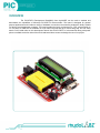
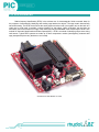
OVERVIEW
The PIC16F877A Development Board(Mini) from rhydoLABZ can be used to evaluate and
demonstrate the capabilities of Microchip PIC16F877A microcontroller. The board is designed for general
purpose applications and includes a variety of hardware to exercise microcontroller peripherals. Ideally suitable
for training and development purposes. The board provides the basic environment for a PIC microcontroller to
run. All ports, 5V,GND,3V3 are available on 40 pin male berg strip and 44 pin female berg strip. We can easily
attach a mini bread board on this development board. Now all the PORTs of microcontroller along with power
pins are available at the four side of the mini bread board where as we can design the rest of our project.
2
1.1. CONTROLLER SPECIFICATION
PIC microcontrollers are manufactured by Microchip Technology Inc. The PIC microcontroller family
is based on modified Harvard architecture. Features of PIC16F877A microcontrollers are
1. Only 35 single-word instructions to learn
2. All single-cycle instructions except for program branches, which are two-cycle
3. Operating speed:
- DC – 20 MHz clock input
- DC – 200 ns instruction cycle
4. Up to 8K x 14 words of Flash Program Memory
5. Up to 368 x 8 bytes of Data Memory (RAM)
6. Up to 256 x 8 bytes of EEPROM Data Memory
7. Pinout compatible to other 28-pin or 40/44-pin PIC16CXXX and PIC16FXXX microcontrollers
8. Timer0: 8-bit timer/counter with 8-bit prescaler
9. Timer1: 16-bit timer/counter with prescaler, can be incremented during Sleep via external crystal/clock
10. Timer2: 8-bit timer/counter with 8-bit period register, prescaler and postscaler .
11. Two Capture, Compare, PWM modules
- Capture is 16-bit, max. resolution is 12.5 ns
- Compare is 16-bit, max. resolution is 200 ns
- PWM max. resolution is 10-bit
12. Synchronous Serial Port (SSP) with SPI™ (Master mode) and I2C™(Master/Slave)
13. Universal Synchronous Asynchronous Receiver Transmitter (USART/SCI) with 9-bit address detection
14. Parallel Slave Port (PSP) – 8 bits wide withexternal RD, WR and CS controls (40/44-pin only)
15. Brown-out detection circuitry for Brown-out Reset (BOR)
16. 10-bit, up to 8-channel Analog-to-Digital Converter (A/D)
17. Brown-out Reset (BOR)
18. Analog Comparator module with:
- Two analog comparators
- Programmable on-chip voltage reference (VREF) module
- Programmable input multiplexing from device inputs and internal voltage reference
- Comparator outputs are externally accessible
19. 100,000 erase/write cycle Enhanced Flash program memory typical
20. 1,000,000 erase/write cycle Data EEPROM memory typical
21. Data EEPROM Retention > 40 years
22. Self-re programmable under software control
23. In-Circuit Serial Programming™ (ICSP™) via two pins
24. Single-supply 5V In-Circuit Serial Programming
25. Watchdog Timer (WDT) with its own on-chip RC oscillator for reliable operation
26. Programmable code protection
27. Power saving Sleep mode
28. Selectable oscillator options
29. In-Circuit Debug (ICD) via two pin
30. Low-power, high-speed Flash/EEPROM technology
31. Fully static design
32. Wide operating voltage range (2.0V to 5.5V)
33. Commercial and Industrial temperature ranges
34. Low-power consumption
3
1
1.2. KEY FEATURES OF PIC16F877A DEVELOPMENT BOARD-MINI
1.
2.
3.
4.
5.
6.
7.
8.
9.
10.
11.
12.
13.
14.
15.
16.
17.
18.
19.
20.
21.
22.
23.
24.
25.
Compact and Ready to use
Professional EMI/RFI Complaint PCB Layout for Noise Reduction
High Quality Two layer PTH PCB
The board is moderate in size
Board supports 40 pin PIC microcontrollers
No separate power adapter required(USB power source)
RMC Connector and barrel jack connector for external power supply (with jumper select option)
RS232 and CP2102 Interface (for direct connection to PC's serial/USB port)
On board two line LCD display(2x16)
On board Reset button
Built in potentiometer interface for ADC
On board Temperature Sensor Interface
On board Buzzer Interface
On board JTAG connector for Debugging/Programming
On board ICSP connector for Debugging/Programming
On board 20 MHz crystal oscillator
On board DB9 female connector
On board mini USB connector
On board 5V UART pins.
On board 3V3 UART pins.
There is a provision to interface ZigBee module
There is a provision to interface RFID module
There is a provision to interface servomotor
There is a provision to attach mini bread board
Male and Female berg strips to access port pins
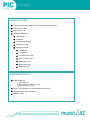
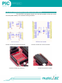
LAYOUT OF PIC16F877A DEVELOPMENT BOARD-MINI
4
PACKAGE CONTENTS
•
•
•
•
Fully Assembled and Tested PIC16F877A Development board-mini
RS232 Serial Cable
USB cable A to B
Software CDROM with
•
•
•
•
•
User Manual
Schematic
Programming Software
Sample Hex Code
Example Codes for
•
•
•
•
•
•
•
Led Blinking
LCD Display
Led Control with Timer
UART Communication
PWM Generation
Buzzer Interfacing
ADC Interfacing
SYSTEM SPECIFICATION
•
•
•
•
Power Supply via
1. USB cable(5V)
2. DC barrel jack connector(7-12V)
3. RMC connector(7-12V)
50mA in idle state(when On-board modules are inactive)
Dimension is 82.34mm x 96.08mm
Weight is ~92g
5
1
HARDWARE INTRODUCTION
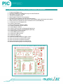
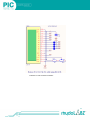
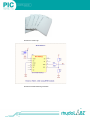
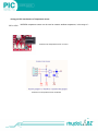
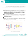
2.1. BLOCK DIAGRAM
6
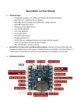
2.2. INTERFACE OVERVIEW
Illustration 1:Top view of the Development board -Mini
Illustration 2:Bottom view of the Development board -Mini
7
1
PERIPHERALS
DESCRIPTIONS
U1
POWER SUPPLY- LD1117 3V3
U2
RS232 - MAX232
U3
VOLTAGE REGULATOR- LM7805
U4
CONTROLLER - PIC16F877A
U5
USB Interface-CP2102
U6
MCP2551(used only in PIC18F4580 dev board)
U7
TEMPERATURE SENSOR -MCP9700
U8
Connector for ZIGBEE MODULE
P1
LCD Contrast Control Knob
P2
ADC Knob
SW4
Reset switch
SW1,SW2,SW3
Pull up key
LED1,LED2,LED3
3 LEDs connected to the PORTB pins
LCD
16X2 Monochrome LCD
K11
RJ-11 Connector (ICSP)
K3
USB Socket
K9
RMC connector
K5
DB9 Female Connector
K10
ICSP Connector
K1,K2,K7,K8,K12,K13
Controller Port pins
K14
CAN Interface (used only in PIC18F4580 dev board)
K15 & K17
5V UART & 3V3 UART
K16
Connector for servomotor
8
JUMPER
No.
DESCRIPTIONS
SET OPTIONS
SETTINGS
DESCRIPTION
Power Supply
Options
1-2
Select USB power
J18
2-3
Select external DC power
J11, J12, J13, J14
LCD
Short access
Enables LCD for 8-bit mode
J16
Potentiometer
Short access
Enables ADC connection via
POT
J17
Temperature Sensor
Short access
Enables temp sensor
connection
J1, J2, J10
LED
Short access
Enables LED connection
J8,J9,J15
Pull-Up Key
Short access
Enables Pull-Up Key connection
J19
Buzzer
Short access
Enables buzzer connection
J20,J21
ZigBee
Short access
Establish ZigBee connection
1-2
RS232 Connection
J3, J4
USART
2-3
USB Connection
9
1
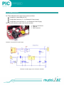
2.3. POWER SUPPLY
PIC16F877A Board has three power supply options as follows:
•
•
•
Through the on board USB port (5V)
Through RMC Connector (7V - 12V External DC Power Supply)
Through Barrel Jack Connector (7V - 12V External DC Power Supply)
Note: For power selection, jumper (J18) must be in position.
1. Barrel Jack Connector
2. USB port
3. RMC Connector
Illustration 3: Connectors for power supply
Illustration 4: Power supply source connection schematic
10
2.4. CLOCK SOURCE
PIC microcontrollers normally use a quartz crystal for the purpose
of providing clock frequency. Clock source for PIC16F877A Development
board -Mini:
•
20 MHz Crystal as the MCU clock source
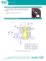
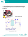
2.5. MICROCONTROLLER PINOUT
Illustration 4: Microcontroller pinout schematic
11
1
2.6. LED INTERFACE
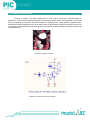
LED’s are semiconductor diodes, electronic devices that permit current to flow in only one direction. The
diode is formed by bringing two slightly different materials together to form a PN junction. In a PN junction, the P
side contains excess positive charge ("holes") while the N side contains excess negative charge (“electrons”).
When a forward voltage is applied to the semiconducting element forming the PN junction, electrons move from
N area toward P area and holes move from P area toward N area. Near the junction, the electrons and holes
combine. As this occurs, energy is released in the form of light that is emitted by the LED. The material used in
the semi conducting element of an LED determines its color. LED’s are the simplest devices to test port
functioning.
There are 3 LED available in our development board. General Purpose Input Output RB1,RB2 and RB3
are interfaced with LEDs via jumpers J1,J2 and J10 respectively.
Illustration 5: LEDs on board
Illustration 6:LED connection schematic
12
2.7. LCD INTERFACE
The display is a standard 16x2 LCD which displays 2 lines of 16 characters. Each character is 40 pixels,
making it 1280 pixels overall. The display receives ASCII codes for each character at the data inputs(D0-D7).
The data is presented to the display inputs by MCU, and latched in by triggering the E(Enable) input. The
RW(Read/Write) line can be tied low(write mode),as the LCD is receiving data only. The RS(Register Select)
inputs allows commands to be send to the display. RS select command/data register. The display itself contains
a microcontroller, the standard chip in this type of display is Hitachi HD44780U. It must be initialized according to
the data and display options required.
The module can be used in 4-bit or 8-bit mode. In our development board, we could use either 4bit or 8-bit interfaces. Shorting jumpers J11, J12, J13, J14 selects 8-bit interface & if removed selects 4-bit
interface. PORTD pins are used as data/command pins while PORTC pins as RS & E pin. A trimmer
potentiometer is interfaced to adjust the LCD contrast to get a better view in every angle.
Note: Jumpers J11, J12, J13 & J14 will be shorted in PCB by default. If RD0, RD1, RD2 & RD3 needs to
relieved from LCD connection, user needs to manually disconnect the track lying underneath these jumpers.
Trimmer Pot
Illustration 7:LCD's male port on board
Illustration 8:16x2 alphanumeric LCD placed on board
13
1
Illustration 9: LCD connection schematic
14
2.8. PULL-UP KEY INTERFACING
The simplest input to a microcontroller is a switch or push button. This can operate with just one
additional support component, a pull-up resistor. The resistors R15, R14 and R34 are pull up resistors. The input
pins RC3, RC2 and RB5 reads high value when the keys are not pressed. When the key is pressed, it connect
the input pin to the ground via a small value resistor. Thus input pin get logic low value. There are 3 pull up
switches in the board connected to RC2, RC3 and RB5.
Illustration 10:Pull Up Key on board
Illustration 11: Pull up key connection schematic
15
1
2.9. BUZZER INTERFACING
A buzzer or beeper is an audio signaling device, which may be mechanical, electromechanical or
piezoelectric. Typical uses of buzzers and beepers include alarm devices, timers and confirmation of user input
such as a mouse click or keystroke. A buzzer or beeper is a signaling device, usually electronic, typically used in
automobiles household appliances such as microwave oven or game shows. It indicates a warning in the form of
a continuous or intermittent buzzing or beeping sound. Here we use a ceramic-based piezoelectric sounder with
a high-pitched tone.
Illustration 12: Buzzer on board
Illustration 13: Buzzer Connection Schematic
16
2.10. UNIVERSAL SYNCHRONOUS AND ASYNCHRONOUS RECEIVER AND
TRANSMITER
Serial communication is the process of sending data one bit at a time sequentially over a
communication channel. The Universal Synchronous Asynchronous Receiver Transmitter(USART) module is
one of the two serial I/O modules. USART is also known as a Serial Communication Interface. The USART is
highly flexible serial communication protocol.
The USART can be configured as a full duplex asynchronous system that can communicate with
peripheral devices such as CRT terminals and personal computers, or it can be configured as a half duplex
synchronous system that can communicate with peripheral devices such as A/D or D/A integrated circuits, serial
EEPROMs etc.
Note- The baud rate range for the PIC microcontroller is 300 to 115200.
The main features are:
•
•
•
•
•
•
•
•
•
•
Full duplex operations
Asynchronous or synchronous operation
Master or slave clocked synchronous operation
High resolution Baud Rate generator
Odd or even parity check supported by hardware
Data Over-Run detection
Framing Error Detection
Noise filtering includes false start bit detection and digital low pass filter
Multiprocessor communication mode
Double speed asynchronous communication mode
17
1
RS-232 Interfacing
RS-232 is a standard communication protocol for linking computer and its peripheral devices to allow
serial data exchange. Since RS-232 communication voltage levels are different than microcontroller logic levels,
it is necessary to use a RS-232 Transceiver circuit. Here we use serial driver IC MAX232 for interfacing RS-232
with microcontroller UART module. A DB9 female connector is provided to make direct connection with the serial
port of a device or PC.
Illustration 14: RS232 Module on board
Illustration 15:RS232 Module Schematic
18
CP2102 USB Interfacing
The CP2102 is a highly-integrated USB to UART Bridge Controller providing a simple solution for
updating RS-232 designs to USB using a minimum of components and PCB space. The CP2102 includes a USB
2.0 full-speed function controller, USB transceiver, oscillator, EEPROM and asynchronous serial data bus
(UART) with full modem control signals in a compact 5 x 5 mm MLP-28 package. No other external USB
components are required.
Illustration 12: CP2102 Module
Illustration 13: CP2102 Module schematic
19
1
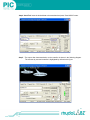
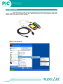
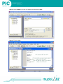
USING REALTERM IN PC
Real term is a testing, analyzing and simulation tool for serial communication protocols. It allows us to
monitor communication between two serial devices or to test the serial communication of a single devices.
Realterm can be download by (download)
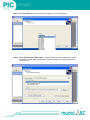
Steps for creating RealTerm in PC
The serial data transmitted through USART can be viewed on a PC using a Windows tool for Serial Port
Communication called Realterm.
Step 1: All program
RealTerm
realterm
20
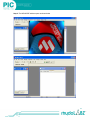
Step 2: Display Tab- Here the output text format selected is ANSI and Half Duplex mode is
enabled to view the data sent by the user.
Step 3: Port Tab-To test the connection - make sure the Open button is
pressed, Select required baud rate and the “Port” dropdown here, select the number of
your COM port and then press the Change button.
21
1
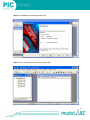
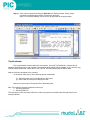
Step 4: Send Tab- Insert the desired data to be transmitted and press "Send ASCII" button.
Step 5 : The output after data transmission to the controller is shown in the following diagram.
The text sent by user and controller is highlighted by callouts in the figure.
22
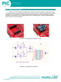
2.11. 5V UART
5V UART can be used to interface 5V TTL modules to communicate with microcontroller.
Eg:- RFID, Bluetooth etc
Remove J3&J4, while using K15 as UART
Illustration 14: 5V UART Schematic
Illustration 15: 5V UART pins
2.12. 3V3 UART
3V3 UART can be used to interface 3V3 TTL modules to communicate with microcontroller.
Eg:- ZigBee, BlueBee etc
Illustration 16: 3V3 UART Schematic
Illustration 17: 3V3 UART pins
23
1
2.13. ZIGBEE INTERFACING
ZigBee is a wireless networking standard that is aimed at remote control and sensor applications which
is suitable for operation in harsh radio environments and in isolated locations. ZigBee technology builds on IEEE
standard 802.15.4. rhydoLABZ PIC16F877A development board(mini) have pin-out compatibility for ZigBee
interfacing. Communication with the ZigBee module uses a standard UART interface compatible with 3V3.
Short J20 and J21 while using ZigBee.
Illustration 22: ZigBee Module mounted on board
Illustration 23: ZigBee Module Schematic
24
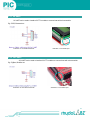
2.14. RFID INTERFACING
Radio-frequency identification (RFID) is the wireless use of electromagnetic fields to transfer data, for
the purposes of automatically identifying and tracking tags attached to objects. The tags contain electronically
stored information. The RFID device serves the same purpose as a bar code or a magnetic strip on the back of a
credit card or ATM card; it provides a unique identifier for that object. Unlike a barcode, the tag does not
necessarily need to be within line of sight of the reader and may be embedded in the tracked object. RFID is one
method for Automatic Identification and Data Capture(AIDC) . RFID is a method of identifying unique items using
radio waves. Typical RFID systems are made up of three components: readers (interrogators), antennas and
tags (transponders) that carry the data on a microchip.
Illustration 30: RFID Reader on board
25
1
Illustration 31:RFID Tags
Illustration 32:RFID Interfacing Schematic
26
2.15. ANALOG-TO-DIGITAL CONVERTER
The Analog-to-Digital Converter module in PIC16F877A has eight analog inputs . The analog
input charges a sample and hold capacitor . The output of the sample and hold capacitor is the input into the
converter. The converter then generates a digital result of this analog level via successive approximation . The
A/D conversion of the analog input signal results in a corresponding 10-bit digital number. The A/D module has
four registers. These registers are:
• A/D Result High Register(ADRESH)
• A/D Result Low Register(ADRESL)
• A/D Control Register0(ADCON0)
• A/D Control Register1(ADCON1)
Analog pin RA0 connected to a potentiometer
A potentiometer in an electrical device allows reducing the voltage level from the circuit
maximum to ground, or zero level. The test input voltage for ADC is derived from a 10K potentiometer connected
across the +5V power supply, and is connected to RA0/AN0 pin of PIC16F877A. Therefore, the 10-bit ADC will
convert any analog voltage between 0-5V to a digital number ranging from 0-1023. The number will be displayed
on the LCD. The device that performs either conversion is called an A/D or analog-to-digital converter.
Illustration 18: Potentiometer for ADC
Illustration 19: Potentiometer for ADC Schematic
27
1
Analog pin RA1 interfaced to a Temperature sensor
MCP9700 temperature sensor can be used to measure ambient temperature, in the range of 55C to 150C.
Illustration 20:Temperature Sensor on board
Illustration 21:Temperature Sensor Schematic
28
2.16. ICSP CONNECTOR AND RJ-11 PINOUT
In-Circuit Serial Programming, is the ability of some programmable devices, microcontrollers and
other embedded devices to be programmed while installed in a complete system. This is a Six PIN male
connector used to upload/debug programs to microcontroller. Pinout of RJ-11 is same as that of ICSP , so it can
be used for debugging/programming the controller.
Signals and pinout
•
•
•
•
•
Vpp - Programming mode voltage. This must be connected to the MCLR pin, or the Vpp pin of the
optional ICSP port available on some large-pin count PICs. To put the PIC into programming mode, this
line must be in a specified range that varies from PIC to PIC. For 5V PICs, this is always some amount
above Vdd, and can be as high as 13.5V. The 3.3V only PICs like the 18F, 24H, and 33F series use a
special signature to enter programming mode and Vpp is a digital signal that is either at ground or Vdd.
There is no one Vpp voltage that is within the valid Vpp range of all PICs. In fact, the minimum required
Vpp level for some PICs can damage other PICs.
Vdd - This is the positive power input to the PIC. Some programmers require this to be provided by the
circuit (circuit must be at least partially powered up), some programmers expect to drive this line
themselves and require the circuit to be off, while others can be configured either way (like the Microchip
ICD2). The Embed Inc programmers expect to drive the Vdd line themselves and require the target
circuit to be off during programming.
Vss - Negative power input to the PIC and the zero volts reference for the remaining signals. Voltages of
the other signals are implicitly with respect to Vss.
ICSPCLK - Clock line of the serial data interface. This line swings from GND to Vdd and is always driven
by the programmer. Data is transferred on the falling edge.
ICSPDAT - Serial data line. The serial interface is bi-directional, so this line can be driven by either the
programmer or the PIC depending on the current operation. In either case this line swings from GND to
Vdd. A bit is transferred on the falling edge of PGC.
Illustration 24:ICSP Port and RJ-11 Port Schematic
29
1
Illustration 24:ICSP Port on Development Board-mini
Illustration 25:Rj-11 Pinout
2.17. SERVO MOTOR INTERFACING
A servomotor is a rotary actuator that allows for precise control of angular position, velocity and
acceleration. It consists of a suitable motor coupled to a sensor for position feedback. Servomotors are
controlled by sending an electrical pulse of variable width, or pulse width modulation (PWM), through the control
wire. There is a minimum pulse, a maximum pulse and a repetition rate. Here the control line is connected to the
RE1 pin of the microcontroller. The control signal can be created by using by timers with required duty cycle .
Illustration 26:Servo motor
Illustration 27:Servo motor connector Schematic
30
2.18. PORT EXPANDER(ADDITIONAL INPUT/OUTPUT PORTS)
The PIC16F877A development board- has all port pins available at direct port access
connectors(male & female). The connections are as given below.
Illustration 33:GPIO near breadboard Schematic
Illustration 35:GPIO near breadboard
Illustration 34:GPIO near controller Schematic
Illustration 36:GPIO near controller
31
1
SOFTWARE DEVELOPMENT
3.1. TOOLS AND SOFTWARE
To get started with PIC microcontrollers we will need some tools and software:
•
•
•
•
•
A PC, desktop or laptop with a spare USB port, running Windows 7 or XP.
Microchips MPLAB Integrated Development Environment.
A C compiler
A PIC programmer, to load your programs onto the microcontroller without bootloader.
A prototyping environment, such as rhydoLABZ PIC16F877A Microcontroller Development Boards.
The MPLAB development system consists of a system of programs that run on a PC. This software package is
designed to help develop, edit, test, and debug PIC code. Installing the MPLAB package is straightforward and
simple.
Familiarization of MPLAB LITE Development Suite
•
Creating a Project file
•
Select Microcontroller from Device Database
•
Copy and Add the CPU Startup Code
•
Create New Source Files
•
Add Source Files to Project
•
Set Tool Options for Target
32
3.2. HOW TO TEST?
Mini USB and Serial Cable are used for programming the Development board -Mini. When USB
cable is connected to the Development board -Mini, “PWR LED”(Red) on the top of Development board -Mini
module glows, which shows the power indication.
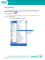
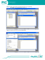
Step 1 :Launch MPLAB IDE
33
1
Step 2 :The MPLAB IDE window opens as shown below
34
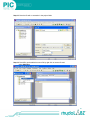
Step 3 :To create a new project, select Project > Project Wizard from menu bar
Step 4 :Click 'Next' to the poped up Project Wizard window
35
1
Step 5: Select PIC16F877A from the drop-down list appears in the window opens
Step 6: Select HI-TECH PICC TOOL suite as compiler among the list of toolsuite given. Check
the toolsuite content listed contains PICC Compiler suiting to our programming needs.
And click next.
36
Step 7: Create a project file at desired name in a suitable location with appropriate name
Step 8: In next window open, add any files you desire to add to your new project,if required. else
just skip this step by clicking 'Next'.
37
1
Step 9: Click Finish to the following window open.
Step 10: After creating project the following window open.
38
Step 11: Create a new file either by clicking the New File icon, or by selecting
File > New or using keyboard shortcut CTRL + N.
Step 12: Created file was saved by selecting File>Save as
39
1
Step 13: Save the file with .c extension in the project folder
Step 14: Saved file can be added to source file by right click on source file and
select Add Files.
40
Step 15: Select sample.c from the new window opened and click Open.
Step 16: Type the code.
41
1
Step 17: Code can be compile by clicking the Build All icon. Build the project. Errors (if any)
get listed in the Build output window. Correct them and build
again. On successful building, the hex file will be generated in the project folder.
Tiny Bootloader
This is a bootloader for Microchip PIC microcontroller . By using Tiny Bootloader , program can be
upload to the flash memory of the controller. The communication settings can be editable, so we can write any
COM and desired baud rate. Works with PIC16F,PIC18F and automatically detects HEX content.
Now the code can be flashed to the controller.
In the board, make sure to do the following jumper connections
(1) Select the power source as USB cable or DC source.
(2) Select USB or serial port for flashing the code.
Now power up the board. The power LED on the board glows.
Note: The controller can be programmed in two ways
1. By using Serial Port
2. By using USB Port
The user has to choose the exact COM Port in order to program the controller either through Serial Port or
through USB Port.
42
Step 18: Open Tiny Bootloader . Load required hex file.
Step 19: Click Write Flash and simultaneously press Reset button on development on development
board. After successfully flashing the code into the controller, it can be used for the
desired purpose.
43
1
I/O DISTRIBUTION
4.1. THE PIN DISTRIBUTION OF PIC16F877A DEVELOPMENT BOARD
Pin No:
Name
Type
The I/O assign of PIC16F877A
Development Board
1
MCLR/VPP
-
Reset Key
2
RA0/AN0
I/O
ADC Input (potentiometer)
3
RA1/AN1
I/O
ADC Input (Temp Sensor)
4
RA2/AN2/VREF-
I/O
N/C
5
RA3/AN3/VREF+
I/O
N/C
6
RA4/T0CKI
-
N/C
7
RA5/AN4/SS
I/O
N/C
8
RE0/RD/AN5
I/O
BUZZER
9
RE1/WR/AN6
I/O
SERVOMOTOR
10
RE2/CS/AN7
I/O
N/C
11
VDD
-
5V (Vcc)
12
VSS
-
GND
13
OSC1/CLKIN
-
-
14
OSC2/CLKOUT
-
-
15
RC0/T1OSO/T1CKI
I/O
LCD
16
RC1/T1OSI/CCP2
I/O
LCD
17
RC2/CCP1
I/O
Pull-Up Key
18
RC3/SCK/SCL
I/O
Pull-Up Key
19
RD0/PSP0
I/O
LCD
20
RD1/PSP1
I/O
LCD
21
RD2/PSP2
I/O
LCD
22
RD3/PSP3
I/O
LCD
23
RC4/SDI/SDA
I/O
N/C
24
RC5/SDO
I/O
N/C
25
RC6/TX/CK
I/O
TXD/ XBEE/RFID
26
RC7/RX/DT
I/O
RXD /XBEE/RFID
27
RD4/PSP4
I/O
LCD
44
28
RD5/PSP5
I/O
LCD
29
RD6/PSP6
I/O
LCD
30
RD7/PSP7
I/O
LCD
31
VSS
-
GND
32
VDD
-
5V (Vcc)
33
RB0/INT
I/O
N/C
34
RB1
I/O
LED
35
RB2
I/O
LED
36
RB3/PGM
I/O
LED
37
RB4
I/O
N/C
38
RB5
I/O
Pull-Up Key
39
RB6/PGC
I/O
ICSP
40
RB7/PGD
I/O
ICSP
45
1
TECHNICAL SUPPORT
If you are experiencing a problem that is not described in this manual, please contact us.
Our phone lines are open from 9:00 AM – 5.00 PM (Indian Standard Time) Monday
through Saturday excluding holidays. Email can be sent to [email protected]
DISCLAIMER
Copyright © Rhydo Technologies (P) Ltd.
All rights are reserved. Reproduction in whole or in part is prohibited without the prior written consent of the
copyright owner. The information presented in this document does not form part of any quotation or
contract, is believed to be accurate and reliable and may be changed without notice.
Contact Us
Rhydo Technologies (P) Ltd.
(An ISO 9001:2008 Certified R&D Company)
Golden Plaza, Chittoor Road, Cochin – 682018, Kerala, India.
Tel: 0091 484 2370 444, 2371 666, Cell: 0091- 99466 70444
Fax: 0091 484 237 0579, Email: [email protected], [email protected]
For more information please visit: www.rhydolabz.com