1
Preliminary User’s Manual
ERTEC 400
Enhanced Real-Time Ethernet Controller
32-Bit RISC CPU Core
Hardware
µPD800232F1-012-HN2
Document No. A17812EE1V1UM00
Date Published July 2007
© NEC Electronics Corporation 2007
Printed in Germany
NOTES FOR CMOS DEVICES
1
VOLTAGE APPLICATION WAVEFORM AT INPUT PIN
Waveform distortion due to input noise or a reflected wave may cause malfunction. If the input of the
CMOS device stays in the area between VIL (MAX) and VIH (MIN) due to noise, etc., the device may
malfunction. Take care to prevent chattering noise from entering the device when the input level is fixed,
and also in the transition period when the input level passes through the area between VIL (MAX) and
VIH (MIN).
2
HANDLING OF UNUSED INPUT PINS
Unconnected CMOS device inputs can be cause of malfunction. If an input pin is unconnected, it is
possible that an internal input level may be generated due to noise, etc., causing malfunction. CMOS
devices behave differently than Bipolar or NMOS devices. Input levels of CMOS devices must be fixed
high or low by using pull-up or pull-down circuitry. Each unused pin should be connected to VDD or GND
via a resistor if there is a possibility that it will be an output pin. All handling related to unused pins must
be judged separately for each device and according to related specifications governing the device.
3
PRECAUTION AGAINST ESD
A strong electric field, when exposed to a MOS device, can cause destruction of the gate oxide and
ultimately degrade the device operation. Steps must be taken to stop generation of static electricity as
much as possible, and quickly dissipate it when it has occurred. Environmental control must be
adequate. When it is dry, a humidifier should be used. It is recommended to avoid using insulators that
easily build up static electricity. Semiconductor devices must be stored and transported in an anti-static
container, static shielding bag or conductive material. All test and measurement tools including work
benches and floors should be grounded. The operator should be grounded using a wrist strap.
Semiconductor devices must not be touched with bare hands. Similar precautions need to be taken for
PW boards with mounted semiconductor devices.
4
STATUS BEFORE INITIALIZATION
Power-on does not necessarily define the initial status of a MOS device. Immediately after the power
source is turned ON, devices with reset functions have not yet been initialized. Hence, power-on does
not guarantee output pin levels, I/O settings or contents of registers. A device is not initialized until the
reset signal is received. A reset operation must be executed immediately after power-on for devices
with reset functions.
5
INPUT OF SIGNAL DURING POWER OFF STATE
Do not input signals or an I/O pull-up power supply while the device is not powered. The current
injection that results from input of such a signal or I/O pull-up power supply may cause malfunction and
the abnormal current that passes in the device at this time may cause degradation of internal elements.
Input of signals during the power off state must be judged separately for each device and according to
related specifications governing the device.
All other product, brand, or trade names used in this publication are the trademarks
or registered trademarks of their respective trademark owners.
Product specifications are subject to change without notice. To ensure that you have the latest
product data, please contact your local NEC Electronics sales office.
2
Preliminary User’s Manual A17812EE1V1UM00
• The information contained in this document is being issued in advance of the production cycle for the
product. The parameters for the product may change before final production or NEC Electronics
Corporation, at its own discretion, may withdraw the product prior to its production.
• Not all products and/or types are available in every country. Please check with an NEC Electronics sales
representative for availability and additional information.
• No part of this document may be copied or reproduced in any form or by any means without the prior written consent
of NEC Electronics. NEC Electronics assumes no responsibility for any errors that may appear in this document.
• NEC Electronics does not assume any liability for infringement of patents, copyrights or other intellectual property
rights of third parties by or arising from the use of NEC Electronics products listed in this document or any other
liability arising from the use of such products. No license, express, implied or otherwise, is granted under any
patents, copyrights or other intellectual property rights of NEC Electronics or others.
• Descriptions of circuits, software and other related information in this document are provided for illustrative purposes
in semiconductor product operation and application examples. The incorporation of these circuits, software and
information in the design of a customer's equipment shall be done under the full responsibility of the customer. NEC
Electronics assumes no responsibility for any losses incurred by customers or third parties arising from the use of
these circuits, software and information.
• While NEC Electronics endeavors to enhance the quality, reliability and safety of NEC Electronics products,
customers agree and acknowledge that the possibility of defects thereof cannot be eliminated entirely. To minimize
risks of damage to property or injury (including death) to persons arising from defects in NEC Electronics products,
customers must incorporate sufficient safety measures in their design, such as redundancy, fire-containment and
anti-failure features.
• NEC Electronics products are classified into the following three quality grades: "Standard", "Special" and "Specific".
The "Specific" quality grade applies only to NEC Electronics products developed based on a customer-designated
"quality assurance program" for a specific application. The recommended applications of an NEC Electronics
products depend on its quality grade, as indicated below. Customers must check the quality grade of each NEC
Electronics product before using it in a particular application.
"Standard": Computers, office equipment, communications equipment, test and measurement equipment, audio and
visual equipment, home electronic appliances, machine tools, personal electronic equipment and
industrial robots.
"Special": Transportation equipment (automobiles, trains, ships, etc.), traffic control systems, anti-disaster
systems, anti-crime systems, safety equipment and medical equipment (not specifically designed for life
support).
"Specific": Aircraft, aerospace equipment, submersible repeaters, nuclear reactor control systems, life support
systems and medical equipment for life support, etc.
The quality grade of NEC Electronics products is "Standard" unless otherwise expressly specified in NEC
Electronics data sheets or data books, etc. If customers wish to use NEC Electronics products in applications
not intended by NEC Electronics, they must contact an NEC Electronics sales representative in advance to
determine NEC Electronics' willingness to support a given application.
(Note)
(1) "NEC Electronics" as used in this statement means NEC Electronics Corporation and also includes its
majority-owned subsidiaries.
(2) "NEC Electronics products" means any product developed or manufactured by or for NEC Electronics (as
defined above).
M5D 02. 11-1
Preliminary User’s Manual A17812EE1V1UM00
3
For further information,
please contact:
NEC Electronics Corporation
1753, Shimonumabe, Nakahara-ku,
Kawasaki, Kanagawa 211-8668,
Japan
Tel: 044-435-5111
http://www.necel.com/
[America]
[Europe]
[Asia & Oceania]
NEC Electronics America, Inc.
2880 Scott Blvd.
Santa Clara, CA 95050-2554, U.S.A.
Tel: 408-588-6000
800-366-9782
http://www.am.necel.com/
NEC Electronics (Europe) GmbH
Arcadiastrasse 10
40472 Düsseldorf, Germany
Tel: 0211-65030
http://www.eu.necel.com/
NEC Electronics (China) Co., Ltd
7th Floor, Quantum Plaza, No. 27 ZhiChunLu Haidian
District, Beijing 100083, P.R.China
Tel: 010-8235-1155
http://www.cn.necel.com/
Hanover Office
Podbielskistrasse 166 B
30177 Hannover
Tel: 0 511 33 40 2-0
Munich Office
Werner-Eckert-Strasse 9
81829 München
Tel: 0 89 92 10 03-0
Stuttgart Office
Industriestrasse 3
70565 Stuttgart
Tel: 0 711 99 01 0-0
United Kingdom Branch
Cygnus House, Sunrise Parkway
Linford Wood, Milton Keynes
MK14 6NP, U.K.
Tel: 01908-691-133
Succursale Française
9, rue Paul Dautier, B.P. 52
78142 Velizy-Villacoublay Cédex
France
Tel: 01-3067-5800
Sucursal en España
Juan Esplandiu, 15
28007 Madrid, Spain
Tel: 091-504-2787
Tyskland Filial
Täby Centrum
Entrance S (7th floor)
18322 Täby, Sweden
Tel: 08 638 72 00
NEC Electronics Shanghai Ltd.
Room 2511-2512, Bank of China Tower,
200 Yincheng Road Central,
Pudong New Area, Shanghai P.R. China P.C:200120
Tel: 021-5888-5400
http://www.cn.necel.com/
NEC Electronics Hong Kong Ltd.
Unit 1601-1613, 16/F., Tower 2, Grand Century Place,
193 Prince Edward Road West, Mongkok, Kowloon, Hong Kong
Tel: 2886-9318
http://www.hk.necel.com/
NEC Electronics Taiwan Ltd.
7F, No. 363 Fu Shing North Road
Taipei, Taiwan, R. O. C.
Tel: 02-8175-9600
http://www.tw.necel.com/
NEC Electronics Singapore Pte. Ltd.
238A Thomson Road,
#12-08 Novena Square,
Singapore 307684
Tel: 6253-8311
http://www.sg.necel.com/
NEC Electronics Korea Ltd.
11F., Samik Lavied’or Bldg., 720-2,
Yeoksam-Dong, Kangnam-Ku,
Seoul, 135-080, Korea
Tel: 02-558-3737
http://www.kr.necel.com/
Filiale Italiana
Via Fabio Filzi, 25/A
20124 Milano, Italy
Tel: 02-667541
Branch The Netherlands
Steijgerweg 6
5616 HS Eindhoven
The Netherlands
Tel: 040 265 40 10
G07.1
4
Preliminary User’s Manual A17812EE1V1UM00
Preface
Readers
This manual is intended for users who want to understand the functions of the
ERTEC 400.
Purpose
This manual presents the hardware manual of ERTEC 400.
Organization
This user’s manual describes the following sections:
Legend
•
Pin function
•
CPU function
•
Internal peripheral function
•
Test function
Symbols and notation are used as follows:
Weight in data notation : Left is high-order column, right is low order column
Active low notation
: N (capital letter N before or after signal name)
Memory map address: : High order at high stage and low order at low stage
Note
: Explanation of (Note) in the text
Caution
: Item deserving extra attention
Remark
: Supplementary explanation to the text
Numeric notation
: Binary... XXXb
Decimal... XXXX
Hexadecimal... XXXXH or 0x XXXX
Prefixes representing powers of 2 (address space, memory capacity)
k (kilo): 210 = 1024
M (mega): 220 = 10242 = 1.048.576
G (giga): 230 = 10243 = 1.073.741.824
Data Type:
Word... 32 bits
Halfword... 16 bits
Byte... 8 bits
Preliminary User’s Manual A17812EE1V1UM00
5
Related Documents
The related documents indicated in this publication may include preliminary
versions. However, preliminary versions are not marked as such.
Document Name
Document No.
ERTEC 400 Preliminary Data Sheet
A17364EE1V1DS00
ERTEC 400 Preliminary User’s Manual - Boot Mode Description
TPS-HE-A-1065
CB-12 Family L/M Type Block Library
A15353EJ4V0BL00
CB-12 Family L/M Type Product Data
A14937EJ3V0DM00
ARM946E-S Technical Reference Manual
DDI0201CNote
ARM9E-S (Rev. 1) Technical Reference Manual
DDI0165BNote
ARM AMBA Specification Rev. 2.0
IHI0011ANote
AHB-PCI-Bridge Rev.2.5, 2002, Fujitsu Siemens Computers
-
ARM PrimeCell UART (PL010) Technical Reference Manual
DDI0139BNote
ARM PrimeCell Synchronous Serial Port (PL021) Technical Reference Manual
DDI0171BNote
ARM Embedded Trace Macrocell Architecture Specification
IHI0014JNote
ARM Multi ICE System Design Considerations Application Note 72
DAI0072ANote
Note: These documents are available from ARM Limited (www.arm.com).
6
Preliminary User’s Manual A17812EE1V1UM00
Table of Contents
Chapter 1
1.1
1.2
1.3
1.4
1.5
1.6
Chapter 2
2.1
2.2
2.3
Pin Functions . . . . . . . . . . . . . . . . . . . . . . . . . . . . . . . . . . . . . . . . . . . . . . . . . 33
List of Pin Functions . . . . . . . . . . . . . . . . . . . . . . . . . . . . . . . . . . . . . . . . . . . . . . . . . . 33
Pin Characteristics . . . . . . . . . . . . . . . . . . . . . . . . . . . . . . . . . . . . . . . . . . . . . . . . . . . . 42
Pin Status and Recommended Connections . . . . . . . . . . . . . . . . . . . . . . . . . . . . . . . 44
Chapter 3
3.1
3.2
3.3
3.4
3.5
3.6
3.7
CPU Function . . . . . . . . . . . . . . . . . . . . . . . . . . . . . . . . . . . . . . . . . . . . . . . . . 47
Structure of The ARM946E-S Processor System . . . . . . . . . . . . . . . . . . . . . . . . . . . . 47
Cache Structure of ARM946E-S . . . . . . . . . . . . . . . . . . . . . . . . . . . . . . . . . . . . . . . . . . 48
Tightly Coupled Memories . . . . . . . . . . . . . . . . . . . . . . . . . . . . . . . . . . . . . . . . . . . . . . 48
Memory Protection Unit (MPU) . . . . . . . . . . . . . . . . . . . . . . . . . . . . . . . . . . . . . . . . . . . 49
Bus Interface of ARM946E-S. . . . . . . . . . . . . . . . . . . . . . . . . . . . . . . . . . . . . . . . . . . . . 49
ARM946E-S Embedded Trace Macrocell (ETM9) . . . . . . . . . . . . . . . . . . . . . . . . . . . . 49
ARM946E-S Registers . . . . . . . . . . . . . . . . . . . . . . . . . . . . . . . . . . . . . . . . . . . . . . . . . . 50
Chapter 4
4.1
4.2
ERTEC 400 Bus System. . . . . . . . . . . . . . . . . . . . . . . . . . . . . . . . . . . . . . . . . 51
Multilayer AHB Bus . . . . . . . . . . . . . . . . . . . . . . . . . . . . . . . . . . . . . . . . . . . . . . . . . . . . 51
APB I/O Bus . . . . . . . . . . . . . . . . . . . . . . . . . . . . . . . . . . . . . . . . . . . . . . . . . . . . . . . . . . 52
Chapter 5
5.1
5.2
5.3
ERTEC 400 Memory Map . . . . . . . . . . . . . . . . . . . . . . . . . . . . . . . . . . . . . . . . 53
Memory Partitioning of ERTEC 400 . . . . . . . . . . . . . . . . . . . . . . . . . . . . . . . . . . . . . . . 53
Detailed Memory Map Description . . . . . . . . . . . . . . . . . . . . . . . . . . . . . . . . . . . . . . . . 54
Memory Map Example . . . . . . . . . . . . . . . . . . . . . . . . . . . . . . . . . . . . . . . . . . . . . . . . . . 56
Chapter 6
6.1
6.2
6.3
6.4
External Memory Interface (EMIF). . . . . . . . . . . . . . . . . . . . . . . . . . . . . . . . . 59
Address Assignment of EMIF Registers . . . . . . . . . . . . . . . . . . . . . . . . . . . . . . . . . . . 61
Detailed EMIF Register Description . . . . . . . . . . . . . . . . . . . . . . . . . . . . . . . . . . . . . . . 61
Asynchronous Access Timing Examples . . . . . . . . . . . . . . . . . . . . . . . . . . . . . . . . . . 70
External Memory Connection Example . . . . . . . . . . . . . . . . . . . . . . . . . . . . . . . . . . . . 72
Chapter 7
7.1
7.2
7.3
7.4
7.5
7.6
7.7
7.8
7.9
Interrupt Controller. . . . . . . . . . . . . . . . . . . . . . . . . . . . . . . . . . . . . . . . . . . . . 73
Prioritization of Interrupts . . . . . . . . . . . . . . . . . . . . . . . . . . . . . . . . . . . . . . . . . . . . . . . 74
Trigger Modes . . . . . . . . . . . . . . . . . . . . . . . . . . . . . . . . . . . . . . . . . . . . . . . . . . . . . . . . 75
Masking the Interrupt Inputs. . . . . . . . . . . . . . . . . . . . . . . . . . . . . . . . . . . . . . . . . . . . . 75
Software Interrupts for IRQ . . . . . . . . . . . . . . . . . . . . . . . . . . . . . . . . . . . . . . . . . . . . . . 75
Nested Interrupt Structure . . . . . . . . . . . . . . . . . . . . . . . . . . . . . . . . . . . . . . . . . . . . . . 75
EOI End-Of-Interrupt . . . . . . . . . . . . . . . . . . . . . . . . . . . . . . . . . . . . . . . . . . . . . . . . . . . 76
IRQ Interrupts as FIQ Interrupt Sources . . . . . . . . . . . . . . . . . . . . . . . . . . . . . . . . . . . 76
Interrupt Control Register Summary . . . . . . . . . . . . . . . . . . . . . . . . . . . . . . . . . . . . . . 77
Detailed ICU Register Description . . . . . . . . . . . . . . . . . . . . . . . . . . . . . . . . . . . . . . . . 79
Chapter 8
8.1
Introduction. . . . . . . . . . . . . . . . . . . . . . . . . . . . . . . . . . . . . . . . . . . . . . . . . . . 17
General . . . . . . . . . . . . . . . . . . . . . . . . . . . . . . . . . . . . . . . . . . . . . . . . . . . . . . . . . . . . . . 17
Device Features . . . . . . . . . . . . . . . . . . . . . . . . . . . . . . . . . . . . . . . . . . . . . . . . . . . . . . . 19
Ordering Information . . . . . . . . . . . . . . . . . . . . . . . . . . . . . . . . . . . . . . . . . . . . . . . . . . 21
Pin Configuration . . . . . . . . . . . . . . . . . . . . . . . . . . . . . . . . . . . . . . . . . . . . . . . . . . . . . . 22
Pin Identification . . . . . . . . . . . . . . . . . . . . . . . . . . . . . . . . . . . . . . . . . . . . . . . . . . . . . . 27
Configuration of Functional Blocks . . . . . . . . . . . . . . . . . . . . . . . . . . . . . . . . . . . . . . . 29
1.6.1
Block Diagram of ERTEC 400 . . . . . . . . . . . . . . . . . . . . . . . . . . . . . . . . . . . . . . 29
1.6.2
On-chip Units . . . . . . . . . . . . . . . . . . . . . . . . . . . . . . . . . . . . . . . . . . . . . . . . . . . 30
PCI Interface . . . . . . . . . . . . . . . . . . . . . . . . . . . . . . . . . . . . . . . . . . . . . . . . . . 95
PCI Functionality . . . . . . . . . . . . . . . . . . . . . . . . . . . . . . . . . . . . . . . . . . . . . . . . . . . . . . 96
8.1.1
PCI Interrupt Handling . . . . . . . . . . . . . . . . . . . . . . . . . . . . . . . . . . . . . . . . . . . . 97
8.1.2
PCI Power Management. . . . . . . . . . . . . . . . . . . . . . . . . . . . . . . . . . . . . . . . . . . 98
8.1.3
Accesses to the AHB Bus. . . . . . . . . . . . . . . . . . . . . . . . . . . . . . . . . . . . . . . . . . 98
Preliminary User’s Manual A17812EE1V1UM00
7
8.2
ERTEC 400 Applications with PCI . . . . . . . . . . . . . . . . . . . . . . . . . . . . . . . . . . . . . . . . 99
8.2.1
ERTEC 400 in a PC System . . . . . . . . . . . . . . . . . . . . . . . . . . . . . . . . . . . . . . . . 99
8.2.2
ERTEC 400 as a Station on the Local PCI Bus . . . . . . . . . . . . . . . . . . . . . . . . . 99
8.3
Address Assignment of PCI Registers . . . . . . . . . . . . . . . . . . . . . . . . . . . . . . . . . . . 100
Chapter 9
9.1
9.2
9.3
9.4
9.5
9.6
9.7
Local Bus Unit (LBU) . . . . . . . . . . . . . . . . . . . . . . . . . . . . . . . . . . . . . . . . . . 103
Page Size Setting . . . . . . . . . . . . . . . . . . . . . . . . . . . . . . . . . . . . . . . . . . . . . . . . . . . . . 105
Page Offset Setting . . . . . . . . . . . . . . . . . . . . . . . . . . . . . . . . . . . . . . . . . . . . . . . . . . . 106
LBU Address Mapping Example. . . . . . . . . . . . . . . . . . . . . . . . . . . . . . . . . . . . . . . . . 107
Page Control Setting . . . . . . . . . . . . . . . . . . . . . . . . . . . . . . . . . . . . . . . . . . . . . . . . . . 109
Host Accesses to ERTEC 400 . . . . . . . . . . . . . . . . . . . . . . . . . . . . . . . . . . . . . . . . . . . 110
Address Assignment of LBU Registers . . . . . . . . . . . . . . . . . . . . . . . . . . . . . . . . . . . 113
Detailed LBU Register Description. . . . . . . . . . . . . . . . . . . . . . . . . . . . . . . . . . . . . . . 114
Chapter 10 Boot ROM . . . . . . . . . . . . . . . . . . . . . . . . . . . . . . . . . . . . . . . . . . . . . . . . . . . 117
10.1
10.2
10.3
10.4
Booting from External ROM . . . . . . . . . . . . . . . . . . . . . . . . . . . . . . . . . . . . . . . . . . . . 118
Booting via SPI. . . . . . . . . . . . . . . . . . . . . . . . . . . . . . . . . . . . . . . . . . . . . . . . . . . . . . . 118
Booting via UART1. . . . . . . . . . . . . . . . . . . . . . . . . . . . . . . . . . . . . . . . . . . . . . . . . . . . 118
Booting via PCI or LBU . . . . . . . . . . . . . . . . . . . . . . . . . . . . . . . . . . . . . . . . . . . . . . . . 118
Chapter 11 General Purpose I/O (GPIO) . . . . . . . . . . . . . . . . . . . . . . . . . . . . . . . . . . . . 119
11.1
11.2
Address Assignment of GPIO Registers . . . . . . . . . . . . . . . . . . . . . . . . . . . . . . . . . . 120
Detailed GPIO Register Description . . . . . . . . . . . . . . . . . . . . . . . . . . . . . . . . . . . . . . 121
Chapter 12 UART1/ UART2 . . . . . . . . . . . . . . . . . . . . . . . . . . . . . . . . . . . . . . . . . . . . . . . 127
12.1
12.2
12.3
Address Assignment of UART1/2 Registers . . . . . . . . . . . . . . . . . . . . . . . . . . . . . . . 130
Detailed UART1/2 Register Description . . . . . . . . . . . . . . . . . . . . . . . . . . . . . . . . . . . 131
GPIO Register Initialization for UART Usage . . . . . . . . . . . . . . . . . . . . . . . . . . . . . . 140
Chapter 13 Synchronous Serial Interface SPI. . . . . . . . . . . . . . . . . . . . . . . . . . . . . . . . 141
13.1
13.2
13.3
Address Assignment of SPI Registers. . . . . . . . . . . . . . . . . . . . . . . . . . . . . . . . . . . . 143
Detailed SPI Register Description . . . . . . . . . . . . . . . . . . . . . . . . . . . . . . . . . . . . . . . 144
GPIO Register Initialization for SPI Usage. . . . . . . . . . . . . . . . . . . . . . . . . . . . . . . . . 150
Chapter 14 External PHY Interface. . . . . . . . . . . . . . . . . . . . . . . . . . . . . . . . . . . . . . . . . 151
14.1
14.2
4-Channel RMII Operation . . . . . . . . . . . . . . . . . . . . . . . . . . . . . . . . . . . . . . . . . . . . . . 151
2-Channel MII Operation . . . . . . . . . . . . . . . . . . . . . . . . . . . . . . . . . . . . . . . . . . . . . . . 154
Chapter 15 ERTEC 400 Timers . . . . . . . . . . . . . . . . . . . . . . . . . . . . . . . . . . . . . . . . . . . . 155
15.1
Timer 0 and Timer 1 . . . . . . . . . . . . . . . . . . . . . . . . . . . . . . . . . . . . . . . . . . . . . . . . . . . 155
15.1.1
Operation Mode of Timers . . . . . . . . . . . . . . . . . . . . . . . . . . . . . . . . . . . . . . . . 156
15.1.2
Timer Interrupts . . . . . . . . . . . . . . . . . . . . . . . . . . . . . . . . . . . . . . . . . . . . . . . . 156
15.1.3
Timer Prescaler . . . . . . . . . . . . . . . . . . . . . . . . . . . . . . . . . . . . . . . . . . . . . . . . 156
15.1.4
Cascading of Timers . . . . . . . . . . . . . . . . . . . . . . . . . . . . . . . . . . . . . . . . . . . . . 156
15.1.5
Address Assignment of Timer 0/1 Registers . . . . . . . . . . . . . . . . . . . . . . . . . . 157
15.1.6
Detailed Description of Timer 0/1 Registers . . . . . . . . . . . . . . . . . . . . . . . . . . . 157
15.2 F-Timer . . . . . . . . . . . . . . . . . . . . . . . . . . . . . . . . . . . . . . . . . . . . . . . . . . . . . . . . . . . . . 165
15.2.1
Functional Description of the F-Timer. . . . . . . . . . . . . . . . . . . . . . . . . . . . . . . . 165
15.2.2
Address Assignment of F-Timer Registers . . . . . . . . . . . . . . . . . . . . . . . . . . . . 166
15.2.3
Detailed F-Timer Register Description . . . . . . . . . . . . . . . . . . . . . . . . . . . . . . . 166
Chapter 16 Watchdog Timers . . . . . . . . . . . . . . . . . . . . . . . . . . . . . . . . . . . . . . . . . . . . . 167
16.1
16.2
16.3
Watchdog Timer Function. . . . . . . . . . . . . . . . . . . . . . . . . . . . . . . . . . . . . . . . . . . . . . 167
Address Assignment of Watchdog Registers . . . . . . . . . . . . . . . . . . . . . . . . . . . . . . 169
Detailed Watchdog Register Description. . . . . . . . . . . . . . . . . . . . . . . . . . . . . . . . . . 170
Chapter 17 System Control Registers . . . . . . . . . . . . . . . . . . . . . . . . . . . . . . . . . . . . . . 175
8
Preliminary User’s Manual A17812EE1V1UM00
17.1
17.2
Address Assignment of System Control Registers . . . . . . . . . . . . . . . . . . . . . . . . . 175
Detailed System Control Register Description . . . . . . . . . . . . . . . . . . . . . . . . . . . . . 176
Chapter 18 ERTEC 400 Clock Supply. . . . . . . . . . . . . . . . . . . . . . . . . . . . . . . . . . . . . . . 195
18.1
18.2
Clock Supply in ERTEC 400 . . . . . . . . . . . . . . . . . . . . . . . . . . . . . . . . . . . . . . . . . . . . 195
Specific Clock Supplies . . . . . . . . . . . . . . . . . . . . . . . . . . . . . . . . . . . . . . . . . . . . . . . 197
Chapter 19 Reset Logic of ERTEC 400. . . . . . . . . . . . . . . . . . . . . . . . . . . . . . . . . . . . . . 199
19.1
19.2
19.3
19.4
19.5
Hardware Reset . . . . . . . . . . . . . . . . . . . . . . . . . . . . . . . . . . . . . . . . . . . . . . . . . . . . . . 199
Watchdog Reset . . . . . . . . . . . . . . . . . . . . . . . . . . . . . . . . . . . . . . . . . . . . . . . . . . . . . . 200
Software Reset . . . . . . . . . . . . . . . . . . . . . . . . . . . . . . . . . . . . . . . . . . . . . . . . . . . . . . . 200
PCI Bridge Reset . . . . . . . . . . . . . . . . . . . . . . . . . . . . . . . . . . . . . . . . . . . . . . . . . . . . . 200
Actions when HW Reset is Active . . . . . . . . . . . . . . . . . . . . . . . . . . . . . . . . . . . . . . . 201
Chapter 20 Address Space and Timeout Monitoring . . . . . . . . . . . . . . . . . . . . . . . . . . 203
20.1
20.2
20.3
20.4
AHB Bus Monitoring . . . . . . . . . . . . . . . . . . . . . . . . . . . . . . . . . . . . . . . . . . . . . . . . . . 203
APB Bus Monitoring . . . . . . . . . . . . . . . . . . . . . . . . . . . . . . . . . . . . . . . . . . . . . . . . . . 203
External Memory Interface Monitoring . . . . . . . . . . . . . . . . . . . . . . . . . . . . . . . . . . . 204
PCI Slave Monitoring . . . . . . . . . . . . . . . . . . . . . . . . . . . . . . . . . . . . . . . . . . . . . . . . . . 204
Chapter 21 Test and Debugging . . . . . . . . . . . . . . . . . . . . . . . . . . . . . . . . . . . . . . . . . . . 205
21.1
21.2
21.3
21.4
21.5
ETM9 Embedded Trace Macrocell . . . . . . . . . . . . . . . . . . . . . . . . . . . . . . . . . . . . . . . 205
ETM9 Registers . . . . . . . . . . . . . . . . . . . . . . . . . . . . . . . . . . . . . . . . . . . . . . . . . . . . . . 206
Trace Interface . . . . . . . . . . . . . . . . . . . . . . . . . . . . . . . . . . . . . . . . . . . . . . . . . . . . . . . 206
JTAG Interface . . . . . . . . . . . . . . . . . . . . . . . . . . . . . . . . . . . . . . . . . . . . . . . . . . . . . . . 207
Debugging via UART1 . . . . . . . . . . . . . . . . . . . . . . . . . . . . . . . . . . . . . . . . . . . . . . . . . 208
Preliminary User’s Manual A17812EE1V1UM00
9
10
Preliminary User’s Manual A17812EE1V1UM00
List of Figures
Figure 1-1:
Figure 1-2:
Figure 3-1:
Figure 6-1:
Figure 6-2:
Figure 6-3:
Figure 6-4:
Figure 6-5:
Figure 6-6:
Figure 6-7:
Figure 6-8:
Figure 6-9:
Figure 6-10:
Figure 6-11:
Figure 7-1:
Figure 7-2:
Figure 7-3:
Figure 7-4:
Figure 7-5:
Figure 7-6:
Figure 7-7:
Figure 7-8:
Figure 7-9:
Figure 7-10:
Figure 7-11:
Figure 7-12:
Figure 7-13:
Figure 7-14:
Figure 7-15:
Figure 7-16:
Figure 7-17:
Figure 7-18:
Figure 7-19:
Figure 7-20:
Figure 7-21:
Figure 7-22:
Figure 8-1:
Figure 9-1:
Figure 9-2:
Figure 9-3:
Figure 9-4:
Figure 9-5:
Figure 9-6:
Figure 9-7:
Figure 9-8:
Figure 9-9:
Figure 9-10:
Figure 11-1:
Figure 11-2:
Figure 11-3:
Figure 11-4:
Figure 11-5:
Figure 11-6:
Figure 12-1:
Figure 12-2:
Pin Configuration of ERTEC 400 - 304-Pin Plastic FBGA (19 mm × 19 mm)............. 22
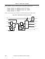
Internal Block Diagram ................................................................................................ 29
ARM 946E-S Processor System in ERTEC 400 ......................................................... 47
Revision_Code_and_Status Register ........................................................................ 61
Async_Wait_Cycle_Config Register ........................................................................... 62
SDRAM_Bank_Config Register (1/2) ........................................................................ 63
SDRAM_Refresh_Control Register ........................................................................... 65
Async_Bank(3:0)_Config Registers (1/2) .................................................................. 66
Extended_Config Register (1/2) ................................................................................ 68
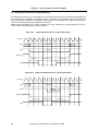
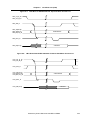
Write to External Device („Active Data Bus“)............................................................... 70
Read from External Device („Active Data Bus“) .......................................................... 70
Write to External Device Using RDY_PER_N („Active Data Bus“).............................. 71
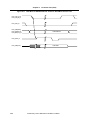
32-bit Write to External 8-bit Device („Active Data Bus“)............................................. 71
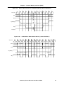
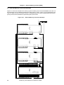
External Memory Connection Example ....................................................................... 72
IRVEC IRQ Interrupt Vector Register ......................................................................... 79
FIVEC FIQ Interrupt Vector Register .......................................................................... 80
LOCKREG IRQ Interrupt Priority Lock Register ......................................................... 81
FIQ1SREG Interrupt Select Register ......................................................................... 82
FIQ2SREG Interrupt Select Register ......................................................................... 83
IRQACK IRQ Interrupt Acknowledge Register ........................................................... 84
FIQACK FIQ Interrupt Acknowledge Register ............................................................ 85
IRCLVEC IRQ Interrupt Request Clear Register ........................................................ 86
MASKALL Mask All IRQ Interrupt Request Register .................................................. 86
IRQEND End of IRQ Interrupt Signaling Register ...................................................... 87
FIQEND End of FIQ Interrupt Signaling Register ....................................................... 87
FIQPR0...7 FIQ Interrupt Priority Register .................................................................. 88
FIQISR FIQ Interrupt In-Service Register ................................................................... 88
FIQIRR FIQ Interrupt Request Register ..................................................................... 89
FIQ_MASKREG FIQ Interrupt Mask Register ............................................................ 89
IRREG IRQ Interrupt Request Register ..................................................................... 90
MASKREG IRQ Interrupt Mask Register .................................................................... 90
ISREG IRQ Interrupt In-Service Register ................................................................... 91
TRIGREG IRQ Trigger Mode Select Register ............................................................ 91
EDGEREG IRQ Trigger Edge Select Register ........................................................... 92
SWIRREG Software IRQ Interrupt Register ............................................................... 92
PRIOREG0-15 IRQ Interrupt Priority Register ........................................................... 93
PCI Interrupt Handling ................................................................................................. 97
Example for LBU Address Line Connection .............................................................. 108
LBU Read from ERTEC 400 with Separate Read Control Line................................. 110
LBU Write to ERTEC 400 with Separate Write Control Line ..................................... 111
LBU Read from ERTEC 400 with Common Read/Write Control Line ....................... 111
LBU Write to ERTEC 400 with Common Read/Write Control Line............................ 112
LBU Page Range Register Low (LBU_Pn_RG_L) ................................................... 114
LBU Page Range Register High (LBU_Pn_RG_H) .................................................. 114
LBU Page Offset Register Low (LBU_Pn_OF_L) ..................................................... 115
LBU Page Offset Register High (LBU_Pn_OF_H) ................................................... 115
LBU Page Configuration Register (LBU_Pn_CFG) .................................................. 116
GPIO Cells of ERTEC 400 ........................................................................................ 119
GPIO_IOCTRL Register ........................................................................................... 121
GPIO_OUT Register ................................................................................................ 121
GPIO_IN Register .................................................................................................... 122
GPIO_PORT_MODE_L Register ............................................................................. 123
GPIO_PORT_MODE_H Register ............................................................................. 124
UART1/2 Macro Block Diagram ................................................................................ 128
UARTDR1/2 Data Register ...................................................................................... 131
Preliminary User’s Manual A17812EE1V1UM00
11
Figure 12-3:
Figure 12-4:
Figure 12-5:
Figure 12-6:
Figure 12-7:
Figure 12-8:
Figure 12-9:
Figure 13-1:
Figure 13-2:
Figure 13-3:
Figure 13-4:
Figure 13-5:
Figure 13-6:
Figure 13-7:
Figure 13-8:
Figure 14-1:
Figure 15-1:
Figure 15-2:
Figure 15-3:
Figure 15-4:
Figure 15-5:
Figure 15-6:
Figure 15-7:
Figure 15-8:
Figure 15-9:
Figure 15-10:
Figure 15-11:
Figure 15-12:
Figure 16-1:
Figure 16-2:
Figure 16-3:
Figure 16-4:
Figure 16-5:
Figure 16-6:
Figure 16-7:
Figure 16-8:
Figure 16-9:
Figure 17-1:
Figure 17-2:
Figure 17-3:
Figure 17-4:
Figure 17-5:
Figure 17-6:
Figure 17-7:
Figure 17-8:
Figure 17-9:
Figure 17-10:
Figure 17-11:
Figure 17-12:
Figure 17-13:
Figure 17-14:
Figure 17-15:
Figure 17-16:
Figure 17-17:
Figure 17-18:
Figure 17-19:
Figure 17-20:
Figure 17-21:
UARTRSR/UARTECR1/2 Registers ......................................................................... 132
UARTLCR_H1/2 Registers (1/2) .............................................................................. 133
UARTLCR_M1/2 Register ........................................................................................ 134
UARTLCR_L1/2 Register ......................................................................................... 135
UARTCR1/2 Registers (1/2) ..................................................................................... 135
UARTFR1/2 Registers (1/2) ..................................................................................... 137
UARTIIR/UARTICR1/2 Registers ............................................................................. 139
Block Diagram of SPI Interface ................................................................................. 142
SSPCR0 SPI Control Register 0 (1/2) ...................................................................... 144
SSPCR1 SPI Control Register 1 (1/2) ...................................................................... 146
SSPDR SPI Rx/Tx FIFO Data Register .................................................................... 147
SSPSR SPI Status Register ..................................................................................... 148
SSPCPSR SPI Clock Prescale Register .................................................................. 149
SSPIIR/SSPICR SPI Interrupt Identification and Clear Register .............................. 149
Connection of Serial Flash Memory to ERTEC 400 SPI Interface ............................ 150
PHY Connection via RMII Example........................................................................... 153
Simplified Block Diagram of Timers 0 and 1.............................................................. 155
Control/Status Register 0 (CTRL_STAT0) (1/2) ....................................................... 157
Control/Status Register 1 (CTRL_STAT1) (1/2) ....................................................... 159
Reload Register for Timer 0 (RELD0) ...................................................................... 161
Reload Register for Timer 1 (RELD1) ...................................................................... 161
Control Register for Prescaler 0 and 1 (CTRL_PREDIV) (1/2) ................................. 162
Reload Register for Prescaler 0 and 1 (RELD_PREDIV) ......................................... 163
Current Timer Value Register for Timer 0 (TIM0) ..................................................... 164
Current Timer Value Register for Timer 1 (TIM1) ..................................................... 164
F-Timer Block Diagram ............................................................................................. 165
F-Timer Counter Value Register (F-Counter-Val) ..................................................... 166
F-Timer Counter Reset Register (F-Counter-Res) ................................................... 166
Watchdog Timer Block Diagram................................................................................ 167
Watchdog Timer Output Timing ................................................................................ 168
Watchdog Control/Status Register (CTRL/STATUS) (1/2) ....................................... 170
Reload Register Low for Watchdog 0 (RELD0_LOW) .............................................. 171
Reload Register High for Watchdog 0 (RELD0_HIGH) ............................................ 172
Reload Register Low for Watchdog 1 (RELD1_LOW) .............................................. 172
Reload Register High for Watchdog 1 (RELD1_HIGH) ............................................ 173
Counter Register for Watchdog 0 (WDOG0) ............................................................ 173
Counter Register for Watchdog 1 (WDOG1) ............................................................ 173
Device Identification Register (ID_REG) .................................................................. 176
Boot Mode Pin Register (BOOT_REG) .................................................................... 176
Config Pin Register (CONFIG_REG) ....................................................................... 177
Reset Control Register (RES_CTRL_REG) (1/2) ..................................................... 177
Reset Status Register (RES_STAT_REG) ............................................................... 179
PLL Status Register (PLL_STAT_REG) (1/3) .......................................................... 180
Clock Control Register (CLK_CTRL_REG) .............................................................. 182
PCI Power State Request Register (PM_STATE_REQ_REG) ................................ 183
PCI Power State Acknowledge Register (PM_STATE_ACK_REG) ......................... 183
PME Register (PME_REG) ...................................................................................... 184
AHB Timeout Address Register (QVZ_AHB_ADR) .................................................. 184
AHB Timeout Control Signal Register (QVZ_AHB_CTRL) ....................................... 185
AHB Timeout Master Register (QVZ_AHB_M) ......................................................... 186
APB Timeout Address Register (QVZ_APB_ADR) .................................................. 187
EMIF Timeout Address Register (QVZ_EMIF_ADR) ............................................... 187
PCI Reset Request Register (PCI_RES_REQ) ........................................................ 188
PCI Reset Acknowledge Register (PCI_RES_ACK) ................................................ 189
Memory Swap Register (MEM_SWAP) .................................................................... 189
PCI Interrupt Control Register (PCI_INT_CTRL) ...................................................... 190
AHB Master Lock Control Register (M_LOCK_CTRL) ............................................. 191
ARM9 Control Register (ARM9_CTRL) (1/2) ........................................................... 192
Preliminary User’s Manual A17812EE1V1UM00
12
Figure 17-22:
Figure 18-1:
Figure 18-2:
Figure 19-1:
Figure 21-4:
13
ARM9 Control Write Enable Register (ARM9_WE) .................................................. 193
Detailed Representation of Clock Unit....................................................................... 196
Clock Supply of Ethernet Interface ............................................................................ 198
PLL Power-up Phase................................................................................................. 199
JTAG Connector Pin Assignment.............................................................................. 208
Preliminary User’s Manual A17812EE1V1UM00
14
Preliminary User’s Manual A17812EE1V1UM00
List of Tables
Table 1-1:
Table 1-2:
Table 2-1:
Table 2-2:
Table 2-3:
Table 2-4:
Table 2-5:
Table 2-6:
Table 2-7:
Table 2-8:
Table 2-9:
Table 2-10:
Table 2-11:
Table 2-12:
Table 2-13:
Table 2-14:
Table 2-15:
Table 3-1:
Table 4-1:
Table 5-1:
Table 5-2:
Table 5-3:
Table 6-1:
Table 6-2:
Table 7-1:
Table 7-2:
Table 7-3:
Table 8-1:
Table 8-2:
Table 8-3:
Table 9-1:
Table 9-2:
Table 9-3:
Table 9-4:
Table 9-5:
Table 9-6:
Table 9-7:
Table 9-8:
Table 10-1:
Table 11-1:
Table 11-2:
Table 11-3:
Table 12-1:
Table 12-2:
Table 12-3:
Table 12-4:
Table 12-5:
Table 13-1:
Table 13-2:
Table 13-3:
Table 14-1:
Table 14-2:
Table 15-1:
Table 15-2:
Table 15-3:
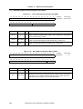
Pin Configuration of ERTEC 400.................................................................................... 22
Pin Identification ............................................................................................................. 27
External Memory Interface Pin Functions....................................................................... 33
PCI Interface Pin Functions............................................................................................ 34
Local Bus Interface Pin Functions .................................................................................. 35
RMII Interface Pin Functions .......................................................................................... 36
MII Interface Pin Functions............................................................................................. 37
General Purpose I/O Pin Functions................................................................................ 38
UART1 and UART2 Pin Functions ................................................................................. 39
SPI Pin Functions ........................................................................................................... 39
MC_PLL Pin Functions................................................................................................... 40
Clock and Reset Pin Functions ...................................................................................... 40
JTAG and Debug Interface Pin Functions ...................................................................... 40
Trace Port Pin Functions ................................................................................................ 41
Power Supply Pin Functions........................................................................................... 41
Pin Characteristics.......................................................................................................... 42
Pin Status During Reset and Recommended Connections............................................ 44
CP15 Coprocessor Registers ......................................................................................... 50
Possible AHB Master/slave Combinations ..................................................................... 52
Memory Area Partitioning ............................................................................................... 53
Detailed Description of Memory Segments .................................................................... 54
Memory Map and Used Address Range Example ......................................................... 56
External Memory Interface Pin Functions....................................................................... 59
External Memory Interface Control Registers................................................................. 61
FIQ Interrupt Sources .................................................................................................... 73
IRQ Interrupt Sources..................................................................................................... 74
Interrupt Control Registers ........................................................................................... 77
PCI Interface Pin Functions............................................................................................ 95
PCI Interrupt Routing...................................................................................................... 97
Address Assignment of PCI Registers ......................................................................... 100
Local Bus Interface Pin Functions ................................................................................ 103
Page Size Settings ....................................................................................................... 105
Page Offset Setting Examples...................................................................................... 106
Local Bus Unit Address Mapping Example .................................................................. 107
LBU Register Initialization Example ............................................................................. 108
32-bit Accesses in Various Address Ranges................................................................ 109
Possible Host Accesses to ERTEC 400 ....................................................................... 110
Address Assignment of LBU Registers ........................................................................ 113
Supported Download Modes ........................................................................................ 117
GPIO Pin and Related Drive Capabiliy......................................................................... 119
Address Assignment of GPIO Registers ...................................................................... 120
Alternative Functions of GPIO pins .............................................................................. 125
UART1/UART2 Pin Functions ...................................................................................... 127
Baud Rates and Tolerances for 50 MHz UART Operation Clock................................. 129
Address Assignment of UART1/2 Registers................................................................. 130
GPIO Register Initialization Example for Two-wire UARTs .......................................... 140
GPIO Register Initialization Example for Five-wire UARTs .......................................... 140
SPI Pin Functions ......................................................................................................... 141
Address Assignment of SPI Registers.......................................................................... 143
GPIO Register Initialization Example for External Serial Flash Memory ...................... 150
RMII Interface Pin Functions ........................................................................................ 152
MII Interface Pin Functions........................................................................................... 154
Address Assignment of Timer 0 and Timer 1 Registers ............................................... 157
F-Timer Pin Functions .................................................................................................. 165
Address Assignment of F-Timer Registers................................................................... 166
Preliminary User’s Manual A17812EE1V1UM00
15
Table 16-1:
Table 17-1:
Table 18-1:
Table 19-1:
Table 19-2:
Table 21-1:
Table 21-2:
Table 21-3:
16
Address Assignment of Watchdog Registers ............................................................... 169
Address Assignment of System Control Registers....................................................... 175
Overview of ERTEC 400 Clocks................................................................................... 195
BOOT(2:0) Pin Functions ............................................................................................. 201
CONFIG(4:0) Pin Functions ......................................................................................... 201
Memory Map Decode Regions in ETM9 on ERTEC 400 ............................................. 205
Trace Port Pin Functions .............................................................................................. 206
JTAG and Debug Interface Pin Functions .................................................................... 207
Preliminary User’s Manual A17812EE1V1UM00
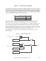
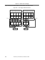
Chapter 1
Introduction
1.1 General
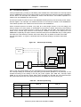
ERTEC 400 is a powerful communication block for development of industrial Ethernet devices.
ERTEC 400 contains a 32-bit RISC processor, an external memory interface with SDRAM and SRAM
controller, a PCI/LBU interface, a 4-channel real-time Ethernet interface, synchronous and asynchronous serial ports, and general purpose I/Os. Its robust construction, specific automation functions, and
openness to the IT world are distinguishing features. The ERTEC 400 is housed in a 304-pin plastic
FBGA package (19 mm × 19 mm).
(1)
ARM946E-S Processor
ERTEC 400 uses an ARM946E-S processor with configurable clock frequencies of 50, 100 or
150 MHz. This processor however, is based on the ARM9E-S core that supports the ARM5vTE
instruction set architecture with 32-bit wide normal instructions and the 16-bit wide THUMB
instruction set.
It includes support for separate instruction and data caches as well as tightly coupled memory. In
case of ERTEC 400 8 kBytes of instruction cache (I-cache) and 4 kBytes of data cache (D-cache)
are available. The tightly coupled memory (TCM) has a size of 4 kBytes and can be accessed with
full CPU speed.
An integrated memory protection unit (MPU) allows to restrict access permission to eight programmable portions of the ERTEC 400 address space.
The processor core is extended with two on-chip interrupt controllers, one of which is connected to
the core’s FIQ input while the other one is connected to the IRQ input. The IRQ interrupt controller
handles up to 16 interrupt sources that can be prioritized; the FIQ interrupt controller can handle
up to 8 sources. Most interrupt sources are assigned to internal peripheral units, however GPIO
pins can be used as interrupt sources as well.
For easy debugging, ERTEC 400 is equipped with an ETM9 debug and trace module. In addition
to the on-chip debug capabilities of the ARM946E-S core, the ETM9 module allows instruction and
data trace. The ETM9 cell can be operated in full rate mode, as long as the CPU core frequency is
50 or 100 MHz; otherwise, half-rate mode must be selected.
(2)
Bus System
ERTEC 400’s internal bus structure is made up of a multilayer AHB bus and an APB bus. Both run
at a maximum speed of 50 MHz.
The multilayer AHB bus offers multimaster capability and up to three simultaneous bus communication processes between masters and slaves. Thus a very high availability of the AHB bus is
achieved. Potential bus masters are the ARM core, the PCI/LBU interface and the IRT switch;
slaves are the external memory interface, the PCI interface, the IRT switch, interrupt controller,
on-chip SRAM and the AHB-to-APB bridge.
The APB bus connects to the less demanding peripherals like UARTs, SPI, GPIOs etc.
(3)
On-chip Memories
ERTEC 400 has two categories of on-chip memories: the caches and the data TCM that are
regarded as belonging to the core and SRAM as well as ROM that are on-chip, but off-core. The
on-chip SRAM has a size of 8 kBytes and an 32-bit organization. It is connected as an AHB slave
to the multilayer AHB bus and can be accessed with the full bus clock without wait states.
Additionally there are 8 kBytes of boot ROM that are implemented as an APB peripheral. The boot
ROM content is pre-defined and cannot be altered by the user. It contains a boot loader program
with the ability to choose among various other boot sources, if desired.
Preliminary User’s Manual A17812EE1V1UM00
17
Chapter 1 Introduction
(4)
External Memory Interface
The memory controller on ERTEC 400 supports synchronous DRAM as well as static memories
like SRAM or Flash. Additionally, static peripherals can be connected.
For SDRAM a data bus width of 16 or 32 bits can be configured; the addressing capabilities allow
connection of up to 256 MBytes of SDRAM. SDRAM is accessed with the clock speed of the
multilayer AHB bus, therefore the maximum SDRAM speed is 50 MHz with a CAS-latency of 2.
For static devices 4 chip selects with an address range of 16 MBytes each are prepared. They are
independently configurable to 8-, 16- or 32-bit bus width and to individual access timings. Slow
peripherals are supported with a ready signal input and a timeout function. Static chip select 0 can
be used for an external boot device - typically a flash memory - as an alternative to using the boot
loader in the on-chip ROM.
(5)
IRT Switch
The IRT switch block provides 4 Ethernet channels for 10 or 100 Mbps respectively half or full
duplex operation. The IRT switch is connected to the multilayer AHB bus as a master and a slave
and to the external world via a 4-channel RMII interface, that can be re-configured to 2-channel
MII operation. A large internal Communication SRAM with 192 kBytes in size helps to support RT
and IRT data communication over Ethernet.
(6)
PCI Interface
For easy integration into a PC-style environment respectively for easy connection to PC peripherals, ERTEC 400 has a 32-bit/66 MHz PCI interface that conforms to the PC specification R2.2 and
to the PCI Power Management specification V1.1. The PCI interface can be master or slave to the
multilayer AHB bus and master or target to the PCI bus. Host bridge functionality is implemented
and the interface can work in 3.3 V and 5 V environments.
(7)
Local Bus Unit
The PCI interface shares its pins with the Local Bus unit (LBU), that allows to run ERTEC 400 as a
peripheral to an external host controller. The LBU is a master to the multilayer AHB bus and has
separate address (21-bit) and data (16-bit) buses to the external world. Seen with the eyes of the
external host, the LBU opens a total of four configurable windows into the ERTEC 400, that allow
to configure ERTEC 400 and to access all internal resources.
(8)
Other Peripherals
The ERTEC 400 has several additional communication interfaces that can be accessed over the
AHB-to-APB bridge and the subsequent APB bus. These are two widely 16550-compatible
UARTs, an SPI channel, two timers, a watchdog, an additional fail-safe timer (F-timer) and a GPIO
block with up to 32 individually configurable I/Os. The interfaces share their pins with the GPIOs,
so that depending on the selected configuration a reduced number of GPIOs is available. 4 GPIOs
can be used as interrupt sources.
(9)
Clock and Power Supply
The ERTEC 400 can be operated with a single, external 12.5 MHz crystal. An internal oscillator
and PLL generate all required clocks for the ARM946E-S, the IRT block, the internal buses and
other peripherals. Alternatively, an external reference clock of 50 MHz can be supplied.
Two supply voltages are required for operation of ERTEC 400: The internal logic is running at
1.5 V and I/Os are operating at 3.3 V. The PCI interface has 5 V compatible I/Os.
18
Preliminary User’s Manual A17812EE1V1UM00
Chapter 1
Introduction
1.2 Device Features
• ARM946E-S Processor
-
Adjustable operating frequency (50/100/150 MHz)
System control co-processor (CP15)
4 kBytes of Data-TCM
Interface with “Write buffer” on 32-bit multilayer AHB bus
8 kBytes I-cache and 4 kBytes D-cache with lock functionality
Memory Protection Unit
Cacheability attribute setting for regions
Read/write access rights for certain modes only
2 interrupt controllers with 16 inputs for IRQ and 8 inputs for FIQ
Debug/trace functionality by ETM9 module via JTAG interface
Trace in full rate mode at operating frequencies of 50 and 100 MHz
Trace in half rate mode at an operating frequency of 150 MHz
4-/8-bit trace data width selectable
Trace can be restricted to selected address ranges and memory regions
• External Memory Interface (EMIF)
• SDRAM memory controller
- Adjustable 16-/32-bit data bus width
- PC100 SDRAM-compatible (50 MHz clock frequency)
- Maximum of 256 MBytes/32-bit or 128 Mbytes/16-bit SDRAM
- Adjustable RAS/CAS latency (2, 3 for Write; 1, 2 for Read)
- 2-bit bank address (1/2/4 banks) via address bits A1 and A0
- 8-/9/-10-/11-bit column address A13, A(11:2)
- Maximum 13-bit row address A(14:2)
• Asynchronous memory controller for SRAM, Flash, I/O
- Adjustable 8-/16-/32-bit data bus width
- 4 chip selects with individual timing control for each chip select
- Default setting for boot operation timing is “slow”
- Maximum of 16 Mbytes can be addressed for each chip select
- Chip select CS_PER0_N can be used for boot memory
- Data bus width of boot ROM at CS_PER0_N is selectable via BOOT(2:0) pins
- Adjustable timeout monitoring
- DTR_N (direction) and OE_DRIVER_N (enable) control signals for direct control of an
external driver for chip select signals CS_PER(3:0)_N
• IRT Switch
-
4 Fast Ethernet ports
10/100 Mbps and full duplex/half duplex mode support
Supports RT and IRT data traffic
Autonegotiation
Broadcast filter
IEEE 1588 time stamping
192 kBytes of Communication SRAM
Preliminary User’s Manual A17812EE1V1UM00
19
Chapter 1 Introduction
• PCI Interface
-
Host bridge functionality
Master/target functions
32-bit/66 MHz PCI bus
32-bit AHB bus
PCI configuration registers (can be initialized from ARM946E-S side)
Power Management V1.1
PCI interrupt outputs INTA_N, INTB_N and SERR_N
PCI segment of max. 2 GBytes can be addressed
3.3 V interface (5 V compatible)
Fully compatible with PCI Local Bus Specification 2.2
• Local Bus Unit (LBU)
-
16-bit data bus width, 21-bit address bus width
Host access to LBU paging registers via chip select signal LBU_CS_R_N
Host access to any address area of ERTEC 400 via chip select signal LBU_CS_M_N
Maximum of 4 pages can be addressed
Adjustable page-range and page-offset for each page; reconfigurable at any time
• Other I/O Interfaces
• 32-bit General Purpose I/O (GPIO)
- Input/outputs can be assigned on a bit-by-bit basis
- All GPIO equipped with internal pull-up resistor
- 4 GPIO inputs are interruptible (active Low level is not a supported interrupt level)
- GPIOs can be assigned up to 4 different functions (see Table 2-6)
- 8-/16-/32-bit access to registers is possible
• UART 1 and 2
- Based on ARM PrimeCell UART PL010 and widely 16550 compatible
• SPI
- Supports Motorola SPI, TI SSI and National Instruments microwire modes
- Programmable data frame size and bit rate
- Master and slave mode capability
- Send and Receive FIFOs with 8 16-bit entries
- Group and overrun error interrupts
• Timers
- Two 32-bit down counters with load/reload capability
- Start, stop, continue functions and interrupts
- Cascadable to a 64-bit timer and additional 8-bit prescaler selectable
- Timers run on 50 MHz internal clock
- Additional 32-bit fail-safe F-Timer
- Runs from external clock F_CLK
• Watchdog
- 32-bit count-down watchdog 0 with output pin WDOUT0_N
- 36-bit count-down watchdog 1
- Load/reload function
- Write protection for watchdog
- Watchdog interrupt on the FIQ interrupt controller
20
Preliminary User’s Manual A17812EE1V1UM00
Chapter 1
Introduction
1.3 Ordering Information
Device
Part Number
µPD800232F1-012-HN2
ERTEC 400
µPD800232F1-012-HN2-A
Remark:
Package
P-FBGA304, 19 × 19 mm
Products with -A at the end of the part number are lead-free products.
Preliminary User’s Manual A17812EE1V1UM00
21
Chapter 1 Introduction
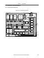
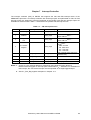
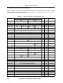
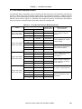
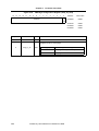
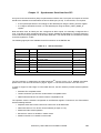
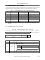
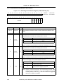
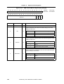
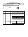
1.4 Pin Configuration
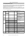
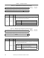
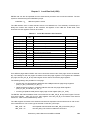
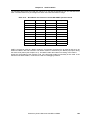
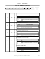
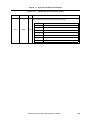
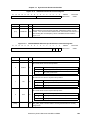
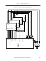
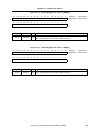
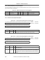
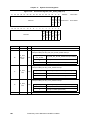
Figure 1-1:
Pin Configuration of ERTEC 400 - 304-Pin Plastic FBGA (19 mm × 19 mm)
22
21
20
19
18
17
16
15
14
13
12
11
10
9
8
7
6
5
4
3
2
1
AA W U R N L J G E C A
AB Y V T P M K H F D B
INDEX MARK
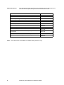
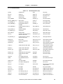
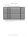
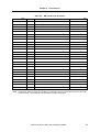
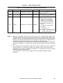
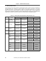
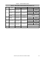
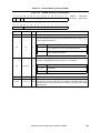
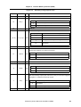
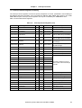
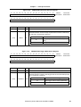
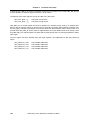
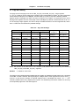
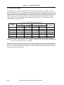
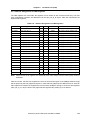
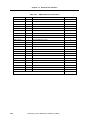
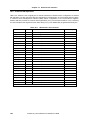
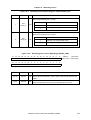
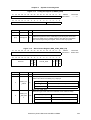
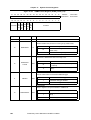
Table 1-1:
Pin
Number
22
Pin Name
Pin Configuration of ERTEC 400 (1/5)
Pin
Number
Pin Name
A2
AD01/LBU_DB01
A21
GND IO
A3
VDD IO
B1
A0
A4
AD07/LBU_DB07
B2
AD02/LBU_DB02
A5
VDD IO
B3
AD03/LBU_DB03
A6
AD12/LBU_DB12
B4
AD05/LBU_DB05
A7
GND IO
B5
AD08/LBU_DB08
A8
VDD IO
B6
AD10/LBU_DB10
A9
PERR_N/LBU_RD_N
B7
AD14/LBU_DB14
A10
IRDY_N/LBU_AB03
B8
CBE1_N/LBU_BE1_N
A11
VDD IO
B9
SERR_N/LBU_POL_RDY
A12
FRAME_N/LBU_AB04
B10
DEVSEL_N/LBU_AB01
A13
CBE2_N/LBU_AB05
B11
VDD Core
A14
AD19/LBU_AB09
B12
AD16/LBU_AB06
A15
VDD IO
B13
AD17/LBU_AB07
A16
CBE3_N/LBU_AB15
B14
AD21/LBU_AB11
A17
AD27/LBU_AB19
B15
AD23/LBU_AB13
A18
VDD IO
B16
AD25/LBU_AB17
A19
REQ_N/LBU_CS_M_N
B17
AD29/LBU_SEG_0
A20
VDD IO
B18
AD31/LBU_CS_R_N
Preliminary User’s Manual A17812EE1V1UM00
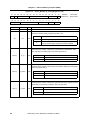
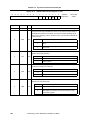
Chapter 1
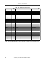
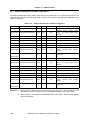
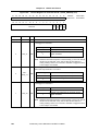
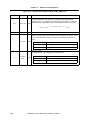
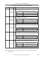
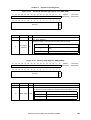
Table 1-1:
Pin
Number
Pin Name
Introduction
Pin Configuration of ERTEC 400 (2/5)
Pin
Number
Pin Name
B19
CLK_PCI
E15
P5V_PCI
B20
INTB_N/LBU_IRQ1_N
E16
GND IO
B21
RXD_P3(1)/RXD_P1(3)
E17
RES_PCI_N
B22
RXD_P3(0)/RXD_P1(2)
E18
VDD Core
C1
A2
E19
VDD Core
C2
A1
E21
RX_ER_P3/COL_P1
C21
TXD_P3(1)/TXD_P1(3)
E22
RXD_P2(1)/RXD_P1(1)
C22
TXD_P3(0)/TXD_P1(2)
F1
A7
D1
A4
F2
A6
D2
A3
F4
A16/BOOT0
D4
AD00/LBU_DB00
F5
A15
D5
AD04/LBU_DB04
F6
VDD Core
D6
VDD Core
F7
GND IO
D7
CBE0_N/LBU_BE0_N
F8
P5V_PCI
D8
AD09/LBU_DB09
F9
AD15/LBU_DB15
D9
VDD Core
F10
GND Core
D10
STOP_N/LBU_AB00
F13
GND IO
D11
TRDY_N/LBU_AB02
F14
AD24/LBU_AB16
D12
P5V_PCI
F15
AD28/LBU_AB20
D13
IDSEL/LBU_AB14
F16
GND Core
D14
AD30/LBU_SEG_1
F17
VDD Core
D15
VDD Core
F18
GND IO
D16
PME_N/LBU_RDY_N
F19
CRS_DV_P3/RX_DV_P1
D17
GNT_N/LBU_CFG
F21
RXD_P2(0)/RXD_P1(0)
D18
INTA_N/LBU_IRQ0_N
F22
AVDD_PCI
D19
M66EN
G1
A9
D21
TX_EN_P3/TX_ERR_P1
G2
A8
D22
VDD IO
G4
A17/BOOT1
E1
VDD IO
G5
GND IO
E2
A5
G6
GND Core
E4
A14
G17
GND Core
E5
VDD Core
G18
CRS_DV_P2/CRS_P1
E6
GND Core
G19
CRS_DV_P1/RX_DV_P0
E7
AD06/LBU_DB06
G21
AGND_PCI
E8
AD11/LBU_DB11
G22
TXD_P2(1)/TXD_P1(1)
E9
AD13/LBU_DB13
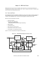
H1
A11
E10
PAR/LBU_WR_N
H2
A10
E11
AD18/LBU_AB08
H4
VDD Core
E12
AD20/LBU_AB10
H5
A20/CONFIG1
E13
AD22/LBU_AB12
H6
A19/CONFIG0
E14
AD26/LBU_AB18
H17
leave open
Preliminary User’s Manual A17812EE1V1UM00
23
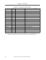
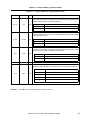
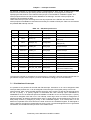
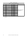
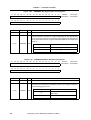
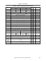
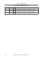
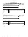
Chapter 1 Introduction
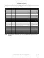
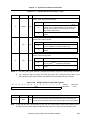
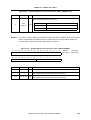
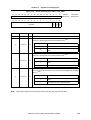
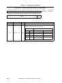
Table 1-1:
Pin
Number
24
Pin Name
Pin Configuration of ERTEC 400 (3/5)
Pin
Number
Pin Name
H18
RX_CLK_P1
N2
D0
H19
CRS_DV_P0/CRS_P0
N4
D18
H21
TXD_P2(0)/TXD_P1(0)
N5
VDD Core
H22
TX_EN_P2/TX_EN_P1
N6
D16
J1
A13
N17
GPIO4
J2
A12
N18
SMI_MDIO
J4
A18/BOOT2
N19
VDD Core
J5
A22/CONFIG3
N21
TXD_P0(1)/TXD_P0(1)
J6
A21/CONFIG2
N22
RXD_P0(0)/RXD_P0(0)
J17
TX_CLK_P1
P1
D1
J18
RX_ER_P2/RX_ER_P1
P2
D2
J19
VDD Core
P4
VDD Core
J21
RXD_P1(1)/RXD_P0(3)
P5
D19
J22
VDD IO
P6
GND IO
K1
RAS_SDRAM_N
P17
leave open
K2
CS_SDRAM_N
P18
VDD Core
K4
VDD Core
P19
GPIO5
K5
A23/CONFIG4
P21
TX_EN_P0/TX_EN_P0
K6
GND Core
P22
TXD_P0(0)/TXD_P0(0)
K17
TX_CLK_P0
R1
VDD IO
K18
RX_ER_P0/RX_ER_P0
R2
D3
K19
RX_CLK_P0
R4
D21
K21
RXD_P1(0)/RXD_P0(2)
R5
D22
K22
GND IO
R6
D20
L1
VDD IO
R17
GND IO
L2
CLK_SDRAM
R18
VDD Core
L4
CAS_SDRAM_N
R19
GPIO6
L5
BE2_DQM2_N
R21
RES_PHY_N
L18
GND Core
R22
REF_CLK
L19
VDD Core
T1
D4
L21
TXD_P1(1)/TXD_P0(3)
T2
D5
L22
TXD_P1(0)/TXD_P0(2)
T4
BE3_DQM3_N
M1
GND IO
T5
D23
M2
WE_SDRAM_N
T6
GND IO
M4
VDD Core
T17
GND Core
M5
D17
T18
GND IO
M18
SMI_MDC
T19
GPIO7
M19
TX_EN_P1/TX_ERR_P0
T21
GPIO0
M21
RXD_P0(1)/RXD_P0(1)
T22
VDD IO
M22
RX_ER_P1/COL_P0
U1
GND Core
N1
BE0_DQM0_N
U2
D6
Preliminary User’s Manual A17812EE1V1UM00
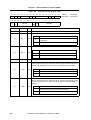
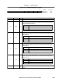
Chapter 1
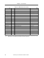
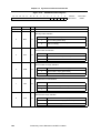
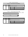
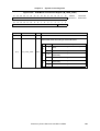
Table 1-1:
Pin
Number
Pin Name
Introduction
Pin Configuration of ERTEC 400 (4/5)
Pin
Number
Pin Name
U4
VDD Core
W7
VDD Core
U5
GND Core
W8
VDD Core
U6
VDD Core
W9
GPIO28
U7
GND Core
W10
GPIO27
U8
DTR_N
W11
AVDD
U9
GND Core
W12
CLKP_B
U10
AGND
W13
GPIO12/CTS1_N/ ETMEXTOUT
U13
GND Core
W14
VDD Core
U14
GND Core
W15
VDD Core
U15
GPIO14/RXD2
W16
GPIO15/DCD2_N/WDOUT0_N
U16
GND IO
W17
VDD Core
U17
VDD Core
W18
TDI
U18
GND Core
W19
TCK
U19
TMS
W21
DBGREQ
U21
GPIO1
W22
GPIO18/SSPRXD
U22
GND IO
Y1
VDD IO
V1
BE1_DQM1_N
Y2
D10
V2
D7
Y21
PIPESTA0
V4
D24
Y22
GPIO23/SCLKIN/DBGACK
V5
VDD Core
AA1
D11
V6
CS_PER3_N
AA2
D13
V7
GND IO
AA3
D15
V8
OE_DRIVER_N
AA4
D26
V9
GND Core
AA5
D28
V10
GPIO29
AA6
D30
V11
GPIO30
AA7
CS_PER1_N
V12
GPIO31
AA8
RDY_PER_N
V13
GND IO
AA9
WR_N
V14
VDD Core
AA10
GPIO25/TGEN_OUT1_N
V15
GPIO13/TXD2
AA11
GPIO24/PLL_EXT_IN_N
V16
TDO
AA12
F_CLK
V17
GND Core
AA13
CLKP_A
V18
VDD Core
AA14
GPIO17/CTS2_N/SSPOE
V19
TRST_N
AA15
RESET_N
V21
GPIO3
AA16
GPIO22/SFRMIN/TRACEPKT7
V22
GPIO2
AA17
GPIO20/SCLKOUT/TRACEPKT5
W1
D8
AA18
GPIO11/DSR1_N/TRACEPKT3
W2
D9
AA19
GPIO10/DCD1_N/TRACEPKT2
W4
D12
AA20
GPIO8/TXD1/TRACEPKT0
W5
D25
AA21
PIPESTA2
W6
CS_PER2_N
AA22
PIPESTA1
Preliminary User’s Manual A17812EE1V1UM00
25
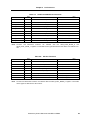
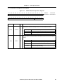
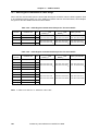
Chapter 1 Introduction
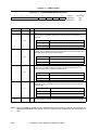
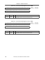
Table 1-1:
Pin
Number
26
Pin Name
Pin Configuration of ERTEC 400 (5/5)
Pin
Number
Pin Name
AB2
D14
AB12
TAP_SEL
AB3
VDD IO
AB13
GND IO
AB4
D27
AB14
GPIO16/DSR2_N/SSPCTLOE/ETMEXTIN1
AB5
D29
AB15
VDD IO
AB6
D31
AB16
TRACECLK
AB7
VDD IO
AB17
GPIO21/SFRMOUT/TRACEPKT6
AB8
CS_PER0_N
AB18
GPIO19/SSPTXD/TRACEPKT4
AB9
RD_N
AB19
VDD IO
AB10
GPIO26
AB20
GPIO9/RXD1/TRACEPKT1
AB11
VDD IO
AB21
TRACESYNC
Preliminary User’s Manual A17812EE1V1UM00
Chapter 1
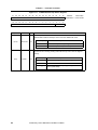
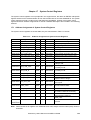
Introduction
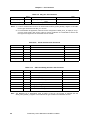
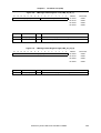
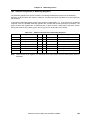
1.5 Pin Identification
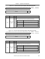
Table 1-2:
Pin Identification (1/2)
A(23:0)
: Address bus
PAR
: PCI parity
D(31:0)
: Data bus
SERR_N
: PCI system error
WR_N
: Write strobe
PERR_N
: PCI parity error
RD_N
: Read strobe
STOP_N
: PCI stop
CLK_SDRAM
: Clock to SDRAM
DEVSEL_N
: PCI device select
BE(3:0)_DQM(3:0)_N
: Byte enable
TRDY_N
: PCI target ready
CS_SDRAM_N
: Chip select to SDRAM
IRDY_N
: PCI initiator ready
RAS_SDRAM_N
: Row address strobe to
SDRAM
FRAME_N
: PCI cycle frame
CAS_SDRAM_N
: Column address strobe to
SDRAM
LBU_AB(20:0)
: LBU address bus
WE_SDRAM_N
: RD/WR SDRAM
LBU_DB(15:0)
: LBU data bus
CS_PER(3:0)_N
: Chip select
LBU_WR_N
: LBU write control
RDY_PER_N
: Ready signal
LBU_RD_N
: LBU read control
DTR_N
: Direction signal for external
driver or scan clock
LBU_BE(1:0)_N
: LBU byte enable
OE_DRIVER_N
: Enable signal for external
driver or scan clock
LBU_SEG_(1:0)
: LBU page selection
BOOT(2:0)
: Boot mode
LBU_IRQ_(1:0)_N
: LBU interrupt request
CONFIG(4:0)
: System configuration
LBU_RDY_N
: LBU ready signal
GPIO(31:0)
: GPIO pins
LBU_CS_M_N
: LBU chip select to ERTEC
400 internal resources
TXD(2:1)
: UART transmit data output
LBU_CS_R_N
: LBU chip select to page
configuration registers
RXD(2:1)
: UART receive data input
LBU_CFG
: LBU separate RD/WR
DCD(2:1)_N
: UART carrier detection
signal
LBU_POL_RDY
: LBU polarity selection for
pin LBU_RDY_N
DSR(2:1)_N
: UART data set ready signal
SSPRXD
: SPI receive data
CTS(2:1)_N
: UART transmit enable
signal
SSPTXD
: SPI transmit data
AD(31:0)
: PCI address data bits
SCLKOUT
: SPI clock out
IDSEL
: PCI initialization device
select
SFRMOUT
: SPI serial frame output
CBE(3:0)_N
: PCI byte enable
SFRMIN
: SPI serial frame input
PME_N
: PCI power management
SCLKIN
: SPI clock in
REQ_N
: PCI request
SSPCTLOE
: SPI clock and serial frame
output enable
GNT_N
: PCI grant
SSPOE
: SPI output enable
CLK_PCI
: PCI clock
TXD_P(3:0) 0
: (R)MII transmit data bit 0
RES_PCI_N
: PCI reset
TXD_P(3:0) 1
: (R)MII transmit data bit 1
INTA_N
: PCI interrupt INTA_N
TXD_P(1:0) 2
: MII transmit data bit 2
INTB_N
: PCI interrupt INTB_N
TXD_P(3:0) 3
: MII transmit data bit 3
M66EN
: PCI clock selection
RXD_P(3:0) 0
: (R)MII receive data bit 0
Preliminary User’s Manual A17812EE1V1UM00
27
Chapter 1 Introduction
Table 1-2:
Pin Identification (2/2)
RXD_P(3:0) 1
: (R)MII receive data bit 1
TRST_N
: JTAG reset
RXD_P(1:0) 2
: MII receive data bit 2
TCK
: JTAG clock
RXD_P(1:0) 3
: MII receive data bit 3
TDI
: JTAG data in
TX_EN_P(3:0)
: (R)MII transmit enable
TMS
: JTAG test mode select
TX_ERR_P(1:0)
: MII transmit error
TDO
: JTAG data out
CRS_DV_P(3:0)
: RMII carrier sense/data
valid
DBGREQ
: Debug request to ARM9
RX_ER_P(3:0)
: (R)MII receive error
DBGACK
: Debug acknowledge
CRS_P(1:0)
: MII carrier sense
TAP_SEL
: Select TAP controller
RX_DV_P(1:0)
: MII receive data valid
CLKP_A
: Quartz connection
COL_P(1:0)
: MII collision
CLKP_B
: Quartz connection
RX_CLK_P(1:0)
: MII receive clock
REF_CLK
: Reference clock input
TX_CLK_P(1:0)
: MII transmit clock
F_CLK
: Clock for F-counter
SMI_MDC
: (R)MII SMI clock
RESET_N
: HW reset
SMI_MDIO
: (R)MII SMI input/output
WDOUT0_N
: Watchdog output
RES_PHY_N
: Reset to PHY
VDD Core
: Power supply for core, 1.5 V
PLL_EXT_IN_N
MC_PLL input signal
GND Core
: GND for core
TGEN_OUT1_N
MC_PLL output signal
VDD IO
: Power supply for IO 3.3 V
TRACEPKT(7:0)
: Trace pins of ETM
GND IO
: GND for IO
ETMEXTOUT
: ETM output signal
P5V_PCI
: Power supply for PCI 5 V
ETMEXTIN1
: ETM input signal
AVDD
: Analog power Supply for
PLL, 1.5 V
PIPESTA(2:0)
: Trace pipeline status
AGND
: Analog GND for PLL
TRACESYNC
: Trace sync signal
AVDD_PCI
: Analog power supply for
PLL in PCI I/F, 1.5 V
TRACECLK
: ETM trace or scan clock
AGND_PCI
: Analog GND for PLL in PCI
I/F
28
Preliminary User’s Manual A17812EE1V1UM00
Chapter 1
Introduction
1.6 Configuration of Functional Blocks
1.6.1 Block Diagram of ERTEC 400
Figure 1-2:
Internal Block Diagram
External Memory Interface
Trace
Port
JTAG / Debug
74
12.5 MHz
REF_CLK
7
100 MHz
Slave
Slave
APB
Master
Slave
GPIO
Slave
Slave
Boot
ROM
(8 kBytes)
2 x UART
Slave
Slave
ETM
SPI
Interface
Slave
(EMIF)
50 MHz
I-Cache (8 kBytes)
D-Cache (4 kBytes)
D-TCM (4 kBytes)
50/100/150 MHz
2 x Timer,
Watchdog,
F-Timer
Slave
SRAM
(8 kBytes)
ARM
Interrupt
Controller
ARM9
Clock
BSTAP
with
External
Memory
Interface
Reset
Clock
Unit
ARM946E-S
System
Control
Register
(32 bit, 50 MHz)
Master
Local
Bus Unit
(LBU)
(16 bit)
Master
Multilayer AHB
(32 bit, 50 MHz)
Input
stage
MUX/Arb.
Master
Slave
AHBWrapper
AHBWrapper
Slave
Master
MC-Bus (32 bit, 50 MHz)
Slave
PCI
Bridge
32
MUX/Arb.
SC-Bus (32 bit, 50 MHz)
Communication
SRAM
Switch Control
(32 bit, 66 MHz)
Master/Targetcapable
(192 kBytes)
Ethernet
Channel
Ethernet
Channel
Ethernet
Channel
Ethernet
Channel
(Port 0)
(Port 1)
(Port 2)
(Port 3)
IRT
Switch
Macro
Peripheral Ports
Input
stage
AHB/APB
Bridge
Master
Input
stage
Decode
Slave
MUX/Arb.
MUX/Arb.
MUX/Arb.
2
MC_PLL
2
SMI
7
7
7
7
52
REF_CLK
Ports
(UART,
SPI,
WDT)
4 x RMII/
2 x MII
PCI/Local Bus
Preliminary User’s Manual A17812EE1V1UM00
29
Chapter 1 Introduction
1.6.2 On-chip Units
(1)
CPU (ARM946E-S)
ERTEC 400 uses an ARM946E-S 32-bit RISC processor core running at a maximum speed of
150 MHz. This core processes 32-bit instructions according to the ARM5v5TE instruction set
architecture as well as 16-bit wide THUMB instructions. Instruction throughput is increased using
a five-stage pipeline, 8 kBytes of I-cache, 4 kBytes of D-cache and 4 kBytes of D-TCM.
(2)
Multilayer AHB Bus
The Multilayer AHB bus is the data highway within ERTEC 400. It connects all major functional
blocks with a 32-bit, 50 MHz segmented bus structure, that is able to run three bus transfers in
parallel without blocking.
(3)
External Memory Interface
Access to external memories is provided with a double memory controller that supports
256 MBytes of standard SDRAM with an access speed of 50 MHz and a total of 64 MBytes of
static memory with one dynamic and four static chip select signals. The static chip select signals
can be used for SRAM, Flash and peripheral devices. External bus width is configurable to
16-/32-bit for SDRAM and 8-/16-/32-bit for the static portion of the interface. Access timings are
individually selectable for each chip select.
(4)
Internal SRAM
ERTEC 400 provides 8 kBytes of internal SRAM in a 32-bit organization; the SRAM can be
accessed with the multilayer AHB speed, i.e. 50 MHz.
(5)
Interrupt Controller
The ARM processor core on ERTEC 400 has a “normal” interrupt input (IRQ) and a fast interrupt
input (FIQ). With the on-chip interrupt controller, the interrupt processing capabilities are extended
to 16 IRQs and 8 FIQs with prioritization and vectorization. These interrupts are partly assigned to
internal resources and partly accessible to the external world via GPIO pins.
(6)
IRT Switch
The IRT switch block on ERTEC 400 provides four 10/100 Mbps Ethernet channels; due to special
control features and the large Communication SRAM of 192 kBytes, all channels support real-time
and isochronous real-time communication. Connection to an Ethernet network is realized with
external PHYs that are either wired to four RMII interfaces (4-channel operation) or two MII
interfaces (2-channel operation).
(7)
PCI Interface
ERTEC 400 has a 32-bit, 66 MHz PCI R2.2 compatible interface; host bridge functionality is
provided and the PCI clock is applied externally. On the PCI- bus side the interface can act as a
master or a target; on the AHB-side it can act as master or slave. The PCI configuration register
set can be programmed from PCI or AHB bus (i.e. ARM946E-S) side. The interface supports PCI
power management according to the V1.1 specification; 3.3 V and 5V PCI environments can be
used.
(8)
Local Bus Interface
The PCI interface pins are shared with a local bus interface (LBU) to an external host controller; it
offers 21 address bits and 16 data bits. ERTEC 400 is a slave with respect to this interface. The
external host can look through four configurable (in size and position) windows into ERTEC 400’s
address space. Read/write control is either done with separate read and write lines or with a
common read/write line.
30
Preliminary User’s Manual A17812EE1V1UM00
Chapter 1
(9)
Introduction
AHB to APB Bridge
The slower peripherals of ERTEC 400 are connected to an internal 32-bit/50 MHz APB bus that
can be accessed via an AHB-to-APB bridge from the AHB side. From the programmers point of
view, these peripherals are memory mapped like any other.
(10) Boot ROM
ERTEC 400 has 8 kBytes of 32-bit wide boot ROM; it is pre-defined with a boot-loader program
that supports various external boot sources: external Flash via EMIF, serial Flash or EEPROM via
SPI, PCI/LBU with an external host and UART1. Selection of boot sources is done via the
BOOT(2:0) configuration pins.
(11) GPIO Block
ERTEC 400 has a total of 32 GPIO pins that are individually programmable as input or output.
Four of these GPIOs can be used as interrupts. 16 of these GPIOs are shared with the UARTs and
the SPI.
(12) UART
Two identical UARTs can be used for asynchronous, serial communication. They are based on the
ARM prime cell PL010 and are widely 16550-compatible. 2 data lines and 3 handshake lines are
used. The internal 50 MHz clock is used for the UART operation and with a baud rate generator
standard baud rates up to 115 kbps can be selected.
(13) SPI
The SPI is used for synchronous serial communication according to Motorola, TI and National
quasi-standards. Frame size, protocol and speed are software programmable. The maximum
transmission speed is 25 MHz in master mode and 4.16 MHz in slave mode. The SPI is based on
the ARM prime cell PL021.
(14) Timers, Watchdog
ERTEC 400 has three timers and two watchdogs. Two of the timers are driven with the internal
50 MHz clock and based on 32-bit respectively 36-bit down counters that are cascadable and that
can be configured with an additional 8-bit prescaler. The third timer, the F-timer, runs under the
control of an external clock.
The watchdog timers are also based on 32-bit and 36-bit down-counters. Watchdog 0 (32-bit) is
generating an output signal on the WDOUT0_N pin; watchdog 1 (36-bit) generates a reset.
(15) System Control Registers
A bundle of specific system control registers help to configure the processor and to analyse
internal problems like access right and/or address range violations or timeouts.
Preliminary User’s Manual A17812EE1V1UM00
31
Chapter 1 Introduction
[MEMO]
32
Preliminary User’s Manual A17812EE1V1UM00
Chapter 2
Pin Functions
2.1 List of Pin Functions
Table 2-1:
Pin Name
External Memory Interface Pin Functions
I/O
Function
Alternate Function
A(23:19)
I/ONote
External memory address bus (23:19)
CONFIG(4:0)Note
A(18:16)
I/ONote
External memory address bus (18:16)
BOOT(2:0)Note
A(15:0)
O
External memory address bus (15:0)
-
D(31:0)
I/O
External memory data bus (31:0)
-
WR_N
O
Write strobe signal
-
RD_N
O
Read strobe signal
-
CLK_SDRAM
O
Clock to SDRAM
-
CS_SDRAM_N
O
Chip select to SDRAM
-
RAS_SDRAM_N
O
Row address strobe to SDRAM
-
CAS_SDRAM_N
O
Column address strobe to SDRAM
-
WE_SDRAM_N
O
RD/WR signal to SDRAM
-
CS_PER(3:0)_N
O
Chip select to static memories/peripherals
-
BE(3:0)_DQM(3:0)_N
O
Byte enable to static memories/peripherals and SDRAM -
RDY_PER_N
I
Ready signal from static peripherals
-
DTR_N
O
Direction signal for external driver or scan clock
-
OE_DRIVER_N
O
Enable signal for external driver or scan clock
-
Note: The BOOT(2:0) and CONFIG(4:0) pins used as inputs and read into the Boot_REG respectively
Config_REG system configuration registers during the active RESET phase. After a reset, these pins are
available as normal function pins and used as outputs
Preliminary User’s Manual A17812EE1V1UM00
33
Chapter 2 Pin Functions
Table 2-2:
Pin Name
PCI Interface Pin Functions
I/ONote
Function
Alternate FunctionNote
AD31
I/O
PCI address/data bit
LBU_CS_R_N
AD(30:29)
I/O
PCI address/data bits
LBU_SEG_(1:0)
AD(28:24)
I/O
PCI address/data bits
LBU_AB(20:16)
AD(23:16)
I/O
PCI address/data bits
LBU_AB(13:6)
AD(15:0)
I/O
PCI address data bits
LBU_DB(15:0)
PCI initialization device select
LBU_AB14
IDSEL
I
CBE3_N
I/O
PCI byte enable
LBU_AB15
CBE2_N
I/O
PCI byte enable
LBU_AB5
CBE1_N
I/O
PCI byte enable
LBU_BE1_N
CBE0_N
I/O
PCI byte enable
LBU_BE0_N
PME_N
I/O
PCI power management
LBU_RDY_N
REQ_N
O
PCI request
LBU_CS_M_N
GNT_N
I
PCI grant
LBU_CFG
CLK_PCI
I
PCI clock
-
RES_PCI_N
I
PCI reset
-
INTA_N
O
PCI INTA_N
LBU_IRQ0_N
INTB_N
O
PCI INTB_N
LBU_IRQ1_N
M66EN
I/O
PCI clock selection
-
PAR
I/O
PCI parity
LBU_WR_N
SERR_N
I/O
PCI system error
LBU_POL_RDY
PERR_N
I/O
PCI parity error
LBU_RD_N
STOP_N
I/O
PCI stop
LBU_AB0
DEVSEL_N
I/O
PCI device select
LBU_AB1
TRDY_N
I/O
PCI target ready
LBU_AB2
IRDY_N
I/O
PCI initiator ready
LBU_AB3
FRAME_N
I/O
PCI cycle frame
LBU_AB4
Note: PCI pins are alternatively used as local bus interface pins; in this table the I/O type is listed for the PCI
function.
34
Preliminary User’s Manual A17812EE1V1UM00
Chapter 2 Pin Functions
Table 2-3:
Pin Name
Local Bus Interface Pin Functions
I/ONote
Function
Alternate FunctionNote
LBU_AB(20:16)
I
LBU address bits
AD(28:24)
LBU_AB15
I
LBU address bit
CBE3_N
LBU_AB14
I
LBU address bit
IDSEL
LBU_AB(13:6)
I
LBU address bits
AD(23:16)
LBU_AB5
I
LBU address bit
CBE2_N
LBU_AB4
I
LBU address bit
FRAME_N
LBU_AB3
I
LBU address bit
IRDY_N
LBU_AB2
I
LBU address bit
TRDY_N
LBU_AB1
I
LBU address bit
DEVSEL_N
LBU_AB0
I
LBU address bit
STOP_N
LBU data bits
AD(15:0)
LBU_DB(15:0)
I/O
LBU_WR_N
I
LBU write control signal
PAR
LBU_RD_N
I
LBU read control signal
PERR_N
LBU_BE(1:0)_N
I
LBU byte enable
CBE(1:0)_N
LBU_SEG_(1:0)
I
LBU page selection signal
AD(30:29)
LBU_IRQ_1_N
O
LBU interrupt request signal
INTB_N
LBU_IRQ_0_N
O
LBU interrupt request signal
INTA_N
LBU_RDY_N
O
LBU ready signal
PME_N
LBU_CS_M_N
I
LBU chip select for ERTEC 400 internal resources
REQ_N
LBU_CS_R_N
I
LBU chip select for page configuration registers
AD31
LBU_CFG
I
LBU RD/WR control selection
GNT_N
LBU_POL_RDY
I
LBU polarity selection for LBU_RDY_N pin
SERR_N
Note: Local bus interface pins are alternatively used as PCI pins; in this table the I/O type is listed for the local
bus function.
Preliminary User’s Manual A17812EE1V1UM00
35
Chapter 2 Pin Functions
Table 2-4:
Pin NameNote
RMII Interface Pin Functions
I/O
Function
Alternate FunctionNote
SMI_MDC
O
SMI clock
SMI_MDC
SMI_MDIO
I/O
SMI input/output
SMI_MDIO
RES_PHY_N
O
Reset PHY
RES_PHY_N
TXD_P0(1:0)
O
Transmit Data Port 0 bits
TXD_P0(1:0)
RXD_P0(1:0)
I
Receive Data Port 0 bits
RXD_P0(1:0)
TX_EN_P0
O
Transmit Enable Port 0
TX_EN_P0
CRS_DV_P0
I
Carrier Sense/Data Valid Port 0
CRS_P0
RX_ER_P0
I
Receive Error Port 0
RX_ER_P0
TXD_P1(1:0)
O
Transmit Data Port 1 bits
TXD_P0(3:2)
RXD_P1(1:0)
I
Receive Data Port 1 bits
RXD_P0(3:2)
TX_EN_P1
O
Transmit Enable Port 1
TX_ERR_P0
CRS_DV_P1
I
Carrier Sense/Data Valid Port 1
RX_DV_P0
RX_ER_P1
I
Receive Error Port 1
COL_P0
TXD_P2(1:0)
O
Transmit Data Port 2 bits
TXD_P1(1:0)
RXD_P2(1:0)
I
Receive Data Port 2 bits
RXD_P1(1:0)
TX_EN_P2
O
Transmit Enable Port 2
TX_EN_P1
CRS_DV_P2
I
Carrier Sense/Data Valid Port 2
CRS_P1
RX_ER_P2
I
Receive Error Port 2
RX_ER_P1
TXD_P3(1:0)
O
Transmit Data Port 3 bits
TXD_P1(3:2)
RXD_P3(1:0)
I
Receive Data Port 3 bits
RXD_P1(3:2)
TX_EN_P3
O
Transmit Enable Port 3
TX_ERR_P1
CRS_DV_P3
I
Carrier Sense/Data Valid Port 3
RX_DV_P1
RX_ER_P3
I
Receive Error Port 3
COL_P1
Note: The alternate functions of RMII pins are MII pins; therefore some pin names are identical for both configurable functions. In this table I/O types are listed for the RMII configuration.
36
Preliminary User’s Manual A17812EE1V1UM00
Chapter 2 Pin Functions
Table 2-5:
Pin NameNote
MII Interface Pin Functions
I/O
Function
Alternate FunctionNote
SMI_MDC
O
Serial management interface clock
SMI_MDC
SMI_MDIO
I/O
Serial management interface data input/output
SMI_MDIO
RES_PHY_N
O
Reset signal to PHYs
RES_PHY_N
TXD_P0(3:2)
O
Transmit data port 0 bits
TXD_P1(1:0)
TXD_P0(1:0)
O
Transmit data port 0 bits
TXD_P0(1:0)
RXD_P0(3:2)
I
Receive data port 0 bits
RXD_P1(1:0)
RXD_P0(1:0)
I
Receive data port 0 bits
RXD_P0(1:0)
TX_EN_P0
O
Transmit enable port 0
TX_EN_P0
CRS_P0
I
Carrier sense port 0
CRS_DV_P0
RX_ER_P0
I
Receive error port 0
RX_ER_P0
TX_ERR_P0
O
Transmit error port 0
TX_EN_P1
RX_DV_P0
I
Receive data valid port 0
CRS_DV_P1
COL_P0
I
Collision port 0
RX_ER_P1
RX_CLK_P0
I
Receive clock port 0
-
TX_CLK_P0
I
Transmit clock port 0
-
TXD_P1(3:2)
O
Transmit data port 1 bits
TXD_P3(1:0)
TXD_P1(1:0)
O
Transmit data port 1 bits
TXD_P2(1:0)
RXD_P1(3:2)
I
Receive data port 1 bits
RXD_P3(1:0)
RXD_P1(1:0)
I
Receive data port 1 bits
RXD_P2(1:0)
TX_EN_P1
O
Transmit enable port 1
TX_EN_P2
CRS_P1
I
Carrier sense port 1
CRS_DV_P2
RX_ER_P1
I
Receive error port 1
RX_ER_P2
TX_ERR_P1
O
Transmit error port 1
TX_EN_P3
RX_DV_P1
I
Receive data valid port 1
CRS_DV_P3
COL_P1
I
Collision port 1
RX_ER_P3
RX_CLK_P1
I
Receive clock port 1
-
TX_CLK_P1
I
Transmit clock port 1
-
Note: The alternate functions of MII pins are RMII pins; therefore some pin names are identical for both configurable functions. In this table I/O types are listed for the MII configuration
Preliminary User’s Manual A17812EE1V1UM00
37
Chapter 2 Pin Functions
Table 2-6:
Pin Name
I/ONote
General Purpose I/O Pin Functions
Alternate FunctionNote
Function
GPIO(31:26)
I/O
General purpose I/O signal
-
GPIO25
I/O
General purpose I/O signal
TGEN_OUT1_N
GPIO24
I/O
General purpose I/O signal
PLL_EXT_IN_N
GPIO23
I/O
General purpose I/O signal
SCLKIN, DBGACK
GPIO22
I/O
General purpose I/O signal
SFRMIN, TRACEPKT7
GPIO21
I/O
General purpose I/O signal
SFRMOUT, TRACEPKT6
GPIO20
I/O
General purpose I/O signal
SCLKOUT, TRACEPKT5
GPIO19
I/O
General purpose I/O signal
SSPTXD, TRACEPKT4
GPIO18
I/O
General purpose I/O signal
SSPRXD
GPIO17
I/O
General purpose I/O signal
CTS2_N, SSPOE
GPIO16
I/O
General purpose I/O signal
DSR2_N, SSPCTLOE, ETMEXTIN1
GPIO15
I/O
General purpose I/O signal
DCD2_N, WDOUT0_N
GPIO14
I/O
General purpose I/O signal
RXD2
GPIO13
I/O
General purpose I/O signal
TXD2
GPIO12
I/O
General purpose I/O signal
CTS1_N, ETMEXTOUT
GPIO11
I/O
General purpose I/O signal
DSR1_N, TRACEPKT3
GPIO10
I/O
General purpose I/O signal
DCD1_N, TRACEPKT2
GPIO9
I/O
General purpose I/O signal
RXD1, TRACEPKT1
GPIO8
I/O
General purpose I/O signal
TXD1, TRACEPKT0
GPIO(7:0)
I/O
General purpose I/O signal
-
Note: Function and alternative functions are selected with the GPIO_PORT_MODE_H
GPIO_PORT_MODE_L registers. In this table the I/O types are listed for the GPIO function.
38
Preliminary User’s Manual A17812EE1V1UM00
and
Chapter 2 Pin Functions
Table 2-7:
Pin Name
UART1 and UART2 Pin Functions
I/ONote
Alternate FunctionNote
Function
TXD1
O
UART1 transmit data output
GPIO8, TRACEPKT0
RXD1
I
UART1 receive data input
GPIO9, TRACEPKT1
DCD1_N
I
UART1 carrier detection signal
GPIO10, TRACEPKT2
DSR1_N
I
UART1 data set ready signal
GPIO11, TRACEPKT3
CTS1_N
I
UART1 transmit enable signal
GPIO12, ETMEXTOUT
TXD2
O
UART2 transmit data output
GPIO13
RXD2
I
UART2 receive data input
GPIO14
DCD2_N
I
UART2 carrier detection signal
GPIO15, WDOUT0_N
DSR2_N
I
UART2 data set ready signal
GPIO16, SSPCTLOE, ETMEXTIN1
CTS2_N
I
UART2 transmit enable signal
GPIO17, SSPOE
Note: Function and alternative functions are selected with the GPIO_PORT_MODE_H and
GPIO_PORT_MODE_L registers. In this table the I/O types are listed for the UART1 and UART2 function.
Table 2-8:
Pin Name
I/ONote
SPI Pin Functions
Alternate FunctionNote
Function
SSPRXD
I
SPI receive data input
GPIO18
SSPTXD
O
SPI transmit data output
GPIO19, TRACEPKT4
SCLKOUT
O
SPI clock output
GPIO20, TRACEPKT5
SFRMOUT
O
SPI serial frame input signal
GPIO21, TRACEPKT6
SFRMIN
I
SPI serial frame output signal
GPIO22, TRACEPKT7
SCLKIN
I
SPI clock input
GPIO23, DBGACK
SSPCTLOE
O
SPI clock and serial frame output enable
GPIO16, DSR2_N, ETMEXTIN1
SSPOE
O
SPI output enable
GPIO17, CTS2_N
Note: Function and alternative functions are selected with the GPIO_PORT_MODE_H register. In this table
the I/O types are listed for the SPI function.
Preliminary User’s Manual A17812EE1V1UM00
39
Chapter 2 Pin Functions
Table 2-9: MC_PLL Pin Functions
Pin Name
I/ONote 1
Alternate FunctionNote 1
Function
PLL_EXT_IN_N
I
MC_PLL input signal
GPIO24
TGEN_OUT1_N
O
MC_PLL output signalNote 2
GPIO25
Notes: 1. Function and alternative functions are selected with the GPIO_PORT_MODE_H register. In this table
the I/O types are listed for the MC_PLL function.
2. For a PROFINET IRT application, GPIO25 must be configured as TGEN_OUT1_N output pin. A synchronous clock signal is then output at this pin; during certification of a PROFINET IO device with
IRT support this signal must be accessible from the outside.
Table 2-10:
Pin Name
Clock and Reset Pin Functions
I/O
Function
Alternate Function
TRACECLK
O
ETM trace or scan clock
-
CLKP_A
I
Quartz connection
-
CLKP_B
O
Quartz connection
-
F_CLK
I
F_CLK for F-counter
-
REF_CLK
I
Reference clock
-
RESET_N
I
Hardware reset
-
Table 2-11:
Pin Name
JTAG and Debug Interface Pin Functions
I/ONote
Function
TRST_N
I
JTAG reset signal
TCK
I
JTAG clock signal
TDI
I
JTAG data input signal
TMS
I
JTAG test mode select signal
TDO
O
JTAG data output signal
DBGREQ
I
Debug request signal
DBGACK
O
Debug acknowledge signal
TAP_SEL
I
TAP controller select signal
Alternate FunctionNote
GPIO23/SCLKIN
Note: The DBGACK pin is alternatively used as GPIO or SPI pin; the function is selected with the
GPIO_PORT_MODE_H register. In this table the I/O type is listed for the DBGACK function.
40
Preliminary User’s Manual A17812EE1V1UM00
Chapter 2 Pin Functions
Table 2-12:
Trace Port Pin Functions
I/ONote
Pin Name
Alternate FunctionNote
Function
TRACEPKT7
O
Trace packet bit
GPIO22/SFRMIN
TRACEPKT6
O
Trace packet bit
GPIO21/SFRMOUT
TRACEPKT5
O
Trace packet bit
GPIO20/SCLKOUT
TRACEPKT4
O
Trace packet bit
GPIO19/SSPTXD
TRACEPKT3
O
Trace packet bit
GPIO11/DSR1_N
TRACEPKT2
O
Trace packet bit
GPIO10/DCD1_N
TRACEPKT1
O
Trace packet bit
GPIO9/RXD1
TRACEPKT0
O
Trace packet bit
GPIO8/TXD1
PIPESTA(2:0)
O
CPU pipeline status
-
TRACESYNC
O
Trace sync signal
-
ETMEXTIN1
I
External input to the ETM
GPIO16/DSR2_N/SSPCTLOE
ETMEXTOUT
O
Output signal from the ETM
GPIO12/CTS1_N
Note: Several trace port pins are alternatively used as GPIO, UART or SPI pins; the function is selected with
the GPIO_PORT_MODE_H and GPIO_PORT_MODE_L registers. In this table the I/O types are listed
for the trace port pin functions.
Table 2-13: Power Supply Pin Functions
Pin Name
Function
VDD Core
Power supply for core, 1.5 V
GND Core
GND for core
VDD IO
Power supply for IO, 3.3 V
GND IO
GND for IO
P5V_PCI
Power supply for PCI, 5V Note
AVDD
Analog power supply for PLL, 1.5 V
AGND
Analog GND for PLL
AVDD_PCI
Analog power supply for PLL in PCI I/F, 1.5 V
AGND_PCI
Analog GND for PLL in PCI I/F
Note: In PCI mode the P5V_PCI pins must be connected to the PCI bus supply pins +VIO (name
according to PCI specification). In LBU mode the P5V_PCI pins must be connected to VDD IO.
Preliminary User’s Manual A17812EE1V1UM00
41
Chapter 2 Pin Functions
2.2 Pin Characteristics
Table 2-14:
Pin Name
A(23:16)
Pin Characteristics (1/2)
I/O
Input type
Output type
Internal pull
up/down
I/ONote 1
SchmittNote 1
3.3 V CMOS
Drive capability
IOH
IOL
-
9 mA
9 mA
A(15:0)
O
-
3.3 V CMOS
-
9 mA
9 mA
D(31:0)
I/O
Schmitt
3.3 V CMOS
50 kΩ pull up
9 mA
9 mA
WR_N
O
-
3.3 V CMOS
-
9 mA
9 mA
RD_N
O
-
3.3 V CMOS
-
9 mA
9 mA
CLK_SDRAM
O
-
3.3 V CMOS
-
9 mA
9 mA
CS_SDRAM_N
O
-
3.3 V CMOS
-
9 mA
9 mA
RAS_SDRAM_N
O
-
3.3 V CMOS
-
9 mA
9 mA
CAS_SDRAM_N
O
-
3.3 V CMOS
-
9 mA
9 mA
WE_SDRAM_N
O
-
3.3 V CMOS
-
9 mA
9 mA
CS_PER(3:0)_N
O
-
3.3 V CMOS
-
6 mA
6 mA
BE(3:0)_DQM(3:0)_N
O
-
3.3 V CMOS
-
9 mA
9 mA
RDY_PER_N
I
Schmitt
-
50 kΩ pull up
-
-
DTR_N
O
-
3.3 V CMOS
-
9 mA
9 mA
OE_DRIVER_N
O
-
3.3 V CMOS
-
9 mA
9 mA
AD(31:0)
I/O
PCINote 2
PCINote 2
-
I
PCINote 2
-
-
CBE(3:0)_N
I/O
PCINote 2
PCINote 2
-
PME_N
I/O
PCINote 2
PCINote 2
-
REQ_N
O
-
PCINote 2
-
GNT_N
I
PCINote 2
-
-
CLK_PCI
I
PCINote 2
-
-
RES_PCI_N
I
PCINote 2
-
-
INTA_N
O
-
PCINote 2
-
INTB_N
O
-
PCINote 2
-
M66EN
I
Schmitt
-
-
I/O
PCINote 2
PCINote 2
-
SERR_N
I/O
PCINote 2
PCI
Note 2
-
PERR_N
I/O
PCINote 2
PCINote 2
-
STOP_N
I/O
PCINote 2
PCINote 2
-
DEVSEL_N
I/O
PCINote 2
PCINote 2
-
TRDY_N
I/O
PCINote 2
PCINote 2
-
IRDY_N
I/O
PCINote 2
PCINote 2
-
FRAME_N
I/O
PCINote 2
PCINote 2
-
IDSEL
PAR
PCINote 2
-
-
PCINote 2
Notes: 1. The address pins A(23:16) are used as inputs only during the active reset phase.
2. PCI I/Os can be either 3.3 V PCI (if the PCI interface is operated with 3.3 V) or 5 V tolerant PCI
(if the PCI interface is configured to 5 V tolerant operation). Drive capability complies to the PCI
specification R2.2.
42
Preliminary User’s Manual A17812EE1V1UM00
Chapter 2 Pin Functions
Table 2-14:
Pin Characteristics (2/2)
I/O
Input type
Output type
Internal pull
up/down
PIPESTA(2:0)
O
-
3.3 V CMOS
TRACESYNC
O
-
3.3 V CMOS
SMI_MDC
O
-
SMI_MDIO
I/O
Pin Name
RES_PHY_N
Drive capability
IOH
IOL
-
9 mA
9 mA
-
9 mA
9 mA
3.3 V CMOS
-
6 mA
6 mA
Schmitt
3.3 V CMOS
-
6 mA
6 mA
O
-
3.3 V CMOS
-
6 mA
6 mA
Note 1
O
-
3.3 V CMOS
-
6 mA
6 mA
Note 1
RXD_Pn(1:0)
I
Schmitt
-
50 kΩ pull down
-
-
TX_EN_PnNote 1
O
-
3.3 V CMOS
-
6 mA
6 mA
CRS_DV_PnNote 1
I
Schmitt
-
50 kΩ pull down
-
-
RX_ER_Pn
I
Schmitt
-
50 kΩ pull down
-
-
TXD_Pn(3:0)Note 2
O
-
3.3 V CMOS
-
6 mA
6 mA
RXD_Pn(3:0)Note 2
I
Schmitt
-
50 kΩ pull down
-
-
O
-
3.3 V CMOS
-
6 mA
6 mA
CRS_PnNote 2
I
Schmitt
-
50 kΩ pull down
-
-
RX_ER_PnNote 2
I
Schmitt
-
50 kΩ pull down
-
-
O
-
3.3 V CMOS
-
6 mA
6 mA
RX_DV_PnNote 2
I
Schmitt
-
50 kΩ pull down
-
-
COL_PnNote 2
I
Schmitt
-
50 kΩ pull down
-
-
RX_CLK_PnNote 2
I
Schmitt
-
50 kΩ pull down
-
-
TX_CLK_PnNote 2
I
Schmitt
-
50 kΩ pull down
-
-
GPIO(31:23)
I/O
Schmitt
3.3 V CMOS
50 kΩ pull up
6 mA
6 mA
GPIO(22:19)
I/O
Schmitt
3.3 V CMOS
50 kΩ pull up
9 mA
9 mA
GPIO(18:12)
I/O
Schmitt
3.3 V CMOS
50 kΩ pull up
6 mA
6 mA
GPIO(11:0)
I/O
Schmitt
3.3 V CMOS
50 kΩ pull up
9 mA
9 mA
TRACECLK
O
-
3.3 V CMOS
-
18 mA
18 mA
CLKP_A
I
Osc. in
-
-
-
-
CLKP_B
O
-
Osc. out
-
6 mA
6 mA
F_CLK
I
3.3 V CMOS
-
-
-
-
REF_CLK
I
3.3 V CMOS
-
-
-
-
RESET_N
I
Schmitt
-
50 kΩ pull up
-
-
TRST_N
I
Schmitt
-
-
-
-
TCK
I
Schmitt
-
50 kΩ pull up
-
-
TDI
I
Schmitt
-
50 kΩ pull up
-
-
TMS
I
Schmitt
-
50 kΩ pull up
-
-
TDO
O
-
3.3 V CMOS
-
6 mA
6 mA
DBGREQ
I
Schmitt
-
50 kΩ pull down
-
-
TAP_SEL
I
Schmitt
-
50 kΩ pull up
-
-
TXD_Pn(1:0)
Note 1
TX_EN_Pn
Note 2
TX_ERR_Pn
Note 2
Notes: 1. The number “n” can take the integer values 0 to 3 and refers to the RMII ports.
2. The number “n” can take the integer values 0 and 1 and refers to the MII ports.
Remark:
Shared pins are not listed with all possible pin names. Please check Tables 2-1 to 2-12 for possible
pin names first, before looking up pin characteristics in Table 2-14.
Preliminary User’s Manual A17812EE1V1UM00
43
Chapter 2 Pin Functions
2.3 Pin Status and Recommended Connections
Table 2-15:
Pin Status During Reset and Recommended Connections (1/3)
I/O
Internal pull
up/down
I/O during
reset
Level
during reset
External pull
up/down required
A(23:16)
I/ONote 1
-
INote 1
-
Note 1
A(15:0)
O
-
O
L
-
D(31:0)
I/O
50 kΩ pull up
I
H
-
WR_N
O
-
O
H
-
Pin Name
RD_N
O
-
O
H
-
CLK_SDRAM
O
-
O
L
-
CS_SDRAM_N
O
-
O
H
-
RAS_SDRAM_N
O
-
O
H
-
CAS_SDRAM_N
O
-
O
H
-
WE_SDRAM_N
O
-
O
H
-
CS_PER(3:0)_N
O
-
O
H
-
BE(3:0)_DQM(3:0)_N
O
-
O
H
-
RDY_PER_N
I
50 kΩ pull up
I
H
-
DTR_N
O
-
O
H
-
OE_DRIVER_N
O
-
O
H
-
AD(31:0)
I/O
-
I
-
Pull upNote 2
I
-
I
-
Pull upNote 2
CBE(3:0)_N
I/O
-
I
-
Pull upNote 2
PME_NNote 3
I/O
-
I
H
Pull upNote 4
REQ_NNote 3
O
-
tri-state
-
Pull upNote 2, 4
GNT_NNote 3
I
-
I
-
Pull upNote 2, 4
CLK_PCINote 3
I
-
I
-
Pull downNote 2, 5
RES_PCI_N
I
-
I
-
Pull upNote 2, 4, 5
INTA_NNote 3
O
-
tri-state
H
Pull upNote 4
INTB_NNote 3
O
-
tri-state
H
Pull upNote 4
M66ENNote 3
I
-
I
-
Pull downNote 2, 5
PARNote 3
I/O
-
I
-
Pull upNote 2
SERR_NNote 3
I/O
-
I
H
Pull upNote 2, 4
PERR_NNote 3
I/O
-
I
-
Pull upNote 2, 4
STOP_NNote 3
I/O
-
I
-
Pull upNote 2, 4
IDSEL
Notes: 1. The address pins A(23:16) are used as inputs only during the active reset phase in order to read the
device’s proper start up configurations. A(23:16) must therefore be equipped with external pull up/
down resistors according to the desired start up configuration. Please consult the user’s manual for
details.
2. These resistors are required, when neither the PCI interface nor the LBU interface are used. In this
case ERTEC 400 must be configured to LBU mode (CONFIG2 = 0b).
3. The reset signal, that affects these pins, is RES_PCI_N.
4. These pull-up resistors are required, when the interface is operated in PCI mode.
5. These resistors are required, when the interface is operated in LBU mode.
44
Preliminary User’s Manual A17812EE1V1UM00
Chapter 2 Pin Functions
Table 2-15:
Pin Status During Reset and Recommended Connections (2/3)
I/O
Internal pull
up/down
I/O during
reset
Level
during reset
External pull
up/down required
DEVSEL_NNote 1
I/O
-
I
-
Pull upNote 2, 4
TRDY_NNote 1
I/O
-
I
-
Pull upNote 2, 4
IRDY_NNote 1
I/O
-
I
-
Pull upNote 2, 4
FRAME_NNote 1
I/O
-
I
-
Pull upNote 4
PIPESTA(2:0)
O
-
O
L
-
Pin Name
TRACESYNC
O
-
O
L
-
SMI_MDC
O
-
O
L
-
SMI_MDIO
I/O
-
I
H
Pull up
RES_PHY_N
O
-
O
L
-
TXD_Pn(1:0)Note 3
O
-
O
L
-
RXD_Pn(1:0)Note 3
I
50 kΩ pull down
I
L
-
TX_EN_PnNote 3
O
-
O
L
-
CRS_DV_PnNote 3
I
50 kΩ pull down
I
L
-
RX_ER_PnNote 3
I
50 kΩ pull down
I
L
-
TXD_Pn(3:0)Note 5
O
-
O
L
-
RXD_Pn(3:0)Note 5
I
50 kΩ pull down
I
L
-
TX_EN_PnNote 5
O
-
O
L
-
CRS_PnNote 5
I
50 kΩ pull down
I
L
-
RX_ER_PnNote 5
I
50 kΩ pull down
I
L
-
TX_ERR_PnNote 5
O
-
O
L
-
RX_DV_PnNote 5
I
50 kΩ pull down
I
L
-
COL_PnNote 5
I
50 kΩ pull down
I
L
-
RX_CLK_PnNote 5
I
50 kΩ pull down
I
L
-
TX_CLK_PnNote 5
I
50 kΩ pull down
I
L
-
GPIO(31:0)
I/O
50 kΩ pull up
I
H
-
TRACECLK
O
-
O
L
-
CLKP_A
I
-
I
-
-
CLKP_B
O
-
O
-
-
F_CLK
I
-
I
-
-
REF_CLK
I
-
I
-
-
RESET_N
I
50 kΩ pull up
I
LNote 6
-
Notes: 1. The reset signal, that affects these pins is RES_PCI_N.
2. These resistors are required, when neither the PCI interface nor the LBU interface are used. In this
case ERTEC 400 must be configured to LBU mode (CONFIG2 = 0b).
3. The number “n” can take the integer values 0 to 3.
4. These pull-up resistors are required, when the interface is operated in PCI mode.
5. The number “n” can take the integer values 0 and 1.
6. RESET_N must be externally driven low in order to reset the device.
Preliminary User’s Manual A17812EE1V1UM00
45
Chapter 2 Pin Functions
Table 2-15:
Pin Status During Reset and Recommended Connections (3/3)
I/O
Internal pull
up/down
I/O during
reset
Level
during reset
External pull
up/down required
TRST_N
I
-
I
HNote 1
Pull up
TCKNote 2
I
50 kΩ pull up
I
H
-
Pin Name
Note 2
I
50 kΩ pull up
I
H
-
TMSNote 2
I
50 kΩ pull up
I
H
-
TDONote 2
O
-
O
L
-
DBGREQ
I
50 kΩ pull down
I
L
-
TAP_SEL
I
50 kΩ pull up
I
H
-
TDI
Notes: 1. High level is generated from external pull up resistor and not by internal device circuitry.
2. The reset signal, that affects these pins, is TRST_N.
Remark:
46
Shared pins are not listed with all possible pin names. Please check Tables 2-1 to 2-13 for possible
pin names first, before looking up reset characteristics and recommended connections in
Table 2-15.
Preliminary User’s Manual A17812EE1V1UM00
Chapter 3
CPU Function
3.1 Structure of The ARM946E-S Processor System
An ARM946E-S processor system is used in ERTEC 400. Figure 3-1 shows the structure of the processor. In addition to the ARM9E-S processor core, the system contains a data cache, an instruction
cache, a memory protection unit (MPU), a system control co-processor, and a tightly coupled data
memory. The processor system has an interface to the integrated AHB bus.
Figure 3-1:
ARM 946E-S Processor System in ERTEC 400
ARM946E-S
I-Cache
D-Cache
D-TCM
I-Cache
control
D-Cache
control
TCM
control
Addr
{
IA
Dout
To/from AHB bus
system
AHB I/F
Din
ETM
I/F
DA
To/from
ETM
WData
Instr
ARM9E-S
RData
MPU
System
control
System control
coprocessor
(CP15)
External
coprocessor
I/F
To/from external
coprocessors
The ARM946E-S processor system is a member of the ARM9 Thumb family. It has a processor core
with Harvard architecture. Compared to the standard ARM9 family, the ARM946E-S has an enhanced
5vTE architecture permitting faster switching between ARM and Thumb code segments and an
enhanced multiplier structure. In addition, the processor has an integrated JTAG interface.
The processor can be operated at 50 MHz, 100 MHz or 150 MHz. The operating frequency is set during
the reset phase via the CONFIG3 and CONFIG4 configuration pins. Communication with the components of the ERTEC 400 takes place via the AHB bus at a frequency of 50 MHz.
Preliminary User’s Manual A17812EE1V1UM00
47
Chapter 3 CPU Function
3.2 Cache Structure of ARM946E-S
The following caches are integrated in the ARM946E-S processor system:
• 8 kBytes of instruction cache (I-cache) with lock function
• 4 kBytes of data cache (D-cache) with lock function
Both caches are 4-way set associative and have 1-kByte segments. Each segment consists of 32 lines
with 32 Bytes (8 x 4 Bytes). The D-cache has a write buffer with write-back function.
The lock function enables the user to “freeze” the contents of the cache segments. This function allows
the code for fast routines to be kept permanently in the I-cache. This mechanism can only be implemented on a segment-specific basis in the ARM946E-S.
Both caches are locked after a reset. The caches can be enabled only if the memory protection unit is
enabled at the same time. The I-cache can be enabled by setting Bit 12 of the CP15 control register;
the D-cache can be enabled by setting Bit 2 of the CP15 control register. Access to this area is blocked
if the cache is not enabled. When enabled, the caches can be accessed with the full CPU speed, i.e.
with a maximum of 150 MHz.
3.3 Tightly Coupled Memories
A 4-kBytes data TCM (D-TCM) is implemented in the ARM946E-S processor of ERTEC 400. A TCM is
a (mostly) small portion of memory that is close to the core, that can be accessed with full CPU speed,
but that is not subjected to automatic control mechanisms like a cache. It is typically used to keep the
data for time-critical routines.
The D-TCM is locked after a reset; it can be mapped to various positions in the address space of the
ARM946E-S and must be used together with a region of the memory protection unit. The D-TCM can
be enabled by setting Bit 16 of the CP15 control register. In addition, the address position of the D-TCM
must be set in the Tightly-Coupled Memory Region register.
48
Preliminary User’s Manual A17812EE1V1UM00
Chapter 3
CPU Function
3.4 Memory Protection Unit (MPU)
The memory protection unit enables the user to partition the address space of the ARM946E-S processor into several regions and to assign various attributes to these regions.
A maximum of 8 regions of variable size can be set. If regions overlap, the attributes of the higher
region number apply. The possible settings for each region are as follows:
• Base address of region
• Size of region
• Cache and “write buffer” configuration
• Read/write access enable for privileged users/users
They have to be made in the following registers of the ARM946E-S:
• Register 2: Cache configuration register”
• Register 3: Write buffer control register”
• Register 5: Access permission register”
• Register 6: Protection region/base size register”
The base address defines the start address of the region. It must always be a multiple of the size of the
region.
Example: The region size is 4 kBytes. The starting address is then always a multiple of 4 kBytes.
Before the MPU is enabled, at least one region must have been specified. Otherwise, the ARM946E-S
can enter a state that can only be cancelled by a reset. The MPU can be enabled by setting Bit 0 of the
CP15 control register. If the MPU is locked, neither the I-cache nor the D-cache can be accessed even
if they are enabled.
3.5 Bus Interface of ARM946E-S
The ARM946E-S uses an AHB bus master interface to the multilayer AHB bus for opcode fetches and
data transfers. The interface operates at a fixed frequency of 50 MHz, independently of the CPU
frequency. The two uni-directional data buses and the address bus each have a width of 32 bits. The
AHB bus supports burst transfers that are typically used during cache operations.
To improve system performance, the AHB bus master interface contains a write buffer that reduces
CPU stall times during data cache misses. The write buffer operation is normally transparent, however
there is indirect control over the write buffer using the MPU. If a memory region is specified as noncacheable and non-bufferable in the MPU, the write buffer is effectively bypassed.
3.6 ARM946E-S Embedded Trace Macrocell (ETM9)
An ETM9 module is connected at the ARM946E-S. This module permits debugging support for data
and instruction traces in the ERTEC 400. The module contains all signals required by the processor for
the data and instruction traces. The ETM9 module is operated by means of the JTAG interface. The
trace information is provided outwards to the trace port via a FIFO memory. A more detailed description
is in section 21.1.
Preliminary User’s Manual A17812EE1V1UM00
49
Chapter 3 CPU Function
3.7 ARM946E-S Registers
Beside the working registers that are part of the ARM9E-S core architecture, the ARM946E-S processor system includes a CP15 coprocessor with a register set for system control. These registers are
used for functions like
• Cache type and cache memory area configuration
• Tightly coupled memory area configuration
• Memory protection unit setting for various regions and memory types
• Assignment of system option parameters
• Configuration of “Little Endian” or “Big Endian” operation
Table 3-1 summarizes the function of the CP15 coprocessor registers and their access options.
Table 3-1:
CP15 Coprocessor Registers
Register
Access type
Comment
0
R
1
R/W
Control register
2
R/W
Cache configuration register
3
R/W
Write buffer control register
4
-
5
ID code register
Cache type register
Tightly coupled memory size register
Notes
1
2
Reserved
3
R/W
Access permission register
2
6
R/W
Protection region base/size register
1
7
W
8
-
9
R/W
10
Cache operation register
Reserved
3
Cache lock-down register
Tightly coupled memory region
1,2
-
Reserved
3
11
-
Reserved
3
12
-
Reserved
3
13
R/W
14
-
15
R/W
Trace process ID register
Reserved
3
RAM/TAG-BIST test register
Test state register
Cache debug index register
Trace control register
1
Notes: 1. These register locations provide access to several registers that are selected with the
“opcode 2” or “CRm” field of the ARM register access instructions.
2. Separate registers implemented for instruction and data.
3. Undefined, when read; do not write!
Remark:
50
Details about the ARM946E-S processor system and its components can be found in the
related ARM documents (see page 6).
Preliminary User’s Manual A17812EE1V1UM00
Chapter 4
ERTEC 400 Bus System
ERTEC 400 has two internal buses respectively bus systems:
• High-performance communication bus (multilayer AHB bus)
• I/O bus (APB bus)
The following functional blocks are directly connected to the multilayer AHB bus:
• ARM946E-S processor system (master interface)
• IRT switch (master/slave interface)
• Local bus unit (master interface)
• PCI (master/slave interface)
• Interrupt controller (slave interface)
• Local SRAM (slave interface)
• External memory interface (slave interface)
• AHB-to-APB bridge (slave interface)
The current AHB master can access the remaining I/O devices that are connected to the APB bus via
an AHB-to-APB bridge. PCI and LBU masters must be used exclusively; i. e. only one can be active.
The selection is made during reset using the CONFIG2 input pin.
4.1 Multilayer AHB Bus
The multilayer AHB bus in ERTEC 400 is characterized by high bus availability and data throughput.
The multilayer AHB bus is a 32-bit wide bus with multiple master capability. It runs at a frequency of
50 MHz and has the functionality of the ARM AHB bus (see documents listed on page 6). By combination of multiple AHB segments to the multilayer AHB bus, three AHB masters can access various AHB
slaves simultaneously. PCI and LBU masters must be used exclusively; i. e. only one can be active. The
selection is made during reset using the CONFIG2 input pin.
(1)
AHB Arbiters
Arbiters control the access when multiple AHB masters try to access a slave simultaneously. Each
of the AHB arbiters uses the same “round robin” arbitration scheme. The round robin arbitration
scheme prevents mutual blocking of the AHB masters over a long period on the multilayer AHB
bus.
(2)
AHB Master-Slave Coupling
As can be seen in the block diagram in Figure 1-2, not every AHB master is connected to an arbitrary AHB slave. Table 4-1 shows the possible AHB master/slave communication combinations.
Preliminary User’s Manual A17812EE1V1UM00
51
Chapter 4 ERTEC 400 Bus System
Table 4-1: Possible AHB Master/slave Combinations
AHB slaves
AHB
masters
Remark:
AHB
master
priority
AHB-toAPB
External
memory
interface
PCI
IRT
SRAM
Interrupt
controller
ARM
high
x
x
x
x
x
x
IRT
medium
-
x
x
-
x
-
PCI/LBU
low
x
x
-
x
x
-
“x” stands for “possible; “-” stands for “impossible”
For closed-loop control applications, attention must be paid that AHB masters do not block each other
over a long period. This would be possible if, for example, a PCI master and ARM master want to
access the same IRT slave with a time lag. In this case, the ARM master would have to pause in a
“Wait” until the PCI master enables the IRT slave again. To prevent this situation, monitoring is integrated into the AHB master interfaces of PCI/LBU and IRT switch, which enables the slave momentarily
via an IDLE state after 8 consecutive data transfers (burst or single access). In this phase, another AHB
master can access this slave.
In case of simultaneous accesses of two AHB masters to the same address, the characteristics of the
higher priority master’s access are stored in several system control registers (see Chapter 20.1 for
details).
4.2 APB I/O Bus
All less demanding peripherals are connected to the ARM946E-S processor system via the multilayer
AHB bus, an AHB-to-APB bridge and an APB bus. The APB bus itself has a width of 32 bits and
operates at a frequency of 50 MHz. All registers in the peripheral I/O blocks are memory mapped into
the address space of the ARM946E-S processor system.
Remark:
52
A detailed specification of the internal bus systems of ERTEC 400 can be found in the
related ARM documents (see page 6).
Preliminary User’s Manual A17812EE1V1UM00
Chapter 5
ERTEC 400 Memory Map
This section presents a detailed description of the memory areas of all integrated function blocks. The
memory map depends on the device configuration selected during reset, on register settings and finally
on the block that actually accesses the memory.
5.1 Memory Partitioning of ERTEC 400
The memory partitioning is explained from the position of the multilayer AHB bus. Basically, the AHB
bus has an 32-bit address range that corresponds to 4 GBytes of memory. Every potential master on
the multilayer AHB bus has its own perception of the memory range. These different perceptions are
summarized in Table 5-1.
Table 5-1:
Start address
End address
0000 0000H
0FFF FFFFH
1000 0000H
1FFF FFFFH
2000 0000H
2FFF FFFFH
3000 0000H
3FFF FFFFH
4000 0000H
4FFF FFFFH
5000 0000H
5FFF FFFFH
6000 0000H
6FFF FFFFH
7000 0000H
7FFF FFFFH
8000 0000H
FFFF FFFFH
Segment
Memory Area Partitioning
ARM946E-S
IRT Switch
PCI/LBU
0
Internal boot ROM or
internal SRAM
Internal boot ROM or
internal SRAM
Internal boot ROM or
internal SRAM
1
IRT-Switch
Not used
IRT-Switch
2
External memory inter- External memory inter- External memory interface (CS_SDRAM_N) face (CS_SDRAM_N) face (CS_SDRAM_N)
3
External memory inter- External memory inter- External memory interface (CS_PER(3:0)_N) face (CS_PER(3:0)_N) face (CS_PER(3:0)_N)
4
AHB-to-APB bridge
Not used
AHB-to-APB bridge
5
Interrupt controller
Not used
Not used
6
Internal SRAM
Internal SRAM
Internal SRAM
7
External memory
interface registers
Not used
External memory
interface registers
PCI
PCI
Not used
8-15
Preliminary User’s Manual A17812EE1V1UM00
53
Chapter 5
ERTEC 400 Memory Map
5.2 Detailed Memory Map Description
Table 5-2 below presents a more detailed description of the memory segments. Memories in address
ranges, that are handled by external chip select signals, are mirrored over the complete address range
of the respective chip select. However mirrored segments should not be used for addressing to ensure
compatibility in case of future memory expansions.
When a locked I-cache or D-cache and D-TCM are used, they can only be addressed by the
ARM946E-S and not by PCI or IRT. When the I-cache is used, it cross-fades the first 4 kBytes
(addresses 0000 0000H to 0000 0FFFH) of the memory area. The D-TCM memory can be positioned
flexibly in the address space of the ARM946E-S with the Tightly-Coupled Memory Region register of
the CP15 system control coprocessor.
Table 5-2:
Segment
Contents
Detailed Description of Memory Segments (1/2)
Address range
Size
After reset: Boot ROM (8 kBytes,
physical)Note 1
Boot ROM
0
Comment
0000 0000H - 0FFF FFFFH 256 MBytes
Internal SRAM
After memory swap using
MEM_SWAP register: Internal SRAM
(8 kBytes, physical)Note 1
1000 0000H - 100F FFFFH for
registersNote 2
1
IRT switch
1000 0000H - 1FFF FFFFH 256 MBytes
2
EMIF (SDRAM)
2000 0000H - 2FFF FFFFH 256 MBytes
I/O Bank 0
3000 0000H - 30FF FFFFH
16 MBytes
I/O Bank 1
3100 0000H - 31FF FFFFH
16 MBytes
I/O Bank 2
3200 0000H - 32FF FFFFH
16 MBytes
I/O Bank 3
3300 0000H - 33FF FFFFH
16 MBytes
Not used
3400 0000H - 3FFF FFFFH 192 MBytes
Internal boot
ROM
4000 0000H - 4000 1FFFH
8 kBytes
8 kBytes, physical
Timers
4000 2000H - 4000 20FFH
256 Bytes
32 Bytes, physicalNote 1
Watchdog
4000 2100H - 4000 21FFH
256 Bytes
28 Bytes, physicalNote 1
SPI
4000 2200H - 4000 22FFH
256 Bytes
256 Bytes, physical
UART1
4000 2300H - 4000 23FFH
256 Bytes
256 Bytes, physical
UART2
4000 2400H - 4000 24FFH
256 Bytes
256 Bytes, physical
GPIO
4000 2500H - 4000 25FFH
256 Bytes
32 Bytes, physicalNote 1
System Control
Registers
4000 2600H - 4000 26FFH
256 Bytes
164 Bytes, physical
General register blockNote 1
F-Counter
4000 2700H - 4000 27FFH
256 Bytes
8 Bytes, physicalNote 1
Not used
4000 2800H - 4FFF FFFFH
Interrupt
controller
5000 0000H - 5FFF FFFFH 256 MBytes
3
4
5
54
1010 0000H - 101F FFFFH for
Communication SRAM
(192 kBytes, physical)Note 2
Smaller external memory ranges are
mirrored over the entire
256 MByte range.
Smaller external memory ranges are
mirrored over the entire
16 MByte range.
ARM interrupt controller 128 Bytes,
physicalNote 1
Preliminary User’s Manual A17812EE1V1UM00
Chapter 5 ERTEC 400 Memory Map
Table 5-2:
Segment
Contents
Detailed Description of Memory Segments (2/2)
Address range
Size
Comment
6
Internal SRAM
6000 0000H - 6FFF FFFFH 256 MBytes
Mirror area of internal SRAM
8 kBytes, physicalNote 1
7
External memory
interface register
7000 0000H - 7FFF FFFFH 256 MBytes
Control registers for external memory
interface 64 Bytes, physicalNote 1
8-15
PCI-Bus
8000 0000H - FFFF FFFFH 2 GBytes
Access from AHB to PCI area:
Maximum of 4 out of 5 regions
• 64 kBytes to internal registers
• 16 MBytes to PCI configuration
registers (in other PCI devices)
• up to 1GByte prefetchable PCI
memory
• up to 1GByte non-prefetchable
PCI memory
• up to 1GByte PCI I/O
Note: Details can be found in the
related AHB-to-PCI bridge
document (see page 6)
Notes: 1. Memories respectively register sets are mirrored over the complete partial segment size;
the address distance of the mirrored blocks corresponds to an integer power of two, that is
greater or equal to the physically implemented size. For example for the watchdog timers,
28 Bytes are physically implemented. The next higher power of two is 32 Bytes and thus,
the watchdog registers are mirrored every 32 Bytes over a 256 Byte range.
Accesses to the gaps in this address area do not activate the bus monitoring circuitry, that is
described in Chapter 20.1; read and write accesses to these addresses result in undefined
data.
2. IRT registers and Communication SRAM may only be accessed at the first 2 MBytes of
memory segment 1. Accesses to the gaps in this address area do not activate the bus
monitoring circuitry, that is described in Chapter 20.1; read and write accesses to these
addresses result in undefined data.
These 2 MBytes are mirrored every 8 MByte over the complete 256 MByte range of
segment 1.
Preliminary User’s Manual A17812EE1V1UM00
55
Chapter 5
ERTEC 400 Memory Map
5.3 Memory Map Example
In this chapter a memory map example for a stripped down memory system consisting of 64 MBytes of
external SDRAM and 4 MBytes of external parallel Flash memory connected to chip select
CS_PER0_N is shown. The representation in Table 5-3 is somewhat different than in the previous
tables, as the last two columns illustrate the actually used address ranges, to which programmers
should limit their addressing operations. Users are discouraged from using mirrors of the addressing
ranges shown in Table 5-3 in order to avoid the risk of future software compatibiliy problems.
Table 5-3:
Segment
0
1
2
3
Contents
Boot ROM /
Internal SRAM
56
Available
Used
Address range
Size
Address range
Size
0000 0000H 0FFF FFFFH
256 MBytes
0000 0000H 0000 1FFFH
8 kBytes
1000 0000H 100F FFFFH
1 MBytes
Not used
IRT switch
Not disclosed
Not disclosed
Not used
1010 0000H 1012 FFFFH
192 kBytes
1010 0000H 1FFF FFFFH
255 MBytes
2000 0000H 2FFF FFFFH
256 MBytes
3000 0000H 3FFF FFFFH
256 MBytes
Internal boot
ROM
4000 0000H 4000 1FFFH
8 kBytes
Timers
4000 2000H 4000 20FFH
256 Bytes
4000 2100H 4000 21FFH
256 Bytes
SPI
4000 2200H 4000 22FFH
256 Bytes
4000 2200H 4000 22FFH
256 Bytes
UART1
4000 2300H 4000 23FFH
256 Bytes
4000 2300H 4000 23FFH
256 Bytes
UART2
4000 2400H 4000 24FFH
256 Bytes
4000 2400H 4000 24FFH
256 Bytes
GPIO
4000 2500H 4000 25FFH
256 Bytes
4000 2500H 4000 251FH
32 Bytes
SDRAM
Parallel Flash
Watchdog
4
Memory Map and Used Address Range Example (1/2)
Not used
2000 0000H 23FF FFFFH
64 MBytes
Not used
3000 0000H 303F FFFF
4 MBytes
Not used
4000 0000H 4000 1FFFH
8 kBytes
4000 2000H 4000 201FH
32 Bytes
Not used
4000 2100H 4000 211BH
28 Bytes
Not used
Preliminary User’s Manual A17812EE1V1UM00
Not used
Chapter 5 ERTEC 400 Memory Map
Table 5-3:
Segment
4 (cntd.)
5
6
7
8-15
Memory Map and Used Address Range Example (2/2)
Available
Contents
Used
Address range
Size
Address range
Size
System Control
Registers
4000 2600H 4000 26FFH
256 Bytes
4000 2600H 4000 26A3H
164 Bytes
F-Counter
4000 2700H 4000 27FFH
256 Bytes
Not used
4000 2800H 4FFF FFFFH
(almost)
256 MBytes
Interrupt
controller
5000 0000H 5FFF FFFFH
256 MBytes
Internal SRAM
6000 0000H 6FFF FFFFH
256 MBytes
External memory
interface register
7000 0000H 7FFF FFFFH
256 MBytes
PCI-Bus
8000 0000H FFFF FFFFH
2 GBytes
Not used
4000 2700H 4000 2707H
8 Bytes
Not used
Not used
5000 0000H 5000 007F
128 Bytes
Not used
6000 0000H 6000 1FFFH
8 kBytes
Not used
7000 0000H 7000 003FH
64 Bytes
Not used
Configuration dependent
Preliminary User’s Manual A17812EE1V1UM00
57
Chapter 5
ERTEC 400 Memory Map
[MEMO]
58
Preliminary User’s Manual A17812EE1V1UM00
Chapter 6 External Memory Interface (EMIF)
In order to access external memory areas, an External Memory Interface (EMIF) is incorporated in
ERTEC 400. The interface contains an SDRAM memory controller for standard SDRAM and an SRAM
memory controller for asynchronous memories and peripherals. Both interfaces can be configured
separately as “active interfaces”. That is, the data bus is driven actively to high level at the end of each
access. The internal pull-up resistors keep the data bus actively at high level; external pull-up resistors
are not required. When writing, this occurs after the end of the strobe phase. When reading, this occurs
after a specified time has elapsed after the end of the strobe phase to avoid driving against the
externally read block. For the SDRAM controller, this time is equivalent to one AHB bus cycle. For the
asynchronous controller, the time is equivalent to the time required for the hold phase to elapse, which
corresponds to the time from the rising edge of RD_N to the rising edge of the chip select signal. By
default, the active interface is switched on.
The following signal pins are available for the EMIF on ERTEC 400:
Table 6-1:
Pin Name
External Memory Interface Pin Functions
I/O
Function
Number of pins
A(23:16)
I/ONote
External memory address bus (23:16)
8
A(15:0)
O
External memory address bus (15:0)
16
D(31:0)
I/O
External memory data bus (31:0)
32
WR_N
O
Write strobe signal
1
RD_N
O
Read strobe signal
1
CLK_SDRAM
O
Clock to SDRAM
1
CS_SDRAM_N
O
Chip select to SDRAM
1
RAS_SDRAM_N
O
Row address strobe to SDRAM
1
CAS_SDRAM_N
O
Column address strobe to SDRAM
1
WE_SDRAM_N
O
RD/WR signal to SDRAM
1
CS_PER(3:0)_N
O
Chip select to static memories/peripherals
4
BE(3:0)_DQM(3:0)_N
O
Byte enable to static memories/peripherals and SDRAM
4
RDY_PER_N
I
Ready signal from static peripherals
1
DTR_N
O
Direction signal for external driver or scan clock
1
OE_DRIVER_N
O
Enable signal for external driver or scan clock
1
total
74
Note: The pins A(23:16) are used as inputs BOOT(2:0) and CONFIG(4:0) and read into the
Boot_REG respectively Config_REG system configuration registers during the active RESET
phase. After a reset, these pins are available as normal function pins and used as address outputs.
The external memory interface supports all transfer types, transfer sizes, and burst operations as
described in the ARM AMBA specification (see page 6), except for the “Split” and “Retry” functions.
All AHB burst accesses to asynchronous blocks are divided into individual accesses on the external
bus. All AHB burst accesses with a non-specified length to the SDRAM controller are divided into
8-beat burst accesses on the external bus.
Preliminary User’s Manual A17812EE1V1UM00
59
Chapter 6
External Memory Interface (EMIF)
The SDRAM controller has the following features:
• 16-bit or 32-bit data bus width selectable
• PC100 SDRAM-compatible (at 50 MHz SDRAM clock frequency)
• Up to 256 MBytes of SDRAM for 32-bit data bus width
• Up to 128 MBytes of SDRAM for 16-bit data bus width
• Supports various SDRAMs with the following properties:
- CAS latency 2 or 3 clock cycles
- 1/2/4 internal banks can be addressed (A1: 0)
- 8-/9-/10-/11-bit column address (A13, 11:2)
- Maximum of 13 row addresses (A14:2)
SDRAMs with a maximum of 4 banks are supported. The SDRAM controller can keep all 4 banks open
simultaneously. In terms of addresses, these four banks correspond to one quarter of the SDRAM
address area on the AHB bus. As long as the alternating accesses are in the respective page, no page
miss can occur.
The asynchronous memory controller has the following features:
• 8-bit, 16-bit, or 32-bit data bus width can be selected
• 4 chip select signals
• Maximum of 16 MBytes per chip select can be addressed
• Different access timing can be assigned for each chip select
• Ready signal can be assigned differently for each chip select
• Chip select CS_PER0_N can be used for boot operations from external memory
• Data bus width of the external boot memory selected via the BOOT(2:0) input pins
• Default setting “Slow timing” for boot operation
• Timeout monitoring can be assigned
• Supports the following asynchronous devices
- SRAM
- Flash memory
- ROM
- External I/O devices
Care must be taken when configuring the asynchronous access timing: The maximum asynchronous
access duration must not exceed the time between two refresh cycles, because otherwise an SDRAM
refresh may get lost. It must also be taken into account that a 32-bit access to an 8-bit external device
requires four sequential accesses that are not interruptible for an SDRAM refresh.
60
Preliminary User’s Manual A17812EE1V1UM00
Chapter 6
External Memory Interface (EMIF)
6.1 Address Assignment of EMIF Registers
The EMIF registers are 32-bits wide. The registers can be written to with 32-bit accesses only.
Table 6-2 gives an overview of all external memory interface control registers.
Table 6-2:
Address
External Memory Interface Control Registers
Register Name
Size
R/W
Initial value
Description
7000 0000H
Revision_Code_and_Status
32-bit
R
0000 0000H
Contains revision code and status
register information
7000 0004H
Async_Wait_Cycle_Config
32-bit
R/W
4000 0080H
Configures number of wait cycles
for asynchronous accesses
7000 0008H
SDRAM_Bank_Config
32-bit
R/W
0000 20A0H
Sets SDRAM bank configuration,
number of row and column
addresses and latency
7000 000CH
SDRAM_Refresh_Control
32-bit
R/W
0000 0190H
Sets refresh rate, indication for
timeout
7000 0010H
Async_BANK0_Config
32-bit
R/W
3FFF FFF2H
7000 0014H
Async_BANK1_Config
32-bit
R/W
3FFF FFF2H
7000 0018H
Async_BANK2_Config
32-bit
R/W
3FFF FFF2H
7000 001CH
Async_BANK3_Config
32-bit
R/W
3FFF FFF2H
7000 0020H
Extended_Config
32-bit
R/W
0303 0000H
Configures access timing and
data bus width for asynchronous
chip selects CS_PER(3:0)_N
individually
Sets miscellaneous other
functionalities
Note: Reserved bits in all registers are undefined when read; always write the initial (reset) values to
these bits.
6.2 Detailed EMIF Register Description
31
30
29
28
27
Figure 6-1:
Revision_Code_and_Status Register
26
23
25
24
22
21
20
19
18
17
16
reserved
15
14
13
12
11
10
9
8
7
Major_Revision(7:0)
6
5
4
3
2
1
Address
Initial value
7000 0000H
0000 0000H
0
Minor_Revision(7:0)
Bit position
Bit name
R/W
Function
(31:16)
-
-
Reserved
(15:8)
Major_
Revision
R
Major revision code (initial value: 00H)
(7:0)
Minor_
Revision
R
Minor revision code (initial value: 00H)
Preliminary User’s Manual A17812EE1V1UM00
61
Chapter 6
31
30
29
28
27
Figure 6-2:
Async_Wait_Cycle_Config Register
26
23
25
24
res. WP
15
14
External Memory Interface (EMIF)
22
21
20
19
18
17
16
reserved
13
12
11
10
9
8
7
6
5
reserved
4
3
2
1
Address
Initial value
7000 0004H
4000 0080H
0
Max_Ext_Wait
Bit position
Bit name
R/W
31
-
-
Function
Reserved
Wait polarity
Selects if RDY_PER_N signal is interpreted as active high or active low.
30
(29:8)
WP
-
R/W
-
WP
Wait polarity
0b
Wait, if RDY_PER_N is low
1b
Wait, if RDY_PER_N is high (initial value)
Reserved
Max_Ext_Wait
Determines the number of AHB cycles before termination of an asynchronous
memory or peripheral access with an IRQ.
(7:0)
62
Max_Ext_
Wait
Max_Ext_Wait(7:0)
Wait cycle setting
n = 0H... FFH
This value multiplied by 16 is equivalent to the
number of AHB clock cycles that the asynchronous
controller waits for RDY_PER_N before access is
terminated with timeout IRQ. The initial setting is
80H, corresponding to 2048 AHB cycles or
40.96 µs in case of 50 MHz AHB clock.
R/W
Preliminary User’s Manual A17812EE1V1UM00
Chapter 6
31
30
29
28
27
External Memory Interface (EMIF)
Figure 6-3:
SDRAM_Bank_Config Register (1/2)
26
23
25
24
22
21
20
19
18
17
16
reserved
15
14
13
12
11
res. WB CL reserved
10
9
8
ROWS
Bit position
Bit name
R/W
(31:15)
-
-
7
6
res.
5
4
IBANK
3
res.
2
1
Address
Initial value
7000 0008H
0000 20A0H
0
Page size
Function
Reserved
Write burst type
Selects between single writes and burst writes.
WB
14Note
WB
R/W
Write burst type
0b
Use burst length as programmed in Extended_Config
register (initial value)
1b
Single write (not permitted, if 16-bit wide SDRAM bank
has been selected)
CAS latency
CL
13Note
(12:11)
CL
-
R/W
-
CAS latency
0b
CAS latency 2
1b
CAS latency 3 (initial value)
Reserved
Row address select
Configures the number of used row address lines
ROWS(2:0)
(10:8)Note
ROWS
R/W
000b
8 row address lines (initial value)
001b
9 row address lines
010b
10 row address lines
011b
11 row address lines
100b
12 row address lines
101b
13 row address lines
others
7
-
-
Number of used row address lines
Reserved
Reserved
Note: Writing to the SDRAM_Bank_Config register executes the Mode Register Set command on the
SDRAM if Bit 29 (init_done) is set in the SDRAM_Refresh_Control register (i.e., the SDRAM
power-up sequence has been executed).
Preliminary User’s Manual A17812EE1V1UM00
63
Chapter 6
Figure 6-3:
Bit position
Bit name
External Memory Interface (EMIF)
SDRAM_Bank_Config Register (2/2)
R/W
Function
Internal SDRAM bank setup
IBANK(2:0)
(6:4)
IBANK
R/W
000b
1 bank
001b
2 banks
010b
4 banks (initial value)
others
3
-
-
Number of internal SDRAM banks
Reserved
Reserved
Page size
Configures the SDRAM page size by selection of the number of column
address lines
Page size(2:0)
(2:0)
Page size
R/W
000b
8 column address lines (initial value)
001b
9 column address lines
010b
10 column address lines
011b
11 column address lines
others
64
Number of column address lines
Reserved
Preliminary User’s Manual A17812EE1V1UM00
31
30
29
res.
at
init_
done
15
14
13
28
27
Chapter 6
External Memory Interface (EMIF)
Figure 6-4:
SDRAM_Refresh_Control Register
26
25
24
23
22
21
20
19
18
17
16
reserved
12
11
10
9
reserved
8
7
6
5
4
3
2
1
Address
Initial value
7000 000CH
0000 0190H
0
refresh_rate
Bit position
Bit name
R/W
31
-
-
Function
Reserved
Asynchronous timeout
Indicates whether the interval, that is specified with the Async_Wait_Cycle_
Control register has elapsed
at
30
at
R
Asynchronous timeout
0b
Interval, that is specified with the Async_Wait_Cycle_
Control register has not yet elapsed (initial value)
1b
Interval, that is specified with the Async_Wait_Cycle_
Control register has elapsed
SDRAM initialization done
Indicates, if the SDRAM initialization sequence is completed.
init_done
29
(28:13)
(12:0)
init_done
-
refresh_rate
R
-
R/W
SDRAM initialization done
0b
SDRAM initialization sequence is not completed
(initial value)
1b
SDRAM initialization sequence is completed
Reserved
Refresh rate
Specifies the number of AHB clock cycles between 2 SDRAM refresh cycles;
the initial setting of 190H corresponds to a refresh cycle of 8µs (with 50 MHz
SDRAM clock)
Preliminary User’s Manual A17812EE1V1UM00
65
Chapter 6
Figure 6-5:
31
30
29
res. ew
15
14
28
27
26
25
Async_Bank(3:0)_Config Registers (1/2)
24
w_su
13
12
11
r_su
External Memory Interface (EMIF)
23
22
21
20
19
w_strobe
10
9
8
7
Bit position
Bit name
R/W
31
-
-
17
w_hold
6
r_strobe
18
5
4
r_hold
3
2
16
r_su 7000 001xH
1
reserved
Address
Initial value
3FFF FFF2H
0
asize
Function
Reserved
Extended wait mode
Decides, if the RDY_PER_N signal is ignored or not.
ew
30
ew
R/W
Extended wait mode
0b
Ignore RDY_PER_N signal (initial value)
1b
Check timeout condition based on Async_Wait_Cycle
_Config register setting and generate IRQ if required
Write strobe setup cycles
Determines the number of AHB clock cycles between valid address, data,
and chip select and falling edge of the write signal WR_N.
(29:26)
w_su
R/W
w_su(3:0)
n = 0H...EH
FH
Write strobe setup cycles
(n+1) AHB cycles
16 AHB cycles (initial value)
Write strobe duration cycles
Determines the number of AHB clock cycles between falling and rising edges
of the write signal WR_N.
(25:20)
w_strobe
R/W
w_strobe(5:0)
n = 0H...3EH
3FH
Write strobe duration cycles
(n+1) AHB cycles
64 AHB cycles (initial value)
Write strobe hold cycles
Determines the number of AHB clock cycles between rising edge of the write
signal WR_N and change of address, data and chip select.
(19:17)
w_hold
R/W
w_hold(2:0)
n = 0H...6H
7H
66
Write strobe hold cycles
(n+1) AHB cycles
8 AHB cycles (initial value)
Preliminary User’s Manual A17812EE1V1UM00
Chapter 6
Figure 6-5:
Bit position
Bit name
External Memory Interface (EMIF)
Async_Bank(3:0)_Config Registers (2/2)
R/W
Function
Read strobe setup cycles
Determines the number of AHB clock cycles between valid address and chip
select and falling edge of the read signal RD_N.
(16:13)
r_su
R/W
r_su(3:0)
n = 0H...EH
FH
Read strobe setup cycles
(n+1) AHB cycles
16 AHB cycles (initial value)
Read strobe duration cycles
Determines the number of AHB clock cycles between falling and rising edges
of the read signal RD_N.
(12:7)
r_strobe
R/W
r_strobe(5:0)
n = 0H...3EH
3FH
Read strobe duration cycles
(n+1) AHB cycles
64 AHB cycles (initial value)
Read strobe hold cycles
Determines the number of AHB clock cycles between rising edge of the read
signal RD_N and change of address and chip select.
(6:4)
r_hold
R/W
r_hold(2:0)
n = 0H...6H
7H
(3:2)
-
-
Read strobe hold cycles
(n+1) AHB cycles
8 AHB cycles (initial value)
Reserved
Data bus width
Defines the assumed width of the data bus for each chip select individually.
(1:0)
Remark:
asize
R/W
asize(1:0)
Data bus width
00b
8-bit data bus
01b
16-bit data bus
10b
32-bit data bus (initial value)
11b
32-bit data bus
An AHB clock cycle normally has a length of 20 ns.
Preliminary User’s Manual A17812EE1V1UM00
67
Chapter 6
External Memory Interface (EMIF)
Figure 6-6:
31
30
29
res. test_1 test_2
15
14
res.
trcd/
tcd
13
28
27
26
25
reserved
12
11
24
Extended_Config Register (1/2)
23
abd asdb
10
9
22
Bit position
Bit name
R/W
31
-
-
20
reserved
8
7
6
sd
atirq
size
reserved
21
5
19
18
17
16
Address
test_3 res. burst_length 7000 0020H
4
3
2
1
Initial value
0303 0000H
0
reserved
Function
Reserved
Test mode 1
test_1
30
test_1
R/W
Test mode 1
0b
200 µs delay after system reset (SDRAM power-up)
(initial value)
1b
Delay after system reset is immediately terminated
Test mode 2
test_2
29
(28:26)
test_2
-
R/W
-
Test mode 2
0b
Normal function (initial value)
1b
All SDRAM accesses are misses.
Reserved
Active data bus (for SDRAM accesses)
With an active data bus, the data bus is driven actively to high level after each
access to the SDRAM in order to support the integrated pull-up resistors.
25
adb
R/W
adb
Active data bus (for SDRAM)
0b
No active data bus after SDRAM accesses
1b
Active data bus after SDRAM accesses (initial value)
Active data bus (for asynchronous accesses)
With an active data bus, the data bus is driven actively to high level after each
access to an asynchronous device in order to support the integrated pull-up
resistors.
24
68
asdb
R/W
asdb
Active data bus (for asynchronous accesses)
0b
No active data bus after asynchronous accesses
1b
Active data bus after asynchronous accesses (initial value)
Preliminary User’s Manual A17812EE1V1UM00
Chapter 6
External Memory Interface (EMIF)
Figure 6-6:
Bit position
Bit name
R/W
(23:20)
-
-
Extended_Config Register (2/2)
Function
Reserved
Test mode 3
test_3
19
18
test_3
-
-
Test mode 3
0b
Normal function (initial value)
1b
DTR_N is test output
Reserved
SDRAM burst length
burst_length(1:0)
(17:16)
15
burst_length
-
R/W
-
SDRAM burst length
00b
1
01b
2
10b
Full Page, Read INCR_S burst length = 4
11b
Full Page, Read INCR_S burst length = 8
(initial value)
Reserved
Time between the SDRAM commands
Activate and read/write, pre-charge and activate
trcd/tcd
14
(13:9)
trcd/tcd
-
R/W
-
Time between two SDRAM commands
0b
2 AHB clocks between SDRAM commands (initial value)
1b
1 AHB clock between SDRAM commands
Reserved
SDRAM bank size
sdsize
8
sdsize
R/W
SDRAM bank size
0b
32-bit data bus (initial value)
1b
16-bit data bus
Asynchronous access timeout enable
After the watchdog expires (256 AHB clock cycles), an interrupt is triggered.
Setting Bit 7 to 0 deletes the interrupt request.
7
(6:0)
atirq
-
R/W
-
atirq
Asynchronous access timeout enable
0b
Timeout watchdog for asynchronous accesses disabled
(initial value)
1b
Timeout watchdog for asynchronous accesses enabled
Reserved
Preliminary User’s Manual A17812EE1V1UM00
69
Chapter 6
External Memory Interface (EMIF)
6.3 Asynchronous Access Timing Examples
The following Figures 6-7 to 6-10 illustrate the access timing for asynchronous devices like SRAM that
are connected to the ERTEC 400 external memory interface. The accesses, that are asynchronous
from the external viewpoint are internally synchronized to the 50 MHz clock signal CLK_50 that is
shown in the subsequent timing diagrams for reference.
Below timings are based on a specific setting of the Async_Bank(3:0)_Config registers and vary of
course on the individual setting of these registers.
Figure 6-7:
Write to External Device („Active Data Bus“)
CLK_50 (int.)
A(23:0)
valid address
D(31:0)
valid data
CS_PER(3:0)_N
W_SU(3:0) = 0001b
W_STROBE(5:0) = 00 0011b
W_HOLD(2:0) = 010b
WR_N
Figure 6-8:
Read from External Device („Active Data Bus“)
CLK_50 (int.)
valid address
A(23:0)
valid data*
D(31:0)
*(timing determined by
external device)
CS_PER(3:0)_N
R_SU(3:0) = 0010b
R_STROBE(5:0) = 00 0001b
R_HOLD(2:0) = 011b
RD_N
70
Preliminary User’s Manual A17812EE1V1UM00
Chapter 6
Figure 6-9:
External Memory Interface (EMIF)
Write to External Device Using RDY_PER_N („Active Data Bus“)
CLK_50 (int.)
A(23:0)
valid address
D(31:0)
valid data
CS_PER(3:0)_N
W_SU(3:0) = 0001b W_STROBE(5:0) = 00 001b
max. 3 x TCLK_50
W_HOLD(2:0) = 001b
WR_N
RDY_PER_N
Figure 6-10:
32-bit Write to External 8-bit Device („Active Data Bus“)
CLK_50 (int.)
A(23:0)
D(7:0)
valid address
valid address
valid address
least significant byte
valid address
most significant byte
CS_PER(3:0)_N
W_SU(3:0) = W_STROBE(5:0) = W_HOLD(2:0) = 0b
W_HOLD(2:0) = 0b
WR_N
Preliminary User’s Manual A17812EE1V1UM00
71
3
2
1
0
3
2
1
0
CLK_SDRAM
22R
22R
22R
22R
22R
22R
22R
22R
BE3_DQM3_N
BE2_DQM2_N
BE1_DQM1_N
BE0_DQM0_N
WE_SDRAM_N
CAS_SDRAM_N
RAS_SDRAM_N
CS_SDRAM_N
22R
22R
22R
D21
22R
22R
22R
RD_N
CS0_PER_N
22R
22R
WR_N
D31
D30
22R
22R
D28
D29
22R
22R
22R
22R
22R
D27
D26
D25
D24
D23
22R
22R
22R
22R
D22
D18
D17
22R
22R
D20
D16
A15
22R
22R
22R
22R
A21
D15
A14
22R
A20
D13
D14
A13
22R
22R
D12
A12
22R
22R
22R
D11
A11
22R
22R
D19
D10
A10
22R
22R
A19
D9
A9
22R
22R
22R
22R
D8
A8
22R
ERTEC 400
(µPD80232)
D7
A7
22R
22R
A16
D6
A6
22R
22R
A18
D5
A5
22R
22R
A17
D4
A4
22R
22R
22R
22R
22R
D3
A3
22R
D2
A2
22R
22R
D1
A1
22R
D0
22R
A0
22R
22R
D4
D5
D6
D7
D8
D9
D10
D11
D12
D13
D14
A4
A5
A6
A7
A8
A9
A10
A11
A12
BA0
BA1
UDQM
LDQM
WE_N
CAS_N
RAS_N
CKE
CLK
to 3.3 V
A(21:15)*
A(14:1)*
2
3
2
D3
CS_N
D2
A3
D15
D1
A2
SDRAM
(16M x 16 bit)
D(31:16)*
D0
A1
A0
2
3
2
1
0
A(14:0)*
1
CLK
CKE
to 3.3 V
D(15:0)*
0
UDQM
LDQM
SDRAM
(16M x 16 bit)
D15
D14
D13
D12
D11
D10
D9
D8
D7
D6
D5
D4
D3
D2
D1
D0
1
1
0
WE_N
CAS_N
RAS_N
CS_N
BA1
BA0
A12
A11
A10
A9
A8
A7
A6
A5
A4
A3
A2
A1
A0
0
3
2
1
0
A(14:0)*
4k7
A(21:15)*
A(14:0)*
D(15:0)*
D(31:16)*
4k7
72
CE_N
OE_N
WE_N
A20
A19
A18
A17
A16
A15
A14
Flash
(2M x 16 bit)
D13
RY/BY_N
BYTE
WP_N/ACC
D15
D14
D12
A13
D8
A12
D7
A8
D9
D6
A7
D11
D5
A6
A11
D4
A5
D10
D3
A4
A10
D2
A3
A9
D1
A2
D0
A1
A0
D(15:0)*
10k
10k
10k
15p
to 3.3 V
1k
Figure 6-11:
Preliminary User’s Manual A17812EE1V1UM00
47R
Chapter 6
External Memory Interface (EMIF)
6.4 External Memory Connection Example
Figure 6-11 shows an example for a memory system consisting of two external SDRAMs with 16M x 16
bit organization and an additional parallel boot Flash memory of 2M x 16 bit. In a typical application the
code is copied from the boot Flash memory to SDRAM during the system startup phase and subsequently executed from SDRAM for optimized system performance.
External Memory Connection Example
Chapter 7 Interrupt Controller
The interrupt controller (ICU) on ERTEC 400 supports the FIQ and IRQ interrupt levels of the
ARM946E-S processor. An interrupt controller with 8 interrupt inputs is implemented for FIQ. Six FIQ
interrupt inputs are assigned to internal peripherals of the ERTEC 400 and two interrupt inputs are
available for external events. Table 7-1 summarizes the possible FIQ interrupt sources.
Table 7-1:
FIQ Interrupt Sources
Int. No.
Function Block
Signal name
Default setting
Comment
0
Watchdog
Rising edge
1
APB bus
Rising edge
Access to a non-existing address
at the APB bus Note 1
2
Multilayer AHB
bus
Rising edge
Access to a non-existing address
at the AHB bus Note 1
Rising edge
Group interrupt of several
blocksNote 2
EMIF: I/O QVZ
PCI: Slave QVZ
PLL: Loss state
PLL: Lock state
3
PLL-StatusRegister
4
IRT-Switch
IRQ_IRT_END
Rising edge
End of the IRT phase (cannot be
masked in IRT)
5
IRT-Switch
IRQ_LOW_WATER
Rising edge
“Low water mark” is violated
6
Selectable
Configurable from IRQ
Rising edge
Default: IRQ0_SP
7
Selectable
Configurable from IRQ
Rising edge
User-programmable by IRQ
Notes: 1. Access to a non-existing address is detected by the individual function blocks of
ERTEC 400 and triggers an interrupt pulse with duration TP = 2/50 MHz. For evaluation of
this interrupt, the connected FIQ input must be specified as an edge-triggered input.
2. See PLL_Stat_Reg register description in Chapter 17.2.
Preliminary User’s Manual A17812EE1V1UM00
73
Chapter 7
Interrupt Controller
An interrupt controller for 16 interrupt inputs is implemented for IRQ. Of the 16 IRQ inputs, 2 IRQ
sources can be selected for processing as fast interrupt requests. The assignment is made by
specifying the IRQ number of the relevant interrupt input in the FIQ1REG / FIQ2REG register. The
interrupt inputs selected as FIQ must be disabled for the IRQ logic. All other interrupt inputs can
continue to be processed as IRQs.
Twelve IRQ interrupt inputs are assigned to internal peripherals of the ERTEC 400 and four IRQ
interrupt inputs are available for external events as they are routed to GPIO pins. Table 7-2 summarizes
the possible IRQ interrupt sources.
Table 7-2:
IRQ Interrupt Sources
Int. No.
Function Block
Signal name
Default setting
Comment
0
Timer
TIM_INT0
Rising edge
Timer 0 interrupt
1
Timer
TIM_INT1
Rising edge
Timer 1 interrupt
3:2
GPIO
GPIO(1:0)
Configurable
External input ERTEC 400
GPIO(1:0)
5:4
GPIO
GPIO(31:30)
Configurable
External input ERTEC 400
GPIO(31:30)
6
ARM-CPU
COMM_Rx
Rising edge
Debug receive communications
channel interrupt
7
ARM-CPU
COMM_Tx
Rising edge
Debug transmit communications
channel interrupt
8
UART_1
UART_INTR1
High level
Group interrupt UART1
9
UART_2
UART_INTR2
High level
Group interrupt UART2
10
SPI
SSP_INTR
Rising edge
Group interrupt SPI
11
SPI
SSP_ROR_INTR
Rising edge
Receive overrun interrupt SPI
12
IRT-Switch
IRQ0_SP
Rising edge
High-priority IRT interrupt
13
IRT-Switch
IRQ1_SP
Rising edge
Low-priority IRT interrupt
14
IRT-Switch
IRQ_IRT_API_ERR
Rising edge
Synchronization error in IRT API
(cannot be masked in IRT)
15
PCI
AHB_INT_L
Rising edge
AHB PCI bridge
The interrupt controller is operated at a clock frequency of 50 MHz. Interrupt request signals that are
generated at a higher clock frequency must be extended accordingly for error-free detection.
7.1 Prioritization of Interrupts
It is possible to set priorities for the IRQ and FIQ interrupts. Priorities 0 to 15 can be assigned to IRQ
interrupts while priorities 0 to 7 can be assigned to FIQ interrupts. The highest priority is 0 for both
interrupt levels. After a reset, all IRQ interrupt inputs are set to priority 15 and all FIQ interrupt inputs
are set to priority 7. A priority register is associated with each interrupt input. PRIOREG0 to
PRIOREG15 are for the IRQ interrupts and FIQPR0 to FIQPR7 are for the FIQ interrupts. A priority
must not be assigned more than once. The interrupt control logic does not check for assignment of
identical priorities. All interrupt requests with a lower or equal priority can be blocked at any time in the
IRQ priority resolver by assigning a priority in the LOCKREG register. If an interrupt that is to be
blocked is requested at the same time as the write access to the LOCKREG register, an IRQ signal is
output. However, the signal is revoked after two clock cycles. If an acknowledgement is to be generated
nonetheless, the transferred interrupt vector is the default vector.
74
Preliminary User’s Manual A17812EE1V1UM00
Chapter 7
Interrupt Controller
7.2 Trigger Modes
Edge-trigger or level-trigger modes are available for each interrupt input. The trigger type is defined by
means of the assigned bit in the TRIGREG register. For the edge-trigger mode setting, differentiation
can be made between a positive and negative edge evaluation. This is set in the EDGEREG register.
Edge-trigger with positive edge is the default trigger mode assignment for all interrupts. The active level
in level-trigger mode is always “high”.
The interrupt input signal must be present for at least one clock cycle in edge-trigger mode. The input
signal must be present until confirmation of the ARM946E-S CPU in level-trigger mode. Shorter signals
result in loss of the event.
7.3 Masking the Interrupt Inputs
Each IRQ interrupt can be enabled or disabled individually. The MASKREG register is available for this
purpose. The interrupt mask acts only after the IRREG interrupt request register. That is, an interrupt is
entered in the IRREG register in spite of the block in the MASKREG register. After a reset, all mask bits
are set and, thus, all interrupts are disabled. At a higher level, all IRQ interrupts can be disabled globally
via a command. When IRQ interrupts are enabled globally via a command, only those IRQ interrupts
that are enabled by the corresponding mask bit in the MASKREG register are enabled.
For the FIQ interrupts, only selective masking by the mask bits in the FIQ_MASKREG register is
possible. After a reset, all FIQ interrupts are disabled. A detected FIQ interrupt request is entered in the
FIQ interrupt request register. If the interrupt is enabled in the mask register, processing takes place in
the priority logic. If the interrupt request is accepted by the ARM946E-S CPU and an entry is made in
the in-service request register (ISR), the corresponding bit is reset in the IRREG register. Each bit that
is set in the IRREG register can be deleted via software. For this purpose, the number of the bit to be
reset in the IRCLVEC register is transferred to the interrupt controller.
7.4 Software Interrupts for IRQ
Each IRQ interrupt request can be triggered by setting the bit corresponding to the input channel in the
SWIRREG software interrupt register. Multiple requests can also be entered in the 16-bit SWIRREG
register. The software interrupt requests are received directly in the IRREG register and, thus, treated
like a hardware IRQ. Software interrupts can only be triggered by the ARM946E-S processor because
only this processor has access rights to the interrupt controller.
7.5 Nested Interrupt Structure
When enabled by the interrupt priority logic, an IRQ interrupt request causes an IRQ signal to be
output. Similarly, an FIQ interrupt request causes the FIQ signal to be output to the CPU.
If the request is accepted by the CPU (in the IRQACK or FIQACK register), the bit corresponding to the
physical input is set in the ISREG or FIQISR register. The IRQ/FIQ signal is revoked. The ISR bit of the
accepted interrupt remains set until the CPU returns an “End-of-interrupt” command to the interrupt
controller. As long as the ISR bit is set, interrupts with lower priority in the priority logic of the interrupt
controller are disabled. Interrupts with a higher priority are allowed by the priority logic to pass and
generate an IRQ/FIQ signal to the CPU. As soon as the CPU accepts this interrupt, the corresponding
ISR bit in the ISREG or FIQISR register is also set. The CPU then interrupts the lower-priority interrupt
routine and executes the higher interrupt routine first. Lower-priority interrupts are not lost. They are
entered in the IRREG register and are processed at a later time when all higher-priority interrupt
routines have been executed.
Preliminary User’s Manual A17812EE1V1UM00
75
Chapter 7
Interrupt Controller
7.6 EOI End-Of-Interrupt
A set ISR bit is deleted by the End-of-Interrupt command. The CPU must use the EOI command to
communicate this to the interrupt controller after the corresponding interrupt service routine is
processed. To communicate the EOI command to the interrupt controller, the CPU writes any value to
the IRQEND/FIQEND register. The interrupt controller autonomously decides which ISR bit is reset with
the EOI command. If several ISR bits are set, the interrupt controller deletes the ISR bit of the interrupt
request with the highest priority at the time of the EOI command. The interrupt controller regards the
interrupt cycle as ended when all of the set ISR bits have been reset by the appropriate number of EOI
commands. Afterwards, low priority interrupts that occurred in the meantime and were entered in the
IRREG register can be processed in the priority logic.
During one or more accepted interrupts, the priority distribution of the IRQ/FIQ interrupt inputs must not
be changed because the ICU can otherwise no longer correctly assign the EOI commands.
An IRQ/FIQ request is accepted by the CPU by reading the IRVEC/FIVEQ register. This register
contains the binary-coded vector number of the highest priority interrupt request at the moment. Each
of the two interrupt vector registers can be referenced using two different addresses. The interrupt
controller interprets the reading of the vector register with the first address as an “interrupt
acknowledge”. This causes the sequences for this interrupt to be implemented in the ICU logic.
Reading of the vector register with the second address is not linked to the “acknowledge function”. This
is primarily useful for the debugging functions in order to read out the content of the interrupt vector
register without starting the acknowledge function of the interrupt controller.
7.7 IRQ Interrupts as FIQ Interrupt Sources
The interrupts of the FIQ interrupt controller are used for debugging, monitoring of address space
accesses, and high-priority switch functions.
High-priority IRT interrupt IRQ0_SP can be used as an FIQ by means of interrupt input FIQ 6. Selection
of the high-priority interrupt source is specified in the IRQ0_SP interrupt controller of the IRT switch.
IRQ interrupts No. 6 and 7 are the interrupts of embedded ICE RT communication. The UART can also
be used as a debugger in place of the ICE. An effective real-time debugging is possible if the IRQ
interrupt sources of the UART or the ICE communication channel are mapped to the FIQs with
numbers 6 or 7. This enables debugging of interrupt routines.
76
Preliminary User’s Manual A17812EE1V1UM00
Chapter 7
Interrupt Controller
7.8 Interrupt Control Register Summary
The interrupt control registers are used to specify all aspects of control, prioritization, and masking of
the IRQ/FIQ interrupt controllers; they are located at address 5000 0000H and beyond in the 32-bit
AHB address space. Interrupt control registers can only be accessed by the ARM946E-S CPU;
table 7-3 summarizes these registers.
Table 7-3:
Address
Register Name
Interrupt Control Registers (1/2)
Size
R/W
Initial value
Description
5000 0000H
IRVEC
32 bit
R
FFFF FFFFH
Interrupt vector register
5000 0004H
FIVEC
32 bit
R
FFFF FFFFH
Fast interrupt vector register
5000 0008H
LOCKREG
32 bit
R/W
0000 0000H
Priority lock register
5000 000CH
FIQ1SREG
32 bit
R/W
0000 0000H
Fast int. request 1 select register
(FIQ6 on FIQ interrupt controller)
5000 0010H
FIQ2SREG
32 bit
R/W
0000 0000H
Fast int. request 2 select register
(FIQ7 on FIQ interrupt controller)
5000 0014H
IRQACK
32 bit
R
FFFF FFFFH
Interrupt vector register with IRQ
acknowledge
5000 0018H
FIQACK
32 bit
R
FFFF FFFFH
Fast interrupt vector register with
FIQ acknowledge
5000 001CH
IRCLVEC
32 bit
W
undefined
Interrupt request clear vector
5000 0020H
MASKALL
32 bit
R/W
0000 0001H
Mask for all interrupts
5000 0024
IRQEND
32 bit
W
0x----
End of IRQ interrupt
5000 0028H
FIQEND
32 bit
W
0x----
End of FIQ interrupt
5000 002CH
FIQPR0
32 bit
R/W
0000 0007H
5000 0030H
FIQPR1
32 bit
R/W
0000 0007H
5000 0034H
FIQPR2
32 bit
R/W
0000 0007H
5000 0038H
FIQPR3
32 bit
R/W
0000 0007H
5000 003CH
FIQPR4
32 bit
R/W
0000 0007H
5000 0040H
FIQPR5
32 bit
R/W
0000 0007H
5000 0044H
FIQPR6
32 bit
R/W
0000 0007H
5000 0048H
FIQPR7
32 bit
R/W
0000 0007H
5000 004CH
FIQISR
32 bit
R
0000 0000H
FIQ in-service register
5000 0050H
FIQIRR
32 bit
R
0000 0000H
FIQ request register
5000 0054H
FIQ_MASKREG
32 bit
R/W
0000 00FFH
FIQ interrupt mask register
5000 0058H
IRREG
32 bit
R
0000 0000H
Interrupt request register
5000 005CH
MASKREG
32 bit
R/W
0000 FFFFH
Interrupt mask register
5000 0060H
ISREG
32 bit
R
0000 0000H
In-service register
5000 0064H
TRIGREG
32 bit
R/W
0000 0000H
Trigger select register
5000 0068H
EDGEREG
32 bit
R/W
0000 0000H
Edge select register
5000 006CH
SWIRREG
32 bit
R/W
0000 0000H
Software interrupt register
FIQ priority registers for inputs
FIQ0 to FIQ7 of the FIQ interrupt
controller
Preliminary User’s Manual A17812EE1V1UM00
77
Chapter 7
Table 7-3:
Address
Register Name
Interrupt Controller
Interrupt Control Registers (2/2)
Size
R/W
Initial value
5000 0070H
PRIOREG0
32 bit
R/W
0000 000FH
5000 0074H
PRIOREG1
32 bit
R/W
0000 000FH
5000 0078H
PRIOREG2
32 bit
R/W
0000 0000H
5000 007CH
PRIOREG3
32 bit
R/W
0000 000FH
5000 0080H
PRIOREG4
32 bit
R/W
0000 000FH
5000 0084H
PRIOREG5
32 bit
R/W
0000 0000H
5000 0088H
PRIOREG6
32 bit
R/W
0000 000FH
5000 008CH
PRIOREG7
32 bit
R/W
0000 000FH
5000 0090H
PRIOREG8
32 bit
R/W
0000 0000H
5000 0094H
PRIOREG9
32 bit
R/W
0000 000FH
5000 0098H
PRIOREG10
32 bit
R/W
0000 000FH
5000 009CH
PRIOREG11
32 bit
R/W
0000 0000H
5000 00A0H
PRIOREG12
32 bit
R/W
0000 0000H
5000 00A4H
PRIOREG13
32 bit
R/W
0000 000FH
5000 00A8H
PRIOREG14
32 bit
R/W
0000 000FH
5000 00ACH PRIOREG15
32 bit
R/W
0000000FH
Description
IRQ priority registers for inputs
IRQ0 to IRQ15 of the IRQ
interrupt controller
Note: Reserved bits in all registers are undefined when read; always write the initial (reset) values to
these bits.
78
Preliminary User’s Manual A17812EE1V1UM00
Chapter 7
Interrupt Controller
7.9 Detailed ICU Register Description
31
30
29
28
27
Figure 7-1:
IRVEC IRQ Interrupt Vector Register
26
23
25
24
22
21
20
19
18
17
16
Vector ID
15
14
13
12
11
10
9
8
7
6
5
4
Vector ID
Bit position
Bit name
3
2
1
Address
Initial value
5000 0000H
FFFF FFFFH
0
IRVEC
R/W
Function
Vector ID(27:0)
Differentiates valid IRQ interrupt vectors from the default IRQ vector.
(31:4)
Vector ID
R
Vector ID(27:0)
IRQ interrupt vector identification
000 0000H
Valid IRQ interrupt vector pending
FFF FFFFH
Default interrupt vector (initial value)
IRVEC(3:0)
Number of the currently pending, valid IRQ interrupt vector with the highest
priority
IRVEC(3:0)
(3:0)
IRVEC
R
0000b
...
1111b
Interrupt vector number
Valid IRQ0 with highest priority pending
...
Valid IRQ15 with highest priority pending or
default vector (initial value)
Preliminary User’s Manual A17812EE1V1UM00
79
Chapter 7
31
30
29
28
27
Interrupt Controller
Figure 7-2:
FIVEC FIQ Interrupt Vector Register
26
23
25
24
22
21
20
19
18
17
16
Vector ID
15
14
13
12
11
10
9
8
7
6
5
4
Vector ID
Bit position
Bit name
3
2
1
Address
Initial value
5000 0004H
FFFF FFFFH
0
FIVEC
R/W
Function
Vector ID(28:0)
Differentiates valid FIQ interrupt vectors from the default FIQ vector.
(31:3)
Vector ID
R
Vector ID(28:0)
FIQ interrupt vector identification
0000 0000H
Valid FIQ interrupt vector pending
1FFF FFFFH
Default interrupt vector (initial value)
FIVEC(2:0)
Number of the currently pending valid FIQ interrupt vector with the highest
priority
FIVEC(2:0)
(2:0)
FIVEC
R
000b
...
111b
80
Interrupt vector number
Valid FIQ0 with highest priority pending
...
Valid FIQ7 with highest priority pending or default
vector (initial value)
Preliminary User’s Manual A17812EE1V1UM00
Chapter 7
Figure 7-3:
31
30
29
28
27
26
Interrupt Controller
LOCKREG IRQ Interrupt Priority Lock Register
25
24
23
22
21
20
19
18
17
16
reserved
15
14
13
12
11
10
9
8
7
6
LOCK
ENABLE
reserved
Bit position
Bit name
R/W
(31:8)
-
-
5
4
reserved
3
2
1
Address
Initial value
5000 0008H
0000 0000H
0
LOCKPRIO
Function
Reserved
LOCKENABLE
Enables or disables lock mechanism
7
(6:4)
LOCKENABLE
-
R/W
-
LOCKENABLE
Interrupt locking mechanism enable
0b
Interrupt locking disabled (initial value)
1b
Interrupt locking enabled
Reserved
LOCKPRIO(3:0)
Specification of a priority for blocking interrupt requests of lower and equal
priority.
LOCKPRIO(3:0)
(3:0)
LOCKPRIO
R/W
0000b
...
1111b
Blocked interrupt priority
Interrupts with priority 0 or lower can be
blocked (initial value)
...
Interrupts with priority 15 or lower can be
blocked
Preliminary User’s Manual A17812EE1V1UM00
81
Chapter 7
31
30
29
28
27
Interrupt Controller
Figure 7-4:
FIQ1SREG Interrupt Select Register
26
23
25
24
22
21
20
19
18
17
16
reserved
15
14
13
12
11
10
9
8
7
6
FIQ1S
ENABLE
reserved
Bit position
Bit name
R/W
(31:8)
-
-
5
4
3
reserved
2
1
Address
Initial value
5000 000CH
0000 0000H
0
FIQ1SREG
Function
Reserved
FIQ1SENABLE
Enables or disables the re-routing of an IRQ interrupt to FIQ6
7
(6:4)
FIQ1SENABLE
-
R/W
-
FIQ1SENABLE
Interrupt re-routing mechanism enable
0b
Interrupt re-routing to FIQ6 disabled (initial value)
1b
Interrupt re-routing to FIQ6 enabled
Reserved
FIQ1SREG(3:0)
Declaration of an IRQ interrupt as FIQ (input FIQ6 on FIQ interrupt
controller).
FIQ1SREG(3:0)
(3:0)
FIQ1SREG
R/W
0000b
...
1111b
82
Interrupt number selection
IRQ0 interrupt request can be re-routed to FIQ6
(initial value)
...
IRQ15 interrupt request can be re-routed to FIQ6
Preliminary User’s Manual A17812EE1V1UM00
Chapter 7
31
30
29
28
27
Interrupt Controller
Figure 7-5:
FIQ2SREG Interrupt Select Register
26
23
25
24
22
21
20
19
18
17
16
reserved
15
14
13
12
11
10
9
8
7
6
FIQ2S
ENABLE
reserved
Bit position
Bit name
R/W
(31:8)
-
-
5
4
3
reserved
2
1
Address
Initial value
5000 0010H
0000 0000H
0
FIQ2SREG
Function
Reserved
FIQ2SENABLE
Enables or disables the re-routing of an IRQ interrupt to FIQ7
7
(6:4)
FIQ2SENABLE
-
R/W
-
FIQ2SENABLE
Interrupt re-routing mechanism enable
0b
Interrupt re-routing to FIQ7 disabled (initial value)
1b
Interrupt re-routing to FIQ7 enabled
Reserved
FIQ2SREG(3:0)
Declaration of an IRQ interrupt as FIQ (input FIQ7 on FIQ interrupt
controller).
FIQ2SREG(3:0)
(3:0)
FIQ2SREG
R/W
0000b
...
1111b
Interrupt number selection
IRQ0 interrupt request can be re-routed to FIQ7
(initial value)
...
IRQ15 interrupt request can be re-routed to FIQ7
Preliminary User’s Manual A17812EE1V1UM00
83
Chapter 7
31
30
29
28
Interrupt Controller
Figure 7-6:
IRQACK IRQ Interrupt Acknowledge Register
27
24
26
25
23
22
21
20
19
18
17
16
Vector ID
15
14
13
12
11
10
9
8
7
6
5
4
Vector ID
Bit position
Bit name
3
2
1
Address
Initial value
5000 0014H
FFFF FFFFH
0
IRVEC
R/W
Function
Vector ID(27:0)
Differentiates valid IRQ interrupt vectors from the default IRQ vector.
(31:4)
Vector ID
R
VectorID(27:0)
IRQ interrupt vector identification
000 0000H
Valid IRQ interrupt vector pending
FFF FFFFH
Default interrupt vector (initial value)
IRVEC(3:0)
Acknowledge of highest-priority pending interrupt request by reading the
associated IRQ interrupt vector number
IRVEC(3:0)
(3:0)
IRVEC
R
0000b
...
1111b
84
IRQ Interrupt vector number
Valid IRQ0 with highest priority pending
...
Valid IRQ15 with highest priority pending or
default vector (initial value)
Preliminary User’s Manual A17812EE1V1UM00
Chapter 7
31
30
29
28
Interrupt Controller
Figure 7-7:
FIQACK FIQ Interrupt Acknowledge Register
27
24
26
25
23
22
21
20
19
18
17
16
Vector ID
15
14
13
12
11
10
9
8
7
6
5
4
3
Vector ID
Bit position
Bit name
2
1
Address
Initial value
5000 0018H
FFFF FFFFH
0
FIVEC
R/W
Function
Vector ID(28:0)
Differentiates valid FIQ interrupt vectors from the default FIQ vector.
(31:3)
Vector ID
R
Vector ID(28:0)
FIQ interrupt vector identification
0000 0000H
Valid FIQ interrupt vector pending
1FFF FFFFH
Default interrupt vector (initial value)
FIVEC(2:0)
Acknowledge of highest-priority fast interrupt request by reading the
associated FIQ interrupt vector number
FIVEC(2:0)
(2:0)
FIVEC
R
000b
...
111b
FIQ Interrupt vector number
Valid FIQ0 with highest priority pending
...
Valid FIQ7 with highest priority pending or
default vector (initial value)
Preliminary User’s Manual A17812EE1V1UM00
85
Chapter 7
Figure 7-8:
31
30
29
28
27
26
Interrupt Controller
IRCLVEC IRQ Interrupt Request Clear Register
25
24
23
22
21
20
19
18
17
16
reserved
15
14
13
12
11
10
9
8
7
6
5
4
3
reserved
Bit position
Bit name
R/W
(31:4)
-
-
2
1
Address
Initial value
5000 001CH
undefined
0
IRCLVEC
Function
Reserved
IRCLVEC(3:0)
Writing an IRQ interrupt vector number to these bits clears the respective
request the interrupt request register (IRREG).
(3:0)
IRCLVEC
IRCLVEC(3:0)
W
0000b
clears IRQ0 in interrupt request register (IRREG)
...
...
1111b
Figure 7-9:
31
30
29
28
27
26
IRQ Interrupt vector number to be cleared
clears IRQ15 in interrupt request register (IRREG)
MASKALL Mask All IRQ Interrupt Request Register
25
24
23
22
21
20
19
18
17
16
reserved
15
14
13
12
11
10
9
8
7
6
Bit name
R/W
(31:1)
-
-
4
3
2
1
Initial value
0000 0001H
0
MAS
KALL
reserved
Bit position
5
Address
5000 0020H
Function
Reserved
MASKALL
Masks all pending IRQ interrupt requests independent of their individual
mask bit setting in MASKREG register
MASKALL
0
86
MASKALL
R/W
IRQ interrupt request masking
0b
Enable all IRQ interrupt requests that are not
individually masked in MASKREG
1b
Mask all IRQ interrupt requests independent of their
individual mask bit setting in MASKREG register (initial value)
Preliminary User’s Manual A17812EE1V1UM00
Chapter 7
Figure 7-10:
31
30
29
28
27
26
25
Interrupt Controller
IRQEND End of IRQ Interrupt Signaling Register
24
23
22
21
20
19
18
17
16
don’t care
15
14
13
12
11
10
9
8
7
6
5
4
3
2
1
Address
Initial value
5000 0024H
undefined
0
don’t care
Bit position
Bit name
(31:0)
R/W
Function
W
Don’t care
A write to this register indicates the completion of the interrupt service routine
associated with the current IRQ request to the IRQ interrupt controller; the
value that is written to this register does not matter.
-
Figure 7-11:
31
30
29
28
27
26
25
FIQEND End of FIQ Interrupt Signaling Register
24
23
22
21
20
19
18
17
16
don’t care
15
14
13
12
11
10
9
8
7
6
5
4
3
2
1
Address
Initial value
5000 0028H
undefined
0
don’t care
Bit position
(31:0)
Bit name
-
R/W
Function
W
Don’t care
A write to this register indicates the completion of the interrupt service routine
associated with the current FIQ request to the FIQ interrupt controller; the
value that is written to this register does not matter.
Preliminary User’s Manual A17812EE1V1UM00
87
Chapter 7
Figure 7-12:
31
30
29
28
27
26
25
Interrupt Controller
FIQPR0...7 FIQ Interrupt Priority Register
24
23
22
21
20
19
18
17
16
reserved
15
14
13
12
11
10
9
8
7
6
5
4
3
2
1
FIQPR0...7
Function
Bit name
R/W
(31:3)
-
-
Initial value
5000 00xxH
0000 0007H
0
reserved
Bit position
Address
Reserved
FIQPR0...7(2:0)
Sets priority of the fast interrupt request at inputs FIQ0 to FIQ7 of the FIQ
interrupt controller
FIQPR0...7(2:0)
(2:0)
FIQPR0...7
R/W
000b
Assigns priority 0 (highest) to FIQ interrupt FIQ0...7
...
...
Assigns priority 7 (lowest) to FIQ interrupt FIQ0...7
(initial value)
111b
Figure 7-13:
31
30
29
28
27
26
25
FIQ Interrupt request priority
FIQISR FIQ Interrupt In-Service Register
24
23
22
21
20
19
18
17
16
reserved
15
14
13
12
11
10
9
8
7
6
reserved
5
4
3
2
1
Address
Initial value
5000 004CH
0000 0000H
0
FIQISR
Bit position
Bit name
R/W
(31:8)
-
-
Function
Reserved
FIQISR(7:0)
Individual indication of fast interrupt requests that have been confirmed by
the CPU. Bit 0 corresponds to FIQ0 etc.
(7:0)
88
FIQISR
R
FIQISRn (n = 0,..., 7)
Confirmation of FIQ interrupt request
0b
Fast interrupt request FIQn not confirmed (initial
value)
1b
Fast interrupt request FIQn has been confirmed
Preliminary User’s Manual A17812EE1V1UM00
Chapter 7
Figure 7-14:
31
30
29
28
27
26
25
24
Interrupt Controller
FIQIRR FIQ Interrupt Request Register
23
22
21
20
19
18
17
16
reserved
15
14
13
12
11
10
9
8
7
6
5
reserved
4
3
2
1
Address
Initial value
5000 0050H
0000 0000H
0
FIQIRR
Bit position
Bit name
R/W
(31:8)
-
-
Function
Reserved
FIQIRR(7:0)
Individual indication of fast interrupt requests that have been recognized by
the ICU. Bit 0 corresponds to FIQ0 etc.
FIQIRRn (n = 0,..., 7)
(7:0)
FIQIRR
R
Figure 7-15:
31
30
29
28
27
26
25
Recognition of FIQ interrupt request
0b
Fast interrupt request FIQn not recognized by
ICU (initial value)
1b
Fast interrupt request FIQn has been
recognized by ICU
FIQ_MASKREG FIQ Interrupt Mask Register
24
23
22
21
20
19
18
17
16
reserved
15
14
13
12
11
10
9
8
7
reserved
6
5
4
3
2
1
Address
Initial value
5000 0054H
0000 00FFH
0
FIQ_MASKREG
Bit position
Bit name
R/W
(31:8)
-
-
Function
Reserved
FIQ_MASKREG(7:0)
Individual masking of fast interrupt inputs. Bit 0 corresponds to FIQ0 etc.
(7:0)
FIQ_MASK
REG
FIQ_MASKREGn (n = 0,..., 7)
R/W
Masking of fast interrupt inputs
0b
Fast interrupt request FIQn enabled
1b
Fast interrupt request FIQn masked
(initial value)
Preliminary User’s Manual A17812EE1V1UM00
89
Chapter 7
Figure 7-16:
31
30
29
28
27
26
25
24
Interrupt Controller
IRREG IRQ Interrupt Request Register
23
22
21
20
19
18
17
16
reserved
15
14
13
12
11
10
9
8
7
6
5
4
3
2
1
Address
Initial value
5000 0058H
0000 0000H
0
IRREG
Bit position
Bit name
R/W
(31:16)
-
-
Function
Reserved
IRREG(15:0)
Individual indication of IRQ interrupt requests that have been recognized by
the ICU. Bit 0 corresponds to IRQ0 etc.
IRREGn (n = 0,..., 15)
(15:0)
IRREG
R
Figure 7-17:
31
30
29
28
27
26
25
24
Recognition of IRQ interrupt request
0b
Interrupt request IRQn not recognized by ICU
(initial value)
1b
Interrupt request IRQn has been recognized by
ICU
MASKREG IRQ Interrupt Mask Register
23
22
21
20
19
18
17
16
reserved
15
14
13
12
11
10
9
8
7
6
5
4
3
2
1
Address
Initial value
5000 005CH
0000 FFFFH
0
MASKREG
Bit position
Bit name
R/W
(31:16)
-
-
Function
Reserved
MASKREG(15:0)
Individual masking of IRQ interrupt inputs. Bit 0 corresponds to IRQ0 etc.
MASKREGn (n = 0,..., 15)
(15:0)
90
MASKREG
R/W
Masking of IRQ interrupt inputs
0b
Interrupt request IRQn enabled
1b
Interrupt request IRQn masked (initial
value)
Preliminary User’s Manual A17812EE1V1UM00
Chapter 7
Figure 7-18:
31
30
29
28
27
26
25
Interrupt Controller
ISREG IRQ Interrupt In-Service Register
24
23
22
21
20
19
18
17
16
reserved
15
14
13
12
11
10
9
8
7
6
5
4
3
2
1
Address
Initial value
5000 0060H
0000 0000H
0
ISREG
Bit position
Bit name
R/W
(31:16)
-
-
Function
Reserved
ISREG(15:0)
Individual indication of IRQ interrupt requests that have been confirmed by
the CPU. Bit 0 corresponds to IRQ0 etc.
(15:0)
ISREG
ISREGn (n = 0,..., 15)
R
Figure 7-19:
31
30
29
28
27
26
25
Confirmation of IRQ interrupt request
0b
Interrupt request IRQn not confirmed (initial
value)
1b
Interrupt request IRQn has been confirmed
TRIGREG IRQ Trigger Mode Select Register
24
23
22
21
20
19
18
17
16
reserved
15
14
13
12
11
10
9
8
7
6
5
4
3
2
1
Address
Initial value
5000 0064H
0000 0000H
0
TRIGREG
Bit position
Bit name
R/W
(31:16)
-
-
Function
Reserved
TRIGREG(15:0)
Individual selection of edge or level trigger mode for each IRQ interrupt input.
Bit 0 corresponds to IRQ0 etc.
(15:0)
TRIGREG
R/W
TRIGREGn (n = 0,..., 15)
Selection of IRQ trigger mode
0b
Edge trigger mode for IRQn (initial value)
1b
Level trigger mode for IRQn
Preliminary User’s Manual A17812EE1V1UM00
91
Chapter 7
Figure 7-20:
31
30
29
28
27
26
Interrupt Controller
EDGEREG IRQ Trigger Edge Select Register
25
24
23
22
21
20
19
18
17
16
reserved
15
14
13
12
11
10
9
8
7
6
5
4
3
2
1
Address
Initial value
5000 0068H
0000 0000H
0
EDGEREG
Bit position
Bit name
R/W
(31:16)
-
-
Function
Reserved
EDGEREG(15:0)
Individual selection of positive or negative trigger edge for each IRQ interrupt
input. The setting of this bit is only relevant, if edge trigger mode has been set
for the respective IRQ input using the TRIGREG register. Bit 0 corresponds to
IRQ0 etc.
(15:0)
EDGEREG
R/W
EDGEREGn (n = 0,..., 15)
Selection of IRQ trigger edge
0b
Positive edge trigger for IRQn (initial value)
1b
Negative edge trigger for IRQn
Figure 7-21:
31
30
29
28
27
26
25
SWIRREG Software IRQ Interrupt Register
24
23
22
21
20
19
18
17
16
reserved
15
14
13
12
11
10
9
8
7
6
5
4
3
2
1
Address
Initial value
5000 006CH
0000 0000H
0
SWIRREG
Bit position
Bit name
R/W
(31:16)
-
-
Function
Reserved
SWIRREG(15:0)
Generation of individual IRQ interrupts by software. This register is primarily
used for debugging purposes.
(15:0)
92
SWIRREG
R/W
SWIRREGn (n = 0,..., 15)
Generation of IRQ interrupts
0b
Do not generate interrupt request for IRQn
(initial value)
1b
Generate interrupt request for IRQn
Preliminary User’s Manual A17812EE1V1UM00
Chapter 7
Figure 7-22:
31
30
29
28
27
26
25
Interrupt Controller
PRIOREG0-15 IRQ Interrupt Priority Register
24
23
22
21
20
19
18
17
16
reserved
15
14
13
12
11
10
9
8
7
6
5
4
3
reserved
Bit position
Bit name
R/W
(31:4)
-
-
2
1
Address
Initial value
5000 00xxH
0000 000FH
0
PRIOREG
Function
Reserved
PRIOREG(3:0)
Specifies priority for individual IRQ interrupt requests. PRIOREG0
corresponds to IRQ0 etc. It is not allowed to assign equal priorities to more
than one IRQ interrupt request.
PRIOREGn(3:0)
(3:0)
PRIOREG
R/W
0000b
...
1111b
IRQn interrupt request priority
Assigns priority 0 (highest) to IRQ interrupt IRQn
...
Assigns priority 15 (lowest) to IRQ interrupt IRQn
(initial value)
Preliminary User’s Manual A17812EE1V1UM00
93
Chapter 7
Interrupt Controller
[MEMO]
94
Preliminary User’s Manual A17812EE1V1UM00
Chapter 8
PCI Interface
The AHB-PCI bridge of Fujitsu-Siemens is used as the PCI interface. A 2-GBytes segment starting at
address 8000 0000H (offset = 2 GBytes) is visible from the perspective of the AHB bus (see also
section 4.1). The configuration area of the PCI macro is addressed here. Mapping of addresses of the
AHB bus to the address area of the PCI bus can be set in the configuration area. For a detailed description of the PCI bridge, refer to the documents listed on page 6.
ERTEC 400 can be configured to use a PCI bus interface or a local bus interface for connection of an
external host µC; the bus system is selected using the CONFIG2 input pin.
CONFIG2 = 1b
PCI bus system is active
The 32-bit PCI interface operates at a maximum frequency of 66 MHz and corresponds to the PCI
specification R2.2. The following signal pins are available for the PCI interface on ERTEC 400.
Table 8-1:
Pin Name
AD(31:0)
IDSEL
PCI Interface Pin Functions
Function
I/O
I/O
I
Number of pins
PCI address/data bits
31
PCI initialization device select
1
CBE(3:0)_N
I/O
PCI byte enable
4
PME_N
I/O
PCI power management
1
REQ_N
O
PCI request
1
GNT_N
I
PCI grant
1
CLK_PCI
I
PCI clock
1
RES_PCI_N
I
PCI reset
1
INTA_N
O
PCI INTA_N
1
INTB_N
O
PCI INTB_N
1
M66EN
I/O
PCI clock selection
1
PAR
I/O
PCI parity
1
SERR_N
I/O
PCI system error
1
PERR_N
I/O
PCI parity error
1
STOP_N
I/O
PCI stop
1
DEVSEL_N
I/O
PCI device select
1
TRDY_N
I/O
PCI target ready
1
IRDY_N
I/O
PCI initiator ready
1
FRAME_N
I/O
PCI cycle frame
1
total
52
Preliminary User’s Manual A17812EE1V1UM00
95
Chapter 8 PCI Interface
8.1 PCI Functionality
The PCI functions are described in general terms in this chapter. The PCI interface has the following
characteristics:
• Compliant with PCI Specification R2.2
• Host functionality
• Master/target interface
• Internal 32-bit AHB interface
• 32-bit PCI interface
• 3.3 V supply (5 V-compatible)
• Maximum operating frequency of 66 MHz
• Loading of PCI configuration registers from ARM946 processor
• 2 PCI interrupt outputs (INTA_N and INTB_N)
• Power Management Version 1.1
• No PCI interrupt inputs
• No support of lock transfers
As mentioned above, the PCI interface can operate as PCI master as well as PCI target. As PCI master,
the interface has the following capabilities:
• The following accesses are supported:
- Memory Read
- Memory Read Line
- Memory Read Multiple
- Memory Write Single/Burst
- Memory Write and Invalidate
• 1 delayed instruction queue
• Write-data FIFO with a depth of 16
• Delayed read-data FIFO with a depth of 16
• Configuration area is loaded from the ARM946 (not from an EPROM)
As PCI target, the interface has the following capabilities:
• The following accesses are supported:
- Memory Read
- Memory Read Line
- Memory Read Multiple
- Memory Write
- Memory Write and Invalidate
- Configuration Read/Write (Type 0)
- I/O Read/Write
• 6 ERTEC 400-internal address spaces
• 1 IRT communication function
• 1 delayed instruction queue
• Write-data FIFO with a depth of 16
• Delayed read-data FIFO with a depth of 16
• Configuration area is loaded from the ARM946 (not from an EPROM)
96
Preliminary User’s Manual A17812EE1V1UM00
Chapter 8 PCI Interface
8.1.1 PCI Interrupt Handling
Interrupt outputs INTA_N, INTB_N, and SERR_N are available at the PCI interface. An interrupt request
from the ARM946E-S to the PCI bus takes place by write accessing the interrupt controller integrated in
the IRT switch. The interrupts are masked and saved in the IRT switch. This enables operation of a
mailbox from the ARM946E-S to the PCI host.
An interrupt request from the PCI bus to the ARM946E-S takes place by write accessing an IRT switchinternal register. The interrupts are masked and saved in the interrupt controller of the ARM946E-S.
This enables operation of a mailbox from the PCI host to the ARM946E-S.
When PC-based systems are linked, only INTA_N is used (single function in the PCI bridge); the
INTB_N output is not used. When an embedded host processor is linked, both INTA_N and INTB_N
can be used. The local ARM processor is linked via the IRQ0_SP and IRQ1_SP interrupts. Both are
linked via the internal logic structure of the interrupt controller unit (ICU) to the IRQ input of the
ARM946E-S. Optionally, the option exists to link these interrupts to the ARM946E-S by re-routing these
interrupts to the FIQ interrupt controller. After reset, IRQ0_SP is by default re-routed to the FIQ6
interrupt (see Table 7-1). Figure 8-1 illustrates the PCI interrupt handling in a ERTEC 400 based
system.
Figure 8-1:
PCI Interrupt Handling
ERTEC 400
FIQ
IRQ
ARM946E-S
Embedded
Host
PC
Host
ICU
PC
SERR_N
IRQ0_HP
INTA_N
IRQ1_HP
IRQ_IRT_END
IRQ_LOW_WATER
INTB_N
IRQ0_SP
PCI_INT_CTRL
IRQ1_SP
IRQ_IRT_API_ERR
ICU
IRT
After a reset, PCI signal SERR_N is only generated from the PCI bridge (address parity error).
IRT interrupts IRQ0_HP and IRQ_IRT_API_ERR (synchronization problems in the IRT-API) can be
enabled according to the setting in the PCI_INT_CTRL register (see Table 8-2). Interrupt output
SERR_N is a PCI-synchronous signal. When used, the IRQ0_HP and IRQ_IRT_API_ERR interrupts
are synchronized to the PCI clock and kept active for the duration of one PCI clock cycle.
Table 8-2: PCI Interrupt Routing
PCI_INT_CTRL
SERR_N
INTB_N
0b
-
IRQ0_HP
0b
1b
IRQ0_HP
-
1b
0b
IRQ_IRT_API_ERR
IRQ0_HP
1b
1b
IRQ0_HP or IRQ_IRT_API_ERR
-
Bit 1
Bit 0
0b
Preliminary User’s Manual A17812EE1V1UM00
97
Chapter 8 PCI Interface
8.1.2 PCI Power Management
Requests to change the power state are made by the PCI host in the PM_Control_Status register in the
PCI configuration area The ARM946E-S can read the requested power state in the PM_State_Req
register in the system control register area. The current power state is stored in the PM_State_Ack
register in the PCI configuration area. If the requested power state differs from the current power state,
the PCI macro module issues an interrupt to the interrupt controller of the ARM946E-S. The
ARM946E-S can then change the local power state to the requested power state by writing to the
PM_State_Ack register. The PCI host can then scan the current state by reading the
PM_Control_Status register in the PCI configuration area.
The output signal PME_N can be activated by writing to the PME_REG register in the system control
register area. However, this requires that the PME Enable bit in the PM_Control_Status register in the
PCI configuration area is set. ERTEC 400 requires the PCI clock to initiate the PME_N signal.
If the power state of ERTEC 400 is not D0, all PCI interrupts in ERTEC 400 must be disabled via the
software (according to the PCI specification, PCI interrupts may only be enabled in the D0 state). There
is no hardware support for disabling the interrupts.
8.1.3 Accesses to the AHB Bus
When accesses to the AHB bus are not aligned, the AHB-PCI bridge behaves as follows:
• Not-Aligned Posted Writes are separated on the AHB side into 2 individual accesses with a
lock.
• Not-Aligned Delayed Reads are issued on the AHB side as full 32-bit accesses.
• All other not-aligned accesses are rejected with Target Abort.
98
Preliminary User’s Manual A17812EE1V1UM00
Chapter 8 PCI Interface
8.2 ERTEC 400 Applications with PCI
8.2.1 ERTEC 400 in a PC System
In PC systems, ERTEC 400 can be integrated into the system on a PC card with host and master
functionality. The PC card can be operated on the 32-bit bus at a maximum bus frequency of 66 MHz.
Interrupt INTB_N must then be disabled because with respect to the PC interface ERTEC 400 is only a
“single function device”. However, in order for a low-priority interrupt to be interrupted by a high-priority
interrupt from the IRT switch, the IRQ0_HP interrupt can be output on the SERR_N output. In the case
of PC processors, this results in an NMI interrupt. Optionally, IRT interrupt IRQ_IRT_API_ERR can also
be placed on the SERR_N output.
Power management support is an additional requirement. In such applications, the PC card can be
operated in different power modes. The PC card is also able to generate certain events in the host
system that “wake up” the host system (WAKE function). If the Wake function is employed for the PC
card, it must be ensured that the PC card can still operate at “reduced” function in power-down state
and that an interrupt can be generated via the PME_N output.
The following sequence illustrates the functioning of a power management state:
• A power-down state (e.g., D3hot) is requested by the PC host.
• Interrupt is requested at the local processor.
• Current state is backed up with the corresponding registers and the requested state is set by
the ERTEC 400.
• PCI interrupts are disabled.
• Requested state is confirmed.
• PCI bus is powered down and functions are disabled by the PC host.
• Data traffic is monitored for a certain event by the ERTEC 400.
• The “PME” interrupt is triggered when the monitored event is detected.
• PC host system is powered up when the individual devices request the Power-UP state.
• Backed-up state is restored by the ERTEC 400.
• The last state is established in the PC host system.
• Transition to requested “Power UP” power state occurs.
8.2.2 ERTEC 400 as a Station on the Local PCI Bus
In contrast to PC systems, the configuration can be changed during operation in local PCI systems
where a host is active on the PCI system. In systems where a PCI interface is implemented only
between several ERTEC 400s, one of the ERTEC 400s can also assume the host function. This
enables very simple single master communication to be established between several ERTEC 400s via
the PCI bus.
In the case of local on-board PCI bus systems, the IRQ0-HP interrupt (high-priority IRT interrupt) can
be switched to the INTB_N output because an independent software structure is provided in this case.
For consistent non-aligned accesses where IRT switch data must be accessed, consistency assurance
for non-aligned accesses is implemented. The alignment is signalled via accesses to the various mirror
areas of the communication RAM. The IRT switch evaluates these mirror areas, thus ensuring
consistency for un-aligned 16-bit and 32-bit accesses. This functionality corresponds to that of the
LOCK mechanism of the PCI bridge.
Preliminary User’s Manual A17812EE1V1UM00
99
Chapter 8 PCI Interface
8.3 Address Assignment of PCI Registers
The PCI registers are 32 bits wide; the registers can be read or written to with 8-bit, 16-bit, or 32-bit
accesses. Table 8-3 gives an overview of the PCI registers. For a detailed description, the reader is
referred to the documents listed on page 6.
Table 8-3:
Address
Address Assignment of PCI Registers (1/2)
Register Name
Bit (31:24)
Bit (23:16)
Bit (15:8)
Bit (7:0)
Size
R/W
Initial value
8000 0000H
Device_ID
Vendor_ID
32 bit
R
4026110AH
8000 0004H
Status
Command
32 bit
R/W
0230 0000H
Revision_ID
32 bit
R
0000 20A0H
Cache_Line_
Size
32 bit
R/W
0000 0000H
8000 0008H
8000 000CH
Class_Code
BIST
Header_Type
Latency_Timer
8000 0010H
PCI_Base_Address_Register0
32 bit
R/W
0000 0000H
8000 0014H
PCI_Base_Address_Register1
32 bit
R/W
0000 0000H
8000 0018H
PCI_Base_Address_Register2
32 bit
R/W
0000 0000H
8000 001CH
PCI_Base_Address_Register3
32 bit
R/W
0000 0000H
8000 0020H
PCI_Base_Address_Register4
32 bit
R/W
0000 0000H
8000 0024H
PCI_Base_Address_Register5
32 bit
R/W
0000 0000H
8000 0028H
Cardbus_CIS_Pointer
32 bit
R
0000 0000H
32 bit
R
0000 0000H
32 bit
R
0000 0000H
32 bit
R
0000 0048H
32 bit
R
0000 0000H
32 bit
R/W
0000 0000H
8000 002CH
8000 0030H
Subsystem_ID
Expansion_ROM_Base_Address (reserved)
8000 0034H
Capability_
Pointer
Reserved
8000 0038H
8000 003CH
Subsystem_Vendor_ID
Reserved
Max_Lat
Min_Gnt
Interrupt_Pin
Interrupt_Line
8000 0040H
Device_ID
Vendor_ID
32 bit
R/W
0000 0000H
8000 0044H
Subsystem_ID
Subsystem_Vendor_ID
32 bit
R/W
0000 0000H
8000 0048H
PM_Capability
32 bit
R
0002 0001H
32 bit
R/W
0000 0000H
8000 004CH
PM_Data
PM_CSR_BS
E
PM_next_item
_ptr
PM_Capabilit
y_id
PM_Control_Status
8000 0050H
PCI_Base_Address_Mask_Register0
32 bit
R/W
0000 0000H
8000 0054H
PCI_Base_Address_Mask_Register1
32 bit
R/W
0000 0000H
8000 0058H
PCI_Base_Address_Mask_Register2
32 bit
R/W
0000 0000H
8000 005CH
PCI_Base_Address_Mask_Register3
32 bit
R/W
0000 0000H
8000 0060H
PCI_Base_Address_Mask_Register4
32 bit
R/W
0000 0000H
8000 0064H
PCI_Base_Address_Mask_Register5
32 bit
R/W
0000 0000H
8000 0068H
PCI_Base_Address_Translation_Register0
32 bit
R/W
0000 0000H
8000 006CH
PCI_Base_Address_Translation_Register1
32 bit
R/W
0000 0000H
8000 0070H
PCI_Base_Address_Translation_Register2
32 bit
R/W
0000 0000H
8000 0074H
PCI_Base_Address_Translation_Register3
32 bit
R/W
0000 0000H
8000 0078H
PCI_Base_Address_Translation_Register4
32 bit
R/W
0000 0000H
8000 007CH
PCI_Base_Address_Translation_Register5
32 bit
R/W
0000 0000H
100
Preliminary User’s Manual A17812EE1V1UM00
Chapter 8 PCI Interface
Table 8-3:
Address
8000 0080H
8000 0084H
8000 0088H
Address Assignment of PCI Registers (2/2)
Register Name
Bit (31:24)
Bit (23:16)
Reserved
Max_Lat
Bit (15:8)
PCI_Arbiter_Config_Register
Min_Gnt
INT_Pin
PM_Capability
8000 008CH
Bit (7:0)
Reserved
Reserved
Class_Code
Revision_ID
Size
R/W
Initial value
32 bit
R/W
0000 0000H
32 bit
R/W
0000 0000H
32 bit
R/W
0002 0000H
32 bit
R/W
0000 0000H
8000 0090H
AHB_Base_Address_Register0
32 bit
R/W
0000 0001H
8000 0094H
AHB_Base_Address_Register1
32 bit
R/W
0000 0000H
8000 0098H
AHB_Base_Address_Register2
32 bit
R/W
0000 0000H
8000 009CH
AHB_Base_Address_Register3
32 bit
R/W
0000 0000H
8000 00A0H
AHB_Base_Address_Register4
32 bit
R/W
0000 0000H
8000 00A4H
AHB_Base_Address_Mask_Register0
32 bit
R
BFFF 0001H
8000 00A8H
AHB_Base_Address_Mask_Register1
32 bit
R/W
3F00 0007H
8000 00ACH
AHB_Base_Address_Mask_Register2
32 bit
R/W
0000 0000H
8000 00B0H
AHB_Base_Address_Mask_Register3
32 bit
R/W
0000 0000H
8000 00B4H
AHB_Base_Address_Mask_Register4
32 bit
R/W
0000 0000H
8000 00B8H
Reserved
32 bit
8000 00BCH
Reserved
32 bit
8000 00C0H
AHB_Base_Address_Translation_Register2
32 bit
R/W
0000 0000H
8000 00C4H
AHB_Base_Address_Translation_Register3
32 bit
R/W
0000 0000H
8000 00C8H
AHB_Base_Address_Translation_Register4
32 bit
R/W
0000 0000H
32 bit
R/W
0000 0000H
32 bit
R/W
0000 0000H
8000 00CCH
8000 00D0H
AHB_Status_Register
Wait_States_
Bridge_as_P
CII_Target
AHB_Function_Register
Wait_States_
Bridge_PCI_
Master
Wait_States_B
ridge_as_AHB
_Slave
Wait_States_
Bridge_AHB_
Master
8000 00D4H
Bridge_Interrupt_Status_Register
32 bit
R
0000 0000H
8000 00D8H
AHB_Interrupt_Enable_Register
32 bit
R/W
0000 0000H
8000 00DCH
PCI_Interrupt_Enable_Register
32 bit
R/W
0000 0000H
8000 00E0H
- 8000
00F4H
not used
32 bit
8000 00F8H
SERR_Generation_By_Software
32 bit
W
0000 0000H
8000 00FCH
Enable_Configuration_From_PCI
32 bit
R/W
0000 0000H
Preliminary User’s Manual A17812EE1V1UM00
101
Chapter 8 PCI Interface
[MEMO]
102
Preliminary User’s Manual A17812EE1V1UM00
Chapter 9
Local Bus Unit (LBU)
ERTEC 400 can also be operated from an external host processor via a local bus interface. The bus
system is selected using the CONFIG2 input pin.
CONFIG2 = 0b
LBU bus system is active
The LBU interface uses a 16-bit data bus and a 21-bit address bus. The externally connected µC is
always the master with respect to this interface. All registers of the LBU are 16-bits wide; write
accesses to these registers must be 16-bit wide.
Table 9-1:
Pin Name
Local Bus Interface Pin Functions
Function
I/O
LBU_AB(20:0)
I
LBU_DB(15:0)
I/O
Number of pins
LBU address bits
21
LBU data bits
16
LBU_WR_N
I
LBU write control signal
1
LBU_RD_N
I
LBU read control signal
1
LBU_BE(1:0)_N
I
LBU byte enable
2
LBU_SEG_(1:0)
I
LBU page selection signals
2
LBU_IRQ_(1:0)_N
O
LBU interrupt request signals
2
LBU_RDY_N
I
LBU ready signal
1
LBU_CS_M_N
I
LBU chip select for ERTEC 400 internal resources
1
LBU_CS_R_N
I
LBU chip select for page configuration registers
1
LBU_CFG
I
LBU RD/WR control selection
1
LBU_POL_RDY
I
LBU polarity selection for LBU_RDY_N pin
1
total
50
Four different pages within ERTEC 400 can be accessed via the LBU. Each page can be set individually. The settings for the four pages are made via the LBU page registers. Five registers are available
per page; the LBU_CS_R_N chip select signal can be used to access the page registers.
The following settings are possible for each page:
• Access size of a page between 256 Bytes and 2 MBytes with two page range registers
(LBU_Pn_RG_H and LBU_Pn_RG_L)
• Offset (segment) of page in 4-GBytes address area with two page offset registers
(LBU_Pn_OF_H and LBU_Pn_OF_L)
• Access type (data bit width) with a single page control register (LBU_Pn_CFG)
The ERTEC 400-internal address area is accessed via the LBU_CS_M_N chip select signal. The two
chip select signals - LBU_CS_R_N for LBU registers and LBU_CS_M_N for ERTEC 400 internal
resources - must not be simultaneously active.
The LBU supports accesses to the address area with two separate read and write lines or with a common read/write line. The access type is selected via the LBU_CFG input.
LBU_CFG = 0b
LBU_CFG = 1b
use separate read and write lines LBU_WR_N and LBU_RD_N
use LBU_WR_N as common read/write control line
Preliminary User’s Manual A17812EE1V1UM00
103
Chapter 9
Local Bus Unit (LBU)
If usage of LBU_WR_N as common read/write control line is configured, the unused LBU_RD_N input
must be pulled to its inactive (high) level with a pull-up resistor.
The polarity of the ready signal is set via the LBU_POL_RDY input.
LBU_POL_RDY = 0b
LBU_POL_RDY = 1b
LBU_RDY_N low active
LBU_RDY_N high active
LBU_RDY_N is a tri-state output and must be pulled to its "normally ready" level by an external pulldown or pull-up resistor. During an access from an external host via the LBU-interface to ERTEC 400,
the LBU_RDY_N output is first driven to its inactive level first. When ERTEC 400 is ready to take or to
provide data, LBU_RDY_N will be active for approximately 20 ns (50 MHz internal clock period). After
that LBU_RDY_N is switched back to tri-state and the external pull-down or pull-up generates the ready
state again.
The four pages, that were defined using the page registers, are addressed via the LBU_SEG(1:0)
inputs.
LBU_SEG(1:0) = 00b
LBU_SEG(1:0) = 01b
LBU_SEG(1:0) = 10b
LBU_SEG(1:0) = 11b
104
LBU_PAGE0 addressed
LBU_PAGE1 addressed
LBU_PAGE2 addressed
LBU_PAGE3 addressed
Preliminary User’s Manual A17812EE1V1UM00
Chapter 9
Local Bus Unit (LBU)
9.1 Page Size Setting
The page size of each page is set in the LBU_Pn_RG_H and LBU_Pn_RG_L range registers
(n = 0 to 3). Together, the two page range registers yield a 32-bit address register. The size of the page
varies between 256 Bytes and 2 MBytes. Therefore, Bits (7:0) and (31:22) of the PAGEn_RANGE
register remain unchanged at a value of 0b even if a value of 1b is written. If no bit at all is set in one of
the page size registers, the size of this page is set to 256 Bytes, by default. If several bits are set to 1b in
one of the page range registers, the size is always calculated based on the most significant bit, that is
set to 1b.Table 9-2 summarizes the possible settings.
Table 9-2: Page Size Settings
LBU_Pn_RG_H
Bit
(31:22)Note
Bit (21:16)
LBU_Pn_RG_L
Note
Bit (15:8)
Bit (7:0)
Page size
(of page n)
Required
address lines
0000 0000 00b
00 0000b
0000 0001b
0000 0000b
256 Bytes
LBU_AB(7:0)
0000 0000 00b
00 0000b
0000 001xb
0000 0000b
512 Bytes
LBU_AB(8:0)
0000 0000 00b
00 0000b
0000 01xxb
0000 0000b
1 kByte
LBU_AB(9:0)
0000 0000 00b
00 0000b
0000 1xxxb
0000 0000b
2 kBytes
LBU_AB(10:0)
0000 0000 00b
00 0000b
0001 xxxxb
0000 0000b
4 kBytes
LBU_AB(11:0)
0000 0000 00b
00 0000b
001x xxxxb
0000 0000b
8 kBytes
LBU_AB(12:0)
0000 0000 00b
00 0000b
01xx xxxxb
0000 0000b
16 kBytes
LBU_AB(13:0)
0000 0000 00b
00 0000b
1xxx xxxxb
0000 0000b
32 kBytes
LBU_AB(14:0)
0000 0000 00b
00 0001b
xxxx xxxxb
0000 0000b
64 kBytes
LBU_AB(15:0)
0000 0000 00b
00 001xb
xxxx xxxxb
0000 0000b
128 kBytes
LBU_AB(16:0)
0000 0000 00b
00 01xxb
xxxx xxxxb
0000 0000b
256 kBytes
LBU_AB(17:0)
0000 0000 00b
00 1xxxb
xxxx xxxxb
0000 0000b
512 kBytes
LBU_AB(18:0)
0000 0000 00b
01 xxxxb
xxxx xxxxb
0000 0000b
1 MByte
LBU_AB(19:0)
0000 0000 00b
1x xxxxb
xxxx xxxxb
0000 0000b
2 MBytes
LBU_AB(20:0)
Note: Bit numbers in the table refer to the complete 32-bit address that is formed by concatenating
LBU_Pn_RG_H and LBU_Pn_RG_L registers.
Remark:
“x” stands for “don’t care’
The largest of all configured pages determines the number of address lines that have to be connected
to the LBU. In Table 9-2 above, the largest page is 2 Mbyte and the most significant bit, that is set to 1b,
is Bit 21. In this case the number of required address lines is calculated from Amax = 21 - 1 = 20.
Therefore, address lines LBU_AB(20:0) are required. This addressing mechanism results in a mirroring
of the specified page size in the total segment.
Preliminary User’s Manual A17812EE1V1UM00
105
Chapter 9
Local Bus Unit (LBU)
9.2 Page Offset Setting
The page offset of each page is set in the LBU_Pn_OF_H and LBU_Pn_OF_L registers (n = 0 to 3).
Bit (7:0) of LBU_Pn_OF_L are hardwired to 0b.Together, the two page offset registers yield a 32-bit
address register. The register is evaluated in such a way that the offset is evaluated only down to the
most significant bit of the associated page range register that is set to 1b. These bits are then put on the
AHB bus as the upper part of the address. This mechanism guarantees that the offset is always an
integer multiple of the selected page size. The following Table 9-3 shows some examples for offset
calculations for various page sizes.
Table 9-3: Page Offset Setting Examples
Page size
(of page n)
LBU_Pn_OF_H
Bit (31:24)
Note
Bit
(23:16)Note
LBU_Pn_OF_L
Bit (15:8)
Bit (7:0)
Resulting offset
256 Bytes
0000 0000b
0000 0000b
0000 0001b
0000 0000b
256 Bytes
256 Bytes
0000 0000b
0000 0000b
0001 0000b
0000 0000b
4 kBytes
2 MBytes
0100 0000b
0000 0000b
0000 0000b
0000 0000b
1 GByte
512 kBytes
0001 0000b
0000 0000b
0000 0000b
0000 0000b
256 MBytes
8 kBytes
0000 0000b
0000 0001b
0000 0000b
0000 0000b
64 kBytes
8 kBytes
0000 0000b
0000 0001b
0100 0000b
0000 0000b
80 kBytes
Note: Bit numbers in the table refer to the complete 32-bit address that is formed by concatenating
LBU_Pn_OF_H and LBU_Pn_OF_L registers.
Because the host computer can always access the page registers, the pages can be reassigned at any
time. This is useful, for example, if a page is to be used to initialize the I/O. If access to this address
area is no longer required after the initialization, the page can then be reassigned in order to access
other address areas of ERTEC 400.
106
Preliminary User’s Manual A17812EE1V1UM00
Chapter 9
Local Bus Unit (LBU)
9.3 LBU Address Mapping Example
The following Table 9-4 illustrates, how an external host processor looks into the ERTEC 400 memory
space for a given page range and offset register setting. The example is based on a 1 MByte segment
size, which can be achieved by connecting the lower 20 address lines of the external host processor to
ERTEC 400 as shown in Figure 9-1. Selection of the segment is done by connecting the host address
lines A(21:20) to the segment select inputs LBU_SEG(1:0) of ERTEC 400.
Table 9-4:
Setting
Range: 0010 0000H
Offset: 2000 0000H
Range: 0002 0000H
Offset: 1010 0000H
Range: 0002 0000H
Offset: 3000 0000H
Range: 0000 4000H
Offset: 4000 0000H
Local Bus Unit Address Mapping Example
Host address
LBU_SEG(1:0)
LBU_A(19:0)
ERTEC 400
internal address
00b
0 0000H
2000 0000H
00b
...
...
00b
F FFFFH
200F FFFFH
01b
0 0000H
1010 0000H
01b
...
...
01b
1 FFFFH
1011 FFFFH
01b
2 0000H
1010 0000H
01b
...
...
01b
F FFFFH
1011 FFFFH
10b
0 0000H
3000 0000H
10b
...
...
10b
1 FFFFH
3001 FFFFH
10b
2 0000H
3000 0000H
10b
...
...
10b
F FFFFH
3001 FFFFH
11b
0 0000H
4000 0000H
11b
...
...
11b
0 3FFFH
4000 3FFFH
11b
0 4000H
4000 0000H
11b
...
...
11b
F FFFFH
4000 3FFFH
Memory area seen
by external host
Lower 1 MByte of external
SDRAM
Lower 128 kBytes of communication SRAM
Mirrors of lower 128 kBytes of
communication SRAM
Lower 128 kBytes of external
memory connected to
CS_PER0_N
Mirrors of lower 128 kBytes of
external memory connected
to CS_PER0_N
16 kBytes of APB peripherals
Mirrors of 16 kBytes of APB
peripherals
Preliminary User’s Manual A17812EE1V1UM00
107
Chapter 9
Figure 9-1:
Example for LBU Address Line Connection
20
A(19:0)
Host
Local Bus Unit (LBU)
LBU_AB(19:0)
A20
LBU_SEG0
A21
LBU_SEG1
ERTEC 400
LBU_AB20
In order to program a setting according to Table 9-4, the LBU registers must be initialized as shown in
Table 9-5.
Table 9-5: LBU Register Initialization Example
Register
108
n=0
n=1
n=2
n=3
LBU_Pn_RG_L
0000H
0000H
0000H
4000H
LBU_Pn_RG_H
0010H
0002H
0002H
0000H
LBU_Pn_OF_L
0000H
0000H
0000H
0000H
LBU_Pn_OF_H
2000H
1010H
3000H
4000H
Preliminary User’s Manual A17812EE1V1UM00
Chapter 9
Local Bus Unit (LBU)
9.4 Page Control Setting
The user can program the page control register to set the type of access to the relevant page. Certain
areas of ERTEC 400 must be accessed 32-bit wide in order to ensure data consistency. For other
areas, an 8-bit or 16-bit data access is permitted or even required. Table 9-6 lists the areas where 32-bit
accesses are allowed respectively obligatory.
Table 9-6: 32-bit Accesses in Various Address Ranges
ERTEC 400 address range
32-bit access required
System control registers
x
Timer 0 / 1
x
F-counter
x
Watchdog
x
IRT register
x
other access (than
32-bit) allowed
SDRAM
x
User RAM
x
Communication SRAM
x
Remaining APB I/O (UARTs, SPI, GPIO)
x
A setting is made in the paging control registers to indicate whether the relevant page area is
addressed according to a 16-bit or 32-bit organization. In case of a page with 16-bit organization, each
8-bit or 16-bit access is forwarded to the AHB bus. In case of a page with 32-bit organization, a 32-bit
read access is implemented on the AHB bus when the LOW word is read. In addition, the LOW word is
forwarded and the HIGH word is stored temporarily in the LBU. A subsequent read access to the HIGH
word address outputs the temporarily stored value. This ensures consistent reading of 32-bit data on a
16-bit bus. In the case of 32-bit write access, the LOW word is first stored temporarily in the LBU area.
When the HIGH word is write accessed, a 32-bit access to the AHB bus is implemented. Eight bit
accesses are forwarded directly to the AHB bus and are therefore not useful for a 32-bit page.
Preliminary User’s Manual A17812EE1V1UM00
109
Chapter 9
Local Bus Unit (LBU)
9.5 Host Accesses to ERTEC 400
When the host µC accesses address areas of the ERTEC 400, a distinction must be made between
16-bit and 32-bit host processors. The data width of the variables is defined for a 16-bit host processor.
The various compilers implement the accesses in any order. In case of a 32-bit access by the user
software, it must be ensured that the lower 16-bit half-word access to the 32-bit address area precedes
the upper 16-bit half-word access. In case of a 32-bit host processor, the access order is defined by
setting the “external bus controller” of the host processor. In this case, the address area access must be
assigned as “Little Endian access”.
If an external host accesses ERTEC 400, ERTEC 400 behaves like 16-bit little endian device with 8-bit
and 16-bit access possibilities. Table 9-7 lists all allowed access types.
Table 9-7:
Possible Host Accesses to ERTEC 400
LBU_BE1_N
LBU_BE0_N
LBU_A0
1b
0b
0b
8-bit (low byte)
0b
1b
1b
8-bit (high byte)
0b
0b
0b
16-bit
Others
Internal AHB access
Not allowed
Accesses from the external host are typically asynchronous to the ERTEC 400 internal AHB clock;
therefore they are synchronized to the internal AHB clock. Figures 9-2 to 9-5 show typical read and
write sequences for different control signal configurations.
Figure 9-2:
LBU Read from ERTEC 400 with Separate Read Control Line
LBU_CS_R_N/
LBU_CS_M_N
LBU_RD_N
LBU_AB(20:0)/
LBU_SEG(1:0)/
LBU_BE(1:0)_N
Valid address
LBU_RDY_N
LBU_DB(15:0)
110
Valid data
Preliminary User’s Manual A17812EE1V1UM00
Chapter 9
Figure 9-3:
Local Bus Unit (LBU)
LBU Write to ERTEC 400 with Separate Write Control Line
LBU_CS_R_N/
LBU_CD_M_N
LBU_WR_N
LBU_AB(20:0)/
LBU_SEG(1:0)
LBU_BE(1:0)_N
Valid address
LBU_RDY_N
LBU_DB(15:0)
Figure 9-4:
Valid data
LBU Read from ERTEC 400 with Common Read/Write Control Line
LBU_CS_R_N/
LBU_CS_M_N
LBU_W R_N
LBU_AB(20:0)/
LBU_SEG(1:0)/
LBU_BE(1:0)_N
Valid address
LBU_RDY_N
LBU_DB(15:0)
Valid data
Preliminary User’s Manual A17812EE1V1UM00
111
Chapter 9
Figure 9-5:
Local Bus Unit (LBU)
LBU Write to ERTEC 400 with Common Read/Write Control Line
LBU_CS_R_N/
LBU_CS_M_N
LBU_WR_N
LBU_AB(20:0)/
LBU_SEG(1:0)/
LBU_BE(1:0)_N
Valid address
LBU_RDY_N
LBU_DB(15:0)
112
Valid data
Preliminary User’s Manual A17812EE1V1UM00
Chapter 9
Local Bus Unit (LBU)
9.6 Address Assignment of LBU Registers
The LBU registers are 16-bit wide; the registers can be written to with 16-bit accesses only. The LBU
page configuration registers are addressed via the LBU_CS_R_N signal. Table 9-8 summarizes the
implemented registers.
Table 9-8: Address Assignment of LBU Registers
Address
Register Name
Size
R/W
Initial value
Description
00 0000H
LBU_P0_RG_L
16 bit
R/W
0000H
LBU page 0 range register low
00 0002H
LBU_P0_RG_H
16 bit
R/W
0000H
LBU page 0 range register high
00 0004H
LBU_P0_OF_L
16 bit
R/W
0000H
LBU page 0 offset register low
00 0006H
LBU_P0_OF_H
16 bit
R/W
0000H
LBU page 0 offset register high
00 0008H
LBU_P0_CFG
16 bit
R/W
0000H
LBU page 0 configuration register
00 0010H
LBU_P1_RG_L
16 bit
R/W
0000H
LBU page 1 range register low
00 0012H
LBU_P1_RG_H
16 bit
R/W
0000H
LBU page 1 range register high
00 0014H
LBU_P1_OF_L
16 bit
R/W
0000H
LBU page 1 offset register low
00 0016H
LBU_P1_OF_H
16 bit
R/W
0000H
LBU page 1 offset register high
00 0018H
LBU_P1_CFG
16 bit
R/W
0000H
LBU page 1 configuration register
00 0020H
LBU_P2_RG_L
16 bit
R/W
0000H
LBU page 2 range register low
00 0022H
LBU_P2_RG_H
16 bit
R/W
0000H
LBU page 2 range register high
00 0024H
LBU_P2_OF_L
16 bit
R/W
0000H
LBU page 2 offset register low
00 0026H
LBU_P2_OF_H
16 bit
R/W
0000H
LBU page 2 offset register high
00 0028H
LBU_P2_CFG
16 bit
R/W
0000H
LBU page 2 configuration register
00 0030H
LBU_P3_RG_L
16 bit
R/W
0000H
LBU page 3 range register low
00 0032H
LBU_P3_RG_H
16 bit
R/W
0000H
LBU page 3 range register high
00 0034H
LBU_P3_OF_L
16 bit
R/W
0000H
LBU page 3 offset register low
00 0036H
LBU_P3_OF_H
16 bit
R/W
0000H
LBU page 3 offset register high
00 0038H
LBU_P3_CFG
16 bit
R/W
0000H
LBU page 3 configuration register
Note: Reserved bits in all registers are undefined when read; always write the initial (reset) values to
these bits.
Table 9-8 shows, that the LBU registers are seen at the lower 64 Bytes of the 2MByte address range
that is opened by the LBU_AB(20:0) signals. In case that LBU_AB(20:6) are different from 0b, while an
LBU register is accessed, the registers are mirrored every 64 Bytes. During an access to LBU registers
(LBU_CS_R_N = 0b) the level of the page selection signals LBU_SEG(1:0) is not relevant.
Preliminary User’s Manual A17812EE1V1UM00
113
Chapter 9
Local Bus Unit (LBU)
9.7 Detailed LBU Register Description
This chapter gives a detailed description of the LBU register bit functions. As there is an identical set of
five LBU registers for each configurable page, only one set will be described as representative.
Figure 9-6:
15
14
13
12
11
10
9
LBU Page Range Register Low (LBU_Pn_RG_L)
8
7
6
5
LBU_Pn_RG_L
Bit position
Bit name
R/W
15:8
LBU_Pn_RG_L
R/W
7:0
-
R
Figure 9-7:
15
14
13
12
11
10
3
2
1
0
9
Address
Initial value
00 0000H
0000H
00 0010H
0000H
00 0020H
0000H
00 0030H
0000H
Function
Bit (15:8) of the LBU page n size setting
Always 0b; writing has no effect
LBU Page Range Register High (LBU_Pn_RG_H)
8
always 0b
7
6
5
4
3
2
1
0
LBU_Pn_RG_H
Bit position
Bit name
R/W
15:6
-
R
5:0
LBU_Pn_RG_H
R/W
114
4
always 0b
Function
Always 0b; writing has no effect
Bit (21:16) of the LBU page n size setting
Preliminary User’s Manual A17812EE1V1UM00
Address
Initial value
00 0002H
0000H
00 0012H
0000H
00 0022H
0000H
00 0032H
0000H
Chapter 9
Figure 9-8:
15
14
13
12
11
10
9
Local Bus Unit (LBU)
LBU Page Offset Register Low (LBU_Pn_OF_L)
8
7
6
5
Bit position
Bit name
R/W
15:8
LBU_Pn_OF_L
R/W
7:0
-
R
Figure 9-9:
14
13
12
11
10
3
2
1
0
always 0b
LBU_Pn_OF_L
15
4
Address
Initial value
00 0004H
0000H
00 0014H
0000H
00 0024H
0000H
00 0034H
0000H
Function
Bit (15:8) of the LBU page n offset setting
Always 0b; writing has no effect
LBU Page Offset Register High (LBU_Pn_OF_H)
9
8
7
6
5
4
3
2
1
0
LBU_Pn_OF_H
Bit position
Bit name
R/W
15:0
LBU_Pn_OF_H
R/W
Address
Initial value
00 0006H
0000H
00 0016H
0000H
00 0026H
0000H
00 0036H
0000H
Function
Bit (31:16) of the LBU page n offset setting
Preliminary User’s Manual A17812EE1V1UM00
115
Chapter 9
Figure 9-10:
15
14
13
12
11
10
9
Local Bus Unit (LBU)
LBU Page Configuration Register (LBU_Pn_CFG)
8
7
6
5
4
3
2
1
reserved
Bit position
Bit name
R/W
15:1
-
-
0
Address
Initial value
Pag
e_n
_32
00 0008H
0000H
00 0018H
0000H
00 0028H
0000H
00 0038H
0000H
Function
Reserved
Page_n_32
Configures 32-bit or 16-bit pages
0
116
Page_n_32
R/W
Page_n_32
Page width configuration
0b
16-bit page width (initial value)
1b
32-bit page width
Preliminary User’s Manual A17812EE1V1UM00
Chapter 10
Boot ROM
ERTEC 400 is equipped with a pre-programmed boot ROM that allows software to be downloaded from
an external storage medium. The boot ROM has a size of 2k × 32 bits = 8 kBytes and may only be read
with 32-bit accesses. Various routines are available for the different boot and download modes. In order
to select the boot source and mode, three BOOT(2:0) inputs are available on ERTEC 400.
During the active reset phase, the boot pins are read in and stored in the Boot_REG register in the
system control register area.
After start-up of the processor, the system branches to the appropriate boot routine based on the
previously read boot mode selection, and the download is performed. After the download is complete,
the newly loaded functions are executed.
The following actions lead to a boot operation:
• HW reset
• Watchdog reset
• Software reset caused by setting the XRES_SOFT bit in the reset control register (SCR area).
Table 10-1 summarizes the supported download modes:
Table 10-1: Supported Download Modes
BOOT2
BOOT1
BOOT0
Selected download mode
0b
0b
0b
Via external ROM/NOR flash with 8-bit width
0b
0b
1b
Via external ROM/NOR flash with 16-bit width
0b
1b
0b
Via external ROM/NOR flash with 32-bit width
0b
1b
1b
Reserved
1b
0b
0b
Reserved
1b
0b
1b
SPI (e.g. for use with EEPROMs with serial interface)
1b
1b
0b
UART1 (bootstrap method)
1b
1b
1b
PCI slave/LBU (from external host)
• Booting from NOR Flash or EEPROM with 8-/16-/32-bit data width via EMIF I/O Bank 0
(CS_PER0_N).
• Booting from serial EEPROMs/Flashes via the SPI interface. The GPIO22 control line is then
used as the chip select for the serial BOOT ROM. The storage medium (Flash or EEPROM) is
selected by means of the GPIO23 control line.
• Booting from PCI slave interface or a host processor system via the LBU bus.
• Booting from UART1. With the bootstrap method, a routine for operation of the serial interface is
executed first. This routine then controls the actual program download.
During the boot operation, a portion of the communication RAM from 1010 0000H to 1010 102FH is
reserved for the boot sequence. During the boot sequence, the IRT switch can only be accessed in the
area 1010 1030H to 1012 FFFFH.
Note: A more detailed description of the boot modes and the operation of the related program parts is
given in the documentation that is listed on page 6.
Preliminary User’s Manual A17812EE1V1UM00
117
Chapter 10 Boot ROM
10.1 Booting from External ROM
This boot mode is provided for applications for which the majority of the user firmware runs on the
ARM946E-S.
10.2 Booting via SPI
SPI-compatible EEPROMs as well as SPI-compatible Data Flash memories can be used as an SPI
source. GPIO23 is used to select the type.
GPIO23 = 0b
GPIO23 = 1b
SPI-compatible Data Flash e.g., AT45DB011B
SPI-compatible EEPROM e.g., AT25HP256
The serial protocols by Motorola, Texas Instruments, and NSC are in principle supported.
10.3 Booting via UART1
The UART interface is set to a fixed baud rate of 115200 baud during the boot operation. The boot
loader performs the serial download of the second-level loader to the internal SRAM. The internal
SRAM is then mapped to address 0000 0000H (see Table 5-2) and the second-level loader is started.
The second-level loader downloads the user firmware to the various memory areas of the ERTEC 400
and starts the firmware once the download is complete.
10.4 Booting via PCI or LBU
Booting of user software via PCI must be actively performed by an external PCI master. For this
purpose, the PCI slave macro is enabled during the boot operation in the ARM946E-S. This allows the
user software to be loaded from the PCI master to the various memory areas of the ERTEC 400. At the
end of the data transfer, the PCI master sets an identification bit in the SRAM in order to communicate
to the ARM processor that the download is complete.
An external host can perform a boot via the LBU the same way as via the PCI bus. The primary
difference lies in the larger memory area available for selection via the PCI interface. The PCI/LBU
selection is made via the system control register Config_REG.
118
Preliminary User’s Manual A17812EE1V1UM00
Chapter 11 General Purpose I/O (GPIO)
A maximum of 32 general purpose inputs/outputs is available in ERTEC 400. After a reset, these are
set as GPIO inputs. GPIO(31:24) and GPIO(7:0) are always available as I/O because no additional
functions can be assigned. GPIO(23:8) are shared with other interfaces and functions like watchdog,
F-counter, UARTs, SPI or the ETM. Depending on the internal circuitry, the GPIOs may have different
current drive capabilities. ERTEC 400 users drives with 6 mA or 9 mA capability; the relation between
GPIO pin number and drive capability is summarized in Table 11-1.
Table 11-1:
GPIO Pin and Related Drive Capabiliy
GPIO pin number
Drive capability
GPIO(31:23), GPIO(18:12)
6 mA
GPIO(22:19), GPIO(11:0)
9 mA
Input values are stored in the GPIO_IN register; output values must be written to the GPIO_OUT
register. The direction of the I/O can be programmed bit-by-bit in the GPIO_IOCTRL register.
The special I/O function selection can be programmed in the GPIO_PORT_MODE_L and
GPIO_PORT_MODE_H registers and the direction (input or output) in the GPIO_IOCTRL register.
GPIO(1:0) and GPIO(31:30) can also be used as external interrupt inputs. They are connected to the
IRQ interrupt controller of the ARM946E-S. An interrupt can be generated only with an active High input
level, rising edge, or falling edge (for parameter assignment, refer to Chapter 7.9).
The following Figure 11-1 shows the structure of a GPIO pin as a standard I/O function or as an
alternative function.
Figure 11-1:
GPIO Cells of ERTEC 400
Alternate input function 1, 2, 3 (if available)
GPIO_INn
GPIO_OUTn
GPIOn
Alternate output function 1, 2, 3 (if available)
GPIO_PORT_MODE_L/H
(2n+1, 2n)
GPIO IOCTRLn
Preliminary User’s Manual A17812EE1V1UM00
119
Chapter 11
General Purpose I/O (GPIO)
11.1 Address Assignment of GPIO Registers
The GPIO registers are 32-bits wide. However, the registers can be read or written to with 8-bit, 16-bit,
or 32-bit accesses. In case of accesses with less than 32 bits note, that the ERTEC 400 memory
organization is Little Endian.
Table 11-2: Address Assignment of GPIO Registers
Address
Register Name
Size
R/W
Initial value
Description
4000 2500H
GPIO_IOCTRL
32 bit
R/W
FFFF FFFFH
Configuration register for GPIOs
4000 2504H
GPIO_OUT
32 bit
R/W
0000 0000H
Data output register for GPIOs
4000 2508H
xxxxHNote 1
GPIO_IN
32 bit
R
4000 250CH GPIO_PORT_MODE_L
32 bit
R/W
0000 0000H
Function selection for GPIO(15:0)
4000 2510H
32 bit
R/W
0000 0000H
Function selection for GPIO(31:16)
GPIO_PORT_MODE_H
xxxx
Data input register for GPIOs
Notes: 1. During reset, all GPIO pins are configured as input port pins. Thus, the content of the
GPIO_IN register reflects the logical level of the GPIO(31:0) pins during reset.
2. Reserved bits in all registers are undefined when read; always write the initial (reset) values
to these bits.
120
Preliminary User’s Manual A17812EE1V1UM00
Chapter 11
General Purpose I/O (GPIO)
11.2 Detailed GPIO Register Description
Figure 11-2:
31
30
29
28
27
26
25
24
23
GPIO_IOCTRL Register
22
21
20
19
18
17
16
GPIO_IOCTRL
15
14
13
12
11
10
9
8
7
6
5
4
3
2
1
Address
Initial value
4000 2500H
FFFF FFFFH
0
GPIO_IOCTRL
Bit position
Bit name
R/W
Function
GPIO_IOCTRL
Controls if GPIO pin is used as input or output pin.
(31:0)
GPIO_IOCTRL
GPIO_IOCTRLn
R/W
0b
GPIOn is used as output
1b
GPIOn is used as input (initial value)
Figure 11-3:
31
30
29
28
27
26
25
24
23
GPIO pin direction control
22
GPIO_OUT Register
21
20
19
18
17
16
GPIO_OUT
15
14
13
12
11
10
9
8
7
6
5
4
3
2
1
Address
Initial value
4000 2504H
0000 0000H
0
GPIO_OUT
Bit position
Bit name
R/W
Function
GPIO_OUT
Data written into this register is output at the GPIO pins on a bit-by-bit basis
(under the assumption that the pin is actually configured as output).
(31:0)
GPIO_OUT
R/W
GPIO_OUTn
GPIO output data
0b
Output low level at GPIOn pin (initial value)
1b
Output high level at GPIOn pin.
Preliminary User’s Manual A17812EE1V1UM00
121
Chapter 11
General Purpose I/O (GPIO)
Figure 11-4:
31
30
29
28
27
26
25
24
23
22
GPIO_IN Register
21
20
19
18
17
16
GPIO_IN
15
14
13
12
11
10
9
8
7
6
5
4
3
2
1
Address
Initial value
4000 2508H
xxxx xxxxH
0
GPIO_IN
Bit position
Bit name
R/W
Function
GPIO_IN
This register reflects the logical level at the GPIO pins on a bit-by-bit basis
(under the assumption that the pin is actually configured as input).
(31:0)
122
GPIO_IN
R
GPIO_INn
GPIO input data
0b
Low level is applied to GPIOn pin
1b
High level is applied to GPIOn pin
Preliminary User’s Manual A17812EE1V1UM00
Chapter 11
Figure 11-5:
31
30
29
28
27
26
25
24
23
General Purpose I/O (GPIO)
GPIO_PORT_MODE_L Register
22
21
20
19
18
17
16
GPIO15_
PO_MO
GPIO14_
PO_MO
GPIO13_
PO_MO
GPIO12_
PO_MO
GPIO11_
PO_MO
GPIO10_
PO_MO
GPIO9_
PO_MO
GPIO8_
PO_MO
15
13
11
9
7
5
3
1
14
GPIO7_
PO_MO
12
GPIO6_
PO_MO
Bit position
10
GPIO5_
PO_MO
Bit name
8
GPIO4_
PO_MO
6
GPIO3_
PO_MO
4
GPIO2_
PO_MO
R/W
2
GPIO1_
PO_MO
Address
Initial value
4000 250CH
0000 0000H
0
GPIO0_
PO_MO
Function
GPIO15_PO_MO
Selects one of max. four different functions for pin GPIO15.
GPIO15_PO_MO
(31:30)
...
GPIO15_PO_MO
...
R/W
...
GPIO15 function selection
00b
Select function 0 for pin GPIO15
01b
Select function 1 for pin GPIO15 (if available)
10b
Select function 2 for pin GPIO15 (if available)
11b
Select function 3 for pin GPIO15 (if available)
...
GPIO0_PO_MO
Selects one of max. four different functions for pin GPIO0.
GPIO0_PO_MO
(1:0)
GPIO0_PO_MO
R/W
GPIO0 function selection
00b
Select function 0 for pin GPIO0
01b
Select function 1 for pin GPIO0 (if available)
10b
Select function 2 for pin GPIO0 (if available)
11b
Select function 3 for pin GPIO0 (if available)
Preliminary User’s Manual A17812EE1V1UM00
123
Chapter 11
Figure 11-6:
31
30
29
28
27
26
25
24
General Purpose I/O (GPIO)
GPIO_PORT_MODE_H Register
23
22
21
20
19
18
17
16
GPIO31_
PO_MO
GPIO30_
PO_MO
GPIO29_
PO_MO
GPIO28_
PO_MO
GPIO27_
PO_MO
GPIO26_
PO_MO
GPIO25_
PO_MO
GPIO24_
PO_MO
15
13
11
9
7
5
3
1
14
GPIO23_
PO_MO
12
GPIO22_
PO_MO
Bit position
10
GPIO21_
PO_MO
Bit name
8
GPIO20_
PO_MO
6
GPIO19_
PO_MO
4
GPIO18_
PO_MO
R/W
2
GPIO17_
PO_MO
Address
Initial value
4000 2510H
0000 0000H
0
GPIO16_
PO_MO
Function
GPIO31_PO_MO
Selects one of max. four different functions for pin GPIO31.
GPIO31_PO_MO
(31:30)
...
GPIO31_PO_MO
...
R/W
...
GPIO31 function selection
00b
Select function 0 for pin GPIO31
01b
Select function 1 for pin GPIO31 (if available)
10b
Select function 2 for pin GPIO31 (if available)
11b
Select function 3 for pin GPIO31 (if available)
...
GPIO16_PO_MO
Selects one of max. four different functions for pin GPIO16.
GPIO16_PO_MO
(1:0)
124
GPIO16_PO_MO
R/W
GPIO16 function selection
00b
Select function 0 for pin GPIO16
01b
Select function 1 for pin GPIO16 (if available)
10b
Select function 2 for pin GPIO16 (if available)
11b
Select function 3 for pin GPIO16 (if available)
Preliminary User’s Manual A17812EE1V1UM00
Chapter 11
General Purpose I/O (GPIO)
The following Table 11-3 describes the GPIO pins and their alternative functions that are configurable
with the GPIO_PORT_MODE_L/H registers.
Table 11-3:
GPIO pin
Alternative Functions of GPIO pins
Function
0
1
2
3
GPIO(7:0)
GPIO(7:0)
-
-
-
GPIO8
GPIO8
TXD1
-
TRACEPKT0Note 1
GPIO9
GPIO9
RXD1
-
TRACEPKT1Note 1
GPIO10
GPIO10
DCD1_N
-
TRACEPKT2Note 1
GPIO11
GPIO11
DSR1_N
-
TRACEPKT3Note 1
GPIO12
GPIO12
CTS1_N
-
ETMEXTOUT
GPIO13
GPIO13
TXD2
-
-
GPIO14
GPIO14
RXD2
-
-
GPIO15
GPIO15
DCD2_N
WDOUT0_N
-
GPIO16
GPIO16
DSR2_N
SSPCTLOE
ETMEXTIN1
GPIO17
GPIO17
CTS2_N
SSPOE
-
GPIO18
GPIO18
SSPRXD
-
-
GPIO19
GPIO19
SSPTXD
-
TRACEPKT4Note 2
GPIO20
GPIO20
SCLKOUT
-
TRACEPKT5Note 2
GPIO21
GPIO21
SFRMOUT
-
TRACEPKT6Note 2
GPIO22
GPIO22
SFRMIN
-
TRACEPKT7Note 2
GPIO23
GPIO23
SCLKIN
-
DBGACK
GPIO24
GPIO24
PLL_EXT_IN_N
-
-
GPIO25
GPIO25
TGEN_OUT1_N
-
-
GPIO(31:26)
GPIO(31:26)
-
-
-
Notes: 1. If the ETM9 module is activated via debug SW and it is configured as an 4-bit wide or 8-bit
wide ETM port, function 3 (TRACEPKT(3:0)) is set regardless of the value of
GPIO_PORT_MODE_L-bits (23:16).
2. If the ETM9 module is activated via debug SW and it is set as an 8-bit wide ETM port,
function 3 (TRACEPKT(7:4)) is set regardless of the value of GPIO_PORT_MODE_H-bits
(13:6).
Remark:
There is no protection against the selection of non-existing alternative GPIO functions
implemented; in this case the behaviour of ERTEC 400 is unpredictable.
Preliminary User’s Manual A17812EE1V1UM00
125
Chapter 11
General Purpose I/O (GPIO)
[MEMO]
126
Preliminary User’s Manual A17812EE1V1UM00
Chapter 12 UART1/ UART2
Two UARTs are implemented in ERTEC 400. The inputs and outputs of the UARTs are available as an
alternative function at GPIO(13:9) (UART1) and GPIO(18:14) (UART2). To use UART1 respectively
UART2, it is required
• to set input/output direction accordingly for the affected pins using the GPIO_IOCTRL register
• to configure alternative function 1 for the affected pins using the GPIO_PORT_MODE_L/H
registers
Note that after reset, all GPIO pins are configured as GPIO inputs; an eventually configured UART1 or
UART2 is “lost”. If the UARTs are used, the affected pins are no longer available as standard I/O. The
baud rate generation is derived from the internal 50 MHz APB clock. The data bit width for read/write
accesses to UART registers on the APB bus is 8 bits.
The following signal pins are available for UART 1 and UART 2 on ERTEC 400.
Table 12-1:
Pin Name
UART1/UART2 Pin Functions
Function
I/O
Number of pins
TXD1
O
UART1 transmit data output
1
RXD1
I
UART1 receive data input
1
DCD1_N
I
UART1 carrier detection signal
1
DSR1_N
I
UART1 data set ready signal
1
CTS1_N
I
UART1 transmit enable signal
1
TXD2
O
UART2 transmit data output
1
RXD2
I
UART2 receive data input
1
DCD2_N
I
UART2 carrier detection signal
1
DSR2_N
I
UART2 data set ready signal
1
CTS2_N
I
UART2 transmit enable signal
1
total
10
Both UARTs are implemented as ARM PrimeCellTM (PL010) macros. These are similar to standard
UART 16C550; the functional differences between the PL010 macro and a 16C550 are as follows:
• Receive FIFO trigger level is set permanently to 8 bytes.
• Receive errors are stored in the FIFO.
• Receive errors do not generate an interrupt.
• The internal register address mapping and the register bit functions are different.
• 1.5 Stop bits are not supported.
• “Forcing stick parity” function is not supported.
• An independent receive clock is not possible.
• Modem signals DTR, RTS and RI are not supported.
For a detailed description of the PL010 macro, please refer to the list of documents on page 6.
Preliminary User’s Manual A17812EE1V1UM00
127
Chapter 12
UART1/ UART2
Figure 12-1 below shows the structure of UART1 respectively UART2.
Figure 12-1:
UART1/2 Macro Block Diagram
read data[10:0]
write data[7:0]
rxd[10:0]
RxFIFO
(16 × 8 bit)
TxFIFO
(16 × 8 bit)
Internal Reset
txd[7:0]
Control & status
Baud rate divisor
APB bus
AMBA
APB
interface
and
register
block
Baud rate
Generator
Transmit FIFO
status
CLK_50
Operation clock
Transmitter
TXD1/2
Receiver
RXD1/2
Baud16
Receive FIFO
status
FIFO Flags
CTS1/2_N
FIFO status
and interrupt
generation
UART_INTR1/2
DSR1/2_N
DCD1/2_N
Each UART has a single interrupt source that is wired to the IRQ interrupt controller (see Table 7-2):
UART_INTR1 UART1 - group interrupt
UART_INTR2 UART2 - group interrupt
wired to IRQ8
wired to IRQ9
The baud rate and the divisor are calculated according to the following formulas:
50MHz
BR = -----------------------------------------------------( BAUDDIV + 1 ) × 16
50MHz – 1
BAUDDIV = -------------------BR × 16
This yields the following error tolerance calculation:
BR – BRI
E p = ----------------------- × 100 %
BRI
with BRI being the ideal bit rate.
128
Preliminary User’s Manual A17812EE1V1UM00
Chapter 12 UART1/ UART2
The following table shows the baud rate values to be set and the deviations from the standard baud
rates. The associated error percentages are within the baud rate tolerance range.
Table 12-2:
Baud Rates and Tolerances for 50 MHz UART Operation Clock
Ep
BRI
BAUDDIV
BR
115200
26
115740
+0.47
76800
40
76219
-0.76
57600
53
57870
+0.47
38400
80
38580
+0.47
19200
162
19171
-0.15
14400
216
14400.9
+0.006
9600
325
9585.9
-0.15
2400
1301
2400.15
+0.006
1200
2603
1200.077
+0.006
110
28408
110.0004
+0.0003
UART1 can also be used as a BOOT medium if, for example, functions from an external PC are to be
loaded to ERTEC 400 and executed. The BOOT medium is selected by the BOOT(2:0) inputs during
the active reset phase (see Chapter 10.3). The BOOT loader then takes over setting of the UART1
signal pins and loading of the program code. The “Boot strap loader” functionality is also used. If the
user does not utilize UART1, it can also be used as a debugging interface.
Preliminary User’s Manual A17812EE1V1UM00
129
Chapter 12
UART1/ UART2
12.1 Address Assignment of UART1/2 Registers
The UART registers are 8 bits in width. When they are accessed with 16- or 32-bit read operations, the
upper bits are undefined. The following Table 12-3 gives an overview of the address assignment for the
UART1/2 registers.
Table 12-3:
Address
Address Assignment of UART1/2 Registers
Register Name
Size
R/W
Initial value
Description
4000 2300H
UARTDR1
8 bit
R/W
xxH
Read/write data from interface
4000 2304H
UARTRSR1/UARTECR1
8 bit
R/W
00H
Receive status register (when
read) - error clear register (when
written)
4000 2308H
UARTLCR_H1
8 bit
R/W
00H
Line control register high byte
4000 230CH
UARTLCR_M1
8 bit
R/W
00H
Line control register middle byte
4000 2310H
UARTLCR_L1
8 bit
R/W
00H
Line control register low byte
4000 2314H
UARTCR1
8 bit
R/W
00H
Control register
4000 2318H
UARTFR1
8 bit
R
9xH
Flag register
4000 231CH
UARTIIR1/UARTICR1
8 bit
R/W
00H
Interrupt identification
(read), Interrupt clear
(write)
-
-
-
4000 2320H
4000 23FFH
-
register
register
Reserved
4000 2400H
UARTDR2
8 bit
R/W
xxH
Read/write data from interface
4000 2404H
UARTRSR2/UARTECR2
8 bit
R/W
00H
Receive status register (when
read) - error clear register (when
written)
4000 2408H
UARTLCR_H2
8 bit
R/W
00H
Line control register high byte
4000 240CH
UARTLCR_M2
8 bit
R/W
00H
Line control register middle byte
4000 2410H
UARTLCR_L2
8 bit
R/W
00H
Line control register low byte
4000 2414H
UARTCR2
8 bit
R/W
00H
Control register
4000 2418H
UARTFR2
8 bit
R
9xH
Flag register
4000 241CH
UARTIIR2/UARTICR2
8 bit
R/W
00H
Interrupt identification
(read), Interrupt clear
(write)
-
-
-
4000 2420H
4000 24FFH
-
register
register
Reserved
Remarks: 1. During reset, all GPIO pins are configured as input port pins. Thus, I/O direction and
alternative pin function usage have to be configured first before using the UARTs.
2. Reserved bits in all registers are undefined when read; always write the initial (reset)
values to these bits.
130
Preliminary User’s Manual A17812EE1V1UM00
Chapter 12 UART1/ UART2
12.2 Detailed UART1/2 Register Description
The registers for both UARTs are identical, except their address, Therefore they are described only
once.
Figure 12-2:
7
6
5
4
3
UARTDR1/2 Data Register
2
1
0
UARTDR1/2
Bit position
(7:0)
Bit name
UARTDR1/2
R/W
R/W
Address
Initial value
4000 2300H
xxH
4000 2400H
xxH
Function
UARTDR1/2
Write access:
If FIFO is enabled, the written data are entered in the FIFO.
If FIFO is disabled, the written data are entered in the transmit holding
register (the first word of the transmit FIFO).
Read access:
If FIFO is enabled, the received data are entered in the FIFO.
If FIFO is disabled, the received data are entered in the receive holding
register (the first word of the receive FIFO).
Note: When data are received, the UARTDR data register must be read
out first and then the UARTRSR/UARTECR error register
Preliminary User’s Manual A17812EE1V1UM00
131
Chapter 12
Figure 12-3:
7
6
5
4
reserved
Bit position
Bit name
R/W
(7:4)
-
R
UART1/ UART2
UARTRSR/UARTECR1/2 Registers
3
2
1
0
Address
OE
BE
PE
FE
Initial value
4000 2304H
00H
4000 2404H
00H
Function
Reserved, undefined when read
OE
Overrun error is detected, when the FIFO is full and a new character is
received.
3
OE
R
OE
Overrun error
0b
No overrun error detected (initial value)
1b
Overrun error detected
BE
A break error is detected when the received data are at low for longer than a
standard character with all control bits lasts.
2
BE
R
BE
Break error
0b
No break error detected (initial value)
1b
Break error detected
PE
A parity error is detected when the parity of received character does not
match the parity that is configured in the EPS bit.
1
PE
R
PE
Parity error
0b
No parity error detected (initial value)
1b
Parity error detected
FE
A framing error is detected, when the received character does not have a
valid stop bit.
0
(7:0)
FE
-
R
W
FE
Framing error
0b
No framing error detected (initial value)
1b
Framing error detected
UARTECR1/2
All error flags are cleared when a write access is performed to this register
Note: When new data are displayed, the UARTDR data register must be read out first and then the
UARTRSR/UARTECR error register. The error register is not updated until the data register is
read.
132
Preliminary User’s Manual A17812EE1V1UM00
Chapter 12 UART1/ UART2
The UART line control registers UARTLCR1/2 consist of 3 Bytes each, that are distributed over the
registers UARTLCR_H1/2, UARTLCR_M1/2 and UARTLCR_L1/2. Writing the UARTLCR register is
complete when UARTLCR_H has been written. If one of the first two bytes is to be changed,
UARTLCR_H must be written at the end following the change.
Example:
Write UARTLCR_L and/or UARTLCR_M; then write UARTLCR_H to accept the changes.
Write UARTLCR_H only means write and accept UARTLCR_H bits.
Figure 12-4:
7
6
reserved
5
WLEN
Bit position
Bit name
R/W
7
-
-
UARTLCR_H1/2 Registers (1/2)
4
3
2
1
0
Address
Initial value
FEN
STP2
EPS
PEN
BRK
4000 2308H
00H
4000 2408H
00H
Function
Reserved
WLEN
The word length indicates the number of data bits within a frame.
WLEN
(6:5)
WLEN
R/W
Word length
00b
5-bit data (initial value)
01b
6-bit data
10b
7-bit data
11b
8-bit data
FEN
FIFO modes for sending and receiving data are enabled or disabled. If the
FIFOs are disabled, sending/receiving is performed via 1-Byte holding
registers (actually the first elements of the FIFOs).
4
FEN
R/W
FEN
FIFO enable
0b
FIFO disable (initial value)
1b
FIFO enable
STP2
Two stop bits are appended at the end of the frame when sending. The
receive logic does not check the received character for two stop bits.
3
STP2
R/W
STP2
Two stop bit select
0b
Insert one stop bit (initial value)
1b
Insert two stop bits
Preliminary User’s Manual A17812EE1V1UM00
133
Chapter 12
Figure 12-4:
Bit position
Bit name
UART1/ UART2
UARTLCR_H1/2 Registers (2/2)
R/W
Function
EPS
Selects even or odd parity for check and generation. The setting of this bit is
irrelevant, when parity is disabled with the PEN bit.
2
EPS
R/W
EPS
Parity type selection
0b
Odd parity selected (initial value)
1b
Even parity selected
PEN
Enables or disables parity checking and generation.
1
PEN
PEN
R/W
Parity checking/generation enable bit
0b
Parity checking/generation disabled (initial value)
1b
Parity checking/generation enabled
BRK
Selects, if a low level is sent continuously at the transmit output.
0
BRK
BRK
R/W
0b
Do not send break (initial value)
1b
Send break (continuous low level)
Figure 12-5:
7
6
5
4
Send break bit
3
UARTLCR_M1/2 Register
2
1
0
BAUD DIVMS
Bit position
Bit name
R/W
Function
(7:0)
BAUD
DIVMS
R/W
BAUD DIVMS
Higher byte of 16-bit wide baud rate divisor
134
Preliminary User’s Manual A17812EE1V1UM00
Address
Initial value
4000 230CH
00H
4000 240CH
00H
Chapter 12 UART1/ UART2
Figure 12-6:
7
6
5
4
UARTLCR_L1/2 Register
3
2
1
0
BAUD DIVLS
Bit position
Bit name
R/W
Function
(7:0)
BAUD
DIVLS
R/W
BAUD DIVLS
Lower byte of 16-bit wide baud rate divisor
Address
Initial value
4000 2310H
00H
4000 2410H
00H
Note: The baud rate divisor is calculated according to the following formula:
50MHz – 1
BAUDDIVLS = -------------------BR × 16
Zero is not a valid divisor; in this case sending or receiving is not possible.
Figure 12-7:
UARTCR1/2 Registers (1/2)
7
6
5
4
3
LBE
RTIE
TIE
RIE
MSIE
Bit position
Bit name
R/W
2
1
reserved
0
Address
Initial value
UARTEN 4000 2314H
00H
4000 2414H
00H
Function
LBE
Activates loop back mode for testing purposes.
7
LBE
R/W
LBE
Loop back mode enable bit
0b
Loop back mode disabled (initial value)
1b
Loop back mode enabled
RTIE
Enables receive timeout interrupt enable
6
RTIE
R/W
RTIE
Receive timeout interrupt enable bit
0b
Receive timeout interrupt disabled (initial value)
1b
Receive timeout interrupt enabled
Preliminary User’s Manual A17812EE1V1UM00
135
Chapter 12
Figure 12-7:
Bit position
Bit name
UART1/ UART2
UARTCR1/2 Registers (2/2)
R/W
Function
TIE
Transmit interrupt enable bit
5
TIE
R/W
TIE
Transmit interrupt enable bit
0b
Transmit interrupt disabled (initial value)
1b
Transmit interrupt enabled
RIE
Receive interrupt enable bit
4
RIE
RIE
R/W
Receive interrupt enable bit
0b
Receive interrupt disabled (initial value)
1b
Receive interrupt enabled
MSIE
Modem status interrupt enable bit
3
(2:1)
MSIE
-
R/W
-
MSIE
Modem status interrupt enable bit
0b
Modem status interrupt disabled (initial value)
1b
Modem status interrupt enabled
Reserved
UARTEN
UART enable bit
UARTEN
0
136
UARTEN
R/W
UART enable bit
0b
UART disabled (initial value)
1b
UART enabled; reception and transmission of data
is possible
Preliminary User’s Manual A17812EE1V1UM00
Chapter 12 UART1/ UART2
Figure 12-8:
UARTFR1/2 Registers (1/2)
7
6
5
4
3
2
1
0
TXFE
RXFF
TXFF
RXFE
BUSY
DCD
DSR
CTS
Bit position
Bit name
R/W
Address
Initial value
4000 2318H
9xH
4000 2418H
9xH
Function
TXFE
Indicates whether the transmit FIFO is empty.
TXFE
7
TXFE
R
Transmit FIFO empty flag
0b
Else
1b
Transmit FIFOs are enabled and empty or FIFOs are
disabled and transmit holding registers are empty (initial
value)
RXFF
Indicates, whether receive FIFO is full.
RXFF
6
RXFF
R
Receive FIFO full flag
0b
Else (initial value)
1b
Receive FIFOs are enabled and full or FIFOs are disabled
and receive holding registers are full
TXFF
Indicates, whether transmit FIFO is full.
TXFF
5
TXFF
R
Transmit FIFO full flag
0b
Else (initial value)
1b
Transmit FIFOs are enabled and full or FIFOs are
disabled and transmit holding registers are full
RXFE
Indicates, whether receive FIFO is empty.
RXFE
4
RXFE
R
Receive FIFO empty flag
0b
Else
1b
Receive FIFOs are enabled and empty or FIFOs are
disabled and receive holding registers are empty (initial
value)
BUSY
Indicates, that the UART is busy.
BUSY
3
BUSY
R
UART busy flag
0b
Else
1b
Sending data is in progress or transmit FIFO is not empty
(or both)
Preliminary User’s Manual A17812EE1V1UM00
137
Chapter 12
Figure 12-8:
UART1/ UART2
UARTFR1/2 Registers (2/2)
Bit position
Bit name
R/W
2
DCD
R
DCD
This flag reflects the inverse logical level of the DCD1/2_N input pin.
1
DSR
R
DSR
This flag reflects the inverse logical level of the DSR1/2_N input pin.
0
CTS
R
CTS
This flag reflects the inverse logical level of the CTS1/2_N input pin.
138
Function
Preliminary User’s Manual A17812EE1V1UM00
Chapter 12 UART1/ UART2
Figure 12-9:
7
6
5
UARTIIR/UARTICR1/2 Registers
4
reserved
Bit position
Bit name
R/W
(7:4)
-
R
3
2
1
0
RTIS
TIS
RIS
MIS
Address
Initial value
4000 231CH
00H
4000 241CH
00H
Function
Reserved, undefined when read
RTIS
Receive timeout interrupt status bit; indicates if a receive timeout interrupt
was generated within UART1/2.
3
RTIS
R
RTIS
Receive timeout interrupt status bit
0b
Receive timeout interrupt did not occur (initial value)
1b
Receive timeout interrupt occurred
TIS
Transmit interrupt status bit; indicates if a transmit interrupt was generated
within UART1/2.
2
TIS
R
TIS
Transmit interrupt status bit
0b
Transmit interrupt did not occur (initial value)
1b
Transmit interrupt occurred
RIS
Receive interrupt status bit; indicates if a receive interrupt was generated
within UART1/2.
1
RIS
R
RIS
Receive interrupt status bit
0b
Receive interrupt did not occur (initial value)
1b
Receive interrupt occurred
MIS
Modem interrupt status bit; indicates if a modem interrupt was generated
within UART1/2.
0
(7:0)
MIS
-
R
W
MIS
Modem interrupt status bit
0b
Modem interrupt did not occur (initial value)
1b
Modem interrupt occurred
MIS bit is cleared when a write access with any value is performed to this
register.
Preliminary User’s Manual A17812EE1V1UM00
139
Chapter 12
UART1/ UART2
12.3 GPIO Register Initialization for UART Usage
Due to the fact, that all UART pins are shared with GPIO pins on ERTEC 400, the GPIO registers need
to be initialized properly before any of the UARTs on ERTEC 400 can be used. Below, two examples
are given for two-wire UARTs and for five-wire UARTs.
Table 12-4: GPIO Register Initialization Example for Two-wire UARTs
UART pin
function
Realized with
I/O
TXD1
GPIO8, function 1
O
RXD1
GPIO9, function 1
I
TXD2
GPIO13, function 1
O
RXD2
GPIO14, function 1
I
GPIO_PORT_
MODE_HNote
GPIO_PORT_
MODE_LNote
GPIO_IOCTRLNote
xxxx xxxx xxxx xxxx
xxxx xxxx xxxx xxxxb
xxxx xxxx xxxx 0101
xxxx xxxx xxxx xxxxb
xxxx xxxx xxxx xxxx
xxxx xx10 xxxx xxxxb
xxxx xxxx xxxx xxxx
xxxx xxxx xxxx xxxxb
xx01 01xx xxxx xxxx
xxxx xxxx xxxx xxxxb
xxxx xxxx xxxx xxxx
x10x xxxx xxxx xxxxb
Table 12-5: GPIO Register Initialization Example for Five-wire UARTs
UART pin
function
Realized with
I/O
TXD1
GPIO8, function 1
O
RXD1
GPIO9, function 1
I
DCD1_N
GPIO10, function 1
I
DSR1_N
GPIO11, function 1
I
CTS1_N
GPIO12, function 1
I
TXD2
GPIO13, function 1
O
RXD2
GPIO14, function 1
I
DCD2_N
GPIO15, function 1
I
DSR2_N
GPIO16, function 1
I
CTS2_N
GPIO17, function 1
I
GPIO_PORT_
MODE_HNote
GPIO_PORT_
MODE_LNote
GPIO_IOCTRLNote
xxxx xxxx xxxx xxxx
xxxx xxxx xxxx xxxxb
xxxx xx01 0101 0101
xxxx xxxx xxxx xxxxb
xxxx xxxx xxxx xxxx
xxx1 1110 xxxx xxxxb
xxxx xxxx xxxx xxxx
0101 01xx xxxx xxxx
xxxx xxxx xxxx 0101b xxxx xxxx xxxx xxxxb
xxxx xxxx xxxx xx11
110x xxxx xxxx xxxxb
Note: In Table 12-4 and 12-5 “x” stands for “don’t care”.
140
Preliminary User’s Manual A17812EE1V1UM00
Chapter 13
Synchronous Serial Interface SPI
An synchronous serial interface (SPI) is implemented in ERTEC 400. The inputs and outputs of the SPI
interface are available as an alternative function at GPIO port (23:16). To use the SPI, it is required:
• to set input/output direction accordingly for the affected pins using the GPIO_IOCTRL register
• to configure alternative function 1 for the affected pins using the GPIO_PORT_MODE_H
register.
Note that after reset, all GPIO pins are configured as GPIO inputs; an eventually configured SPI is
“lost”. If the SPI is used, the affected pins are no longer available as standard I/O. The base frequency
for the internal bit rate generation is the 50 MHz APB clock. The data bit width for read/write accesses
to the SPI registers is 16 bits.
The following signal pins are available for the SPI interface on the ERTEC 400.
Table 13-1:
Pin Name
SPI Pin Functions
Function
I/O
Number of pins
SSPTXD
O
SPI transmit data output
1
SSPRXD
I
SPI receive data input
1
SCLKIN
I
SPI clock input
1
SCLKOUT
O
SPI clock output
1
SSPCTLOE
O
SPI clock and serial frame output enable
1
SSPOE
O
SPI output enable
1
SFRMIN
I
SPI serial frame input signal
1
SFRMOUT
O
SPI serial frame output signal
1
total
8
The SPI interface is implemented as ARM PrimeCellTM (PL021) macro. For a detailed description,
please refer to the list of documents on page 6. Figure 13-1 shows the structure of the SPI macro.
In order to support a wide range of connectable devices, the SPI interface provides several operation
modes:
• Motorola SPI-compatible mode
• Texas Instruments synchronous serial interface compatible mode
• National Semiconductor microwire interface compatible mode
The operation mode is software configurable in the SSPCR0 register. Furthermore, the SPI interface
has the following features:
• Separate send and receive FIFOs for 8 entries with 16-bit data width
• Data frame sizes of 4 to 16 bits can be selected (in steps of 1 bit).
• Master and slave mode operation
• Bit rate from 769 Hz to 25 MHz in master mode
• Maximum bit rate of 4.16 MHz in slave mode
Preliminary User’s Manual A17812EE1V1UM00
141
Chapter 13 Synchronous Serial Interface SPI
Figure 13-1:
Block Diagram of SPI Interface
SSPOE
TxFIFO
(16 × 8 bit) SSP_TX_INTR
APB bus
AMBA
APB
interface
SSPTXD
SFRMOUT
Transmit/
receive
logic
RxFRd
Data
[15:0]
SSPRXD
APB Clock
Tx/Rx
parameters
Register
block
Clock
prescaler
Internal Reset
SSPCTLOE
SCLKIN
SFRMIN
RxFIFO
(16 × 8 bit)
CLK_50
SCLKOUT
SSP_TX_INTR
SSP_RX_INTR
Interrupt
Logic
SSP_ROR_INTR
Divided Clock
SSP_INTR
SSP_ROR_INTR
The SPI interface talks to the rest of ERTEC 400 via the APB bus and via two interrupt lines that are
connected to the IRQ interrupt controller of the ARM946E-S CPU; these are
SSP_INTR
SPI group interrupt
SSP_ROR_INTR SPI receive overrun error interrupt
wired to IRQ10
wired to IRQ11
For the synchronous clock output of the SPI interface, the SPI has an internal clock divider. Clock
division is performed in two steps and must be programmed in two registers. The prescaler is
configured in the SSPCPSR register and the serial clock rate parameter SCR is configured in the
SSPCR0 register. The resulting frequency is calculated according to the assigned SPI registers. Based
on the settings made in the respective fields of these registers, the output clock frequency is calculated
as follows:
50MHz
f SCLKOUT = -------------------------------------------------------CPSDRV × ( 1 + SCR )
The SPI parameters can be set to the following values:
CPSDRV
SCR
from 2 to 254
from 0 to 255
This results in an overall frequency range of
769 Hz
25 MHz
for CPSDRV = 254, SCR = 255
for CPSDRV = 2, SCR = 0
The SPI interface can also be used as a BOOT medium if, for example, functions from a serial
EEPROM are to be loaded to ERTEC 400 and executed. The BOOT medium is selected by the
BOOT(2:0) inputs during the active reset phase (see Chapter 10.2). The BOOT loader then takes over
setting of the SPI signal pins and loading of the program code. For BOOT mode with SPI interface, the
pin GPIO22 is used as a chip select signal.
142
Preliminary User’s Manual A17812EE1V1UM00
Chapter 13
Synchronous Serial Interface SPI
13.1 Address Assignment of SPI Registers
The SPI registers are 16 bits in width. For meaningful read/write accesses to the SPI registers 16-bit
accesses are required. However, a byte-by-byte write operation is not intercepted by the hardware.
Table 13-2: Address Assignment of SPI Registers
Address
Register Name
Size
R/W
Initial value
Description
4000 2200H
SSPCR0
16 bit
R/W
0000H
SPI control register 0
4000 2204H
SSPCR1
16 bit
R/W
0000H
SPI control register 1
4000 2208H
SSPDR
16 bit
R/W
xxxxH
Rx/Tx FIFO data register
4000 220CH SSPSR
16 bit
R
0000H
SPI status register
4000 2210H
SSPCPSR
16 bit
R/W
0000H
SPI clock prescale register
4000 2214H
SSPIIR/SSPICR
16 bit
R/W
0000H
Interrupt identification register
(read)/Interrupt clear register
(write)
4000 2218H
4000 22FFH
Reserved
Note: Reserved bits in all registers are undefined when read; always write the initial (reset) values to
these bits.
Preliminary User’s Manual A17812EE1V1UM00
143
Chapter 13 Synchronous Serial Interface SPI
13.2 Detailed SPI Register Description
15
14
13
12
11
Figure 13-2:
SSPCR0 SPI Control Register 0 (1/2)
10
7
9
SCR
Bit position
Bit name
8
6
5
SPH SPO
4
FRF
R/W
3
2
1
0
DSS
Address
Initial value
4000 2200H
0000H
Function
SCR
Selects serial transmission speed for master mode. The value that has been
programmed in this field determines transmission speed via the following
formula:
(15:8)
SCR
R/W
50MHz
f SCLKOUT = -------------------------------------------------------CPSDRV × ( 1 + SCR )
SPH
Selects phase of transmitted bits. This bit is only applicable to Motorola SPI
frame format.
7
SPH
SPH
Serial transmission phase
0b
Received MSB is expected immediately after frame signal
goes low (initial value)
1b
Received MSB is expected half a clock period after frame
signal goes low.
R/W
SPO
Selects serial clock output polarity. This bit is only applicable to Motorola SPI
frame format.
SPO
6
SPO
R/W
Serial clock output polarity
0b
Received bits are latched on the rising edge of SCLKIN/
OUT; outgoing bits are switched on the falling edge of
SCLKIN/OUT (initial value)
1b
Received bits are latched on the falling edge of SCLKIN/
OUT; outgoing bits are switched on the rising edge of
SCLKIN/OUT
FRF
Selects one of the possible operation modes.
FRF(1:0)
(5:4)
144
FRF
R/W
Frame format
00b
Motorola SPI frame format (initial value)
01b
TI synchronous serial frame format
10b
National Microwire frame format
11b
Reserved
Preliminary User’s Manual A17812EE1V1UM00
Chapter 13
Figure 13-2:
Bit position
Bit name
Synchronous Serial Interface SPI
SSPCR0 SPI Control Register 0 (2/2)
R/W
Function
DSS
Selects data word size for serial transmission /reception
DSS(3:0)
(3:0)
DSS
R/W
Data size select
0000b
Reserved (initial value)
0001b
Reserved
0010b
Reserved
0011b
4-bit data words
0100b
5-bit data words
....
....
1111b
16-bit data words
Preliminary User’s Manual A17812EE1V1UM00
145
Chapter 13 Synchronous Serial Interface SPI
15
14
13
12
11
Figure 13-3:
SSPCR1 SPI Control Register 1 (1/2)
10
7
9
8
reserved
Bit position
Bit name
6
5
4
3
2
SOD MS SSE LBM
0
Address
RO
TIE RIE 4000 2204H
RIE
R/W
(15:7)
1
Initial value
0000H
Function
Reserved
SOD
The slave mode output enable bit. This bit is only relevant in slave mode. In
“Multiple slave systems,” the master can send a broadcast message to all
slaves in the system in order to ensure that only one slave drives data at its
transmit output.
6
SOD
R/W
SOD
Slave mode output enable bit
0b
SPI operates the SSPTXD output in slave mode (initial
value)
1b
SPI does not have to operate the SSPTXD output in
slave mode.
MS
Master /slave mode selection
5
MS
R/W
MS
Master/slave mode selection
0b
Device is master (initial value)
1b
Device is slave.
SSE
Synchronous serial port enable bit
SSE
4
SSE
R/W
Synchronous serial port enable
0b
SPI is disabled (initial value)
1b
SPI is enabled.
LBM
Activates the loop-back mode
LBM
3
146
LBM
R/W
Loop-back mode activation
0b
Loop-back mode is disabled (initial value)
1b
Loop-back mode is enabled; the output of the transmit
shift register is internally connected to the input of the
receive shift-register
Preliminary User’s Manual A17812EE1V1UM00
Chapter 13
Figure 13-3:
Bit position
Bit name
Synchronous Serial Interface SPI
SSPCR1 SPI Control Register 1 (2/2)
R/W
Function
RORIE
Receive FIFO overrun interrupt enable
2
RORIE
RORIE
Receive FIFO overrun interrupt enable
0b
FIFO overrun display interrupt SSP_ROR_INTRNote 1 is
disabled; when this bit is deleted, the SSP_ROR_INTR
interrupt is also deleted if this interrupt was currently
being enabled (initial value)
1b
FIFO overrun display interrupt SSP_ROR_INTR is
enabled
R/W
TIE
Transmit FIFO interrupt enable
TIE
1
TIE
R/W
Transmit FIFO interrupt enable
0b
Transmit FIFO half full or less interrupt,
SSP_TX_INTRNote 2 is disabled (initial value)
1b
Transmit FIFO half full or less interrupt SSP_TX_INTR is
enabled
RIE
Receive FIFO interrupt enable
RIE
0
RIE
R/W
Receive FIFO interrupt enable
0b
Receive FIFO half full or less interrupt,
SSP_RX_INTRNote 2 is disabled (initial value)
1b
Receive FIFO half full or less interrupt SSP_RX_INTR is
enabled
Notes: 1. The SSP_ROR_INTR interrupt is mapped to the IRQ11 input of the IRQ interrupt controller.
2. The interrupts SSP_TX_INTR and SSP_RX_INTR are combined (wired OR) to the
SSP_INTR interrupt, that is wired to the IRQ10 input of the IRQ interrupt controller.
Figure 13-4:
15
14
13
12
11
10
9
8
SSPDR SPI Rx/Tx FIFO Data Register
7
6
5
4
3
2
1
0
Data
Bit position
Bit name
R/W
(15:0)
Data
R/W
Address
Initial value
4000 2208H
xxxxH
Function
Data
Accesses the first position of the transmit/receive FIFOs; when read, the
receive FIFO is accessed; when written, the transmit FIFO is accessed.Note
Note: If data with less than 16 bits width is used, the user must write the data to the Transmit FIFO in
the proper format. When data are read, they are read out correctly from the Receive FIFO
Preliminary User’s Manual A17812EE1V1UM00
147
Chapter 13 Synchronous Serial Interface SPI
Figure 13-5:
15
14
13
12
11
10
9
8
7
reserved
Bit position
Bit name
SSPSR SPI Status Register
6
5
4
3
2
0
Address
BSY RFF RNE TNF TFE 4000 220CH
R/W
(15:5)
1
Initial value
0000H
Function
Reserved
BSY
SPI busy status indication
BSY
4
BSY
R
Busy status indication
0b
SPI is not busy (initial value)
1b
SPI is sending and/or receiving a frame or the transmit
FIFO is not empty.
RFF
Receive FIFO full indication
3
RFF
R
RFF
Receive FIFO full indication
0b
Receive FIFO is not full (initial value)
1b
Receive FIFO is full
RNE
Receive FIFO not empty indication
2
RNE
R
RNE
Receive FIFO not empty indication
0b
Receive FIFO is empty (initial value)
1b
Receive FIFO is not empty
TNF
Transmit FIFO not full indication
1
TNF
R
TNF
Transmit FIFO not full indication
0b
Transmit FIFO is full (initial value)
1b
Transmit FIFO is not full
TFE
Transmit FIFO empty indication
0
148
TFE
R
TFE
Transmit FIFO empty indication
0b
Transmit FIFO is not empty (initial value)
1b
Transmit FIFO is empty
Preliminary User’s Manual A17812EE1V1UM00
Chapter 13
Figure 13-6:
15
14
13
12
11
10
9
8
Synchronous Serial Interface SPI
SSPCPSR SPI Clock Prescale Register
7
6
5
reserved
Bit position
Bit name
4
3
2
1
0
CPSDVSR
R/W
Address
Initial value
4000 2210H
0000H
Function
(15:8)
Reserved
(7:0)
CPSDVSR
Sets the divisor for the SPI clock prescaler; CPSDVSR is always an even
number - even when this field is written with an odd number, bit 0 returns a 0.
The resulting SPI clock frequency can be calculated with the formula in
Figure 13-2.
CPSDVSR
Figure 13-7:
15
14
13
12
11
R/W
SSPIIR/SSPICR SPI Interrupt Identification and Clear Register
10
9
8
7
6
Bit name
(15:3)
R/W
R
4
3
2
1
0
Address
RO
TIS RIS 4000 2214H
RIS
reserved
Bit position
5
Initial value
0000H
Function
Reserved
RORIS
SPI receive FIFO overrun interrupt status
2
RORIS
R
RORIS
SSP_ROR_INTR status indication
0b
SSP_ROR_INTR not active (initial value)
1b
SSP_ROR_INTR active
TIS
SPI transmit FIFO service request interrupt status
1
TIS
R
TIS
SSP_TX_INTR status indication
0b
SSP_TX_INTR not active (initial value)
1b
SSP_TX_INTR active
RIS
SPI receive FIFO service request interrupt status
0
(15:0)
RIS
R
W
RIS
SSP_RX_INTR status indication
0b
SSP_RX_INTR not active (initial value)
1b
SSP_RX_INTR active
With any write access to this register the SPI receive FIFO overrun interrupt
SSP_ROR_INTR is deleted without checking whether data are currently
being written.
Preliminary User’s Manual A17812EE1V1UM00
149
Chapter 13 Synchronous Serial Interface SPI
13.3 GPIO Register Initialization for SPI Usage
Due to the fact, that all SPI pins are shared with GPIO pins on ERTEC 400, the GPIO registers need to
be initialized properly before the SPI on ERTEC 400 can be used. Below, an example are given for a
simple three-wire SPI connection to an external, serial Flash memory as it iis typically used for boot
purposes.
Note, that in the specific case of a serial Flash for boot purposes two extra GPIOs are used in order to
identify the type of external memory and to control the chip select signal of the serial Flash. These two
GPIOs are not directly involved in the SPI communication.
Table 13-3: GPIO Register Initialization Example for External Serial Flash Memory
SPI pin
function
Realized with
I/O
SSPRXD
GPIO18, function 1
I
SSPTXD
GPIO19, function 1
O
SCLKOUT
GPIO20, function 1
O
Chip select
control
GPIO22, function 0
O
Memory
detection
GPIO23, function 0
I
GPIO_PORT_
MODE_HNote
GPIO_PORT_
MODE_LNote
GPIO_IOCTRLNote
xxxx xxxx xxxx xxxx
xxxx xx01 0101xxxxb
xxxx xxxx xxxx xxxx
xxxx xxxx xxxx xxxxb
xxxx xxxx xxx0 01xx
xxxx xxxx xxxx xxxxb
xxxx xxxx xxxx xxxx
xxxx xxxx xxxx xxxx
0000 xxxx xxxx xxxxb xxxx xxxx xxxx xxxxb
xxxx xxxx 01xx xxxx
xxxx xxxx xxxx xxxxb
Note: In Table 13-3 “x” stands for “don’t care”.
Figure 13-8 shows a simple circuit diagram for the connection of a serial Flash memory to ERTEC 400
based on above initialization.
Figure 13-8:
Connection of Serial Flash Memory to ERTEC 400 SPI Interface
GPIO23
4.7k
4.7k
to 3.3 V
RESET_N
WP_N
ERTEC 400
(µPD80232)
GPIO22
SSPTXD
SI
SSPRXD
SO
SCLKOUT
150
CS_N
Serial Flash
(AT45DB011)
SCK
Preliminary User’s Manual A17812EE1V1UM00
Chapter 14
External PHY Interface
The ERTEC 400 device has an integrated 4-channel IRT-switch with 4 fast Ethernet ports. In order to
integrate ERTEC 400 into an Ethernet based network, external PHY components need to be connected
to these ports.
For easy connection of external PHY components the ports have standardized interfaces:
• 2 media independent interfaces (MII) for 2-channel operation mode.
• 4 reduced media independent interface (RMII) for 4-channel operation mode.
Selection between these two operation modes is implicitly done with the CONFIG1 pin:
CONFIG1 = 0b
CONFIG1 = 1b
4-channel RMII operation (and 50 MHz input clock to REF_CLK pin)
2-channel MII operation (and 25 MHz input clock to REF_CLK pin)
14.1 4-Channel RMII Operation
Table 14-1 shows the set of signal pins for the RMII interfaces, if ERTEC 400 is configured to 4-channel
RMII operation. For each port there are two data lines for each direction and three control lines. A common serial management interface (SMI) allows configuration of the PHY-internal registers. ERTEC 400
also provides a common reset signal RES_PHY_N for all external PHYs. If it is necessary to have individual reset signals for each PHY, RES_PHY_N can additionally be gated with GPIO pins.
Preliminary User’s Manual A17812EE1V1UM00
151
Chapter 14 External PHY Interface
Table 14-1:
Pin Name
RMII Interface Pin Functions
I/O
Function
SMI_MDC
O
SMI clock
1
SMI_MDIO
I/O
SMI input/output
1
RES_PHY_N
O
Reset PHY
1
TXD_P0(1:0)
O
Transmit Data Port 0 bits
2
RXD_P0(1:0)
I
Receive Data Port 0 bits
2
TX_EN_P0
O
Transmit Enable Port 0
1
CRS_DV_P0
I
Carrier Sense/Data Valid Port 0
1
RX_ER_P0
I
Receive Error Port 0
1
TXD_P1(1:0)
O
Transmit Data Port 1 bits
2
RXD_P1(1:0)
I
Receive Data Port 1 bits
2
TX_EN_P1
O
Transmit Enable Port 1
1
CRS_DV_P1
I
Carrier Sense/Data Valid Port 1
1
RX_ER_P1
I
Receive Error Port 1
1
TXD_P2(1:0)
O
Transmit Data Port 2 bits
2
RXD_P2(1:0)
I
Receive Data Port 2 bits
2
TX_EN_P2
O
Transmit Enable Port 2
1
CRS_DV_P2
I
Carrier Sense/Data Valid Port 2
1
RX_ER_P2
I
Receive Error Port 2
1
TXD_P3(1:0)
O
Transmit Data Port 3 bits
2
RXD_P3(1:0)
I
Receive Data Port 3 bits
2
TX_EN_P3
O
Transmit Enable Port 3
1
CRS_DV_P3
I
Carrier Sense/Data Valid Port 3
1
RX_ER_P3
I
Receive Error Port 3
1
total
152
Number of pins
31
Preliminary User’s Manual A17812EE1V1UM00
Preliminary User’s Manual A17812EE1V1UM00
6R8
6R8
6R8
REF_CLK
GPIO17
GPIO16
GPIO29
GPIO28
RES_PHY_N
RX/TX/CTRL Port 3
RX/TX/CTRL Port 2
&
&
&
7
7
MDIO
RX/TX/CTRL Port 1
MDC
SMI_MDC
RXER
SMI_MDIO
RX_ER_P0
&
TXEN
TX_EN_P0
7
RXD1
RXD_P01
CRS_DV
RXD0
RXD_P00
CRS_DV_P0
TXD1
TXD_P01
MDIO
MDC
RES
REF_CLK
MDIO
MDC
RES
REF_CLK
MDIO
MDC
PHY3
RX/TX/CTRL
PHY2
RX/TX/CTRL
PHY1
RX/TX/CTRL
PHY0
RES
REF_CLK
RES
REF_CLK
Figure 14-1:
50
MHz
ERTEC 400
(µPD80232)
RX/TX/CTRL Port 0
TXD0
TXD_P00
Chapter 14 External PHY Interface
Figure 14-1 shows a typical connection between ERTEC 400 and four external PHYs via RMII.
PHY Connection via RMII Example
153
Chapter 14 External PHY Interface
14.2 2-Channel MII Operation
Table 14-2 shows the set of signal pins for the MII interfaces, if ERTEC 400 is configured to 2-channel
MII operation. For each port there are four data lines for each direction, six control lines and two clocks.
A common serial management interface (SMI) allows configuration of the PHY-internal registers.
ERTEC 400 also provides a common reset signal RES_PHY_N for all external PHYs. If it is necessary
to have individual reset signals for each PHY, RES_PHY_N can additionally be gated with GPIO pins.
Table 14-2:
Pin Name
MII Interface Pin Functions
I/O
Function
SMI_MDC
O
Serial management interface clock
1
SMI_MDIO
I/O
Serial management interface data input/output
1
RES_PHY_N
O
Reset signal to PHYs
1
TXD_P0(3:0)
O
Transmit data port 0 bits
4
RXD_P0(3:0)
I
Receive data port 0 bits
4
TX_EN_P0
O
Transmit enable port 0
1
CRS_P0
I
Carrier sense port 0
1
RX_ER_P0
I
Receive error port 0
1
TX_ERR_P0
O
Transmit error port 0
1
RX_DV_P0
I
Receive data valid port 0
1
COL_P0
I
Collision port 0
1
RX_CLK_P0
I
Receive clock port 0
1
TX_CLK_P0
I
Transmit clock port 0
1
TXD_P1(3:0)
O
Transmit data port 1 bits
4
RXD_P1(3:0)
I
Receive data port 1 bits
4
TX_EN_P1
O
Transmit enable port 1
1
CRS_P1
I
Carrier sense port 1
1
RX_ER_P1
I
Receive error port 1
1
TX_ERR_P1
O
Transmit error port 1
1
RX_DV_P1
I
Receive data valid port 1
1
COL_P1
I
Collision port 1
1
RX_CLK_P1
I
Receive clock port 1
1
TX_CLK_P1
I
Transmit clock port 1
1
total
154
Number of pins
35
Preliminary User’s Manual A17812EE1V1UM00
Chapter 15 ERTEC 400 Timers
ERTEC 400 has two types of timers integrated: Timer 0 and Timer 1 are two almost identical, but
cascadable timers that work with an internal clock. Timer F however works from an external clock
source. All timers can interrupt the processor.
15.1 Timer 0 and Timer 1
Two independent timers are integrated in ERTEC 400. They can be used for internal monitoring of
diverse software routines. Each timer has an interrupt output that is connected to the IRQ interrupt
controller of the ARM946E-S CPU. Access to the timer registers is always 32 bits in width.
Both timers have the following functionality:
• 32-bit count register
• Input clock can be switched to:
- 50 MHz clock (default setting)
- 8-bit prescaler per timer (can be assigned separately)
• Down-counting
• Load/reload function
• Start, stop and continue functions
• Interrupt when counter state 0 is reached
• Count register can be read/write-accessed
Figure 15-1 shows a simplified block diagram of Timers 0 and 1.
Figure 15-1:
CLK_50
Simplified Block Diagram of Timers 0 and 1
Prescaler 0
Prescaler 1
Timer 0
IRQ0
Timer 1
IRQ1
Control / Status
Preliminary User’s Manual A17812EE1V1UM00
155
Chapter 15
ERTEC 400 Timers
15.1.1 Operation Mode of Timers
Both timers are deactivated after a reset. The timers are enabled by setting the Run/xStop bit in the
status/control register of the respective timer. The timer then counts downwards from its loaded 32-bit
starting value. When the timer value reaches 0, a timer interrupt is generated. The interrupt can then be
evaluated by the IRQ interrupt controller. The interrupt generated by Timer 0 is connected to the IRQ0
input of the IRQ interrupt controller; the interrupt from Timer 1 is connected to IRQ1.
If the Reload-Mode bit is set to 0b, the timer stops when 0 is reached; if the Reload Mode bit is 1b, the
timer is reloaded with the 32-bit reload value and automatically restarted. The timer can also be
reloaded with the reload value during normal timer function (count value ≠ 0). This happens by setting
the LOAD bit in the status/control register of the timer.
Normally, the timers operate at the 50 MHz clock, which is generated by the internal PLL. Each timer
can also be operated with an 8-bit prescaler, that can be used to increase the timer period accordingly.
15.1.2 Timer Interrupts
The timer interrupt is active (High) starting from the point at which the timer value is counted down to 0.
The timer interrupt is deactivated (Low) when the reload value is automatically reloaded or the “LOAD”
bit is set by the user. The interrupt is not reset if the loaded reload value is 0. If the timer is deactivated
(Run/XStop bit set to 0b), the interrupt is also deactivated.
If the timer operates in reload mode without a prescaler, the interrupt is present for only one 50 MHz
cycle. This must be taken into account when assigning the relevant interrupt input (level/edge
evaluation).
15.1.3 Timer Prescaler
An 8-bit prescaler is available for each timer. Settings can be made independently for each prescaler.
Each prescaler has its own 8-bit reload register. If the reload value or starting value of the prescaler
is 0, prescaling does not occur. The current prescaler value cannot be read out. In addition, there are
no status bits for the prescalers. The prescalers always operate in reload mode.
15.1.4 Cascading of Timers
If the cascading bit is set, both 32-bit timers can be cascaded to a 64-bit timer. This cascaded timer is
enabled via the status/control register of Timer 1. The interrupt of Timer 1 is active. The interrupt of
Timer 0 must be disabled when the timers are cascaded. When prescalers are specified additionally,
only the prescaler of Timer 1 is used.
The user must ensure data consistency in the user software when initialising or reading out the
64-bit timer.
156
Preliminary User’s Manual A17812EE1V1UM00
Chapter 15
ERTEC 400 Timers
15.1.5 Address Assignment of Timer 0/1 Registers
The timer registers are 32 bits in width. For read/write access of the timer registers to be meaningful, a
32-bit access is required. However, an 8-bit or 16-bit access is not intercepted by the hardware.
Table 15-1: Address Assignment of Timer 0 and Timer 1 Registers
Address
Register Name
Size
R/W
Initial value
Description
4000 2000H
CTRL_STAT0
32 bit
R/W
0000 0000H
Control/status register timer 0
4000 2004H
CTRL_STAT1
32 bit
R/W
0000 0000H
Control/status register timer 1
4000 2008H
RELD0
32 bit
R/W
0000 0000H
Reload register timer 0
4000 200CH RELD1
32 bit
R/W
0000 0000H
Reload register timer 1
4000 2010H
CTRL_PREDIV
32 bit
R/W
0000 0000H
Control register for both prescalers
4000 2014H
RELD_PREDIV
32 bit
R/W
0000 0000H
Reload register for both prescalers
4000 2018H
TIM0
32 bit
R
0000 0000H
Timer 0 value register
4000 201CH TIM1
32 bit
R
0000 0000H
Timer 1 value register
Note: Reserved bits in all registers are undefined when read; always write the initial (reset) values to
these bits.
15.1.6 Detailed Description of Timer 0/1 Registers
Figure 15-2:
31
30
29
28
27
26
25
Control/Status Register 0 (CTRL_STAT0) (1/2)
24
23
22
21
20
19
18
17
16
reserved
15
14
13
12
11
10
9
8
7
6
5
Status
reserved
Bit position
Bit name
R/W
(31:6)
-
-
4
3
res.
2
1
Address
Initial value
4000 2000H
0000 0000H
0
Relo
Run/
ad- Load
xStop
Mode
Function
Reserved
Status
Timer 0 status indication
Status
5
Status
R
Timer 0 status indication
0b
Timer 0 has not expired (initial value).
1b
Timer 0 has expired.Note
Note: This bit can only be read as 1b, when the Run/xStop bit is set to 1b.
(4:3)
-
-
Reserved
Preliminary User’s Manual A17812EE1V1UM00
157
Chapter 15
Figure 15-2:
Bit position
Bit name
ERTEC 400 Timers
Control/Status Register 0 (CTRL_STAT0) (2/2)
R/W
Function
Reload-Mode
Timer 0 reload-mode selectionNote
Reload-Mode
2
ReloadMode
Timer 0 reload-mode selection
0b
Timer 0 stops at value 0000 0000h (initial value).
1b
Timer 0 is loaded with the reload register value
when the timer value is 0000 0000h and the timer
continues to run.
R/W
Note: If Timers 0 and 1 are cascaded, the reload-mode setting of Timer 0 is
irrelevant.
Load
Load trigger for Timer 0
Load
1
Load
W
Reload Timer 0
0b
No effect (initial value)
1b
Timer is loaded with the reload register value.Note
Note: Reload is executed irrespective of the Run/xStop bit. Even though
this bit can be read back, it only has an effect at the instance of
writing. Writing a value of 1b to this bit is sufficient to trigger the timer;
a 0b/1b edge is not needed.
Run/xStop
Starts and stops the counter in Timer 0Note
Run/xStop
0
Run/xStop
R/W
Timer 0 start/stop
0b
Timer 0 is stopped (initial value).
1b
Timer 0 is running.Note
Note: If Timers 0 and 1 are cascaded, the Run/xStop bit setting of Timer 0
is irrelevant.
158
Preliminary User’s Manual A17812EE1V1UM00
Chapter 15
Figure 15-3:
31
30
29
28
27
26
25
ERTEC 400 Timers
Control/Status Register 1 (CTRL_STAT1) (1/2)
24
23
22
21
20
19
18
17
16
reserved
15
14
13
12
11
10
9
8
7
6
5
CasStacadtus
ing
reserved
Bit position
Bit name
R/W
(31:7)
-
-
4
3
res.
2
1
Address
Initial value
4000 2004H
0000 0000H
0
Relo
Run/
ad- Load
xStop
Mode
Function
Reserved
Cascading
Selects, if Timers 0 and 1 are cascaded
6
Cascading
R/W
Cascading
Cascading of Timers 0 and 1
0b
Timers 0 and 1 are not cascaded (initial value).
1b
Timers 0 and 1 are cascaded.
Status
Timer 1 status indication
Status
5
Status
R
Timer 1 status indication
0b
Timer 1 has not expired (initial value).
1b
Timer 1 has expired.Note
Note: This bit can only be read as 1b, when the Run/xStop bit is set to 1b
(4:3)
-
-
Reserved
Reload-Mode
Timer 1 Reload-mode selection
Reload-Mode
2
ReloadMode
R/W
Timer 1 Reload-mode
0b
Timer 1 stops at value 0000 0000h (initial value).
1b
Timer 1 is loaded with the reload register value
when the timer value is 0000 0000h and the timer
continues to run.
Preliminary User’s Manual A17812EE1V1UM00
159
Chapter 15
Figure 15-3:
Bit position
Bit name
ERTEC 400 Timers
Control/Status Register 1 (CTRL_STAT1) (2/2)
R/W
Function
Load
Load trigger for Timer 1
Load
1
Load
W
Reload Timer 1
0b
No effect (initial value)
1b
Timer 1 is loaded with the reload register
value.Note
Note: Reload is executed irrespective of the Run/xStop bit. Even though
this bit can be read back, it only has an effect at the instance of
writing. Writing a value of 1b to this bit is sufficient to trigger the timer;
a 0b/1b edge is not needed.
Run/xStop
Starts and stops the counter in Timer 1
0
160
Run/xStop
R/W
Run/xStop
Timer 1 start/stop
0b
Timer 1 is stopped (initial value).
1b
Timer 1 is running.
Preliminary User’s Manual A17812EE1V1UM00
Chapter 15
Figure 15-4:
31
30
29
28
27
26
25
24
ERTEC 400 Timers
Reload Register for Timer 0 (RELD0)
23
22
21
20
19
18
17
16
Reload
15
14
13
12
11
10
9
8
7
6
5
4
3
2
1
Address
Initial value
4000 2008H
0000 0000H
0
Reload
Bit position
Bit name
R/W
(31:0)
Reload
R/W
Function
Reload
This register holds the 32-bit reload value for Timer 0.
Figure 15-5:
31
30
29
28
27
26
25
24
Reload Register for Timer 1 (RELD1)
23
22
21
20
19
18
17
16
Reload
15
14
13
12
11
10
9
8
7
6
5
4
3
2
1
Address
Initial value
4000 200CH
0000 0000H
0
Reload
Bit position
Bit name
R/W
(31:0)
Reload
R/W
Function
Reload
This register holds the 32-bit reload value for Timer 1.
Preliminary User’s Manual A17812EE1V1UM00
161
Chapter 15
Figure 15-6:
31
30
29
28
27
ERTEC 400 Timers
Control Register for Prescaler 0 and 1 (CTRL_PREDIV) (1/2)
26
25
24
23
22
21
20
19
18
17
16
Reserved
15
14
13
12
11
10
9
8
7
6
5
Bit name
R/W
(31:4)
-
-
3
2
1
Initial value
4000 2010H
0000 0000H
0
Run/
Run/
Load
Load
xStop
xStop
_V1
_V0
_V1
_V0
reserved
Bit position
4
Address
Function
Reserved
Load_V1
Load trigger for Prescaler 1
Load_V1
3
Load_V1
R/W
Reload for Prescaler 1
0b
No effect (initial value)
1b
Prescaler 1 is loaded with the prescaler reload
register value.Note
Note: Reload is executed irrespective of the Run/xStop_V1 bit. Even though
this bit can be read back, it only has an effect at the instance of
writing. Writing a value of 1b to this bit is sufficient to trigger the timer;
a 0b/1b edge is not needed.
Run/xStop_V1
Starts and stops Prescaler 1 for Timer 1
2
Run/
xStop_V1
R/W
Run/xStop_V1
Prescaler 1 start/stop
0b
Prescaler 1 is stopped (initial value)
1b
Prescaler 1 is running
Load_V0
Load trigger for Prescaler 0
Load_V0
1
Load_V0
R/W
Reload for Prescaler 0
0b
No effect (initial value)
1b
Prescaler 0 is loaded with the prescaler reload
register value.Note
Note: Reload is executed irrespective of the Run/xStop_V0 bit. Even though
this bit can be read back, it only has an effect at the instance of
writing. Writing a value of 1b to this bit is sufficient to trigger the timer;
a 0b/1b edge is not needed.
162
Preliminary User’s Manual A17812EE1V1UM00
Chapter 15
Figure 15-6:
Bit position
Bit name
ERTEC 400 Timers
Control Register for Prescaler 0 and 1 (CTRL_PREDIV) (2/2)
R/W
Function
Run/xStop_V0
Starts and stops Prescaler 0 for Timer 0
Run/
xStop_V0
0
Remark:
30
Prescaler 0 start/stop
0b
Prescaler 0 is stopped (initial value)
1b
Prescaler 0 is running
The current counter value of the prescalers cannot be read. In addition, there are no status
bits for the prescalers indicating when the counter state is 0. The prescalers always run
continuously (in Reload mode) after they have been started.
Figure 15-7:
31
Run/xStop_V0
R/W
29
28
27
Reload Register for Prescaler 0 and 1 (RELD_PREDIV)
26
25
24
23
22
21
20
19
18
17
16
reserved
15
14
13
12
11
10
9
8
7
Prediv_V1
6
5
4
3
2
1
Address
Initial value
4000 2014H
0000 0000H
0
Prediv_V0
Bit position
Bit name
R/W
Function
(31:16)
-
-
(15:8)
Prediv_V1
R/W
Prediv_V1
This register holds the 8-bit reload value for Prescaler 1.
(7:0)
Prediv_V0
R/W
Prediv_V0
This register holds the 8-bit reload value for Prescaler 0.
Reserved
Preliminary User’s Manual A17812EE1V1UM00
163
Chapter 15
Figure 15-8:
31
30
29
28
27
26
25
ERTEC 400 Timers
Current Timer Value Register for Timer 0 (TIM0)
24
23
22
21
20
19
18
17
16
Timer
15
14
13
12
11
10
9
8
7
6
5
4
3
2
1
Address
Initial value
4000 2018H
0000 0000H
0
Timer
Bit position
Bit name
R/W
(31:0)
Timer
R
Timer
This register holds the current counter value for Timer 0.
Figure 15-9:
31
30
29
28
27
26
Function
25
Current Timer Value Register for Timer 1 (TIM1)
24
23
22
21
20
19
18
17
16
Timer
15
14
13
12
11
10
9
8
7
6
5
4
3
2
1
Address
Initial value
4000 201CH
0000 0000H
0
Timer
Bit position
Bit name
R/W
(31:0)
Timer
R
164
Function
Timer
This register holds the current counter value for Timer 1.
Preliminary User’s Manual A17812EE1V1UM00
Chapter 15
ERTEC 400 Timers
15.2 F-Timer
An F-timer is integrated in ERTEC 400 in addition to the system timers. This timer works independently
of the system clock and can be used for fail-safe applications, for example. The F-timer is operated with
an external clock, that is supplied via the F_CLK input pin.
The following signal pins are available for the F-timer on ERTEC 400.
Table 15-2:
Pin Name
F-Timer Pin Functions
I/O
F_CLK
I
Function
Number of pins
F_CLK for F-timer
1
total
1
15.2.1 Functional Description of the F-Timer
The asynchronous input signal of the external independent time base is applied at a synchronization
stage via the F_CLK input pin. To prevent occurrences of metastable states at the counter input, the
synchronization stage is implemented with three flip-flop stages. The count pulses are generated in a
series-connected edge detection. All flip-flops run at the APB clock of 50 MHz.
The F-Counter-Val register is reset using an asynchronous block reset or by writing the value
xxxx 55AAH (“x” means “don't care) to the F-counter register F-Counter-Res. The next count pulse
sets the counter to FFFF FFFFH and the counter is decremented at each additional count pulse. The
F-Counter-Res register is cleared again at the next clock cycle.
The current count value can be read out by a 32-bit read access. Though an 8-bit or 16-bit read access
is possible, it is not useful because it can result in an inconsistency in the read count values.
Note: The maximum input frequency for the F_CLK pin is one-quarter of the APB clock. In the event of
a quartz failure on ERTEC 400, a minimum output frequency between 40 and 90 MHz is set at
the PLL. This results in a minimum APB clock frequency of 40 MHz / 6 = 6.6666 MHz. To
prevent a malfunction in the edge evaluation, the F_CLK frequency must not exceed a quarter
of the minimum APB clock frequency, thus 6.66 MHz/4 = 1.6666 MHz
The figure below shows the function blocks of the F-timer.
Figure 15-10:
CONFIG[4:3]
F_CLK
F-Timer Block Diagram
CLK_50
32-bit Down Counter
Sync
F-COUNTER-EN
EN
Reset
F_Counter_Res
xxxx55AAH
F-Counter-Val
Read: F-Counter-Val
to APB-Bus
Preliminary User’s Manual A17812EE1V1UM00
165
Chapter 15
ERTEC 400 Timers
15.2.2 Address Assignment of F-Timer Registers
The F-timer registers are 32 bits in wide. The registers should be read or written to with 32-bit accesses
only in order to avoid inconsistencies.
Table 15-3: Address Assignment of F-Timer Registers
Address
Register Name
Size
R/W
Initial value
Description
4000 2700H
F-Counter-Val
32 bit
R
0000 0000H
F-timer value register
4000 2704H
F-Counter-Res
32 bit
W
0000 0000H
F-timer reset register
15.2.3 Detailed F-Timer Register Description
Figure 15-11:
31
30
29
28
27
26
25
F-Timer Counter Value Register (F-Counter-Val)
24
23
22
21
20
19
18
17
16
F-Cnt-Val
15
14
13
12
11
10
9
8
7
6
5
4
3
2
1
Address
Initial value
4000 2700H
0000 0000H
0
F-Cnt-Val
Bit position
Bit name
R/W
(31:0)
F-Cnt-Val
R
F-Cnt-Val
This register contains the current value of the F-timer’s counter.
Figure 15-12:
31
30
29
28
27
26
Function
25
F-Timer Counter Reset Register (F-Counter-Res)
24
23
22
21
20
19
18
17
16
reserved
15
14
13
12
11
10
9
8
7
6
5
4
3
2
1
Address
Initial value
4000 2704H
0000 0000H
0
F-Cnt-Res
Bit position
Bit name
R/W
(31:16)
-
W
Reserved
Write arbitrary data
W
F-Cnt-Res
Reset value for F-timer; a reset of the F-timer’s counter is only performed if
the pattern 55AAH is written to the lower 16 bits of the counter reset register.
Consequently, an F-timer reset could also be performed with a 16-bit write
access.
(15:0)
166
F-Cnt-Res
Function
Preliminary User’s Manual A17812EE1V1UM00
Chapter 16
Watchdog Timers
Two watchdog timers are integrated in ERTEC 400. The watchdog timers are intended for stand-alone
monitoring of processes. Like the processor clock, their working clock of 50 MHz is derived from the
PLL. Figure 16-1 shows a simplified block diagram of the watchdog timers.
Figure 16-1:
Watchdog Timer Block Diagram
CLK_50
Watchdog Timer 0
Watchdog Timer 1
WDOG 0
WDOG 1
WDOUT1_N (to reset controller)
WDOUT0_N
(to FIQ0 input of ICU and GPIO15)
RELD 1
RELD 0
Control / Status
16.1 Watchdog Timer Function
Watchdog timer 0 is a 32-bit down-counter to which the WDOUT0_N output is assigned. This output
can be used as an alternative function 2 of the GPIO15-pin (see Chapter 11.2). The timer is locked after
a reset. It is started by setting the Run/xStop_Z0 bit in the CTRL/STATUS watchdog register. A
maximum monitoring time of 85.89 s (with a resolution of 20 ns) can be programmed.
Watchdog timer 1 is a 36-bit down-counter in which only the upper 32 bits can be programmed. The
WDOUT1_N output signal is assigned to watchdog timer 1. This output signal is not routed to the
outside; it triggers a hardware reset internally. The timer is locked after a reset. It is started by setting
the Run/xStop_Z1 bit in the CTRL/STATUS watchdog register. A maximum monitoring time of 1374.3 s
(with a resolution of 320 ns) can be programmed.
When the Load bit is set in the CTRL/STATUS watchdog register, both watchdog timers are
simultaneously reloaded with the applicable reload values of their reload registers. In the case of
watchdog timer 1, bits (35:4) are loaded with the reload value; bits (3:0) are set to 0.
The count values of the watchdog timers can also be read. When watchdog timer 1 is read, bits (35:4)
are read out. The status of the two watchdog timers can be checked by reading the CTRL/STATUS
register.
The WDINT interrupt of the watchdog timer 0 is routed to the input FIQ0 of the FIQ interrupt controller.
The interrupt is only active (High), if watchdog timer 0 is in RUN mode and watchdog timer 0 has
reached zero. The exception to this is a load operation with reload value = 0.
Preliminary User’s Manual A17812EE1V1UM00
167
Chapter 16 Watchdog Timers
The WDOUT0_N output is at Low after a reset. If watchdog timer 0 is set in RUN mode and the timer
value does not equal zero, the output changes to High. The output changes to Low again when the
count has reached zero. The output can also be reset by stopping and then restarting watchdog timer 0.
The signal can be used as an external output signal at the GPIO15 port, if the alternative function 2 is
configured for this pin. The output can thus inform an external host about an imminent watchdog event.
The internal WDOUT1_N signal is at high (inactive) level after a reset when watchdog timer 1 goes to
Stop. If watchdog timer 1 is started, WDOUT1_N changes to Low when the timer reaches zero. It
remains Low until watchdog timer 1 is loaded with the reset value again by setting the LOAD bit. The
exception is, when reload value = 0 is loaded. A hardware reset is triggered internally with WDOUT1_N.
Figure 16-2 below shows the time sequence of the watchdog interrupt and the two watchdog signals:
Figure 16-2:
Watchdog Timer Output Timing
xRESET_N
Run/xStop_Z1
(internal)
Run/xStop_Z0
(internal)
WDOUT0_N
WDINT
(internal)
WDOUT1_N
(internal,
generates
reset)
Counter 0=0
Counters start
168
Trigger
Counter 1=0
WDOUT0_N deleted
by Run/xStop_Z0 → Stop → Start
Preliminary User’s Manual A17812EE1V1UM00
Chapter 16 Watchdog Timers
16.2 Address Assignment of Watchdog Registers
The watchdog registers are 32 bits in width. For meaningful read/write accesses to the watchdog
registers, 32-bit accesses are required. However, a byte-by-byte write operation is not intercepted by
the hardware.
To prevent the watchdog registers from being written to inadvertently, e.g., in the event of an undefined
computer crash, the writable watchdog registers are provided with a write protection mechanism: The
upper 16 bits of the registers are so-called key bits. In order to write a valid value in the lower 16 bits,
the key bits must be set to 9876 yyyyH, where yyyyH is the 16-bit value to be written.
Table 16-1: Address Assignment of Watchdog Registers
Address
Register Name
Size
R/W
Initial value
Description
4000 2100H
CTRL/STATUS
32 bit
R/W
0000 0000H
Control/status register watchdog
4000 2104H
RELD0_LOW
32 bit
R/W
0000 FFFFH
Reload register 0 low
4000 2108H
RELD0_HIGH
32 bit
R/W
0000 FFFFH
Reload register 0 high
4000 210CH RELD1_LOW
32 bit
R/W
0000 FFFFH
Reload register 1 low
4000 2110H
RELD1_HIGH
32 bit
R/W
0000 FFFFH
Reload register 1 high
4000 2114H
WDOG0
32 bit
R
FFFF FFFFH
Watchdog timer 0 counter register
4000 2118H
WDOG1
32 bit
R
FFFF FFFFH
Watchdog timer 1 counter register
Note: Reserved bits in all registers are undefined when read; always write the initial (reset) values to
these bits.
Preliminary User’s Manual A17812EE1V1UM00
169
Chapter 16 Watchdog Timers
16.3 Detailed Watchdog Register Description
Figure 16-3:
31
30
29
28
27
Watchdog Control/Status Register (CTRL/STATUS) (1/2)
26
25
24
23
22
21
20
19
18
17
16
Key bits
15
14
13
12
11
10
9
8
7
6
5
Bit name
R/W
(31:16)
Key bits
R/W
(15:5)
-
-
3
2
1
Initial value
4000 2100H
0000 0000H
0
Statu Statu
Run/ Run/
s_Co s_Co Loa xSto xSto
unter unter d p_Z p_Z
1
0
1
0
reserved
Bit position
4
Address
Function
Key bits
Must be written with 9876H in order to make a write access effective; read
0000H.
Reserved
Status_Counter 1
Represents the current status of watchdog timer 1 counter
Status_Counter 1
4
Status_
Counter 1
R
Watchdog timer 1 counter status
0b
Watchdog 1 has not expired (initial value)
1b
Watchdog 1 has expiredNote
Note: This bit can only be read as 1b, when the Run/xStop_Z1 bit is set.
Status_Counter 0
Represents the current status of watchdog timer 0 counter
Status_Counter 0
3
Status_
Counter 0
R
Watchdog timer 0 counter status
0b
Watchdog 0 has not expired (initial value)
1b
Watchdog 0 has expiredNote
Note: This bit can only be read as 1b, when the Run/xStop_Z0 bit is set to.
Load
Common load trigger for both watchdog timer counters.
Load
2
Load
R/W
Reload for watchdog timer counters
0b
No effect (initial value)
1b
Watchdog counters 0 and 1 are loaded with their
respective reload register values.Note
Note: Reload is executed irrespective of the Run/xStop_Z1/0 bits. Even
though this bit can be read back, it only has an effect at the instance
of writing. Writing a value of 1b to this bit is sufficient to trigger the
timer; a 0b/1b edge is not needed.
170
Preliminary User’s Manual A17812EE1V1UM00
Chapter 16 Watchdog Timers
Figure 16-3:
Bit position
Bit name
Watchdog Control/Status Register (CTRL/STATUS) (2/2)
R/W
Function
Run/xStop_Z1
Starts/stops watchdog timer 1 counter
Run/
xStop_Z1
1
Run/xStop_Z1
R/W
Watchdog 1 start/stop
0b
Watchdog 1 is stopped (initial value)
1b
Watchdog 1 is running
Run/xStop_Z0
Starts/stops watchdog timer 0 counter
Run/
xStop_Z0
0
Run/xStop_Z0
R/W
Figure 16-4:
31
30
29
28
27
26
Watchdog 0 start/stop
0b
Watchdog 0 is stopped (initial value)
1b
Watchdog 0 is running
Reload Register Low for Watchdog 0 (RELD0_LOW)
25
24
23
22
21
20
19
18
17
16
Key bits
15
14
13
12
11
10
9
8
7
6
5
4
3
2
1
Address
Initial value
4000 2104H
0000 FFFFH
0
Reload0
Bit position
Bit name
R/W
Function
(31:16)
Key bits
R/W
Key bits
Must be written with 9876H in order to make a write access effective; read
0000H.
(15:0)
Reload0
R/W
Reload0
Holds the reload value for bits (15:0) of watchdog timer 0 counter.
Preliminary User’s Manual A17812EE1V1UM00
171
Chapter 16 Watchdog Timers
Figure 16-5:
31
30
29
28
27
26
Reload Register High for Watchdog 0 (RELD0_HIGH)
25
24
23
22
21
20
19
18
17
16
Key bits
15
14
13
12
11
10
9
8
7
6
5
4
3
2
1
Address
Initial value
4000 2108H
0000 FFFFH
0
Reload0
Bit position
Bit name
R/W
(31:16)
Key bits
R/W
Key bits
Must be written with 9876H in order to make a write access effective; read
0000H.
(15:0)
Reload0
R/W
Reload0
Holds the reload value for bits (31:15) of watchdog timer 0 counter.
Figure 16-6:
31
30
29
28
27
26
Function
Reload Register Low for Watchdog 1 (RELD1_LOW)
25
24
23
22
21
20
19
18
17
16
Key bits
15
14
13
12
11
10
9
8
7
6
5
4
3
2
1
Address
Initial value
4000 210CH
0000 FFFFH
0
Reload1
Bit position
Bit name
R/W
(31:16)
Key bits
R/W
Key bits
Must be written with 9876H in order to make a write access effective; read
0000H.
(15:0)
Reload1
R/W
Reload1
Holds the reload value for bits (19:4) of watchdog timer 1 counter; bits (3:0)
are always reloaded to 0000b.
172
Function
Preliminary User’s Manual A17812EE1V1UM00
Chapter 16 Watchdog Timers
Figure 16-7:
31
30
29
28
27
26
Reload Register High for Watchdog 1 (RELD1_HIGH)
25
24
23
22
21
20
19
18
17
16
Key bits
15
14
13
12
11
10
9
8
7
6
5
4
3
2
1
Address
Initial value
4000 2110H
0000 FFFFH
0
Reload1
Bit position
Bit name
R/W
Function
(31:16)
Key bits
R/W
Key bits
Must be written with 9876H in order to make a write access effective; read
0000H
(15:0)
Reload1
R/W
Reload1
Holds the reload value for bits (35:20) of watchdog timer 1 counter.
Figure 16-8:
31
30
29
28
27
26
25
Counter Register for Watchdog 0 (WDOG0)
24
23
22
21
20
19
18
17
16
WDOG0
15
14
13
12
11
10
9
8
7
6
5
4
3
2
1
Address
Initial value
4000 2114H
FFFF FFFFH
0
WDOG0
Bit position
Bit name
R/W
(31:0)
WDOG0
R
Function
WDOG0
Holds the current counter value for watchdog timer 0.
Figure 16-9:
31
30
29
28
27
26
25
Counter Register for Watchdog 1 (WDOG1)
24
23
22
21
20
19
18
17
16
WDOG1
15
14
13
12
11
10
9
8
7
6
5
4
3
2
1
Address
Initial value
4000 2118H
FFFF FFFFH
0
WDOG1
Bit position
Bit name
R/W
Function
(31:0)
WDOG1
R
WDOG1
Holds bit (35:4) of the current counter value for watchdog timer 1; bits (3:0) of
the current counter value cannot be read.
Preliminary User’s Manual A17812EE1V1UM00
173
Chapter 16 Watchdog Timers
[MEMO]
174
Preliminary User’s Manual A17812EE1V1UM00
Chapter 17
System Control Registers
The system control registers are no peripheral in the original sense, but rather an ERTEC 400-specific
register set that can be read and written to from the PCI/LBU side or from the ARM946E-S. The system
control registers provide a certain level of self-diagnosis capabilities. A listing of all system control
registers and their address assignments as well as a detailed description are included in the following
sections.
17.1 Address Assignment of System Control Registers
The system control registers are 32 bits wide; they are summarized in Table 17-1 below.
Table 17-1:
Address
Address Assignment of System Control Registers
Size
R/W
Initial value
Description
ID_REG
32 bit
R
4026 0100H
Device identification register ERTEC 400
4000 2604H
BOOT_REG
32 bit
R
---- ----H
Boot mode pin register
4000 2608H
CONFIG_REG
32 bit
R
---- ----H
Config pin register
4000 260CH RES_CTRL_REG
32 bit
R/W
0000 0100H
Control register for ERTEC 400 reset
4000 2610H
RES_STAT_REG
32 bit
R
0000 0004H
Status register for ERTEC 400 reset
4000 2614H
PLL_STAT_REG
32 bit
R/W
0007 0005H
Status register for PLL/FIQ3
4000 2618H
CLK_CTRL_REG
4000 2600H
Register Name
32 bit
R/W
0000 0001H
Control register for ERTEC 400 clock
4000 261CH PM_State_Req_REG
32 bit
R
0000 0000H
Required power state of the PCI host
4000 26H20
PM_State_Ack_REG
32 bit
R/W
0000 0000H
Current power state of ERTEC 400
4000 26H24
PME_REG
32 bit
R/W
0000 0000H
Power management event PME
4000 2628H
QVZ_AHB_ADR
32 bit
R
0000 0000H
Address of incorrect addressing on
multilayer AHB
4000 262CH QVZ_AHB_CTRL
32 bit
R
0000 0000H
Control signals of incorrect addressing
on multilayer AHB
4000 2630H
QVZ_AHB_M
32 bit
R
0000 0000H
Master detection of incorrect addressing
on multilayer AHB
4000 2634H
QVZ_APB_ADR
32 bit
R
0000 0000H
Address of incorrect addressing on APB
4000 2638H
QVZ_EMIF_ADR
32 bit
R
0000 0000H
Address that leads to timeout on EMIF
4000 263CH PCI_RES_REQ
32 bit
R/W
FFFF 0002H
Request register for placing a SW reset
request on the PCI bridge
4000 2640H
PCI_RES_ACK
32 bit
R
0000 0000H
ACK for display of an implemented SW
reset request
4000 2644H
MEM_SWAP
32 bit
R/W
0000 0000H
Memory swapping in Segment 0
between ROM and RAM
4000 2648H
PCI_INT_CTRL
32 bit
R/W
0000 0000H
Control PCI interrupts
4000 264CH M_LOCK_CTRL
32 bit
R/W
0000 0000H
AHB master lock enable. Master-selective enable of AHB lock functionality
4000 2650H
ARM9_CTRL
32 bit
R/W
0000 1939H
Controller of ARM9 and ETM inputs
4000 2654H
ARM9_WE
32 bit
R/W
0000 0000H
Write protection register for
ARM9_CTRL
-
-
-
4000 2658H
.....
4000 26A3H
Reserved
Note: Reserved bits in all registers are undefined when read; always write the initial (reset) values to
these bits.
Preliminary User’s Manual A17812EE1V1UM00
175
Chapter 17
System Control Registers
17.2 Detailed System Control Register Description
Figure 17-1:
31
30
29
28
27
26
25
24
Device Identification Register (ID_REG)
23
22
21
20
19
18
17
16
ERTEC 400 ID
15
14
13
12
11
10
9
8
7
6
5
HW release
4
3
2
1
Address
Initial value
4000 2600H
4026 0100H
0
Metal Fix
Bit position
Bit name
R/W
Function
(31:16)
ERTEC 400
ID
R
ERTEC 400 ID
Holds an ERTEC 400 identification pattern, that corresponds to the device ID
of the AHB-PCI bridge: 4026H
(15:8)
HW release
R
HW release
Holds a number representing the HW release step: currently 01H
(7:0)
Metal Fix
R
Metal Fix
Holds a number representing the metal fix step: currently 00H
Figure 17-2:
31
30
29
28
27
26
25
24
Boot Mode Pin Register (BOOT_REG)
23
22
21
20
19
18
17
16
reserved
15
14
13
12
11
10
9
8
7
6
5
4
3
2
1
Address
Initial value
4000 2604H
---- ----H
0
reserved
Boot mode
Function
Bit position
Bit name
R/W
(31:3)
-
-
Reserved
R
Boot mode
Reflect the logical level of the BOOT(2:0) pins during the active reset phase
(see Table 19-1 for possible settings). Note that the boot mode cannot be
changed using this register, as it is a read-only register.
(2:0)
176
Boot mode
Preliminary User’s Manual A17812EE1V1UM00
Chapter 17 System Control Registers
Figure 17-3:
31
30
29
28
27
26
25
24
Config Pin Register (CONFIG_REG)
23
22
21
20
19
18
17
16
reserved
15
14
13
12
11
10
9
8
7
6
5
4
reserved
3
2
1
Address
Initial value
4000 2608H
---- ----H
0
Config pins
Bit position
Bit name
R/W
(31:5)
-
-
Reserved
R
Config pins
Reflect the logical level of the CONFIG(4:0) pins during the active reset
phase (see Table 19-2 for possible settings). Note that the configuration
cannot be changed using this register, as it is a read-only register.
(4:0)
Config pins
Figure 17-4:
31
30
29
28
27
26
25
Function
Reset Control Register (RES_CTRL_REG) (1/2)
24
23
22
21
20
19
18
17
16
reserved
15
14
13
12
11
10
9
8
7
XRES
XRES
_PCI_
_PCI_
AHB_
STATE
SOFT
reserved
Bit position
Bit name
R/W
(31:10)
-
-
6
5
4
3
PULSE_DUR
2
1
Address
Initial value
4000 260CH
0000 0100H
0
XRES WD_
res. _SOF RES_
T FREI
Function
Reserved
XRES_PCI_STATE
Reflects the status of the RES_PCI_N input pin
9
XRES_PCI
_STATE
R
XRES_PCI_STATE
PCI reset status
0b
PCI reset is active (initial value)
1b
PCI reset is not active
XRES_PCI_AHB_SOFT
Allows to trigger a SW reset of the AHB-side of the AHB-PCI bridge.
8
XRES_PCI
_AHB_SOF
T
R/W
XRES_PCI_AHB_SOFT
PCI-AHB bridge reset control
0b
Reset is active
1b
Reset is not active (initial value)
Preliminary User’s Manual A17812EE1V1UM00
177
Chapter 17
Figure 17-4:
Bit position
(7:3)
Bit name
PULSE_DUR
System Control Registers
Reset Control Register (RES_CTRL_REG) (2/2)
R/W
R/W
Function
PULSE_DUR
Extends the duration of a software or a watchdog reset (generated by
watchdog timer 1) in multiples of the AHB clock period. With TCLK being the
AHB clock period (typically 20 ns) the resulting pulse duration is given by:
T RES_PULSE = 8 × ( PULSE_DUR + 1 ) × T CLK
2
-
-
Reserved
XRES_SOFT
Allows to trigger a reset under software control. This bit is not “stored”, as the
reset, that is initiated by writing 1b to this bit, automatically resets the bit
again.
1
XRES_SOFT
R/W
XRES_SOFT
Software reset
0b
Do not trigger software reset (initial value)
1b
Trigger software reset
WD_RES_FREI
Enables/disables a reset triggered by watchdog timer 1
0
178
WD_RES_
FREI
WD_RES_FREI
R/W
Watchdog reset enable
0b
Disable watchdog reset (initial value)
1b
Enable watchdog reset
Preliminary User’s Manual A17812EE1V1UM00
Chapter 17 System Control Registers
Figure 17-5:
31
30
29
28
27
26
25
24
Reset Status Register (RES_STAT_REG)
23
22
21
20
19
18
17
16
reserved
15
14
13
12
11
10
9
8
7
6
5
Bit name
R/W
(31:3)
-
-
3
2
1
Initial value
4000 2610H
0000 0004H
0
HW_ SW_ WD_
RES RES RES
ET ET ET
reserved
Bit position
4
Address
Function
Reserved
HW_RESET
Indicates, if the last reset event was a hardware reset. Note
2
HW_RESET
R
HW_RESET
Hardware reset status
0b
Last reset event was no hardware reset
1b
Last reset event was a hardware reset (initial
value)
SW_RESET
Indicates, if the last reset event was a software reset. Note
1
SW_RESET
R
SW_RESET
Software reset status
0b
Last reset event was no software reset (initial
value)
1b
Last reset event was a software reset
WD_RESET
Indicates, if the last reset event was a watchdog reset (triggered by watchdog
timer 1). Note
0
WD_RESET
R
WD_RESET
Watchdog reset status
0b
Last reset event was no watchdog reset (initial
value)
1b
Last reset event was a watchdog reset
Note: Only the bit of the most recent reset event is set; the other two bits are reset.
Preliminary User’s Manual A17812EE1V1UM00
179
Chapter 17
Figure 17-6:
31
30
29
28
27
26
25
System Control Registers
PLL Status Register (PLL_STAT_REG) (1/3)
24
23
22
21
20
19
14
13
12
11
10
9
8
7
6
5
4
3
2
INT_
INT_ INT_
INT_
QVZ
QVZ LOS
LOC
_EM
_PC S_S
K_ST
IF_S
I_ST TAT
ATE
TAT
ATE E
E
reserved
Bit position
Bit name
R/W
(31:19)
-
-
17
16
Address
INT_
MAS INT_ INT_
K_QV MAS MAS
4000 2614H
Z_PC K_LO K_LO
I_SL SS CK
AVE
reserved
15
18
1
Initial value
0007 0005H
0
PLL
INPT PLL_
U_CL LOC
K_LO K
SS
Function
Reserved
INT_MASK_QVZ_PCI_SLAVE
Interrupt masking for INT_QVZ_PCI_SLAVE_STATE interrupt.
18
INT_MASK_
QVZ_PCI_
SLAVE
R/W
INT_MASK_QVZ_
PCI_SLAVE
INT_QVZ_PCI_SLAVE_STATE interrupt masking
0b
Interrupt is enabled
1b
Interrupt is masked (initial value)
INT_MASK_LOSS
Interrupt masking for INT_LOSS_STATE interrupt.
17
INT_MASK_
LOSS
R/W
INT_MASK_LOSS
INT_LOSS_STATE interrupt masking
0b
Interrupt is enabled
1b
Interrupt is masked (initial value)
INT_MASK_LOCK
Interrupt masking for INT_LOCK_STATE interrupt.
16
(15:6)
180
INT_MASK_
LOCK
-
R/W
-
INT_MASK_LOCK
INT_LOCK_STATE interrupt masking
0b
Interrupt is enabled
1b
Interrupt is masked (initial value)
Reserved
Preliminary User’s Manual A17812EE1V1UM00
Chapter 17 System Control Registers
Figure 17-6:
Bit position
Bit name
PLL Status Register (PLL_STAT_REG) (2/3)
R/W
Function
INT_QVZ_EMIF_STATE
External memory interface timeout interrupt status. This bit corresponds to bit
7 of the Extended Config register in the EMIF. Note
5
INT_QVZ_
EMIF_
STATE
R
INT_QVZ_EMIF_
STATE
INT_QVZ_EMIF_STATE interrupt status
0b
Interrupt request is not active (initial value)
1b
Interrupt request is active
INT_QVZ_PCI_SLAVE_STATE
PCI slave timeout interrupt statusNote.
4
INT_QVZ_
PCI_SLAV
E_STATE
R/W
INT_QVZ_PCI_
SLAVE_STATE
INT_QVZ_PCI_SLAVE_STATE interrupt status
0b
Interrupt request is not active (initial value)
1b
Interrupt request is active
INT_LOSS_STATE
Indicates, if the PLL input clock has once been lost. This bit is not reset, when
the PLL input clock returns. Once set, it can only be reset by overriding it.Note
3
INT_LOSS
_STATE
R/W
INT_LOSS_STATE
INT_LOSS_STATE interrupt status
0b
Interrupt request is not active (initial value)
1b
Interrupt request is active
INT_LOCK_STATE
Indicates, if the PLL has once been unlocked. This bit is not reset, when the
PLL locks again. Once set, it can only be reset by overriding itNote.
2
INT_LOCK_
STATE
R/W
INT_LOCK_STATE
INT_LOCK_STATE interrupt status
0b
Interrupt request is not active
1b
Interrupt request is active (initial value)
PLL_INPUT_CLK_LOSS
Represents the current monitoring status of the PLL input clock.
1
PLL_INPUT_
CLK_LOSS
R
PLL_INPUT_
CLOCK_LOSS
PLL input clock monitoring status
0b
PLL input clock present (initial value)
1b
No PLL input clock present
Note: These interrupts are connected via wired-OR and then routed to the FIQ3 input of the FIQ
interrupt controller.
Preliminary User’s Manual A17812EE1V1UM00
181
Chapter 17
Figure 17-6:
Bit position
Bit name
System Control Registers
PLL Status Register (PLL_STAT_REG) (3/3)
R/W
Function
PLL_LOCK
Indicates, if the PLL is currently locked.
PLL_LOCK
0
PLL_LOCK
R
Figure 17-7:
31
30
29
28
27
26
25
PLL locking status
0b
PLL is not locked
1b
PLL is locked (initial value)
Clock Control Register (CLK_CTRL_REG)
24
23
22
21
20
19
18
17
16
reserved
15
14
13
12
11
10
9
8
7
6
Bit name
R/W
(31:1)
-
-
4
3
2
1
Initial value
4000 2618H
0000 0001H
0
Clk_
Ctrl
reserved
Bit position
5
Address
Function
Reserved
Clk_Ctrl
Enables the clock on the AHB-side of the PCI bridge
0
182
Clk_Ctrl
R/W
Clk_Ctrl
Clock control on AHB side of PCI bridge
0b
Clock on AHB side is disabled
1b
Clock on AHB side is enabled (initial value)
Preliminary User’s Manual A17812EE1V1UM00
Chapter 17 System Control Registers
Figure 17-8:
31
30
29
28
27
PCI Power State Request Register (PM_STATE_REQ_REG)
26
25
24
23
22
21
20
19
18
17
16
reserved
15
14
13
12
11
10
9
8
7
6
5
4
3
2
Bit name
R/W
(31:2)
-
-
Initial value
4000 261CH
0000 0000H
0
PM_STA
TE_REQ
reserved
Bit position
1
Address
Function
Reserved
PM_STATE_REQ
Indicates the power state that was requested by the PCI host
PM_STATE_REQ
PM_STATE
_REQ
(1:0)
Figure 17-9:
31
30
29
28
27
R
Requested power state
00b
Power state D0 requested (initial value)
01b
Power state D1 requested
10b
Power state D2 requested
11b
Power state D3 (hot) requested
PCI Power State Acknowledge Register (PM_STATE_ACK_REG)
26
25
24
23
22
21
20
19
18
17
16
reserved
15
14
13
12
11
10
9
8
7
6
5
Bit name
R/W
(31:2)
-
-
3
2
1
Initial value
4000 2620H
0000 0000H
0
PM_STA
TE_ACK
reserved
Bit position
4
Address
Function
Reserved
PM_STATE_ACK
Indicates the current power state of ERTEC 400
PM_STATE_ACK
(1:0)
PM_STATE
_ACK
R/W
Current power state of ERTEC 400
00b
Current power state is D0 (initial value)
01b
Current power state is D1
10b
Current power state is D2
11b
Current power state is D3 (hot)
Preliminary User’s Manual A17812EE1V1UM00
183
Chapter 17
System Control Registers
Figure 17-10:
31
30
29
28
27
26
25
24
23
PME Register (PME_REG)
22
21
20
19
18
17
16
reserved
15
14
13
12
11
10
9
8
7
6
5
4
3
2
1
reserved
Bit position
Bit name
R/W
(31:1)
-
-
Address
Initial value
4000 2624H
0000 0000H
0
PME
Function
Reserved
PME
Setting this bit activates the PCI-bus signal PME_N. However, this requires
that the PME_ENABLE bit is set in the power management configuration
register of the AHB-PCI bridge. PME_N activation requires a rising edge of
the PME bit; so make sure that the PME bit is reset, before you set it.
0
PME
R/W
PME
Figure 17-11:
31
30
29
28
27
26
25
PME signal activation
0b
Do not activate PME_N (initial value)
1b
Activate PME_N (rising edge required)
AHB Timeout Address Register (QVZ_AHB_ADR)
24
23
22
21
20
19
18
17
16
QVZ_AHB_ADR
15
14
13
12
11
10
9
8
7
6
5
4
3
2
1
Address
Initial value
4000 2628H
0000 0000H
0
QVZ_AHB_ADR
Bit position
Bit name
R/W
(31:0)
QVZ_AHB_ADR
R
184
Function
QVZ_AHB_ADR
Holds the address in case of an incorrect multilayer AHB access.
Preliminary User’s Manual A17812EE1V1UM00
Chapter 17 System Control Registers
Figure 17-12:
31
30
29
28
27
26
AHB Timeout Control Signal Register (QVZ_AHB_CTRL)
25
24
23
22
21
20
19
18
17
16
reserved
15
14
13
12
11
10
9
8
reserved
7
6
5
4
HBURST
3
2
HSIZE
1
Address
Initial value
4000 262CH
0000 0000H
0
HW
RIT
E
Bit position
Bit name
R/W
Function
(31:7)
-
-
Reserved
(6:4)
HBURST
R
HBURST
Holds the logical level of the HBURST(2:0) signals in case of an
incorrect multilayer AHB access.
(3:1)
HSIZE
R
HSIZE
Holds the logical level of the HSIZE(2:0) signals in case of an incorrect
multilayer AHB access.
HWRITE
Holds the logical level of the HWRITE signal in case of an incorrect
multilayer AHB access.
0
HWRITE
HWRITE
HWRITE status of incorrect access
0b
Incorrect access was a read access (initial
value).
1b
Incorrect access was a write access.
R
Preliminary User’s Manual A17812EE1V1UM00
185
Chapter 17
Figure 17-13:
31
30
29
28
27
26
25
System Control Registers
AHB Timeout Master Register (QVZ_AHB_M)
24
23
22
21
20
19
18
17
16
reserved
15
14
13
12
11
10
9
8
7
6
5
4
reserved
Bit position
Bit name
R/W
(31:3)
-
-
3
2
IRT
1
Address
Initial value
4000 2630H
0000 0000H
0
ARM
LBU
946E
/PCI
-S
Function
Reserved
IRT
Monitors, whether the IRT switch was master during the incorrect
multilayer AHB access.
2
IRT
R
IRT
IRT bus mastership
0b
IRT switch was not bus master (initial value).
1b
IRT switch was bus master.
LBU/PCI
Monitors, whether the LBU/PCI block was master during the incorrect
multilayer AHB access.
1
LBU/PCI
R
LBU/PCI
LBU/PCI block bus mastership
0b
LBU/PCI block was not bus master (initial
value).
1b
LBU/PCI block was bus master.
ARM946E-S
Monitors, whether the ARM946E-S CPU core was master during the
incorrect multilayer AHB access.
0
186
ARM946E-S
R
ARM946E-S
ARM946E-S bus mastership
0b
ARM946E-S was not bus master (initial
value).
1b
ARM946E-S was bus master.
Preliminary User’s Manual A17812EE1V1UM00
Chapter 17 System Control Registers
Figure 17-14:
31
30
29
28
27
26
25
APB Timeout Address Register (QVZ_APB_ADR)
24
23
22
21
20
19
18
17
16
QVZ_APB_ADR
15
14
13
12
11
10
9
8
7
6
5
4
3
2
1
Address
Initial value
4000 2634H
0000 0000H
0
QVZ_APB_ADR
Bit position
Bit name
R/W
(31:0)
QVZ_APB_ADR
R
Figure 17-15:
31
30
29
28
27
26
25
Function
QVZ_APB_ADR
Holds the address in case of an incorrect APB access.
EMIF Timeout Address Register (QVZ_EMIF_ADR)
24
23
22
21
20
19
18
17
16
QVZ_EMIF_ADR
15
14
13
12
11
10
9
8
7
6
5
4
3
2
1
Address
Initial value
4000 2638H
0000 0000H
0
QVZ_EMIF_ADR
Bit position
Bit name
R/W
Function
(31:0)
QVZ_EMIF_ADR
R
QVZ_EMIF_ADR
Holds the address in case of an external memory access that caused
a timeout.
Preliminary User’s Manual A17812EE1V1UM00
187
Chapter 17
Figure 17-16:
31
30
29
28
27
26
25
System Control Registers
PCI Reset Request Register (PCI_RES_REQ)
24
23
22
21
20
19
18
17
16
MAX_DELAY_PCI
15
14
13
12
11
10
9
8
7
6
5
4
3
2
1
Address
Initial value
4000 263CH
FFFF 0002H
0
PCI PCI_
_QV SOFT
Z_E _RES
N REQ
reserved
Bit position
Bit name
R/W
Function
(31:16)
MAX_DELAY_PCI
R/W
MAX_DELAY_PCI
Specifies the number of AHB clock cycles allowed to elapse without
a response on the AHB-PCI bridge before a timeout is triggered
(15:2)
-
-
Reserved
PCI_QVZ_EN
Enables timeout monitoring of AHB accesses to the AHB-PCI
bridge
1
PCI_QVZ_EN
R/W
PCI_QVZ_EN
Timeout monitoring enable
0b
Timeout monitoring disabled
1b
Timeout monitoring enabled (initial
value)
PCI_SOFT_RESREQ
Requests a soft reset to the AHB-PCI bridge; this bit has to be
reset “manually”.
PCI_SOFT_RESREQ
0
188
PCI_SOFT_RESREQ
R/W
PCI soft reset request
0b
Request for soft reset inactive (initial
value)
1b
Request for soft reset active
Preliminary User’s Manual A17812EE1V1UM00
Chapter 17 System Control Registers
Figure 17-17:
31
30
29
28
27
26
PCI Reset Acknowledge Register (PCI_RES_ACK)
25
24
23
22
21
20
19
18
17
16
reserved
15
14
13
12
11
10
9
8
7
6
5
4
3
2
1
Bit name
R/W
(31:1)
-
-
Initial value
4000 2640H
0000 0000H
0
PCI_
SOFT
_RES
ACK
reserved
Bit position
Address
Function
Reserved
PCI_SOFT_RESACK
Indicates whether a soft reset was executed by the PCI bridge.
PCI_SOFT_RESACK
PCI_SOFT
_RESACK
0
R
Figure 17-18:
31
30
29
28
27
26
25
24
PCI soft reset executed
0b
Soft reset request not acknowledged (initial
value)
1b
Soft reset request acknowledged
Memory Swap Register (MEM_SWAP)
23
22
21
20
19
18
17
16
reserved
15
14
13
12
11
10
9
8
7
6
5
Bit name
R/W
(31:1)
-
-
3
2
1
Initial value
4000 2644H
0000 0000H
0
MEM
_SW
AP
reserved
Bit position
4
Address
Function
Reserved
MEM_SWAP
Re-maps the internal SRAM to the original internal ROM address location.
MEM_SWAP
0
MEM_SWAP
R/W
Memory mapping
0b
Boot ROM at address 0000 0000H (initial value)
1b
Internal SRAM at address 0000 0000H
Preliminary User’s Manual A17812EE1V1UM00
189
Chapter 17
Figure 17-19:
31
30
29
28
27
26
25
System Control Registers
PCI Interrupt Control Register (PCI_INT_CTRL)
24
23
22
21
20
19
18
17
16
reserved
15
14
13
12
11
10
9
8
7
6
5
4
3
2
1
PCI_INT_
CTRL
Function
Bit name
R/W
(31:2)
-
-
Initial value
4000 2648H
0000 0000H
0
reserved
Bit position
Address
Reserved
PCI_INT_CTRL
Controls routing of interrupts to PCI bus pins.
PCI_INT_CTRL
(1:0)
190
PCI_INT_CTRL
R/W
PCI interrupt routing
Bit 1
Bit 0
SERR_N
INTB_N
0b
0b
-
IRQ0_HP
0b
1b
IRQ0_HP
-
1b
0b
IRQ_IRT_API_ERR
IRQ0_HP
1b
1b
IRQ0_HP or
IRQ_IRT_API_ERR
-
Preliminary User’s Manual A17812EE1V1UM00
Chapter 17 System Control Registers
Figure 17-20:
31
30
29
28
27
26
AHB Master Lock Control Register (M_LOCK_CTRL)
25
24
23
22
21
20
19
18
17
16
reserved
15
14
13
12
11
10
9
8
7
6
5
Bit name
R/W
(31:3)
-
-
3
2
1
Initial value
4000 264CH
0000 0000H
0
M_LOCK_CTRL
reserved
Bit position
4
Address
Function
Reserved
M_LOCK_CTRL
Enables AHB master bus locking for each AHB master
Bit
2
(2:0)
M_LOCK_CTRL
Setting
0b
AHB master bus locking disabled for IRT (initial
value)
1b
AHB master bus locking enabled for IRT
0b
AHB master bus locking disabled for PCI/LBU
(initial value)
1b
AHB master bus locking enabled for PCI/LBU
0b
AHB master bus locking disabled for ARM946E-S
(initial value)
1b
AHB master bus locking enabled for ARM946E-S
R/W
1
0
AHB master bus locking selection
Preliminary User’s Manual A17812EE1V1UM00
191
Chapter 17
Figure 17-21:
31
30
29
28
27
26
25
System Control Registers
ARM9 Control Register (ARM9_CTRL) (1/2)
24
23
22
21
20
19
18
17
16
reserved
15
14
13
12
11
10
9
8
7
6
5
DisMIC
BIG able
INIDBG EBY
reserved END Gate
TRA
EN PAS
IAN TheM
S
Clk
4
3
2
1
Address
Initial value
4000 2650H
0000 1939H
0
SYSOPT
Bit position
Bit name
R/W
(31:14)
-
-
Function
Reserved
BIG ENDIAN
Indicates whether the processor is running in big endian mode
BE
13
BIGENDIAN
R
Big Endian mode
0b
Processor is running in little Endian mode
(initial value)
1b
Processor is running in big Endian mode
DisableGateTheClk
Determines, if ARM9 CPU clock runs freely or not
12
DisableGate
TheClk
R/W
DisableGateTheClk
CPU clock run mode
0b
ARM9 processor clock is paused by a Waitfor-Interrupt
1b
ARM9 processor clock runs freely (initial
value)
DBGEN
Reflects enable status of embedded ARM9 debugger
11
DBGEN
R/W
DBGEN
Embedded debugger enable
0b
Embedded debugger disabled
1b
Embedded debugger enabled (initial value)
MICEBYPASS
Allows to bypass TCK synchronisation to ARM9 clock
MICEBYPASS
10
192
MICEBYPASS
R/W
TCK synchronization mode
0b
TCK is synchronized to ARM9 clock (initial
value)
1b
TCK is not synchronized to ARM9 clock
Preliminary User’s Manual A17812EE1V1UM00
Chapter 17 System Control Registers
Figure 17-21:
Bit position
Bit name
ARM9 Control Register (ARM9_CTRL) (2/2)
R/W
Function
INITRAM
Indicates whether the TCMs are enabled to useNote
INITRAM
9
INITRAM
R/W
TCM enable
0b
TCMs disabled (initial value)
1b
TCMs enabled
Note: This bit is not affected by soft or watchdog reset; it is only
affected by a hardware reset via RESET_N.
(8:0)
SYSOPT
Remark:
R/W
This register may only be changed for debug purposes. Writing to this register must be
enabled in the ARM9_WE register prior to accessing this register.
Figure 17-22:
31
30
SYSOPT
Displays the implemented ETM options; the default value of this field
is 139H. Details can be found in the documents listed on page 6.
29
28
27
26
ARM9 Control Write Enable Register (ARM9_WE)
25
24
23
22
21
20
19
18
17
16
reserved
15
14
13
12
11
10
9
8
7
6
5
Bit name
R/W
(31:1)
-
-
3
2
1
Initial value
4000 2654H
0000 0000H
0
ARM9
_WE_
CTRL
reserved
Bit position
4
Address
Function
Reserved
ARM9_WE_CTRL
Enables to write to and change the ARM9_CTRL register.
0
ARM9_WE
_CTRL
R/W
ARM9_WE_CTRL
ARM9_CTRL register write enable
0b
ARM9_CTRL register write disabled (initial value)
1b
ARM9_CTRL register write enabled
Preliminary User’s Manual A17812EE1V1UM00
193
Chapter 17
System Control Registers
[MEMO]
194
Preliminary User’s Manual A17812EE1V1UM00
Chapter 18
ERTEC 400 Clock Supply
The clock system of ERTEC 400 basically consists of four clock domains that are decoupled through
asynchronous transfers; these are:
• ARM946E-S together with AHB bus, APB bus and IRT
• JTAG interface
• PCI bus
• RMII/MII - interfacing of Ethernet MACs
18.1 Clock Supply in ERTEC 400
The required clocks are generated in the ERTEC 400 by means of an internal PLL and/or through direct
clock supply. The following Table 18-1 provides a detailed list of the clocks:
Table 18-1:
Module
ARM946E-S
AHB/EMIF/ICU
IRT (except MII/RMII)
APB
PCI
MII/RMII
F-Timer
JTAG
Overview of ERTEC 400 Clocks
Clock generation
Name
Frequency
Pin
CLK_ARM (int.)
50/100/150 MHz (selectable)
CLKP_A, CLKP_B and
CLK_50 (int.)
subsequent PLL and
CLK_50, CLK_100 (int.)
divider
CLK_50 (int.)
50 MHz
50 and 100 MHz
50 MHz
PCI clock
CLK_PCI
0-66 MHz
RX/TX clocks (MII)
RX_CLK_P0/1
TX_CLK_P0/1
REF_CLK (RMII)
REF_CLK
50 MHz (RMII)
F-Clock
F_CLK
0-1.6666 MHz
JTAG clock
TCK
25 MHz (MII)
0-10 MHz
The synchronous clocks CLK_50 and CLK_100 are used primarily in ERTEC 400. These clocks are
generated with an internal PLL that is, in turn, supplied by a quartz or oscillator. The input clock is
selected using the CONFIG0 configuration pin.
CONFIG0 = 0b
CONFIG0 = 1b
Input clock is fed with a quartz via the CLKP_A, CLKP_B pins.
Input clock is fed with an oscillator clock via the REF_CLK pin.
In the case of direct clock input at the REF_CLK pin, the input clock frequency can be set with the
CONFIG1 configuration pin.
CONFIG1 = 0b
CONFIG1 = 1b
Remark:
50 MHz input clock
25 MHz input clock
If ERTEC 400 is used in a four-port configuration, the external PHYs must be connected via
an RMII interface and a 50 MHz clock for the RMII interface must be supplied at the
REF_CLK pin.
Preliminary User’s Manual A17812EE1V1UM00
195
Chapter 18 ERTEC 400 Clock Supply
The PLL generates the CLK_50 (50 MHz) and CLK_100 (100 MHz) system clocks as well as the clock
for the ARM946E-S. This clock can be selected the CONFIG(4:3) configuration pins.
CONFIG4, CONFIG3 = 00b
CONFIG4, CONFIG3 = 01b
CONFIG4, CONFIG3 = 10b
CONFIG4, CONFIG3 = 11b
ARM946E-S processor clock 50 MHz
ARM946E-S processor clock 100 MHz
ARM946E-S processor clock 150 MHz
reserved
Figure 18-1 shows the structure of the clock unit with the individual input and output clocks.
Figure 18-1:
Detailed Representation of Clock Unit
CONFIG4
HCLKEN
Generator
CONFIG3
HCLKEN
(to ARM946E-S)
CONFIG0
CLK_ARM
(50/100/150 MHz)
CLKP_A
(12.5 MHz)
PLL_IN
(12.5 MHz)
OSC
CLKP_B
PLL_OUT
(300 MHz)
CLK_IN
APLL
Clock
Generation
CLK_50
(50 MHz)
12.5 MHz
REF_CLK
(25/50 MHz)
Divider
1:4
Divider
1:2
Lock-Timer
Power-up
(650 µs)
Lock
Enable
Lock Monitor
CONFIG1
196
Preliminary User’s Manual A17812EE1V1UM00
CLK_100
(100 MHz)
PLL_LOCK_STATE
Chapter 18
ERTEC 400 Clock Supply
18.2 Specific Clock Supplies
The clock supply of the AHB-PCI bridge is implemented using two different clock inputs:
• Using the external CLK_PCI pin with a frequency of up to 66 MHz.
• Using the internal CLK_50 clock that is enabled to the AHB-PCI bridge per SW via the
CLK_CTRL_REG register in the system control register block.
After a power-up reset, the CLK_50 clock supply on the AHB-side of the AHB-PCI bridge is enabled.
If the LBU interface is used instead of the PCI interface (by pulling CONFIG2 to low level during reset)
CLK_50 is enabled for the LBU clock supply. The clock supply for the LBU is automatically disabled in
PCI mode. On the other hand it is recommended that in LBU mode the AHB clock for the PCI bridge is
disabled.
Configuration pin CONFIG2 is used to select PCI or LBU mode.
CONFIG2 = 0b
CONFIG2 = 1b
Remark:
LBU mode
PCI mode
If neither the PCI interface not the LBU interface of ERTEC 400 is used, the device must be
configured to LBU mode anyhow by pulling CONFIG2 to low level.
The clock supply for the JTAG interface is implemented using the JTAG_CLK pin. The frequency range
is between 0 and 10 MHz. The boundary scan and the ICE macro cell of the ARM946E-S are enabled
via the JTAG interface.
With respect to the Ethernet ports, there are two operation modes:
MII mode
RMII mode
2 Ethernet ports to 2 MII-PHYs
4 Ethernet ports to quad RMII-PHY
In RMII mode, the Ethernet ports and the PHYs are typically operated from an external 50 MHz system
clock. This clock is supplied to ERTEC 400 via the REF_CLK pin. Communication between the Ethernet ports and the PHYs is synchronous.
In MII mode, the two PHYs are supplied with an external 25 MHz PHY clock. The clock for the Ethernet
ports of the ERTEC 400 is then supplied as part of the MII signals, namely the RX_CLK and TX_CLK
clock lines. Like in the RMII case, the external 25 MHz clock can be used for ERTEC 400 operation via
the REF_CLK input.
The clock for the Ethernet ports is enabled/disabled via the clock control register in the IRT switch.
Preliminary User’s Manual A17812EE1V1UM00
197
Chapter 18 ERTEC 400 Clock Supply
Figure 18-2 shows the two different Ethernet modes with their clock supply schemes.
Figure 18-2:
Clock Supply of Ethernet Interface
ERTEC400 in RMII Mode
(Interface via RMII to 4-port PHY)
ERTEC400 in MII Mode
(Interface via MII to two 1-port PHYs)
Ethernet Ethernet Ethernet Ethernet
Port 2
Port 1
Port 0
Port 3
Ethernet Ethernet Ethernet Ethernet
Port 2
Port 1
Port 0
Port 3
Buffer
Buffer
Buffer
Buffer
Buffer
RMII
RMII
RMII
RMII
MII
MII
RMII
RMII
RX_CLK_P0
REF_CLK
PHY0
(RMII)
PHY1
(RMII)
PHY2
(RMII)
REF_CLK
(50 MHz)
198
PHY3
(RMII)
PHY0
(MII)
TX_CLK_P1
Buffer
RX_CLK_P1
Buffer
TX_CLK_P0
Buffer
PHY1
(MII)
PHY_CLK
(25 MHz)
Preliminary User’s Manual A17812EE1V1UM00
REF_CLK
Chapter 19 Reset Logic of ERTEC 400
The reset logic resets the entire circuit of ERTEC 400 except the PCI portion of the AHB-PCI bridge. A
reset of ERTEC 400 is activated by the following events:
• Hardware reset via external RESET_N pin
• Software reset via XRES_SOFT bit in the reset control register
• Watchdog reset via watchdog timer overflow
The triggering reset event can be read out in the reset status register RES_STAT_REG.
19.1 Hardware Reset
The external hardware reset circuitry is connected to the RESET_N pin of ERTEC 400. If the hardware
reset is activated, the entire ERTEC 400 circuit except the PCI portion is reset internally. The hardware
reset must be present steadily for at least 35 µs (see Figure 19-1). Afterwards, the PLL powers up
within a lock time of tLock = 400 µs. The lock status of the PLL is monitored. The state of the PLL can be
read out from the PLL_STAT_REG status register. A filter is integrated at the RESET_N input, which
suppresses spikes up to 10 ns. In case of a hardware reset, bit 2 is set in the reset status register
RES_STAT_REG. This bit remains unaffected by the triggering reset function and can be evaluated
after a restart.
Figure 19-1 shows the power-up phase of the PLL after a reset.
Figure 19-1:
PLL Power-up Phase
f PLL_OUT /MHz
t LOCK = 400 µs
300
Active
Reset
Power-up of PLL
35
Preliminary User’s Manual A17812EE1V1UM00
t/µs
199
Chapter 19
Reset Logic of ERTEC 400
19.2 Watchdog Reset
The watchdog reset involves software monitoring with hardware support. The monitoring process is
based on a time set in the watchdog timer reload registers. Re-triggering and thus reloading the timer
with a specified reload value prevents the watchdog reset from being triggered. If the timer is not
re-triggered, the watchdog reset is activated after the timer expires, if the watchdog function is enabled
with the WD_RES_FREI bit in the reset control register RES_CTRL_REG.
As the reset pulse, that is generated by the watchdog, is too short, the watchdog reset is extended in
ERTEC 400 by means of a programmable pulse stretching (PV). The maximum duration, that can be
programmed in the RES_CTRL_REG register, is approximately 5.1 µs in case of a 50 MHz APB clock.
The watchdog reset resets the complete ERTEC 400 circuit. The watchdog event can signalled to the
host system via the GPIO15 pin, if this pin was configured to serve as the WDOUT0_N pin.
As in the case of a hardware reset, a bit is set in the reset status register RES_STAT_REG. This bit
remains unaffected by the triggering reset function. This register can be evaluated after a restart.
19.3 Software Reset
A software reset can be triggered in ERTEC 400 by setting the XRES_SOFT bit in the reset control
register RES_CTRL_REG; this bit is not stored. The subsequent reset will be extended in the same
way than the watchdog reset. Again, a bit is set in the reset status register RES_STAT_REG when the
reset is triggered.
19.4 PCI Bridge Reset
All reset mechanisms, that have been described up to now, have left the PCI side of the AHB-PCI
bridge, that is under control of the PCI clock, unaffected. A hardware reset of the PCI bridge can be
generated using the following functions:
• Activating hardware reset pins RES_PCI_N and RESET_N.
• Activating the AHB PCI software reset by setting the XRES_PCI_AHB_SOFT bit in the reset
control register RES_CTRL_REG.
The PCI bridge side, that is clocked with CLK_PCI (typically 33/66 MHz) is reset by the RES_PCI_N
input. The current state of RES_PCI_N can be read in the reset control register RES_CTRL_REG.
The PCI bridge side that is clocked with CLK_50MHz is reset by the XRES_SOFT and
XRES_PCI_AHB_SOFT software resets, the watchdog reset and the “normal” reset via RESET_N.
In order to ensure a defined state of the PCI bridge through the reset sources indicated above, you
must make sure that both sides of the PCI bridge are reset in the sequence shown above. A hardware
reset of the PCI bridge clears all bridge and configuration registers.
To prevent the PCI registers from being cleared, a warm reset is possible for the PCI bridge. This
requires that the PCI_SOFT_RESREQ bit is set in the PCI_RES_REQ register. The PCI bridge terminates all transactions at this moment and issues an acknowledgement with the PCI_SOFT_RESACK
bit. This state can be scanned in the PCI_RES_ACK register by the ARM946E-S user software. All new
transactions from the AHB and PCI bus are rejected with Retry. This also pertains to the bridge and
configuration registers on the AHB side.
The state is retained until the PCI_SOFT_RESREQ bit is deleted again. All the registers indicated
above can be addressed in the system control register area.
200
Preliminary User’s Manual A17812EE1V1UM00
Chapter 19
Reset Logic of ERTEC 400
19.5 Actions when HW Reset is Active
During the active HW reset phase, the states of the 3 boot pins BOOT(2:0) are latched into the
BOOT_REG register and the states of the 5 config pins CONFIG(4:0) are latched into the
CONFIG_REG register. After the hardware reset phase, these pins are available as normal EMIF function pins. Tables 19-1 and 19-2 summarize the function of the BOOT and CONFIG pins. Note that
BOOT and CONFIG pins are only latched in case of a hardware reset; a watchdog reset or a software
reset do not have this effect.
Table 19-1:
BOOT(2:0) Pin Functions
BOOT2
BOOT1
BOOT0
0b
0b
0b
Via external ROM/NOR flash with 8-bit width
0b
0b
1b
Via external ROM/NOR flash with 16-bit width
0b
1b
0b
Via external ROM/NOR flash with 32-bit width
0b
1b
1b
Reserved
1b
0b
0b
Reserved
1b
0b
1b
SPI (e.g. for use with EEPROMs with serial interface)
1b
1b
0b
UART1 (bootstrap method)
1b
1b
1b
PCI slave/LBU (from external host)
Table 19-2:
CONFIG pin
CONFIG(4:3)
CONFIG2
CONFIG1
CONFIG0
Selected download mode
CONFIG(4:0) Pin Functions
Setting
Function
00b
50 MHz CPU core clock frequency
01b
100 MHz CPU core clock frequency
10b
150 MHz CPU core clock frequency
11b
reserved
0b
Local bus interface selected
1b
PCI interface selected
0b
50 MHz clock input to REF_CLK pin
1b
25 MHz clock input to REF_CLK pin
0b
Clock input via CLKP_A and CLKP_B
1b
Clock input via REF_CLK pin
Preliminary User’s Manual A17812EE1V1UM00
201
Chapter 19
Reset Logic of ERTEC 400
[MEMO]
202
Preliminary User’s Manual A17812EE1V1UM00
Chapter 20 Address Space and Timeout Monitoring
Several monitoring mechanisms are incorporated in ERTEC 400 for detection of incorrect addressing,
illegal accesses, and timeout. The following blocks are monitored:
• AHB bus
• APB bus
• EMIF
• PCI slave
The monitoring mechanisms for these blocks will be described in detail in the subsequent chapters.
20.1 AHB Bus Monitoring
Separate address space monitoring is implemented for each of the three AHB masters. If an AHB
master addresses an unused address space, the access is acknowledged with an error response and
an FIQ interrupt is triggered at input FIQ2 of the ARM946E-S interrupt controller. The incorrect access
address is stored in the QVZ_AHB_ADR system control register and the associated access type
(HBURST, HSIZE, HWRITE) is stored in the QVZ_AHB_CTRL system control register. The master that
caused the access error is stored in the QVZ_AHB_M register.
In case of an access violation by PCI or LBU as an AHB master, an interrupt request is also enabled
and stored in the IRT macro. The interrupt is issued to the PCI/LBU bus as an INTA_N interrupt. In case
of an access violation by the PCI user, Bit 0 (for write accesses) or Bit 1 (for read accesses) is set in the
AHB status register of the PCI bridge and the INTA_N interrupt is activated.
If more than one AHB master causes an access violation simultaneously (within a single AHB clock
cycle), only the violation of the highest priority AHB master is protocoled in the registers (see Table
4-1). Diagnostic registers QVZ_AHB_ADR, QVZ_AHB_CTRL, and QVZ_AHB_M remain locked for
subsequent access violations until the QVZ_AHB_CTRL register has been read.
20.2 APB Bus Monitoring
The APB address space is monitored on the APB bus. If incorrect addressing is detected in the APB
address space, access to the APB side and AHB side is terminated with an “OKAY” response because
the APB bus does not recognize response-type signalling. An FIQ interrupt is triggered at input FIQ1 of
the ARM946E-S interrupt controller. The incorrect access address is placed in the QVZ_APB_ADR
system control register. The QVZ_APB_ADR system control register is locked for subsequent address
violations until it has been read.
Preliminary User’s Manual A17812EE1V1UM00
203
Chapter 20 Address Space and Timeout Monitoring
20.3 External Memory Interface Monitoring
In case of the EMIF, the external RDY_PER_N ready signal can be monitored. In order to enable
monitoring, the Extended_Wait_Mode bit must be switched on in the Async_BANK_0_Config to
Async_BANK_3_Config configuration registers. If one of the four memory areas, that are selected via
the CS_PER(3:0)_N chip select outputs, is addressed, the memory controller of the ERTEC 400 waits
for the RDY_PER_N input signal.
The monitoring duration is set in the Async_Wait_Cycle_Config register and it is active, if timeout
monitoring (Bit 7) is set in the Extended_Config register. The specified value (maximum of 255)
multiplied by 16 yields the monitoring time given in AHB clock cycles, i.e., the time that the memory
controller waits for the Ready signal. After this time elapses, an (internal) ready signal is generated for
the memory controller and an FIQ interrupt is generated at input FIQ0 of the ARM946E-S interrupt
controller. In addition, the address of the incorrect access is stored in the QVZ_EMIF_ADR system
control register. The QVZ_EMIF_ADR system control register is locked for subsequent address
violations until it has been read. The set FIQ0 interrupt is then removed if timeout monitoring is reset.
20.4 PCI Slave Monitoring
The (internal) HREADY signal of the PCI slave is monitored with an 8-bit wide counter, i.e., monitoring
is triggered after 256 AHB clock cycles. Monitoring can be enabled or disabled in the PCI_RES_REQ
system control register. The monitoring counter is reset when HREADY = 1b and incremented when
HREADY = 0b.
There are three possible reasons for the timeout:
(a) Actual timeout in the slave
If HREADY is still 0 after a maximum of 255 AHB clock cycles, access to the master is terminated with
an error response and the timeout interrupt is activated. The access to the slave continues. As long as
the slave does not supply HREADY = 1b, all other accesses to the slave must be blocked with an error
response. The interrupt is triggered only once.
If the address phase of a non-IDLE access is pending in parallel to the extended data phase, this
access is cancelled and an IDLE address phase is output to the slave.
Note: This behavior does not conform to the AHB specification.
(b) Too many retries in a row for the same access
Access to the master is terminated with an error response and the timeout interrupt is activated.
Because there is no requirement, that an access that has been rejected with Retry has to be repeated,
the next access of the master can be switched to the slave.
(c) HSPLIT is missing after a split response
Access to the master is terminated with an error response and the timeout interrupt is activated. The
slave must continue to wait for signal HSPLIT = 1b. As long as the signal to the slave is missing, all
other accesses to the slave must be blocked with an error response.
According to the AHB specification, once the slave outputs HSPLIT = 1b, access must be repeated.
However, because access is already terminated for the master, the data phase can no longer be
handled correctly.
Note: In contrast to the AHB specification, access is no longer repeated in this case.
204
Preliminary User’s Manual A17812EE1V1UM00
Chapter 21 Test and Debugging
21.1 ETM9 Embedded Trace Macrocell
An ETM9 module is integrated in the ARM946E-S of ERTEC 400 to enable instructions and data to be
traced. The ARM946E-S supplies the ETM module with the signals needed to carry out the trace
functions. The ETM9 module is operated by means of the Trace interface or JTAG interface. The trace
information is stored in an internal FIFO and forwarded to the debugger via the interface. The following
trace modes are supported:
• Normal mode with 4- or 8-data bit width
• Transmission mode
- Full rate mode at 50 or 100 MHz CPU core clock frequency
- Half rate mode at 150 MHz CPU core clock frequency
The ETM9 embedded trace macrocell is available in different complexity levels; ERTEC 400 has the
“medium” complexity version of the ETM9 implemented. Thus the ETM9 provides the following
features:
• 4 address comparator pairs
• 2 data comparators with filter function
• 4 direct trigger inputs, one of which can be connected via GPIO16, if the alternative function 3
for GPIO16 (ETMEXTIN1) has been selected
• 1 trigger output that is also available at GPIO12 for external purposes, if the alternative function
3 for GPIO12 (ETMEXOUT) has been selected
• 8 memory map decoders for decoding the physical address area of ERTEC 400
• 1 sequencer
• 2 counters
Supplemental to the ETM specification, 8 memory map decode (MMD) regions have been decoded out
via hardware; these regions are summarized in Table 21-1.
Table 21-1:
Memory Map Decode Regions in ETM9 on ERTEC 400
Address range
Affected accesses
0000 0000H - 0000 0FFFH
Instruction cache (I-cache)
0000 1000H - 0000 1FFFH
Data cache (D-TCM)
0000 2000H - 0FFF FFFFH
All accesses (User RAM in all mirrored areas)
1000 0000H - 100F FFFFH
Data (IRT registers in all mirrored areas)
1010 0000H - 101F FFFFH
All accesses (communication RAM in all mirrored areas)
2000 0000H - 2FFF FFFFH
All accesses (SDRAM in all mirrored areas)
3100 0000H - 31FF FFFFH
All accesses (via EMIF, CS_PER1_N address range)
8000 0000H - FFFF FFFFH
Data (PCI in the entire 2-Gbytes area)
For more information on the ETM, refer to the additional documents listed on page 6.
Preliminary User’s Manual A17812EE1V1UM00
205
Chapter 21
Test and Debugging
21.2 ETM9 Registers
The ETM registers are not described in this document because they are handled differently according
the ETM version being used. For a detailed description, please refer to the documents listed on page 6.
21.3 Trace Interface
In order to read out the trace information collected by the ETM9, a trace port is provided in ERTEC 400
for tracing internal processor states. The trace port is controlled, enabled and disabled using a suitable
hardware debugger that is connected to the JTAG interface. This trace port uses the following signals:
Table 21-2:
Pin Name
Trace Port Pin Functions
Function
I/O
Number of pins
PIPESTA(2:0)
O
CPU pipeline status
3
TRACESYNC
O
Trace sync signal
1
TRACECLK
O
ETM trace or scan clock
1
TRACEPKT(7:0)
O
Trace packet bits
8
total
13
The TRACEPKT(7:0) signals are alternative signal pins at the GPIO port. The trace interface can be
configured to a data width of 4 bits or 8 bits in the debugger. If a data width of 4 bits is selected, the
TRACEPKT(3:0) signals at GPIO(11:8) are automatically switched to the trace function. If a data width
of 8 bits is assigned, the TRACEPKT(7:4) signals at GPIO(21:18) are also switched to the trace
function.
For connectors, pinning, and hardware circuitry for the trace interface, please consult the additional
documents listed on page 6.
206
Preliminary User’s Manual A17812EE1V1UM00
Chapter 21 Test and Debugging
21.4 JTAG Interface
ERTEC 400 has a serial debug interface that conforms to the JTAG standard. If this interface is made
accessible in a system, it can be used for the connection of hardware debuggers from different manufacturers. Table Table 21-3: on page 207 summarizes the debug interface pins.
Table 21-3:
Pin Name
JTAG and Debug Interface Pin Functions
I/ONote
Function
Number of pins
TRST_N
I
JTAG reset signal
1
TCK
I
JTAG clock signal
1
TDI
I
JTAG data input signal
1
TMS
I
JTAG test mode select signal
1
TDO
O
JTAG data output signal
1
DBGREQ
I
Debug request signal
1
DBGACK
O
Debug acknowledge signal
1
TAP_SEL
I
TAP controller select signal
1
total
8
Besides for the debug function, the JTAG interface is also used for the boundary scan function; selection between these two functions is made with the TAP_SEL input pin:
TAP_SEL = 0b
TAP_SEL = 1b
Boundary scan function selected.
Debug function selected.
The TAP_SEL input is equipped with an internal pull-up resistor and must be at high level for normal
operation of the ERTEC 400.
In addition to the JTAG interface, the DBGREQ signal is provided at a dedicated pin, and the DBGACK
signal is available as alternative function at GPIO23 for debugging. Due to the different debuggers, an
internal pull-up resistor at the TRST_N JTAG pin is not included. The user has to ensure the proper circuitry for the utilized debugger.
Preliminary User’s Manual A17812EE1V1UM00
207
Chapter 21
Test and Debugging
The standard connector for JTAG interfaces is a low-cost 20-pin connector with a pin spacing of
0.1 inch. All JTAG pins and the two additional DBGREQ and DBGACK pins are connected here; the
TAP_SEL configuration pin is not wired to the JTAG connector. The connector pins are assigned as
follows:
Figure 21-4:
JTAG Connector Pin Assignment
Pin
No.
Pin
No.
VCC-Sense
1
2
VCC
TRST_N
3
4
GND
TDI
5
6
GND
TMS
7
8
GND
TCK
9
10
GND
RTCKNote
11
12
GND
TDO
13
14
GND
RST Note
15
16
GND
DBGREQ
17
18
GND
DBGACK
19
20
GND
Note: These optional pins are not supported on ERTEC 400.
For connector type, pinning, signal description, and hardware circuitry for a standard JTAG interface for
the ARM Multi-ICE debugger, for example, refer to the documents listed on page 6.
In addition to the standard JTAG connector, the pins can also be connected with the trace signals at a
single connector. For connectors, pinning, and hardware circuitry for JTAG signals at the Trace
interface, please refer to the documents listed on page 6.
21.5 Debugging via UART1
If UART1 is not used for user-specific tasks, it can also be used as a debugging interface.
208
Preliminary User’s Manual A17812EE1V1UM00