1
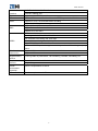
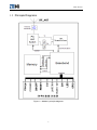
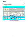
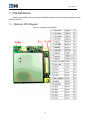
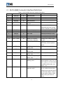
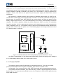
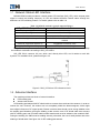
GSM Modules ZTE MG2636 Module Hardware Design User Manual Version: V1.0 This user manual is for MG2636 module GSM Modules Copyright Statement Copyright © 2010 by ZTE Corporation All rights reserved. No part of this publication may be excerpted, reproduced, translated or utilized in any form or by any means, electronic or mechanical, including photocopying and microfilm, without the prior written permission of ZTE Corporation. is the registered trademark of ZTE Corporation. All other trademarks appeared in this manual are owned by the relevant companies. ZTE Corporation reserves the right to make modifications on print errors or update specifications in this manual without prior notice. ZTE Corporation keeps the right to make the final explanation to this manual. 1.0-TY edition in Apr. 2010 1 GSM Modules With strong technical force, ZTE Corporation can provide CDMA/GPRS module customers with the following all-around technical support: 1. Provide complete technical documentation; 2. Provide the development board used for R&D, test, production, after-sales, etc.; 3. Provide evaluations and technical diagnosis for principle diagram, PCB, test scenarios; 4. Provide test environment; ZTE Corporation provides customers with onsite supports, and also you could get supports through telephone, website, instant communication, E-mail, etc. The module website module.ztemt.com.cn provides the relevant industry information and module technical documentation. The authorized module customers could download the latest technical documentation for our website. If you have more requirements, you could send an E-mail to [email protected]. You can also call us at 0755-86140899 for more supports. 2 GSM Modules Preface Summary This user manual is for MG2636 modules. It takes MG2636 modules for example to give the reference to the relevant hardware and mechanical design. This manual could instruct the users how to quickly and conveniently design different kinds of wireless terminals based on this type of module. Target Readers System designing engineers Mechanical engineers Hardware engineers Software engineers Test engineers Brief Introduction This manual contains 4 chapters. See the table below: Chapter Contents 1. General Description Introduces MG2636 module’s basic functions, principle diagrams, application diagrams, the relevant documents for reference. 2. PIN Definitions Introduces MG2636 module’s PIN name and functions. 3. Description of Hardware Interface Introduces the design of the hardware interface on each part of MG2636 modules. 4. Mechanical Design Introduces MG2636 module’s appearance diagram and assembly diagram. Update History The update history records the document’s update descriptions every time. The updates of all previous versions will be contained in the latest version. Document Version V1.0 (2010-04-22) The document is formally released on Apr. 22, 2010. 3 GSM Modules Contents 1 2 General Description...................................................................................................................... 7 1.1 Functions ........................................................................................................................................7 1.2 Principle Diagrams .........................................................................................................................9 1.3 Application Diagrams ...................................................................................................................10 1.4 Relevant Documents ....................................................................................................................11 1.5 Acronyms......................................................................................................................................11 PIN Definitions............................................................................................................................ 14 2.1 Module’s PIN Diagram..................................................................................................................14 2.2 50-Pin B2B Connector Interface Definitions.................................................................................15 3 Decription of Hardware Interfaces .............................................................................................. 18 3.1 Summary ......................................................................................................................................18 3.2 Power and Reset ..........................................................................................................................18 3.2.1 Power ................................................................................................................................18 3.2.2 Power On/Off ....................................................................................................................19 3.2.3 Reset .................................................................................................................................20 3.3 COM Port......................................................................................................................................20 3.4 SIM Card Interface .......................................................................................................................21 3.5 Audio Interface .............................................................................................................................22 3.5.1 Microphone .......................................................................................................................23 3.5.2 Receiver ............................................................................................................................23 3.6 DAI (Digital Audio Interface) .........................................................................................................23 3.7 Network Status LED Interface ......................................................................................................24 3.8 Antenna Interface .........................................................................................................................24 4 Mechanical Design ..................................................................................................................... 26 4.1 Appearance Diagram ...................................................................................................................26 4.2 Assembly Diagrams .....................................................................................................................26 4.2.1 MG2636 Module’s Assembly Diagram Dimensions..........................................................27 4.2.2 B2B Connector Socket......................................................................................................27 4 GSM Modules Figure Contents Figure 1-1 Module’s principle diagrams................................................................................................9 Figure 1-2 Module’s application diagrams ..........................................................................................10 Figure 2.1 Module’s PIN Diagram.......................................................................................................14 5 GSM Modules Table Contents Table 1-1 Table of functions .................................................................................................................7 Table 1-2 Table of Acronyms .............................................................................................................11 Table 2-1 50-Pin B2B Connector Interface Definitions .......................................................................15 6 GSM Modules 1 General Description This user manual is for MG2636 modules. Refer to this manual to make your hardware and mechanical design fully compatible with GSM/GPRS applications, except for antenna design. With the function of voice, SMS and data service, ZTE MG2636 module can be used for data transmission, wireless POS, security and surveillance, lottery terminal, intelligent metering system, wireless fax, small switch, tobacco communication system, campus communications, wireless AD, wireless media, medical surveillance, direct discharge station surveillance, railway terminals, intelligent home appliances and vehicle-mounted monitoring, etc. This manual describes MG2636 module’s logic structure, hardware interface & major functions, and provides references to the hardware and mechanical design. 1.1 Functions Table 1-1 Table of functions Basic functions Descriptions Work frequency (Dual band: EGSM9000/ DCS1800) EGSM900 Max. Tx power EGSM900: Class4 (2W) 31~35dBm (typical value: 33 dBm) DCS1800: Class1 (1W) 28~32dBm (typical value: 30 dBm) Transmit (uplink: MS→BTS): 880~915 MHz Receive (downlink: BTS→MS): 925~960 MHz DCS1800 Transmit (uplink: MS→BTS) : 1710~1785 MHz Receive (downlink: BTS→MS): 1805~1880 MHz Rx. Sensitivity <-106 dBm Work temperature Normal work temperature: -20°C~+55°C Expanded work temperature: -30°C~+70°C Storage temperature: -40°C~+85°C Voltage 3.4V~4.7V (recommended value: 3.8V) Power consumption (current) Power off current: 50uA Standby average current: 2.5mA GPRS Class10 (MAX): 300mA UART0 interface (8-wire hardware flow control, max. data rate: 921600bps), support download and data communication Application interface (50Pin B2B connector) UART1 interface (4-wire hardware flow control, max. data rate: 921600bps) Standard SIM card interface (1.8V/3.0V), support R-UIM 2CH analog audio I/O interface, using differential signals 1CH serial digital audio interface, using PCM encoding analog audio signal to digital signal Power management interface (including power interface and charge interface) Network status indication interface (different network status indicated by LED’s different flashing modes ) Power on-off interface (externally power on/off the module through the interface (indirect switch power) ) Reset interface (externally reset the module through the interface) 7 GSM Modules Antenna interface MURATA: MM9329-2700RA1 50-ohm antenna connector Protocol Support GSM/GPRS Phase2/2+ AT command Refer to《AT Command Set User Manual of ZTE Corporation’s MG2636 modules》 Voice Support FR, EFR, HR and AMR audio encoding Antenna’s welding pad Support hands-free talk, echo suppression function Support MO and MT SMS Support Point to Point and cell broadcast Support TEXT and PDU GPRS CLASS 10 Encoding method: CS 1,CS 2,CS 3,CS 4 Max. downlink transmitting rate: 85.6 kbps GPRS Max. uplink transmitting rate: 42.8 kbps Support PBCCH and virtual online; Embedded TCP/IP protocol: support multi-link, provides ACK and large capacity cache; Circuit domain data service Support CSD data service, max. data rate: 14.4Kbit/s Supplementary service Incoming caller ID presentation, call forwarding, call held, call waiting, etc. Physical features Dimensions: 35±0.10 x 32.5±0.10 x 3.85±0.20 mm ROHS environment protection Meet the requirements of ROHS CE certification Meet the requirements of CE Support USSD Weight: 7.0 g 8 GSM Modules 1.2 Principle Diagrams Figure 1-1 Module’s principle diagrams 9 GSM Modules 1.3 Application Diagrams Figure 1-2 Module’s application diagrams 10 GSM Modules 1.4 Relevant Documents 《AT Command Manual for ZTE Corporation's MG2636 Modules》 《ZTE Corporation GPRS modules FAQ》 《Wireless modules’ Test References》 1.5 Acronyms Table 1-2 Table of Acronyms A ADC Analog-Digital Converter 模数转换 AFC Automatic Frequency Control 自动频率控制 AGC Automatic Gain Control 自动增益控制 ARFCN Absolute Radio Frequency Channel Number 绝对射频信道号 ARP Antenna Reference Point 天线参考点 ASIC Application Specific Integrated Circuit 专用集成电路 BER Bit Error Rate 比特误码率 BTS Base Transceiver Station 基站收发信台 CDMA Code Division Multiple Access 码分多址 CDG CDMA Development Group CDMA 发展组织 CS Coding Scheme 译码图案 CSD Circuit Switched Data 电路交换数据 CPU Central Processing Unit 中央处理单元 DAI Digital Audio interface 数字音频接口 DAC Digital-to-Analog Converter 数模转换 DCE Data Communication Equipment 数据通讯设备 DSP Digital Signal Processor 数字信号处理 DTE Data Terminal Equipment 数据终端设备 DTMF Dual Tone Multi-Frequency 双音多频 DTR Data Terminal Ready 数据终端准备好 EDGE Enhanced Data Rate for GSM Evolution 提高数据速率的 GSM 演进技术 EFR Enhanced Full Rate 增强型全速率 EGSM Enhanced GSM 增强型 GSM B C D E 11 GSM Modules EMC Electromagnetic Compatibility 电磁兼容 EMI Electro Magnetic Interference 电磁干扰 ESD Electronic Static Discharge 静电放电 ETS European Telecommunication Standard 欧洲通信标准 FDMA Frequency Division Multiple Access 频分多址 FR Full Rate 全速率 GPRS General Packet Radio Service 通用分组无线业务 GSM Global Standard for Mobile Communications 全球移动通讯系统 Half Rate 半速率 IC Integrated Circuit 集成电路 IMEI International Mobile Equipment Identity 国际移动设备标识 ISO International Standards Organization 国际标准化组织 ITU International Telecommunications Union 国际电信联盟 LCD Liquid Crystal Display 液晶显示器 LED Light Emitting Diode 发光二极管 MCU Machine Control Unit 机器控制单元 MMI Man Machine Interface 人机交互接口/人机界面 MS Mobile Station 移动台 MTBF Mean Time Before Failure 平均故障间隔时间 PCB Printed Circuit Board 印刷电路板 PCL Power Control Level 功率控制等级 PCS Personal Communication System 个人通讯系统 PDU Protocol Data Unit 协议数据单元 PLL Phase Locked Loop 锁相环 PPP Point-to-point protocol 点到点协议 RAM Random Access Memory 随机访问存储器 RF Radio Frequency 无线频率 F G H HR I L M P R 12 GSM Modules ROM Read-only Memory 只读存储器 RMS Root Mean Square 均方根 RTC Real Time Clock 实时时钟 SIM Subscriber Identification Module 用户识别卡 SMS Short Message Service 短消息服务 SMT Surface Mount Technology 表面安装技术 SRAM Static Random Access Memory 静态随机访问存储器 TA Terminal adapter 终端适配器 TDMA Time Division Multiple Access 时分多址 TE Terminal Equipment also referred it as DTE 终端设备,也指 DTE UART Universal asynchronous receiver-transmitter 通用异步接收/发送器 UIM User Identifier Management 用户身份管理 USB Universal Serial Bus 通用串行总线 USIM Universal Subscriber Identity Module 用户识别模块 Voltage Standing Wave Ratio 电压驻波比 ZTE Corporation 中兴通讯股份有限公司 S T U V VSWR Z ZTE 13 GSM Modules 2 PIN Definitions Adopting 50-Pin B2B connector interface, MG2636 module has 50 pins with the distance 0.5mm between the pins. 2.1 Module’s PIN Diagram Figure 2.1 Module’s PIN Diagram 14 GSM Modules 2.2 50-Pin B2B Connector Interface Definitions Table 2-1 50-Pin B2B Connector Interface Definitions Functions PIN No. Definitions I/O Descriptions 1 SIM-CLK O SIM card clock 2 SIM-VCC O SIM card power 3 SIM-DATA I/O SIM card data 4 SIM-RST O SIM card reset 5 ISENSE AI Current inductor detect current 6 SIM-GND P SIM card GND SIM card’s GND PIN and SIM-GND PIN must connect with the module’s power GND. 7 DAIRXD I DAI: receive data internal pull-down(51.1KΩ) 8 DAISYNC O DAI: frame SYNC 9 DAICLK O DAI: clock 10 DAITXD O DAI: transmit data 11 DAIRST O DAI: reset internal pull-down(51.1KΩ) 12 BATT_TEMP AI Battery ID or battery temperature detection Analog input voltage range: 0~2.8V 13 SIG_LED O Network signal LED High level LED ON, need externally connect dynatron driver 14 RXD1 O UART1 corresponding to DTE’s RXD internal pull-down(75KΩ) 15 RXD0 O UART0 corresponding to DTE’s RXD internal pull-down(75KΩ) 16 TXD1 I UART1 corresponding to DTE’s TXD internal pull-down(75KΩ) 17 TXD0 I UART0 corresponding to DTE’s TXD internal pull-down(75KΩ) 18 BAT_BACKUP P Real-time clock (RTC) backup power Connect button battery or large capacitor. Input: 2.2~5V; max. output: 2.6~2.85V;under POWER DOWN mode, min. input: 1.3V. 19 CHRIN P External charge power detection input 4.2V~8V (recommended 5.5V), external connect the charge power with the current no less than 800mA. This pin is just used as diction. And It will be hung out when not used. 15 Max. output current 20mA internal pull-down(51.1KΩ) GSM Modules 20 GATEDRV O Battery charge control switch 21 GND P GND 22 GND P 23 GND P 24 GND P 25 GND P 26 BATT+ P 27 BATT+ P 28 BATT+ P 29 BATT+ P 30 BATT+ P 31 VDDIO 32 Valid at low level Work current anode input 3.4V~4.7V (recommended 3.8V), as the module transmits with the max. power, the current will instantly reach 1.6A. The min, value of BATT+ voltage is no lower than 3.3V, and the current no lower than 2A. O Module output digital interface voltage Typical value: 2.85V(MIN: 2.75V,MAX: 2.95V,MAX current: 150mA). There is voltage output only as the module is powered on. And It will be hung out when not used. RING0 O UART0 corresponding to DTE’s RING internal pull-down(75KΩ) 33 DSR0 O UART0 corresponding to DTE’s DSR internal pull-down(75KΩ) 34 RTS0 I UART0 corresponding to DTE’s RTS internal pull-down(75KΩ) 35 DTR0 I UART0 corresponding to DTE’s DTR internal pull-down(75KΩ) 36 RTS1 I UART1 corresponding to DTE’s RTS internal pull-down(75KΩ) 37 CTS0 O UART0 corresponding to DTE’s CTS internal pull-down(75KΩ) 38 CTS1 O UART1 corresponding to DTE’s CTS internal pull-down(75KΩ) 39 DCD0 O UART0 corresponding to DTE’s DCD internal pull-down(75KΩ) 40 SYSRST_N I Module’s reset Valid at low level, need externally connect dynatron driver. It’s recommended to parallel connect 0.1uF capacitor to GDN for ESD protection near 50-pin B2B connector. 16 GSM Modules 41 PWRKEY_N I Module’s power on/off 42 AGND P GND 43 MIC1_N AI 1CH audio input cathode 44 MIC1_P AI 1CH audio input anode 45 MIC2_P AI 2CH audio input anode 46 MIC2_N AI 47 SPK1_N AO 1CH audio output cathode 48 SPK1_P AO 1CH audio output anode 49 SPK2_P AO 2CH audio output anode(right ear) 50 SPK2_N AO 2CH audio output cathode(left ear) Valid at low level, need externally connect dynatron driver. Default audio I/O is the first channel. Usually the first channel is used for the receiver and the second channel used for headset or hands-free. 2CH audio input cathode Note: 1) I-representing digital signal input PIN; O-representing digital signal output PIN; AI - representing analog signal input PIN; AO - representing analog signal input PIN; ; P - representing power PIN; 2)UART0 and UART1 are named by DCE PIN signals. 17 GSM Modules 3 Decription of Hardware Interfaces 3.1 Summary This chapter introduces MG2636 module’s each function & its operation descriptions, and provides the designing sample. Power interface Charge interface Power on/off interface Reset interface UART interface (2CH) SIM Card Audio Interface (2CH analog audio interface) DAI interface (1CH digital audio interface) Network signal indication interface Antenna interface Other 3.2 Power and Reset 3.2.1 Power MG2636 GSM module requires VBAT and real-time clock BAT_BACKUP to work normally. For details, please see the following table 3-1 Power PIN Interface Definitions. Table 3-1 Power PIN Interface Definitions PIN No. Signal Name I/O Descriptions of Functions Remarks 21~25 GND P GND 26~30 BATT+ P Work Power Anode Input 3.4V~4.7V (recommended 3.8V), as the module transmits with the max. power, the current will instantly reach 1.6A. The min, value of BATT+ voltage is no lower than 3.3V, and the current no lower than 2A. 18 BAT_BACKUP P Real-time Clock (RTC) Backup Connect button battery or large capacitor. Input: 2.2~5V; max. output: 2.6~2.85V;under POWER DOWN mode, min. input: 1.3V. MG2636 module requires external power supply and the power supply voltage ranges from 3.4V~4.7V (typical value 3.8V). The external power supplies the power to the module through B2B connector’s VBAT PIN. As the module transmits with the max. power, the current will instantly reach 18 GSM Modules about 1.6A and VBAT voltage will fall down, however the min, value of BATT+ voltage must be no lower than 3.4V. The external power can provide the current required at MAX. Tx. Power, and it’s recommended to use LDO or switch power with the output current larger than 2A and a 100uF energy storage capacitor is parallel connected at the power end of the module. In order to guarantee the supply of current, use 5PIN on the power loop as the power supply and GND return current respectively. BAT_BACKUP is real-time backup input interface of MG2636 GSM module. As VBAT is ON, real-time clock could supply power through VBAT; as VBAT is not ON, BAT_BACKUP will supply the backup power for real-time clock. BAT_BACKUP can use the battery to supply the power and the battery voltage ranges from 2.8~5V. If the backup battery is not used, it could externally connect the capacitor. The value of capacitor decides the clock’s duration as VBAT is not ON. The calculation formula is as below: t=C/15; t represents the real-time clock’s duration (unit: s), and C represents the value of capacitor (unit: uF). The required current is about 15uA as MG2636 modules maintains the real-time clock function upon the power cut-off. The following figure is the charge reference circuit of RTC backup battery or capacitor. Figure 3-1 MG2636 Module’s RTC Backup Battery/Capacitor Reference Circuit AS VBAT> backup battery, it can charge the backup battery, and the charging cut-off voltage is 3.3V; as the battery does not work, RTC work current is 15uA. 3.2.2 Power On/Off The module is under power-off status after it’s normally powered on. To turn on the module, provide a 2000-3000mS low level pulse to PWRKEY_N pin when the module is OFF. In Data mode, if you connect VCHG to VPH_PWR, the module will be automatically powered on. It’s specially noted that PWRKEY_N is valid at low level, which is required externally to connect dynatron driver. It’s recommended to parallel connect 0.1uF capacitor to GDN for ESD protection near 50-pin B2B connector 19 GSM Modules 3.2.3 Reset SYSRST_N PIN is used to reset the module’s main chip, and SYSRST_N signal needs to be pulled down 200ms to reset the module. Likewise, this pin is required externally to connect dynatron driver and parallel connect 0.1uF capacitor to GDN to prevent SYSRST_N signal from external interference. And it’s noted that the wiring of 50pin connector must be as short as possible. 3.3 COM Port The module provides 1CH serial interface, supports 8-wire serial BUS interface or 4-wire serial BUS interface or 2-wire serial interface. The module communicates with the external devices and inputs AT commands through UART interface. UART supports programmable data width, programmable data stop bit, programmable parity check or no check, and UART port supports from 300bit/s to 921.6kbit/s baud rate. The default baud rate is 115200bit/s and it supports baud rate storage upon power drop. MG2636 module can directly connect the same signal name of DTE devices. Please see table 3-2 module UART signal names and figure 3-2 for the connection diagram between the module and DTE device. Table 3-2 MG2636 module UART external device’s signal names and functions PIN No. Signal Name I/O Descriptions of Functions Remarks 32 RING0 O UART0 port, corresponding to DTE’s RING port Internal pull-up(75KΩ) 33 DSR0 O UART0 port, corresponding to DTE’s DSR port Internal pull-up(75KΩ) 34 RTS0 I UART0 port, corresponding to DTE’s RTS port Internal pull-up(75KΩ) 35 DTR0 I UART0 port, corresponding to DTE’s DTR port Internal pull-up(75KΩ) 36 RTS1 I UART1 port, corresponding to DTE’s RTS port Internal pull-up(75KΩ) 37 CTS0 O UART0 port, corresponding to DTE’s CTS port Internal pull-up 75KΩ) 38 CTS1 O UART1 port, corresponding to DTE’s CTS port Internal pull-up(75KΩ) 39 DCD0 O UART0 port, corresponding to DTE’s DCD port Internal pull-up(75KΩ) 20 GSM Modules Figure 3-2 MG2636 module external DTE device’s circuit connection diagram MG2636 module can communicate with RXD and TXD of single chip microcomputer to compose the simplest 2-line mode. It’s noted that MG2636 module’s PIN level typical value is 2.8V, and interface level range 2.4V~3.1V. Likewise, the module can also communicate with the standard RS232 device. Due to the different interface level, 232 chip must be added for level conversion, e.g., use MAX3232 for 2-wire serial port and use MAX3238 for 8-wire serial port. The connection is the same as DTE device above. 3.4 SIM Card Interface The module supports 1.8V/3V UIM card, and there are 4 pins at the terminal of the card. VREG_RUIM is used to supply the UIM card. It’s strongly recommended to add ESD to protect the UIM card in hostile environments. FV2 in figure 4-4 is ESD protection device: MG2636 module baseband processor integrates SIM card interface conforming to ISO 7816-3 standard, and it’s compatible with SIM card with two voltages 1.8V/3.0V and reserves SIM card interface signal on B2B connector. Users should note that SIM card’s electrical interface definitions are the same as SIM card socket’s definitions. See table 3-3 for MG2636 module’s B2B connector’s interface definitions. Table 3-3 MG2636 module’s SIM card signal PIN No. Signal Name I/O Descriptions of Functions 1 SIM-CLK O SIM card clock 2 SIM-VCC O SIM card power 3 SIM-DATA I/O SIM card data 4 SIM-RST O SIM card reset 6 SIM-GND P SIM card GND 21 Remarks Max. output current 20mA SIM card’s GND PIN and SIM-GND PIN must connect with the GSM Modules module’s power GND. Figure 3-3 Standard SIM card PIN Definitions As shown in figure 3-4, the module connects the external SIM card and SIM-VPP could directly connect SIM-VCC. 33 ohm resistor on 3 wires has been parallel connected with the capacitor to guarantee the compatibility of SIM card with different electrical performances; meantime it can also meet the requirements of EMC test standards. Figure 3-4 Connection Diagram of MG2636 module and external SIM card Besides, since SIM card design should meet the requirements of ESD electrical performances to avoid the damage of SIM card, it’s recommended to add TVS component on 4-CH SIM card signal, meantime, the signal wire need first pass TVS component and enter the module’s baseband processor to avoid the damage of module. 3.5 Audio Interface MG2636 GSM module supports 2CH audio signal input/output. When it’s used for hand held devices, the hand held MIC, hand held receiver or hands-free speaker, headset MIC, headset receiver could be divided. See table 3-4 for the audio interface signals. Table 3-4 MG2326 module’s audio input signals PIN No. Signal Name I/O Descriptions of Functions Remarks 43 MIC1_N AI 1CH audio input cathode 44 MIC1_P AI 1CH audio input anode 45 MIC2_P AI 2CH audio input anode 46 MIC2_N AI 2CH audio input cathode 47 SPK1_N AO 1CH audio output cathode 48 SPK1_P AO 1CH audio output anode !st channel is the default audio input/output. Usually 1st channel used for receiver, 2nd channel used for 22 GSM Modules 49 SPK2_P AO 2CH audio output anode (right ear) 50 SPK2_N AO 2CH audio output anode(left ear) headset hands-free. or 3.5.1 Microphone The two microphone interfaces MIC1 and MIC2 are both differential interfaces, which could also be used for single-end input. It’s recommended to use differential mode and meet the requirements of differential signals during the wiring layout and the wiring must be as short as possible to reduce the noises. These two inputs are coupled in AC domain and added a 1.8V offset voltage inside, and they should directly connect with the microphone. ON the circuit design, add 33pF filter capacitor to the audio signal wire to reduce the interferences caused by the external antenna; meantime add TVS components accordingly. 3.5.2 Receiver The receiver interfaces are SPK_1 and SPK_2. SPK_1 is differential interface with 32Ω resistance; SPK_2 is the single-end interface with 32Ω resistance. Due to the differences between SPK_1 and SPK_2, SPK_1 is usually used as hand hold device’s Receiver, and SPK_2 is used for headset’s left/right ears. Note: Differential design of audio signals could suppress the noise, and the PCB wiring must be as short as possible. The differential signals must be kept far away from the power, RF and antenna circuit. 3.6 DAI (Digital Audio Interface) DAI digital audio interface adopts PCM encoding from analog signal to digital signal, which could connect with devices for digital audio communications, such as Bluetooth device, and it is convenient for users to develop peripheral audio communicating system. Table 3-5 MG2636 module DAI PIN No. Signal Name I/O Descriptions of Functions 7 DAIRXD I DAI: Rx data 8 DAISYNC O DAI: frame SYNC 9 DAICLK O DAI: clock 10 DAITXD O DAI: Tx data 11 DAIRST O DAI: reset 23 Remarks Internal pull-down (51.1KΩ) Internal pull-down (51.1KΩ) Internal pull-down (51.1KΩ) GSM Modules 3.7 Network Status LED Interface MG2636 GSM module provides a network status LED interface (SIG_LED), which outputs pulse signal to control the blinking frequency of LED and indicate different network status through the definitions of LED’s blinking modes. For details, please refer to table 3-6. Table 3-6 MG2636 module’s network status definitions SIG_LED PIN Output Status Work or Network Status Output high level Module startup Continue high level Module calling Continue low level Deep sleep Period 1s, high level output 0.1s No SIM card, not enter PIN or searching network Period 3s, high level output 0.1s Registered to network, IDLE Period 0.125s, high level output 0.1s GPRS data transmitting SIG_LED PIN output status is defined according to the software protocol, and users could judge the module’s work status according to SIG_LED status. SIG_LED PIN is common I/O port, which can’t directly drive LED, and it needs to work with dynatron. For detailed circuit, please see figure 3-5. Figure 3-5 SIG_LED driver LED reference circuit 3.8 Antenna Interface The module provides two kinds of antenna interface: PCB welding pad Antenna test socket PCB welding pad adopts 50Ω RF shield cable to connect the module and the antenna, in order to reduce the cost. However, this method can not completely shield the electromagnets, which might have slight influence on RF signal quality. Please note that there should not be strong radiation near the welding pad. Meantime, during the welding, make sure the core of RF shield cable must connect with RF welding pad, and RF shield cable’s shield metal mask must be welded to the module’s GND. During the welding, the GND must be welding securely, otherwise, the core is easily broken due to the shaking of shield cable. See figure 3-6 for RF welding pad antenna. 24 GSM Modules Figure 3-6 MG2636 module RF welding pad antenna The antenna test socket is used for the module’s calibration and test. The contact resistance is small and the shielding is good. An exclusive 50Ω socket to SMA connection cable is used to connect the module and the antenna. The antenna test socket’s resistance is 50Ω. The antenna test socket’s part number is MM9329-2700B. Please refer the socket manufacturer’s manual to select the relevant antenna to connect the plug and module. Figure 3-7 MG2636 module’s RF test socket 25 GSM Modules 4 Mechanical Design 4.1 Appearance Diagram MG2636 module’s appearance Figure 3-8 MG2636 module’s appearance Dimensions(LxWxH) : 35±0.10 x 32.5±0.10 x 3.85±0.20 mm Weight: 7g 4.2 Assembly Diagrams 26 GSM Modules 4.2.1 MG2636 Module’s Assembly Diagram Dimensions Figure 4-2 MG2636 Module’s Assembly Diagram Technical requirements: 1)*Dimensions. Representing check the dimensions; 2)tolerances +-0.1mm。 4.2.2 B2B Connector Socket In order to meet the requirements of electrical performances of B2B connector, users should select the proper connector. The part number of the connector for MG2636 module is DF12C(3.0)-50DS-0.5V(81). Users can refer to DF12C(3.0)-50DS-0.5V(81) specifications to search for the matched connector. Remarks: DF12C (3.0)-50DS-0.5V (81) is Shenzhen JieRong Technology Co., Ltd. 27 GSM Modules Figure 4-3 MG2636 module connector’s assembly status Figure 4-4 MG2636 module connector’s relevant appearance diagram 28