1
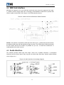
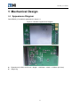
ME3000_V2 Module ZTE Corporation’s ME3000_V2 Module Hardware Design User Manual Version: V1.0 This manual is applicable for ME3000_V2 module. ME3000_V2 Module Copyright Statement Copyright © 2010 by ZTE Corporation All rights reserved. No part of this publication may be excerpted, reproduced, translated or utilized in any form or by any means, electronic or mechanical, including photocopying and microfilm, without the prior written permission of ZTE Corporation. is the registered trademark of ZTE Corporation. All other trademarks appeared in this manual are owned by the relevant companies. ZTE Corporation reserves the right to make modifications on print errors or update specifications in this manual without prior notice. ZTE Corporation keeps the right to make the final explanation to this manual. 1.0-TY, March 2010 1 ME3000_V2 Module With strong technical force, ZTE Corporation can provide CDMA/GPRS module customers with the following all-around technical support: 1. Provide complete technical documentation; 2. Provide the development board used for R&D, test, production, after-sales, etc.; 3. Provide evaluations and technical diagnosis for principle diagram, PCB, test scenarios; 4. Provide test environment; ZTE Corporation provides customers with onsite supports, and also you could get supports through telephone, website, instant communication, E-mail, etc. The module website module.ztemt.com.cn provides the relevant industry information and module technical documentation. The authorized module customers could download the latest technical documentation for our website. If you have more requirements, you could send an E-mail to [email protected]. You can also call us at 0755-86140899 for more supports. 2 ME3000_V2 Module Preface Summary This manual is applicable for ME3000_V2 module. It takes ME3000_V2 module for example to give the reference to the relevant hardware design and instruct the users how to quickly and conveniently design different kinds of wireless terminals based on this type of module. ME3000_V2 modules are the replacement of ME3000 modules and their technical parameters are basically identical. Target Readers The manual is suitable for the following engineers: System designing engineers Mechanical engineers Hardware engineers Software engineers Test engineers Brief Introduction This manual contains 6 chapters. See the table below: Chapter Contents 1 General description Introduces ME3000_V2 module’s basic technical specification, the relevant documents for reference and the acronyms. 2 Product introduction Introduces ME3000_V2 module’s principle charts and relevant standards of the module. 3 PIN definitions Introduces ME3000_V2 module’s Pin name and functions. 4 Description hardware interfaces of Introduces the design of the hardware interface on each part of ME3000_V2 module. 5 Mechanical design Introduces ME3000_V2 module’s appearance diagram, assembly diagram, PCB layout diagram and fixing method. 6 Summary of peripheral components Introduces the peripheral components. Update History The update history records the document’s update descriptions every time. The updates of all previous versions will be contained in the latest version. Document Version V1.0 (2010-03-15) The document is formally released on Mar. 15, 2010. 3 ME3000_V2 Module Contents 1 2 3 4 5 6 General Description...................................................................................................................... 7 1.1 Technical Specification .......................................................................................................... 7 1.1.1 Module’s Specification ................................................................................................ 7 1.1.2 Basic Functions .......................................................................................................... 7 1.1.3 Module’s Interface ...................................................................................................... 7 1.1.4 Technical parameters ................................................................................................. 8 1.2 Relevant Documents ............................................................................................................. 8 1.3 Acronyms .............................................................................................................................. 9 Product Introduction ................................................................................................................... 12 PIN Definitions............................................................................................................................ 13 3.1 40PIN Connector................................................................................................................. 13 3.2 10PIN Connector................................................................................................................. 16 Decription of Hardware Interfaces .............................................................................................. 17 4.1 Summary............................................................................................................................. 17 4.2 Power and Reset................................................................................................................. 17 4.3 COM Port ............................................................................................................................ 19 4.4 SIM Card Interface .............................................................................................................. 20 4.5 Audio Interface .................................................................................................................... 20 4.6 Antenna Interface................................................................................................................ 21 Mechanical Design ..................................................................................................................... 23 5.1 Appearance Diagram .......................................................................................................... 23 5.2 Assembly Diagram .............................................................................................................. 24 5.3 PCB Layout Diagram .......................................................................................................... 25 5.4 Fixing Method...................................................................................................................... 26 Summary of Peripheral Components ......................................................................................... 27 4 ME3000_V2 Module Diagrams Figure 2-1 Principle diagram………………………….…………………………………………………. 12 Figure 4-1 Power and reset circuit design principle diagram………………………………………… 17 Figure 5-1 Module’s Appearance Diagram…………………………………………………………….. 23 Figure 5-2 Module’s Assembly Diagram……………………………………………………………….. 24 Figure 5-3 Relevant PCB Layout Diagram (top side)…………………………………………………. 25 Figure 5-4 Module’s Fixing Methods……………………………………………………………………. 26 5 ME3000_V2 Module Tables Table 1-1 Table 1-1 Module’s specification……………………………………………………………… 7 Table 1-2 Basic functions …………………………………………………………………………………..7 Table 1-3 Interfaces of the modules……………………………………………………………………… 7 Table 1-4 Technical parameters ………………………………………………………………….………..8 Figure 3-1 PIN definitions………………………………………………………………….……………… 13 Table 3-1 40PIN connector definitions…………………………………………………………………... 13 Table 3-2 10PIN connector PIN definitions……………………………………………………………… 16 Table 4-1 Voltage features …………………………………………………………………………………17 Table 4-2 Power on/off ciruict time characteristics……………………………………………………… 18 Table 6-1 Summary of Peripheral Components…………………………………………………………. 27 6 ME3000_V2 Module 1 General Description This manual is applicable for ME3000_V2 modules. Refer to this manual to make your hardware, mechanical design completely compatible with GSM/GPRS applications except for antenna design. ME3000_V2 module could be widely applied in data transmission, wireless POS, security, lottery terminals, intelligent metering, wireless fax, branch exchange, tobacco network, campus network, wireless AD, wireless media, medical surveillance, relay station surveillance, railway terminals, intelligent home appliances, vehicle-mounted surveillance, etc. Taking ME3000_V2 module for example, this manual describes the module’s logic structure, hardware interface & major functions, and provides references to the hardware and mechanical design. 1.1 Technical Specification 1.1.1 Module’s Specification Please refer to table 1-1 for ME3000_V2 module’s specification. Table 1-1 Table 1-2 Module’s specification Models Format Frequency(MHz) MG3000_V2 GSM/GPRS Dual Band: EGSM 900/DCS 1800 Remarks: Except for work frequency band, the modules are completely compatible on hardware and mechanical design. Below is just an example of ME3000_V2 module. 1.1.2 Basic Functions Please refer to Table 1-3 for the basic functions. Table 1-3 Basic functions Basic Functions Descriptions Voice call EVRC and 13kQCELP high quality voice call SMS Support TEXT and PDU Data Support embedded TCP/IP Support virtual online GSM uplink rate 42.8 kbps, downlink rate 85.6 kbps. 1.1.3 Module’s Interface Please refer to Table 1-4 for the module’s interfaces. Table 1-4 Interfaces of the modules Module’s interfaces UART interface Descriptions Software download upgrade; Data communication; Up to 921.6kbps data rate provided by COM port; 7 ME3000_V2 Module Audio interface Double audio I/O channel. SIM card interface Standard SIM card interface Antenna interface 50 Ohm input resistance control RTC Real time clock interface 1.1.4 Technical parameters Please refer to Table 1-5 for the module’s technical parameters. Table 1-5 Technical parameters Technical parameters Descriptions Working temperature -20°C ~ +70°C Input voltage 3.3V-4.25V Maximum current 1800mA @ -102 dBm Idle current 10mA @ -75 dBm Call current 150mA @ -75 dBm Rx Sensitivity 102dBm Tx power GSM850, EGSM900:Class4(2W) GSM1800, PCS1900:Class1(1W) GSM850 Tx.: 824~849 MHz Rx.: 869~894MHz Frequency range EGSM900 Tx.: 880~915 MHz Rx.: 925~960MHz DCS1800 Tx.: 1710~1785MHz Rx.: 1805~1880MHz PCS1900 Tx.: 1850~1910MHz Rx.: 1930~1990MHz 1.2 Relevant Documents 《AT Command Manual for ZTE Corporation's ME3000_V2 Modules》 《ZTE MG815+ Module Development Board User Guide》 《FAQ for ZTE Corporation's GSM/GPRS Modules》 《Wireless Modules’ Test References》 8 ME3000_V2 Module 1.3 Acronyms A ADC Analog-Digital Converter AFC Automatic Frequency Control AGC Automatic Gain Control ARFCN Absolute Radio Frequency Channel Number ARP Antenna Reference Point ASIC Application Specific Integrated Circuit B BER Bit Error Rate BTS Base Transceiver Station C CDMA Code Division Multiple Access CDG CDMA Development Group CS Coding Scheme CSD Circuit Switched Data CPU Central Processing Unit D DAI Digital Audio interface DAC Digital-to-Analog Converter DCE Data Communication Equipment DSP Digital Signal Processor DTE Data Terminal Equipment DTMF Dual Tone Multi-Frequency DTR Data Terminal Ready E EDGE Enhanced Data Rate for GSM Evolution EFR Enhanced Full Rate EGSM Enhanced GSM EMC Electromagnetic Compatibility EMI Electro Magnetic Interference ESD Electronic Static Discharge ETS European Telecommunication Standard F FDMA Frequency Division Multiple Access FR Full Rate 9 ME3000_V2 Module G GPRS General Packet Radio Service GSM Global Standard for Mobile Communications H HR Half Rate I IC Integrated Circuit IMEI International Mobile Equipment Identity ISO International Standards Organization ITU International Telecommunications Union L LCD Liquid Crystal Display LED Light Emitting Diode M MCU Machine Control Unit MMI Man Machine Interface MS Mobile Station MTBF Mean Time Before Failure P PCB Printed Circuit Board PCL Power Control Level PCS Personal Communication System PDU Protocol Data Unit PLL Phase Locked Loop PPP Point-to-point protocol R RAM Random Access Memory RF Radio Frequency ROM Read-only Memory RMS Root Mean Square RTC Real Time Clock S SIM Subscriber Identification Module SMS Short Message Service SMT Surface Mount Technology SRAM Static Random Access Memory 10 ME3000_V2 Module T TA Terminal adapter TDMA Time Division Multiple Access TE Terminal Equipment also referred it as DTE U UART Universal asynchronous receiver-transmitter UIM User Identifier Management USB Universal Serial Bus USIM Universal Subscriber Identity Module V VSWR Voltage Standing Wave Ratio Z ZTE ZTE Corporation 11 ME3000_V2 Module 2 Product Introduction Please refer to Figure 2-1 for the principle diagram of ME3000_V2 module. Figure 2-1 Principle diagram 12 ME3000_V2 Module 3 PIN Definitions The main connectors used for ME3000_V2 module include 40-PIN connector and 10-PIN connector. The distance between the pins is 1.27mm. Refer to figure 3-1 below for PIN definitions. Figure 3-1 PIN definitions 3.1 40PIN Connector See the definitions of 40PIN conbector in table 3-1. Table 3-2 40PIN connector definitions Function Pin Signal name I/O Basic functions Remarks No. Audio COM 1 39 MIC_1P I 1st audio input anode 37 34 MIC_1N SPK_1P I O 1st audio input cathode 1st audio output anode 32 SPK_1N O 1st audio output cathode 40 MIC_2P I 2nd audio input anode 38 MIC_2N I 33 SPK_2P O 2nd audio output cathode 2nd audio output anode 35 EAR_AN_D ET I Earpiece key detection Internal pull-up, valid at low level 36 EAR_DET I Earpiece detection Internal pull-up, valid at low level 12 /CTS O Clear to send Valid at low level 14 /RTS I Request to send Valid at low level 13 TXD O Transmit data 11 RXD I Receive data 13 insert Default audio input/output as 1st channel. Usually 1st used for handset, 2nd userd for earpiece. ME3000_V2 Module Function SIM card interface COM 2 LED Reset Pin No. Signal name I/O Basic functions Remarks 15 RI—GPIO42 /EINT2 O Ringer indication signal TTL level. High level when initialized: Low level after receiving ringer signal and the incoming call rings; high level at any other time. No level change upon the receipt of SMS; 1s low level and 4s high level as the incoming call rings; the process repeats; high level at any other time. Generate 1s low level upon the receipt of SMS. 17 /DSR O Data Set Ready Valid at low level 18 DCD O Data Carrier Detect 16 /DTR I Data Terminal Ready 4 CARD_DAT A I/O Data cable 6 CARD_CLK O Clock cable 8 V_CARD O CARD power supply 2 CARD_RST O Reset signal 1 TXD2 O Transmit data 3 RXD2 I Receive data 5 /RTS2 I Request to send 7 /CTS2 O Clear to send The GSM module does not support USB function, but it supports UART2 only. Low level valid for PIN 5 and PIN 7. 9 GPIO17 GPIO Hang up when reserved 28 SMS_LED— —GPIO25 O Incoming call and SMS LED Internal pull-down, LED on at high level. Need externally add the driver. 4-5S low level upon the receipt of SMS. 30 SIG_LED O Network signal LED Internal pull-up, LED on at high level. Need externally add the driver. -Power on status: LED off. -Network status: LED flashes. LED is on for 50ms, and off for uncertain time. -IDLE status: LED flashes at 1Hz. -Traffic status (Call, network): LED flashes at 5Hz. 26 ON/OFF I Power on/off control Internal pull-up, valid at low level. Externally connect with a - 14 Valid at low level ME3000_V2 Module Function Pin No. Signal name I/O Basic functions Remarks switch with Open Collector (Open Drain). Please refer to 4.2 power and reset for details. Power 10 /RESET I Reset signal 19 V_MAIN I Main power supply 21 V_MAIN I Main power supply 22 V_MAIN I Main power supply GND GN D GND GN D 25 V_MSM O 20 NC - 27 NC - For module’s internal use, need hang up. 29 NC - For module’s internal use, need hang up. 31 NC - For module’s internal use, need hang up. 23 24 Reserved Digital power Valid at low level. Need externally connect a switch with Open Collector(Open Drain). Please refer to 4.2 power and reset for details. Generally, it’s recommended to use this pin for pull-up. As the module is powered off, the output voltage of the pin remains unchanged, but the internal resistance is very high. Therefore, it’s not recommended to use this pin for any other control purpose. For module’s internal use, need hang up. 15 ME3000_V2 Module 3.2 10PIN Connector See 10PIN connector definitions in table 3-2. Table 3-3 10PIN connector PIN definitions Function Pin No. Signal name I/O Basic functions 1 GND GND 2 GND GND 3 GND GND 4 GND GND 5 NC 6 NC 7 NC 8 NC 9 NC 0 NC Power Reserved For module’s need hang up. 16 internal use, ME3000_V2 Module 4 Decription of Hardware Interfaces 4.1 Summary This chapter introduces each logic function interfaces of ME3000_V2 module & its operation descriptions, and provides the designing sample. Power and Reset Interface COM Port SIM Card Interface Audio Interface Antenna Interface Remarks: In the system, the module layout should be far away from high-speed circuit, switch power, power transformer, large power inductor, or single chip microcomputer’s clock circuit. 4.2 Power and Reset See the power and reset circuit design principle diagram in figure 4-1. Figure 4-1 Power and reset circuit design principle diagram Power design The module is powered by V-MAIN. See the voltage features in figure 4-1. Table 4-1 Voltage features Category Min. Typical Max. Input voltage 3.3 V 3.9 V 4.25 V Inpput current 10mA (average) --- 2A (depending on network signal) D1 is an enabled LDO with 6V~9V input voltage. Through adjusting R31and R41, it could make V_MAIN at 3.9V to power ME3000_V2 module, and it’s required to place at lease one 1000uF tantalum capacitor at V-Main input pin. The module is very strict with the requirements on power and GND, therefore it’s requested that filtering must be performed to power and GND, and the power 17 ME3000_V2 Module ripple must be controlled under 50Mv. Do not use LDO to power any other part in the system because it might affect the RF performance. Finally, select the power cables with at least 80mil traces during the layout and keep the integrality of ground line. If you use other LDO, make sure the output current is larger than 2A. Power ON The module will be turned off after power-on normally. To turn on the module, provide a 2000-5000mS low level pulse to ON/OFF PIN. If connecting to GND at ON/OFF pin with 1K resistance, the module could be automatically powered on. Note: ON/OFF, /Reset need to connect an open collector or open drain gate. The /RESET signal is not required when the module is turned on. Power OFF To turn off the module, provide a 2000-5000mS low level pulse to ON/OFF PIN or use AT command “AT+ZPWROFF”. Reset The module could be reset by using the method above to “Turn off” and then “Turn on”. If the external reset function has to be used, one low level pulse lasting at least 500mS should be provided to /RESET Pin within 2 seconds after the module is turned on. Before that, the external I/O signal must be kept at low level. Refer to figure 4-2 Reset circuit design reference. If the /RESET Pin is not used, hang it up. See the module’s power-on/off time sequence diagram. Figure 4-2 Power-on/off time sequence diagram Table 4-2 Power on/off ciruict time characteristics ta tb tc td te 20mS 10mS 3S 3S 6S V_MSM There is a voltage output pin with current adjuster, which can be used to supply external power to the board. The voltage of this pin and the voltage of baseband processor/memory come from the same voltage adjuster. The voltage output is available only when the module is on. The normal output voltage is 2.85V, and the user should absorb the current from this pin as little as possible (less than 18 ME3000_V2 Module 10mA). Generally, it is recommended to use this pin to match the level. When the module is off, the output voltage for this pin remains unchanged, but the impedance is rather high. Therefore, it’s not recommended to use this pin for any other control purposes. Other Advice In order to make sure the data is saved safely, please don’t cut off the power when the module is on. It’s strongly recommended to add battery or soft switch like the power key on the mobile phone. 4.3 COM Port The module provides an integrated full duplex UART interface and an accessorial full duplex UART interface, whose maximal data rate is 115200bps. External interface is 2.85VCMOS level signal, their logic functions conform to RS-232 interface standard. These two UART could be used as serial port data interfaces, usually UART1 is used for AT commands, data transmission and updating software of module, UART2 is used to provide test and debug channel. Note: during the overall unit’s design, the customers need lead out UART1 for software upgrade. The module’s output IO level is 2.85VTTL, and it needs to transfer the level when connect with standard 3.3V or 5V logic circuit(such as MCU or RS232 drive chip MAX3238 etc), Figure 4-2 shows the COM port level transfer circuit. The converted signal should connect with MCU or RS232 drive chip directly. Common low power switch triode should be applied as the crystal triode shown in Figure 4-2. Note: the module won’t enter the sleep mode when RxD is at high level. Please pay attention to it during the design. Figure 4-2 UART Interface Design Diagram Note: The GSM module supports UART2 (note: including RTS2 and CTS2), but it does not support USB. 19 ME3000_V2 Module 4.4 SIM Card Interface ME3000_V2 supports 1.8V or 3V SIM card, and there are 4 pins at the terminal of the card. V_CARD is used to supply SIM card. It’s strongly recommended to add ESD to protect SIM card in hostile environments. D2 in figure 4-3 is ESD protection device: Figure 4-4 SIM Card Circuit Reference Design Diagram NOTE: A 10k resistor is required for DATA pin to be draw up to V_CARD power, because there are different SIM cards with quite different output currents. The PCB wiring of SIM card should be laid closely around the module as possible as you can, to avoid the interference of reading/writing from other sources. 4.5 Audio Interface The module provides audio input and output. There are 2 speaker interfaces, 2 microphone interfaces and one linear output. Only one pair I/O works at the same time. See the audio interface circuit in figure 4-4. Figure 4-5 Audio interface circuit design diagram 20 ME3000_V2 Module Microphone The system connector provides two microphone interfaces MIC_1 and MIC_2, which are both differential interface and can be used for single ended input. It’s recommended to use the differential mode to reduce the noises. These two microphone inputs are coupled in AC domain and added a 2.0V offset voltage inside, and they should directly connect with the receiver. Speaker The system connector provides two speakers, SPK_1 & SPK_2. The former is differential interface, and the latter is single-ended interface. They both have 32 ohm impedance. GSM/GPRS module audio interface is designed as below: Design of the first channel audio interface Select the microphone with the sensitivity lower than -51.5dB since the output impedance for SPK_1 is 32 ohm and the max. gain in MIC_1 reaches 51.5dB. The level of MIC_1P PIN is about 2.2V. Note: if other kind of audio input method is adopted, the input signal should be within 0.5V. If the signal voltage is lower than 0.5V, then the pre-amplifier should be added. If the signal voltage is higher than 0.5V, then network attenuation should be added. Design of the second channel audio interface on the earphone Select the microphone with the sensitivity lower than -51.5dB since the output impedance for SPK_2 is 32 ohm and the max. gain in MIC_2 reaches 51.5dB. The level of MIC_2P PIN is about 2.2V. The receiver’s design is just the same as the handset’s. 4.6 Antenna Interface The module provides two kinds of external interfaces: Directly solder with PCB land Antenna testing socket PCB land is used to connect module with antenna by 50 ohm RF shielding cable to cut down the cost. But it’s not a complete way to shield EMI, and RF signal quality may be trivially affected. So if you decide to use this method, intense radiation must keep far away from PCB land. At the same time, you must ensure that core line of RF shielding cable has been jointed to PCB land, and the shielding metal wire netting on the RF cable has been jointed to GND of module. As shown in figure 4-5, the grounding part must be jointed firmly, otherwise, the core cable may be ruptured caused by shielding cable shaking. Proper measures should be taken to reduce the access loss of effective bands, and good shielding should be established between external antenna and RF connector. Besides, external RF cables should be kept far away from all interference sources such as high-speed digital signal or switch power supply. 21 ME3000_V2 Module Figure 4-6 Antenna Interface Diagram The antenna test socket is used for the module’s calibration and test. It can easily connect the module to the antenna because of its small contact impedance, good shielding and exclusive 50Ω connection cable. The antenna test socket’s impedance is 50Ω. The antenna test socket’s part number is MM9329-2700B. Please refer to the user manual of socket’s supplier and select the relevant antenna connection plug to connect the module. See figure 4-6. Figure 4-7 Antenna Interface Diagram Proper measures should be taken to reduce the access loss of effective bands, and good shielding should be established between external antenna and RF connector. Besides, external RF cables should be kept far away from all interference sources such as high-speed digital signal or switch power supply. According to mobile station standard, stationary wave ratio of antenna should be between1.1 to 1.5, and input impedance is 50 ohm. Different environments may have different requirements on the antenna’s gain. Generally, the larger gain in the band and smaller outside the band, the better performance the antenna has. Isolation degree among ports must more than 30dB when multi-ports antenna is used. For example, between two different polarized ports on dual-polarized antenna, two different frequency ports on dual-frequency antenna, or among four ports on dual-polarized dual-frequency antenna, isolation degree should be more than 30dB. 22 ME3000_V2 Module 5 Mechanical Design 5.1 Appearance Diagram See ME3000_V2 module’s appearance in figure 5-1. Figure 5-1 Module’s Appearance Diagram Dimensions (LxWxH): 44.50 mm(length)x 28.50mm(width)x 8.25mm (±0.2mm) Weight: 8g 23 ME3000_V2 Module 5.2 Assembly Diagram See the module’s assembly diagram in figure 5-2. Figure 5-2 Module’s Assembly Diagram 24 ME3000_V2 Module 5.3 PCB Layout Diagram See the module’s PCB layout diagram in figure 5-3. Figure 5-3 Relevant PCB Layout Diagram (top side) 25 ME3000_V2 Module 5.4 Fixing Method The material of the metal plate used for the module’s fixing part is There are two fixing methods: welding or mounting screws. See the module’s fixing methods in figure 5-4. Figure 5-4 Module’s Fixing Methods 26 ME3000_V2 Module 6 Summary of Peripheral Components See the summary of peripheral components in table 6-1. Table 6-1 Summary of Peripheral Components Part Number Location No. Supplier Contact method MIC29302WU D1 MICREL www.micrel.com SPNZ-40S1-VB-030-1-R X1 Shenzhen Shentaiweixiang www.stwxe.com.cn PNY-10S2-VB-028(020) U1 Shenzhen Shentaiweixiang www.stwxe.com.cn C707 10M006 5122 U05 AMPHENOL www.amphenol.com VC060303A100RP ESD3-6 AVX www.avx.com 27