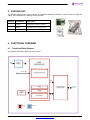
1
DS-MPE-GPIO
PCIe MiniCard Digital I/O Module with FPGA
Rev A.1 June 2015
Revision
Date
A.0
8/27/2014
A.1
6/17/15
FOR TECHNICAL SUPPORT
PLEASE CONTACT:
[email protected]
Comment
Initial release
Corrected pin out information
Copyright 2014
Diamond Systems Corporation
555 Ellis Street
Mountain View, CA 94043 USA
Tel 1-650-810-2500
Fax 1-650-810-2525
www.diamondsystems.com
CONTENTS
1.
2.
IMPORTANT SAFE HANDLING INFORMATION .............................................................................................3
INTRODUCTION ................................................................................................................................................4
2.1 Description .....................................................................................................................................................4
2.2 Features .........................................................................................................................................................4
2.3 Software Support ...........................................................................................................................................4
2.4 Mechanical, Electrical, Environmental ...........................................................................................................4
3. PACKING LIST...................................................................................................................................................5
4. FUNCTIONAL OVERVIEW ................................................................................................................................5
4.1 Functional Block Diagram ..............................................................................................................................5
4.2 Mechanical Board Drawing ............................................................................................................................6
5. INSTALLATION..................................................................................................................................................7
6. CONNECTOR PINOUT AND PIN DESCRIPTION ............................................................................................8
6.1 PCIe MiniCard Edge Connector ....................................................................................................................8
6.2 Digital I/O (J1, J2) ..........................................................................................................................................8
7. ARCHITECTURE OVERVIEW ...........................................................................................................................9
7.1 Bus Interface..................................................................................................................................................9
7.2 FPGA .............................................................................................................................................................9
7.3 Digital I/O .......................................................................................................................................................9
7.4 Pulse Width Modulators .................................................................................................................................9
7.5 Counter / Timers ............................................................................................................................................9
7.6 Protected Power ............................................................................................................................................9
7.7 Interrupt Circuit ..............................................................................................................................................9
8. SOFTWARE DRIVER OVERVIEW ................................................................................................................. 10
8.1 Configuring Using Universal Driver ............................................................................................................ 10
8.1.1
Interrupt level ..................................................................................................................................... 10
9. SPECIFICATIONS ........................................................................................................................................... 11
DS-MPE-GPIO User Manual Rev A.1
www.diamondsystems.com
Page 2
1. IMPORTANT SAFE HANDLING INFORMATION
WARNING!
ESD-Sensitive Electronic Equipment
Observe ESD-safe handling procedures when working with this product.
Always use this product in a properly grounded work area and wear appropriate
ESD-preventive clothing and/or accessories.
Always store this product in ESD-protective packaging when not in use.
Safe Handling Precautions
This board contains a high density connector with many connections to sensitive electronic components. This
creates many opportunities for accidental damage during handling, installation and connection to other
equipment. The list here describes common causes of failure found on boards returned to Diamond Systems for
repair. This information is provided as a source of advice to help you prevent damaging your Diamond (or any
vendor’s) embedded computer boards.
ESD damage – This type of damage is usually almost impossible to detect, because there is no visual sign of
failure or damage. The symptom is that the board eventually simply stops working, because some component
becomes defective. Usually the failure can be identified and the chip can be replaced. To prevent ESD damage,
always follow proper ESD-prevention practices when handling computer boards.
Damage during handling or storage – On some boards we have noticed physical damage from mishandling. A
common observation is that a screwdriver slipped while installing the board, causing a gouge in the PCB surface
and cutting signal traces or damaging components.
Another common observation is damaged board corners, indicating the board was dropped. This may or may not
cause damage to the circuitry, depending on what is near the corner. Most of our boards are designed with at
least 25 mils clearance between the board edge and any component pad, and ground / power planes are at least
20 mils from the edge to avoid possible shorting from this type of damage. However these design rules are not
sufficient to prevent damage in all situations.
A third cause of failure is when a metal screwdriver tip slips, or a screw drops onto the board while it is powered
on, causing a short between a power pin and a signal pin on a component. This can cause overvoltage / power
supply problems described below. To avoid this type of failure, only perform assembly operations when the
system is powered off.
Sometimes boards are stored in racks with slots that grip the edge of the board. This is a common practice for
board manufacturers. However our boards are generally very dense, and if the board has components very close
to the board edge, they can be damaged or even knocked off the board when the board tilts back in the rack.
Diamond recommends that all our boards be stored only in individual ESD-safe packaging. If multiple boards are
stored together, they should be contained in bins with dividers between boards. Do not pile boards on top of each
other or cram too many boards into a small location. This can cause damage to connector pins or fragile
components.
Power supply wired backwards – Our power supplies and boards are not designed to withstand a reverse
power supply connection. This will destroy each IC that is connected to the power supply (i.e. almost all ICs). In
this case the board will most likely will be unrepairable and must be replaced. A chip destroyed by reverse power
or by excessive power will often have a visible hole on the top or show some deformation on the top surface due
to vaporization inside the package. Check twice before applying power!
Overvoltage on digital I/O line – If a digital I/O signal is connected to a voltage above the maximum specified
voltage, the digital circuitry can be damaged. On most of our boards the acceptable range of voltages connected
to digital I/O signals is 0-5V, and they can withstand about 0.5V beyond that (-0.5 to 5.5V) before being damaged.
However logic signals at 12V and even 24V are common, and if one of these is connected to a 5V logic chip, the
chip will be damaged, and the damage could even extend past that chip to others in the circuit
DS-MPE-GPIO User Manual Rev A.1
www.diamondsystems.com
Page 3
2. INTRODUCTION
2.1
Description
The DS-MPE-GPIO is a rugged, low cost 36-channel digital I/O PCIe MiniCard module that is ideal for digital I/O
expansion in embedded and OEM applications. An FPGA provides 36 buffered digital I/O lines that can be
configured to operate in simple I/O mode in the form of 8-bit and 4-bit ports, or in counter/timer and pulse width
modulator modes. Two ports are fixed digital I/O ports with programmable direction in 8-bit groups. One port can
operate as either a 4-bit DIO or 4 counter/timers with 1 input and 1 output per counter. One port can operate as
either 8 DIO or up to 4 pulse width modulators.
2.2
Features
36 buffered digital I/O lines
Configurable for up to 4 24-bit pulse width modulators
Configurable for 4 programmable counter/timers
32245 transceivers for high current output
Software programmable pull-up/pull-down
2.3
Software Support
Linux 2.6.16, 2.6.27, 2.6.31, and 2.6.32
Windows Embedded Standard 7, XP, CE
Universal Driver support for all functions
2.4
Mechanical, Electrical, Environmental
PCIe MiniCard full size format
Dimensions: 50.95mm x 30mm (2” x 1.18”)
-40°C to +85°C ambient operating temperature
Power input requirements: +3.3VDC +/- 5%
DS-MPE-GPIO User Manual Rev A.1
www.diamondsystems.com
Page 4
3. PACKING LIST
The DS-MPE-GPIO product comes with the PCIe MiniCard hardware assembly, a cable kit with two digital I/O
cables, and a hardware kit containing mounting screws.
Quantity
Part Number
Description
1
9150480
DS-MPE-GPIO hardware assembly
1
6800502
Hardware Kit with mounting screws
1
CK-DAQ02
Cable Kit with two digital I/O cables
4. FUNCTIONAL OVERVIEW
4.1
Functional Block Diagram
The DS-MPE-GPIO block diagram is shown below.
3.3 V
POWER
SUPPLY
1.2 V
FPGA
CONTROLLER
PCIe X1 Bus
BUS INTERFACE LOGIC
FPGA
DIR
text
PWMs
LEVEL SHIFTING
TRANSCIEVERS
Digital I/O
channels
TIMERS
50 MHz
Oscillator
DIO CIRCUIT
DIGITAL
DS-MPE-GPIO User Manual Rev A.1
ANALOG
www.diamondsystems.com
Page 5
4.2
Mechanical Board Drawing
The DS-MPE-GPIO conforms to the PCIe MiniCard electromechanical specification revision 1.2, full size format.
Overall dimensions are 50.95mm L x 30.00mm W.
The two mounting holes are isolated from the CPU ground and not connected to any ground lines.
DS-MPE-GPIO User Manual Rev A.1
www.diamondsystems.com
Page 6
5. INSTALLATION
The DS-MPE-GPIO plugs in to any socket meeting the PCIe MiniCard specifications. It has two connectors for
the various digital I/O lines and a pair of mounting holes. To install the DS-MPE-GPIO, fully insert the board into
a PCIe MiniCard connector and secure in place by inserting one screw from the hardware kit into each of the
mounting holes, see the diagram below.
Mounting holes
Pin 1 J1 Digital
I/O connector
J1 Digital I/O connector
J2 Digital I/O connector
Pin 1 J2 Digital I/O connector
PCIe MiniCard edge connector
DS-MPE-GPIO User Manual Rev A.1
www.diamondsystems.com
Page 7
6. CONNECTOR PINOUT AND PIN DESCRIPTION
6.1
PCIe MiniCard Edge Connector
The DS-MPE-GPIO module is compatible with the standard Mini PCIe socket pinout as shown below.
WAKE#
COEX1
COEX2
CLKREQ#
GND
REFCLKREFCLK+
GND
RSVD(UIM_C8)
RSVD(UIM_C4)
GND
PERN
PERP
GND
GND
PETN
PETP
GND
GND
+3.3V
+3.3V
GND
NC
NC
NC
NC
6.2
1
2
3
4
5
6
7
8
9
10
11
12
13
14
15
16
KEY
17
18
19
20
21
22
23
24
25
26
27
28
29
30
31
32
33
34
35
36
37
38
39
40
41
42
43
44
45
46
47
48
49
50
51
52
+3.3V
GND
+1.5V
UIM_PWR
UIM_DATA
UIM_CLK
UIM_RESET
UIM_VPP
GND
W_DISABLE#
PERST#
+3.3V
GND
+1.5V
SMB_CLK
SMB_DATA
GND
USBUSB+
GND
NC
NC
NC
+1.5V
GND
+3.3V
Digital I/O (J1, J2)
The digital I/O is provided on two miniature 20-pin headers with 18 lines per header plus protected +3.3V and
ground.
J1
+3.3V (fused)
DIO A1
DIO A3
DIO A5
DIO A7
DIO B1
DIO B3
DIO B5
PVM 1 / DIO C1
PVM 3 / DIO C3
1
3
5
7
9
11
13
15
17
19
2
4
6
8
10
12
14
16
18
20
J2
DIO A0
DIO A2
DIO A4
DIO A6
DIO B0
DIO B2
DIO B4
DIO C0 / PVM 0
DIO C2 / PVM 2
Ground
+3.3V (fused)
CTR 1 I/P DIO D0
CTR 3 I/P DIO D3
CTR 5 I/P DIO D5
CTR 7 I/P DIO D7
CTR 1 I/P DIO E1
CTR 3 I/P DIO E3
DIO E5
CTR 5 I/P DIO F1
CTR 7 I/P DIO F3
1
3
5
7
9
11
13
15
17
19
2
4
6
8
10
12
14
16
18
20
DIO D0 / CTR 0 I/P
DIO D2 / CTR 2 I/P
DIO D4 / CTR 4 I/P
DIO D6 / CTR 6 I/P
DIO E0 / CTR 0 I/P
DIO E2 / CTR 2 I/P
DIO E4
DIO F0 / CTR 4 I/P
DIO F2 / CTR 6 I/P
Ground
Connector Part Number / Description
JST B20B-GHDS-G-TF 2x10 1.25mm pitch vertical SMT latching connector
DS-MPE-GPIO User Manual Rev A.1
www.diamondsystems.com
Page 8
7. ARCHITECTURE OVERVIEW
7.1
Bus Interface
The FPGA utilizes a PCI Express x1 bus interface. The design includes a PCIe core to implement the PCIe
interface.
7.2
FPGA
The FPGA is a Lattice Semiconductor ECP3 family (LFE3) in BGA256 package. The FPGA includes an SPI core
to gain access to the FPGA configuration flash memory. This allows the FPGA code to be updated in the field
rd
without requiring a JTAG cable or 3 party software.
7.3
Digital I/O
The 36 digital I/O lines are provided by the FPGA. They can operate in simple I/O mode in the form of 8-bit and 4bit ports or in counter/timer and PWM modes. Two ports are fixed I/O ports with programmable direction in 8-bit
groups. One port can operate as either 4 in / 4 out or 4 counter/timers with 1 in and 1 out per counter. One port
can operate as either 8 I/O or up to 4 PWM.
All digital I/O lines are connected to transceivers to provide higher output current and to protect the FPGA from
overvoltage or ESD. All lines have software configurable pull-up / down resistors.
7.4
Pulse Width Modulators
The FPGA includes 4 24-bit pulse-width modulator (PWM) circuits. Each circuit includes a period register as well
as a duty cycle register. Both registers may be updated in real-time without stopping the PWM. Duty cycles from
0-100% inclusive are supported, as well as both positive and negative output polarity. The PWM clock may be
selected from the on-board 50MHz clock or a 1MHz clock derived from the 50MHz clock. The PWM outputs are
enabled on general purpose I/O pins with limited voltage and current capability. The user must determine whether
these pins provide the appropriate voltage and current levels for the intended application or whether additional
buffering or amplification is required.
7.5
Counter / Timers
The module can be configured to provide 8 36-bit counter/timers with programmable up/down counting, divide-byn function, and square wave / pulse output. The counters can be latched and read while counting.
7.6
Protected Power
The I/O connectors provide +3.3V protected with polyswitch resettable fuses to limit output current to safe levels
and avoid damage to the module or the host SBC.
7.7
Interrupt Circuit
Interrupts enable the board to request service independently of the program operation, typically in response to a
user defined time interval or external event. The board supports interrupts from variety of sources including the
digital I/O channels and counters/timers. The application is responsible for providing the interrupt service routine
to respond to the interrupt request. An un-serviced interrupt request may cause unpredictable results. Diamond
System’ Universal Driver software includes built-in interrupt handling routines that can link to user-defined code.
This software lets you define the conditions that will generate an interrupt and then define the behavior of the
system when an interrupt occurs.
DS-MPE-GPIO User Manual Rev A.1
www.diamondsystems.com
Page 9
8. SOFTWARE DRIVER OVERVIEW
The DS-MPE-GPIO module is configured by software. The board must first be initialized, then configured. These
operations can be done either using Diamond System' Universal Driver (version 7.0 or higher) or by an
independent set of equivalent register operations. Please refer to the DS-MPE-GPIO Control Panel Manual and
DS-MPE-GPIO Universal Driver Software User Manual for more information.
8.1
Configuring Using Universal Driver
Diamond Systems provides a device driver which will enable access to the board functionalities via an easy to
use API set. This driver is called the Universal Driver and is available in Windows XP and Linux 2.6.xx operating
systems. The details on the Universal driver can be found in the Universal Driver manual and can be accessed
online at http://docs.diamondsystems.com/dscud/manual_Main+Page.html. The Universal Driver software comes
on the Diamond Systems Resource CD shipped with this product, or may be downloaded from the DS-MPE-GPIO
webpage at http://www.diamondsystems.com/products/dsmpegpio
Configuring Using Register Operations:
The board can also be controlled using simple register read/write commands if you write your own driver. In
typical modern operating systems, the user level applications cannot directly access the low level system
information and don’t have register level access. In order to communicate with any PCI device, a device driver is
required.
The Universal Driver can be also be used to do register-level control, and a programmer can develop his own
driver functionality that uses simple register read/write command after performing a PCI scan using the Universal
Driver. Users of this type of access need to understand the board register map. This type of approach is suitable
for someone who is very aware of the nature of low-level operations of hardware.
8.1.1
Interrupt level
Interrupts are used for hardware I/O operations that are independent of normal program flow. The DS-MPE-GPIO
can be set up to generate interrupts under several circumstances. The board can generate interrupts to transfer
digital data into the board, as well as at regular intervals according to a programmable timer on the board.
Individual control bits are used to enable each type of interrupt.
Since the DS-MPE-GPIO board works on PCI Express bus architecture, the interrupt level is obtained as a result
of a PCI scan performed by the device driver. To obtain the interrupt level used by the board, Diamond provides a
default device driver, WinDriver, which can perform low level PCI commands and provide user level access to the
board.
If you do not wish to use this driver and would like to develop your own driver, you need to be knowledgeable on
the PCI / PCI express system architecture as well as the device driver model and architecture details for your
chosen operating system.
DS-MPE-GPIO User Manual Rev A.1
www.diamondsystems.com
Page 10
9. SPECIFICATIONS
Number of digital I/O
36 buffered
Pull-up / pull-down
Software configurable resistors
Transceivers
32245 with high current output
Output Current
+/-24mA per line
Power-on / reset
Digital I/O in input mode
Pulse Width Modulators
4 24-bit circuits configurable
0-100% duty cycle
On / off control
Programmable polarity
Counter / timers
4 36-bit circuits configurable
Programmable
Input power
+3.3VDC +/-5%
Power consumption
100mA @ 3.3V
Software drivers
Windows Embedded Standard 7, XP, CE
Linux 2.6.16, 2.6.27, 2.6.31, and 2.6.32
Universal Driver
Support for all functions
Operating temperature
-40°C to +85°C
Operating humidity
5% to 95% non-condensing
MTBF
xxx hours
Form Factor
PCIe MiniCard full size
Dimensions
50.95mm x 30mm (2” x 1.18”)
Weight
8.5g (0.3oz)
RoHS
Compliant
DS-MPE-GPIO User Manual Rev A.1
www.diamondsystems.com
Page 11