1
AN ABSTRACT OF THE THESIS OF
Evelyn Matheson for the degree of Master of Science in Electrical and Computer Engineering
presented on June 8. 2001. Title: A Remotely Controlled Power Oualitv Test Platform for
Characterizing the Ride-Through Capabilities of Adjustable Speed Drives.
Redacted for privacy
Abstract approved:
Annette R. von Jouanne
With the increased attention on high efficiency and controllability of industrial processes, as
well as reduced weight, volume and cost of consumer products, the applications of nonlinear
power electronic converters such as adjustable speed drives (ASD5) are showing a rapid rise.
Power Quality (PQ) is becoming an increasing concern with the growth of both sensitive and
disturbing nonlinear loads in the residential, commercial and industrial levels of the power
system, where PQ related disruptions can cause system malfunction, product loss, and hardware
damage resulting in costly data loss and downtime. Investigating and mitigating PQ issues
pertaining to the input supply of ASDs and other sensitive power electronic equipment is
extremely important in maintaining a high level of productivity.
In response to these concerns, this research focuses on the development of a power quality
test platform (PQTP) that has been implemented at Oregon State University (OSU), in the Motor
Systems Resource Facility (MSRF).
The central component of the PQTP is a 12OkVA
programmable ac power source with an integrated arbitrary waveform generator (AWG) which
creates realistic voltage disturbance conditions that can be used to characterize ride-through
capabilities of industrial processes in a controlled environment. Also presented is a command
driver database that has been created and tested, using Lab VIE W, which contains the
functionality necessary to conduct a wide range of power quality research and testing projects by
remotely configuring and controlling the AWG.
The power quality research and testing capabilities of the PQTP are demonstrated with ASD
diode-bridge rectifier operation analysis and ride-through characterization. This research shows
the transition of an ASD's three-phase diode rectifier into single-phase diode rectifier operation
when relatively small single-phase voltage sags are applied to the input. Also shown are ridethrough characterizations of varying sizes and configurations of ASDs when subjected to single,
two, and three-phase voltage sags as well as capacitor switching transients. In addition, ASD
topologies providing improved ride-through capabilities are determined.
CCopyright by Evelyn Matheson
June 8, 2001
All rights reserved
A Remotely Controlled Power Quality Test Platform
for Characterizing the Ride-Through Capabilities of
Adjustable Speed Drives
by
Evelyn Matheson
A THESIS
submitted to
Oregon State University
in partial fulfillment of
the requirements for the
degree of
Master of Science
Presented June 8, 2001
Commencement June 2002
Master of Science thesis of Evelyn Matheson presented on June 8. 2001
APPROVED:
Redacted for privacy
Major Pr4fessor, repr&nting Electrical and Computer Engineering
Redacted for privacy
Head of Department of Electr1 and Computer Engineering
Redacted for privacy
Dean of
I understand that my thesis will become part of the permanent collection of Oregon State
University libraries. My signature below authorizes release of my thesis to any reader upon
request.
Redacted for privacy
Evelyn Matheson, Author
ACKNOWLEDGMENT
First, I would like to thank my major professor, Dr. Annette von Jouanne, for her guidance,
support, and enthusiasm during the time that I have been a part of the energy systems group. I
would also like to thank Dr. Alan Wallace for providing me with the opportunity to be involved
in numerous research and testing projects in the MSRF. I would also like to thank the other
members of my program committee, Dr. Molly Shor and Dr. Roger Graham.
I would like to express my gratitude to the American Association of University Women
Educational Foundation for substantially funding my first year of graduate studies through a
Selected Professions Fellowship.
I would like to thank energy systems group my fellow peers in the who have given me much
assistance, motivation, and friendship during the past several years, especially Manfred Dittrich,
Richard Jeffryes, Andre Ramme, Abdurrahman Unsal, and Marcel Merk.
And finally, I would like to thank my family (Mom, Dad, Don, and Karen) for their ongoing
encouragement, and especially my fiancée Russell for his support.
TABLE OF CONTENTS
1.
iNTRODUCTION
1
1.1. What is Power Quality?
1
1.2. Harmonic Distortion
4
1.3. Harmonic Distortion Mitigation Techniques
7
1.4W Research Project
8
1.5. Organization of Thesis
2. POWER QUALITY TEST PLATFORM
10
11
2.1. Equipment Setup
.11
2.2. Three-Phase Programmable Source
12
2.3. Three-Phase PQ Power Analyzer
.13
2.4. AWG Operation
.14
2.5. Lab VIEW Instrument Driver
14
2.6. PQTP Operation
.15
3. LAB VIEW INSTRUMENT DRIVER FOR AWG
16
3.1. Introduction
16
3.2. Lab VIEW Instrument Driver Objectives
16
3.3. Pre-Existing Instrument Driver
16
3.4. LabVIEW Virtual Instrument Overview
17
3.5. Lab VIEW Profile Block Virtual Instruments
20
3.6. New Instrument Driver for AWG
21
3.7.Limitations in AWG Programming Functions
.24
3.8. Programmable Source Range of Operation Limits for AWG
.24
TABLE OF CONTENTS (Continued)
4.
ADJUSTABLE SPEED DRIVE PROPERTIES
25
4.1. Adjustable Speed Drive Topology
25
4.2. ASD Susceptibility
26
4.3. Voltage Sags and DC Bus Voltage
28
4.3.1.
4.3.2.
29
32
4.4. Motor Deceleration
33
4.5. Improving ASD Ride-Through Capabilities
35
4.5.1.
4.5.2.
4.5.3.
4.5.4
5.
Balanced Three-Phase Voltage Sags
Unbalanced Voltage Sags Single-Phase and Phase-to-Phase Faults
Energy Storage Methods
Functional Operation Modes of ASDs
ASD Topology Modifications
Internal Power Supplied From the DC Bus Voltage
35
36
37
37
EXPERIMENTAL RESULTS
38
5.1. PQTP Experimental Test Plan
38
5.2. Single-Phase Voltage Sag Affects on ASD Diode Bridge Rectifier Operation.
38
5.2.1.
5.2.2.
5.2.3.
5.2.4.
5.2.5.
5.2.6.
5.2.7.
2% Single-Phase Voltage Sag
5% Single-Phase Voltage Sag
10% Single-Phase Voltage Sag
13% Single-Phase Voltage Sag
17% Single-Phase Voltage Sag
Summary of Results
Diode Rectifier Stresses Due to Single-Phase Voltage Sags
5.3. ASD Ride-Through Characterization
5.3.1.
5.3.2.
5.3.3.
5.5kVA ASD, Internal Power Supply from DC Bus
1 1kVA ASD, Internal Power Supply from DC Bus
5.5kVA ASD, Internal Power Supply from AC Input
.39
45
47
49
51
53
54
55
56
65
67
5.4. Analysis of ASD Ride-Through Testing
74
5.5. AWG Equation to Waveform Test
76
TABLE OF CONTENTS (Continued)
6.
CONCLUSIONS
78
6.1. Benefits of the PQTP
78
6.2. Summary of Experimental Results
78
6.3. Recommendations for Future Work
80
6.3.1.
6.3.2.
6.3.3.
Additional Proposed Instrument Driver Functionality
Additional Proposed ASD Ride-Through Testing
Additional Proposed PQTP Functionality
80
80
81
BIBLIOGRAPHY
82
APPENDICES
86
LIST OF FIGURES
Figure
1.1
Power system showing location of the PCC where other customers can be supplied
2.1
Schematic of MSRF including the Power Quality Test Platform
2.2 Block diagram of the Power Quality Test Platform (PQTP)
3.1
Tree of AWG2O4 1 instrument driver VIs
5
11
12
17
3.2 Front panel window for initialization VI
18
3.3 Block diagram window for initialization VI
18
3.4 Icon connector for initialization VI
18
3.5 Front panel window for AWG screen capture VI
19
3.6 Program diagram window for AWG screen capture VI
20
3.7 Front panel window for Load All Channels profile block
21
3.8 Program diagram window for LoadAll Channels profile block
21
4.1 Topology of an ac adjustable speed drive
25
4.2 ASD dc-bus voltage during normal operation
28
4.3 One-line diagram of a three-phase short-circuit fault
29
4.4 Voltage tolerance curve for ASDs based on various dc bus capacitances
31
4.5 ASD dc-bus voltage during a single-phase fault
32
4.6 ASD dc-bus voltage during a phase-to-phase fault
33
5.1
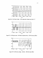
Input current drawn by an ASD at 100% load (one phase shown)
39
5.2 Input phase voltage, 2% single-phase sag on phase "a"
41
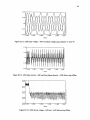
5.3 ASD dc-bus voltage, 2% single-phase sag, no load (at 0.02 seconds)
42
5.4 Input current, 2% single-phase sag, no load (phases "a" and "c" shown)
42
5.5 ASD dc-bus voltage, 2% single-phase sag, 50% load
43
5.6 Input current, 2% single-phase sag, 50% load (phases "a" and "c" shown)
43
5.7 ASD dc-bus voltage, 2% single-phase sag, full load
44
5.8 Input current, 2% single-phase sag, full load (phases "a" and "c" shown)
44
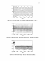
5.9 Input current, 5% single-phase sag, 50% load
46
5.10 Input current, 5% single-phase sag, full load
47
5.11 Input current, 10% single-phase sag, 50% load
48
5.12 Input current, 10% single-phase sag, full load
49
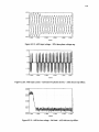
5.13 Input current, 13% single-phase sag, 50% load
50
5.14 Input current, 13% single-phase sag, full load
51
LIST OF FIGURES (Continued)
Figure
5.15 Input current, 17% single-phase sag, 50% load
52
5.16 Input current, 17% single-phase sag, full load
53
5.17 ASD input voltage - 90% single-phase voltage sag
58
5.18 ASD input current
58
full load (two phases shown)
5.19 ASD dc-bus voltage
full load
58
5.20 ASD input voltage
100% single-phase voltage sag
59
5.21 ASD input current
full load (two phases shown)
60
5.22 ASD dc-bus voltage
full load
60
5.23 ASD input voltage
50% two-phase voltage sag
61
5.24 ASD input current
full load (two phases shown)
61
5.25 ASD dc-bus voltage
full load
62
5.26 ASD input voltage
50% three-phase voltage sag
63
5.27 ASD input current
no load (two phases shown)
63
5.28 ASD dc-bus voltage
5.29 AWG test setup
no load
63
three-phase 480Hz capacitor switching transient
5.30 Output of programmable source
three-phase 480Hz capacitor switching transient
5.31 Output of programmable source with 10% voltage total harmonic distortion
64
64
77
LIST OF TABLES
Table
2.1 Measurement display formats for PQ power analyzer
13
3.1 AWG data transfer driver profile blocks
22
3.2 AWG file creation driver profile blocks
23
3.3 AWG setup and operation driver profile blocks
23
5.1 Data from a 2% single-phase sag
39
5.2 Data from a 5% single-phase sag
45
5.3 Data from a 10% single-phase sag
47
5.4 Data from a 13% single-phase sag
49
5.5 Data from a 17% single-phase sag
51
5.6 Summary of single-phase sag testing
54
5.7 90% single-phase voltage sag results
57
5.8 100% single-phase voltage sag results
59
5.9 50% two-phase voltage sag results
61
5.10 50% three-phase voltage sag results
62
5.11 95% single-phase voltage sag results
65
5.12 100% single-phase voltage sag results
66
5.13 50% two-phase voltage sag results.
66
5.14 50% three-phase voltage sag results
67
5.15 63% single-phase voltage sag, phase "a," regular configuration
69
5.16 65% single-phase voltage sag, phase "a," regular configuration
69
5.17 100% single-phase voltage sag, phase "a," regular configuration
70
5.18 30% two-phase voltage sag, phases "a" and "b," regular configuration
71
5.19 20% two-phase voltage sag, phases "b" and "c," regular configuration
71
5.20 20% three-phase voltage sag, regular configuration
72
5.21 50% two-phase voltage sag, phases "b" and "c," modified configuration
72
5.22 30% three-phase voltage sag, modified configuration
73
5.23 Summary of ASD Ride-Through Results
75
LIST OF APPENDICES
Appendix A Procedure to Operate/Program AWG
87
Appendix B LabVIEW Individual Function Blocks
93
Appendix C LabVIEW Instrument Driver Profile Blocks
95
Appendix D Procedure to Create New Instrument Driver Profile Blocks
105
Appendix E ASD Ride-Through Characterization Figures
109
El. 11 kVA ASD
Internal Power Supply Derived from DC Bus
109
E2. 5.5kVA ASD
Internal Power Supply Derived from 1-Phase Transformer
114
E3. 5.5kVA ASD
Internal Power Supply Derived from 3-Phase Transformer
122
LIST OF APPENDIX FIGURES
Figure
Cl. 1
Front panel window for Query Internal Memory profile block
95
C2. 1
Front panel window for Upload All Waveform Files profile block
95
C3. 1
Front panel window for Upload Waveform File profile block
96
C4.1
Front panel window for Upload All Sequence-Equation Files profile block
96
C5. 1
Front panel window for Upload Sequence-Equation File profile block
97
C6. 1
Front panel window for Download Waveform File profile block
97
C7. 1
Front panel window for Download Sequence-Equation File profile block
98
C8. 1
Front panel window for Define-Compile Equation profile block
98
C9. 1
Front panel window for Define Sequence File profile block
99
Cl 0.1 Front panel window for General Command profile block
100
Cli. 1 Front panel window for Load All Channels profile block
101
C 12.1 Front panel window for Set Operation Mode profile block
102
C 13.1 Front panel window for Set Channel Output profile block
103
Cl4.l Front panel window for Execute Trigger profile block
Dl.l Front panel window of standard subsystems in a profile block
104
D1.2
Block diagram window of standard subsystems in a profile block
105
D2. 1
Program diagram window of a multiple subsystem profile block
107
105
D2.2 Program diagram window of a command string to write profile block
107
D3.l Example icon connector
108
El.l ASD input voltage 95% single-phase voltage sag
109
El.2 ASJ) input current full load (two phases shown)
109
E1.3
ASD dc bus voltage
109
E1.4
ASD input voltage
-
full load
100% single-phase voltage sag
110
El.5 ASD input current full load (two phases shown)
El.6 ASD dc bus voltage full load
110
E1.7
ASI) input voltage
111
Ei.8
ASD input current full load (two phases shown)
50% two-phase voltage sag
110
lii
El.9 ASD dc bus voltage full load
El.10 ASD input voltage 50% three-phase voltage sag
112
El. 11 ASD input current
112
no load (two phases shown)
E1.l2 ASDdcbusvoltagenoload
111
112
LIST OF APPENDIX FIGURES (Continued)
Figure
El. 13 ASD input voltage
capacitor switching transient
113
El. 14 ASD input current
full load (two phases shown)
113
E1.15 ASD dc bus voltage
E2. 1
full load
113
ASD input voltage 63% single-phase voltage sag on phase "a"
114
E2.2 ASD input current full load (phases "b" and "c" shown)
114
E2.3 ASD dc bus voltage
114
full load
E2.4 ASD input voltage 65% single-phase voltage sag on phase "c"
115
E2.5 ASD input current full load (phases "b" and "c" shown) - ASD tripped offline
115
E2.6 ASD dc bus voltage full load ASD tripped offline
115
E2.7 ASD input voltage 65% single-phase voltage sag phase "a"
116
E2.8 ASD input current full load (two phases shown) ASD did not trip offline
116
E2.9 ASD dc bus voltage full load ASD did not trip offline
116
E2.lO ASD input voltage
117
100% single-phase voltage sag on phase "a"
E2. 11 ASD input current full load (two phases shown) ASD did not trip offline
117
E2.12 ASD dc bus voltage
117
full load ASD did not trip offline
E2.13 ASD input voltage
30% two-phase voltage sag on phases "a" and "b"
118
E2.14 ASD input current
full load (two phases shown) ASD did not trip offline
118
E2.15 ASD dc bus voltage
full load ASD did not trip offline
118
E2. 16 ASD input voltage
20% two-phase voltage sag on phases "b" and "c"
119
E2. 17 ASD input current
full load (two phases shown) ASD did not trip offline
119
E2.18 ASD dc bus voltage
E2.19 ASD input voltage
full load ASD did not trip offline
20% three-phase voltage sag
119
120
E2.20 ASD input current full load (two phases shown) ASD did not trip offline
120
E2.21 ASD dc bus voltage
120
E2.22 ASD input voltage
full load ASD did not trip offline
capacitor switching transient
121
E2.23 ASD input current (full load) capacitor switching transient
121
E2.24 ASD dc bus voltage (full load)
121
E3. 1
ASD input voltage
50% two-phase voltage sag on phases "b" and "c"
E3.2 ASD input current full load
E3.3 ASD dc bus voltage
capacitor switching transient
(two
phases shown) ASD did not trip offline
full load ASD did not trip offline
E3.4 ASD input voltage 50% three-phase voltage sag
122
122
122
123
LIST OF APPENDIX FIGURES (Continued)
Figure
E3.5 ASD input current full load (two phases shown) ASD did not trip offline
123
E3.6 ASD dc bus voltage full load ASD did not trip offline
123
LIST OF APPENDIX TABLES
Table
A 1.1 AWG channel configuration
87
B1
AWG2005 Individual quely function blocks
93
B2
AWG2005 Individual action function blocks
93
A REMOTELY CONTROLLED POWER QUALITY TEST PLATFORM
FOR CHARACTERIZING THE RIDE-THROUGH CAPABILITIES OF
ADJUSTABLE SPEED DRIVES
1.
1.1.
INTRODUCTION
What is Power Quality?
Power quality has become an issue of increasing concern to both electric utilities and end
users of electrical power since the 1 970s. The term "power quality" is applied to a wide range of
electromagnetic phenomena that cause voltage and current non-idealities to occur on a power
system [1]. A description of a power quality problem is defined in [1] as: A power quality
problem is any power problem manifested in voltage, current, or frequency deviations that results
in failure or misoperation of customer equipment. A definition of power quality is also given by
the IEEE Recommended Practice for Powering and Grounding of Sensitive Electronic
Equipment, IEEE Standard 1100-1992, as: Power quality is the concept of powering and
grounding sensitive equipment in a manner that is suitable to the operation of that equipment [2].
There are several reasons for the heightened interest in power quality issues both by utilities
and consumers. The use of electronic and power electronic equipment has proliferated in both
industrial and commercial applications.
In addition to becoming more widely used, this
equipment is increasingly sensitive to voltage disturbances, leading to loss of production time and
thereby a reduction in company profit margins. Power electronic equipment also causes voltage
and current disturbances for other customers and equipment. In particular, an increased use of
converter-type, nonlinear load equipment, ranging from computer power supplies to adjustable
speed drives, has increased the level of current and voltage distortion seen on the power system
[2-4]. Interest in power quality is also more important under the deregulation of the electric
utility industry. In an open competition market, customers can choose their supplier of power.
With no clear definition of responsibility for power quality and reliability, utilities are striving to
deliver power with a high reliability to meet customer expectations, yet do so in an economical
manner [2, 5].
Among consumers, power quality is important to sensitive and disturbing loads of all levels,
including residential, commercial, and industrial users. One area of particular interest, termed the
"digital economy," has been the development and growth of microprocessor based integrated
circuit applications, ranging from computers to phones to programmable logic controllers (PLCs).
2
Many of these microprocessor based products are part of a larger infrastructure such as digital
networks, the internet, and broadband telecommunications which demonstrate just a few
examples of customers with increasingly exacting demands for power [5]. According to the
Electric Power Research Institute (EPRI), information technology accounts for 13% of the
electricity consumption in the U.S., and they believe that it may grow to 50% in the next twenty
years [5-6].
The main motivator behind improving power quality is economic. An increased reliability of
electrical power (ideally for microprocessors, to 9-nines reliability, or 99.9999999% reliability)
equates to increased productivity and profit margins. As an example, at Sun Microsystems Inc. in
Palo Alto, California, outages are estimated to cost the company $1 million per minute due to lost
production. Overall, EPRI estimates that lost productivity and downtime, ranging from system
malfunction, product loss, and hardware damage to costly data loss, due to power outages, costs
the United States $50 billion annually [7]. In an effort to better understand the link between
power reliability and economic productivity and to demonstrate technological solutions to current
problems that threaten this linkage, EPRI began operation of the Consortium for Electric
Infrastructure to Support a Digital Society (CEIDS) in January 2001.
CEIDS membership
includes utilities, equipment manufacturers and representatives of industrial groups that are
particularly sensitive to power quality. A main task of CEIDS will be to determine which
combination of technologies is likely to be most cost-effective in optimizing power quality [5].
Power quality disturbances can be described according to the following categories [1-2, 8-9]:
Transients: A transient is a power system variation that is undesirable but momentary in nature.
A transient is characterized by a sudden change in the steady-state condition of voltage, current,
or both that follows an impulsive or oscillatory behavior. Transients can last anywhere from just
a few nanoseconds up to 30 cycles in duration, oscillate in a frequency range from a few kHz up
to a few MHz, and peak in magnitudes of up to 5 per unit (pu). Typical causes of transients are
lightning strikes and capacitor switching operations.
Short Duration Variations: A short duration variation is either a temporary voltage drop (sag,
dip), voltage rise (swell), or complete loss of voltage (interruption). An interruption occurs when
the supply voltage or load current decreases to less than 0.lpu for less than one minute. A sag is
a decrease in rms voltage or current at the nominal frequency to between 0.1 and 0.9pu.
Conversely, a swell is an increase in rms voltage or current at the nominal frequency to between
3
1.1 and 1 .8pu. Voltage sags and swells typically last anywhere from under a cycle up to a couple
of minutes. Short duration variations are typically caused by system fault conditions, short
circuits, circuit breaker reclosure operations, overloads, the energizing of large loads that require
high starting currents, or intermittent loose connections in power wiring.
Long Duration Variations: A long duration variation is a sustained overvoltage, undervoltage
(brownout), or interruption lasting longer than two minutes. Long duration variations are caused
by load variations on the system, system switching operations, and voltage regulation equipment
such as tap settings on transformers.
Voltage and Phase Unbalance: Voltage unbalance is the maximum deviation from the average
of the three-phase line-to-line voltage, divided by the average of the three-phase line-to-line
voltage. Phase angle unbalance is the deviation from the normal 120 or 240 degrees between
three-phase voltages [10]. Voltage and phase unbalance is caused by unequal loading of singlephase loads on a three-phase system.
Waveform Distortion: Waveform distortion is a steady-state deviation from an ideal sine wave.
Four primary types of waveform distortion are dc offset, harmonics, interharmonics, and
notching.
Voltage harmonic distortion is usually less than 20%, while current harmonic
distortion is usually less than 100%. The main contribution to harmonic voltage and current
distortion is due to nonlinear loads which draw a nonsinusoidal current. Some of the effects of
voltage and current harmonics are heating losses, interference leading to misoperation of solid
state devices, and additional stresses on system capacitors.
Interharmonics are caused by
equipment such as cycloconverters and arc furnaces. Normally, they do not cause significant
problems, but sometimes can lead to saturation of transformers, resonances between transformers
and capacitors, and subsynchronous resonance in synchronous generators.
Voltage Fluctuations: Voltage fluctuations are systematic variations of voltage or a series of
random voltage changes of relatively small magnitude, typically less than 0.1 pu.
Voltage
fluctuations are also referred to as flicker and noise. Loads creating continuous, rapid variations
in the load current magnitude cause voltage fluctuations.
Power Frequency Variations: Power frequency variations are the deviation of the power
system fundamental frequency from its nominal value (typically 60 Hz). Power system frequency
4
is directly related to the speed of the generators supplying the system. Therefore, significant
frequency deviations on a large power system are rare. Frequency deviations could be caused on
an isolated generator-load system due to inadequate governor response to abrupt load changes.
The main goal of electric utilities and end-use customers is to minimize the number of power
quality problems. This can be achieved by limiting the amount of power quality disturbances
caused by equipment, by improving the performance of the power system, and by making
equipment less sensitive to power quality disturbances.
1.2.
Harmonic Distortion
Harmonic distortion of voltage and current results from the operation of nonlinear loads and
devices in a power system. A nonlinear load is one in which the current is not proportional to the
applied voltage. Nonlinear loads draw currents whose frequencies differ from the frequency of
the source. Nonlinear loads that cause harmonics can often be represented as current sources of
harmonics. The system voltage appears stiff to individual loads and the loads draw distorted
current waveforms [3, 8]. Harmonic generating loads that are commonly used in residential,
commercial, and industrial applications are listed below.
Adjustable speed drives
Switch-mode power supplies
Uninterruptible power supplies
Silicon-controlled rectifier (SCR) drives
Arc furnaces and welders
Air conditioners and compressors (HVAC)
Elevators
Fluorescent lighting (electronic ballasts)
Most of these harmonic generating loads consist of solid state rectifiers at their inputs
connected to a dc-bus maintained by capacitors.
Solid state rectifiers draw current in pulses
when the input ac line voltage is higher than dc-bus voltage across the capacitors. As current
harmonics are injected back into the system, voltage drops are caused at the corresponding
harmonic frequencies, creating voltage distortion in the power system. The voltage distortion is
directly proportional to the current harmonic magnitudes and the impedance in the system (cables
and transformers) [9].
Some common effects of harmonic distortion are listed below [1,3,9,11].
5
Harmonic voltage stress on system capacitors and equipment capacitors
Resonance and overloading problems with power factor correction capacitors
Additional heating and losses in conductors, transformers as well as induction and
synchronous machines
Interference with communications circuits
Misoperation of circuit breakers, PLCs, computers, and other sensitive solid state loads
Voltage distortion at the PCC
According to IEEE 519
IEEE Recommended Practices and Requirements for Harmonic
Control in Electrical Power Systems, harmonic limits are meant to be applied at the point of
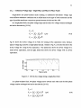
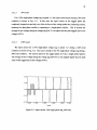
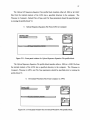
common coupling (PCC) between the utility system and multiple customers (Fig. 1.1) [12]. A
two way responsibility has been proposed for controlling harmonic levels on the power system.
Customers must limit harmonic currents injected into the power system.
.
Utilities must control the harmonic voltage distortion by making sure system resonant
conditions do not cause excessive magnification of the harmonic levels.
pCC
Utility System
Customer Under Study
Other Utility
Customers
Utility System
PCC
Other Utility
Customers
Customer Under Study
Figure 1.1: Power system showing location of the PCC where other customers can be supplied.
The following expressions are commonly used to indicate the harmonic distortion of a
waveform [13]. The total harmonic distortion (THD) can be calculated as a percentage for either
a voltage or current waveform.
THD=
h=2
I'
xl00%
(1.1)
The magnitude of the individual harmonic components is 'h, where h is the harmonic order,
and I is the r,ns-value of the fundamental current component. In some cases THD may not be a
very good indicator of the amount of current waveform distortion in a system. This is true for
circumstances where the current distortion of a light load may be very high, yet would not have a
significant impact on the power system. IEEE Standard 519-1992 uses total demand distortion to
evaluate the level of distortion in voltage and current waveforms.
h=2
TDD,
xl00%
(1.2)
The total demand distortion (TDD) is the THD of the current, using a 15-30 minute averaging
measurement period, normalized to the maximum rms-value demand load current 'L (fundamental
component, 60Hz). The TDD allows harmonic currents to be evaluated over a wide range of load
conditions with a constant base value. Additional expressions commonly used to describe
measures of power quality in a power system are displacement power factor (DPF) and true
power factor (PF).
DPF=cosO
I
(1.3)
I
(1.4)
(1.5)
7
In the above equations, I is the rms-value of the fundamental component of the current, I is
the total rms-value of the current, and 0 is the phase angle between the voltage and current.
Another expression used to indicate the additional eddy current heating losses in a transformer
due to current harmonics is the K factor [9, 14].
K=
Ih
h
(1.6)
The K factor equation (1.6) indicates that transformer heating losses are proportional to the
square of the load current and the square of the frequency.
1.3.
Harmonic Distortion Mitigation Techniques
Harmonic distortion in a power system can be controlled and negatively affected equipment
can be protected according to several different methods. One method involves resizing or adding
components to protect sensitive equipment. Examples of this are the use of larger phase and
neutral conductors, derating of transformers and motors, use of K-rated transformers, and proper
sizing and de-tuning of capacitors [9, 15].
Another method is to purchase equipment with reduced harmonic generation. This is usually
an initial option that is difficult and costly to implement with pre-existing equipment.
An
example of this is the application of line reactors (inductive chokes) in series with the ac input of
nonlinear loads such as adjustable speed drives (ASDs) [9, 16]. Adding a line reactor in series
with the ASD will reduce current harmonics and provide transient protection benefits. However,
a slight voltage drop is then seen at the input of the ASD rectifier. Sometimes, a reactor is added
to the dc-link of an ASD which then eliminates the ac voltage drop, but does not provide as much
overvoltage transient protection. Other examples of equipment with reduced harmonic generation
are ASDs with higher pulse numbers. A six pulse ASD generates predominantly fifth and
seventh harmonics.
Whereas a twelve pulse ASD generates predominantly eleventh and
thirteenth harmonics, and the magnitudes of these harmonics are much lower [9].
Applying technologies that cancel harmonics from different loads is another method for
eliminating harmonics. This is commonly achieved with standard transformer connections [1718].
Transformers can reduce harmonics in two ways, through harmonic attenuation and by
harmonic cancellation. Transformers have a reactive impedance which increases directly with
frequency, naturally attenuating harmonics. Harmonic cancellation occurs when two or more
8
three-phase loads are phase-shifted from one another through various types of three-phase
transformer connections. The sum of the current drawn is then less distorted than the original
nonlinear current drawn by each individual load. For example, in a system with several ASD
loads, some loads can be supplied by delta-delta connected transformers and other loads can be
supplied by delta-wye connected transformers. If the loads on each drive isolation transformer
are balanced, harmonic current distortion can be significantly reduced. In some applications
where a neutral point for grounding is desired, a delta-zigzag transformer provides the same
harmonic cancellation effect when used with loads also supplied by a delta-wye connected
transformer.
Filtering is another method for reducing harmonic currents in a power system.
Many
topologies of harmonic filters are used with three general categories being passive, active, and
hybrid filters [3, 9, 15, 19-20]. Passive filters consist of tuned LC filters which can be connected
in shunt or in series at a point where nonlinear loads are concentrated or at an individual
nonlinear load. They can be tuned to block or trap single frequencies or multiple stages can be
used for more than one frequency. A shunt passive filter creates a low impedance path for
harmonic currents at its tuned frequency, thereby trapping or diverting the harmonic current from
flowing into the power system. A series passive filter creates a high impedance at its tuned
frequency, thereby blocking the flow of harmonic currents into the power system.
Passive filters
must be carefully designed and derated to allow for harmonics also absorbed from the power
system as well as possible resonance problems with power factor correction capacitors. Active
filters monitor the load current to be filtered and use pulse width modulation inverter technology
to inject compensating current equal to the load harmonic current, but with the opposite phase, in
order to cancel the harmonic currents flowing in the power system.
Hybrid filters use a
combination of both passive and active filters to cancel load harmonics with the goal of reducing
initial costs and component rating requirements enabling their use for high power nonlinear loads.
1.4.
Research Project
With the increased attention on high efficiency and controllability of industrial processes, as
well as reduced weight, volume and cost of consumer products, the applications of power
electronic converters such as adjustable speed drives (ASDs), switch-mode power supplies, and
programmable logic controllers (PLC5) are showing a rapid rise. Investigating and mitigating
power quality issues pertaining to the input supply of power electronic equipment are extremely
important in maintaining a high level of reliability and productivity. In response to these
9
concerns, a number of approaches are being undertaken to improve power system quality and
reduce equipment susceptibility to power quality disturbances.
Obviously, much research, both theoretical and experimental, is being done to develop power
conditioning and backup generation technologies, equipment with increased power quality
disturbance ride-through capability, as well as technologies to improve utility power delivery
systems. The market is growing with products that protect power electronic equipment from
voltage sags, transients, and interruptions. On the utility side, dynamic voltage regulators
mitigate voltage sags at high power, medium voltage levels. Companies such as General Electric,
Toshiba, Square D, ABB, and Electrotek Concepts all develop power quality protection
equipment targeted toward sensitive industrial customers. For example, Electrotek Concepts has
developed the Dynamic Sag Corrector (DySC) which protects equipment ranging in size from
l.5kVA to 2000kVA with a minimal size, low cost, and high level of efficiency [21]. Square D
has recently come out with its REACTIVAR Electronic Sag Protector which performs the same
functionality as the DySC [22].
Other steps include the development of standards such as IEEE 519, which recommends
operational guidelines for electric utilities and end-use consumers. The creation of task forces to
address power quality issues such as EPRI's CEIDS consortium is another example of a method
for advancement of power quality issues. The development of power monitoring equipment with
the ability to measure both rms and transient waveforms and capture power quality disturbances
is another component toward understanding and quantifying the need for mitigation equipment
under various circumstances.
Another important approach toward understanding how power quality disturbances affect
power electronic equipment is the ability to experimentally capture and also create various
disturbances typically seen in industrial and commercial environments. This would provide a
controlled environment enabling the characterization of power electronic equipment performance,
as well as a platform to test power quality protection technologies. The objective of this thesis
research is to design and implement a power quality test platform (PQTP) with these capabilities.
The PQTP incorporates a 12OkVA three-phase programmable voltage source with the capability
to drive single and three-phase loads.
The PQTP is controlled by an arbitrary waveform
generator (AWG) which enables a versatile and independent configuration of each output voltage
phase.
10
Organization of Thesis
1.5.
The thesis is organized according to the following description of chapters. Chapter 1
provides background information on power quality and why it is an important issue among
electric utilities and end-use consumers. Also discussed are the classifications of power quality
disturbances, causes and effects of waveform harmonics, and mitigation techniques for waveform
harmonics. The defmition of the thesis research project is also summarized.
In Chapter 2, the equipment configuration of the power quality test platform is described.
The test capabilities of the power quality test platform are outlined and the general operation and
control of the test platform is explained.
Chapter 3 provides a short overview of the LabVIEW programming environment. Also
presented is a detailed description of the development of a LabVIEW driver database which is
used to program, monitor, and control the power quality test platform's arbitrary waveform
generator.
Included in Chapter 4 is an explanation of the architecture of a three-phase voltage source
inverter adjustable speed drive.
Also described is the theoretical background behind the
susceptibility of ASDs to voltage sags. Additionally, methods for improving ASD ride-through
capability are presented.
Chapter 5 presents experimental results of ASD ride-through characterization obtained from
testing with the power quality test platform.
Comparisons are made between different
architectures of ASDs and ride-through performance is evaluated for multiple types of voltage
sags.
Finally, Chapter 6 is the concluding chapter where experimental and theoretical ASD ride-
through results are discussed. Also future work and recommendations are made pertaining to
both the power quality test platform capabilities and ASD ride-through research.
11
POWER QUALITY TEST PLATFORM
2.
2.1.
Equipment Setup
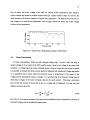
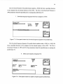
The power quality test platform (PQTP) has been implemented in the Motor Systems
Resource Facility (MSRF) at Oregon State University as shown in Fig. 2.1. The input of the
programmable source is protected through a 200A circuit breaker and the output is directly wired
to a three-phase terminal connection box. The output terminal connection box consists of several
types of connectors enabling a variety of test loads to be fed from the programmable source. A
PQ power analyzer is configured between the output of the programmable source and the input of
the test load. The PQTP has been installed such that either of the MSRF test beds can be supplied
by the programmable source, in addition to several of the laboratories in the Dearborn Hall
basement. For the purpose of this thesis, all experimental work has been performed with the 1 5hp
test bed used as a test load for the PQTP.
Dedicated
Utility Supply (750 IIVA)
I
+
MCC-1
I)
I)
Control
Circuit
Auto
480: 0 to 600
Transformer
MCC-2-.
L5Locked
j Rotor
L
)500 hp j350 Op
I,
L
I.
J
250 Op
L
I.
)125 lip )50 lip
Motor (600 lip)
Starter
)30 lip
[Motor (50 lip)
Starter
L __
[I1
IS lip Test 6.0
500 lip Teat Bed
(ASDI.oiotors..tc)
Figure 2.1: Schematic of MSRF including the Power Quality Test Platform.
12
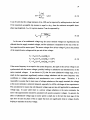
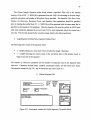
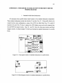
A more detailed representation of the PQTP is shown in Fig. 2.2. The main hardware and
instmmentation comprising the PQTP includes the three-phase programmable source with an
integrated arbitrary waveform generator (AWG), a PC for remote control of the AWG, and a
three-phase power analyzer with event capture/data logging capabilities.
2.2.
Three-Phase Programmable Source
The 12OkVA three-phase programmable power source is a one-of-a-kind unit made by
Behlman Electronics Inc. that enables a flexible, variable amplitude and frequency output [23].
The programmable source is composed of three solid state converters (one per phase) supplied
from a multi-tapped input transformer to provide a wide range of output capabilities. Each power
amplifier has an output range of O-l32Vac rms. The output of the power amplifiers is stepped up
through a transformer that enables a rated output voltage range of O-3O5Vac rms, line-to-neutral,
a current limit of 144A rms per phase, and a frequency range of 45Hz to 2kHz. Peak voltage
capabilities are O-460V instantaneous line-to-neutral and peak current capabilities are 2.9 times
the rms rating [23-24]. A Sony/Tektronix model AWG2005 arbitrary waveform generator
(AWG) has been custom integrated with the programmable source. The AWG has four output
channels, three of which are used to represent the desired three output power phases, while the
fourth channel is used as a trigger source. The AWG channels have an output range from 0-by
that are amplified and correspond to a 0-326Vac rms line-to-neutral (0-564V rms line-to-line)
output range of the programmable source [24].
PCwith
LabVIEW
instrument driver
I
I
OPtS irrerleer
I
120k VA
Programmable
Source
lOtech/ESA
three-phase
Test Loads
(ASDs, motors, etc.)
Figure 2.2: Block diagram of the Power Quality Test Platform (PQTP).
13
2.3.
Three-Phase PQ Power Analyzer
The PQTP includes a three-phase power analyzer, model PowerVistal3 12 by lOtech, Inc.
The power analyzer consists of a data acquisition box, laptop PC, and EasyPower Measure
Windows software developed by ESA, Inc. The power analyzer monitors and captures voltage
and current information and can calculate and display all relevant quantities (V, I, kW, kVAR,
kVA, pf, THD, etc.) in a waveform, phasor, or Fourier analysis format. The power analyzer has
four differential voltage channels as well as four external shunt current channels enabling three-
phase power measurements as well as two additional parameter measurements at important test
points.
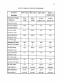
The EasyPower Measure software has five measurement display and data logging formats.
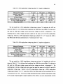
Table 2.1 gives a short description of the different measurement formats [25].
Table 2.1: Measurement display formats for PQ power analyzer.
Measurement Format
Description
Phasor Diagram
Single cycle measurement with real time
display update of all fundamental and rms
quantities, good for quick viewing.
Detailed Harmonics
Captures 10 cycles of waveform data and then
performs a harmonic decomposition of the data
for all signals.
Spectrum Analyzer
Performs spectral decomposition on a single
waveform captured from a selected input
channel.
Cycle-by-Cycle Capture
Event Capture
Cycle by cycle measurement and data logging
of all fundamental and rms quantities enabling
detailed trending of all quantities.
Continuously
monitors
all
channels
and
captures sub-cycle events while continuously
logging information.
The event capture mode of the PQ power analyzer is very useful for capturing power quality
disturbances simulated with the PQTP. In this mode, the PQ power analyzer saves data when
triggered according to pre-selected setpoints. The event capture mode of the PQ power analyzer
14
monitors all channels and captures event information for a specified time interval. Events are
triggered when one or more of the following specified trigger thresholds is exceeded:
Peak Trigger
Maximum Trigger - mis
Minimum Trigger - rms
Delta Trigger - rms
Slope Trigger
THD Trigger
Zero Crossing Trigger
2.4.
AWG Operation
The AWG enables a flexible programming method for generating power quality disturbances.
The AWG has several different modes of operation as well as several different mechanisms for
creating waveforms. Waveforms can be created either from standard function blocks combined
with mathematical permutations, or from an equation, or from data downloaded from another
instrument [26]. The two modes of operation that are useful in simulating multiple types of
voltage disturbances are the continuous and waveform advance modes. The continuous mode
repeats a group of waveforms continuously at a set clock frequency rate. Examples of continuous
mode waveforms would be in simulating a nominal voltage condition or steady-state power
quality disturbance scenario such as voltage magnitude and phase unbalance or voltage harmonic
distortion. The waveform advance mode outputs a sequence of waveforms according to a given
trigger command. Examples of waveform advance mode waveforms are transient power quality
disturbances such as several cycle voltage sags or capacitor switching transients. A tutorial on
the operation and programming of the AWG for generating both steady-state and transient power
quality disturbances is given in Appendix A.
2.5.
Lab VIEW Instrument Driver
An attractive feature of the programmable source's AWG is its ability to be remotely
programmed and controlled through a GPIB interface. A command driver database has been
created and tested using National Instruments Lab VIE W, which contains the functionality
necessary to conduct a wide range of power quality tests using the programmable source.
15
2.6.
PQTP Operation
The programmable source can be operated with or without the AWG controlling the output
voltage. Without the AWG "programming" the source output, the balanced sinusoidal three-
phase voltage magnitude and frequency can be manually adjusted. The output is applied to the
test load and monitored by the PQ power analyzer. When the AWG is not programming the
source output, the source cannot be controlled via computer with the LabV1EW/GPIB interface.
When the AWG does program the output voltage of the source, each of the three output phase
corresponding channels must have a different waveform or sequence file loaded and their output
turned on. In the continuous operating mode, the output of the AWG is amplified by the source
and output to the test load. In the waveform advance mode, a nominal waveform is continuously
output by the AWG. The nominal waveform is amplified by the source and output to the test load
until the trigger signal is applied to the AWG. The trigger signal can be executed manually or
remotely from the LabVIEW interface. The trigger signal causes the waveforms in the sequence
following the nominal waveform to each cycle one time in consecutive order. After the last
waveform in the sequence has been executed, the output of the AWG returns to the continuous
output of the initial nominal waveform [26].
The entire cycle of a waveform advance mode sequence can be captured by the PQ power
analyzer. One or more event mode trigger parameters can be setup to match the particular power
quality disturbance programmed in the waveform advance mode sequence. The number of cycles
of data to capture and record after the triggered event can also be user-defined. The maximum
possible event length recorded to a data file is 28800 points. With a set sampling rate of 128
points per cycle, 225 cycles at 60Hz can be recorded to a data file. The number of event capture
data files is only limited by the laptop PC hard drive disk capacity [25].
16
3.
3.1.
LABVIEW INSTRUMENT DRIVER FOR AWG
Introduction
Initially, all of the programming setup for the arbitrary waveform generator (AWG) was
performed manually through the front panel interface. Most of the functionality available through
the front panel interface can be programmed remotely through the AWG's GPIB communication
port. National Instruments' LabVIEW was chosen as the software interface for programming the
AWG remotely. Lab VIEW has a descriptive front panel graphical user interface and is used as a
standard data acquisition and control program for most instrumentation in the MSRF at OSU.
LabVIEW also has the capability for remote data acquisition and control over the internet,
enabling future coordination work with other research facilities and universities.
3.2.
Lab VIEW Instrument Driver Objectives
Three main goals existed in the development of a LabVJEW driver database for the AWG
and programmable source. First, since the AWG has limited storage capabilities and has its
internal memory cleared whenever reset, the driver must provide a method for storing waveform,
equation, and sequence profiles and transferring these profiles to and from the AWG as they are
needed. Second, the driver must have the capability to create and modify the several types of
waveform, equation, and sequence files that are necessary to produce simulated voltage
disturbance conditions from the programmable source. And third, the driver must be able to
perform the control functions necessary to load, configure, execute, and trigger simulated voltage
disturbance conditions.
3.3.
Pre-Existing Instrument Driver
A Lab VIEW basic function driver database has been developed by National Instruments for a
similar Tektronix AWG, model AWG2O4 1.
Lab VIEW driver databases consist of virtual
instruments (VIs), each of which executes a specific function [27]. The VIs for a particular
device are grouped together in a library that is located within the LabVIEW instrument library
folder (instr.lib). The AWG2O41 instrument driver library consists of approximately fifty VIs
which are separated into five different categories.
One category initializes and closes
communication with the AWG. The other four categories include system configuration, action
17
and status, data collection and transmission, and utility functions.
Fig. 3.1 shows a tree
containing all of the VIs in the AWG2O4 1 instrument driver library.
To begin creating a LabVIEW driver database for the AWG2005, each of the VIs from the
AWG2O4 1 database was modified and reconfigured for the AWG2005. One difference between
the two AWG models is that the AWG2005 has four output channels compared to the AWG2O4 1
which has two output channels.
Therefore, much of the driver VI modification involved
incorporating additional functionality and changing the programming syntax that was different
between the two models [28].
Close
Initialize
Ai
Configuration
S.
S.
Action/Status
..,2041
.l
..,0041
Utility lJ
Data
Ek
..004
.204
.2041
.,004I
0d1
i(R
.n2041
-
..
041
.
0041
...,0041
....2041
...2041
LiH]
41:4I41
!H!41
..,004t
20!:
.2041
Figure 3.1: Tree of AWG2O4 1 instrument driver VIs.
LabYIEW Virtual Instrument Overview
3.4.
Lab VIEW is a general-purpose programming system with extensive libraries of functions and
development tools specifically designed for data acquisition and instrument control. LabVIEW
uses its own graphical programming language, G, to create programs in a block diagram form
[27].
Each VI consists of three main parts: the front panel, the block diagram, and the icon
connector. The front panel is the user interface and can be designed to simulate the instrument
front panel. The front panel can contain knobs, push buttons, graphs and other controls and
indicators where information is entered and displayed. The block diagram consists of executable
source code that is created using nodes, terminals, and wires. The VI receives instructions from
the block diagram in the form of function blocks, routines, and control elements that constitute
the VI code. A VI within another VI is called a subVl. The icon connector of a VI is a graphical
parameter list so that other VIs can pass data to a subVl. Figs. 3.2, 3.3, and 3.4 show the front
18
panel, block diagram, and icon coimector windows, respectively, for the AWG initialization VI.
This VI initializes communication with the AWG by writing the correct GPIB address in the
appropriate command string. An instrument reset can also be executed in this VI. Common to all
VI front panel windows are the "error in" and "error out" dialog boxes that help to troubleshoot
problems when multiple subsystems are used within a VI.
I
VISA Session
Instrument Descriptor
IGpI0 20 .INSTR
[iiJ
I
ID query
I
yes
too
ViSA Session (for class)I
I
Reset?
9es
error out
error in (no error)
rto
I
111
t
code
Illsttutus
code
Iisttutus
Iii
d0
d))
source
Isource
II
Figure 3.2: Front panel window for initialization VI.
Query ID nod device type registers
Reset instrument
Open instrument
0 qUery
insneiy
Instrument Desoiptor Ef-1
ISA Session (for doss)
ResetS
TrUe
.[
______
IiEAD OFFVER ONI
Instr
'.ISA Session
error in (no error)
10000
Send detnult setup
detnutt setup stung
error Out
IKfA20o51i.
VI noise
5InrnaIize23
Figure 3.3: Block diagram window for initialization VI.
Instrument Descriptor
ID query
Reset?
error in (no error)
ViSA Session
error out
Figure 3.4: Icon connector for initialization VI.
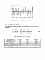
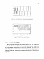
Another example of a very useful VI is the AWG picture capture VI. The front panel and
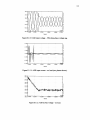
program diagram windows of this VI are shown in Figs. 3.5 and 3.6, respectively. This VI takes
a snapshot image of the AWG front panel display and sends the image in a specified format back
19
to the computer. The image can then be imported into the VI front panel window. In Fig. 3.5, the
imported image shows the AWG setup menu screen where file and configuration information
pertaining to the four output channels is displayed. In addition to determining which waveforms
are programmed into what channels of the AWG, the snapshot picture also enables many other
parameters of the AWG to be seen. Some of the other parameters include the clock frequency,
waveform operation mode, waveform amplitude, and output channel status. In this example, it
can be seen that nominal sinusoid waveforms have been loaded into the three output phase
channels, the clock frequency is set to 60kHz, the operation mode is set to continuous, the
amplitude of the three output phases is at 10.OV, and the output channels for the three phases are
turned on.
Dup VISA Session
VISA Session
Format
Port
error oul
SK
IBMP
Hard copyto:
Rselected port
computer
1stotus
error in (no error)
code
Ho
S1ource
Copy to lilepath
j
code
fl
sou roe
il
__________________
Continuous mode
GPIB
stots
I
Master Running
30-Apr-01 16:57:03
I Waveform
Sequence
.1
io.oeei,I
_______
U
II
Plormaj
U
I
CH2
I CH2
IJHJv_H
11hrou
11J1L
I
60. 00kHz
1.00ev
0.000V
DC_NOM.WFM
I
PHBNOM.
/""\\
Cu';
o cu
PKR_NOM.WFM
PHC_NOM.Ft.1
fthroug
8.08ev [1 0.00ev
QC C1
PHC_NOM.WFM
Clock
1
ation
Filter
Amplitude
Display
Offset
I
LiThli1
Text
Figure 3.5: Front panel window for AWG screen capture VI.
1
20
BMP
EPSO;
I1'F0RM
TH; iHCOPDATA?;WAI
I6OOOOO
vs;::n
RS232C1
errorin(noerror)
Hard co
to.
lOopy to iIepathI
r
error out
Figure 3.6: Program diagram window for AWG screen capture VI.
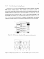
3.5.
Lab VIEW Profile Block Virtual Instruments
Since the AWG requires a specific order of instructions when operated remotely over a GPIB
interface, it is convenient to combine several of the common sequences of commands into profile
blocks. After several functional VI blocks had been created, it was possible to combine multiple
VIs together as subsystems and create profile blocks. Each profile block begins with an AWG
initialization VI and ends with an AWG close VI. In between are the functional VIs needed to
carry out a sequence of instructions. In most profile blocks, a snapshot image of the AWG screen
is displayed on the VI front panel since it is useful to be able to see exactly what is displayed on
the front panel screen of the AWG after a series of instructions has been performed.
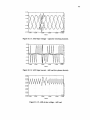
Profile blocks were created to enable the AWG to simulate power quality disturbances
entirely by remote operation as defined in the main objectives above. Figs. 3.7 and 3.8 show the
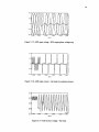
front panel and program diagram windows, respectively, of a simple profile block VI. The profile
block VI loads either waveform or sequence files into the four channels of the AWG and also
configures the file amplitude settings. The waveform or sequence files must already be stored in
the internal memory of the AWG. The front panel window shown in Fig. 3.7 has control
indicators for inpuuing the files to be loaded and their amplitudes for each channel, as well as
control indicators for the clock frequency and front panel image parameters. The program
diagram window shown in Fig. 3.8 contains subsystem VIs that load files and set parameters for
each AWG channel.
21
mm, oat
Image
Copy to
Foretet
Filopalh
\Evorr\TeroAWC\pore1 bop
IBtOrot
error in (no Boor)
de
I
mde
stOtrrs
MP
I
Renet?
Herd CopyTo
9Yot
ro Lond to Phone A)
rOflt Pnb
OspIny
kotoel
Continuous mode
CPIB
Master Runnin
m-apr-et 16:57:83
toT:
C113
::
npIrude-Phnoec(
aock
F6ter
AniplItude
Ottset
Figure 3.7: Front panel window for Load All Channels profile block.
DC Trugge
Lood fl Phose
n Phose BI
e - Phase ob
DC Tngge
IDCI
nueto Lood ifl]
_
Cj To
I
BC ____________ CC
(no error)!
ou
rontPerrn!DispIeyImeeI
to FiIepndh
Figure 3.8: Program diagram window for Load All Channels profile block.
3.6.
New Instrument Driver for AWG
Once the existing VIs were all functioning correctly with the AWG2005, additional VIs were
created to expand primarily the action and status, and data transmission capabilities.
This
included VIs to create and compile equation waveforms, create sequences of waveforms, load
files and operation mode setting into channels, and transfer files back and forth between the
computer and the AWG. A complete listing of the individual function VIs for the AWG2005
instrument driver library is provided in Appendix B.
22
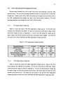
The profile blocks created can be divided into three groups as were defined in the main
objectives for the driver database. The first group of profile blocks includes storage and transfer
functionality to download and upload complete voltage disturbance event files to and from the
AWG. The second group of profile blocks includes the functionality to create new equations,
sequences and waveforms as well as modify existing files. The third group of profile blocks
includes setup and control functionality to load a voltage disturbance event, configure the mode
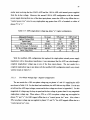
of operation settings, set the channel output, and control transient waveform generation. Tables
3.1, 3.2, and 3.3 show a listing and description of the profile blocks created for the AWG,
separated into the three main functionality groups.
Table 3.1: AWG data transfer driver profile blocks.
Virtual Instrument Profile Block
Functional Description
Upload All Waveform Files.vi
Transfers all files with a .WFM extension from the
internal memory of the AWG to a specified directory
in the computer.
Upload All Sequence-Equation Files.vi
Transfers all files with either a .SEQ or .EQU
extension from the internal memory of the AWG to a
specified directory in the computer.
Upload Waveform File.vi
Transfers a file with a .WFM extension from the
internal memory of the AWG to a specified directory
in the computer.
Upload Sequence-Equation File.vi
Transfers a file with either a .SEQ or .EQU extension
from the internal memory of the AWG to a specified
directory in the computer.
Download Waveform File.vi
Transfers a file with a .WFM extension from a
specified directory in the computer to the internal
memory of the AWG (file must have been previously
uploaded from the AWG).
Download Sequence-Equation File.vi
Transfers a file with either a .SEQ or .EQU extension
from a specified directory in the computer to the
internal memory of the AWG (file must have been
previously uploaded from the AWG).
Query Internal Memory.vi
Returns to the VI front panel window a catalog of
each file contained in the internal memory of the
AWG.
23
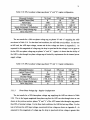
Table 3.2: AWG file creation driver profile blocks.
Virtual Instrument Profile Block
Functional Description
Defme-Compile Equation File.vi
Creates a .EQU
file from a given equation
expression, and also compiles the .EQU file into a
.WFM file according to an input number of
waveform points.
Create Sequence File.vi
Creates a .SEQ file from a given combination of
.WFM files and each associated number of repeat
cycles.
General Command.vi
Can be used to execute any combination of
waveform edit functions.
Table 3.3: AWG setup and operation driver profile blocks.
Virtual Instrument Profile Block
Functional Description
Load All Cbannels.vi
Loads either .WFM or .SEQ files into each of the
four AWG channels. Also sets channel parameters
including clock frequency, and amplitude.
Set Operation Mode.vi
Sets the AWG operation mode to either continuous
(used for steady-state waveform tests) or waveform
advance mode (used to simulate transient
disturbances).
Set Channel Output.vi
Turns the output of each of the four AWG channels
on or off.
Start-Stop Tngger.vi
Executes a trigger start operation. This is used in
waveform advance mode to trigger the transient
waveforms in the .SEQ files to execute and then
return to the nominal waveform set.
Each of the profile blocks described in Tables 3.1, 3.2, and 3.3 is more thoroughly referenced in
Appendix C. Appendix C shows the front panel windows for each profile block and gives an
explanation of how to configure the parameters in each profile block to execute power quality
disturbance simulations.
24
3.7.
Limitations in AWG Programming Functions
Some functionality necessaiy for complete programming and operation control of the AWG
does not have specific command syntax.
These functions include waveform edit mode
functionality. There is a general command set for the AWG which performs the same action that
actuating the corresponding AWG front panel key, button, or knob would do [28]. The general
command is ABSTouch and when it is combined with a combination of key, button, and knob
commands, will provide for a versatile range of AWG commands to be executed. For example,
writing the command "ABST SETUP" over the GPIB interface would display the same setup
menu that is displayed by pressing the AWG front panel SETUP button. The profile block
General Command.vi,
as seen in Table 3.2, was created to enable additional editing functionality
using the ABSTouch command.
In the future, it may be desirable to create new profile block VIs using the general command
VI and other combinations of functional VI blocks mentioned in the previous sections. The
flexible voltage and frequency capabilities of the programmable source will enable a large variety
of power quality tests to be performed. Given in Appendix D is a short tutorial on the basic
LabVIEW programming necessary to create new or modify existing profile block VIs.
3.8.
Programmable Source Range of Operation Limits for AWG
An advantage of programming and operating the AWG remotely through LabVIEW is the
ability to set protection limits and default values for the AWG and programmable source. The
output voltage range of the AWG in both amplitude and frequency can overextend beyond the
limits of the programmable source. This is because the AWG is designed as a general purpose
instrument and the amplitude range of the AWG was configured to allow for a peak instantaneous
voltage of O-460V line-to-neutral (rated instantaneous line-to-neutral voltage is 430V rms).
The
LabVIEW front panel interface allows for limits to be set on all function parameters.
Additionally, default settings can be set for all parameters and detailed help messages can also be
provided for any parameter.
The combination of these features significantly reduces the
possibility for incorrect operation of the programmable source beyond its intended ranges, and
also allows for a relatively simple and convenient setup effort for generating more commonly
tested power quality disturbances.
25
4.
4.1.
ADJUSTABLE SPEED DRIVE PROPERTIES
Adjustable Speed Drive Topology
Induction motors are the workhorse of industry due to their low cost and rugged construction.
Over the years, the integration of adjustable speed drives (ASDs) is increasing due to improved
efficiency, process control, and productivity. Earlier applications of ASDs were largely in fan
and pump loads where speed control resulted in significant energy conservation (with reported
values up to 35%) with very short payback times, and in these applications the dynamics of speed
control were not necessarily very fast or precise. More recently, the cost of ASDs has been
decreasing and their performance has been improving. Today, ASDs are used in many additional
industrial applications including semiconductor manufacturing, paper machines, winders,
extruders, metal casters, and overhead cranes [4,29].
Currently, 18% of all new motor
installations and 12% of existing motor systems in the U.S. are driven by ASDs [14].
Speed control of induction motors is commonly achieved through voltage source inverter
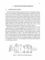
adjustable speed drives. The typical configuration of an ac ASD is shown in Fig. 4.1. At the
input is an uncontrolled three-phase diode bridge rectifier that supplies the dc-bus. The dc-bus
ripple voltage is minimized by the dc-bus capacitor. The dc-bus voltage is inverted to a variable
frequency, variable magnitude ac voltage by a pulse width modulated (PWM) inverter. The
speed of an induction motor can be varied by controlling the voltage frequency, f, applied to the
stator. For the torque capability to equal the rated torque at any frequency, the airgap flux should
be kept constant and equal to its rated value by controlling the magnitude of the applied voltage,
V, in proportion to the frequency. Over a large range of the motor torque-speed characteristic,
the V,/frelationship is linear [13].
Diode
Rectifier
dc link
PWM Inverter
Figure 4.1: Topology of an ac adjustable speed drive.
26
An ASD is considered a nonlinear load because the diode rectifier front-end draws nonsinusoidal current when supplied with a balanced sinusoidal input voltage. Typical ASD input
currents contain odd harmonics which can be determined by:
h=kq±l
The order of the harmonic is h,
k
(4.1)
is an integer beginning with k= 1, and q is the number of pulses
of the rectifier system. The topology of the ASD shown in Fig. 4.1 has a conventional "sixpulse" rectifier because the dc-bus voltage is defmed by portions of the line-to-line input voltage
that repeat with a 600 duration (one 360° cycle contains six pulses of the input voltage) [13-14].
Power quality problems associated with harmonics and harmonic mitigation technologies were
discussed in Chapter 1.
ASD Susceptibility
4.2.
As a critical component of manufacturing processes, ASD downtime due to offline tripping
caused by power quality disturbances contributes substantially to lost productivity and revenue
for industrial customers. Voltage sags, transients, and momentary interruptions of power together
constitute 92% of the power quality problems encountered by typical industrial customers,
according to a study sponsored by the Electric Power Research Institute (EPRI), in collaboration
with 24 utilities. Productivity loss due to deep voltage sags and brief power interruptions has
been called "the most important concern affecting most industrial and commercial customers
[21]."
The most common voltage sags are caused by single-line-to-ground faults. These types of
faults are caused by weather conditions, tree branches, animal contact, insulation failures,
automobile accidents or other human activity. A few customers near a fault may see a deep
voltage sag, followed by a complete interruption when utility circuit breakers clear the fault.
Most other customers connected through the same distribution or transmission system will see a
smaller voltage sag with the magnitude based on the customer's distance to the fault location as
well as intervening transformer connections that further isolate customers from the fault [2, 21].
Once the fault has been cleared or isolated, the system will return to nominal voltage.
The IEEE has developed a recommended standard that helps industrial power electronic
equipment users evaluate the impact of voltage sags at their facility: IEEE 1346-1998. This
standard describes a method for combining predictions of voltage sag magnitude, duration, and
27
rate of occurrence, with a characterization of equipment susceptibility to voltage sag events, to
determine the cost of voltage sag related downtime. The cost of incorporating either power
conditioning equipment or new process equipment with greater voltage sag tolerance can also be
compared with voltage sag related downtime costs [21].
Circumstances that can cause ASDs to trip offline are as follows [2, 14, 29-34]:
.
The ASD controller may be programmed to trip the drive offline upon detection of a sudden
change in operating conditions.
A voltage sag which leads to a drop in the dc-bus voltage may cause the ASD controller or
the PWM inverter to trip the drive offline.
A voltage sag which leads to insufficient voltage for maintaining the ASD's internal power
supply voltage used for powering control logic may cause the ASD to trip offline.
A voltage sag which leads to insufficient voltage for maintaining the ASD's external interface
and control circuitry such as contactors, relays, and PLCs.
A voltage sag can lead to an ASD overcurrent trip due to increased ac current drawn during
the voltage sag or due to high current spikes that charge the dc-bus capacitor immediately
following the voltage sag.
An ASD may trip due to motor changes such as a drop in speed or torque variations that the
load process cannot tolerate.
Of the six circumstances listed above that cause ASDs to trip offline, the two main causes are
reduced dc-bus voltage and reduced internal power supply and external circuitry voltage. During
voltage sag conditions, the motor/load power level, dc-bus capacitance, internal power supply
design, and dc-bus undervoltage trip level all affect whether or not the drive will trip offline. For
single-phase voltage sags, two of the phase-to-phase voltages are affected. Because one of the
phase-to-phase voltages is not affected, the dc-bus voltage is able to maintain a voltage above
typical undervoltage trip levels. Therefore, under no condition will the dc-bus voltage of an ASD
fall below the undervoltage trip point due to a single-phase voltage sag. The reason then, that
ASDs trip offline during single-phase voltage sags has to do with the internal power supply and
other external circuits that interface with an ASD to control its functions and operations. In many
cases, the internal power supply and external circuitry is powered by single-phase sources that are
susceptible to single-phase voltage sags [31-34]. The relationship between input voltage sag
magnitude and dc-bus voltage level will be analyzed in more detail in the next section.
28
Voltage Sags and DC Bus Voltage
4.3.
In some cases, ASDs trip offline due to a low voltage on the dc-bus. The dc-bus voltage is
maintained from the three input ac voltages through the diode rectifier. The dc-bus capacitance
acts to smoothen the ripple voltage seen on the dc-bus. The dc-bus capacitor is charged by the
three-phase rectifier six times in every cycle. Fig. 4.2 shows the dc-bus voltage during normal
operation for various capacitor sizes. The dc-bus voltage ripple is larger for a smaller dc-bus
capacitance. The solid line shows the dc-bus voltage for a large dc-bus capacitance, and the
dashed line shows the dc-bus voltage for a small dc-bus capacitance. The largest ripple voltage
shown (the light, dotted line), approximately 0.1 3pu, shows the dc-bus voltage when there is no
dc-bus capacitance. When one or more phases of the input ac voltage drops below the dc-bus
voltage, constituting a voltage sag, one or more branches of the diode rectifier stops conducting
and the dc-bus is supplied by the dc-bus capacitor during this time. Since the dc-bus capacitor
has limited energy content, it will not be able to supply the load for much longer than a few
cycles.
0.98
1
\
/
-'
-\
1
. 0.96
I
1
t0.94
-\
-Ii
I
ii
'
-'
1
:
I
I
I
II
if
_I
II
j0.92
0.9O
0.88
0.86
0
0.2
0:4
0:6
0:8
Time in cycles
Figure 4.2: ASD dc-bus voltage during normal operation.
It is a common misconception in industry that single-phase voltage sags cause ASDs to trip
offline due to a dc-bus undervoltage condition. Since single-phase voltage sags are the most
common type of power quality disturbance, it is important to characterize ASD operation under
this type of disturbance. In this thesis, it will be demonstrated through experimental testing that
the dc-bus voltage supplied by a three-phase diode bridge rectifier does not fall below the
undervoltage trip level for any magnitude of single-phase voltage sag.
29
The majority of voltage sags that result in electronic equipment malfunction are caused by
either short-circuit faults or the starting of large induction motors [2, 9, 30]. There are three types
of voltage sags that are most commonly seen by ASDs including balanced and unbalanced
voltage sags. Balanced three-phase voltage sags can be caused by the starting of large induction
motors or three-phase short-circuit faults. Two common types of unbalanced three-phase voltage
sags can be caused by single-phase short-circuit faults or phase-to-phase short-circuit faults.
4.3.1.
Balanced Three-Phase Voltage Sags
A balanced three-phase short-circuit fault can be depicted in a one-line diagram as shown in
Fig. 4.3. All three phases drop in magnitude by the same amount and all six voltage pulses per
cycle of the dc-bus voltage will drop in magnitude. The phase voltages for a three-phase fault can
by expressed as [35-36]:
=V
Vb=%VS)'JVS.../
(pu)
(4.1)
v =-34 +jvJ
V sag
ZF
Fault
pcc
Figure 4.3: One-line diagram of a three-phase short-circuit fault.
In (4.1), V is the per unit magnitude of the sag voltage. The three-phase short-circuit fault results
in a voltage sag that can be approximated by:
ZF
'sag
ZS+ZF
E
(pu)
(4.2)
30
It can be assumed that the pre-fault source voltage, E, is equal to ipu. Zs is the source impedance
at the point of common coupling and ZF is the impedance between the point of common coupling
and the fault. The results are very similar for a three-phase voltage sag caused by the starting of a
large induction motor. The voltage sag magnitude can be approximated by:
ZM
v
(pu)
z + ZM
(4.3)
In (4.3), a source voltage of ipu has been assumed, Zs is the source impedance and ZM is the
motor impedance during startup. Voltage sags due to induction motor starting do not typically
drop
Vsag
lower than 85% of the nominal voltage [2, 30].
Consider an ASD with a motor load P. nominal dc-bus voltage V0, and capacitance C. In the
case of a balanced three-phase sag, when the absolute value of the ac input voltage is less than the
dc-bus voltage, the electrical energy supplying the load comes from the dc-bus capacitor. In a
voltage sag condition, conservation of energy dictates that the capacitor energy at time t is equal
to the initial capacitor energy minus the energy consumed by the load [2, 30]:
20 Pt
!CV2 =!CV2
2
(4.4)
As long as the dc-bus voltage is greater than the absolute value of the ac voltage, (4.4) holds true
and an expression for the dc-bus voltage during the voltage sag can be given as:
V(t) =jV02
2P
(4.5)
It is assumed that the load power consumption remains constant during the voltage sag. This
assumption implies the inverter is ideal when in reality, as the dc-bus voltage drops due to the
voltage sag, the output current increases thereby increasing the switching losses during the sag.
Most ASDs that trip offline due to a voltage sag do so when the dc-bus voltage reaches a certain
value Vmjn. The times it takes for the dc-bus voltage to reach the trip value can be given as:
t=0.5(.V02 -vi)
(4.6)
31
In (4.6) the capacitance is expressed in tF/kW, the dc-bus voltage is expressed in kV and the time
has units of milliseconds (ms). For a given capacitance connected to the dc-bus of an ASD,
typically between 75 and 360 xF/kW, (4.6) can be used to approximate the maximum voltage sag
ride through time for a given voltage sag magnitude. Figure 4.4 shows the voltage tolerance
curve of ASDs for different capacitance sizes. It can been seen that even for relatively small
balanced three-phase voltage sags, the ASD will trip offline due to a low dc-bus voltage within a
few cycles.
I
,
I
I
-.
fl
90\
80
------'-
70
80
I
:N:
50----I ------------------------------
-------------------
I
30
--
:'-
20
:- \-
I:
1:201
Mamsnbm. mnlIbs.co,xls
Figure 4.4: Voltage tolerance curve for ASDs based on dc-bus capacitances of 75j.tF/kW (solid
line), l65.tF/kW (dashed-dotted line), 360 j.tF/kW (dotted line), and 670.tF/kW (dashed line).
One way to improve the voltage tolerance curve of an ASD is to lower the undervoltage trip
setting parameter. Some ASD manufacturers do not allow this parameter to be changed for
smaller ASDs (e.g. <25kVA). Also, the undervoltage trip parameter should be set to protect
against malfunction of the load process or damage to the ASD components, especially due to high
currents. Another way to improve the ASD voltage tolerance curve is to increase the amount of
dc-bus capacitance. The amount of capacitance needed to obtain a voltage tolerance with a
specific
Vm,n
and t,,
is given by [2, 30]:
2Pç
0
(4.7)
mm
32
4.3.2.
Unbalanced Voltage Sags - Single-Phase and Phase-to-Phase Faults
Single-phase and phase-to-phase faults resulting in unbalanced three-phase voltage sags
cause different unbalance conditions seen at ASDs based on the type of load connection and the
type of possible transformer connections present between the fault and the ASD.
In a single-phase fault, one phase voltage drops and the other two voltages remain unchanged
and can be described by [35-36]:
V=V
Vb=%%ilJ
v =+%ji/
(pu)
(4.8)
Fig 4.5 shows the dc-bus voltage of an ASD, for varying dc-bus capacitance sizes, during a
typical voltage sag caused by a single-phase fault [2]. Similar to Fig. 4.2, the solid line shows the
dc-bus voltage for a large dc-bus capacitance. The dashed line shows the dc-bus voltage for a
small dc-bus capacitance, and the light, dotted line shows the dc-bus voltage with no dc-bus
capacitance.
V
.
1
0.6
0.5
1
2
1.5
2.5
3
Time in cycles
Figure 4.5: ASD dc-bus voltage during a single-phase fault.
In a phase-to-phase fault, two-phase voltages move towards each other and the third phase
voltage remains unchanged and can be described by [35-36]:
=1
V,, =
V
% jV -.J
(pu)
(4.9)
33
Fig 4.6 shows the dc-bus voltage of an ASD, for varying dc-bus capacitance sizes, during a
typical voltage sag caused by a phase-to-phase fault [2]. Again, similar to Figs. 4.2 and 4.5, the
solid line shows the dc-bus voltage for a large dc-bus capacitance. The dashed line shows the dc-
bus voltage for a small dc-bus capacitance, and the light, dotted line shows the dc-bus voltage
with no dc-bus capacitance.
1
c-rS1
I
0.8
S
S
5,
0.6
AA
0.5
1.5
1
2
2.5
3
Time in cycles
Figure 4.6: ASD dc-bus voltage during a phase-to-phase fault.
4.4.
Motor Deceleration
In some circumstances, ASDs can ride through voltage sags.
In such a case, the drop in
system voltage at the ac input of the ASD usually causes a drop in the voltage at the motor load
terminals. A voltage sag at the motor terminals causes a drop in torque and thus a drop in speed.
It is possible to estimate the drop in motor speed for balanced and unbalanced voltage sags based
on a simplified motor model where the electrical torque is proportional to the square of the
voltage and the mechanical torque is constant. It is assumed that for a balanced voltage sag, all
three phase voltages at the motor terminals
drop
by the same amount. Following a derivation
given in [2], the increase in motor slip us due to a voltage sag of magnitude V (in per unit) and
duration ui can be given by:
dt
2H
(4.10)
In (4.10), H, is the inertia constant of the motor-load combination and is expressed as the ratio of
the kinetic energy and the mechanical output power.
34
H=
2
(pu)
(4.11)
O)OTmech
It can be seen that the voltage tolerance of an ASD can be improved by adding inertia to the load.
If the maximum acceptable slip increase is equal to
then the minimum acceptable three-
phase sag magnitude, Vmrn, for a given duration T can be expressed by:
v
/12Hs
(4.12)
T
In the case of an unbalanced voltage sag, the motor terminal voltages are significantly less
affected than the supply terminal voltages, and the unbalance is dependent on the size of the dcbus capacitor and the motor speed. The motor voltages for a dc-bus voltage
Vd('t)
are the product
of the required motor voltage and the per unit dc-bus voltage:
Va
= V (t) x Vm COS(2lrfmt)
Vb = V(t)XVm COS(27mt _1200)
(4.13)
V =V(t)XV, cos(2lrfmt+120°)
If the motor frequency is not equal to the system frequency, the ripple in the dc-bus voltage is not
synchronized with the motor voltages, possibly leading to unbalances and interharmonics in the
motor terminal voltages.
It was shown in 21, that for most unbalanced voltage sags, even a
small dc-bus capacitance significantly reduces voltage unbalance and the motor frequency only
contributes to voltage imbalances and interhamonics over a small range.
Therefore, it is
reasonable to assume that in most cases of voltage unbalance at the supply terminals, the voltage
at the motor terminals is relatively balanced, especially for ASDs with larger dc-bus capacitances.
The calculations for motor slip with balanced voltage sags are then still applicable for unbalanced
voltage sags. In cases where there is a serious voltage unbalance at the motor terminals, the
motor slip approximation should be calculated with positive-sequence voltages. In general, the
affect of unbalanced voltage sags on motor speed is small due to the fact that most sags of this
type have at least one phase of the ac supply that does not significantly drop in voltage, thereby
helping to maintain the dc-bus voltage.
35
Improving ASD Ride-Through Capabilities
4.5.
Costly production downtime losses can be avoided by using ASDs with ride-through
capabilities. There are several areas of focus for improving ASD ride-through. These areas can
be grouped into the following classifications [4, 29]:
Energy storage methods
Functional operation modes of ASDs
ASD topology modifications
Internal power supplied from the dc-bus voltage
4.5.1.
Energy Storage Methods
A number of energy storage technologies are available that can be configured to provide dc-
bus power for an ASD PWM inverter in the event of a voltage sag or power interruption. These
storage systems can include battery backup systems, supercapacitors (or ultracapacitors), motor-
generator sets, and Superconducting Magnetic Energy Storage (SMES) [4, 29, 37].
Only a
limited amount of additional stored energy needs to be supplied to the dc-bus to improve ASD
ride-through for the most common type of single-phase faults.
Battery backup systems can be installed as an add-on module on the dc-bus of an ASD. They
have a much higher energy per volume ratio than standard capacitors. Advantages are that they
can provide ride-through for deep voltage sags, have a nearly instantaneous transfer time, and are
easily obtained. Disadvantages are that additional space is required, they have a relatively low
cycle life, and require more maintenance.
Supercapacitors, commonly electrochemical capacitors, are similar to batteries in that they
use liquid electrolytes and can be configured to meet a wide range of power, energy, and voltage
requirements. While they don't have quite the energy density of batteries, they do have the
highest energy density of any capacitor technology, a high cycle life, are maintenance free and
the lowest cost capacitor technology.
A motor-generator set (M-G set) uses its rotating mass to supply energy to the dc-bus during
a voltage sag or interruption, and a diesel engine can be used to supply energy to the generator
during sustained outages. M-G sets are reliable, but require maintenance and are more expensive
than battery systems.
A SMES system circulates a large amount of current in a superconducting coil or magnet that
can be supplied to the dc-bus during a voltage sag or interruption. SMES systems are highly
36
efficient, and provide rapid response, but also require extensive refrigeration to cool the
superconducting system.
Additional standard capacitors can also be added to the dc-bus to improve ASD ride-through.
Calculations for additional capacitance needed to maintain a minimum dc-bus level were shown
in a previous section and based on conservation of energy. Another approximation to calculate
additional capacitance needed to enable a specified ride-through time can be given by [14]:
=
1dcr
Vd
In (4.14),
Vd
(4.14)
VdC
is the nominal dc-bus voltage, 'dc is the average dc-link current, and
tr
is the ride-
through duration. Although this is a simple solution to improve ASD ride-through, the cost and
additional space required is high.
4.5.2.
Functional Operation Modes ofASD5
Most ASDs have programming features that allow for voltage sag ride-through capability.
Some of the more common types of programming features are ride-through using load inertia,
automatic restart, and flying restart [4, 29, 38-39]. For any of these features to be used, it is
important that the control power to the ASD remain online. This requires the control power to be
derived from the dc-bus or from separate energy storage means such as batteries.
Ride-through using load inertia can be implemented when the dc-bus voltage falls to a
minimum level. In that circumstance, the PWM inverter will operate at a frequency slightly
below the motor frequency, causing the motor to act as a generator. The energy generated is
transferred back to the dc-bus and after the voltage sag, the motor is reaccelerated back to its
nominal operating point. This method is useful in applications that don't require precise speed
regulation and where the ASD internal power supply voltage is derived from the dc-bus.
Automatic restart is the most commonly used ASD programmable feature where the PWM
inverter is disabled during a voltage sag and is automatically restarted when the dc-bus voltage
recovers. However, the inverter is restarted at a user-defined preset frequency which usually
leads to large drops in motor speed. This kind of restart feature is sometimes also referred to as
non-synchronous restart.
37
Flying restart is a more complex form of automatic restart that is also referred to as
synchronous restart. The flying restart feature attempts to resynchronize the spinning motor after
the dc-bus voltage has been restored, resulting in only a limited drop in motor speed.
4.5.3. ASD Topology Modifications
An ASD can be modified or a new drive can be designed to include a boost converter which
maintains the dc-bus during a voltage sag or interruption. When the dc-bus voltage falls below a
certain level, the boost converter transistor switch will adjust its duty cycle to regulate the dc-bus
voltage to the minimum voltage required by the PWM inverter. A boost converter circuit can
provide ride-through capabilities for voltages sags without additional energy storage [4, 29, 40].
In order to provide ride-through capabilities for outages, an energy storage device would need to
be integrated with the boost converter design.
Another modification that can improve ASD ride-through is to replace the front-end
uncontrolled diode rectifier with a controlled rectifier enabling better regulation of the dc-bus
voltage. A controlled rectifier would also reduce lower order input current harmonics and enable
regenerative braking. Disadvantages of a controlled rectifier are increased cost due to more
expensive hardware and additional control logic and the ASD would need to be derated to ridethrough extended sags.
4.5.4.
Internal Power Supplied From the DC Bus Voltage
The ride-through capability of an ASD can be significantly improved by specifying that the
internal power be supplied from the dc-bus voltage.
As will be shown in Chapter 5, this
configuration will enable ASDs to ride through single-phase voltage sags of any magnitude and
duration. This ride-through alternative is fairly simple and inexpensive when compared with the
previously mentioned ride-through solutions since no additional hardware or control logic is
required. The cost of an ASD with the internal power supplied from the dc-bus voltage may be
slightly higher than the cost of an ASD with the internal power supplied form two of the three
input phases since a dc-dc converter power supply must be implemented instead of a more simple
linear power supply.
38
5.
5.1.
EXPERIMENTAL RESULTS
PQTP Experimental Test Plan
The ability of the programmable source and integrated AWG to simulate PQ disturbances
such as voltage fluctuations, which is useful in characterizing ASD operation, was demonstrated
with a series of tests. The first series of tests involved applying single-phase voltage sags of a
relatively small magnitude (<20%) to an ASD under different load conditions and analyzing the
input three-phase diode bridge operation. A second set of tests involved characterizing the ridethrough capabilities of ASDs by simulating single, two, and three-phase voltage sags, as well as
transient disturbances and applying these PQ disturbances to an ASD driving a motor load. These
tests involved two sizes and configurations of ASDs. A third test involved demonstrating the
flexible equation to waveform programming ability of the AWG by generating a voltage
harmonic distortion condition and applying the waveforms to a line operated motor load.
5.2.
Single-Phase Voltage Sag Affects on ASD Diode Bridge Rectifier Operation
The experimental tests were performed on a 5.5kVA ASD with a conventional six-pulse
diode bridge rectifier supplying the dc-bus. The nominal input line-to-line voltage was 460V
nns, and the nominal corresponding input phase voltage was 266V rms. Several magnitudes of
single-phase voltage sags were generated including a 2% sag (261V rms), 5% sag (253V rms),
10% sag (239V rms), 13% sag (231V rms), and 17% sag (221V rms). These sag magnitudes
were chosen because they demonstrated input current transition operating conditions. For each
single-phase sag magnitude, a test was performed at no load, 50% load, and full load. For each
test, the dc-bus voltage was recorded before the sag and during the sag.
Three-phase diode bridge rectifier operation is altered in three different patterns when
relatively low magnitude signal-phase voltage sags (<20%) are applied at the input. In normal
operation of a three-phase diode bridge rectifier, each current phase has a double pulse as can be
seen in Fig. 5.1 which shows the full load input current when a balanced 460V rms, line-to-line
voltage is applied at the input to the ASD. Each pulse corresponds to the period of time when the
input line-to-line voltage is higher than the dc-bus voltage, causing a diode branch in the rectifier
to be forward biased.
It will be shown that for relatively small single-phase voltage sags,
depending on the loading condition (which affects the average dc-bus voltage), the input current
39
may have either a double pulse pattern that is unbalanced, a single pulse pattern, or a sagged
phase current that drops out completely.
30
20
10
0
C
-10
-20
T200
220
240
260
280
300
Time (ms}
Figure 5.1: Input current drawn by an ASD at 100% load (one phase shown).
5.2.1.
2%
Single-Phase Voltage Sag
For a 2% single-phase voltage sag on phase "a," the corresponding input phase and line-toline voltages are:
= 261L0°
VabI = 456V rms (645V peak)
V1,,,
= 266L240°
IV,I = 460V rms (650V peak)
V
= 266L120°
(5.1)
= 456V rms (645V peak)
Table 5.1: Data from a 2% single-phase sag.
Measured Parameter
Speed (before sag) (rpm)
DC Bus Voltage (before sag)
Speed (during sag)
No Load
DC Bus Voltage (during sag)
Input Current in Sagged Phase?
Description of Input Current in
646.1V
N
N/A
Sagged Phase
1798
647.5V
1798
50% Load
1770
643.6V
1770
640.2V
Y
Largely unbalanced,
two pulsed
100% Load
1739
640.9V
1739
637.4V
Y
Unbalanced, two
pulsed
40
For a typical ASD topology with a large dc-bus filter capacitor, the input current is
discontinuous (double pulsed) because the dc-bus capacitor only draws current for a short time at
the peak of the line-to-line voltage envelope. A single-phase voltage sag affects two of the three
input line-to-line voltages, and therefore, four of the six dc-bus pulses in every cycle have a lower
peak magnitude. Voltage pulses Vth, V, Vt,a, and V are all decreased in magnitude during a
single-phase voltage sag (to 456V rms, 645V peak). Voltage pulses V and
VCb
maintain a peak
amplitude of 650V during a single-phase voltage sag on phase "a."
5.2.1.1
No Load
For a 2% single-phase voltage sag at no load, the input current in the sagged phase
completely drops out and the three-phase rectifier operates as a single-phase rectifier as shown in
Fig. 5.4 (for this figure and the remaining figures in Section 5.2, the voltage sag begins at 0.02
seconds). The input current in the sagged phase completely drops out because during the sag, the
dc-bus voltage only drops slightly down to 646. 1V which is still higher than the peak line-to-line
voltage influenced by the sag of 645V. The minimal
drop
in the dc-bus voltage even while one
current phase has dropped out is because of the large dc-bus capacitor and the increased current in
the non-sagged phases. The increased current follows because of the lower dc-bus voltage and
thus longer conduction of the non-sagged phases. This means that only two of the six line-to-line
voltage pulses peak higher than the dc-bus voltage, converting the six pulse rectifier into a two
pulse (or single-phase) rectifier [40]. The operation of the three-phase rectifier as a single-phase
rectifier is the same at no-load for any magnitude of single-phase voltage sag that is greater than
2%. The increased diode current through the non-sagged phases does not exceed the diode bridge
ratings for any of the operating conditions. This will be discussed in more detail in Section 5.2.7.
5.2.1.2
50% Load
The input current during the 2% single-phase sag, at 50% load is shown in Fig. 5.6. Current
pulse i, (Vu) refers to the current drawn through D5 when the line-to-line voltage V is greater
than the dc bus voltage. For this sag, the three-phase diode bridge did not convert into singlephase operation. This is because the average nominal dc-bus voltage, during the sag, for this case
(640.2V) was below the peak value of the line-to-line voltage (645V) affected by the sag, thus the
diodes in the sagged phase were forward biased during shorter intervals. Current pulse i
(Veb)
is
the highest pulse in the cycle meaning that during this time, the dc-bus voltage is charged to its
41
highest value. The next current pulse in the cycle, i0 (Vi,), is low (causing an unbalance in the
phase current pulses) because Vab is sagged (645V peak) and the dc-bus voltage has not had much
time to discharge from its peak value. The following current pulse,
a
(Vac)
is higher than the
previous pulse since the previous pulse did not recharge the dc-bus voltage to its peak value. This
current pulse is still smaller than the i
The next current pulse
b
(VCb)
current pulse since
Vac
is also sagged (645V peak).
(V) is again the highest current pulse since V is not sagged. This
cycle continues and results in an unbalanced phase current pattern.
5.2.1.3
100% Load
The input current drawn during a 2% single-phase voltage sag on phase "a" during a full load
condition is shown in Fig. 5.8. Similar to the case for a 50% load condition, the double pulse
current pattern is unbalanced, but not as drastically as in the 50% load condition. This is because
during full load, more current is required by the load and the average dc-bus voltage is lower
(637.4V). Because the average dc-bus voltage is lower, the Ia
(Vab)
current pulse will charge the
dc-bus for a longer time.
phase 'a'
410
205
C,
>
0
>
-205
-410
0.00000
0.02000
0.04000
0.06000
0.08000
0.10000
Seconds
Figure 5.2: Input phase voltage, 2% single-phase sag on phase "a."
42
675.
675
656.
656.
637.
637.
uJ
618.
618.
ZoandI
600.00'
600.030.00000
0.02000
u.oeuuu
u.uouuu
0.08000
0.10000
Seconds
Figure 5.3: ASD dc-bus voltage, 2% single-phase sag, no load (at 0.02 seconds).
1b
(V\
(not shown)
(V
I
0.00000
0.000
0.04000
0.06000
0.08000
0.10000
Sends
Figure
5.4:
Input current, 2% single-phase sag, no load (phases "a" and "c" shown).
43
675
675
656
656
637
63?
Ui
618
616
cAr
60c.c0000000
0
o.0000
0.04000
0.06000
0.08000
0.10000
Seonds
Figure 5.5: ASD dc-bus voltage, 2% single-phase sag, 50% load.
b
(not shown)
21
10
0
Al
-10
_21.5791
I,
1
I
0.00000
0.02000
0.04000
0.06000
0.08000
0.10000
Seconds
Figure 5.6: Input current, 2% single-phase sag, 50% load (phases "a" and "c" shown).
675
675
656
656
637
637
U
618
615
ZoaIo
600.00
600.C00.00000
0.02000
0.04000
0.06000
0.08000
0.10000
Seconds
Figure
5.7: ASD
dc-bus voltage, 2% single-phase sag, full load.
15.
0.
-15.
-31.
0.00000
0.02000
0.04000
0.06000
0.08000
0.10000
Seconds
Figure
5.8:
Input current, 2% single-phase sag, full load (phases "a" and "c" shown).
45
5.2.2.
5% Single-Phase Voltage Sag
For a 5% single-phase voltage sag on phase "a," the corresponding input phase and line-to-line
voltages are:
= 253L0°
IVbI = 450V
rms (636V
peak)
V,,,, = 266L240°
= 460V rms (650V peak)
= 266L120°
IVcaI = 450V rms (636V peak)
(5.2)
Table 5.2: Data from a 5% single-phase sag.
Measured Parameter
Speed (before sag) (rpm)
DC Bus Voltage (before sag)
Speed (during sag)
DC Bus Voltage (during sag)
Input Current in Sagged Phase?
Description of Input Current in
Sagged Phase
5.2.2.)
No Load
50% Load
1798
1771
647.2V
643.5V
1798
1771
645.9V
N
N/A
636.6V
Y
Single pulsed
100% Load
1738
640.7V
1738
630.OV
Y
Largely unbalanced,
two pulsed
No Load
Similar to the case for a 2% single-phase voltage sag, a 5% single-phase voltage sag on phase
"a"
during a no load condition results in the sagged phase current dropping out. At no load, the
sagged phase current drops out for any single-phase voltage sag with a magnitude greater than
2%.
5.2.2.2
50% Load
For a 5% single-phase voltage sag on phase "a," the input current drawn during a 50% load
condition is shown in Fig. 5.9. The current in phase
"a"
(sagged phase) has reduced to a single
pulse pattern. This is because the average dc-bus voltage at 50% load (636.6V) is very close to
the peak value of the sag affected line-to-line voltage (636V). Since the average dc-bus voltage is
636.6V, taking the ripple into account, the minimum voltage is less than 636V and the maximum
voltage is greater than 636V. Again, current pulse i
charged to its peak value. The next current pulse,
(VCb)
is the highest and the dc-bus voltage is
i0 (Vab),
has dropped out because the dc-bus
46
voltage has not yet discharged below 636V. The following current pulse,
because Vac is sagged (636V). The next current pulse,
b
a
(Vac)
is lower
is again the highest current pulse
since V is not sagged. In this load condition, the double pulse pattern current in phase "c" (nonsagged phase) is more unbalanced than for the 2% single-phase voltage sag.
5.2.2.3
100% Load
The input current for a 5% single-phase voltage sag on phase
"a,"
during a 100% load
condition is shown in Fig. 5.10. This case is similar to the 2% single-phase voltage sag during a
50% load condition. The current drawn by the sagged phase is highly unbalanced and still has a
double pulsed pattern. The average dc-bus voltage during the voltage sag (630V) is still lower
than the peak value of the sagged line-to-line voltage (636V).
("b)
(would be here,
dropped out)
35
0
-17
-35
0.00000
0.02000
0.04000
0.06000
0.08000
0.10000
Se,nds
Figure 5.9: Input current, 5% single-phase sag, 50% load.
47
I'1
20
0
-40
=
000
0.00000
0.02000
0.04000
0.06000
0.08000
0.10000
Seconds
Figure 5.10: Input current, 5% single-phase sag, full load.
5.2.3.
10% Single-Phase Voltage Sag
For a 10% single-phase voltage sag on phase "a," the corresponding input phase and line-to-line
voltages are:
= 239L0°
I'abI = 438Vrms (619V peak)
Vbfl
= 266L240°
= 460V rms (650V peak)
V
= 266L120°
= 438V rms (619V peak)
(5.3)
Table 5.3: Data from a 10% single-phase sag.
Measured Parameter
Speed (before sag) (rpm)
DC Bus Voltage (before sag)
Speed (during sag)
No Load
50% Load
100% Load
1798
1770
1736
647.2V
640.6V
DC Bus Voltage (during sag)
Input Current in Sagged Phase?
Description of Input Current in
645.8V
N
N/A
643.3V
1770
636.1V
N
N/A
Sagged Phase
1798
1736
624.5V
Y
Single pulsed
48
5.2.3.1
50% Load
For a 10% single-phase voltage sag on phase "a," the input current drawn during a 50% load
condition is shown in Fig. 5.11. In this case, the input current on the sagged phase has
completely dropped out and only two of the six line-to-line voltage pulses are conducting current,
meaning the three-phase rectifier is operating as a single-phase rectifier.
This is because the
average dc-bus voltage during the voltage sag (636. 1V) is higher than the peak sagged line-to-line
voltage (619V).
5.2.3.2
100% Load
The input current for a 10% single-phase voltage sag on phase
"a,"
during a 100% load
condition is shown in Fig. 5.12. This case is similar to the 5% single-phase voltage sag during a
50% load condition. The current drawn by the sagged phase now has a single pulsed pattern.
The average dc-bus voltage during the voltage sag (624.5V) is only slightly higher than the peak
value of the sagged line-to-line voltage (61 9V).
35
17
0
-17
-35
0.00000
0.02000
0.04000
0.06000
0.08000
0.10000
Seconds
Figure 5.11: Input current, 10% single-phase sag, 50% load.
49
0.00000
0.02000
0.04000
0.06000
0.08000
0.10000
Seconds
Figure 5.12: Input current, 10% single-phase sag, full load.
5.2.4.
13% Single-Phase Voltage Sag
For a 13% single-phase voltage sag on phase "a," the corresponding input phase and line-to-line
voltages are:
Van
Vbfl
= 231Z0°
IVObI = 431V rms (609V peak)
= 266L240°
= 460V rms (650V peak)
= 266L120°
IVI = 431V rms (609V peak)
(5.4)
Table 5.4: Data from a 13% single-phase sag.
Measured Parameter
Speed (before sag) (rpm)
DC Bus Voltage (before sag)
Speed (during sag)
No Load
50% Load
100% Load
1798
1771
1740
647.3V
643.4V
640.6V
1798
1771
1738
DC Bus Voltage (during sag)
Input Current in Sagged Phase?
Description of Input Current in
645.9V
N
N/A
635.8V
N
N/A
622.4V
Y
Single pulsed
Sagged_Phase
50
5.2.4.1
50% Load
For a 13% single-phase voltage sag on phase "a," the input current drawn during a 50% load
condition is shown in Fig. 5.13. Again, the input current on the sagged phase has completely
dropped out and only two of the six line-to-line voltage pulses are conducting current, meaning
the three-phase rectifier is operating as a single-phase rectifier.
The average dc-bus voltage
during the voltage sag (635.8V) is higher than the peak sagged line-to-line voltage (609V).
5.2.4.2
100% Load
The input current for a 13% single-phase voltage sag on phase "a," during a 100% load
condition is shown in Fig. 5.14. This case is similar to the 10% single-phase voltage sag during a
full load condition. The current drawn by the sagged phase still has a single pulsed pattern with
now a lower magnitude. Even though the average dc-bus voltage during the voltage sag (622.4V)
is higher than the peak value of the sagged line-to-line voltage (609V), the ripple of the dc-bus
capacitor still causes the instantaneous dc-bus voltage to drop below the sag affected line-to-line
input voltage. This is considered the boundary between operating with a sagged phase current in
a single pulsed pattern or with the sagged phase current completely dropped out.
40
20
0
-20
_____J =
-40
0.00000
0.02000
0.04000
0.06000
0.08000
0.10000
Seconds
Figure 5.13: Input current, 13% single-phase sag, 50% load.
51
45
22
0
-22
_45.000t
0.00000
0.02000
0.04000
0.06000
0.08000
0.10000
Seconds
Figure 5.14: Input current, 13% single-phase sag, full load.
5.2.5.
17%
Single-Phase Voltage Sag
For a 17% single-phase voltage sag on phase "a," the corresponding input phase and line-toline voltages are:
= 221Z0°
IVa,I = 422Vrms (597V peak)
V5,, = 266L240°
IVbcI = 460V rns (650V peak)
= 266L120°
IVcol = 422V rms (597V peak)
(5.5)
Table 5.5: Data from a 17% single-phase sag.
Measured Parameter
Speed (before sag) (rpm)
DC Bus Voltage (before sag)
Speed (during sag)
No Load
50% Load
1798
1770
643.OV
1770
DC Bus Voltage (during sag)
Input Current in Sagged Phase?
Description of Input Current in
645.7V
Sagged_Phase
646.9V
1798
N
N/A
636.1V
N
N/A
100% Load
1739
640.5V
1736
620.7V
N
N/A
52
5.2.5.1
50% Load
For a 17% single-phase voltage sag on phase "a," the input current drawn during a 50% load
condition is shown in Fig. 5.15. Again, the input current on the sagged phase has completely
dropped out and only two of the six line-to-line voltage pulses are conducting current meaning
the three-phase rectifier is operating as a single-phase rectifier. The average dc-bus voltage
during the voltage sag (636. 1V) is higher than the peak sagged line-to-line voltage (597V).
5.2.5.2
100% Load
The input current for a 17% single-phase voltage sag on phase
"a,"
during a 100% load
condition is shown in Fig. 5.16. The current drawn by the sagged phase now has completely
dropped out and the three-phase rectifier is operating as a single-phase rectifier. The average dc-
bus voltage during the voltage sag (620.7V) is much higher than the peak value of the sagged
line-to-line voltage (597V).
40
20
!
0
-20
I
-40.000
000000
0.02000
0.04000
0.06000
0.08000
0.10000
Sends
Figure 5.15: Input current, 17% single-phase sag, 50% load.
53
45.
22.
0.
-22.
-45.000
0.00000
0.02000
0.04000
0.06000
0.08000
0.10000
Sea,nds
Figure 5.16: Input current, 17% single-phase sag, full load.
5.2.6.
Summary of Results
A summary of the results of the single-phase voltage sag affects on ASD three-phase diode
bridge rectifier operation is presented in Table 5.6. For each single-phase voltage sag magnitude
and under each load condition, a comparison is made between the average nominal dc-bus
voltage, the peak value of the sag affected line-to-line input voltage, and the resulting input
current waveform pattern. As the sag magnitude increases and the loading factor decreases, the
input current on the sagged phase drawn by the ASD progresses from a balanced double-pulsed
pattern, to an unbalanced double-pulsed pattern, to a single-pulsed pattern, and finally drops out
completely.
For this specific 5.5 kVA ASD tested, for a single-phase voltage sag of any
magnitude over 17%, and for any loading factor, the three-phase diode rectifier operates as a
single-phase diode rectifier.
54
Table 5.6: Summary of single-phase sag testing.
Single-Phase Voltage
Sag Percentage
Load
Factor
DC Bus Voltage
(during sag)
Peak Value of
Voltage Envelope
Affected by the Sag
Input
Current
Pattern
2%
no load
646.1V
645V
dropped out
2%
50% load
640.2V
645V
two-pulsed,
unbalanced
2%
100% load
637.4V
645V
two-pulsed,
unbalanced
5%
no load
645.9V
636V
dropped out
5%
50% load
636.6V
636V
singlepulsed
5%
100% load
630.OV
636V
two-pulsed,
unbalanced
10%
no load
645.8V
619V
dropped out
10%
50% load
636.1V
619V
dropped out
10%
100% load
624.5V
619V
singlepulsed
13%
no load
645.9V
609V
dropped out
13%
50% load
635.8V
609V
dropped out
13%
100% load
622.4V
609V
singlepulsed
17%
no load
645.7V
597V
dropped out
17%
50% load
636.1V
597V
dropped out
17%
100% load
620.7V
597V
dropped out
5.2.7.
Diode Rectifier Stresses Due to Single-Phase Voltage Sags
Single-phase voltage sags induce additional stresses on the three-phase diode bridge rectifier
of an ASD. The input current supplied by the phases not affected by the voltage sag is increased
in order to continue supplying the motor load and also re-charge the dc-bus capacitance. The
increase in input current passing through the diode branches is maximum when the three-phase
55
diode rectifier operates as a single-phase rectifier. Therefore, for single-phase voltage sags, the
most extreme case with a 5.5kVA ASD can be as shown in Fig. 5.16. In this case, a 17% single-
phase voltage sag has been applied to the ASD when it is operating at full load. The peak value
of the phase current before the sag is approximately 27A. The peak value of the current during
the sag, where the thee-phase rectifier is operating as a single-phase rectifier, is approximately
37A.
The specifications of a typical three-phase diode bridge rectifier module implemented in a
5.5kVA ASD were analyzed [41]. In this module, the peak continuous dc output current rating is
30A. The peak, single-cycle, on-state current rating is 300A. Also, a trend is given relating the
maximum allowable peak surge on-state current to the duration time in cycles. The maximum
peak allowable current is over 1 50A for a duration of 100 cycles.
Some smaller size ASDs (< 8kVA) have the three-phase diode bridge rectifier integrated onto
the main board of the ASD. In either configuration, given the data provided in the analyzed
specification, it is reasonable to conclude that the increased current drawn through the diode
rectifier branches during a single-phase voltage sag does not exceed the ratings of the diode
bridge rectifier module. Most ASDs have several overcurrent protection faults that will cause the
ASD to trip offline when certain current limits are exceeded. In the case of the 5.5kVA ASD
tested, the ASD is programmed to trip offline when the input current during normal full load
operation exceeds an instantaneous value of 215% of the full load current. Given this overcurrent
protection, the ASD will trip offline long before the input current becomes high enough to
damage the three-phase diode bridge rectifier.
5.3.
ASD Ride-Through Characterization
ASDs are susceptible to input voltage disturbances which can lead to costly offline tripping
or fluctuations in the output voltage magnitude and frequency as discussed in the previous
chapter. In order to comprehensively test the ride-through capabilities of ASDs, the AWG and
programmable source were used to simulate a series of voltage sag disturbances commonly seen
on a power system. The performance of the ASD was then evaluated by monitoring the input ac
voltage and current, the dc-bus voltage, as well as the output speed and torque of the motor. The
voltage disturbances simulated included single and multiple phase voltage sags as well as three-
phase capacitor switching transients. The PQ voltage disturbances were applied to an ASD
driving a motor under different load conditions.
56
To simulate a single or multiple phase voltage sag or transient voltage disturbance, two sets
of waveforms were executed in an AWG sequence file. The first nominal waveform in the
sequence file ran continuously and simulated a normal three-phase supply voltage (460V L-L on
each phase). The second waveform in the sequence file was of a specified fmite duration (300
cycles, or 5 seconds) simulating a voltage disturbance on one or more phases, and was manually
(or remotely) triggered.
After execution of the voltage disturbance waveform, the AWG
immediately cycled back to the nominal supply voltage waveform.
A known weak link in ASD ride-through capability is the internal power supply.
To
determine the impact of the internal power supply on ASD ride-through, two different
configurations of ASDs were tested.
In one configuration, the internal power supply was
powered from two of the three input phases supplying the ASD. In the second configuration, the
internal power supply was powered from the dc-bus of the ASD.
5.3.1.
5.5k VA ASD, Internal Power Supply from DC Bus
This test setup consisted of a 5.5kVA, 460V line-to-line, ASD supplying a four-pole, Shp
induction motor.
The motor was loaded by a l5hp dc generator where the dc power was
dissipated in a 25kW resistive load bank. The dc generator and resistor load bank can be seen as
part of the small test bed of the MSRF schematic shown in Fig. 2.1. The ASD was directly
supplied by the programmable source where the three-phase input voltage and current were
continuously monitored throughout the test period with the PQ power analyzer. The dc-bus
voltage was also monitored with the PQ power analyzer which was setup to record data before,
during, and after each voltage disturbance took place. When monitoring voltage sag operations,
data was recorded when the rms input voltage on any of the three phases fell below a specified
threshold value. When monitoring transient operations (simulation of capacitor switching), data
was recorded when the peak input voltage on any of the three phases increased above a specified
threshold value. Most of the ASD configurations and settings were kept to the factory default
conditions. The following are parameters that were changed from the factory settings:
.
Drive Menu Parameter: Noise reduction - set to 'no' (necessary to characterize the ASD
performance while operating at a known inverter switching frequency).
During all
testing, the switching frequency was set to 4kHz.
.
Fault Menu Parameter: Input phase loss - set to 'no' (necessary to determine ASD ridethrough performance based on dc-bus voltage level).
57
.
Fault Menu Parameter: Controlled stop - set to 'NMS' (maintenance of dc-bus by
regenerating the kinetic energy from the machine inertia) during the three-phase voltage
sag testing only. When set to 'no,' the drive did immediately trip with due to an
undervoltage fault for three-phase voltage sag disturbances under all load conditions.
The ASD was tested with several types of voltage sag disturbances including single-phase
voltage sags at both 90% (see Fig. 5.17) and 100% (see Fig. 5.20) of nominal voltage. This
means that during the voltage sag, there was 10% and 0%, respectively, remaining voltage on the
sagged phase. Also tested were two-phase (see Fig. 5.23) and three-phase (see Fig. 5.26) voltage
sags, both at 50% of nominal voltage. In all cases the voltage sag disturbance sequences were
generated for 300 cycles, or 5 seconds. The ASD was also tested with a three-phase transient
waveform similar to a three-phase capacitor switching transient operation (see Fig. 5.30). The
switching transient had a frequency of 480Hz, and was four cycles, therefore 8.33ms in duration.
5.3.1.1
90% Single-Phase Voltage Sag
Table 5.7 shows the results of the 90% single-phase voltage sag test. This test, and all tests,
was performed at no load, 50% load and at full load. For the three load conditions, the ASD did
not
offline. For the test at full load, the ASD input voltage, current and dc-bus voltage are
shown in Figs. 5.17, 5.18, and 5.19, respectively. It can be seen that during the voltage sag, the
trip
ripple voltage on the dc-bus increases, the motor load speed reduces slightly and the input current
drawn by the non-sagged phases increases.
Table 5.7: 90% single-phase voltage sag results.
Measured Parameter
Applied Torque (Nm)
Speed (rpm)
DC Bus Voltage
Speed (during sag), % Reduction
DC Bus Voltage (during sag)
DriveTrip(YIN)
No Load
0
1800
647V
1799, 0.06%
644V
N
50% Load
62lV
100% Load
20
1769
636V
1757, 0.68%
570V
N
N
10
1785
640V
1784, 0.06%
58
>
>
>
0.00008
0.82000
0.04000
0.06000
0.08000
0.10000
Sods
Figure 5.17: ASD input voltage - 90% single-phase voltage sag.
0
0.00000
0.02000
0.04000
0.06000
Figure 5.18: ASD input current
58.CC000000
0.03000
0.08000
0.10000
full load (two phases shown).
0.06000
0.09000
0.12000
0.15000
S.conds
Figure 5.19: ASD dc-bus voltage
full load.
59
5.3.1.2
100% Single-Phase Voltage Sag
Table 5.8 shows the results of the 100% single-phase voltage sag test. These test results are
extremely similar to the results of the 90% single-phase voltage sag test. This is because for any
single-phase voltage sag greater than 17%, the three-phase diode bridge rectifier operates as a
single-phase rectifier for any load condition. Again, for the three load conditions, the ASD did
not trip offline. For the test at full load, the ASD input voltage, current and dc-bus voltage are
shown in Figs. 5.20, 5.21, and 5.22, respectively. It can be seen that the increased dc-bus voltage
ripple, slight drop in motor speed, and increase in input current are all the same as for the 90%
single-phase voltage sag test.
Table 5.8: 100% single-phase voltage sag results.
Measured Parameter
Applied Torque (Nm)
Speed (rpm)
DC Bus Voltage
Speed (during sag), % Reduction
DC Bus Voltage (during sag)
No Load
50% Load
0
1799
647V
1799, 0.0%
645V
10
DriveTrip(Y/N)
N
1788
1773
643V
1787, 0.06%
633V
N
640V
1769, 0.23%
6lOV
N
>
>
0.00000
0.02000
0.04000
Figure 5.20: ASD input voltage
0.06000
100% Load
20
0.08000
0.10
100% single-phase voltage sag.
60
40
20
-20
-40
0.00000
0.02000
0.04000
0.06000
0.08000
0.10000
Snds
Figure 5.21: ASD input current
0.00000
0.02398
full load (two phases shown).
0.04797
0.07195
0.09594
0.11900
Seco.,ds
Figure 5.22: ASD dc-bus voltage
5.3.1.3
full load.
50% Two-Phase Voltage Sag
Table 5.9 shows the results of the 50% two-phase voltage sag test. For the three load
conditions, the ASD did not trip offline. For the test at full load, the ASD input voltage, current
and dc-bus voltage are shown in Figs. 5.23, 5.24, and 5.25, respectively. The increase in the
ripple voltage on the dc-bus and the decrease in motor load speed are more dramatic than for the
single-phase voltage sags. The input current is unbalanced and more current is drawn by the nonsagged phase.
61
Table 5.9: 50% two-phase voltage sag results.
Measured Parameter
Applied Torque (Nm)
Speed (rpm)
DC Bus Voltage
Speed (during sag), % Reduction
DC Bus Voltage (during sag)
Drive Trip (YIN)
0.00000
0.02000
No Load
50% Load
0
1799
10
1787
1772
647V
1798, 0.06%
492V
N
643V
1769, 1.0%
475V
N
640V
1717, 3.1%
460V
N
0.04000
Figure 5.23: ASD input voltage
0.06000
0.08000
0.10000
50% two-phase voltage sag.
40.
20.
C
0.
-20.
-40.
0.00000
0.02000
0.04000
Figure 5.24: ASD input current
0.06000
0.08000
0.10000
full load (two phases shown).
100% Load
20
62
.O4OO
O.BOO
.2QOC
Figure 5.25: ASD dc-bus voltage
5.3.1.4
O.16OO
O.2OOO
full load.
50% Three-Phase Voltage Sag
Table 5.10 shows the results of the 50% three-phase voltage sag test. For the test at no load,
the ASD did not trip offline. For the 50% load and full load conditions, the ASD did trip offline
nearly immediately due to an undervoltage error.
The 50% load and full load tests were
performed with and without the 'regenerate the kinetic energy from the machine inertia'
parameter set and in all cases the ASD immediately tripped offline. For the test at no load, the
ASD input voltage, current and dc-bus voltage are shown in Figs. 5.26, 5.27, and 5.28,
respectively. Again, the increase in the ripple voltage on the dc-bus and the decrease in motor
load speed are more dramatic than for the single-phase voltage sags.
Table 5.10: 50% three-phase voltage sag results.
Measured Parameter
Applied Torque (Nm)
Speed (rpm)
DC Bus Voltage
Speed (during sag), % Reduction
DC Bus Voltage (during sag)
DriveTrip(YIN)
No Load
0
50% Load
1799
1787
647V
643V
N/A
N/A
Y
-4305, 27.5%
460V
N
10
100% Load
20
1772
640V
N/A
N/A
Y
63
0.00000
0.02000
0.04000
0.06000
0.08000
0.10000
0400080
Figure 5.26: ASD input voltage
50% three-phase voltage sag.
0
0
0.00000
0.02000
0.04000
0.06000
0.06000
0.10000
8.00048
Figure 5.27: ASD input current no load (two phases shown).
3.5 ciO.00OOO
0.20800
0.40000
0.60000
0.80000
1.00000
8.80848
Figure 5.28: ASD dc-bus voltage no load.
64
5.3.1.5
Three-Phase Capacitor Switching Transient
Shown in Fig. 5.29 is the AWG front panel display and test setup to simulate a three-phase
480Hz capacitor switching transient.
These waveforms were created in the AWG by
superimposing a damped high frequency (480Hz) sine wave with a nominal 60Hz sine wave. The
peak phase voltage value of the transient was approximately 450V. Fig. 5.30 shows the output of
the programmable source recorded at the input of the ASD. It can be seen that the output of the
programmable source produces a very good representation of the input waveform sent from the
AWG. The ASD was not at all affected by the capacitor switching transient, under all load
conditions. The dc-bus voltage and the motor speed were both maintained at their normal levels.
GPIB
]W!.eIcmAdnc rnodeMasierj.rning
C1f2
UN
PNCJ(T.Q
Figure 5.29: AWG test setup
three-phase 480Hz capacitor switching transient.
Figure 5.30: Output of programmable source three-phase 480Hz capacitor switching transient.
65
ilk VA ASh, Internal Power Supply from DC Bus
5.3.2.
This test setup consisted of an 11kVA, 460V line-to-line, ASD supplying a four-pole, lOhp
induction motor. The rest of the test setup remained the same as in the previous two ASD ridethrough tests. Similar to the 5.5kVA ASD with internal power supply from the dc-bus, most of
the ASD configurations and settings were kept to the factory preset conditions. The same
operating parameters were changed as in the 5.5k VA ASD test setup.
5.3.2.1
95% Single-Phase Voltage Sag
Table 5.11 shows the results of the 95% single-phase voltage sag test. For the three load
conditions, the ASD did not trip offline. For the test at full load, the ASD input voltage, current
and dc-bus voltage are shown in Appendix E. It can be seen that during the voltage sag, the
ripple voltage on the dc-bus increases and the motor load speed reduces slightly. The results are
very close to the 5.SkVA ASD 90% and 100% single-phase voltage sag results.
Table 5.11: 95% single-phase voltage sag results.
Measured Parameter
Applied Torque (Nm)
Speed (rpm)
DC Bus Voltage
Speed (during %sag),
Reduction
DC Bus Voltage (during sag)
DriveTrip(Y/N)
5.3.2.2
No Load
0
50% Load
100% Load
20
40
1800
1785
1769
647V
640V
636V
1799, 0.06%
1784, 0.06%
1757, 0.68%
644V
621V
570V
N
N
N
100% Single-Phase Voltage Sag
Table 5.12 shows the results of the 100% single-phase voltage sag test. Again, for the three
load conditions, the ASD did not trip offline. For the test at full load, the ASD input voltage,
current and dc-bus voltage are shown in Appendix E. It can be seen that during the voltage sag,
the ripple voltage on the dc-bus increases and the motor load speed reduces by about the same
amount as the previous test. The results are very similar to the previous 95% single-phase
voltage sag results as well as the 5.5kVA ASD 90% and 100% single-phase voltage sag results.
66
Table 5.12: 100% single-phase voltage sag results.
Measured Parameter
Applied Torque (Nm)
Speed (rpm)
DC Bus Voltage
Speed (during sag), % Reduction
DC Bus Voltage (during sag)
DriveTrip(YIN)
5.3.2.3
No Load
0
50% Load
20
40
1800
1785
1769
646V
640V
636V
1799, 0.06%
1784,0.06%
1757, 0.68%
644V
620V
570V
N
N
N
100% Load
50% Two-Phase Voltage Sag
Table 5.13 shows the results of the 50% two-phase voltage sag test. For the three load
conditions, the ASD did not trip offline. For the test at full load, the ASD input voltage, current
and dc-bus voltage are shown in Appendix E. It can be seen that during the voltage sag, the
ripple voltage on the dc-bus increases and the motor load speed decreases more so than in the
5.5kVA ASD 50% two-phase voltage sag results.
Table 5.13: 50% two-phase voltage sag results.
Measured Parameter
Applied Torque (Nm)
Speed (rpm)
DC Bus Voltage
Speed (during sag), % Reduction
DC Bus Voltage (during sag)
DriveTrip(Y/N)
5.3.2.4
No Load
0
50% Load
100% Load
20
40
1800
1784
1768
646V
640V
635V
1799, 0.06%
1766, 1.0%
1696,4.1%
491V
465V
442V
N
N
N
50% Three-Phase Voltage Sag
Table 5.14 shows the results of the 50% three-phase voltage sag test. For the test at no load,
the ASD did not trip offline. For the 50% load and full load conditions, the ASD did trip offline
nearly immediately due to an undervoltage error.
The 50% load and full load tests were
performed with and without the 'regenerate the kinetic energy from the machine inertia'
parameter set and in all cases the ASD immediately tripped offline. For the test at no load, the
ASD input voltage, current and dc-bus voltage are shown in Appendix E. Again, the increase in
the ripple voltage on the dc-bus and the decrease in motor load speed are more dramatic than for
67
the single-phase voltage sags and the results are similar to the 5.5kVA ASD 50% three-phase
voltage sag results.
Table 5.14: 50% three-phase voltage sag results.
Measured Parameter
Applied Torque (Nm)
Speed (rpm)
DC Bus Voltage
Speed (during sag), % Reduction
DC Bus Voltage (during sag)
DriveTrip(Y/N)
5.3.2.5
No Load
0
50% Load
20
100% Load
1800
1785
1768
646V
640V
635V
P995, 44.7%
460V
N/A
N/A
N/A
N/A
N
Y
Y
40
Three-Phase Capacitor Switching Transient
The capacitor switching transient test was also performed on the 1 1kVA ASD. The output
voltage of the programmable source recorded at the input of the ASD as well as the input current
and dc-bus voltage waveforms are shown in Appendix E. Again, the peak phase voltage value of
the transient was approximately 450V. The ASD was not at all affected by the capacitor
switching transient, under all load conditions. The dc-bus voltage and the motor speed were both
maintained at their normal levels, similar to the 5.5kVA ASD capacitor switching transient test
results.
5.3.3.
5.5kVA ASD, Internal Power Supply from ACInput
The test setup consisted of a 5.5kVA, 460V line-to-line, ASD supplying a four-pole, 5hp
induction motor. The internal power supply of the second 5.5kVA ASD is derived from two
phases of the three input phases to the ASD. Again, the motor was loaded by a 1 5hp dc generator
where the dc power was dissipated in a 25kW resistive load bank. All of the ASD configurations
and settings were kept to the factory default conditions. The PWM inverter switching frequency
was set to 2.2kHz. Similar to the previous ASDs tested, there are a few ride-through options
available with this ASD. One option is a regeneration power ride-through control that uses
regenerated energy from the rotating motor when a momentary power failure occurs. The
maximum regeneration power ride-through time can also be specified. Another option is autorestart which determines the speed of the motor and outputs a matching frequency and voltage
68
when input power returns to enable a smooth restart of the motor.
Both of these options were
turned off during testing. The ASD also has an undervoltage trip selection parameter with a
factory set undervoltage trip level. When the undervoltage trip selection is "on," an undervoltage
detection time parameter can also be specified. During the testing, the undervoltage trip selection
parameter was turned "off."
As is shown in the testing results, the ASD internal power supply is highly susceptible to
voltage sags that cause the ASD to trip offline due to a "control power low" condition. In order
to improve the ride-through characteristics of the ASD, the single-phase transformer and rectifier
used to step down the input ASD voltage to the internal power supply was replaced with a three-
phase transformer and rectifier. The regular configuration experimental results in this section
refer to the ASD configured with a single-phase transformer front-end to the internal power
supply.
The modified configuration experimental results refer to the ASD configured with a
three-phase transformer front-end to the internal power supply. In the regular configuration, the
two of the three input phases that supply the internal power supply through the single-phase
transformer shall be referred to as phases "b" and "c." Therefore, phase "a" input to the ASD
does not affect the magnitude of the internal power supply voltage.
The ASD was tested with several magnitudes of single, two, and three-phase voltage sag
disturbances. Different magnitudes of voltage sags were applied to the regular and modified
configuration ASD, dependent on each configuration's offline trip level sensitivity. In all cases
the voltage sag disturbance sequences were generated for 300 cycles, or 5 seconds. The ASD was
also tested with a three-phase capacitor switching transient waveform. The switching transient
had a frequency of 480Hz, and was four cycles, therefore 8.33ms in duration.
5.3.3.1
Single-Phase Voltage Sags Regular Configuration
The test results for a 63% single-phase voltage sag on phase "a" supplying the ASD are
shown in Table 5.15. For the three load conditions, the ASD did not trip offline. For the test at
full load, the ASD input voltage, current and dc-bus voltage are shown in Appendix E. The two
phase currents shown in the input current figure (and all subsequent input current figures) are
phases "b" and "c" (the two phases that supply the internal power supply through the single-phase
transformer). Similar to the ASDs tested with an internal power supply from the dc-bus, both the
input current in the non-sagged phases and the dc-bus ripple increase. A 63% single-phase
voltage sag on phases "b" and "c" produces the same results as for the sag on phase "a."
69
Table 5.15: 63% single-phase voltage sag, phase "a," regular configuration.
Measured Parameter
Applied Torque (Nm)
Speed (rpm)
DC Bus Voltage
Speed (during sag), % Reduction
DC Bus Voltage (during sag)
Drive Trip (YfN)
No Load
0
50% Load
10
100% Load
1798
1772
1741
648.2V
644.1V
641 .2V
1798, 0.0%
1772, 0.0%
1738, 0.2%
646.7V
636.7V
621.3V
N
N
N
20
The test results for a 65% single-phase voltage sag on phase "a" supplying the ASD are
shown in Table 5.16. For the three load conditions, the ASD did not trip offline. For the test at
full load, the ASD
input
voltage, current and dc-bus voltage are shown in Appendix E. The
resulting drop in dc-bus voltage and motor speed are the same as for the 63% single-phase
voltage sag. However, a 65% single-phase voltage sag on phases "b" or "c" causes the ASD to
trip offline under all load conditions due to a "control power low" error.
Table 5.16: 65% single-phase voltage sag, phase "a," regular configuration.
Measured Parameter
Applied Torque (Nm)
Speed (rpm)
DC Bus Voltage
Speed (during sag), % Reduction
DC Bus Voltage (during sag)
DriveTrip(Y/N)
No Load
0
50% Load
10
100% Load
20
1798
1771
1738
647.4V
643.4V
640.7V
1798, 0.0%
1771, 0.0%
1736, 0.1%
646.OV
636.3V
621.1V
N
N
N
The test results for a 100% single-phase voltage sag on phase "a" supplying the ASD are
shown in Table 5.17. For the three load conditions, the ASD did not trip offline. For the test at
full load, the ASD input voltage, current and dc-bus voltage are shown in Appendix E. The
resulting drop in dc-bus voltage and motor speed are again the same as for the 63% and 65%
single-phase voltage sags. Similar to the 65% single-phase voltage sag, a 100% single-phase
voltage sag on phases "b" or "c" causes the ASD to trip offline under all load conditions due to a
"control power low" error. The dc-bus voltage maintained during a complete single-phase outage
for 5 seconds is high enough to support operation of the ASD as was also demonstrated with the
70
earlier tests involving the first 5.5kVA ASD and the 1 1kVA ASD with internal power supplied
from the dc-bus voltage. However, this second 5.5kVA ASD configuration with the internal
power supply drawing from two of the three input phases, causes the ASD to trip offline due to a
"control power low" error for any single-phase sag greater than 63% of nominal on either of
phases "b" or "c."
Table 5.17: 100% single-phase voltage sag, phase "a," regular configuration.
Measured Parameter
Applied Torque (Nm)
Speed (rpm)
DC Bus Voltage
Speed (during sag), % Reduction
DC Bus Voltage (during sag)
DriveTrip(YIN)
No Load
0
50% Load
10
100% Load
1798
1771
1738
647.2V
643.3V
640.5V
1798, 0.0%
1771, 0.0%
1736, 0.1%
645.8V
636.2V
621 .4V
N
N
N
20
With the modified ASD configuration that replaced the single-phase internal power supply
transformer with a three-phase transformer, it was determined that the ASD can ride-through a
complete single-phase voltage sag on any of the three input phases.
The test results for a
complete single-phase sag on any phase with the modified ASD configuration match very closely
with the results in Table 5.17.
5.3.3.2
Two-Phase Voltage Sags
Regular Configuration
The test results for a 30% two-phase voltage sag on phases "a" and "b" supplying the ASD
are shown in Table 5.18. For the three load conditions, the ASD did not trip offline. For the test
at full load, the ASD input voltage, current and dc-bus voltage are shown in Appendix E. For this
magnitude of voltage sag, the drop in speed and dc-bus voltage is greater than for any magnitude
single-phase voltage sag. When either a 25% or a 30% two-phase voltage sag was applied to
phases "b" and "c," the ASD tripped offline due to a "control power low" error. Also, when a
50% two-phase voltage sag was applied to phases "a" and "b," the ASD tripped offline due to a
"control power low" error.
71
Table 5.18: 30% two-phase voltage sag, phases "a" and "b," regular configuration.
Measured Parameter
Applied Torque (Nm)
Speed (rpm)
DC Bus Voltage
Speed (during sag), % Reduction
DC Bus Voltage (during sag)
No Load
0
50% Load
10
100% Load
1798
1771
1739
20
646.7V
642.9V
640.1V
1798, 0.0%
1762, 0.5%
1707, 1.8%
551.8V
541.3V
532.1V
N
N
N
DriveTrip(YfN)
The test results for a 20% two-phase voltage sag on phases "b" and "c" supplying the ASD
are shown in Table 5.19. For the three load conditions, the ASD did not trip offline. For the test
at full load, the ASD input voltage, current and dc-bus voltage are shown in Appendix E. As
expected for this magnitude of voltage sag, the drop in speed and dc-bus voltage is not as great as
for the 30% two-phase voltage sag on phases "a" and "b." Again, it is shown that the ability of
the ASD to ride-through two-phase voltage sags is limited by requirements for the internal power
supply voltage.
Table 5.19: 20% two-phase voltage sag, phases "b" and "c," regular configuration.
Measured Parameter
Applied Torque (Nm)
Speed (rpm)
DC Bus Voltage
Speed (during sag), % Reduction
DC Bus Voltage (during sag)
Drive Trip (YIN)
5.3.3.3
No Load
0
50% Load
10
100% Load
1798
1771
1740
646.8V
642.7V
640.OV
1798, 0.0%
1766, 0.3%
1722, 1.0%
582.4V
573.2V
565.2V
N
N
N
20
Three-Phase Voltage Sag Regular Configuration
The test results for a 20% three-phase voltage sag supplying the ASD are shown in Table
5.20. This is the largest magnitude three-phase sag that the ASD can ride-through since as was
shown in the previous section, phases "b" and "c" of the ASD cannot ride-through a sag greater
than 20% of nominal voltage. For the three load conditions, the ASD did not trip offline. For the
test at full load, the ASD input voltage, current and dc-bus voltage are shown in Appendix E. As
expected for this magnitude of voltage sag, the
drop
in speed and dc-bus voltage is greater than
72
for any of the two-phase voltage sags tested in the previous section. Under the full load
condition, the average dc-bus voltage falls to 80% of its nominal value.
Table 5.20: 20% three-phase voltage sag, regular configuration.
Measured Parameter
Applied Torque (Nm)
Speed (rpm)
DC Bus Voltage
Speed (during sag), % Reduction
DC Bus Voltage (during sag)
Drive Trip (Y/N)
5.3.3.4
No Load
0
50% Load
100% Load
10
1798
1771
646.4V
642.5V
20
1739
639.8V
1798, 0.0%
1758, 0.7%
1702, 2.1%
516.5V
512.3V
508.9V
N
N
N
Two-Phase Voltage Sag ModUled Configuration
The test results for a 50% two-phase voltage sag supplying the ASD are shown in Table 5.21.
This two-phase voltage sag was applied to phases "b" and "c" under the modified configuration
which has improved the ride-through capability of the ASD and prevented it from tripping offline
due to a "control power low" error for the three load conditions. For the test at full load, the ASD
input voltage, current and dc-bus voltage are shown in Appendix E. The drop in speed and dcbus voltage is greater than for any of the two or three-phase voltage sags tested in the previous
sections. Under the full load condition, the average dc-bus voltage falls to 73% of its nominal
value. The speed of the motor during the voltage sag also decreased by a significant amount,
dropping by over 4% from its nominal value.
Table 5.21: 50% two-phase voltage sag, phases "b" and "c," modified configuration.
Measured Parameter
Applied Torque (Nm)
Speed (rpm)
DC Bus Voltage
Speed (during sag), % Reduction
DC Bus Voltage (during sag)
DriveTrip(YIN)
No Load
0
50% Load
10
100% Load
1798
1771
646.4V
642.5V
20
1739
639.8V
1798, 0.0%
1748, 1.3%
1663, 4.4%
492.8V
478.9V
466.5V
N
N
N
73
5.3.3.5
Three-Phase Voltage Sag Mod/ied Configuration
The test results for a 30% three-phase voltage sag supplying the ASD are shown in Table
5.22.
The modified configuration has improved the ride-through capability of the ASD and
prevented it from tripping offline due to a "control power low" error for the three load conditions.
For the test at full load, the ASD input voltage, current and dc-bus voltage are shown in Appendix
E. The drop in speed and dc-bus voltage is greater than for any of the two or three-phase voltage
sags tested in the previous sections. Under the full load condition, the average dc-bus voltage
falls to 69% of its nominal value. The speed of the motor during the voltage sag also decreased
by a significant amount, dropping by over 5% from its nominal value.
Table 5.22: 30% three-phase voltage sag, modified configuration.
Measured Parameter
Applied Torque (Nm)
Speed (rpm)
DC Bus Voltage
Speed (during sag), % Reduction
DC Bus Voltage (during sag)
DriveTrip(YIN)
No Load
0
1798
50% Load
10
1771
646.3V
1797, 0.1%
642.4V
1742, 1.6%
447.5V
N
452.OV
N
100% Load
20
1739
639.7V
1651, 5.1%
443.8V
N
A 50% three-phase voltage sag was also applied to the input of the modified configuration
ASD. For all three-load conditions, the ASD tripped offline due to a "control power low" error.
For this ASD, even if the dc-bus undervoltage protection fault had been turned on, the ASD
would not have tripped offline during the 30% three-phase voltage sag. The undervoltage
protection fault is programmed to trip the ASD offline if the dc-bus voltage falls below 395V,
which is approximately 62% of the normal full load dc-bus voltage.
5.3.3.6
Three-Phase Capacitor Switching Transient
The capacitor switching transient test was also performed on the 5.5kVA regular
configuration ASD. The output voltage of the programmable source recorded at the input of the
ASD as well as the input current and dc-bus voltage waveforms are shown in Appendix E.
Again, the peak phase voltage value of the transient was approximately 450V. The ASD was not
at all affected by the capacitor switching transient, under all load conditions. The dc-bus voltage
74
and the motor speed were both maintained at their normal levels, similar to the first 5.5kVA and
11 kVA ASD capacitor switching transient test results.
5.4.
Analysis of ASD Ride-Through Testing
The ability to create power quality voltage disturbances, as just shown in the previous
sections, enabled a thorough analysis of the ASD operating and ride-through characteristics. A
summary of the ASD ride-through characterization is shown in Table 5.23. By conducting these
voltage sag and capacitor switching transient tests while monitoring the dc-bus voltage and motor
speed, it was possible to determine under what conditions a particular ASD would ride through a
voltage disturbance and under what conditions an ASD would trip off-line.
The results of the lower magnitude single-phase voltage sag testing show that the three-phase
diode bridge rectifier does not always convert to single-phase rectifier operation for any
magnitude of single-phase sag. Depending on the parameters of the ASD, namely the size of the
dc-bus capacitor, for some smaller magnitude sags, the peak value of the affected line-to-line
voltage may still be higher than the dc-bus voltage during portions of every cycle. The transition
point at which the dc-bus voltage is always higher than the peak value of the sag affected line-to-
line voltage is different for every ASD and for different load conditions of the ASD (since
different load conditions affect the size of the dc-bus ripple).
For the 5.5kVA ASD tested, a
17% single-phase voltage sag was the transition point where for all load conditions, the dc-bus
voltage was always higher than the sag affected line-to-line voltage, causing the three-phase
rectifier to operate as a single-phase rectifier.
Through the results of this testing it has been determined that the method of deriving control
logic power for an ASD is a critical factor in the ride-through capability of many ASDs. The
control logic power supply supports the control electronics so the drive can perform calculations,
make decisions and control the inverter switches creating the variable frequency, variable voltage
output to the motor and the load. Many ASD topologies use linear power supplies powered from
two phases of the ac input voltage to derive control logic power for the ASD [31-34], as was the
case with the second 5.5kVA ASD tested. It was determined that ASDs with control logic power
derived directly from the input power in general, and a single-phase (line-to-line) in particular,
are extremely sensitive to voltage disturbances and are much more likely to trip off-line due to a
"control power low" condition. Many ASD manufacturers are now designing ASDs with dc-dc
switch-mode power supplies that are powered off the dc-bus which are less susceptible voltage
disturbances.
75
Table 5.23: Summary of ASD Ride-Through Results.
Parameter
5.5kVA ASD
1OkVA ASD
5.5kVA ASD
5.5kVA
Modified ASD
Description
Internal Power Supply
dc-bus
dc-bus
ac input
ac input
Configuration
voltage
voltage
(single ph. TX)
(three ph. TX)
100%
100%
63%
100%
95.3%
89.6%
97%
97%
0.23%
0.68%
0.2%
0.1%
Maximum Sag Tested
50%
50%
30%
50%
Did ASD Trip Offline?
N
N
N
N
72%
69.6%
83.1%
72.9%
3.1%
4.1%
1.8%
4.4%
Maximum Sag Tested
50%
50%
20%
30%
Did ASD Trip Offline?
Y
Y
N
N
DC-Bus Voltage
71%
71%
79.5%
69.4%
(load condition)
(no load)
(no load)
(full load)
(full load)
27.5%
44.7%
2.1%
5.1%
(no load)
(no load)
(full load)
(full load)
Single-Phase Sags
Maximum Sag RideThrough Capability
DC-Bus Voltage
During Full Load
Motor Speed Drop
During Full Load
Two-Phase Sags
DC-Bus Voltage
During Full Load
Motor Speed Drop
During Full Load
Three-Phase Sags
Motor Speed Drop
(load condition)
76
With the AWG and programmable source it was possible to accurately pinpoint the
circumstances under which a 5.5kVA ASD with control logic power derived from the input
would trip off-line. By alternating the phase to which a single voltage sag was applied, it was
seen that a voltage sag applied to either of the two phases from which control power was derived
would cause the ASD to trip offline for single-phase sags greater than 63% and for two and three-
phase sags greater than 20%. On the other hand, even with a complete single-phase outage
applied to the line from which control power was not derived, the ASD did not trip offline. It was
also shown, that for a simple modification of feeding the internal power supply through a threephase transformer, the ride-through capability of the ASD was improved to withstand complete
single-phase outages, two-phase sags of 50% magnitude and three-phase sages of 30%
magnitude.
It was seen that the ride-through capabilities of the two ASDs (5.5kVA and 1 1kVA) with
internal power supplied by the dc-bus was more substantial than ride-through capabilities of the
5.5kVA ASD with internal power supplied from the ac input. The 5.5kVA and 1 1kVA ASDs
were able to ride through complete single-phase sags and two-phase sags of 50%. The two ASDs
did trip offline due to an undervoltage fault for a 50% three-phase voltage sag.
5.5.
AWG Equation to Waveform Test
The equation to waveform test setup included a three-phase 460V line-to-line, Shp induction
motor which was directly supplied by the programmable source. Shown in Fig. 5.31 is the output
of the programmable source where the AWG was set up in the continuous mode with 10% total
harmonic distortion on the voltage, consisting of 5th and
7th
harmonics. This test was performed
by creating a set of three equation files in the AWG that detailed the percentage of each harmonic
added to the fundamental component. The equation files were compiled into single cycle
waveform files which were then output by the programmable source. The benefits of conducting
this type of analysis are to determine the effects of pre-existing harmonics on induction motors.
This will likely be the focus of future graduate work.
77
Figure 5.31: Output of programmable source with 10% voltage total harmonic distortion.
78
6.
6.1.
CONCLUSIONS
Benefits of the PQTP
A unique and versatile Power Quality Test Platform (PQTP) has been implemented in the
MSRF at OSU. The central component of the PQTP is a 12OkVA programmable ac power source
that is interfaced with an AWG. When combined with the SOOhp test bed, 300hp dynamometer,
and 75OkVA dedicated lab transformer, the MSRF has the highest power rating and power quality
testing capabilities of any educational research facility in the U.S. Until recently, most research
relating to the effects of power quality disturbances on sensitive power electronic equipment has
been based on theoretical analysis of equipment architecture, system simulation, industrial
customer surveys, and monitoring and recording of power quality disturbances in field
applications.
The laboratory creation of realistic voltage disturbance conditions has the advantage of
producing a more accurate characterization of the ride-through capabilities of industrial
processes. The PQTP also enables a controlled environment where tests can be performed. In
addition to research benefits, the PQTP is also used as a practical educational tool, enabling
hands-on demonstrations for undergraduate and graduate level classes as well as for industry and
utility short courses offered in the MSRF.
The LabVIEW instrument driver library created for the AWG enables the programming and
operation functionality of the AWG to be controlled remotely. With National Instruments GPIB
internet technology, it is feasible for a large portion of the PQTP to be configured, monitored, and
even controlled from remote locations outside of the MSRF.
This capability enables the
possibility of future collaborative research with other universities.
6.2.
Summary of Experimental Results
A LabVIEW instrument driver has been developed that enables remote creation and storage
of PQ voltage disturbance files as well as setup and operation of the AWG output to the
programmable source. The LabVIEW instrument driver library consists of individual function
virtual instrument (VI) blocks and combined subsystem profile block VIs. As new PQ voltage
disturbance tests evolve, additional profile block VIs can be easily created from existing VI
subsystems.
79
The ability of the programmable source to simulate power quality voltage disturbances has
been demonstrated with ASD diode-bridge rectifier operation analysis and ride-through
characterization.
The experimental results have in some cases reinforced known operational
behaviors of ASDs while also exposing new trends due to the PQ voltage disturbances tested.
Most of the PQ voltage disturbances generated and applied to the ASDs were single, two, and
three-phase voltage sags since these are the most prevalent voltage disturbances experienced by
commercial and industrial customers.
The ASD diode-bridge rectifier operation analysis involved supplying the ASD with
relatively small magnitude (<20%) single-phase voltage sags to observe the transition between
operation as a three-phase rectifier and as a single-phase rectifier. It was found that the input
three-phase rectifier does not immediately change to operation as a single-phase rectifier during a
single-phase voltage sag. Instead, for increasing single-phase voltage sag magnitudes, the normal
three-phase balanced double pulse phase current waveform on the sagged phase, changes to an
unbalanced double pulsed waveform, then to a single pulsed waveform, and finally drops out
completely. When the current in the sagged phase does drop out completely, the three-phase
rectifier operates as a single-phase rectifier and the dc-bus falls to the same level for any greater
magnitude single-phase sag, including a complete single-phase outage. From the experimental
results, it was determined that the sag magnitude at which the three-phase rectifier converts to
operations as a single-phase rectifier is dependent on the parameters of the ASD (jrimarily the
dc-bus capacitor size) and the load condition of the ASD, both of which affect the dc-bus ripple
voltage.
The ASD ride-through characterization testing involved supplying ASDs under different load
conditions with increasing magnitude single,
two,
and three-phase voltage sags until the ASD
tripped offline. Through the experimental testing, it was found that the architecture of an ASD
can withstand a continuous single-phase outage without significantly affecting the speed of the
motor, even under a full load condition. The experimental testing results also substantiated the
significant differences in ride-through capability of an ASD based on the configuration of the
internal control power supply. It was shown that ASDs with internal power supplied from two of
the three input phases to the ASD are much more susceptible to voltage sags than ASDs with
internal power supplied from the dc-bus voltage. For two and three-phase voltage sags, it was
found that ASDs can ride-through relatively small two and three-phase voltage sags with an
increase in the dc-bus ripple voltage. However, for most two and three-phase voltage sags, ASDs
under a full load condition can experience a significant decrease in motor speed, in some cases
greater than 5%, which is unacceptable in some industrial processes.
80
6.3.
Recommendations for Future Work
6.3.1.
Additional Proposed Instrument Driver Functionality
The development of a LabVIEW driver database for the AWG which creates and executes
multiple types of voltage disturbances to be amplified and output by the programmable source is
an ongoing project. The functionality of the driver database can continue to expand as more
power quality research and testing projects occur. One proposed remotely operated testing
capability has been suggested by local utility companies. In this proposed addition, voltage
disturbance events would be captured in the field by event monitoring equipment. These events
would then be downloaded and converted into waveform data files for the AWG, enabling the
programmable source to reproduce events and anomalies that occur in a power system.
As mentioned in an above section, the capability to program, monitor, and control the PQTP
over the internet will open up a wide range of collaborative research efforts. For the purposes of
this thesis work, all LabVIEW control was performed over the GPIB interface through a direct
connection between the AWG and PC.
With new National Instruments GPIB -to-Ethernet
controller hardware available, multiple instruments including the AWG, can be remotely
controlled over the internet through Lab VIE W. In addition to configuring the hardware to control
the AWG over the internet, other monitoring instrumentation could be configured for ethernet
access through LabVIEW as well.
It would then be possible to monitor the output of the
programmable source and other various parameters associated with a particular PQ testing
program through Lab ViEW in local and remote locations.
6.3.2.
Additional Proposed Ride-Through Testing
In this thesis, the ASD ride-through characterization testing was performed on 5.5kVA and
1 1kVA ASDs supplied from two different manufacturers. More supporting results can be
obtained by testing ASDs from other manufacturers. With the PQTP, ASDs can be tested with
ratings up to 100kVA and motor loads up to lOOhp. It would be beneficial to characterize ASD
ride-through performance over the entire range of 5.5kVA to 100kVA. In addition to testing the
affects that PQ voltage disturbances have on the ride-through capabilities of ASDs, it may also be
beneficial to characterize the affects that PQ voltage disturbances have on ASD efficiency. A
research proposal is currently under review that would incorporate both the wide range of ASD
81
ride-though testing as well as the characterization of PQ voltage disturbance affects on ASD
efficiency.
DC output ASDs are still very common in many industrial applications requiring wide torque
and speed ranges, and are also susceptible to many of the same power quality voltage
disturbances as ac ASDs. The PQTP could be used to characterize the ride-though capabilities of
a variety of sizes of dc drives.
The ASDs tested in this thesis were standard, mass-produced ASD models configured
without additional ride-through protection. In the case of the 5.5kVA ASD with the internal
power supplied from two of the three input phases, a modified configuration of the ASD was
tested and the ride-through capabilities compared with the original, regular configuration of the
ASD. As was demonstrated in this case, the PQTP can be used to test different ASD ride-through
improvement technologies.
The PQTP is not limited to power quality voltage disturbance testing of ASDs. Many other
types of commonly used power electronic equipment are sensitive to voltage sags and other
disturbances, and would benefit from thorough ride-through characterization testing.
Two
examples of sensitive power electronic equipment are switch-mode power supplies and
programmable logic controllers.
6.3.3.
Additional Proposed PQTP Functionality
Currently, the maximum peak output voltage capability of the programmable source is
approximately 460V line-to-neutral. In program mode, the output of the AWG is passed through
a set of amplifiers and then fed through a step-up transformer to the output of the source. The
maximum peak output voltage of the source is limited by the step-up transformer ratio. In some
cases, it may be desirable to simulate very high voltage transients. For extended peak voltage
capabilities, the step-up transformer can be multi-tapped or a second step-up transformer can be
installed. Since the amplifier switch ratings would still be the same, the overall power output
rating would be smaller when tests at a higher voltage are performed.
82
BIBLIOGRAPHY
Roger C. Dugan, Mark F. McGranaghan, and H. Wayne Beaty, Electrical Power Systems
Quality, McGraw-Hill, 1996.
2.
Math H. J. Bollen, Understanding Power Quality Problems, IEEE Press, 2000.
3.
Tony Hoevenaars, "A New Solution for Harmonics Generated by Variable Speed
Drives", Power Quality Assurance, vol. 10, no. 10, pp. 24-30, December 1999.
4.
Richard A. Epperly, Frederick L. Hoadley, and Richard W. Piefer, "Considerations When
Applying ASD's in Continuous Processes", IEEE Transactions on Industry Applications,
vol. 33, no. 2, pp. 389-395, March/April 1997.
5.
John Douglas, "Digital Society", EPRJ Journal, vol. 25, no. 4, pp. 18-25, Winter 2000.
6.
Mark P. Mills and Peter W. Huber, "Silicon Demand and the End of Power Quality",
Power Quality Assurance, vol. 11, no. 10, pp. 18-19, December 2000.
7.
Tekla S. Perry, "Fueling the Internet", IEEE Spectrum, vol. 38, no. 1, pp. 80-84, January
2001.
Christopher J. Meihorn and Mark F. McGranaghan, "Interpretation and Analysis of
Power Quality Measurements", IEEE Transactions on Industry Applications, vol. 31, no.
6, pp. 1363-1370, November/December 1995.
9.
Electric Power Research Institute, Power Quality Mitigation Technology Demonstration
at Industrial Customer Sites: Industrial and Utility Harmonic Mitigation Guidelines and
Case Studies, Palo Alto, CA, 2000. 1000566.
10.
Wilson E. Kazibwe and Musoke H. Sendaula, Electric Power Quality Control
Techniques, Van Nostrand Reinhold, 1993.
11.
Jih-Sheng Lai and Thomas S. Key, "Effectiveness of Harmonic Mitigation Equipment for
Commercial Office Buildings", IEEE Transactions on Industry Applications, vol. 33, no.
4,pp. 1104-1110, July/August 1997.
12.
Mark McGranaghan, "Questions and Answers for Applying IEEE 519-1992
Power Quality Assurance, vol. 9, no. 5, pp. 50-58, May/June 1998.
13.
Ned Mohan, Tore M. Undeland, and William P. Robbins, Power Electronics: Converters,
Applications, and Design, John Wiley & Sons, Inc., 2nd edition 1995.
Part 1",
83
14.
Annette von Jouanne and Alan Wallace, A Short Course on Adjustable Speed Drives and
Utility Applications Issues for Eugene Water and Electric Board, March 2001.
15.
Mark McGranaghan, "Applying IEEE 519 Part 2: Controlling Harmonic Distortion
Levels", Power Quality Assurance, vol. 9, no. 6, pp. 55-61, July/August 1998.
16.
John A. Houdek, "Reactors Maximize Drive System Reliability", Power Quality
Assurance, vol. 11, no. 2, pp. 22-28, February 2000.
17.
Robert Arthur, "Harmonic Canceling Transformers: Part 1 Industrial Applications",
Power Quality Assurance, vol. 10, no. 8, pp. 44-50, November 1999.
18.
Robert Arthur, "Harmonic Canceling Transformers: Part 2 Commercial Applications",
Power Quality Assurance, vol. 10, no. 9, pp. 46-51, December 1999.
19.
Mark McGranaghan, "Sizing Active Filters for Commercial Facilities", Power Quality
Assurance, vol. 11, pp. 48-54, July/August 2000.
20.
Mark McGranaghan and Jeff Smith, "Controlling Harmonics on the Distribution
System", Power Quality Assurance, vol. 11, pp. 40-44, May/June 2000.
21.
William E. Brumsickle, Robert S. Schneider, Glen A. Luckjiff, Deepak M. Divan, and
Mark F. McGranaghan, "Dynamic Sag Correctors: Cost-Effective Industrial Power Line
Conditioning", IEEE Transactions on Industry Applications, vol. 37, no.1, pp. 212-217,
January/February 2001.
22.
Square D, REA CTI VAR Power Quality Protection, www.squared.com.
23.
Behiman Electronics Inc., Operating Manual: PA Plus Series AC Power Source,
Revision B, July 1996.
24.
Jaye Killian, "Using the AWG2005 with the Behlman PA Plus Series Amp! j/Iers", June
1999.
25.
lOtech Inc., Power Vista/312 User's Manual, August 1998.
26.
Sony/Tektronix Corporation, User Manual: A WG2005 Arbitrary Waveform Generator.
27.
National Instruments Corporation, Lab VIE W User Manual, January 1998.
28.
Sony/Tektronix Corporation, Programmer Manual:
Waveform Generator, 1994.
AWG2000 Series Arbitrary
84
29.
Annette von Jouanne and Ben Banerjee, "Ride-Through Alternatives for AC and DC
Drives Including Medium Voltage Multi-Level Inverters", PQA Conference, May 2000.
30.
Math H. J. Bollen and Lidong D. Zhang, "Analysis of Voltage Tolerance of AC
Adjustable Speed Drives for Three-Phase Balanced and Unbalanced Sags", IEEE
Transactions on Industry Applications, vol. 36, no. 3, pp. 904-9 10, May/June 2000.
31.
Rick Langley and Arshad Mansoor, "What Causes ASDs to Trip During Voltage Sags?
Part 1", Power Quality Assurance, vol. 10, no. 6, pp. 12-15, September 1999.
32.
Rick Langley and Arshad Mansoor, "What Causes ASDs to Trip During Voltage Sags?
Part 2", Power Quality Assurance, vol. 10, no. 7, pp. 44-50, October 1999.
33.
Rick Langley and Arshad Mansoor, "What Causes ASDs to Trip During Voltage Sags?
Part 3", Power Quality Assurance, vol. 10, no. 8, pp. 36-39, November 1999.
34.
Rick Langley and Arshad Mansoor, "What Causes ASDs to Trip During Voltage Sags?
Part 4", Power Quality Assurance, vol. 10, no. 9, pp. 32-35, December 1999.
35.
L.D. Zhang and Math H. J. Bollen, "A Method for Characterizing Unbalanced Voltage
Sags with Symmetrical Components", IEEE Power Engineering Review, vol. 18, no. 7,
pp. 50-52, July 1998.
36.
Math H. J. Bollen, "Characterisation of Voltage Sags Experienced by Three-Phase
Adjustable Speed Drives", IEEE Transactions on Power Delivery, vol. 12, no. 4, pp.
1666-1671, October 1997.
37.
Rick Langley, Arshad Mansoor, Tom Geist, and Ben Banerjee, "Advanced
Electrochemical Capacitors for ASD Ride-Through", Power Quality Assurance, vol. 11,
no. 2, pp. 46-50, February 2000.
38.
Toshiba International Corporation, Toshiba G3 TOSVERT-130 Transistor Inverter
Operation Manual, September 1996.
39.
Square D, ALT! VAR 58 Adjustable Speed Drive Controllers Installation Guide, Bulletin
No. VVDED397O48US, Revision 4, April 1999.
40.
Jose L. Duran-Gomez, Prasad N. Enjeti and Byeong 0. Woo, "Effect of Voltage Sags on
Adjustable Speed Drives - A Critical Evaluation and An Approach to Improve its
Performance", IEEE APEC Conference, pp. 774-780, June 1999.
41.
Powerex, Inc., Three-Phase Diode Bridge Modules, ME7O 1603 Datasheet.
42.
Mark McGranaghan, "Power Quality Standards: An Industry Update", Power Quality
Assurance, vol. 12, no. 3, pp. 34-40, March 2001.
85
43.
Doug Dorr, "Resolving Voltage Problems with AC Induction Motors", Power Quality
Assurance, vol. 12, no. 3, pp. 41-45, March 2001.
44.
J. Duncan Glover and Mulukutla Sarma, Power System Analysis and Design, PWS
Publishing Company, 1994.
45.
E. R. Collins, Jr. and R. L. Morgan, "A Three-Phase Sag Generator for Testing Industrial
Equipment", IEEE Transactions on Power Delivery, vol. 11, no. 1, pp. 526-532, January
1996.
46.
Abdurrahman Unsal, A DSP Controlled Resonant Active Filter for Current Harmonic
Mitigation in Three-Phase Power Systems, Ph.D. thesis, Oregon State University, 2000.
47.
Marcel Merk, Active Power Filter for the Cancellation
of
Harmonic Line Current
Distortion, M.S. thesis, Oregon State University, 2000.
48.
Christopher J. Melhorn, Aubrey Braz, Peter Hofiriann, and Ralph J. Mauro, "An
Evaluation of Energy Storage Techniques for Improving Ride-Through Capability for
Sensitive Customers on Underground Networks", IEEE Transactions on Industry
Applications, vol. 33, no. 4, pp. 1083-1095, July/August 1997.
49.
Mark Stephens, Chuck Thomas, Tom Paudert, and Bill Moncrief, "PLC Basics and
Voltage Sag Susceptibilities Part 1", Power Quality Assurance, vol. 12, no. 1, pp. 4347, January 2001.
86
APPENDICES
87
APPENDIX A: PROCEDURE TO PROGRAM/OPERATE AWG
1.
Hardware Connections
The AWG is connected to the programmable source such that three of the four available
output channels drive the three PROGRAM inputs of the programmable source. Table A1.1 lists
the AWG channels and their specific configurations.
Table Al.l: AWG channel configuration.
AWG Channel
Location
Description / Connection To
Termination
Channel 1
AWG front panel
Programmable source Phase A
50 Ohm
PROGRAM input.
Channel 2
Transient generator.
Channel 3
AWG front panel
Programmable source Phase B
50 Ohm
PROGRAM input.
Channel 4
AWG front panel
Programmable source Phase C
50 Ohm
PROGRAM input.
Trigger Input
AWG front panel
Channel 2 MARKER output
50 Ohm
(located on AWG rear panel)
The AWG Channel 2 was chosen as a transient envelope generator for voltage transients.
The Channel 2 MARKER OUTPUT is connected to the TRIGGER iNPUT to be used in the
generation of transients.
2.
Programmable Source/AWG Configuration
In PROGRAM mode, each phase of the programmable source is capable of generating a
maximum output sine wave of 310V rms L-N. Maximum peak voltage capabilities are actually
1.48 times the maximum rms voltage. Care must always be taken to ensure that the AWG does
not generate signals that are outside the operation range of the programmable source.
This
includes dc signals and very high frequency signals (> 2kHz). The peak current capabilities are
2.9 times the maximum rms rating of 144 amps per phase. The maximum rms current rating
should never be exceeded.
88
The output voltage range of the AWG is 0-1OV peak-to-peak. The AWG output voltage is
configured with the programmable source amplifier output such that for a sinusoidal waveform, a
9.5V peak-to-peak output voltage from the AWG corresponds to a 3 1OV rms (maximum output
voltage) programmable source output voltage. A common nominal phase voltage used in testing
motors and power electronic equipment is 266V rms (460V L-L). An AWG output voltage of
8.1 5V peak-to-peak corresponds to a 266V rms programmable source output voltage. When
creating a waveform file, the data point amplitude can range between 1 and +1. To create a
simple programming setup for the AWG, all nominal waveforms are created with a peak value of
0.815. Therefore, the maximum amplitude factor of 1 OV can be entered into the setup menu of
the AWG and the desired AWG output voltage of 8.1 5V peak-to-peak will result. Since an AWG
output voltage of 9.5V peak-to-peak corresponds to a 3 1OV rms programmable source output, the
maximum possible programmable source output is 326V rms (although, the rated maximum
output voltage is 305V rms). Therefore, the maximum peak voltage output of the programmable
source is 460V L-N (800V L-L).
3.
Default Conditions
All setup of the AWG must be completed BEFORE the output of the programmable source is
turned ON. The default settings of the AWG Setup Menu are listed below.
CLOCK:
60kHz
WAVEFORM SEQUENCE
CH1:
PHA_NOM.WFM
CH2:
DC_NOM.WFM
CH3:
PHB_NOM.WFM
CH4:
PHC_NOM.WFM
CH1 OPERATION:
Normal
FILTER
CH1:
Through
CH2:
Through
CH3:
Through
CH4:
Through
AMPLITUDE
CH1:
10.0V
CH2:
1.0V
CH3:
10.OV : TRACK CH1
89
CH4:
.
l0.OV : TRACK CH1
OFFSET
CH1:
0.OV
CH2:
0.OV
CH3:
0.OV
CH4:
0.OV
OUTPUT
CH1:
ON
CH2:
OFF
CH3:
ON
CH4:
ON
In addition to these default Setup Menu settings, the operation mode (specified in the Mode
Menu), should be set to Continuous mode. Each .WFM file should have a standard of 1000
waveform points. The actual output frequency of the AWG (60Hz) is equivalent to the clock
frequency (60kHz) divided by the number of waveform points (1000).
The three phase
waveforms are each single cycles of a sine wave, with a common amplitude (0.815 peak), and
where each waveform is shifted by the proper phase angle (120 degrees) to supply a balanced
three-phase output. The DC_NOM.WFM in channel 2 serves no real purpose in a steady-state
operation condition. For simplicity, it has the same number of waveform points as the other three
channels (1000) and is a constant nonzero dc value.
4.
Basic Steady-State Operation
With the default conditions configured according to the previous section, a continuously
repeated three-phase sine waveform at a nominal voltage of 266V rms L-N can be output from
the programmable source.
The following steps describe steady-state operation of the
programmable source.
Place the AWG2005 in Setup Menu. Check to make sure the correct output waveforms
are loaded for each channel, the clock frequency and channel amplitudes are set correctly,
and that the outputs of CH1, CH3, and CH4 are turned ON (turn CH1, CH3, CH4 output
ON by pressing the buttons above the output BNC connectors). DO NOT TURN THE
AWG OUTPUTS ON OR OFF WHEN THE PROGRAMMABLE SOURCE OUTPUT
IS ON.
90
Place the programmable source in PROGRAM (right side frequency selector switch,
available options are VAR, 400, 60, 50, and PROG). This step assumes that the
programmable source itself has already been powered up.
Press the RESET button on the programmable source.
Press the OUTPUT ON/OFF button on the programmable source.
If changes to the output of the AWO are desired, turn the output of the programmable source off,
switch the frequency selection back to one of the other positions (VAR, 400, 60, 50) and press the
RESET button. Then make any configuration/parameter changes to the AWG and repeat the
process. It may be possible to change the clock frequency and channel amplitudes of the AWG
while the output of the programmable source is ON. This has not been tested. Refer to supplied
Behlman literature on AWG programming, or contact Jaye Killian at Behiman Electronics for
more information.
5.
Transient Waveform Operation
The generation of transient waveform conditions with the AWG is somewhat complicated. In
a transient operation scenario, a set of nominal waveforms is continuously output until a trigger
signal is sent to the AWG (also can be manually triggered from the AWG front panel). When a
trigger signal is executed, the AWG switches from the set of nominal waveforms, and outputs a
set of transient waveforms and then automatically returns to the steady-state waveform set output
at the end of the transient waveform cycle(s). For an entire transient waveform operation, a set of
eight waveforms must be generated, six waveforms for the three output phases and two
waveforms for the trigger channel. For each of the four channels, a nominal waveform and a
transient waveform must be generated.
Instead of loading .WFM files into the four AWG channels, as was done for steady-state
operation, .SEQ files will be loaded into the four AWG channels. Each .SEQ file will consist of a
nominal case waveform (the first waveform in the .SEQ file) and one or more transient
waveforms to be executed in sequence when the trigger signal is executed. EVERY transient
case waveform must include MARKERS. When a waveform (.WFM) file is open in the Edit
Menu, the marker signal is shown at the bottom of the screen. The marker can be set either
HIGH (1) or LOW (0) at any of the waveform points. Every .WFM file used as a transient
waveform (including the transient trigger channel waveform) should have the marker signal set
HIGH (1) near the beginning of the waveform (not at the first waveform point, but within the first
50 waveform points) and the marker signal set LOW (0)
near
the end of the waveform (not at the
last waveform point, but within the last 50 waveform points). The nominal waveforms used in
91
the transient operation should NOT have markers set. The markers for these waveforms should
always be LOW (0). Also, the waveforms used in steady-state operation should NOT have
markers set.
The transient waveform for the trigger channel should again have the same number of
waveform points as the phase channel waveforms and should maintain a constant dc level
throughout. Keep in mind the waveform amplitude of the phase channel transient waveforms
during their creation. During transient waveform operation, the amplitude parameters for the
AWG channels cannot be changed. The sequence feature of the AWG can only step through
waveforms, it cannot vary the output amplitude multiplier or the clock frequency. In most cases,
the output amplitude of the AWG channels will be maximized at l0.OV peak. The magnitude of
the transient waveforms should be scaled such that the desired AWG output voltage will result
with a l0.OV amplitude setting.
After the nominal and transient waveforms have been created for a specific transient
operation, .SEQ files need to be created for each of the four AWG channels. The first .WFM file
in each sequence should be the nominal case waveform. Each successive .WFM (there can be
multiple) file should be a transient waveform with markers set accordingly. A general list of the
steps necessary to create a transient waveform operation is shown below.
Generate a nominal case waveform (.WFM) file for each of the four AWG channels.
Generate a transient case waveform (.WFM) file for each of the four AWG channels.
Transient waveforms should be the same length as the nominal case waveforms and have
markers set HIGH near the beginning and LOW near the end of the waveform. The
amplitudes of the transient waveforms must be scaled to end up as desired according to
the amplitude factor set with the nominal case waveforms.
Generate a sequence (.SEQ) file for each of the four AWG channels. The sequence files
should include the nominal case waveform as the first file, and the transient case
waveform as the second file. Multiple transient case waveforms can be entered.
In the Setup Menu, load the .SEQ files into each of the four AWG channels. Also, set the
appropriate clock frequency and amplitude factors.
In the Mode Menu, select WAVEFORM ADVANCE and RUN: CONTiNUOUS.
While still in the Mode Menu, press the trigger button and watch to see that the
highlighted position markers cycle through the transient waveform sequences as expected
for each channel.
Go back to the Setup Menu and turn the output of CH1, CH3, and CH4 ON.
92
Place the programmable source in PROGRAM (right side frequency selector switch,
available options are VAR, 400, 60, 50, and PROG).
Press the RESET button on the programmable source.
Press the OUTPUT ON/OFF button on the programmable source.
Press the manual trigger button whenever a transient operation is desired. The manual
trigger button can also be executed remotely through the Execute Trigger VI in
Lab VIE W.
More detailed information concerning the operation and programming of the AWG is
given in the AWG2005 User Manual. More detailed information concerning the interface
between the AWG and the programmable source is given in the technical paper titled Using
the A WG2005 with the Be/i/man PA + Series Amp1iers by Jaye Killian.
93
APPENDIX B: VIRTUAL INSTRUMENT FUNCTION BLOCKS
Given in Table Bi is a listing of the individual query function blocks for the AWG2005
Lab VIEW instrument driver. Table B2 contains a listing of the individual action function blocks
for the AWG2005. The individual function blocks are stored in the Tek2005 instrument library
that can be found in the following path:
C:\Program Files\National Instruments\Lab VIE W\Instr.lib\Tek2005\
Each individual function block title begins with "TKAWG2005."
Files in the above
mentioned library path that do not begin with "TKAWG2005" are instrument profile blocks that
contain one or more individual function blocks as subsystems.
Table B 1: AWG2005 Individual query function blocks.
Individual Query Function Block
TKAWG2005 Query Clock.vi
TKAWG2005 Query Date-Time.vi
TKAWG2005 Query Disk Drive.vi
TKAWG2005 Query Display.vi
TKAWG2005 Query File.vi
TKAWG2005 Query Internal Memory.vi
TKAWG2005 Query Output Channels.vi
TKAWG2005 Query Waveform Files.vi
TKAWG2005 Query Waveform Settings.vi
Table B2: AWG2005 Individual action function blocks.
Individual Action Function Block
TKAWG2005 Close.vi
TKAWG2005 Comment File.vi
TKAWG2005 Compile Waveform File.vi
94
TKAWG2005 Copy File.vi
TKAWG2005 Define Equation File.vi
TKAWG2005 Delete File.vi
TKAWG2005 Download Equ or Seq File.vi
TKAWG2005 Download Wfm File.vi
TKAWG2005 Error Message.vi
TKAWG2005 Initialize.vi
TKAWG2005 Load-Save File.vi
TKAWG2005 Lock-Unlock File.vi
TKAWG2005 Make Hard Copy.vi
TKAWG2005 Rename File.vi
TKAWG2005 Reset.vi
TKAWG2005 Revision Query.vi
TKAWG2005 Self Calibration.vi
TKAWG2005 Self-Test.vi
TKAWG2005 Set Clock.vi
TKAWG2005 Set Date-Time.vi
TKAWG2005 Set Debug.vi
TKAWG2005 Set Disk Drive.vi
TKAWG2005 Set Display.vi
TKAWG2005 Set Function Generator.vi
TKAWG2005 Set Mass Memory.vi
TKAWG2005 Set Output Channels.vi
TKAWG2005 Set Trigger Mode.vi
TKAWG2005 Set Trigger Settings.vi
TKAWG2005 Set Waveform Points.vi
TKAWG2005 Start-Stop Trigger.vi
TKAWG2005 Upload Equ-Seq File.vi
TKAWG2005 Upload Wfm File.vi
95
APPENDIX C: LABVIEW INSTRUMENT DRIVER PROFILE BLOCKS
Query AWG Internal Memory
1.
Bytes Used
Bytes Free
1376288
11874310
I
I
error in (no error)
status
code
urce
1umber of Fdesl
error out
Catalog Information
statis
filename
DCJofcrWFM
code
(lL
file date
I
source
I
file size
I00-01-13 15:06
1
I0948
I
Figure Cl.!: Front panel window for Query Internal Memory profile block.
The Query Internal Memory profile block returns a catalog listing including the name, date,
and size of all files stored in the internal memory of the AWG. The type of file to be searched
for, specified in the List Files of Type parameter, should be selected prior to running the VI
profile block.
2.
Upload All Waveform Files From AWG to Computer
error in (no error)
code
Upload Files of Type:
Directoly in Computer
AVEF1
Eve\test\
Catalog Information
filename
error out
PDC_1 OKT.WFM'
I
file date
OO-01-1315:06
status
file size
I
lJ
I0948
I
code
I
source
Filename Being Uploaded
I\Evefyn\test\TEST.WFM
I
Figure C2.1: Front panel window for UploadAll Waveform Files profile block.
96
The Upload All Waveform Files profile block transfers all .WFM files from the internal
memory of the AWG into a specified directory in the computer. The Directory in Computer and
Upload Files of Type parameters should be specified before running the profile block.
3.
Upload Waveform File From AWG to Computer
error in (no error)
Filename in AWG
Source
II""
I]
n1emeI
I
Istetus
Iij
s
I
code
source
'ilenome in Computer
Out
:\Evelyn\TelutiWG
'status
code
I[Z1
I
I
source
I
Figure C3. 1: Front panel window for Upload Waveform File profile block.
The Upload Waveform File profile block transfers a single .WFM file from the internal
memory of the AWG into a specified directory in the computer. The Filename in A WG,
Filename in Computer, and Source parameters should be specified prior to running the profile
block VI. The Source parameter indicates where the file to be uploaded is located. Available
options are the internal memory, and channels 1 through 4.
4.
Upload All Sequence-Equation Files From AWG to Computer
error in (no error)
Directoly in Computer
Upload Files of Type:
EOUENCE
I
I
I]
code
0)
File Type
equaon
Catalog Information
I
I
:1
sequence
filename
IDC_30sE0
error out
I
Ill, date
I99-11-1217:2T
IJ
Iflj
I
file size
I3O
'status
Iii
I
I source
I
I
Filename Being Uploaded
I\Evelyn\test\PHC_1OKSEQ
code
14
U
Files Uploadedi
Figure C4. 1: Front panel window for Upload All Sequence-Equation Files profile block.
97
The Upload All Sequence-Equation Files profile block transfers either all .SEQ or all .EQU
files from the internal memory of the AWG into a specified directory in the computer. The
Filename in Computer, Upload Files of Type, and File Type parameters should be specified prior
to running the profile block VI.
5.
Upload Sequence-Equation File From AWG to Computer
error in (no error)
Filename in AWG
PHA1 0K2 SEQ
I
File Type
I
i
I st5tUs
equation
source
R sequence
iIename in
code
error out
0K2 SEQ
code
status
I
io
i
source
Figure CS. 1: Front panel window for Upload Sequence-Equation File profile block.
The Upload Sequence-Equation File profile block transfers either a .SEQ or a .EQU file from
the internal memory of the AWG into a specified directory in the computer. The Filename in
Computer, Filename in A WG, and File Type parameters should be specified prior to running the
profile block VI.
6.
Download Waveform File From Computer to AWG
Overwrite
Existing?
Filename in AWO
yen
rPF-1A_NOM.wFM"
'lie to Do
error in (no error)
9 no
WF}.I
code
siatus
I
Is
Ource
I
error out
st8tss
source
code
J
Figure C6. 1: Front panel window for Download Waveform File profile block.
98
The Download Waveform File profile block transfers a .WFM file from a specified directory
in the computer into the internal memory of the AWG. The File to Download and Filename in
A WG parameters should be specified prior to nmning the profile block VI.
7.
Download Sequence-Equation File From Computer to AWG
error in (no error)
Filename in AWG
I"DC_30.SEO"
I
'status
Overwrite
Existing?
File Type
equation
sequence
yes
source
9 no
f
:118
to Download
:\Evetye\TekAWG\DC_30.SEO
I
code
IJ
I
1
I
I
error out
'status
code
ILij4)
I
source
ill_____
Figure C7. 1: Front panel window for Download Sequence-Equation File profile block.
The Download Sequence-Equation File profile block transfers either a .SEQ or a .EQU file
from a specified directory in the computer into the internal memory of the AWG. The File to
Download, Filename in A WG, and File Type parameters should be specified prior to running the
profile block VI.
8.
I
Overwrite
Existing?
Equation File
rTEST.Eou
Byte Count
Define and Compile an Equation File
I
Number of ctiarecters
Ii
9
yes
error in (no error)
Is
code
I
no
waveform Points
ir8
11000
error out
Equation Data
'status
code
ange(0.1 6.6667ms)
sIn(2*pfc)
Iii
Figure C8. 1: Front panel window for Define-Compile Equation profile block.
The Define-Compile Equation profile block creates a specified .EQU file in the internal
memory of the AWG. A .WFM file is generated from the .EQU file according to the time range,
equation expression, and number of Waveform Points specified. The Equation File, Byte Count,
Number
of
Characters, Waveform Points, and Equation Data parameters should be specified
prior to running the profile block VI. A .WFM file will be generated with the same name that is
specified in the Equation File parameter. Data for Equation File must be written in ASCII code
with each expression separated by a Line Feed (<LF>), each expression should be created on a
new line. The first line should be the waveform range, listed in the following format:
range(Equation Starting Time, Equation Ending Time)
The following lines consist of the equation where:
.
x - variable taking on a value from 0.0 tol.0 within the range() statement
.
v - variable showing the current value of the waveform data at that position (used to
begin a new line in the equation)
The Number of Characters parameter sets the number of characters used in the Equation Data
input box. Characters include letters, numbers, punctuation marks, and line feeds (new lines).
The equation example in Fig. C8. 1 has 30 characters and a byte count of 2.
9.
Define Sequence File
Reset?
Sequence File
I
"TEST.SEQ"
Byte Count
9Yes
II
No
Number of Characters
overwrite
existing?
RYSS
error out
code
status
source
Sequence WQveforms and Repetition Numbers
PHA_NOMWFM,
PHA_TRAN.WFM. 1
error in (no erro
code
status
dIO
Figure C9. 1: Front panel window for Define Sequence File profile block.
The Define Sequence File profile block creates a specified .SEQ file in the internal memory
of the AWG. The .SEQ is compiled with a set of .WFM files, each with a specific repetition
number, that are listed in the Sequence Waveforms and Repetition Numbers parameter.
The
Sequence File, Byte Count, and Number of Characters parameters should also be specified prior
to running the profile block VI. Waveform data for sequence file must be written in ASCII code
with each expression separated by a Line Feed (<LF>), each waveform expression must be on a
new line. The first waveform entered in the sequence should be the nominal continuously output
waveform. Each successive waveform should be entered on a new line. After each waveform is
entered, the number of repetitions (number of times executed) of each waveform should be
separated by a comma and a space. The first waveform (nominal) is usually repeated once.
Similar to the Define-Compile Equation profile block, the Number of Characters parameter
includes letters, numbers, punctuation marks, spaces, and line feeds (new lines).
10. General Command
error out
heege
Forn,at
error in (no error)
MP
IJ
____________
Copy to Filopeth
I
No
EYes
seiecled port
source
ii
Reset?
\Eeyrr\TetcAG\testbrnp
Heed Copy To
code
Code
,onr Penet Dosy nnge
Continuous mode
GPI
Master Running
Computer
38-pr-81 21:22:18
to Execete
MODE
041
012
00
014
Wavetor.
Wavefor.
Wavefor.
Wavetor.
IP4E_P.MI
I
I
P+_P.I
P1_.WFMI
r-i ri
IThI
Triggered
________
Gated
Waveform Autostep
Advance
I
Configure
Slave
Figure Cl 0.1: Front panel window for General Command profile block.
The General Command profile block executes a general command to the AWG. The
Command to Execute parameter must be in all caps and should be formatted according to the
AWG2005 programmer's manual. The General Command profile block also includes the AWG
101
picture capture VI, also shown in Figs. 3.4 and 3.5, as a subsystem. The AWG picture capture VI
is useful for ensuring that the AWG has been setup as expected after running a profile block and
is therefore included as a subsystem in several profile blocks. The Copy to Filepath, Hard Copy
To, and Image Format parameters all pertain to the AWG picture capture VI. The AWG screen
image must be imported into the Front Panel Display Image window, after the profile block has
been executed. After running the VI, select Edit
Import Picture from File. Select the saved
bitmap file and click Open. Then right click on the Front Panel Display Image window and
select Import Picture.
11. Load All AWG Channels
error out
Image
Format
Copy to Fitopnth
hEuelyn\TekAWG\teotbmp
error in (no error(
Isiatus
11
I
source
Hard Copy To:
9
9Ie to Load in Phase A
ront pr
IPKA_NOMW9K
selected port
computer
$Ource
Reset?
9
Yes
No
Display imagel
Master Running
38-Apr-el 16:57:83
Waveform
Sequence
Continuous mode
GPIB
Aniphtude Phase A
ftcov
Ple to Load in DCTngge
aIr
fDc_NoMwu"
AunpIitude DC Triqer
boy
____IVll'Jh*
ICH2
I
i.eeev I
Ie to Load n Phase eJ
I"PHB_NoM W1M"
I
I
CH3
60. OOldlz
PHB_f04.
H
plde-PhsseBI
to ov
eeeev
DC_(OM.WFM
I___________
ie.eeevl
aeeev
M
044
0' DO
I
CIQ
PHB_COM.WFM
PHC_MIt WFM
rile to Load in Phase
PHC_N0MVM
Plitride-Phase
ftoov
or DO
I
(
Clock
PHC_HOM.WFM
oper ation
rriiter
AmpIitude
Offset
Text
Figure C 11.1: Front panel window for LoadAll Channels profile block.
The Load All Channels profile block loads either .SEQ or .WFM files into each of the four
channels of the AWG. The filename and amplitude for each AWG channel must be specified.
The AWG picture capture VI is also included as a subsystem VI in the Load All Channels profile
block.
102
12. Set AWG Operation Mode
error in
error out
status
bperation
,Iode
Reset?
I
Conlinuous
code
code
Ustatus
II []
aO
EYes
No
Figure C12.1: Front panel window for Set Operation Mode profile block.
The Set Operation Mode profile block selects the output file operation mode of the AWG.
The options are:
.
.
Continuous Mode
Waveform Advance Mode
Continuous Mode is used when waveform files are loaded into channels 1 through 4 and a
continuous repetition of the waveform files is desired (common for simulating steady-state
conditions). Waveform Advance Mode is used when sequence files are loaded into channels 1
through 4. The first waveform in each sequence file is repeated continuously and the following
waveforms are executed in consecutive order when the trigger is pushed or started. When the last
waveform in the sequence file has been executed, the first nominal waveform is again repeated
continuously. Waveform Advance Mode is commonly used to simulate transient conditions.
103
13. Set AWG Channel Output
error out
error in (no error)
[] code
Image
I°ormet
tOtus
MP____________
Copy to Filepoth
Reset?
Hnrd Copy To:
Rselected port
computer
urco
J
9Yes
I
code
No______________
______________
Ont PneI Dusply lrnege
GPIB
Continuous mode
Master Running
1-May-01 11:14:20
I Waveform
I CHI
sequence
___H
hrough{lle.800Vfl
CH 1
I*iIIIIIlI
e.000v
Normal
U
CH2J
______
iCH2
"
i.eeev
H
VØ
DC MOM WFM
______
60.00kHz
__________
CH3
hrough[l18.000VI
H4
0< 0141
PHR_NOM.WFM
Hi_H_
t
lThroul
PHLNOM.WFM
I
&.000v
1C114
o.eeev
00041
PJIOM.WFM
I
Clock
atlon
Filter
Amplitude
Offset
I
Displayfl
Text
Figure C 13.1: Front panel window for Set Channel Output profile block.
The Set Channel Output profile block turns the output of the four AWG channels "on" or
"off." For all testing configurations, the output of channels 1, 3, and 4 should be turned "on" (as
is shown in Fig. C13.1) when using the AWG to program the source output. The AWG picture
capture VI is also included as a subsystem VI in the Set Channel Output profile block.
104
14. Start-Stop AWG Trigger
error out
status
Trigger
IISTART
III1
EI d!O
source
error in (no error)
code
code
status
dJ
source
Figure Cl 4.1: Front panel window for Execute Trigger profile block.
The Execute Trigger profile block executes the AWG trigger function. The trigger function
is used in Waveform Advance Mode when simulating a power quality transient disturbance.
When the trigger is started, the AWG output switches from the continuously output nominal
waveform to the sequence of transient waveforms. After the transient waveforms have been
executed, the output of the AWG returns to the continuous output of the nominal waveform.
105
APPENDIX D: PROCEDURE TO CREATE NEW INSTRUMENT DRIVER
PROFILE BLOCKS
1.
Standard Profile Block Subsystems
All instrument driver profile blocks should contain a few standard subsystem components.
These standard subsystems include the Initialize VI and the Close VI. If the profile block to be
created involves some configuration or setup of the AWG, the Make Hard Copy VI is useful if
inserted at the end of the VI since it captures the AWG display screen and can be imported into
the Lab VIEW front panel window. Figs. Dl. 1 and Dl .2 show the front panel window and block
diagram window of a blank template VI which just includes the standard subsystems for a profile
block.
.
F
_I
__s Ae
H
c.WMo
ri
,od.
Rt*g
i--.l 11I4I
y
ao
Fit..
F
Figure Dl. 1: Front panel window of standard subsystems in a profile block.
Figure D1.2: Block diagram window of standard subsystems in a profile block.
106
2.
Common Profile Block Structures
Two common profile block structures can be used to implement most functionality for
controlling the AWG2005. Both profile block structures include the three standard subsystems,
lnitialize.vi, Close.vi, and Make Hard Copy.vi. The first common profile block structure consists
of multiple subVl profile blocks connected together in series as shown in Fig. D2. 1. This
program diagram window example is from the Define-Compile Equation VI. To create a new VI,
place the subVls in the block diagram in the desired order of execution and then wire the subVls
together using the VISA session and error cluster parameters.
The Initialize VI opens a VISA session. VISA is the standard 1/0 Application Programming
Interface (API) for instrument drivers throughout the instrumentation industry. VISA can control
GPIB instruments, making the appropriate driver calls depending on the type of instrument being
controlled. The LabVIEW instrument driver blocks consist of VISA function calls. The VISA
session establishes a link with the AWG and allows for other commands to be executed. The
VISA session and error signals are connected in series to each subsystem. Each of the VISA
commands contains error input and error output terminals to pass error clusters from one VI to
another. An error cluster contains an indication of whether an error has occurred, a numeric
VISA error code, and the location of the VI where the error occurred.
If an error occurs,
subsequent VIs will not execute and the error cluster will be passed on.
Progressing from left to right, the Initialize VI is executed first, followed by the Define
Equation VI, the Set Waveform Points VI, the Compile Equation VI, and fmally ended with the
Close VI.
To insert a subVl into a new profile block VI, open the Instrument Drivers window in the
Function menu. All instrument driver folders located in the following path will be displayed.
C:\Program Files\National Instrument\LabVIEW\Instr.lib
Choose the Tek2005 driver which will open up a window listing icons for all of the individual
function block VIs and profile block VIs in the AWG2005 driver database. Selected the desired
VI and drag the icon into the new block diagram window.
The second common profile block structure consists of multiple command strings
concatenated together in series and written to the AWG as shown in Fig. D2.2. This program
diagram window example is from the Load Channel Phase A VI. In this VI, the Initialize VI is
followed by multiple command strings which are grouped together in a particular order with input
data from the front panel. The concatenated command string is then sent to the AWO through the
VISA write function block. The Make Hard Copy and Close VIs follow the VISA write function
107
block. Another commonly used VISA command is the VISA read function block which is used
in several of the information query VIs.
Figure D2. 1: Program diagram window of a multiple subsystem profile block.
H1 :WAV
Figure D2.2: Program diagram window of a command string to write profile block.
3.
Subsystem Icon Properties
The icon connector for the Load Channel Phase A VI is shown in Fig. D3.1. Icon connectors
are used to implement subVls into a profile block VI. The subVl parameters can be wired into
the profile block VI through the connector terminals. To set the terminal pattern connections for
the icon, open the subVl and tight click on the icon and select Show Connector. The wiring tool
can then be used to assign control and indicator parameters from the front panel of the VIto the
specific terminals on the icon.
108
Miplitude
VISA Session
File to Load in Phase A
error in (no error)
dup VISA session
error out
Figure D3. 1: Example icon connector.
4.
General Functionality and Setup
In addition to sub VIs and commands concatenated into strings, other functionality for
programming profile block Vis is available in the LabV1EW environment. The Function menu
includes a section divisions for structures, string operations, Boolean logic, numeric operations,
arrays, I/O commands, data comparison, data acquisition, instrument drivers, clusters, and data
analysis.
The blocks available in the Function menus enable specific monitor and control
commands to be executed.
After profile block components have been inserted and wired together, parameter ranges,
default values, and help files can be created. In the front panel window, by right clicking on any
parameter, a written description can be given, default value set, and range of possible inputs
specified.
A new profile block VI should be saved as a .vi file in same directory as the subVls contained
within the profile block. Currently, the AWGOO5 instrument driver library is located at:
C:\Program Files\National Instrument\LabVIEW\Instr.lib\Tek2005
Additional detail on the Lab VIEW programming environment and the construction of instrument
driver Vis is provided in the LabVIEW User Manual.
Additional detail on the AWG2005
command syntax and processing conventions is provided in the AWG2000 Series Programmer
Manual.
109
APPENDIX E: ASD RIDE-THROUGH CHARACTERIZATION FIGURES
1.
11kVA ASD - Internal Power Supply Derived from DC Bus
>
0.00000
0.02000
0.04000
0.06000
0.08000
0.10000
046060
Figure El.l: ASD input voltage - 95% single-phase voltage sag.
0.00000
0.02000
0.04000
0.06000
Figure El .2: ASD input current
4.o2.oc°.00064
0.03799
0.08000
0.10000
full load (two phases shown).
0.07599
0.11398
0.15108
0.18997
046060
Figure El.3: ASD dc-bus voltage
full load.
110
>
>
_
380.00t _
0.00000
J
0.01495
J
J
0.02990
0.04484
0.05979
0.07474
Send
Figure E1.4: ASD input voltage
100% single-phase voltage sag.
45
30
15
-15
-30
=
0.00000
0.01799
0.03599
0.05398
0.07198
0.08997
Secon44
Figure E1.5: ASD input current full load (two phases shown).
665.
20.
575.
530.
030.
zooi
485.001
os.c.: 0.00000
0.02245
0.04490
0.06734
0.08979
S0c0n45
Figure E1.6: ASD dc-bus voltage
full load.
0.11224
111
380
253.
>
126.
0.
>
-126.
-253.
>
-380.
0.00000
0.03500
0.03000
0.04500
0.06000
0.07500
Seconds
Figure E1.7: ASD input voltage
50% two-phase voltage sag.
40.
26.
13.
0.
-13.
-26.
=
-40.000
0.00000
0.01500
0.03000
0.04500
0.06000
0.07500
Seconds
Figure E1.8: ASD input current
full load (two phases shown).
665.
665.
613.
561.
561,
510.
510.
458.
458.
UI
406.
406.
>
355
355 550.00000
0.04474
0.06048
0.13422
0.17896
0.22370
Seconds
Figure El.9: ASD dc-bus voltage
full load.
112
>
>
38oooL'
'.1
0.00000
'./
.11
0.01500
\1
0.03000
0.04500
0.06000
0.07500
Se
Figure E1.1O: ASD input voltage
50% three-phase voltage sag.
6.
4.
2.
0.
-2.
-4.
-6.0000 -- 0.00000
0.01500
0.03000
0.04500
0.06000
0.07500
Seconds
Figure El.l1: ASD input current no load (two phases shown).
665
65
65
6:5
565
565
510
465
64
4:5
365
365.20 0.00000
>
0.16000
0.32000
0.48000
0.64000
0.80000
Seconds
Figure El. 12: ASD dc-bus voltage
no load.
113
>
>
0.00000
0.01000
0.02000
0.03000
0.04000
0.05000
S.ands
Figure El.13: ASD input voltage capacitor switching transient.
0.00000
0.01000
0.02000
0.03000
0.04000
0.05000
Sends
Figure El.14: ASD input current full load (two phases shown).
.0.00000
0.01000
0.02000
0.03000
Figure El. 15: ASD dc-bus voltage
0.04000
0.05000
full load.
114
2.
5.5k VA ASD - Internal Power Supply Derived From Single-Phase Input
Transformer
>
0.00000
0.02000
0.04000
0.06000
0.00000
0.10000
Soconds
Figure E2. 1: ASD input voltage 63% single-phase voltage sag on phase "a."
'A
0.00000
0.02000
0.04000
0.06000
0.08000
0.10000
Seconds
Figure E2.2: ASD input current
ooc.c20°°500
0.02000
0.04000
full load (phases "b" and "c" shown).
0.06000
Figure E2.3: ASD dc-bus voltage
0.08000
0.10000
full load.
115
>
>
O.00tXJO
0.02000
0.04000
0.06000
0.08000
0.10000
Seconds
Figure E2.4: ASD input voltage
-45.000
65% single-phase voltage sag on phase "c."
=
0.00000
0.06000
0.12000
0.18000
0.24000
0.30000
Seconds
Figure E2.5: ASD input current full load (phases "b" and "c" shown) ASD tripped offline.
550.00 0.00000
0.06000
0.12000
0.18000
0.24000
0.30000
Sends
Figure E2.6: ASD dc-bus voltage - full load ASD tripped offline.
116
400.
200.
>
0.
>
-200.
>
-400.
0.00000
0.02000
0.04000
0.06000
0.08000
0.10000
Sends
Figure E2.7: ASD input voltage
65% single-phase voltage sag phase "a."
45.001
22.500
0.001
-.500
.
.
I
-45.00
0.00000
0.04000
0.08000
0.12000
0.16000
0.20000
Sends
Figure E2.8: ASD input current full load (two phases shown) ASD did not trip offline.
uJ
550001
cO.00OOO
I.
0.04000
0.08000
0.12000
0.16000
0.20000
S.s
Figure E2.9: ASD dc-bus voltage
full load ASD did not trip offline.
117
>
>
>
0.00000
0.02000
0.04000
0.06000
0.08000
0.10000
8ends
Figure E2.10: ASD input voltage 100% single-phase voltage sag on phase "a."
0.00000
0.02000
0.04000
0.06000
0.08000
0.10000
Seixinds
Figure E2. 11: ASD input cunent
full load (two phases shown) ASD did not trip offline.
'Si
c.oc,0.00000
0.02000
0.04000
0.06000
0.08000
0.10000
Sende
Figure E2.12: ASD dc-bus voltage
full load ASD did not trip offline.
118
400
200
>
0
>
-200
>
-400
0.00000
0.02000
0.04000
0.06000
0.08068)
U.].UUt8)
Sends
Figure E2.13: ASD input voltage 30% two-phase voltage sag on phases "a" and "b."
_45.J(8)I
0.00000
0.06000
I =
0.12000
0.18000
0.24000
0.30000
Secods
Figure E2.14: ASD input current
full load (two phases shown) ASD did not trip offline.
ci
450.00I
450.000.00000
I
0.06000
0.12000
0.18000
0.24000
0.30000
Seconds
Figure E2.15: ASD dc-bus voltage - full load - ASD did not trip offline.
119
>
>
>
0.00000
0.02000
0.04000
0.06000
0.08000
0.10000
Sen06
Figure E2. 16: ASD input voltage 20% two-phase voltage sag on phases "b" and "c."
-45.000
0.00000
0.06000
0.12000
0.18000
0.24000
0.30000
Seurnds
Figure E2. 17: ASD input current
full load (two phases shown) ASD did not trip offline.
675
675
631
631
587
587
Ui
543
543
500001
500:000.00000
I'8
0.06000
0.12000
0.18000
0.24000
0.30000
Seamds
Figure E2. 18: ASD dc-bus voltage
full load ASD did not trip offline.
120
400.
200.
>
0.
>
-200.
-,
_400001
0.00000
0.02000
0.04000
0.06000
0.08000
0.10000
Seconds
Figure E2.19: ASD input voltage
-35.000
0.00000
0.04000
20% three-phase voltage sag.
0.08000
0.12000
0.16000
0.20000
Seconds
Figure E2.20: ASD input current
full load (two phases shown) ASD did not trip offline.
b,.uu
675.00
626.25
626.25
577.50
577.50
w
528.75
525.75
AOfl nfl
0.00000
0.04000
0.08000
0.12000
0.16000
0.20000
Secon
Figure E2.2 1: ASD dc-bus voltage
full load ASD did not trip offline.
121
>
>
>
0.00000
0.01198
0.02396
0.03594
0.04792
0.05990
Seconds
Figure E2.22: ASD input voltage
-35.000k
0.00000
0.01198
capacitor switching transient.
0.02396
0.03594
0.04792
0.05990
Seconds
Figure E2.23: ASD input current (full load) capacitor switching transient.
665
665
652
652
640
640
w
627
627
615
615.00000000
0.01193
0.03578
0.02385
0.04771
0.05964
Seconds
Figure E2.24: ASD dc-bus voltage (full load)
capacitor switching transient.
122
3.
5.5kVA ASD - Internal Power Supply Derived From Three-Phase Input
Transformer
>
>
0.00000
0.02000
0.04000
0.06000
0.08000
0.10000
Sendi
Figure E3.1: ASD input voltage
0.00000
0.04000
50% two-phase voltage sag on phases "b" and "c."
0.08000
0.12000
0.16000
0.20000
Send.
Figure E3.2: ASD input current full load (two phases shown) ASD did not trip offline.
001.cc0.00000
0.04000
0.08000
0.12000
0.16000
0.20000
Seconds
Figure E3.3: ASD dc-bus voltage
full load ASD did not trip offline.
123
>
>
0.00000
0.02000
0.04000
0.06000
0.08000
0.10000
Sends
Figure E3.4: ASD input voltage
0.00000
0.04000
50% three-phase voltage sag.
0.08000
0.12000
0.16000
0.20000
Sends
Figure E3.5: ASD input current full load (two phases shown) ASD did not trip offline.
w
4CC.0D000000
0.04000
0.08000
0.12000
0.16000
0.20000
Sea,nds
Figure E3.6: ASD dc-bus voltage
full load ASD did not trip offline.