1
llllllllllllllllllllllllllllllllllllllllllIllllllllllllllllllllllllllllllll
US005132671A
United States Patent [19]
[11] Patent Number:
Louis et al.
[45]
[54]
INTEGRATING GRAPHICS INPUT DEVICE
"
[761
_
5,132,671
Date of Patent:
Jul. 21,. 1992
4,780,707 10/1988 Selker ................................ .. 340/706
_
4947.156
Inventors“ “111mm M- Lows’ 543 C9110 5L,
8/1990
Sato et a].
340/706
4,992,630 2/1991 Mletzko .............................. .. 178/18
Encinitas, Calif. 92024; Telford L.
[21] A
I N
pp '
Don, 1438 Pegaso $1,, Encinitas,
Primary Examiner—Alvin E. Oberley
Cami 92024
Assistant Examiner~Matthew Luu
‘39,278
Attorney, Agent, or Ft'rm—-Baker, Maxham, Jester &
0':
[22] Filed:
Meador
Nov. 20, 1989
[57]
[51]
1111.0; ............................................. .. 0090 3/02
[52]
11.5. C1. .................................. .. 340/706; 340/709;
_
_
'
[58] Field of s “IMO/724’ 178/185’
"""
33/1
"
[56]
’
6,22
206/6 A’
’
-
,-
-
_
A graph“ mp‘“ dew“ f°r “S6 “m‘ a graph‘“ prmss
manipulated by a user to generate graphics input signals
representative of a graphics object to be drawn in a
circumscribed area on a display device controlled by
References Cited
Grinschgl et a]. .... v.
-
ing system includes a stylus which can be manually
the graphics processing system. The graphics input
U_S_ PATENT DOCUMENTS
a];
ABSTRACT
-
device also includes a grip which can be manually ma
nipulated by the user to generate positioning signals for
repositioning the circumscribed area on the display.
"""""
4,639,547
l/l987
4,719,455
1/l988 Louis ................................. .. 340/709
.. 178/19
15 Claims, 8 Drawing Sheets
INTEGRATED GRAPHICS
‘9-151
INPUT DEVICE
GRAPHICS
PROCESSlNG
f
24o
um
275
\
FlLE
EDIT
/ DISPLAY
OPTIONS
V?NDOW
PAINT
FONT
SIZE
STYLE
280
2800
US. Patent
July 21, 1992
Sheef 1 of 8
5,132,671
US. Patent
July 21, 1992
Sheet 3 of 8
5,132,671
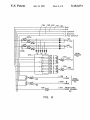
110b
top 2
up 3
top 4
top 5
top 6
P16. 68
Y Pos
top 1
116
120
1110
L middle
L rear
L key
R Key
R rear
R middle
R fwd
top 1
X Pos
top
top
top
tap
top
Vreg
Hand Force
8°
FIG. 6C
6
5
4
3
2
US. Patent
July 21, 1992
Sheet 5 of 8
5,132,671
Vreg
Gnd
B Common
A Common
X Pos Common
195
R Key \
196
L Key
FROM
>SENSOR
74
197
X Pos
198
Y Pos J
199
A
FORCE
200
FROM
SENSOR
72
FORCE
201
FIG. 9
FROM HAND
FORCE SENSOR
80
US. Patent
July 21, 1992
Sheet 8 of 8
INTEGRATED GRAPHICS
5,132,671
10,151
INPUT DEVICE
FIG. 12
I
GRAPHICS
PROCESSING
/\
240
UNIT
275
DISPLAY
\
FILE
EDIT
‘
OP'ITONS
WINDOW
PAINT
/
FONT
SIZE
STYLE
2800
A
y”/
1
5,132,671
2
INTEGRATING GRAPHICS INPUT DEVICE
device, gross and ?ne control of cursor position were
generated, respectively, by a moveable cover and a
moveable puck contained within the cover.
BACKGROUND OF THE INVENTION
The invention relates to graphics input devices which
are operated manually by a user to provide signals de
SUMMARY OF THE INVENTION
The invention is an apparatus for use in a graphics
?ning a graphical object whose image is to be displayed
processing system in which a graphics processor re
in a graphics system.
sponds to graphics input signals descriptive of a graph
In the prior art, hand-operated pointing or picking
devices are known. These devices are operated by a
user to position a cursor on the screen of a graphical
output device such as a display. The primary role of
these devices is to permit a user to select a speci?c XY
location on a display screen. Other devices, called loca~
ics object by operating a graphics output device to
display an image of the object. The apparatus provides
to the graphics processor graphics input signals descrip
tive of the graphics object. The apparatus includes a
manually operable ?nger grip assembly with a ?rst
pressure sensor for providing pressure-generated, force
tor devices, include the tablet, the mouse, the trackball,
vector signals representing a display location on the
and the joystick. All of these devices are employed to
graphics
output device. A pressure-responsive lockout
move a screen cursor, and operate in combination with
switch
assembly
generates a lockout' signal. The lockout
separate devices which input information relevant to
signal is for indicating inactivation of the force vector
the location occupied by the cursor. Most commonly,
function buttons, function switches, or alpha-numeric 20 signals. In the apparatus, a stylus assembly is moveable
in two dimensions and has a position sensor for generat
keyboards are used for command or information entry
after positioning of a cursor.
ing graphics input signals representing a multi-dimen
In the prior art, the drawing of graphic objects has
sional portion of a graphics object which is to be dis
played at the indicated display location. An interface is
been the province of a program entered into a graphics
processor. Commonly, such an application program 25 connected to the ?nger grip assembly, to the lockout
utilizes a bottom-up procedure for object creation,
using hierarchially-arranged object components. The
switch assembly, and to the stylus assembly for receiv
ing the force vector signals, the lockout signal and the
graphics input signals. Last, a processor communicator
components map to a set of output primitives with mas
ter coordinates which are used to control the function
connected to the interface means communicates to the
30
of an output device, such as a display.
graphics processor display location signals representing
Free-hand creation of graphical objects by a user
currently is supported by complicated devices having
large drawing surfaces upon which the user moves a
stylus or pen to draw an image. The drawing surface is
related to the display surface by a dedicated applica
tions process which maps the drawing surface to the
display area. When the drawing is being made on the
drawing surface, a conversion function is invoked, dis
patching the application program, and converting the
drawing into an image which is displayed on the screen
of the display device.
The invention has the objective of providing a user
with a graphics input device which permits the display
an updated position for the location in response to the
force vector signals received by the interface, the lock
out signal, and graphic input signals representing the
graphic object to be displayed in the updated position.
The principal object of this invention is to provide a
graphics input device which integrates graphics input
position information and graphics object information
which is to be input at the indicated position.
It is the further object of this invention to provide
repositioning control of a position area displayed by a
graphics processor.
A further objective is to also provide graphics object
device of a graphics processing system to be used like a
input signals de?ning a portion of an image which is to
drawing surface, without the need to provide a physical 45 be displayed in the position area.
surface as an analog to the display surface. This permits
Other objectives and attendant advantages of this
a graphics processor system to provide to a user imme
invention will become manifest when the following
diate feedback, or echoing, of a drawing operation
detailed description is read with reference to the below
which the user is conducting. Thus, the display screen
described drawings.
of a CRT may be used much as a blank tablet upon 50
BRIEF DESCRIPTION OF THE DRAWINGS
which a user can draw.
The integrating graphics input device which has been
invented by the applicants provides hand-to-eye feed
back through a graphics processor system by combining
cursor-like movement of a position area on a display 55
surface, together with tablet-like entry of graphical
image information by means of a stylus which can be
manipulated by the user to draw within the located
positioned area. The device can be used to enter a con
tinuous image by successively relocating the position
area in a sequence of overlapping positions within
which the user's manual input is integrated to form a
continuous, coherent image.
The closest prior art to this device is the inventor's
FIG. 1 is an isometric perspective view of the inte
grating graphics input device.
FIG. 2 is a side-view of the device illustrated in FIG.
1.
FIG. 3 is an exploded assembly diagram of the device
of FIG. 1.
FIG. 4 is an elevational side sectional view of the
device of FIG. 1, the view being taken along line 175 of
FIG. 3.
FIG. 5 is a magni?ed, side sectional view of a stylus
slider in the device of FIG. 1.
FIGS. 6A, 6B, and 6C illustrate the sensors used to
integrating pointing device, described in US. Pat. No. 65 provide graphics object force vector, and lockout sig
nals in the device of FIG. 1.
4,719,455 which is incorporated herein by reference. In
that device, graphical input was provided by a hand
FIG. 7 is a top plan view illustrating a circuit board
manipulated device which ?t to the user's hand. In the
included in the assembly of the device of FIG. 1.
3
5,132,671
FIG. 8 is a top plan view illustrating the orientation
of certain assembly components with respect to the
circuit board.
FIG. 9 is a circuit schematic diagram illustrating the
4
42 and 43, respectively, and are held therein by retainers
24 and 31.
With the carriage 20 aligned, by way of the slots 42
electrical operation of the invention in generating posi
tion and graphics object input signals to be input to a
and 43 with the case top 40, and held to it by the retain
ers 24 and 31, the opening 20 is aligned with an oval
opening 41 in the case top 40. The tip 15 of the stylus 14
graphics processor.
extends through the oval opening 41.
FIG. 10 is a block diagram illustrating the inter-con
nection of the device with a graphics processor.
upper portion of the ?nger grip 12. The ?nger grip 12 is
FIG. 11 is a detailed schematic diagram illustrating an
analog to digital converter of FIG. 10.
FIG. 12 illustrates the response of the graphics pro
cessor of FIG. 10 to the signals input by the device of
FIG. 1.
DETAILED DESCRIPTION OF THE
PREFERRED EMBODIMENT
A circular opening 45 in the case top receives the
retained against the case top 40 by a grip retainer 50.
The annular extension 12a of the ?nger grip 12 has a
larger radius than the hole 45, and is sandwiched be
tween the case top 40 and the retainer 50. The retainer
is attached to the case top 40 by screws 53 which are
received in threaded bosses 54. The bosses are formed
as part of the case top 40; however, for clarity, they are
shown detached from the top. A disk lever 52 engages
a recess in the shaft of the ?nger grip 12 and is posi
The integrating graphics input device of the inven
tioned between the ?nger grip 12 and the circuit board
tion is illustrated in external perspective in FIG. 1 and in
a slightly magni?ed side elevation of FIG. 2. The de 20 70 by a pivot 56 with an annular extension, which ?ts
vice is indicated by reference numeral 10 and includes a
through a hole 71 in the circuit board. An anchor 57
extends through the bottom of the pivot 56 and contacts
case 11 in which is mounted a ?nger grip 12, a stylus
like pen 14, and function keys 16 and 17.
the bottom of the disk lever 52, and is retained there by
The device 10 is a stationary apparatus which a user
. a threaded screw 58 which is screwed into a threaded
manipulates by hand to enter position and graphics 25 recess in the center of the disk lever 52.
The pen 14 is retained in an elongate slide 63 which is
objects information in the form of hand force and posi
clamped pivotally between the grip retainer 50 and the
tion signals, respectively, into a graphics processor for
display. In use, the user grasps the ?nger grip 12 to
change the location of a position area on a graphics
processor display. The grip 12 is operated like a station
ary joystick to support cursor-like repositioning of the
case top 40 by one of the threaded screws 53. The tip 15
of the stylus 14 is received in a tip retention recess 67 in
the top portion of a rounded slider 66 having two coax
ial ?anges which slidably engage respective faces of the
display area.
slotted elongate slide 63. The slider 66 is free to slide in
When the position area is relocated as just described,
the slot 64 while the pen tip 15 is engaged in the recess
the user grasps the pen 14 and manipulates it in the X
67.
and Y directions to draw in the position area. The pen 35
The circuit board 70 has a force sensor 72 in the form
14 is free to move in two dimensions, its movements
of a force sensing resistor upon which the lower edge of
the rim of the disk lever 52 rests. Forward of the sensor
being translated, by means described below, into graph
ics object input signals which are used by a graphics
72 is a ramped surface 75 on which is held a position
processor to display the trace of the pen‘s path in the
sensor 74. A hand pressure sensor 80 is positioned on
display area. The pen 14 also permits the operator to 40 the bottom of the circuit board 70 and contacted bv a
enter Z-axis information by varying pressure on the pen
button 81 on a threaded foot 82.
14. The result, for example, would be to vary the width
The components 80, 81, and 82 form a lockout switch
or density ofa line being drawn.
whose function is discussed below. All of the sensors
are attached by adhesive means to the circuit board 70. The function keys 16 and 17 provide conventional,
programmable functions which are selected by the user 45
The tip ofthe round slider 66 is illustrated in a magni
depressing one or the other of the keys.
The construction details of the device 10 are illus
trated in FIGS. 3 and 4. As shown in the Figures, the
case 11 is assembled from a carriage 20, which ?ts to a
?ed cross-section in FIG. 5. FIG. 5 illustrates the con
nection of the stylus 14 to the slider 66. The stylus is
connected to the slider bv a spring 89, one end of which
receives the tip 15 of the stylus. The spring 89 allows
case top 40. The case top 40 is attached to the case 50 the user to hold the stylus at any desired angle. The
bottom 46; a circuit board 70 is positioned between the
case top and the case bottom and attached to the case
bottom.
round slider 66 is a hollow cylinder in which the other
end of the spring 89 is retained in the tip retention recess
67. The spring 89 has a ?anged tip extension 90 which is
in bayonet engagement with a slider plug 94. The slider
boot 19 having a rim 19a. The boot 19 is inserted into a 55 plug 94 is moveably held within the slider, so that it can
circular opening 21 in the carriage 20, with the rim 19a
rotate, allowing the user to turn the attached stylus 14
engaged in an annular groove 21a of the carriage open
to any desired orientation, and it can also move up and
ing. The keys 16 and 17 are mounted to the carriage 20,
down, in response to upward pressure by a spring 95
with the right-hand key 16 received in a quadrilateral
and varying downward pressure by the user on stylus
recess 22 having a hole 23. The key 16 includes a rod 60 14. As shown, the plug 94 is bored out to contain the tip
160 which ?ts through the hole 23 and a stylus 25. Simi
15 in an upper bore, as well as a tip 96 which is spring
larly, the left-hand key 17 has a key rod 170 and is
loaded by the spring 95 in a lower bore. The tip 96
received in a quadrilateral recess 27 of the carriage. The
includes a rod which can project into the upper bore of
key rod 170 extends through a hole 28 and rod guide 29.
the slider plug 94. The upper end of the tip 96 contacts
The bottom of the rod 170 ?ts into the stylus 30.
the lower end of the tip 15 when the spring 95 is com
As thus described, the keys are held to the carriage 20
pressed by the user pressing down on the stylus 14.
by engagement of the tips of the rod 160 and 17a in the
When this happens, there is a direct transfer of force
styli 25 and 30. The styli 25 and 30 are received in slots
from the stylus 14 to the tip 96, as shown in FIG. 5.
The stylus 14 includes a tip 15 which ?ts through a
5
5,132,671
FIG. 5 illustrates partial compression of the spring 89
when the tip 15 is pressed with moderate force down
wardly toward the slider 66. As illustrated in FIGS. 4
and 5, the pivot of slide 63, together with the slider 66
which moves in the slot 64, enables the tip 96 to move
under the force of the pen 14 over the position sensor
74. When assembled, the tip 96 rests on the position
sensor. Movement of the pen 14 moves the tip 96 upon
the sensor 74, with more or less pressure according to
6
tion signals which, taken together, correspond to the
two dimensional position of the pen 14 with respect to
the sensor 74. The second position signal is the Y Pos
signal taken from the corresponding tap of the sheet
11Gb. Together, these signals precisely de?ne the instan
taneous location of the pen; a continuous signal chro~
nology of these two taps therefor corresponds to an
object drawn on the sensor 74 by the pen.
The regulated voltage vreg is brought also to the taps
the force exerted against the tip of the pen by the user.
R Key and L Key to energize the conductive traces on
Even with no pressure exerted bv the user in the stylus,
the right and left-hand edges, respectively, of the sheets
the spring 95 maintains the tip 96 against the sensor 74
with enough force to track the position of the stylus.
110a and 11Gb. Each of these conductive trace patterns
is aligned with a corresponding conductive pattern on a
facing surface of the other of the two sheets. When the
sheets are assembled as in FIG. 7, the right-hand con
ductive patterns afford sensor arrangements to detect
depression of one of a key. For example, with the as
The position sensor 74 is illustrated unassembled in
FIG. 6A and 6B. As shown, sensor FSR 74 consists of
two thin, rigid, plastic sheets 110a and 110b, each carry
ing a pattern of printed conductive traces and a variable
resistance compound. The sheets are identical images,
and form the sensor 74 by being assembled with an
sembly shown in FIGS. 2 and 7, the righthand key 16
is positioned above the conductive trace 120. When the
key is depressed, the trace pattern 120 is brought into
insulating sheet between them. When assembled, oppo
site sides of the sheets 110a and 11Gb face upward. The
contact with the conductive block 121, with the result a
assembled sensor 74 is illustrated in FIG. 7. As FIG. 7
voltage is provided on the tap R middle.
illustrates, the sheet 110a overlays the sheet 1101), with
the center, insulating sheet not illustrated.
The operation of the sensor 74 will now be explained
with reference to the sheet 1100. with the understanding
that the sheet 11Gb operates in the same manner. In
operation, a regulated DC voltage, Vmg, is fed to tap 5
of the sheet, while DC ground is fed to tap 2 of the
sheet. The resistive compound forms a L-shaped ?gure
along the left and bottom margins of the array of con
The hand force sensor of the lockout switch is illus
trated in FIG. 6C and operates in the same manner as
the function key sensors. In this regard, refer also to
FIG. 4, where the hand-force sensor 80 is shown posi
tioned on the bottom, rear of the circuit board 70 di
rectly over the button 81. In this position, whenever the
user applies pressure on the rear portion of the case top
40, the pressure is transferred through the connecting
structure of the case 10 to the case bottom and to the
ductive traces 1110. A continuous voltage drop is in
duced between 1130 where tap 5 intersects the resistive
compound and 1120 where tap 2 intersects the resistive
compound. Thus, at any of the conductive traces which 35
attached circuit board, which causes the hand force
sensor 80 to press against the button 81. When this
occurs, voltage Vmg is conducted to the Hand Force tap
intersect the L-shaped resistive pattern between 1130
In FIG. 7, the translational pressure sensor 72 is illus
trated. As with the position sensor 74, the translational
and 1120. a distinct voltage level can be measured
which lies between V,eg and ground. Such a voltage
provides a positional signal corresponding to a point
where pressure is applied in the array 111a. For exam
ple, consider that the tip 96 contacts the array 111:: at
114. and the user applies a force directed onto the sensor
74 at 114. At 114, the composition of the center insulat
ing sheet causes that sheet to become conductive in
of the sensor 80.
pressure sensor 72 comprises two sheets with a pattern
of conducting traces and a variable resistance pattern.
However, on each sheet, the overall pattern is semi-cir
cular. In FIG. 7, only the conductive and variable resis
tance patterns of the top sheet 150 are visible, it being
understood that the bottom sheet a has similar semi-cir
cular conductive/resistive pattern which is rotated 180°
response to pressure applied by the stylus in the inter 45 with respect to the pattern on the sheet 150 to form a
stice at 114 between conductive traces 115 and 116. The
complete circular pattern. These sheets are also assem
trace 115 intersects the L-shaped resistor at a point
bled on either side of a center insulating sheet (not
indicated by a respective voltage on the trace 115. Con
shown) which becomes conductive in response to appli
ductivity in the insulating layer at 114 causes current to
cation of pressure. On the sheets 150 and 152, VNg is fed
?ow between the trace 115 and the trace 116, thereby 50 to one of the two taps which connect to the semi-circu
bringing the trace 116 to the potential of 115. The con
lar resistive trace, such as the trace 153, while the other
ductive trace 116 is one of a plurality of conductive
tap is connected to ground. This provides a continuous
traces which alternate with the traces connected to the
voltage drop between vrgg and ground from one end of
L-shaped resistor. These alternating traces are con
the semi-circular arc to the other. The center tap, tap
nected in common to a trace 117 which is brought out
155 in the sheet 150 and tap 157 in the sheet 152 provide
a voltage corresponding to the location on the continu
to a tap labeled “X Pos" (for “X position"). In response
ous resistive circle formed by the two opposing semi
to the pressure at 114, the voltage induced on the trace
circular conductive patterns on the sheet 150 and 152.
116 is brought out to the X Pos tap; therefore, the volt
age level at this tap conveys precisely the location of
Pressure on the ?nger grip 12 is transferred to one or
the other of the sheets of the sensor 72 through the disc
the tip 96 when pressure is applied to the pen 14. Fur
ther, the amount of current which flows between the
lever 52. A radial A or B Force signal is generated at tap
conductive strips 115 and 116 is directly related to the
155 or tap 157 when the material of the center insulating
amount of force exerted at 114 by the tip 96. Therefore,
layer becomes conductive in response to the hand grip
the current at the tap X Pos indicates the amount of
pressure. The A or B Force signal indicates position
65 along one of the two semicircular patterns and gives
pressure on the pen.
Since the sheets 110a and 11% are stacked, with a
pressure at that point. These two components, of
separating insulating layer which operates as described
course, define a vector whose function is described
above, they operate similarly to produce a pair of posi
below.
7
5,132,671
The sensors 72 and 74 are attached to the circuit
8
ward. In the rear position, the carriage 20 is closest to
board 70 as illustrated in FIG. 7. Signal connection
the ?nger grip 12, and the function keys 16 and 17 are
between the sensors and the outside of the device 10 are
positioned over the lower most conductive traces'on
by a wiring harness 160. The harness includes individual
conductors connected, by conventional solderboard
means, to the taps of the sensors 72, 74 and 80. In this
manner, VREG, common, and ground potentials are
connected into the device 10, while the X and Y POS,
Right and Left key, I'Iand Force, and A and B Force
signals are conducted from the sensors 72, 74, and 80
out of the device 10.
Referring back to FIG. 1, in the best mode of this
invention, conversion and interface electronics are lo
the sensor 74. In this position, key signals will be
brought out on the tap labeled “R Rear" and “L Rear".
When moved to the middle position, the R and L Mid
dle taps provide the function key signals. When the
carriage is slid to the position furthest from the ?nger
grip 12, key signals are provided on the R and L FWD
taps. In the rear position, ground is provided to tap 3 of
both of the conductive sensor portions 110a and 11%.
In this position, V"; is provided to tap 4. In the middle
position, tap 5 of both sheets is connected to vrgg while
tap 2 of both sheets is grounded. Last, in the forward
cated in an apparatus enclosure 161 and connected to
the electronic components of the device 10 by means of 15 position, tap 1 is grounded, while tap 4 receives Vmg.
the wire harness 160. The wire harness 160 penetrates
As FIG. 8 shows, recon?guration of tap voltage con
the device 10 through the case bottom 46 bv way of an
nections selects the portion of the conductive traces of
aperture 47 (FIG. 3). It should be evident, and it is
the sensor 74 which will be positioned under the circu
contemplated by the inventors, that all of the circuit ' lar opening 21 de?ning the drawing area of the pen 14.
functions to be described next can be integrated into 20 Although not illustrated in the drawings, conventional
monolithic IC form and mounted inside the device 10.
mechanical means are used to lock the carriage 20 in a
Refer now to FIG. 8 for an understanding of the
selected position.
_
spatial relationships between the pen assembly and the
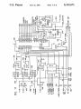
Refer now to FIGS. 9, 10, and 11 for an understand
sensor 74, and the ?nger grip and the sensor 72 As
ing of the signal conversion and interface circuitry ob
shown in FIG. 8, when the device 10 is assembled, the 25 tained in the electronics enclosure 161 (FIG. 1). FIG. 9
circular opening 21 in the carriage 20 is centered in the
oval opening 41 of the case top 40. The pivotal connec
tion ofthe elongate slide 63 and the sliding arrangement
between that slide and the round slider 66 permit the tip
96 to be moved by movement of the pen anywhere
within the circle de?ned by the circular opening 21. As
FIG. 8 illustrates, this circle is centered in the conduc
is a schematic diagram which recapitulates the signal
path layout discussed above in connection with FIGS.
6A, 6B, 6C, and 7. The Vmg, common, and ground
signals are generated by conventional means, not illus
trated, and conducted initially on signal lines 190 and‘
191, respectively. These lines connect directly to the
sensors 72 and 80, and are connected to the sensor 74 by
tive trace arrays of the sheets making up the sensor 74.
way of a 4-pole, 3-position switch 218. Common signals
In operation, the pen 14 can be moved by the user to
are brought into the sensor 72 for A and B Force sig
draw any kind of a ?gure within the circle 170, with the 35 nals, respectively, on respective signal lines 192 and 193.
time history of the image being available from the X Pos
An X position common signal is conducted on signal
and Y Pos taps on the sensor 74.
line 194 to the switch 218 for provision to the sensor 74.
The switch 218 is connected to the taps on the sheets
comprising the sensor 74 as illustrated. Signal lines 195
The ?nger grip 12 is aligned with the sensor 72 such
that the ?nger grip assembly, including the disk lever
52, is coaxial with the circular conductivity pattern on
sensor 74. As illustrated in FIG. 8, the radius de?ned by
the edge ofthe disk lever 52 is less than the radius to the
circular resistive pattern on the sensor 72. In operation,
the ?nger grip is grasped by the user and force is ex
and 196, respectively, conduct signals from the sensor
74 to indicate activation of the right or left keys 16 and
17, respectively. Signal lines 197 and 198 conduct X and
Y position signals from the sensor 74. Signal lines 199
and 200 conduct the A and B Force signals from the
erted on it with a component which is radial to the 45 sensor 72, while signal line 201 conducts the Hand
circular conductive pattern of the sensor 72. The radial
Force signal from the sensor 80. When the carriage 20 is
vector of the force is indicated bv the A or B Force
in the forward position, the right and left key 16 and 17
signal generated by the sensor 72 in response to the
are depressed, causing the conductive patterns 203a and
pressure. Thus, if the pressure exerted on the ?nger grip
203b in the sensor 74 to conduct, thereby providing a
12 is toward NNE in FIG. 8, an A Force signal of a
voltage on the right and left key signal lines 195 and
particular voltage and current will be generated by the
196. In addition, corresponding signals are diode-con
FSR 72 through the tap 155. The magnitude of the
nected to the switch 218 to con?gure it such that vng
voltage is directly related to the direction of the vector,
on signal line 190 is connected to the tap 4 connections
and, therefore, to the direction of the pressure applied
of the sensor 74, while ground is connected to tap 1 on
to the grip 12. The current is related to the magnitude of 55 sheet l10b and the X common signal to tap 1 on the
the pressure.
sheet 110a.
Refer now to FIGS. 1, 3, and 8 for an understanding
At the middle position, activation of the function
of how the device 10 can be adjusted for the conve
keys connects Vrex to tap 5 of both sheets of the sensor
nience of the user by sliding the carriage 20 either
74, ground to tap 2 of sheet 110b, and X common to tap
toward or away from the ?nger grip 12 along the line 60 of sheet 11011 Last, in the rear position, the function
175 in FIG. 3. The adjustability is provided to accom
keys operate the switch 218 to connect Vmg to tap 6 on
modate varying hand dimensions, thereby contributing . sheets 110a and 11012, ground to tap 3 of sheet 11%. and
to the comfort of the user. The carriage 20 slidably
X common to tap 3 of sheet 1100. The sensors 72, 74 and
engages the case top 40 and can be slid with respect
125 operate as described above to provide the Hand
thereto by virtue of the engagement of the case top 40 65 Force, A and B, and X and Y position signals on signal
between the carriage 20 and the retainers 34 and 31
lines 201, 200, 199, 198, and 197, respectively.
attached to the bottoms of the function key rods 16a and
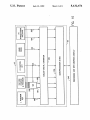
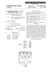
FIG. 10 illustrates the means for integrating the inte
170. Three positions are possible: rear, middle, and for
grating graphics input device 10 with a graphics display
5,132,671
processor. In FIG. 10, the graphics display processor
includes a processing unit with a graphics display 240
which interfaces with the electronics unit 161. The
interface between the electronics unit and the device 10
has already been explained above with reference to
FIGS. 6A-6C and 9. The primary components in the
electronics unit 161 include a circuit 250 for analog-to
digital conversion (ADC) and a microprocessor 255.
Essentially, the ADC 250 receives and converts the
level signals described above to digital signals, formats
the digital signals and provides them to the micro
processor 255. The microporcessor 255 receives the
formatted digital signals and conducts a communication
process with the processing unit 240 for transfer of
those signals to the processing unit for incorporation
into a graphics processing application.
Refer now to FIG. 11 for a more detailed illustration
10
the A buffer is con?gured to sense position (voltage),
the buffer (not shown) which corresponds to buffer 262
is connected to pin 12; when the A buffer senses pres- .
sure (current), the buffer (not shown) corresponding to
buffer 263 is connected to I2.
The ADC 260 receives a divided clock by way of a
conventionally-con?gured ?ip-?op 271, reference volt
age signals from ground and from the generator 261,
and control signals from the microprocessor 255 to
conventionally convert the level signals present at its
input (I) pins to digital words representative of the
converted levels at the output (D) pins. The output (D)
pins of the ADC 260 are connected to an address
/databus which shares, with the output pins, common
connections with three address (A) pins of the ADC
260. In operation, the microprocessor 255 convention
ally controls the ADC with FETCI-I_DATA, CON
VERT, LOAD_ADDR, and RESET control signals.
of the ADC circuit 250. In FIG. 11, the signal paths
194-199 all correspond to identically-numbered signal
These signals are conventional and operate the ADC
paths in FIG. 9. All of these signals are fed to respective 20 260 to sequentially address input pins, sample the volt
input ports of a conventional analog-to-digital con
age at the currently-addressed input pin, and output a
verter (ADC) 260. The converter receives a reference
digital word corresponding to the level of the voltage
voltage for conversion from a reference voltage circuit
sampled at the currently-addressed input pin. The ad
261. In addition, the ADC 260 receives the X position
dress is then changed to the next input pin, and so on. In
signal through a buffer 262, the pen force signal through
synchronism with the sampling sequence, the micro»
a buffer 263, and the Y position signal through a buffer
processor 255 con?gures the switches 266, 267, and 268
264. The buffers 262 and 263 are both connected,
to ensure that, for example, when pin 10 is addressed,
through respective switches 266 and 267 to the signal
the X Pos voltage signal is buffered through the buffer
line 197, which is also connected to a switch 268. The
262. Similarly, when the input pin 11 is addressed, the
signal line 194 is also connected to the switch 268. The 30 switches 266, 267, and 268 are con?gured to provide the
switches 266, 267, and 268 are con?gured by respective
pen pressure current through the current buffer 263.
control signals XPOS, XFORCE, and XSEL which are
Further, when A or B FORCE signals are being
provided from the microprocessor 255. These signals
sensed, the ADC 260 is similarly addressed and con
are conventional control signals which condition the
trolled, in synchronism with the multiplexing of the
switches 266, 267 and 268 to on or off conditions. These
circuit 272, to sample and convert A position and A
signals are provided to multiplex the X Pos signals on
signal line 197 to provide both X position information
relating to the X position of the pen with respect to the
sensor 74, and also to provide the pen pressure signal.
For the X position signal, the switches 267 and 268 are
force magnitude signals through pin I2, and B position
and B force magnitude signals through pin I3.
conditioned to their OFF states, while the switch 266 is
conditioned ON. In this case, the X Pos signal is fed to
the buffer 262 for buffering to the ADC 260. In this
state, X Pos Common line 194 is grounded to provide a
Refer now to FIG. 11 and to Tables l-IV for an
understanding of how the operation of the ADC 260 is
controlled to convert the signals produced by the FSR’s
72, 74, and 80. In Table I, a series of functions and
global variables are de?ned. Then, in a main loop, the
converter 260 is interrogated in a sequence of calls to 3
subroutines: ADCSTB, ADCSTAT, and ADCDATA
reference for the X Pos signal. Next, the control signals 45 (Tables II, III, and IV, respectively).
condition the switches 267 and 268 ON and turn OFF
Interwoven with the call sequence of Table I is a
the switch 266. In this state, the resistor R3 converts the
control sequence for conditioning the three switches
current input on the signal lead 197 to a voltage signal
266, 267 and 268 for reading either X Pos or the pen
proportional to the current level, and thus, to the force
downforce signal output by the sensor 74. The control
with which the pen 14 contacts the FSR 74. This signal 50 sequence also conditions the A/B POS, -FORCE, and
is buffered to the ADC 260 through the buffer 263.
-SEL signals to read A position, A magnitude, B posi
The Y Pos signal on signal line 198 is fed continu
ously through the buffer 264 to the ADC 260. The
Hand Force signals and the left and right key signals are
fed directly, without buffering, to the ADC 260.
The A and B FORCE signals are buffered and multi
plexed in a circuit 272. The circuit 272 includes respec
tive buffering sections for the A and B FORCE signals
which operate as described above for the X Pos signal
tion, and B magnitude signals output by the sensor 72.
Initially, a main loop is de?ned in step 116, conditions
are initialized in steps 117-119, and in step 120, the
XPOS, APOS and BPOS signals are energized. Activa
tion of XPOS to turn ON the switch 266. Concurrently,
the switch 268 is OFF grounding the XPOS Common
line 194, which provides a ground potential against
which the X position information is measured by the
to obtain both position and magnitude signals which 60 buffer 263. The control signals are hexadecimal (H)
correspond to the position of the grip 12 with respect to
signals which are output through microprocessor port
the sensor 72 and to the pressure with which the grip
58H. The A and B POS signals similarly con?gure the
contacts the sensor. The buffers operate in response to
buffer sections of circuit 272.
the ground, A and B common (COMM), and A/B POS,
Next, a loop index (i) is de?ned, initialized to zero,
A/B FORCE, and A/B SEL signals a do the buffers 65 limited to the range of whole numbers between 0 and 10
262 and 263. In addition, the A/B SEL signals operate
and incremented by 1 for each step of a looped sequence
to multiplex the outputs of the A and B buffers to input
beginning at line 124 of Table I. A byte-wide Ill-posi
pins 12 and 13 of the ADC 260. Thus, for example, when
tion buffer is initialized in step 124 and then an endless
11
5,132,671
loop entered in steps 125 and 126. In steps 127-130, the
X position of the pen 14 is obtained by conversion of the
X Pos signal on the path 267, 263, 260 in FIG. 11. First,
the ADCSTB macro (Table II) is called. This macro
provides an address (ADDRESS 0 in line 128) on the
address databus connected to the ADC 260, a LOAD].
JADDR control signal to the connected to the ADC
260, a ADC 260 notifying it to load the address on the
address/databus, and then a CONVERT (ADC
12
is set, Table I executes the TESTXMIT subroutine. The
TESTXMIT subroutine polls the host graphics process
ing unit 240 for a communications initiation handshake
signal. When it detects a "start" handshake signal from
the host, it transmits l0 bytes of data by transferring the
contents of the 10-position buffer which is loaded as
described above to a transmit buffer (XMITBUF).
Transmission is based upon availability of the transmit
buffer, which is determined by availability of a serial
STROBE) control signal commanding the ADC 260 to
I/O channel. The availability is tested in steps 183 and
begin its procedure of converting the level of the signal
185. If available, the subroutine SENDSTR is invoked
on the input port addressed on the address/databus. The
to transmit a string of 10 bytes from the transmitbuffer
addressed input port is 10, connected to the buffer 262.
through a serial I/O port to the graphics processing unit
Therefore, the X Pos signal is converted to digital for
240.
mat by the ADC 260.
15
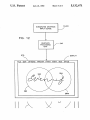
The reaction of the graphics processing unit 240 to
The ADC 260 operates conventionally to provide an
the position, hand force and function key signals gener
end of conversion (EOC signal) which sets a status
ated by the device 10 and converted through electron
?ip-?op 270. This conditions an ADC13STATUS signal
ics 161 is illustrated in FIG. 12.
to an When the ADC_STATUS signal is conditioned
As FIG. 12 illustrates, the graphics processing unit
ON, the ADC DATA macro (Table IV) is dispatched,
20 240 operates a conventional display 275 which may
which reads the converted data off of the address
/databus, and resets the status ?ip-?op 270 via the
RESET signal. The data which is converted from the
comprise a CRT. The graphics processing unit 240
includes a dispatchable graphic input device handler
(not shown) which receives the converted signals from
signal input at ADC I0 is entered into location {0} in
the electronics 161, and passes them to a graphics pro
the buffer.
25 cessor (now shown) for driving a display. The user of
Following conversion and buffering of the X PPS
the device 10 is enabled by the graphics processing unit
signal, a hexidecimal code '80’ is provided through
240 to observe a drawing being made on the display 275
processor port 58H, which turns OFF switch 266, while
by means of the input device 10. In this regard, the
turning 268 ON. This “?oats" the signal line 174, while
graphics processing unit 240 provides a defined position
pulling down the signal line 197 through the parallel 30 area showing the user where, on the image being dis
resistances R2 and R3.
played, the drawing input from use of the pen is being
Next, in steps 135-143, the A and B position s are
entered. In FIG. 12, this area is displayed as a circle 280,
sampled in the same manner as the X position signal,
corresponding to the circle 21 (FIG. 3) within which
and placed in buffer locations 3 and 4. The ASEL and
the pen 14 is constrained to move. The circle 280 is
BSEL signals are not active, which appropriately con 35 repositioned on the display by use of the hand grip 12,
nects the buffered versions of the position signals to the
unless the Hand Force sensor 80 signal is activated by
ADC 260 through the multiplexing section of the cir
pressure on the case top. When the user wishes to repo
cuit 272. Then, in step 144, the APOS and BPOS signals
sition the position circle 280, the user reduces pressure
are deactivated while the ASEL and BSEI. signals are
from the back of the case 11, thereby reducing the cur
activated.
rent on the hand force sensor 80 resulting from pressure
Then, in steps 145-148, the Y position buffer 264 is
against the button 81 on the rear bottom of the device
addressed via the ADC 260, the Y position signal is
(FIG. 4). This signals to the processing unit 240 that the
converted and sent to buffer location 1. The A and B
position circle 280 allowing it to be moved (“dragged”)
FORCE signals are activated in step 149. Next, in steps
on the screen of the display 275 in a direction corre
150-153, the Hand Force signal on signal line 199 is 45 sponding to the A or B Force signal derived from the
convened and placed in buffer location 5.
sensor 72. The circle 280 is moved in the direction cor
By the time the program in Table I reaches steps
responding to the active A or B position and at a rate
150-153, the switches 266, 267, and 268 have been
corresponding to the A or B force signal until horizon
turned OFF, ON, and ON, respectively, in enough time
tal pressure on the ?nger grip 12 is released. The posi
to damp out any switch bounce. Now, in steps 154-157, 50 tion circle 280 is then kept at the last updated X-Y
the pen downforce signal is provided through the buffer
position. In FIG. 12, the updated X-Y position is indi
263, converted, and stored in buffer location 2. In pro
cated by 2800.
gram line 158, all of the switches 266, 267, and 268 are
While positioned on the display 275, the position
turned OFF, while the ASEL, BSEL, A FORCE, and i circle 280 de?nes an aperture into the image being
B FORCE signals are activated. Then, A FORCE, B 55 drawn on the display through which the user can enter
FORCE and left button signals are converted in steps
X and Y position signals, together with pen force sig
159-171. In step 171a. the XPOS signal is activated
nals, to create a graphics object for display on the
together with the APOS and BPOS signals, turning ON
screen. This is illustrated in FIG. 12, where the scripted
the switch 266, and preparing the buffer 262 for X Pos,
word “Even" 283 has been entered into the image on
A Pos, and B Pos conversion. Following this, the right
the display 275 by use of the pen 14 while the position
button status is converted and stored in buffer location
circle is in the position indicated by 280. The word 283
7 in program steps 172-176. The program loops, at step
represents the trace of the tip of the pen 14. This trace
177 back to step 125.
is provided by continuous transmission of X and Y POS
Reference is now made to lines 129, 138, 142, 150,
signals to the graphics processor as described above.
154, 162, 166, and 174 of Table I, all of which call a 65 The width, or density, of the graphics object 283 which
TESTXMIT subroutine. The TESTXMIT subroutine
traces the path of the pen tip is given by the sequence of
is called and executed while the ADC is conducting a
hand down force signals transmitted with the X and Y
conversion process. Thus, until the ADC_STATUS bit
position signals. Movement of the position circle 280a in
13
5,132,671
14
response to use of the grip repositions the aperture in
TABLE l-continued
the displayed image. In the repositioned position circle,
/' X axis pen position '/
the scripted word "if" has been entered into the image.
Thus, by moving the position circle 280 in a particu
lar sequence of overlapping location, the user of the
device 10 can selectively create a graphics object using
127
128
129
130
Bi
135
136
137
I38
I39
the graphics processing unit 240, and enjoy instanta
neous visual feedback of the object during the process
of creation.
The design of the device 70 is intended to position the
stylus 14 and grip 12 so that they can be enclosed in the
span of a user's hand and operated simultaneously. This
adcstb(0);
/'start conversion '/
while (adcstat (0))
/'wait till conversion done '/
testxmit( );
bul‘fer(0) = adcdata(0);
SCl5wil(OX84)l
/' A sensor position '/
/'start conversion '/
/'wait till conversion done '/
adcstb(2);
while (adcstat(2))
butTer(3) = adcdata(2);
/' B sensor position '/
/'start conversion '/
N0 adcstb(3);
while (adcstat(3))
permits simultaneous input of graphics signals and force
/'wait till conversion done '/
142 tesotmit( );
H3 buffer“) = adcdata(3);
signals to reposition the drawing area enclosed in the
position circle. When only graphics signals are to be
input, force signals are locked out by applying sufficient
/'set switches '/
144 setswit(0x88);
/' y axis pen position '/
hand force to the rear of the upper case to exceed a
/'start conversion '/
/°wait till conversion done '/
while (adcstat(l))
preset force. This can be applied by the rear of the hand
testxmit( );
being used to operate the stylus.
TABLE I
l'get adc data '/
/'set switches '/
20
_ /'set switches '/
/‘ hand downforce '/
60 ‘function of switch bits:
61 ‘80h = it select
62 ‘40h = it pos
63 ‘20h = x force
25
64 ‘10h : (not assigned)
65 ' 8h = a.b select
/'start conversion '/
/'wait till conversion done ‘/
158 setswit(OxOA);
/' ‘A‘ sensor force '/
‘ADC converter inputs:
7] ' 0 = x sensor position
l'set switches '/
/'start conversion ‘/
/'wait till conversion done '/
adcstb(2);
y sensor position
‘A' sensor pos/t'orce
‘8' sensor pos/force
hand force
while (adcstat(2))
testxtnit(- );
buiTer( 8) = adcdata(2);
it sensor force
35
left button
right button
/'start conversion '/
/'wait till conversion done'/
adcstb(3);
while (adcstat(3))
testxmit( );
bulTer(9) = adcdata(3);
80 'xmit order:
8| ' 0 = x pen pos
pen downi'orce
‘A‘ sensor position
‘B‘ sensor position
hand downl'orce
left button
setswit(0x00);
/'set switches '/
/' left key
adcstb(6);
while (adcstat(6))
/'star1 conversion '/
/'wait till conversion done '/
testxmit( )1
buffer(6) = adcdata(6);
/‘set switches '/
setswit(0x44);
/' right button '/
right button
39 ' 8
' 9
testxrnit( ):
buffer(5) = adcdata(4);
buiTer(2) = adcdala(5);
69 '
II
H
ll
II
while (adcstat(4))
testxmit( );
68 ' lh = (not assigned)
ll
II
/'start conversion '/
/‘wait till conversion done '/
adcstb(4);
154 adcstb(5):
while (adcstat(5))
67 ' 2h = a,b force
1
2
3
4
5
6
7
150
151
152
153
45
‘A' sensor force
‘8' sensor force
#de?ne void int
/'start conversion '/
/‘wait till conversion done '/
adcstb(7);
while (adcstat(7))
testitmit( );
bul't'er(7) = adcdata(7);
1
50
' - t'unction dei's —- '/
void init( );
void testxmit( );
void sendstr( ),
107 int getstat( );
int getchr( );
void settmr( );
unsigned int gettmr( ),
void adcstb( );
int adcstat( );
unsigned int ldcdata( );
void setswit( );
l'initialize SlO '/
l‘test request to itmit '/
static int i;
static char xmitbu? 10);
/'transmit result string'/
/‘!0 if char avail ‘/
/'char in lower byte '/
/‘set timer '/
/'get current timer value '/
l'start adc cycle '/
l'get adc status '/
l'get adc data ‘I
/'set control bits '/
l77 )
void testxmit( )
182 static char 'cp;
183 it' (!getstat( ))
55
l'oountcr °/
l'local buffer '/
/'pointer to chars '/
/'char not available? '/
184 return;
185 it‘ (getchr( ) != XON)
/'char not ‘start char’! '/
186 return
187 for (i = 0, i < 10, ++i) /Ixfer data to local buffer '/
188 xmitbut'(i)=buiTer(i);
189 sendstr(xmitbuf,8);
/’ -- global vars -—-'/
H5 static char bulTer (10)
/' value buffer '/
H6 main( )
[18 static int i;
H9 init(O.
120 setwit(0x44);
I23 for(i = 0;i < l0; ++i)
124 buiTetfi) = 0,
125 for (;;)
126 {
TABLE II
/‘counter '/
l'init SlOs '/
l'set switches '/
ADCSTB
65
: POP
b
;(RETURN ADDRESS)
POP
PUSH
PUSH
h
h
b
;CHANNEL NUMBER
;(RESTORE STACK)
MOV
OUT
OUT
a,l
;ADDRESS
ADCLD ;ADC ADDRESS LOAD
ADCCV ;ADC STROBE
5,132,671
15
0292
16
contacting the grip for generating a force vector signal
indicating said change in response to manipulation of
TABLE Il-continued
RET
the grip.
4. A graphics input device of claim 1, further includ
ing conversion means connected to the XY position
signal generator and to XY force vector signal genera
TABLE Ill
ASCSTAT
:IN
AN]
MOV
MVI
RET
ADCST
:GET SONAR STATUS
UJOOtXXJlB
La
;ADC ONLY
;RETURN STATUS
tor for converting the graphics entry signals and the
force vector signal to digital signals.
5. The graphics input device of claim 4 further in
cluding communication formatting means connected to
the conversion means for interprocessor communica
h,0
tion of the digital signals.
6. The graphics input device of claim 4, wherein the
TABLE IV
ADCDATA
:lN
MOV
MVl
RET
END
ADCDA
LA
PLO
;GET DATA
;RETURN DATA
conversion means includes an analog-to-digital con
verter separate from the case assembly and means con
nected to the XY position signal generator, to the XY
force vector signal generator and to the analog-to-digi
START
While we have described several preferred embodi
ments of our integrating graphics input device, it should
be understood that modi?cations and adapations thereof
tal converter for conducting the graphics input signals
20 and force vector signal to the analog-to-digital con
verter.
7. The graphics input device of claim 1, wherein the
XY
positioning assembly includes means for slidably
protection afforded our invention should only be lim
positioning
the stylus on the case assembly with respect
ited in accordance with the scope of the following
to
the
grip.
25
claims.
8. The graphics input device of claim 1, further in
1 claim:
_
will occur to persons skilled in the art. Therefore, the
I. A graphics input device, comprising:
a case assembly;
a penlike stylus;
a graphics entry area mounted to the case assembly; 30
an XY positioning assembly mounted to the case
assembly for moveably positioning the stylus on
cluding:
means for slidably positioning the carriage assembly
on the case assembly with respect to the grip; and
means for electrically positioning the graphics entry
area with respect to the carriage assembly in re
sponse to said positioning of the carriage assembly.
9. The graphics input device of claim 1, further in
the case assembly with respect to the graphics
cluding function keys mounted on the carriage assem
entry area;
an XY position signal generator mounted to the case 35 bly.
assembly for generating graphics entry signals rep
10. The graphics input device of claim 1, wherein the
resentative of movement of the stylus with respect
to the graphics entry area;
the XY position signal generator including an XY
position sensor de?ning the graphics entry area;
XY position signal generator includes means for condi
tioning the graphics entry signals to represent an
amount of pressure which the stylus contacts the graph
the XY positioning assembly including a carriage
assembly mounted to the case assembly for
moveably positioning the stylus with respect to
the XY position sensor, the carriage assembly
including a substantially circular aperture corre 45
sponding to the graphics entry area, the circular
aperture positioned adjacent the XY position
sensor;
the XY positioning assembly further including
means mounted to the case assembly for retain 50
ing the stylus for movement within the circular
aperture against the XY position sensor;
a grip mounted to the case assembly apart from the
stylus; and
a force vector signal generator mounted to the case
assembly which generates a force vector signal
representing a change of a graphics entry area
location in response to manipulation of the grip.
2. The graphics input device of claim 1, wherein the
XY signal generator further includes electronic means
connected to the XY position sensor for generating a
ics entry area.
11. The input graphics device of claim 4, further
including:
means in the XY position signal generator for condi
tioning the graphics entry signals to indicate loca-‘
tion of the stylus with respect to the graphics entry
area and an amount of pressure with which the
stylus contacts the graphics entry area; and
means in the conversion means for converting the
graphics entry signals to ?rst signals indicating the
location of the stylus with respect to the graphics
entry area and second signals representing the
amount of pressure with which the stylus contacts
the graphics entry area.
12. In a graphics processing system in which a graph
ics processor responds to graphics input signals descrip
tive of a graphics object by operating a graphics output
device to display the graphics object, a combination for
providing graphics input signals representing the graph
ics object, the combination comprising:
a graphics input device, including:
sequence of X position signals and Y position signals
a case assembly for stationary operation;
corresponding to the image of a trace of the stylus with
a manually operable grip means mounted on the
case assembly for providing a vector signal rep
respect to the XY position sensor.
3. The graphics input device of claim 1, wherein the 65
force vector signal generator includes means for gener
ating a hand force signal preventing said change in the
graphics entry area location, and a force vector sensor
resenting an updated display location on the
graphics output device;
pressure-responsive
handforce
signal
means
mounted on the case assembly for generating a
17
5,132,671
18
handforce signal preventing a change from a ?rst
14- A graphic-S input d¢ViC€ for mimicking hand
display location to the updated display location;
movements in df'a“'ihg— wfhihg 01' manipulating graph
area means on the case assembly for de?ning a
position area on said graphics output device at a
display location;
ics objects’ the "1pm devlce mcludmgi
a Case assembly;
5
a pen-like stylus;
.
a stylus position sensor mounted in the case assembly
a penlilte stylus;
a carriage assembly mounted to the case assembly
and including an aperture corresponding to the
Poshioh area’ the apemh'e Positioned adjacent t0
the area means and means for “mining the Stylus
for converting movement of the stylus into graph
ics input signals representative of drawing a graph
ics ob'ect;
retentioii means for movably positioning the stylus on
the case assembly in a moveable relationship
for movement within the aperture against the
against a position entry area of the stylus position
area means;
sensor;
the area means including a position sensor respon-
a hand grip mounted on the case assembly separately
sive to movement of said stylus within said aper- 15
ture for generating graphics input signals repre_
from the sllfh'ls?
means for positioning the stylus on the case assembly
semative ofa portion Ora graphics object which
is to be displayed on said output device in said
position area; and
20
with respect to the hand grip, the means for post
tioning including a carriage assembly slidably
mounted to the case assembly and having an aper
ture corresponding to the position entry area and
interface means mounted on the case assembly and
means for moveably mounting the stylus on the
connected to the grip means, the pressure
responsive handforce signal means. and the area
means T01’ receiving and formatting the VCCIOI’
area;
a hand grip sensor mounted in the case assembly for
carriage for movement within the position entry
signal. the handforce signal, and the graphics 25
input signal; and
means in the graphics processing System and Connected to the interface means for displaying a de?ned image entry area corresponding to the posi-
converting manipulation of the hand grip into
graphics entry area positioning signals representing
a display location of the position entry area; and
a hahdforhe means mounted. on the case assembly for
gmeratmg a handforce Slghal _m response to We?’
‘ion area and for moving the image entry area from 30
the ?rst to the updated location on the display in
response to the vector signal and absence of the
handforce
signal,
and for displaying
the graphics
_
,
_
.
sure on the case assembly which prevents reposi
tioning the position entry area at the display loca
tion indicated by the positioning signals.
157 The graphics input device of claim 14, wherein
the retention means further includes a slide pivotally
ob-lec" ln_the "h3g6 entry area m response ‘0 the 35 connected to the case assembly between the retention
graphlcs "1pm Slghalsmeans and the stylus position sensor which receives the
13- The combination of Claim 12, further including
stylus for pivoted slideable movement in the position
means on the case assembly for positioning the stylus
entry area of the stylus position sensor.
with respect to the grip means.
*
45
50
55
65
’
‘
'
*