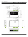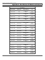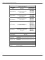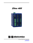
1
Zlinx Wireless I/O Manual Documentation Number: pn 7517_ZlinxIO-0111m Zlinx Wireless I/O Documentation Number: ZlinxIO-3609m This product was designed and manufactured in Ottawa, Illinois USA Using domestic and imported parts by International Headquarters B&B Electronics Mfg. Co. Inc. 707 Dayton Road Ottawa, IL 61350 USA Phone: (815) 433-5100 General Fax: (815) 433-5105 Website: www.bb-elec.com European Headquarters B&B Electronics Ltd. Westlink Commercial Park Oranmore, Co. Galway, Ireland Phone: (+353) 91-792444 Fax: (+353) 91-792445 Website: www.bb-europe.com ____________________________________________________________________________________________________ ©2009 B&B Electronics Mfg Co Inc. No part of this publication may be reproduced or transmitted in any form or by any means, electronic or mechanical, including photography, recording, or any information storage and retrieval system without written consent. Information in this manual is subject to change without notice, and does not represent a commitment on the part of B&B Electronics Mfg Co Inc. B&B Electronics Mfg Co Inc. shall not be liable for incidental or consequential damages resulting from the furnishing, performance, or use of this manual. All brand names used in this manual are the registered trademarks of their respective owners. The use of trademarks or other designations in this publication is for reference purposes only and does not constitute an endorsement by the trademark holder. ii Manual Documentation Number: pn7515_ZlinxIO-0111m CONTENTS 1. OVERVIEW ..................................................................................................................................................................................... 1 1.1 1.2 1.3 1.4 1.5 1.6 NOTICES ..................................................................................................................................................................................... 1 PREREQUISITES ........................................................................................................................................................................... 1 SAFETY INFORMATION ................................................................................................................................................................ 1 UL & CUL INSTALLATION INFORMATION ................................................................................................................................... 1 ABOUT THIS MANUAL ................................................................................................................................................................. 3 ZLINX WIRELESS I/O PRODUCT SPECIFICATION SUMMARY ........................................................................................................ 5 2. PRODUCT INTRODUCTION ....................................................................................................................................................... 6 2.1 ZLINX WIRELESS I/O PRODUCT FAMILY ..................................................................................................................................... 6 2.2 ZLINX WIRELESS I/O MODES OF OPERATION ............................................................................................................................. 6 2.2.1 Peer-to-Peer Mode .......................................................................................................................................................... 6 2.2.2 Modbus Mode .................................................................................................................................................................. 7 2.2.3 Repeater Mode ................................................................................................................................................................ 8 2.2.3.1 Configuring Modbus Radio Modem as a repeater ............................................................................................................................. 8 2.3 PACKAGE CONTENTS .................................................................................................................................................................. 9 2.4 FEATURES ................................................................................................................................................................................. 10 2.5 RADIO FREQUENCY BASICS ...................................................................................................................................................... 11 2.5.1 What is dBm? ................................................................................................................................................................. 11 2.5.2 Lower Frequencies - Better Propagation ................................................................................................................... 11 2.5.3 Range Performance ...................................................................................................................................................... 11 2.5.4 RF Noise ......................................................................................................................................................................... 12 2.5.5 Fade Margin ................................................................................................................................................................... 12 2.5.6 Remember Your Math .................................................................................................................................................. 12 2.5.7 RF Attenuation and Line of Sight ................................................................................................................................ 12 2.5.7.1 2.5.7.2 2.5.7.3 Path Loss Rules of Thumb ............................................................................................................................................................... 13 Antennas .......................................................................................................................................................................................... 13 Cable Loss ....................................................................................................................................................................................... 14 3. HARDWARE INFORMATION ................................................................................................................................................... 15 3.1 RECOMMENDED PRACTICE BEFORE INSTALLATION .................................................................................................................. 15 3.2 ZLINX WIRELESS I/O MODULES ............................................................................................................................................... 15 3.2.1 Base Modules ................................................................................................................................................................ 16 3.2.2 Expansion Modules ....................................................................................................................................................... 16 3.2.3 Configuration Box .......................................................................................................................................................... 17 3.3 I/O OPTIONS AND CHARACTERISTICS ....................................................................................................................................... 17 3.3.1 I/O Options ..................................................................................................................................................................... 17 3.3.2 I/O Types and Characteristics ..................................................................................................................................... 18 3.3.2.1 3.3.2.2 3.3.2.3 3.3.2.4 Digital Inputs ................................................................................................................................................................................... 18 Digital Outputs................................................................................................................................................................................. 18 Analog Inputs................................................................................................................................................................................... 18 Analog Outputs ................................................................................................................................................................................ 18 3.3.3 I/O Wiring ........................................................................................................................................................................ 20 3.3.4 Modbus I/O Addressing ................................................................................................................................................ 25 3.3.3.1 3.3.3.2 3.3.3.3 3.3.3.4 3.3.3.5 3.3.4.1 DI Wiring ......................................................................................................................................................................................... 20 DO Wiring ....................................................................................................................................................................................... 20 AI Wiring ......................................................................................................................................................................................... 21 AO Wiring ....................................................................................................................................................................................... 22 RTD Wiring ..................................................................................................................................................................................... 25 Function Field and Modbus I/O Addressing .................................................................................................................................... 27 3.3.5 Modbus Counters .......................................................................................................................................................... 27 3.4 ACCESSORIES ............................................................................................................................................................................ 28 3.4.1 LED Indicators ............................................................................................................................................................... 28 3.4.1.1 3.4.1.2 3.4.1.3 3.4.1.4 Power LED ...................................................................................................................................................................................... 28 RSSI LED ........................................................................................................................................................................................ 28 RF Data LED ................................................................................................................................................................................... 28 Bus LED .......................................................................................................................................................................................... 28 Manual Documentation Number: pn7515_ZlinxIO-0111m ··························································································································· iii 3.4.2 3.4.3 Antennas ......................................................................................................................................................................... 28 Connectors ..................................................................................................................................................................... 29 3.4.4 Mounting Hardware ....................................................................................................................................................... 31 3.4.3.1 3.4.3.2 3.4.3.3 3.4.3.4 3.4.3.5 Antenna Connector .......................................................................................................................................................................... 29 Power Supply Connector ................................................................................................................................................................. 29 Serial Port Connector ....................................................................................................................................................................... 29 Local Bus Connectors ...................................................................................................................................................................... 29 I/O Connectors ................................................................................................................................................................................. 30 4. SETUP............................................................................................................................................................................................. 32 4.1 ZLINX WIRELESS I/O INSTALLATION ........................................................................................................................................ 32 4.1.1 Power Supply Requirements ....................................................................................................................................... 32 4.1.2 RF Site Considerations................................................................................................................................................. 32 4.1.3 Zlinx Wireless I/O Mounting ......................................................................................................................................... 33 4.2 COMPUTER SYSTEM REQUIREMENTS ........................................................................................................................................ 33 4.3 INSTALLING ZLINX WIRELESS I/O SOFTWARE .......................................................................................................................... 33 4.4 INSTALLING ZZ-PROG1-USB DRIVERS ................................................................................................................................... 33 4.5 CONNECTING ZLINX WIRELESS I/O TO A PC ............................................................................................................................ 34 4.6 STARTING ZLINX I/O CONFIGURATION ..................................................................................................................................... 34 4.7 ZLINX I/O CONFIGURATION OPTIONS ....................................................................................................................................... 37 4.7.1 Information Tab.............................................................................................................................................................. 37 4.7.2 Configuration Tab .......................................................................................................................................................... 37 4.7.3 Input/Output Tab............................................................................................................................................................ 37 5. CONFIGURATION & OPERATION ......................................................................................................................................... 38 5.1 CONFIGURING ZLINX WIRELESS I/O ......................................................................................................................................... 38 5.1.1 Wireless Settings ........................................................................................................................................................... 38 5.1.2 Modbus Mode Settings ................................................................................................................................................. 43 5.1.3 Peer-to-Peer Mode Settings ........................................................................................................................................ 45 5.1.3.1 5.1.3.2 5.1.4 5.1.5 5.1.5.1 5.1.5.2 5.1.5.3 Peer-to-Peer Master ......................................................................................................................................................................... 45 Peer-to-Peer Slave............................................................................................................................................................................ 46 Input/Output Settings .................................................................................................................................................... 47 Exception Reporting ...................................................................................................................................................... 50 Sample Modbus Exception Packet ................................................................................................................................................... 51 Digital Exception Format ................................................................................................................................................................. 51 Analog Exception Format ................................................................................................................................................................ 51 5.1.6 Calibration ...................................................................................................................................................................... 52 5.1.7 Failsafe............................................................................................................................................................................ 54 5.1.8 Communication Failure Alarm ..................................................................................................................................... 54 5.1.9 Invert Output .................................................................................................................................................................. 55 5.1.10 Zlinx I/O Monitor ............................................................................................................................................................ 55 5.1.11 Saving the Configuration .............................................................................................................................................. 56 5.2 UPDATING ZLINX I/O FIRMWARE ............................................................................................................................................. 56 5.3 DIAGNOSTICS AND TESTING ..................................................................................................................................................... 58 5.3.1 Testing Modbus Mode Operation................................................................................................................................ 58 5.3.2 Testing Peer-to-Peer Mode Operation ....................................................................................................................... 58 6. EXPECTED LATENCY ............................................................................................................................................................... 59 6.1 6.2 MODBUS MODE ........................................................................................................................................................................ 59 PEER-TO-PEER MODE ............................................................................................................................................................... 60 7. RECEIVE SENSITIVITY............................................................................................................................................................. 61 8. SOFTWARE SUPPORT ............................................................................................................................................................... 62 8.1 8.2 8.3 8.4 8.5 iv SUPPORT CD INFORMATION ..................................................................................................................................................... 62 MENU ....................................................................................................................................................................................... 62 ONLINE DOCUMENTATION ........................................................................................................................................................ 62 GETTING DOCUMENTS IN HARDCOPY ....................................................................................................................................... 62 B&B ELECTRONICS INFORMATION ........................................................................................................................................... 63 Manual Documentation Number: pn7515_ZlinxIO-0111m 9. TROUBLESHOOTING ................................................................................................................................................................ 64 9.1 TESTING DIGITAL AND ANALOG I/O ......................................................................................................................................... 65 9.1.1 Testing DI ....................................................................................................................................................................... 65 9.1.2 Testing DO with Sourcing Driver ................................................................................................................................. 66 9.1.3 Testing DO with Sinking Driver ................................................................................................................................... 66 9.1.4 Testing AI in “Voltage” Mode ....................................................................................................................................... 67 9.1.5 Testing AO in “Voltage” Mode ..................................................................................................................................... 67 9.1.6 Testing AI in “Current” Mode ....................................................................................................................................... 68 9.1.7 Testing RTD module ..................................................................................................................................................... 68 APPENDIX A: DEFAULT CONFIGURATION SETTINGS .......................................................................................................... 70 APPENDIX B: PRODUCT SPECIFICATIONS ............................................................................................................................... 71 APPENDIX C: DIMENSIONAL DIAGRAMS .................................................................................................................................. 74 APPENDIX D: MODBUS I/O ASSIGNMENTS................................................................................................................................ 75 APPENDIX E: ZLINX WIRELESS I/O MODELS AND FEATURES ........................................................................................... 82 APPENDIX F: RTD MODULE ........................................................................................................................................................... 85 APPENDIX G: ZZ-4AO-2 MODULE ................................................................................................................................................. 87 APPENDIX I: CONVERT VOLTAGE TO DAC .............................................................................................................................. 90 PRODUCT UPDATES .......................................................................................................................................................................... 91 GLOSSARY ........................................................................................................................................................................................... 93 INDEX .................................................................................................................................................................................................... 95 Manual Documentation Number: pn7515_ZlinxIO-0111m ····························································································································v Overview 1. 1.1 Overview Notices This equipment has been tested and found to comply with the limits for Class A digital device, pursuant to Part 15 of the FCC Rules. These limits are designed to provide reasonable protection against harmful interference when the equipment is operated in a commercial environment. This equipment generates, uses, and can radiate radio frequency energy and, if not installed and used in accordance with the instructions, may cause harmful interference to radio communications. Operation of this equipment in a residential area is likely to cause harmful interference, in which case the user will be required to correct the interference at personal expense. Operation is subject to the following two conditions: This device may not cause harmful interference. This device must accept any interference received, including interference that may cause undesired operations. This device must be operated as supplied by B&B Electronics. Any changes or modifications made to the device without the written consent of B&B Electronics may void the user’s authority to operate the device. 1.2 Prerequisites This manual assumes that you have basic electronics knowledge and basic understanding of wireless communications. 1.3 Safety Information Exposure to RF energy is an important safety consideration. The FCC has adopted a safety standard for human exposure to radio frequency electromagnetic energy emitted by FCC regulated equipment as a result of its actions in Docket 93-62 and OET Bulleting 65 Edition 97-01. DO NOT: Operate unless all RF connectors are secure and any open connectors are properly terminated. Operate the equipment near electrical blasting caps or in an explosive atmosphere. All equipment must be properly grounded for safe operations. All equipment should be serviced only by a qualified technician. 1.4 UL & cUL Installation Information Electrical Ratings INPUT: Base Modules: ZZxxD-NA,NB-xx-xx, 10.0 - 40.0 VDC or 24 VAC, 2.7A maximum, Class 2. ZZxxD-NC,ND-xx-xx, 10.0 – 40.0 VDC or 24 VAC, 2.7A maximum, Class 2. Expansion Modules (Class 2 power derived from base modules): ZZ-2AI2AO, ZZ-4AI, ZZ-4AO, ZZ-4DI4DO-DCT1, ZZ-4RTD1, ZZ-8DI-DC, ZZ-8DO-R, ZZ-8DO-T1, ZZ-PROG1-USB: 10.0 - 40.0 VDC @ 210mA and 5.0 VDC 85 mA ZZ-4AO-2: 10 – 40 Vdc or 24 Vac, 5 Vdc @ 50 mA, 1.1W ZZ-4DI4DO-DCT, ZZ-8DO-T: 10.0 - 40.0 VDC @ 340 mA Maximum, and 5.0 VDC@50 mA Maximum OUTPUT: ZZ-8DO-R: relay output - 250 VAC, 2AGeneral Purpose/point, 8A General Purpose total All other models – Low Voltage, Limited Energy communications protocol Manual Documentation Number:pn7515_ ZlinxIO-0111m 1 Overview Special Precautions for UL and cUL Class I DIV 2 (C1D2) The following modules are class 1 Div 2 listed: - ZZ24D-Nx-SR (2.4GHz, Short range base I/O Modules) - ZZ9D-Nx-LR (900 MHz, Long range base I/O Modules) - ZZ-2AI2AO - ZZ-4AI - ZZ-4AO - ZZ-4AO-2 - ZZ-4DI4DO-DCT - ZZ-4DI4DO-DCT1 - ZZ-4RTD1 - ZZ-8DI-DC - ZZ-8DO-R - ZZ-8DO-T - ZZ-8DO-T1 - ZZ-PROG1-USB Class 1, Div 2 exceptions: Note 1: ZZ-8DO-R is not UL508 listed. Note 2: ZZxxD-Nx-MR, ZZxxD-Nx-xR-AU and ZZ8D-Nx-xR models are not Class 1, Div 2 listed but are UL508 listed. WARNING – EXPLOSION HAZARD – SUBSTITUTION OF COMPONENTS MAY IMPAIR SUITABILITY FOR CLASS I, DIVISION 2 WARNING – EXPLOSION HAZARD – WHEN IN HAZARDOUS LOCATIONS, TURN OFF POWER BEFORE REPLACING ANTENNA WARNING – EXPLOSION HAZARD – DO NOT DISCONNECT EQUIPMENT UNLESS POWER HAS BEEN SWITCHED OFF OR THE AREA IS KNOWN TO BE NONHAZARDOUS THIS EQUIPMENT IS SUITABLE FOR USE IN CLASS I, DIVISION 2, GROUPS A, B, C, AND D OR UNCLASSIFIED LOCATIONS Maximum Ambient Air Temperature 85°C (185°F) for all modules except ZZ-8DO-R. For ZZ-8DO-R, maximum Ambient Air Temperature 55°C (131°F) WIRING TERMINALS: Copper wire only One conductor per terminal Wire range: 28 to 16 AWG Tightening Torque: 1.7 lb-in. Temperature rating of field wiring – 105 °C minimum (sized for 60°C ampacity). WARNING - Two DIN rail end brackets, one on each end of of the assembled system, must be installed on the DIN rail to mechanically secure the individual products. Two end brackets are supplied with each Expansion module. The information below is specific to ZZ-8DO-R ONLY: Maximum Ambient Air Temperature 55°C (131°F) Temperature Rating of Field Wiring – 105° C (221° F) minimum sized for 55° C (131°F) ampacity. WARNING – Exposure to some chemicals may degrade the sealing properties of materials used in the Sealed Relays. 2 Manual Documentation Number: pn7515_ZlinxIO-0111m Overview RECOMMENDATION – It is recommended to inspect the Sealed Relays periodically and to check for any degradation of the materials and to replace the product, not the Sealed Relays, if any degradation is found. Relay Types JS-5N-K, JS-5-K, JS-6N-K or JS-6-K manufactured by Takamisawa Electric Co Ltd., rated 10A, 250VAC, 10A, 30VDC,utilizes the following materials to maintain sealed device properties: Relay Case Relay Base Sealant Manufacturer Mitsubishi Engineering Corp. Mitsubishi Engineering Corp. Mitsubishi Engineering Corp. Mitsubishi Engineering Corp. Mitsubishi Engineering Corp. Eccobond Plastics Type 5010GN6-30(r2) Plastics 5010GN6-30M8(cc)(r2) Plastics 5010GN6-30 M8AM Plastics 5010GN6-30M8(cc)(r2) Plastics 5010GN6-30 M8AM A-316SC Relay Type APF-30305, manufactured by Panasonic Electric Works, rated 277VAC, 8A, 24VDC, 6A general use utilizes the following materials to maintain sealed device properties: Manufacturer Type Relay Case Wintech Polymer Ltd. CN7030MFBD Relay Base Wintech Polymer Ltd. CN7015MFD Sealant Resinous Kasei Co. Ltd. A-2500BK 1.5 About this manual This manual has been created to assist you in installing, configuring, and using your Zlinx Wireless I/O modules. Please read it carefully and follow the instructions to achieve best results. The manual is divided into 11 major sections as follows: Table of Contents The table of contents is hypertext linked in the electronic documentation. This allows rapid navigation to each chapter. Overview Overview section gives a general information on product standards compliance, prerequisites and safety information. Product Introduction This section covers package contents, and main features of the Zlinx Wireless I/O products. This section also contains information on radio frequency basics. Hardware Information In this section Zlinx Wireless I/0 modules are described in details. characteristics and wiring instructions. The section covers information on I/O options and Getting Started This section guides you through the installation process. Two main modes of operation: Peer-to-Peer mode and Modbus mode are introduced in this section. Configuration and Operation Information on configuring Zlinx Wireless I/O is provided in the section. Information on settings for Peer-to-Peer and Modbus mode can be found in this section. Manual Documentation Number:pn7515_ ZlinxIO-0111m 3 Overview Software Support This section provides relevant information on obtaining product support. Troubleshooting Possible problems that may be encountered and the ways to solve them are described in this section. Appendixes Appendixes include all essential reference information for Zlinx Wireless I/O modules. Information found here includes a comprehensive references and useful tables of product properties. Glossary Glossary covers main terms which are relevant to the understanding of the Zlinx Wireless I/O concept. Index Index includes major terms and page numbers where referenced in the manual. 4 Manual Documentation Number: pn7515_ZlinxIO-0111m Overview 1.6 Zlinx Wireless I/O Product Specification Summary Need to get a digital signal across a highway or river? Or just to the other end of your big warehouse? Zlinx Wireless I/O can do the job faster, easier, and less expensively than stringing cable. Easy plug-and-play set-up saves installation and maintenance time. Despite their low price, these are not wimpy consumer or office products. Zlinx Wireless I/O is built to handle the heat, cold, and environments of industrial operations. Choice of number and type of digital and analog I/O. Ranges to 25 miles. Heavy Duty DIN mount, industrial grade case and components. Frequency ranges: ISM band, 902 to 928 MHz; 2.400 to 2.4385 GHz; 868 MHz. Modulation: FSK – Frequency Shift Keying. DSSS and FHSS Technology. Signal strength indicator aids troubleshooting. 3dBi for 868, 3 dBi for 900 MHz; 2.1 dBi for 2.4 MHz RPSMA male dipole. Wide temperature range -40Cº to 80 Cº. Versatile power: 10 to 40 VDC or 24 VAC. Software for Windows 7 and XP (Home or Professional with SP1 and SP2); Windows 2000 SP4; Vista 32 bit. Rugged circuitry, wide temperature – for indoor and outside applications. Handles most industrial control power configurations and power supplies. Immediate integration into UL/cUL or CSA approved panels. Exception Reporting option. Calibration option. Failsafe option. Communication Failure Alarm option. Invert Output option Zlinx I/O Monitor option. AES Encryption – 128 Bit on SR, LR-AU, and LR-868 models; 256 Bit on LR models Software Selectable Transmitter Power on SR, LR, LR-AU, and LR-868 models Software Selectable Over-the-air Data Rate on LR and LR-AU models. Manual Documentation Number:pn7515_ ZlinxIO-0111m 5 Product Introduction 2. Product Introduction Thank you for purchasing a Zlinx Wireless I/O product! This product has been manufactured to the highest standards of quality and performance to ensure your complete satisfaction. 2.1 Zlinx Wireless I/O Product Family Zlinx Wireless I/O modules provide easy-to-use, cost-effective Peer-to-Peer or Modbus wire-replacement solutions. Figure 1 A Zlinx ZZ24D-NA-SR Base Module The Zlinx Wireless I/O family of products features a selection of operational modes, communications ranges and I/O combinations. The system is scalable making it easy to start with a few I/O points and build a system with the required I/O mix. 2.2 Zlinx Wireless I/O Modes of Operation Zlinx Wireless I/O systems can operate in Peer-to-Peer or Modbus modes. Some Base Modules can be configured as repeaters to extend the radio coverage distance. 2.2.1 Peer-to-Peer Mode In Peer-to-Peer mode two Zlinx Wireless I/O systems provide wire replacement functionality. In this mode one Base is configured as the Peer-to-Peer Master and the other as the Peer-to-Peer Slave. It does not matter which end of the link is the Master and which is the Slave. Both Base Modules must be the same model. Analog and Digital Input signals connected to AI’s and DI’s on one module appear on the corresponding AO’s and DO’s on the other module and vice versa. Any Expansion Modules included in a Peer-to-Peer system must be chosen to be complimentary. For example, if Expansion Module 1 on one end of the link on System-1 is a ZZ-4AI (4 Analog Inputs), Expansion Module 1 on the other end of the link on System-2 must be a ZZ-4AO (4 Analog Outputs). Note: Changing the the OTA data rate to 9600 on the LR model will slow the data throughput. The approximate polling rate is one second. 6 Manual Documentation Number: pn7515_ZlinxIO-0111m Product Introduction Rules for Module Compatibility The following rules of modules compatibility to run in Peer-to-Peer mode should be observed: Same number of Expansion Modules. Identical Radio units (in Base Modules). Complimentary Expansion Modules. Channel Number, Network ID, and Peer-to-Peer address must be the same for both Peer-to-Peer Master and Peerto-Peer Slave to communicate with a Peer-to-Peer Slave. Figure 2 Peer-to-Peer Mode 2.2.2 Modbus Mode In Modbus mode standard RTU Modbus messages can be sent and received between a Modbus radio modem with attached Modbus device (being Master) and a Zlinx Wireless I/O system (being Slave). Data written to output addresses in the Zlinx Wireless I/O Modbus map result in signals appearing on its outputs. Signals connected to Zlinx Wireless I/O inputs are converted and stored in Modbus input memory locations and then sent across the link as Modbus messages to the Modbus radio modem. Figure 3 Manual Documentation Number: pn7515_ZlinxIO-0111m Modbus Mode 7 Product Introduction 2.2.3 Repeater Mode When a Zlinx Wireless I/O Base Module is configured as a radio repeater it relays data from a Modbus modem or another Zlinx Wireless I/O Base Module and extends the range of communication. If a repeater is needed in a Peer-to-Peer System a repeater unit can be placed between the Master and the Slave. The repeater function is supported on the MR and ZZ9D-Nx-LR-xx models only. The repeater function gives no true indication that the data is being "repeated", although you will see the RSSI LED on the device used as a repeater indicate GREEN, YELLOW or RED. NOTE: Placing a repeater in a system will slow the system down: 10ms for ZZ9D-Nx-LR-xx 200ms for MR in Peer-to-Peer 4ms for ZZ9D-Nx-LR-xx 20ms for MR in Modbus If the repeater is desired in a Peer-to-Peer platform, it's best to use a Zlinx Wireless I/O Base Module as the repeater. Without using a repeater confirm the Peer-to-Peer Master and Slave systems are communicating. Refer to section 5.3.2 ”Testing Peer-to-Peer Mode". Once it’s established that the Master and Slave are communicating, the repeater can be introduced into the system. The Zlinx Wireless I/O module used as a repeater MUST be placed in Modbus mode. This is done to keep the repeater device from accidentally responding to Peer-to-Peer packets sent by the Master device. The repeater device must have the same Wireless parameters: "Channel", and "Network Identifier" as the Peer-to-Peer Master and Slave device. The "Repeater" feature must be selected and updated to the Zlinx Wireless I/O module being used as the repeater. To select the “Repeater” feature: 1. Go to the Zlinx I/O Configuration. 2. On the Configuration Tab enable “Repeater Mode”. 3. Make sure to select Modbus mode. The system is now configured as a repeater system and the data passed from the Master to the Slave will be passed through the repeater. You can confirm repeater function by separating the Master and Slave until they stop communicating then place the repeater in the middle of the two. 2.2.3.1 Configuring Modbus Radio Modem as a repeater If configuring a Modbus Radio Modem for repeater mode the following parameters need to be configured in addition to the Channel and Network ID. 8 Set DT = 0xFFFF Set AM = to a unique value Set RP = 0x7F Set PK = 0xC9 Set RB = 0xC9 Manual Documentation Number: pn7515_ZlinxIO-0111m Product Introduction Set RO = 0x051d Set MD = 0x04 If OTA Data Rate = 9600, ATRR and ATBR =0. Figure 4 2.3 Using a Base Module as a Repeater Package Contents Base Modules are shipped with the following items included: Zlinx Wireless I/O module. Antenna. A printed version of the Modbus Mode Zlinx I/O Quick Start Guide. A printed version of the Peer-to-Peer Mode Zlinx I/O Quick Start Guide. Expansion Modules are shipped with the following items included: Zlinx Wireless I/O module. A printed version of the Modbus Mode Zlinx I/O Quick Start Guide. A printed version of the Peer-to-Peer Mode Zlinx I/O Quick Start Guide. Configuration Modules ZZ-PROG1 is shipped with the following items included: ZZ-PROG1 Configuration Box. 6 foot DB9 male to DB9 female straight-through serial cable. A printed version of the Modbus Mode Zlinx I/O Quick Start Guide. A printed version of the Peer-to-Peer Mode Zlinx I/O Quick Start Guide. Configuration kits: Manual Documentation Number: pn7515_ZlinxIO-0111m 9 Product Introduction ZZ-PROGKIT is shipped with the following items included: ZZ-PROG1 Configuration Box. 6 foot DB9 male to DB9 female straight-through serial cable. A printed version of the Modbus Mode Zlinx I/O Quick Start Guide. A printed version of the Peer-to-Peer Mode Zlinx I/O Quick Start Guide. A CD-ROM disc with: • Zlinx I/O Manager Configuration Software. • Zlinx I/O Firmware Updater. • USB Driver for ZZ-PROG1-USB • This manual in PDF format. • The Modbus Mode Zlinx I/O Quick Start Guide in PDF. • The Peer-to-Peer Mode Zlinx I/O Quick Start Guide in PDF. ZZ-PROG1-USB is shipped with the following items included: ZZ-PROG1-USB Configuration Box with a USB interface instead of a serial interface. A printed version of the Modbus Mode Zlinx I/O Quick Start Guide. A printed version of the Peer-to-Peer Mode Zlinx I/O Quick Start Guide. 1 Meter Black USB cable. A CD-ROM disc with: • Zlinx I/O Manager Configuration Software. • Zlinx I/O Firmware Updater. • USB Driver for ZZ-PROG1-USB • This manual in PDF format. • The Modbus Mode Zlinx I/O Quick Start Guide in PDF format. • The Peer-to-Peer Mode Zlinx I/O Quick Start Guide in PDF format. 2.4 10 Features Choice of number and type of digital and analog I/O. Sourcing or sinking Digital Outputs available. Flexible and scalable by adding Expansion Modules. Wireless Modbus and Peer-to-Peer communications modes. Small, economical and configurable. Wide operating temperature range. AC or DC power sources. Four models with different radio options or different range capabilities. Power, RSSI, RF Data and Bus LED’s. Manual Documentation Number: pn7515_ZlinxIO-0111m Product Introduction 2.5 Removable screw terminal connectors for power supply and I/O points. Zlinx Manager Configuration Software. DIN rail mountable. Radio Frequency Basics 2.5.1 What is dBm? Radio Frequency (RF) power is measured in milli-Watts (mW) or, more usually in a logarithmic scale of decibels (dB), or decibels referenced to 1 mW of power (dBm). Since RF power attenuates as a logarithmic function, the dBm scale is most useful. Here are some examples of how these scales relate: 1mW = 0dBm 2mW = 3dBm 4mW = 6dBm A 2-fold increase in power yields 3dBm of signal. A 10-fold increase in power yields 10dBm of signal. A 100-fold increase in power yields 20dBm of signal. 10mW = 10dBm 100mW = 20dBm 1W = 30dBm Figure 5 The dDm scale 2.5.2 Lower Frequencies - Better Propagation Industrial applications typically operate in “license free” frequency bands, also referred to as ISM (Industrial, Scientific, and Medical). The frequencies and power of these bands varies from country to country. The most common frequencies encountered are: 2.4 GHz – nearly worldwide. 915 MHz band – North America, South America, and some other countries. 868 MHz band – Europe. As frequency rises, available bandwidth typically rises, but distance and ability to overcome obstacles is reduced. For any given distance, a 2.4 GHz installation will have roughly 8.5 dB of additional path loss when compared to 900 MHz. However, lower frequencies require larger antennas to achieve the same gain. 2.5.3 Range Performance The more sensitive the radio is, the lower the power signal it can successfully receive, stretching right down to the noise floor. There is so much variety in specifications for radio sensitivity, that it is difficult to make a meaningful comparison between products. The most meaningful specification is expressed at a particular bit error rate and will be given for an ideal environment shielded from external noise. Unless you are in a high RF noise environment, typically resulting from numerous similar-frequency radio transmitters located nearby, the odds are good that the noise floor will be well below the receive sensitivity, so the manufacturer’s rated receive sensitivity will be a key factor in your wireless system and range estimates. You can often improve your receive sensitivity, and therefore your range, by reducing data rates over the air. Receive sensitivity is a function of the transmission baud rate so, as baud rate goes down, the receive sensitivity goes up. Many radios give the user the ability to reduce the baud rate to maximize range. The receive sensitivity of a radio also improves at lower frequencies, providing another significant range advantage of 900 MHz (vs. 2.4 GHz) - as much as six to twelve dB! Manual Documentation Number: pn7515_ZlinxIO-0111m 11 Product Introduction 2.5.4 RF Noise RF background noise comes from many sources, ranging from solar activity to high frequency digital products to all forms of other radio communications. That background noise establishes a noise floor which is the point where the desired signals are lost in the background ruckus. The noise floor will vary by frequency. Typically the noise floor will be lower than the receive sensitivity of your radio, so it will not be a factor in your system design. If, however, you’re in an environment where high degrees of RF noise may exist in your frequency band, then use the noise floor figures instead of radio receive sensitivity in your calculations. If you suspect this is the case, a simple site survey to determine the noise floor value can be a high payoff investment. When in doubt, look around. Antennas are everywhere nowadays - on the sides of buildings, water towers, billboards, chimneys, even disguised as trees. Many sources of interference may not be obvious. 2.5.5 Fade Margin Fade margin is a term critical to wireless success. Fade margin describes how many dB a received signal may be reduced by without causing system performance to fall below an acceptable value. Walking away from a newly commissioned wireless installation without understanding how much fade margin exists is the number one cause of wireless woes. Establishing a fade margin of no less than 10dB in good weather conditions will provide a high degree of assurance that the system will continue to operate effectively in a variety of weather, solar, and RF interference conditions. There are a number of creative ways to estimate fade margin of a system without investing in specialty gear. Pick one or more of the following and use it to ensure you’ve got a robust installation: Some radios have programmable output power. Reduce the power until performance degrades, then dial the power back up a minimum of 10dB. Remember again, doubling output power yields 3 dB, and an increase of 10dB requires a ten-fold increase in transmit power. Invest in a small 10dB attenuator - pick the correct one for your radio frequency! If you lose communications when you install the attenuator installed in-line with one of your antennas, you don’t have enough fade margin. Antenna cable has greater attenuation at higher frequencies. Specifications vary by type and manufacturer so check them yourself but, at 900 MHz, a coil of RG58 in the range of 50 to 100 feet (15 to 30 m) will be 10dB. At 2.4GHz, a cable length of 20-40 feet (6 to 12 m) will yield 10dB. If your system still operates reliably with the test length of cable installed, you’ve got at least 10dB of fade margin. 2.5.6 Remember Your Math Contrary to popular opinion, no black art is required to make a reasonable prediction of the range of a given radio signal. Several simple concepts must be understood first, and then we can apply some simple rules of thumb. The equation for successful radio reception is: TX power + TX antenna gain – Path loss – Cabling loss + RX antenna gain – 10dB fade margin > RX Radio sensitivity or (less commonly) RF noise floor Note that most of the equation’s parameters are easily gleaned from the manufacturer’s data. That leaves only path loss and, in cases of heavy RF interference, RF noise floor as the two parameters that you must establish for your particular installation. In a perfect world, you will measure your path loss and your RF noise conditions. For the majority of us that don’t, there are rules of thumb to follow to help ensure a reliable radio connection. 2.5.7 RF Attenuation and Line of Sight In a clear path through the air, radio signals attenuate with the square of distance. Doubling range requires a four-fold increase in power, therefore: 12 Halving the distance decreases path loss by 6dB. Doubling the distance increases path loss by 6dB. Manual Documentation Number: pn7515_ZlinxIO-0111m Product Introduction When indoors, paths tend to be more complex, so use a more aggressive rule of thumb, as follows: Halving the distance decreases path loss by 9dB. Doubling the distance increases path loss by 9dB. Radio manufacturers advertise “line of sight” range figures. Line of sight means that, from antenna A, you can see antenna B. Being able to see the building that antenna B is in does not count as line of sight. For every obstacle in the path, de-rate the “line of sight” figure specified for each obstacle in the path. The type of obstacle, the location of the obstacle, and the number of obstacles will all play a role in path loss. Visualize the connection between antennas, picturing lines radiating in an elliptical path between the antennas in the shape of a football. Directly in the center of the two antennas the RF path is wide with many pathways. A single obstacle here will have minimal impact on path loss. As you approach each antenna, the meaningful RF field is concentrated on the antenna itself. Obstructions located close to the antennas cause dramatic path loss. Be sure you know the distance between antennas. This is often underestimated. If it’s a short-range application, pace it off. If it’s a long-range application, establish the actual distance with a GPS or Google Maps. The most effective way to reduce path loss is to elevate the antennas. At approximately 6 feet high (2 m), line of sight due to the Earth’s curvature is about 3 miles (5 km), so anything taller than a well-manicured lawn becomes an obstacle. Weather conditions also play a large role. Increased moisture in the air increases path loss. The higher the frequency, the higher the path loss. Beware of leafy greens. While a few saplings mid-path are tolerable, it’s very difficult for RF to penetrate significant woodlands. If you’re crossing a wooded area you must elevate your antennas over the treetops. Industrial installations often include many reflective obstacles leading to numerous paths between the antennas. The received signal is the vector sum of each of these paths. Depending on the phase of each signal, they can be added or subtracted. In multiple path environments, simply moving the antenna slightly can significantly change the signal strength. Some obstacles are mobile. More than one wireless application has been stymied by temporary obstacles such as a stack of containers, a parked truck or material handling equipment. Remember, metal is not your friend. An antenna will not transmit out from inside a metal box or through a storage tank. 2.5.7.1 Path Loss Rules of Thumb To ensure basic fade margin in a perfect line of sight application, never exceed 50% of the manufacturer’s rated line of sight distance. This in itself yields a theoretical 6dB fade margin – still short of the required 10dB. De-rate more aggressively if you have obstacles between the two antennas, but not near the antennas. De-rate to 10% of the manufacture’s line of sight ratings if you have multiple obstacles, obstacles located near the antennas, or the antennas are located indoors. 2.5.7.2 Antennas Antennas increase the effective power by focusing the radiated energy in the desired direction. Using the correct antenna not only focuses power into the desired area but it also reduces the amount of power broadcast into areas where it is not needed. Wireless applications have exploded in popularity with everyone seeking out the highest convenient point to mount their antenna. It’s not uncommon to arrive at a job site to find other antennas sprouting from your installation point. Assuming these systems are spread spectrum and potentially in other ISM or licensed frequency bands, you still want to maximize the distance from the antennas as much as possible. Most antennas broadcast in a horizontal pattern, so vertical separation is more meaningful than horizontal separation. Try to separate antennas with like-polarization by a minimum of two wavelengths, which is about 26 inches (0.66 m) at 900 MHz, or 10 inches (0.25 m) at 2.4 GHz. Manual Documentation Number: pn7515_ZlinxIO-0111m 13 Product Introduction 2.5.7.3 Cable Loss Those high frequencies you are piping to your antennas don’t propagate particularly well through cable and connectors. Use high quality RF cable between the antenna connector and your antenna and ensure that all connectors are high quality and carefully installed. Factor in a 0.2 dB loss per coaxial connector in addition to the cable attenuation itself. Typical attenuation figures per 10 feet (3 meters) for two popular cable types are listed below. Cable Types Frequency RG-58U* LMR-400* 900 MHz 1.6 dB 0.4 dB 2.4 GHz 2.8 dB 0.7 dB *Loss per 10 feet (3 meters) of cable length Figure 6 Attenuation figures While long cable runs to an antenna create signal loss, the benefit of elevating the antenna another 25 feet (7.6 m) can more than compensate for those lost dB. 14 Manual Documentation Number: pn7515_ZlinxIO-0111m Hardware Information 3. 3.1 Hardware Information Recommended Practice Before Installation Before installing a new system, it is preferable to bench test the complete system as configuration problems are easier to recognize when the system units are close together. Following installation, poor communications can be caused by: Incorrectly installed antennas. Radio interference. Obstructions in the radio path. Radio path too long. If the radio path is a problem, higher performance antennas may help. Please set up a bench test and familiarize yourself with a pair or set of these modules before taking them out into the field for installation. For testing analog and digital I/O see section 9.1”Testing Digital and Analog I/O”. 3.2 Zlinx Wireless I/O Modules Zlinx Wireless I/O encompasses a growing family of products including Base Modules, Expansion Modules, Configuration Boxes, configuration software and accessories. All modules are built into similar enclosures featuring male local bus plugs and female local bus receptacles on the sides, which allow modules to connect together (except Base Modules which do not have left-side connector and Configuration Boxes which do not have right-side connectors). Modules are DIN rail mountable and feature removable screw terminal blocks. Zlinx Wireless I/O modules are configured using a Configuration Box, connected to a PC and running Zlinx Manager Software. Zlinx Wireless I/O systems can operate in Modbus or Peer-to-Peer modes. In Modbus mode a Zlinx Wireless I/O system exchanges Modbus messages with a Modbus radio modem. In Peer-to-Peer mode two Zlinx Wireless I/O systems provide wire-replacement functionality. Some Base Modules can also be used as repeaters, to extend the communication distance of a system. NOTE: Refer to section 2.2 “Zlinx Wireless I/O Modes of Operation” for more information. Figure 7 Front View of Zlinx Wireless I/O Base, Configuration Box, and Expansion Modules, Manual Documentation Number: pn7515_ZlinxIO-0111m 15 Hardware Information 3.2.1 Base Modules Each Zlinx Wireless I/O system is built around a Base Module. Base Modules provide digital and/or analog I/O, and radio communications with other Zlinx nodes. Figure 8 A Typical Base Module (2AI-2AO-2DI-2DO) Radio options include three frequency bands 2.4 GHz, 900 MHz, and 868 MHz (868 band is applied in Europe and due to the single-channel band, to prevent excessive interference between radios regulations require radios to not exceed a 10% transmission duty cycle. This means that the radio can only be transmitting 10% of the time), and three power output/range categories: Short Range, Medium Range, and Long Range. Frequency Band 2.4 GHz 2.4 GHz 900 MHz 900 MHz 868 MHz Figure 9 Range Category Short Range (SR) Medium Range (MR) Medium Range (MR) Long Range (LR) Long Range (LR) Indoor Outdoor (Line of Sight) 300 ft 1 mile 600 ft 3 miles 1500 ft 7 miles 1800 ft 25 miles 1800 ft 25 miles Radio Type Options and Ranges (with included antennas) Several different combinations of Digital Inputs (DI), Digital Outputs (DO), Analog Inputs (AI) and Analog Outputs (AO) are available. For example, the ZZ24D-NA-SR features a combination of two DI’s, two DO’s, two AI’s, and two AO’s in a package with a short range (SR) 2.4 GHz radio option. Similar models are available with Medium Range (MR) and Long Range (LR) radio options. 3.2.2 Expansion Modules Up to six Expansion Modules can be plugged into the Base Module to add more I/O capabilities in any combination needed. For example, the ZZ-8DO-T Expansion Module provides eight additional Digital Outputs; the ZZ-2AI2AO provides two Analog Inputs and two Analog Outputs. NOTE: Refer to “Appendix E: Zlinx Wireless I/O Models and Features” for a list of Zlinx Wireless I/O models and features. Expansion Modules connect to Base Modules by plugging the modules together, engaging the local bus connectors located on the sides of the boxes. Male plugs on Expansion Modules plug into female connectors on the side of the Base Module or 16 Manual Documentation Number: pn7515_ZlinxIO-0111m Hardware Information other Expansion Modules, resulting in a horizontal “stack” with the Base Module on the left and Expansion Modules extending to the right. Figure 10 Base and Expansion Modules Connected Together 3.2.3 Configuration Box The ZZ-PROG1 or ZZ-PROG1-USB Configuration Boxes provide a convenient way to interface Base and Expansion Modules with a PC and the software used to configure them. The Configuration Box plugs into a Base or Expansion Module on the right hand side. The Configuration Box connects to a PC serial port (COM1 to 16) using a standard straight-through 9pin serial cable unless you are using the ZZ-PROG1-USB model which uses a USB cable. Figure 11 3.3 A PC, Configuration Box and Base Module I/O Options and Characteristics 3.3.1 I/O Options The Zlinx Wireless I/O family of products features a variety of input and output options. Base and Expansion Module options include: 2 Analog Inputs, 2 Analog Outputs, 2 Digital Inputs and 2 Digital Outputs (sourcing or sinking driver). 4 Digital Inputs and 4 Digital Outputs (sourcing or sinking driver). 8 Digital Inputs. 8 Digital Outputs (sourcing or sinking driver) and relay. Manual Documentation Number: pn7515_ZlinxIO-0111m 17 Hardware Information 4 Analog Inputs. RTD Temperature input module. 4 Analog Outputs. 2 Analog Inputs and 2 Analog Outputs. Modules continue to be developed with additional features and options. NOTE: Refer to “Appendix E: Zlinx Wireless I/O Models and Features” for a list of available models and options. 3.3.2 I/O Types and Characteristics 3.3.2.1 Digital Inputs DI’s can detect the presence of contact closures, transistor switches or on/off DC voltage signals (low or high logic levels). Voltages below 0.8 VDC are interpreted as a low state. Voltages between 4.0 VDC and 48 VDC are interpreted as a high state. The state of voltages between 0.8V and 4.0V are undefined. In Peer-to-Peer mode the outputs are active because the Digital Inputs on the corresponding complimentary system are pulled high. Connecting the Digital Inputs to a 10K pull down resistor would bring the DO’s low or inactive as a default. NOTE: Inputs have an internal “weak” pull-up resistor so unconnected inputs will read as being in the high state. 3.3.2.2 Digital Outputs Digital Outputs send on/off signals (low or high logic levels) to drive external devices such as indicators, relay coils or the inputs of other equipment such as PLC’s, SCADA, etc. Modules with Digital Outputs are available with sourcing or sinking drivers and relay. Sourcing (PNP transistor) drivers provide up to 40mA per output (or 320mA total for an 8 DO module) at output voltages up to 40 VDC to connected loads. Sinking (NPN transistor) drivers can sink up to 40 mA per output (or 320mA total for an 8 DO module) at voltages up to 48 VDC. 3.3.2.3 Analog Inputs Analog Inputs accept voltage, current signals, or RTD temperature signals. When configured as voltage inputs the full range is 0 to 10 VDC. When configured as current inputs the full range is 0 to 20mA and the input resistance is 250 Ω. When configured as an RTD input, the range varies based on the RTD Probe. Supported Probe types include Pt100, Pt1000, Cu10. NOTE: 0 to 20mA AI’s accommodate standard 4 to 20mA instrumentation current loop signals. 3.3.2.4 Analog Outputs Analog Outputs produce voltage or current output signals. When configured as voltage outputs the full range is 0 to 10 VDC at 1mA maximum. When configured as current outputs the full range is 0 to 20mA with a maximum load resistance of 450 Ω at 12V. For all models except the ZZ-4AO-2, the 0-20mA output circuit is comprised of an open collector sinking output. This means that an external supply will be required to properly setup the current loop. This type of circuit sinks the current to a common ground, which will require the use of either a differential input type or an isolator in-between the output and input circuits. 18 Manual Documentation Number: pn7515_ZlinxIO-0111m Hardware Information NOTE: 0 to 20mA AO’s accommodate standard 4 to 20mA instrumentation current loop signals. Manual Documentation Number: pn7515_ZlinxIO-0111m 19 Hardware Information 3.3.3 I/O Wiring 3.3.3.1 DI Wiring The following diagram shows typical connection wiring for various Digital Inputs: Figure 12 Typical Digital Input Wiring for Various Input Devices (ZZ-4DI4D0-DCT Expansion Module) NOTE: No external power supply wiring is required for Expansion Modules. 3.3.3.2 DO Wiring The following diagram shows typical connection wiring for modules featuring sourcing (PNP) drivers: Figure 13 20 Typical Digital Output Wiring for Sourcing Outputs (ZZ-4DI4D0-DCT Expansion Module) Manual Documentation Number: pn7515_ZlinxIO-0111m Hardware Information The following diagram shows typical connection wiring for modules featuring relay drivers: Figure 14 Typical Digital Output Wiring for Relay Outputs The following diagram shows typical connection wiring for modules featuring sinking (NPN) drivers: Figure 15 Typical Digital Output Wiring for Sinking Outputs (ZZ-4DI4D0-DCT1 Expansion Module) 3.3.3.3 AI Wiring The following diagram shows typical connection wiring for Analog Inputs (both current and voltage inputs): Figure 16 Manual Documentation Number: pn7515_ZlinxIO-0111m Typical Analog Input Wiring (ZZ9D-NA-MR Base Module) 21 Hardware Information The following diagram shows typical connection wiring for Analog Inputs configured as voltage signals: Figure 17 Typical Analog Input Wiring (Voltage) 3.3.3.4 AO Wiring The following diagram shows typical connection wiring for Analog Outputs. When used as current outputs (0-20mA setting), the analog outputs in the Zlinx base and expansion modules (except ZZ-4AO-2) are sinking type. When used as voltage outputs (0-10Vdc), analog outputs from all the modules are sourcing type. Current output Configuration (all Zlinx Gen II modules except ZZ-4AO-2): An external voltage source is necessary and should be connected as shown below: Figure 18 Typical Analog Output Wiring (ZZ9D-NA-MR Base Module) 22 Manual Documentation Number: pn7515_ZlinxIO-0111m Hardware Information Current output Configuration (for ZZ-4AO-2): Figure 19A Typical Analog Output Wiring (ZZ-4AO-2 Module) Manual Documentation Number: pn7515_ZlinxIO-0111m 23 Hardware Information When configured as a voltage output, the analog outputs are of sourcing type. The following diagram shows typical Analog Output Wiring for Sourcing drivers: Analog output connection for Sourcing drivers: Figure 20 Typical Analog Output Wiring for Sourcing Outputs Voltage output Configuration (all Zlinx Gen II modules): The following diagram shows typical Analog Output Wiring for Sourcing outputs configured as voltage signals: Figure 21 Typical Analog Output Wiring for Sourcing Outputs (Voltage) 24 Manual Documentation Number: pn7515_ZlinxIO-0111m Hardware Information 3.3.3.5 RTD Wiring The following diagram shows typical connection wiring for RTD inputs: Figure 22 Typical RTD Input Wiring 3.3.4 Modbus I/O Addressing Zlinx Wireless I/O modules can be configured to operate as wireless Modbus nodes. The Modbus device should be connected to the Modbus radio modem. In Modbus mode messages are sent across the wireless link from a Modbus radiomodem to the Zlinx Wireless I/O and from the Zlinx Wireless I/O to the Modbus radio-modem. Digital and Analog Input information from the Zlinx Wireless I/O inputs is stored in the Zlinx Wireless I/O memory and then sent across the link to the Modbus modem. Digital and Analog Output information is sent from the Modbus modem to the Zlinx Wireless I/O, stored in its memory, and then sent to the outputs. To use Modbus mode successfully, an understanding of the Zlinx Wireless I/O memory map assignments is necessary. What is a Modbus Map? A Modbus Map is simply a list for an individual slave device that defines: What the data is (ex. pressure or temperature readings). Where the data is stored (which tables and data addresses). How the data is stored (data types, byte and word ordering). Some devices are built with a fixed map that is defined by the manufacturer, while other devices allow the operator to configure or program a custom map to fit their needs. Modbus function codes supported: Function 1: Read DO Status Function 2: Read DI’s Function 3: Read AO Status Function 4: Read AI’s Function 5: Write to Single DO (firmware v2.0 or higher) Function 6: Write to Single AO Function 15: Write to Multi DO’s Messages sent between Zlinx Wireless I/O and a Modbus modem use Modbus memory addresses to specify what type of information is being sent and where it is stored. In the Modbus addressing scheme each type of I/O (DO, DI, AI, and AO) is stored in a different section of the memory. Manual Documentation Number: pn7515_ZlinxIO-0111m 25 Hardware Information I/O Type Modbus Memory Address DO DI AI AO 00001 to 00112 10001 to 10112 30001 to 30112 40001 to 40112 Figure 23 I/O Memory Areas Table Within these sections, addresses are reserved for all Zlinx Wireless I/O modules that may be used. Module Base Expansion 1 Expansion 2 Expansion 3 Expansion 4 Expansion 5 Expansion 6 Figure 24 Memory Range n0001 to n0016 n0017 to n0032 n0033 to n0048 n0049 to n0064 n0065 to n0080 n0081 to n0096 n0097 to n0112 Module I/O Addressing Table NOTE: In the table “n” is a single digit between 0 and 4. The following examples show how the addressing works: Example 1: To turn on the second Digital Output (DO2) on the Base Module, the Modbus modem sends a message placing a logic 1 in memory location 00002. Example 2: To cause Expansion Module 3 to output a specified voltage on AO1, the Modbus modem sends a message to set the register at Modbus address 40049 to the appropriate value. Refer to “Appendix I: Convert Voltage to DAC” for the information on how to convert voltages to DAC. A list of all Modbus address assignments for all Zlinx Wireless I/O points is shown in Appendix D: Modbus I/O Assignments”. Several important points about this list should be noted: Some addresses are listed but not implemented in current versions of Zlinx Wireless I/O hardware. “Appendix D: Modbus I/O Assignments”. Refer to Some addresses are reserved for internal Zlinx Wireless I/O use. Some addresses are reserved for future use. 40000 series addresses store Analog Output data AND Counter data when Digital Inputs are configured for Counter operation. For each module, the first eight memory locations are assigned to AO data and the next four locations (7 for Base and 2 for Expansion Modules) are assigned to Counter data. NOTE: For more information on Counters, see section 3.3.5“Modbus Counters”. If a Modbus device communicating with Zlinx Wireless I/O tries to send to or receive from a memory address not implemented by the hardware in use, the Zlinx Wireless I/O replies with an exception response. NOTE: “Appendix D: Modbus I/O Assignments” of this manual contains a list of Modbus I/O assignments for the Zlinx Wireless I/O. 26 Manual Documentation Number: pn7515_ZlinxIO-0111m Hardware Information 3.3.4.1 Function Field and Modbus I/O Addressing Modbus Function Code The function code in the Master device query tells the addressed slave device what kind of action to perform. The data bytes contain any additional information that the slave will need to perform the function. For example, function code 03 will query the slave to read holding registers and respond with their contents. The data field must contain the information telling the slave which register to start at and how many registers to read. Modbus I/O addressing The Modbus protocol allows for two types of I/O addressing: implied and extended. Implied addressing uses the function code to determine the I/O address and only requires the minimum address; i.e. 40012 = 0x0C, the 4nnnn is implied. The extended address contains the entire I/O address; i.e. 40012 = 0x9C4C. Another example: Using holding register 40108 to address a DAC or analog output. The function code field already specifies a “holding register” operation. Therefore the “4nnnn” reference is implicit. Holding register 40108 is addressed as register 0x006B (107 decimal). The B&B Zlinx series of remote I/O devices uses the implied I/O addressing method. If your device is sending the full extended I/O address, an error will occur. 3.3.5 Modbus Counters Base Modules In Modbus mode a Base Module supports two Digital Inputs as counters: Frequency. Accumulators. There are four accumulator registers on only the Base Module which hold accumulators information – two for each Digital Input. Accumulator most significant count register 400nn displays the respective count from 0 to 9999. Accumulator least significant count register 400nn displays the respective count from 0 to 9999. This will increment the most significant count when it rolls over from 9999 to 0. Time to save totals register counts down the number of seconds (from 300-0 seconds) until the Accumulators are saved internally. Expansion Modules In Modbus mode Expansion Module supports two Digital Inputs as frequency. There are two frequency registers on each module which hold frequency information – one for each Digital Input. Register addresses for frequency will be found at 40nnn, (where “n” is a single digit between 0 and 9). NOTE: For more information see “Appendix D: Modbus I/O Assignments”. Accumulators A typical electric water meter will generate a pulse per 1/10 gallon of water flowing through it. This type of application is best used with the Modbus accumulators. The accumulators are broken down into two registers, most significant count and least significant count. Both accumulators have a full count of 9999. When the least significant count exceeds 9999, it will increment the most significant count giving a total system count of 99,999,999. Manual Documentation Number: pn7515_ZlinxIO-0111m 27 Hardware Information The accumulators reside in the holding register map and maybe written to in order to reflect what a typical water meter may have displayed on its display. There is also a holding register associated with the accumulators that indicates the number of seconds before the accumulators are saved. The accumulator data is saved every ~5min. Frequency Flow meters typically generate a frequency based on the amount of fluid flowing through the sensor. The flow and respective frequency varies on the manufacture and sensor. The frequency measurement is located in a separate Modbus holding register and may not be written to. The frequency register is formatted in cycles/sec and requires the user to convert the frequency to respective flow units 3.4 Accessories 3.4.1 LED Indicators Base Modules have four LED indicators: a Power LED, an RSSI LED, a Wireless Data LED, and a Local Bus Data LED. Expansion Modules and Configuration Boxes have two LED’s: a Power LED and a Local Bus Data LED. 3.4.1.1 Power LED The Power LED illuminates (red) immediately on power up indicating that AC or DC power is present on the power supply terminals. 3.4.1.2 RSSI LED The RSSI LED provides an indication of the signal strength of the received radio signal. The color of the LED indicates whether the signal is weak, OK, or strong. The table below explains the colors of RSSI LED: LED Color Signal Strength Off Red Yellow Green No signal Weak OK Strong Figure 25 RSSI LED Status Table NOTE: Data can be sent and received for Weak, OK, and Strong Signal. 3.4.1.3 RF Data LED The RF Data LED blinks green when data is being transmitted or received on the radio link. When the LED is off no data is being transmitted or received. 3.4.1.4 Bus LED The Bus LED blinks green when data is being transmitted or received on the local bus connection. When the LED is off no data is being transmitted or received. NOTE: If communications is not established within a preset number of retries (default is 10) the RF Data and Bus LED’s blink alternately to indicate a loss of communications. 3.4.2 Antennas Base Modules operating in the 900 MHz band come equipped with 6.5-inch folding rubber duck antennas (ZZ9D-ANT1) that screw onto the reverse SMA connector on top of the case. Base Modules operating in the 2.4 GHz band come equipped with 4.25-inch, folding rubber duck antennas (ZZ24D-ANT1). Higher gain antennas may be connected to extend the range. 28 Manual Documentation Number: pn7515_ZlinxIO-0111m Hardware Information 3.4.3 Connectors Zlinx Wireless I/O Base and Expansion Modules feature connectors for connecting field I/O wiring and plugging together Zlinx Wireless I/O modules (local bus). In addition, Base Modules include connectors for connecting an antenna and power supply. Configuration Boxes include a serial connector for connecting to a PC COM port or if using the ZZ-PROG1-USB then a USB connector is provided for connecting to the PC. 3.4.3.1 Antenna Connector Base Modules have a reverse SMA antenna connector mounted on the top edge of the enclosure. Figure 26 Top View of a Base Module 3.4.3.2 Power Supply Connector The Power Supply connector (Base Modules only) is a two-position removable terminal block located on the top of the unit. Terminal spacing is 3.5 mm. The terminal block accepts solid and stranded wires from 28 AWG to 16 AWG. Please check polarity marking in Figure 26. NOTE: Refer to section 4.1.1 “Power Supply Requirements” for more information. The Configuration Box and all Expansion Modules receive power from the Base Module via the local bus connector. 3.4.3.3 Serial Port Connector The Serial Port connector (Configuration Box only) is a DB-9F (female) connector which comes on the ZZ-PROG1. The Configuration Box is configured as a DCE. For programming, a standard straight-through serial cable with DB-9F on one end and DB-9M on the other is required. (Part No. 9PAMF6 recommended) Figure 27 DB-9 Female Serial Port Connector with Pin-out 3.4.3.4 Local Bus Connectors The Local Bus connectors are included on Base, Expansion, and Configuration Boxes. These connectors are dual row, 14 pin (2 mm spacing) connectors, male on one side of the module and female on the other (except Base Modules which don’t have left-side connector and Configuration boxes which don’t have right-side connector). Modules are plugged together to supply power and facilitate communication between modules. When adding an Expansion Module to a Base Module the male connector on the Expansion Module plugs into the female connector on the Base Module. The second Expansion Module plugs into the first, and so on, up to a maximum of six Expansion Modules. Manual Documentation Number: pn7515_ZlinxIO-0111m 29 Hardware Information Figure 28 ZZ-TB1 Accessory Kit Contents The Configuration Box should be installed on the right hand side of the system. 3.4.3.5 I/O Connectors I/O connectors for Base and Expansion Modules are removable (plug in) screw terminal blocks located on the front of the unit. Terminal spacing is 3.5 mm. Depending on the specific model, the number of terminals may vary. The maximum is 16 terminals (two 8-terminal blocks). Extra terminal blocks are available in an accessory kit (ZZ-TB1). The kit includes: Item 2-position terminal block 4-position terminal block 8-position terminal block Shroud cover Figure 29 Quantity 2 2 2 1 ZZ-TB1 Accessory Kit Contents NOTE: For information on replacement parts refer to “Appendix B: Product Specifications”. 30 Manual Documentation Number: pn7515_ZlinxIO-0111m Hardware Information 3.4.4 Mounting Hardware Zlinx Wireless I/O modules can be DIN rail mounted. The DIN mounting clip and spring is included on each module. Figure 30 Manual Documentation Number: pn7515_ZlinxIO-0111m DIN Clip with Spring on a Zlinx Wireless I/O Module 31 Setup 4. 4.1 Setup Zlinx Wireless I/O Installation 4.1.1 Power Supply Requirements Zlinx Wireless I/O systems can be powered from DC or AC power sources. No supply is included since the power rating of the supply will depend on the total power requirements of all modules used in the system. NOTE: “Appendix B: Product Specifications” contains a listing of power requirements for all Zlinx Wireless I/O modules. If an AC power supply is to be used, it must be 24VAC. If a DC power supply is to be used, it must be 10-40VDC. NOTE: 110/220/240 VAC mains power must NOT be connected to any input terminal on Zlinx Wireless I/O modules. 4.1.2 RF Site Considerations When installing any radio equipment it is important to give careful consideration to the installation location and the surrounding area. Radio transmission and reception is affected by absorption, reflection and refraction of the radio signals. These factors are determined by the distance between the transmitting and receiving antennas, the type, position and amount of obstructions, antenna heights, frequency band and RF power used, and other factors. There are several ways to optimize the RF environment to ensure satisfactory performance. A partial list of these follows: Select the Zlinx Wireless I/O radio option that provides sufficient power for your application. Lower frequencies travel farther and are less affected by absorption in materials. Higher power levels generally provide greater penetration through objects. Select installation locations that come as close as possible to providing LOS access between Base Modules. Avoid installation locations where metal objects may block, reflect, refract or cause multipathing of radio frequencies. In some cases reflections may enhance reception but in others it can cause problems. Some experimentation may be necessary. Select installation locations to increase antenna heights. Select equipment enclosures made of materials that minimize RF attenuation. Avoid locations with other radio equipment that may cause interference. In some cases alternate types of antennas (more directional) or remote antenna mounting (outside of enclosures or at a higher elevation) may be required. Most importantly, some research and testing of the proposed installation location(s) should be carried out. Sometimes small changes in location can make a significant improvement to coverage. For RF information see section 2.5 “Radio Frequency Basics”. 32 Manual Documentation Number: pn7515_ZlinxIO-0111m Setup 4.1.3 Zlinx Wireless I/O Mounting Zlinx Wireless I/O modules are DIN rail mountable. Additional ZZ-DIN1 mounting kits can be purchased for replacement. Each kit includes a DIN clip and spring and four spare screws for the Zlinx Wireless I/O enclosure. NOTE: Refer to “Appendix B: Product Specifications” for more information on accessories and their replacements. 4.2 Computer System Requirements The Zlinx Manager software requires the following computer hardware and operating systems: 4.3 A PC with one serial port available between COM1 and COM16. Serial port is necessary if using ZZ-PROGKIT or ZZ-PROG1. In the case of using ZZ-PROG1-USB it is necessary to have a PC with a USB port. Windows 7 or XP (Home or Professional with SP1 or SP2), Windows 2000 SP4, Vista 32 bit. Installing Zlinx Wireless I/O Software To install the Zlinx Manager software: 1. Insert the CD included with your Zlinx Wireless I/O product into the CD ROM drive of your PC. 2. The installation should launch automatically. If not: 3. a. Click Start on the Task Bar and select Run. b. Type in [drive]:\ ZlinxMgr.exe Follow the prompts to install the software. When installation is complete Zlinx Manager, and PDF files containing this manual, Quick Start Guides, manuals for other Zlinx Wireless I/O products, and Uninstall shortcut are accessible from the Windows Start menu. NOTE: If the CD is not shipped with the product you can download the software at http://www.bb-elec.com. 4.4 Installing ZZ-PROG1-USB Drivers If using the ZZ-PROG1-USB as the configuration kit, follow the steps below to install the USB Driver: 1. Drivers are included on the Compact Disk included with the kit. These drivers will also be copied onto the same location that the Zlinx Manager Software is installed. 2. Simply connect the device to an available USB port on the PC. 3. The “Found New Hardware Wizard” will guide you through the installation process. The drivers are not available via Microsoft Windows Updates. 4. When prompted to connect to Windows Updates to search for drivers, select “No, not at this time” and follow the instructions for installing from the CD or the location on the hard drive. 5. When the driver software is installed, the ZZ-PROG1-USB will show up in Windows Device Manager as the next available COM port labeled “Model ZZ-PROG1-USB”. The “Model ZZ-PROG1-USB” will also be listed under the USB Controllers. 6. To uninstall the drivers, follow the instructions contained in the uninstall, “USB Serial Uninstall.pdf”, file. Manual Documentation Number: pn7515_ZlinxIO-0111m 33 Setup 4.5 Connecting Zlinx Wireless I/O to a PC To connect Zlinx Wireless I/O to a PC: 1. With power disconnected from the Base Module connect any required Expansion Modules to the Base Module. The male local bus connector on the first Expansion Module plugs into the female connector on the Base Module. The second Expansion Module plugs into the first, etc. 2. With power disconnected from the Base Module, plug the ZZ-PROG1 (or ZZ-PROG1-USB) Configuration Box into the Base Module. Figure 31 4.6 A PC, Configuration Box and Base Module 3. Connect the PC serial port to the Configuration Box using a straight-through serial (9 pin) cable or USB cable if using the ZZ-PROG1-USB module. 4. Re-apply power to the Zlinx Wireless I/O Base Module. The Power LED’s should light up. Starting Zlinx I/O Configuration To Start Zlinx Manager: 1. From the Windows Start menu, start the Zlinx Manager software. Zlinx Manager Screen opens offering navigation to Zlinx Manager or Radio Modem Manager. 2. Click on the Zlinx I/O. 3. To go to the configuration window click on the Zlinx I/O Configuration. Zlinx I/O Firmware Updater, Zlinx I/O Monitor are also started from this window. The Zlinx Wireless I/O splash window appears briefly, followed by the discovery window. 4. 34 The Connection drop down list defaults to Automatic discovery. The software scans through COM ports looking for Zlinx Wireless I/O devices. The scan starts with the most recently used serial port in which a device was found. Manual Documentation Number: pn7515_ZlinxIO-0111m Setup Figure 32 Discovery Window During the scan the Progress box displays information about the scanning process. If a device is not found at the most recently successful port it continues to scan through COM ports 1 to 16. The bar graph near the bottom of the window indicates progress. 5. If the device is not found the Progress box displays: “The device was not found on any serial port.” 6. a. Check the power supply and serial cable connections. b. Click the Connect button. The connection process will be repeated and the device should be found. If Automatic connection is not desired, a particular COM port (1 to 16) can be specified: a. Select the COM port number from the Connection drop down list. b. Click the Connect button to initiate the connection process. NOTE: Clicking the Stop button stops the module discovery process. 7. If the device is found, the Zlinx I/O Configuration window opens. Figure 33 Manual Documentation Number: pn7515_ZlinxIO-0111m Zlinx Manager 35 Setup The Zlinx I/O Configuration window contains: 36 File and Help menus. Three tabbed panes: Information, Configuration, and Input/Output. A Help sidebar containing information and hints related to the current tab. If the sidebar is not visible enable it by going to Help > Sidebar. A graphic display of the Base and Expansion Modules discovered. A Status bar (at the bottom) showing the COM port and communications parameters: baud rate, parity, data bits, stop bits and flow control. An Update button used to save configuration parameters to the modules. An Exit button. Manual Documentation Number: pn7515_ZlinxIO-0111m Setup 4.7 Zlinx I/O Configuration Options 4.7.1 Information Tab The Information tab displays a tree structure listing: Base and Expansion Modules detected and their model numbers. Generation number. Firmware version number for each module. Hardware version number for each module. Radio firmware version number for the Base Module. Radio hardware version number for the Base Module. 4.7.2 Configuration Tab The Configuration tab contains fields that allow configuration of: Wireless (Radio) parameters: Transmit Power, Channel Number, Network Identifier and Repeater Mode. Communications Modes: Peer-to-Peer Master, Peer-to-Peer Slave, Modbus and related parameters. Parameters corresponding to the chosen communication mode. 4.7.3 Input/Output Tab The Input/Output tab contains: A tree structure listing input and output types for each module. Input and output configuration options. Manual Documentation Number: pn7515_ZlinxIO-0111m 37 Configuration & Operation 5. Configuration & Operation Zlinx I/O Configuration software is used to configure Zlinx Wireless I/O hardware. Using Zlinx I/O Configuration, the system can be configured to operate in Peer-to-Peer (wire-replacement) or Modbus modes receiving Modbus commands and data from a Modbus wireless modem. Digital Inputs can be configured to operate in Discrete (on/off) or Counter modes, and Analog Inputs and Outputs are configurable for voltage or current loop operation. 5.1 Configuring Zlinx Wireless I/O To enable the features described below (except Monitor): 1. Start Zlinx Manager. 2. Choose Zlinx I/O Configuration (See Section 4.5 for more details). 3. The features are enabled and parameters for them are set in Configuration tab. Zlinx Wireless I/O modules can be configured to operate as wireless Modbus nodes or as wire replacement links in Peer-toPeer mode. Wireless configuration options are the same for either mode. 5.1.1 Wireless Settings Zlinx Wireless I/O Base Modules can be configured for operation with different transmitter output power. They can also be configured to operate on several different radio channels. This allows multiple Zlinx Wireless I/O systems to operate in the same area without interference. The number of different systems can be further increased by configuring a unique Network Identifier (which selects the frequency hopping sequence). Base Modules also can be used as repeaters, to extend the range of a system. Over-the-air (OTA) data rated can also be adjusted to increase range. A lower OTA data rate will increase the effective range of the radio, but will also increase the total throughput time. Firmware Version 3.19 and higher supports the following features 38 Base Module Transmit Power Selectable RF OTA Data Rate AES Encryption SR YES NO 128 BIT MR NO NO NO LR YES YES 256 BIT LR-AU YES YES 128 BIT ZZ8D-xx-LR (868 MHz) YES NO 128 BIT Manual Documentation Number: pn7515_ZlinxIO-0111m Configuration & Operation To configure Wireless settings: 1. Select the Configuration tab. Figure 33 Wireless Area Configuration Tab 2. In the Transmit Power drop down list, select your desired output power. Increasing this value will increase maximum range and electrical power consumption. Setting this value too high may violate regulatory transmission limits for your region and could cause harmful interference to other devices. Base Module Power Selections ZZ24D-xx-SR 10mW, 16mW, 25mW, 40mW, 63mW 63mW ZZ9D-xx-MR Not Supported 100mW ZZ24D-xx-MR Not Supported 50mW ZZ8D-xx-LR 1mW, 23mW, 100mW, 159mW, 316mW 316mW ZZ9D-xx-LR 1mW, 10mW, 100mW, 500mW, 1000mW 1000mW ZZ9D-xx-LR-AU 1mW, 10mW, 100mW, 500mW, 1000mW 1000mW Manual Documentation Number: pn7515_ZlinxIO-0111m Factory Default 39 Configuration & Operation 3. Set the Channel Number field to match the channel used by the device with which it will communicate. a. If that device is another Zlinx Wireless I/O Base Module, set the Channel Numbers the same when configuring each of them. b. If the device is a Modbus radio modem, the modem must be configured by using Zlinx Radio Modem Configuration to match the Base Module’s Channel Number. c. Each Zlinx Wireless I/O radio type uses a different Channel Number range. Modbus radio modems should be configured using Radio Modem Configuration depending on the radio type. The table below shows these ranges and commands in hexadecimal values: Type/Range Base Module Channel Number Range Short Range (SR) Medium Range (MR) 0x0C to 0x17 0x00 to 0x06 ZZ8D-Nx-LR Single Channel ZZ9D-Nx-LR-xx 0x00 to 0x09 Figure 34 Radio Types, Channel Numbers NOTE: The default value of the Channel Number field for SR radios is 0x0C; the default for MR and ZZ9D-Nx-LR-xx radios is 0x00. 4. Set the Network Identifier field to match the Identifier used by the device with which it will communicate. a. If that device is another Zlinx Wireless I/O Base Module, set the Network Identifiers the same when configuring each of them. b. If the device is a Modbus radio modem, the modem must be configured by using Zlinx Radio Modem Configuration o match the Base Module’s Network Identifier. c. Each Zlinx Wireless I/O radio type uses a different Network Identifier range. The table below shows the channel number ranges in hexadecimal values. Type/Range Base Module Network Identifier Range Short Range (SR) 0x00 to 0xFF Medium Range (MR) 0x10 to 0xFF ZZ8D-Nx-LR 0x00 to 0xFF ZZ9D-Nx-LR-xx 0x11 to 0xFF Figure 35 Network ID Value Table The default value of the Channel Number field for SR radios and ZZ8D-Nx-LR radios is 0x00; the default for MR radios is 0x10 and for ZZ9D-Nx-LR-xx radios is 0x11. d. 40 If the device is a Modbus radio modem, for MR and ZP9D-Nx-LR-xx radio modems set the destination address to 0xFFFF using the Zlinx Configuration Manager. Manual Documentation Number: pn7515_ZlinxIO-0111m Configuration & Operation 5. Select the Repeater checkbox if the Zlinx Wireless I/O Base Module is to be used as a repeater, re-broadcasting I/O data received in Modbus or Peer-to-Peer modes. The default value of the Repeater field is unchecked. NOTE: Repeater Mode can only be implemented on the Medium Range (MR) and ZZ9D-Nx-LR-xx Base Modules. The Repeater checkbox is not available on Short Range (SR) or the ZZ8D-Nx-LR Base Modules. 6. The following AES Encryption options are available. a. Disabled – Select this if you do not desire to encrypt your network. i) b. Check the Disable option and press the Update button on the bottom of the screen. Hexadecimal Key – Select this if you desire to use a hexadecimal stream to encrypt your network. i) On the first base module, check the Hexadecimal Key option. Press the Generate Random Key button. A random hexicecimal key will appear in the Key Box. (You can type your own hex key into the Key Box, but it is recommended that you use the random generator). This key will not be stored in the module until the Update Button on the bottom of the screen is pressed. Do not press the update button yet. ii) Copy this key into a text file. You will need it to configure the key in the downstream base module or radio modem. (1) Highlight the characters displayed in the Key Box using your mouse and left mouse button. (2) When all the characters are highlighted, press “CTRL” and “C” on your keyboard. This copies the characters to the Windows clip-board. (3) Open Note Pad and press “CTRL” and “V” on your keyboard. The characters will appear. Save this file and use it to configure the key in the downstream module. iii) Press the Update button on the bottom of the screen. c. Text Key – Select this if you desire to use a text sequence to encrypt your network. i) On the first base module, select the Text Key option. Type text into the key box. The text is limited to 128 or 256 bits (as applicable). If your text is not long enough, the remainder will be filled in with zeros when it is converted to ASCII by the software. The ASCII conversion happens automatically. If you desire, you can view the ASCII code by selecting the Hexidecimal Key option. The ASCII code will be displayed. ii) Copy and save your text stream into a file in the same mannor as 6.b.ii above. iii) Press the Update button on the bottom of the screen. d. Use Existing Key – Select this option to use the key that is stored in the base module. e. To update the key in a downstream base module: i) Hexadecimal key: Manual Documentation Number: pn7515_ZlinxIO-0111m 41 Configuration & Operation (1) Select Hexidecimal Key (2) If a key is displayed in the Key Box, delete it (3) Open the file generated in 6.b above. (4) Copy the key by using your mouse and left click to highlight all of the characters. Press the “CTRL” and “C” key on your keyboard. (5) With your mouse, left click in the Key Box. On your keyboard, press “CTRL” and “V”. (6) Press the Update Button at the bottom of the screen. ii) If you are using a Text key, the key can be updated in two ways: (1) Copy Text Key (a) Select Text Key (b) If a key is displayed in the Key Box, delete it. (c) Open the file generated in 6.c above (d) Copy the key by using your mouse and left mouse button to highlight all of the characters. Press CTRL” and “C” on your keyboard. (e) With your mouse, left click in the Key Box. On your keyboard, press “CTRL” and “V”. (f) Press the Update Button at the bottom of the screen. (2) Type Text Key (a) Select Text Key (b) If a key is displayed in the Key Box, delete it. (c) Type in the key you generated in 6.c above. (d) Press the Update Button at the bottom of the screen. 7. 42 Configuring AES Encryption on a Zlinx Radio Modem Manual Documentation Number: pn7515_ZlinxIO-0111m Configuration & Operation Figure 36 Zlinx Radio Modem Encryption 8. a. Figure 36 shows the Zlinx Radio Modem configuration screen. b. Click the ATKY Set button (for SR and LR-868 models, the ATEE command also needs to be set to 1). The Set Hex String box will appear. Copy the key generated in 5.a or 5.c into the box. Configure RF Data Rate a. LR and LR-AU base modules allow you to configure the over-the-air RF Data Rate. Using 9600 baud on these modules increases the effective range of the module. i) This data rate may be configure for 9600 baud or 115200 baud. 5.1.2 Modbus Mode Settings When configured as a wireless Modbus node, Zlinx Wireless I/O communicates with a Zlinx Wireless Modbus Modem and provides remote I/O functionality. Zlinx devices are Slave nodes and can not be configured as Modbus Masters. NOTE: Refer to ”Appendix E: Zlinx Wireless I/O Models and Features” for a list of which Zlinx Wireless I/O Modbus modems are compatible with which Zlinx Wireless I/O Base Modules. When the Zlinx Wireless I/O receives a Modbus message to write “1” to a discrete output (0nnnn addresses in its memory map), the Zlinx Wireless I/O module turns on its corresponding Digital Output. If a message containing holding register data is received (4nnnn addresses in its memory map), the Zlinx Wireless I/O module converts the value to a voltage or current signal on the corresponding Analog Output. Manual Documentation Number: pn7515_ZlinxIO-0111m 43 Configuration & Operation Figure 367 Modbus Mode Digital and analog signals applied to the Zlinx Wireless I/O module’s input terminals are converted to Modbus messages to be sent back to the radio modem. Digital Inputs are stored as 1nnnn (coil) addresses; Analog Inputs are converted to 12 bit binary values and stored in 3nnnn (input register) addresses. To configure the Zlinx Wireless I/O for Modbus mode: 1. Select the Configuration tab. 2. Select the Modbus option button. 3. In the Modbus Address box, type the Modbus address to be used. The allowable range of Modbus addresses is from 1 to 247. The default Modbus address is 1. 4. Set the value for the Communication failure timeout (in seconds). If within the predefined timeframe no data is coming from Modbus Master (Modbus Radio Modem), the Zlinx I/O device perceives it as a communication failure Figure 378 Configuration Tab (Default values are with encryption disabled and maximum radio power) 44 Manual Documentation Number: pn7515_ZlinxIO-0111m Configuration & Operation 5.1.3 Peer-to-Peer Mode Settings In Peer-to-Peer mode digital and analog signals can be transferred in both directions across a Zlinx Wireless I/O link. For successful communication both Base Modules must be the same model and all Expansion Modules must be complimentary (e.g. DI to DO, AI to AO) and arranged in the same order on the Local Bus. One is configured as Peer-to-Peer Master and other is configured as Peer-to-Peer Slave. It does not matter which one is configured as Master. Additionally, Peer-to-Peer Master address MUST match the Peer- to-Peer Slave address (1-255). The user can invert logic of all Digital Outputs when such option is enabled. The feature applies to Base and Expansion Modules. With such settings if the signal coming to the affected Digital Output is ON (low), the Digital Output will show OFF (high). NOTE: For more information on Invert Output option see section 5.1“Configuring Zlinx Wireless I/O”. 5.1.3.1 Peer-to-Peer Master To configure the Zlinx Wireless I/O Base Module for Peer-to-Peer Master Mode: 1. Select the Configuration tab. 2. Select the Peer-to-Peer Master option button. Manual Documentation Number: pn7515_ZlinxIO-0111m 45 Configuration & Operation Figure 389 Peer-to-Peer Master Configuration 3. Set the Peer-to-Peer Master address from 1 to 255. Please note the Peer-to-Peer Slave address must also match. 4. The Polling Rate box contains the number of seconds between polls by the Master. The default value of 1 second is usually satisfactory. The range of values is 0 seconds to 20 seconds. If the I/O points are not updating properly, try increasing the value. NOTE: “0” causes the firmware to transfer data as fast as possible with no delays.. 5. The Retry Count box contains the number of attempts that will be made to communicate with the Slave device before the module indicates communication has been lost. Lost communication is indicated by the RF Data and Bus LED’s blinking alternately. The default value of 10 is usually satisfactory. The range of values is 10 to 255. 5.1.3.2 Peer-to-Peer Slave To configure the Zlinx Wireless I/O Base Module for Peer-to-Peer Slave Mode: 46 1. Select the Configuration tab. 2. Select the Peer-to-Peer Slave option button. Manual Documentation Number: pn7515_ZlinxIO-0111m Configuration & Operation 3. Set the Peer-to-Peer Slave address from 1 to 255. Please note the Peer-to-Peer Master address must also match. 4. Communication Failure Timeout. If within the predefined timeframe no data is coming from Peer-to-Peer Master, Slave interprets it as a communication failure. Figure40 Peer-to-Peer Slave Configuration 5.1.4 Input/Output Settings Digital Inputs/Outputs and Analog Inputs/Outputs on Zlinx Wireless I/O modules are configured from the Input/Output tab of the Zlinx Manager. The first two Digital Inputs on any module can be configured as Discrete inputs or Counter inputs. Any additional Digital Inputs operate as Discrete inputs only. Counter operation is only functional when the Zlinx Wireless I/O is set up in Modbus mode. Analog Inputs and outputs can be configured for voltage or current loop operation. To configure Digital and Analog I/O: 1. Select the Input/Output tab. Manual Documentation Number: pn7515_ZlinxIO-0111m 47 Configuration & Operation An input tree appears listing all Base and Expansion Modules in the system and the inputs/outputs available on them. Figure41Digital Input Configuration 2. Select the Digital Input to be configured. 3. Select Discrete or Counter (for the first two inputs only). Setting the Digital Mode of either of the first two DI’s to Counter mode sets both DI’s on that module to the same mode. NOTE: See section 3.3.5 “Modbus Counters”. 4. Select the Digital Output to be configured. 5. Select Invert Output option. Figure42Digital Output Configuration 48 6. Select the Analog Input to be configured. 7. Select the required Analog Mode (0 to 10 VDC or 0 to 20 mA). Manual Documentation Number: pn7515_ZlinxIO-0111m Configuration & Operation NOTE: Setting the Analog Mode of one AI or AO sets all AI’s and AO’s on that module to the same mode. Figure43 8. Analog Input Configuration Select the Analog Output to be configured. Figure 3944 Analog Output Configuration 9. Select the required Analog Mode (0 to 10 VDC or 0 to 20 mA). If RTD module is present: 1. Select the Input/Output tab. Manual Documentation Number: pn7515_ZlinxIO-0111m 49 Configuration & Operation a) An input tree appears listing all Base and Expansion Modules in the system and the inputs available on them. Figure 45 RTD Input Configuration b) Select the RTD to be configured. c) To increase speed, RTD channels may be turned on or off. If nothing is connected to the RTD channel, then uncheck the Channel Enabled option. d) Select the RTD type as Pt100, Pt1000, Cu10 depending on your RTD type. e) Select if you have wired a 2, 3, or 4 wire RTD probe to the input module. NOTE: Refer to “Appendix F: RTD Module” for more information on RTD module. 5.1.5 Exception Reporting This feature provides the ability of reporting possible problems on devices. It is applied for both Base and Expansion Modules, and available only for Modbus mode. NOTE: Base and only first Expansion Module next to the Base Module can generate an exception. For Analog Inputs exception reports will be periodically sent if an input goes outside the low and high thresholds. Once an input enters the exception state, it must be greater than the low threshold plus the dead band or less than the high threshold minus the dead band in order to stop being in the exception state. In general, the Modbus protocol does not support exception reporting. In a typical Modbus system the Modbus Master sends a request to a respective Slave device and the slave device will respond with an ACK. Typical Slave data does not contain I/O addressing data. Any data sent from the Slave to the Master, without the Master first requesting it, will be ignored by the Master. Therefore, it’s understood that the exception features will require the end user to use a custom driver to capture the exception data. 50 Manual Documentation Number: pn7515_ZlinxIO-0111m Configuration & Operation Analog Exception errors are generated when user-defined High or Low limits are exceeded. If an Analog Input value rises above the High limit, an exception is generated and immediately sent out. Data is updated and retransmitted based on the Exception Retransmit timer. Exception is transmitted in the timeframe predefined by the user within the allowable range. If the Exception reporting timeout is set to zero, the exception is sent only once to the Modbus Master. Analog Value > HIGH LIMIT = Exception Error. The High exception error is cleared when the Analog Input value falls below the high limit – the dead band value. Analog Value < (HIGH LIMIT – DEAD BAND) = Exception Error Cleared. If an Analog Input value falls below the LOW limit, an exception is generated and immediately sent out. Data is updated and retransmitted based on the Exception Retransmit timer. Analog Value < LOW = Exception Error. The Low exception error is cleared when the Analog Input value rises above the low limit + the dead band value. Analog Value > (Low + DEAD BAND) = Exception Error Cleared. 5.1.5.1 Sample Modbus Exception Packet Exception Modbus packets do not follow the typical Modbus protocol. The Base Module is a Slave device and in a typical system, slave devices do not generate outgoing requests. When the Base or the exception Expansion Module (1st module next to the Base Module) generates an exception, the Base Module will generate a Modbus packet that emulates a “Master Poll”. The exception packet is sent to the Master and does not require an ACK. 5.1.5.2 Digital Exception Format Base Module DI exception 01 02 00 01 0E 98 2C Exp Module DI Exception 01 02 10 01 CE 99 B9 01 02 00 01 0E 98 2C Slave Address Function (Read DI’s) I/O Address High (0-15 = Base, 16-31=EXP module 1) Byte Count Digital Inputs (8-DI’s) 1110 Checksum High Checksum Low 5.1.5.3 Analog Exception Format Base Module AI exception 01 04 00 08 00 00 00 00 00 00 00 00 98 2C Exp Module AI Exception 01 04 10 08 00 00 00 00 00 00 00 00 99 B9 01 04 00 08 00 00 00 00 00 00 00 00 98 2C Slave Address Function (Read AI’s) I/O Address High (0-15 = Base, 16-31=EXP module 1) Byte Count 08 Analog Input-1 High Byte Analog Input-1 Low Byte Analog Input-2 High Byte Analog Input-2 Low Byte Analog Input-3 High Byte Analog Input-3 Low Byte Analog Input-4 High Byte Analog Input-4 Low Byte Checksum High Checksum Low Manual Documentation Number: pn7515_ZlinxIO-0111m 51 Configuration & Operation To set the option of Exception Reporting: 1. Go to Zlinx Manager. 2. On the Input/Output Tab enable Exception Reporting option for the selected Input of the required module. Figure 46 Window for setting Exception Reporting option 5.1.6 Calibration It is possible to set a Calibration option in Zlinx Manager. Set Calibration option if you desire to better match a sensor, or a portion of a signal, to the I/O. Calibration feature can be applied for both Base and Expansion Modules. There are two methods of Calibration: Single Point Only one data point is used. The gain is 1 and the offset is the difference between the reference and acquired values. Two Point The two data points are used to create a line. The gain is the slope of the line and the offset is the intercept. NOTE: Power cycle does not reset Calibration settings. To set Calibration for Analog Inputs: 1. Put a known value on the Analog Input. 2. Enter this value in the Reference text box. 3. Click the Read Current Value button. 4. The Acquired text box will be filled in with the acquired value. If using the Two Point method, repeat these steps for the second calibration point. 52 Manual Documentation Number: pn7515_ZlinxIO-0111m Configuration & Operation Figure 47 Window for setting AI Calibration To set Calibration for Analog Outputs: 1. Enter a value in the Reference text box. 2. Click the Set Current value button. 3. Supply power to the device. 4. Measure the output value and enter the measured value in the Acquired text box. 5. Values will be filled in automatically in the calibration field. If using the Two Point method, repeat these steps for the second calibration point. Figure 48 Manual Documentation Number: pn7515_ZlinxIO-0111m Window for setting AO Calibration 53 Configuration & Operation 5.1.7 Failsafe Failsafe mode can be enabled using Zlinx Manager. This feature applies to Base and Expansion Modules. This affects AO’s and DO’s only. The Failsafe feature allows outputs to go to a user defined level in the event that communication with the Modbus master (in Modbus mode) or peer (in Peer-to-Peer mode) is lost. The user selects the time frame of communication failure (see section 5.1.3) and values for all analog and digital output values. When communication failure happens outputs go to user-defined values. The default setting is disabled. Figure 4049Window for setting Failsafe command 5.1.8 Communication Failure Alarm This feature provides an ability to configure DO-1 on the Base Module to be a communication failure alarm indicator. This feature applies only to Base Modules. While in this mode the Digital Output will only indicate communication failure and will not function as a regular Digital Output. DO-1 on Base Modules may be turned ON (low) in case of communication failure for a user-defined period of time (see section 0, 5.1.3). NOTE: The system will not allow Failsafe and Communication Failure Alarm to be enabled at the same time. DO-1 will not function as a normal DO when configured to indicate Communication Failure. 54 Manual Documentation Number: pn7515_ZlinxIO-0111m Configuration & Operation Figure 41 Window for setting Communication Failure Alarm option 5.1.9 Invert Output The user can invert logic of all Digital Outputs when such option is enabled. The feature applies to Base and Expansion Modules. With such settings if the signal coming to the affected Digital Output is ON (low), the Digital Output will show OFF (high). NOTE: This feature applies to other options such as Failsafe or Communication Failure Alarm for the outputs. Figure 42 Invert Output settings window 5.1.10 Zlinx I/O Monitor From Zlinx Manager the user can choose the option Zlinx I/O Monitor. This option allows the monitoring of all Analog and Digital I/O values (in V, mA, on/off; degrees Celsius for RTD) real time. To start the Monitor feature: Manual Documentation Number: pn7515_ZlinxIO-0111m 55 Configuration & Operation 1. Start Zlinx Manager. 2. Choose Zlinx I/O Monitor from the list. 3. Zlinx I/O Monitor window will open. 4. Choose the COM port the system is connected to. 5. Click on the Start Monitoring button. Figure 43 Zlinx I/O Monitor NOTE: Monitor doesn’t show the inverted values for the DO’s if such option is enabled. 5.1.11 Saving the Configuration When all configuration settings are complete, click the Update button to save them in the Zlinx Wireless I/O Base Module. 1. After pressing the Update button the Configuration Manager switches to the Information tab. 2. The Progress bar at the bottom of the windows shows the progress of the update. 3. The Status bar displays the following text: Sending radio parameters to the Base Module. 4. When the updating process is complete, it is possible to switch to any other tab to see or edit any parameters. NOTE: When configuration is complete and saved, power can be removed from the Base Module and the ZZ-PROG1 or ZZ-PROG1-USB Configuration Box should be disconnected and removed. 5.2 Updating Zlinx I/O Firmware Occasionally, updated firmware becomes available for Zlinx Wireless I/O modules. When the Zlinx Manager software is installed on your computer the Zlinx Wireless I/O Firmware Updater software is also installed. This can be used to update the firmware in your Zlinx Wireless I/O modules. The following procedure describes the firmware updating process: 56 1. Disconnect power from the Base Module. 2. Disconnect all modules from external equipment. The easiest way to disconnect is to unplug all I/O terminal blocks. Manual Documentation Number: pn7515_ZlinxIO-0111m Configuration & Operation 3. With power disconnected from the Base Module connect Expansion Modules requiring updates to the Base Module. The male local bus connector on the first Expansion Module plugs into the female connector on the Base Module. The second Expansion Module plugs into the first, etc. 4. With power disconnected from the Base Module, plug the Configuration Box to the right side of the system. 5. Connect the PC serial port (COM 1 to 16) to the Configuration Box using a straight-through serial (9 pin) cable or USB cable if using the ZZ-PROG1-USB. 6. From the Windows Start menu, start the Zlinx Manager and choose Zlinx I/O Firmware Updater software. The Zlinx I/O Firmware Updater Caution dialog box appears. Figure 44 Firmware Updater Caution Dialog Box 7. Select the COM port from the Connection drop down list. 8. Click Connect. 9. Re-apply power to the Zlinx Wireless I/O Base Module. The Power LED should go on and stay on. 10. The Zlinx I/O Firmware Updater window opens and displays a list of the Base and Expansion Modules. 11. On the module list, select the Base or Expansion Module to be updated. 12. In the Firmware Image drop down box, select the image file (.hex). 13. Click the Program button to load the firmware into the module. 14. Repeat steps 11 to 13 for the other modules in the system. 15. When all updates are complete, click Exit. 16. Before reconnecting the I/O, and before disconnecting the Configuration Box, run the Zlinx Manager software and check to ensure all modules are configured properly. 17. When the configuration check is complete: a. Exit the Zlinx Manager program. b. Disconnect power from the Base Module. c. Remove the Configuration Box. d. Reconnect the I/O. Manual Documentation Number: pn7515_ZlinxIO-0111m 57 Configuration & Operation e. Re-connect power to the Base Module. NOTE: It is necessary to perform Power Cycle on all modules after Firmware Update. 5.3 Diagnostics and Testing Most problems are related to incorrect configuration, or radio path problems. Before performing final installation of the Zlinx Wireless I/O modules, bench test the functionality first. If it does not work properly in this test, it will not work properly installed. If problems are found, check wiring and software configurations. If the bench-test is successful, and problems are experienced after installation, check the radio path. 5.3.1 Testing Modbus Mode Operation Using a Modbus radio modem, a PC and Modbus simulation software (e.g. Modscan) you can test the link and hardware, and investigate the operation of the Zlinx Wireless I/O. Modscan is a Windows application that simulates a Modbus Master node. You can read from and write to memory locations on the Zlinx Wireless I/O. Modscan is available as a fully functional timelimited demo from www.win-tech.com 5.3.2 Testing Peer-to-Peer Mode Operation To diagnose possible problems in Peer-to-Peer mode perform the following checks: 1. You must define one of the two Peer-to-Peer base devices as a MASTER and the other as a SLAVE. 2. You must have an equal number of Expansion Modules attached to the Master and Slave units. 3. You must define a "Polling" rate on the Master device. Typically a setting of "0" or "1" seconds works best. NOTE: “0” causes the firmware to transfer data as fast as possible. 4. For Generation II devices, you must define a Slave "Communications Failure Timeout". Typically a setting of "20" seconds works best. 5. Both units must have the same Peer–to-Peer Address. 6. Both units must have the same Wireless setting for: "Channel", and "Network Identifier". Test communications between the units by performing the following tests. 58 1. Confirm the RF Data LED’s on the Master and Slave devices are flashing, indicating communications between the Master and Slave devices. 2. If the RF Data and Bus LED's are flashing in a "Rail-Road" manner, the system is NOT communicating. 3. On the Master system connect an LED to DO-1 of the Base Module. The LED should immediately come ON. 4. On the Slave system connect a wire from ground to DI-1 of the Base Module. The LED of the Master device should shut OFF. Manual Documentation Number: pn7515_ZlinxIO-0111m Expected Latency 6. Expected Latency Before you lift a finger towards the perfect wireless installation, think about the impact of wireless communications on your application. Acceptable bit error rates are many orders of magnitude higher than wired communications. Most radios quietly handle error detection and retries for you - at the expense of throughput and variable latencies. Software must be well designed and communication protocols must be tolerant of variable latencies. Not every protocol can tolerate simply replacing wires with radios. Protocols sensitive to inter-byte delays may require special attention or specific protocol support from the radio. Do your homework up front to confirm that your software won’t choke, that the intended radio is friendly towards your protocol, and that your application software can handle it as well. Assumptions: 6.1 No RF retries. Units were less than 3 feet apart during the testing in a clean RF environment. Modbus Mode Modbus with 6 Expansion Modules Reading Inputs Setting Outputs SR Base MR Base LR Base SR Base MR Base LR Base 40mS 623mS 105mS 16mS 66mS 18mS Modbus with no Expansion Modules Reading Inputs Setting Outputs SR Base MR Base LR Base SR Base MR Base LR Base 15mS 365mS 104mS 8mS 56.2mS 9mS NOTE: Add 45mS per analog Expansion Module and 25mS per digital Expansion Module. ZZ8D-Nx-LR radios have a 10% duty cycle max and were not included in the Latency testing. Manual Documentation Number: pn7515_ZlinxIO-0111m 59 Expected Latency 6.2 Peer-to-Peer Mode Latency in Peer-to-Peer Mode Base Modules Digital Analog ZZ24D-xx-SR 20mS 25mS ZZxxD-xx-MR 827mS 643mS ZZ9D-xx-LR-xx 55mS 52mS NOTE: Add 45mS per analog Expansion Module and 25mS per digital Expansion Module. ZZ8D-Nx-LR radios have a 10% duty cycle max and were not included in the Latency testing. 60 Manual Documentation Number: pn7515_ZlinxIO-0111m Receive Sensitivity 7. Receive Sensitivity The over-the-air data rate or RF data rate has a direct relationship to the receive sensitivity. When comparing radios, it’s critical to look at receive sensitivity and RF data rate. The lower the receive sensitivity the better the range. Model Freq RF Baud Sen db ZP24D-250RM-SR ZZ24D-Nx-SR 2.4GHz 250K -102dbm 115.2K 9600 115.2K 9600 -100dbm @ 115.2K -110dbm @ 9600 -100dbm @ 115.2K -110dbm @ 9600 ZP9D-115RM-LR ZZ9D-Nx-LR ZP9D-115RM-LR-AU ZZ9D-Nx-LR-AU 900MHz 900MHz ZP9D-96RM-MR ZZ9D-Nx-MR 900MHz 9.6K -110dbm @ 9600 ZP24D-96RM-MR ZZ24D-Nx-MR 2.4GHz 9.6K -105dbm @ 9600 ZP8D-24RM-LR ZZ8D-Nx-LR 868MHz 24K -112dbm Manual Documentation Number: pn7515_ZlinxIO-0111m 61 Software Support 8. 8.1 Support CD Information Zlinx Wireless I/O software CD contains a folder “Manual”. documentation: 8.2 Software Support Zlinx Wireless I/O manual. Zlinx 485 manual. Zlinx Radio Modem (LR) Zlinx Radio Modem (SR). Zlinx Radio Modem (MR). Zlinx 485 Quick Start Guide. Within this folder you can find the following supporting Menu The Help button in the Zlinx I/O application provides information on the component you are currently using. To view the software revision number: 1. Open Zlinx Manager. 2. Go to Help menu and click on the About menu item. 3. The window will open with the revision number. Zlinx Wireless I/O application allows you to enable a sidebar which provides information on options for Zlinx I/O. To enable the sidebar: 8.3 1. Go to Help menu and choose Sidebar menu item. 2. On the right you will see the sidebar with the information on options. Online Documentation Zlinx Wireless I/O products include a set of manuals and Quick Start Guides in HTML and PDF format. You can find product details for a specific model number, visit technical library, request a free printed catalog by visiting the following website: http://bb-elec.com/support.asp 8.4 Getting Documents in Hardcopy Zlinx Wireless I/O modules ship with the following documents in hardcopy: Modbus Mode Zlinx I/O Quick Start Guide. Peer-to-Peer Zlinx I/O Quick Start Guide. Other books associated with this product suite can be found on our website: http://bb-elec.com/support.asp 62 Manual Documentation Number: pn7515_ZlinxIO-0111m Software Support 8.5 B&B Electronics Information Free Technical Support Contact Information Phone: 1-800-346-3119 (8-5 CST, M-F) Fax: (815) 433-5104 Attn: Support Email: [email protected] Manual Documentation Number: pn7515_ZlinxIO-0111m 63 Troubleshooting 9. Troubleshooting This section is designed to help you answer some of the more common questions asked regarding installation and configuration of Zlinx Wireless I/O. Problem Power LED is not on Bus LED’s on Expansion Modules not blinking green RSSI LED and RF Data LED intermittently blink: Causes and Resolutions Insure that power connections to the Base Module are properly connected and correct power voltage and current is applied. Insure that all Expansion Modules are correctly assembled and bus connectors are correctly seated to insure proper connection. Firmware does not match The firmware for all Base Modules must match and the firmware for all Expansion Modules must match. The firmware revision number may be viewed on the information tab of the configuration software. See section 5.2 “Updating Zlinx I/O Firmware”. If the firmware does not match, then update the firmware with the Zlinx I/O Firmware Updater software. No Peer-to-Peer communication link The communication link is not established. Verify that all parameters in the configuration tab in the programming software are correct. Make sure that there are no obstacles in the path of the wireless transmission. Too many Expansion Modules installed Only 6 Expansion Modules may be connected to any Base Module. Expansion Modules in Peer-to-Peer mode do not match In Peer-to-Peer mode, the Master and Slave must have the same number of complimentary Expansion Modules. Expansion Module added/removed without cycling power on Base Module The Zlinx Wireless I/O configures the Base Module and Expansion Modules on a cycle of power. No damage occurs by adding/removing a module “hot” but the power does need to be cycled for the Base Module to update the expansion locations. 64 Manual Documentation Number: pn7515_ZlinxIO-0111m Troubleshooting 9.1 Testing Digital and Analog I/O There are simple tests that can be performed to confirm the functionality of the hardware and wiring configurations. The following diagrams can be used to aid in diagnosing problems with device connections. To properly connect a Digital Output to the Digital Input of your data acquisition equipment, you need to know whether the output is “sinking” or “sourcing”. A “sinking” output acts simply as a switch to ground and may be referred to as a dry contact. A “sinking” output requires an additional power source for connected devices or an internal pull up resistor. A “sourcing” output supplies the voltage itself and requires a pull down resistor between the digital input or output and ground to provide the low voltage condition when the output is turned off. To test devices you need to create a working system. For the purpose of the test create a system in Peer-to-Peer mode. Create two systems: System-1 consisting of a Base Module and an Expansion Module, System-2 consisting of a Base Module and an Expansion Module. Both Base Modules must be the same model. Analog and Digital Input signals connected to AI’s and DI’s on one system appear on the corresponding AO’s and DO’s on the other system and vice versa. Any Expansion Modules included in a Peer-to-Peer system must be chosen to be complimentary. For example, if Expansion Module 1 on System-1 is a ZZ-4AI (4 Analog Inputs), Expansion Module 1 on the other System-2 must be a ZZ-4AO (4 Analog Outputs). 9.1.1 Testing DI A Digital Input is used to sense a high or low, such as a switch closure. To test the device, on System-1 connect one side of the switch to the DI on the Zlinx Wireless I/O device and the other side of the switch to ground on the Zlinx Wireless I/O device (see Figure 45). When the switch is closed the LED on the corresponding DO (assuming it is a sourcing DO) on System-2 should be OFF (low), when the switch is open the LED should be ON (high). Figure 45 Manual Documentation Number: pn7515_ZlinxIO-0111m Digital Input wiring 65 Troubleshooting 9.1.2 Testing DO with Sourcing Driver To test a “sourcing” output the following can be performed, remember that a “sourcing” output supplies the voltage itself. See “Appendix E: Zlinx Wireless I/O Models and Features” to find out which modules are sourcing. On System-1 on the corresponding Zlinx Wireless I/O device connect an LED between COM and DO, a pull down resistor between the Digital Output and LED may be required to provide the low voltage condition when the output is turned off (see Figure 46). Make sure to check the polarity of the LED while connecting it. On System-2 perform contact closure on the corresponding DI, confirm that the LED on System-1 is OFF with contact closed and ON with contact opened. For a power supply equal to 12VDC connected to the Base Module use R1=~550 Ω. Figure 46 Digital Output (Sourcing driver) wiring 9.1.3 Testing DO with Sinking Driver To test a “sinking” output the following can be performed, remember that a “sinking” output will need a power source. On the corresponding Zlinx Wireless I/O device of System-1 (see Figure 47) connect an LED between DO and additional power source as in section 9.1.2. Also connect a resistor ~550Ω for a power supply equal to 12VDC connected to the Base Module. Perform contact closure on the DI side of System-2 and confirm that LED on System-1 is OFF with contact closed and ON with contact opened. 66 Manual Documentation Number: pn7515_ZlinxIO-0111m Troubleshooting Figure 47 Digital Output (Sinking driver) wiring 9.1.4 Testing AI in “Voltage” Mode Connect an AA battery (1.5 VDC) on the AI-1 on System-1 (see Figure 48) and a voltmeter on the corresponding AO-1 on System-2. Make sure the polarity is correct while connecting the battery. Measure the voltage on the Analog Output on System-2. It has to indicate 1.5 VDC. Figure 48 Analog Input wiring 9.1.5 Testing AO in “Voltage” Mode To test an Analog Output in “voltage” mode the following can be performed. Refer to “Appendix E: Zlinx Wireless I/O Models and Features” for the list of Analog Output modules. On the corresponding Zlinx Wireless I/O device on System-1 connect an AO to a voltmeter as shown in the figure below (Figure 49). Supply a voltage signal on the AI side of System-2. Confirm on System-1 with a voltmeter that the voltage on the corresponding output matches the voltage input. Figure 49 Manual Documentation Number: pn7515_ZlinxIO-0111m Analog Output (Sourcing driver) wiring 67 Troubleshooting 9.1.6 Testing AI in “Current” Mode To check an AI configured in “Current” mode use a ZZ-4AO-2 module (sourcing AO) as a source of current for the analog input module (see Figure 50). Both modules need to be in current mode. Set the system up as a Modbus system with two unique Modbus addresses. Set an output value for the ZZ-4AO-2 device and then read the input value on the corresponding analog input module that is being tested. It should match the output value that was set for the ZZ-4AO-2 module. Figure 50 Providing the current signal for the Analog Input wiring with help of the ZZ-4AO-2 9.1.7 Testing RTD module Connect two wires (I+ and I-) on System-1 to a resistor with known nominal values, for example 100Ω for Pt100, 1000Ω for Pt1000, and 10Ω for Cu 10. These values correspond to ~ 0 degree C. (see Figure 51). In the Zlinx I/O Configuration choose the following configuration setting: Peer-to-Peer mode, 2-wire mode, Pt100 connection (if using 100 Ω input). Connect a voltmeter to the corresponding AO on System-2. To verify the output voltage you will need to convert the ~ 0ºC input to a voltage. To do this you can refer to Appendix F: RTD Module. Figure 51 68 RTD (2-wire) connection diagram Manual Documentation Number: pn7515_ZlinxIO-0111m Troubleshooting Manual Documentation Number: pn7515_ZlinxIO-0111m 69 Appendix A: Default Configuration Settings Appendix A: Default Configuration Settings Power Setting: Wireless Channel Number: Wireless Network ID: Repeater Mode: Communication Mode: Modbus Address: Digital Inputs: 70 SR Base Modules, 63mW, MR Base Modules, 50mW, LR Bae Modules, 1000mW, ZZ8D-xx-LR Base Modules, 316mW 0x0C for SR Base Modules 0x00 for MR and ZZ9D-Nx-LR-xx Base Modules Single Channel for the ZZ8D-Nx-LR Base Modules 0x00 for SR Base Modules 0x10 for MR Base Modules 0x11 for ZZ9D-Nx-LR-xx Base Modules 0x00 for ZZ8D-Nx-LR Base Modules Not selected Modbus 1 Discrete Analog Inputs: 0 to 10 VDC Analog Outputs: 0 to 10 VDC Manual Documentation Number: pn7515_ZlinxIO-0111m Appendix B: Product Specifications Appendix B: Product Specifications Base Module Models: Expansion Module Models: Manual: CD-ROM disc: Operating Systems supported: Dimensions: Expansion Feature: ZZ24D-NA-SR, ZZ24D-NB-SR, ZZ24D-NC-SR, ZZ24DND-SR ZZ24D-NA-MR, ZZ24D-NB-MR, ZZ24D-NC-MR, ZZ24DND-MR ZZ9D-NA-MR, ZZ9D-NB-MR, ZZ9D-NC-MR, ZZ9D-NDMR ZZ9D-NA-LR, ZZ9D-NB-LR, ZZ9D-NC-LR, ZZ9D-ND-LR ZZ9D-NA-LR-AU, ZZ9D-NB-LR-AU, ZZ9D-NC-LR-AU, ZZ9D-ND-LR-AU; ZZ8D-NA-LR, ZZ8D-NB-LR, ZZ8D-NC-LR, ZZ8D-ND-LR ZZ-4AI, ZZ-4AO, ZZ-2AI2AO, ZZ-8DI-DC, ZZ-8D0-T, ZZ-8D0-T1, ZZ-4DI4DO-DCT, ZZ-4DI4DO-DCT1, ZZ8DO-R, ZZ4RTD1, ZZ-4AO-2 Electronic version of this manual, PDF available Zlinx Manager PDF of Zlinx Wireless I/O User Manual PDF of Quick Start guide Windows 2000/XP, Windows 7 1.15 x 3.65 x 5 in (2.92 x 9.27x 12.7 cm) 1 Base Module and up to 6 Expansion Modules Radio Properties Short Range (SR) Option: Up to 300 ft indoors / 1 mile outdoors (LOS) Medium Range (MR) Option: Up to 1500 ft indoors / 7 miles outdoors (LOS) ZZ9D-Nx-LR-xx Option Up to 1500 ft indoors / 7 miles outdoors (LOS) ZZ8D-Nx-LR Option: Antennas: Up to 1800 ft indoors / 25 miles outdoors (LOS) For 2.4 GHz models: 4.25 inch omni-directional rubber duck antenna. PN: ZZ24D-ANT1 For 900 and 868 MHz models: 6.5 inch omni-directional rubber duck antenna. PN: ZZ9D-ANT1 LED Indicators Receive Signal Strength Indicator: Tri-color LED (Off = no signal, Red = weak, Yellow = OK, Green = Strong) RF Data Indicator: Green LED (blinks with TD or RD data traffic, Off = no data traffic) Bus Indicator: Green LED (blinks with TD or RD data traffic, Off = no data traffic) Power Indicator: I/O Connectors: Red LED Removable screw terminal blocks: 2 position: 3,81mm spacing; 3, 4 and 8 position: 3.5 mm spacing Digital Inputs Voltage Range: 0 to 48 VDC Low Voltage (0): 0.8 VDC maximum High Voltage (1): 4.0 VDC minimum Pull up/down current: Manual Documentation Number: pn7515_ZlinxIO-0111m 38uA 71 Appendix B: Product Specifications Frequency Input: Two DI inputs per module software selectable as Counters, 0 to 5 kHz range (do NOT exceed more than 5kHz) Digital Outputs Voltage Range: Open Source: 10 to 40 VDC (for sourcing outputs), 0 to 48 VDC (for sinking outputs) 40mA per output Analog Inputs/Outputs Ranges: Resolution: Input Accuracy: Output Accuracy: AI Load Resistance: AO Max Output Current: AO Max Source Load: Input Protection: Power Supply Voltage Requirements: Power Supply: Base Module Power Connector: 0 to 10 VDC or 0 to 20mA 12 bit 0.2 % full scale reading typical, 0.5 % max 0.27 % full scale reading typical, 0.63 % max 100 Mega ohms when configured for voltage input 250 ohms when configured for current input 1mA when configured for voltage output 450 ohms when configured for current output Over-voltage to 2x max input voltage 10 VDC to 40 VDC, 24 VAC ±10% Not included Removable screw terminal block, 2-position, 3.81 mm spacing Relay Outputs Number of Relays: Type: Output Connection: Common Connection: Ratings: 8 C (normally open and normally closed) 3.5mm removable terminal block (2 per output) 3.5mm removable terminal block (1 per bank of 4 output) 250 VAC @ 8A, 30 VDC @ 5A (maximum per bank of 4 as grouped on the label) RTD Inputs Number of RTD: Wire configuration: Type: Input Connection: Temperature Range: Resolution: Accuracy @ 25ºC: 72 4 2, 3, and 4 wire Pt100*, Pt1000*, Cu 10** *Optimized for temperature coefficient of 385 **Optimized for temperature coefficient of 427 3.5mm removable terminal block (4 per output) Pt100 = -200 to 650º C Pt1000 = -200 to 100º C Cu 10 = -100 to 260º C (Note: The RTD data value is scaled to 0-65535 & must be read as an unsigned integer when read by a Modbus master (PLC / SCADA / etc.) 0.1º C across -40 to 85º C ±0.5ºC typical Manual Documentation Number: pn7515_ZlinxIO-0111m Appendix B: Product Specifications Accuracy -40 to 85ºC: ±2.0ºC maximum Power Consumption: SR = 10W Max MR = 9.5W ZZ9D-Nx-LR-xx = 13.1W ZZ8D-Nx-LR = 12W ZZ-4AI = 1W ZZ-4AO = 1.1W ZZ-2AI2AO = 1.2W ZZ-8DI-DC = 0.4W ZZ-8DO-T = 15.8W ZZ-8DO-T1 = 1.1W ZZ-4DI4DO-DCT = 8.1W ZZ-4DI4DO-DCT1 = 1.0W ZZ-8DO-R = 3.2W ZZ-4RTD1 = 0.4W ZZ-4AO-2 = 6.0W Operating Temperature: Storage Temperature: Humidity: Enclosure Rating: Mounting: Certifications: Accessories and Replacement Parts: Manual Documentation Number: pn7515_ZlinxIO-0111m -40 to 80°C (-40 to 176 °F) -40 to 55ºC (-40 to 131 º F) for ZZ-8DO-R only -40 to 85 °C (-40 to 185 °F) 0 to 90% R.H. non-condensing IP30 DIN rail mount, 35 mm FCC: Part 15 Class A CISPR (EN55022) Class A EN61000-6-1 Generic Standards for Residential, Commercial & Light Industrial EN61000-4-2 ESD EN61000-4-3 RFI EN61000-4-4 EFT EN61000-4-5 Surge EN61000-4-6 CI EN61000-4-8 Power Frequency Magnetic EN61000-4-11 Voltage Dips & Interruptions. UL & cUL File Numbers E245458 (Class 1, Div 2) & E222870 (UL508) Note: ZZ-8DO-R is not UL508 listed but is Class 1, Div 2 listed Note: ZZxD-Nx-MR models are UL508 listed but not Class 1, Div 2 listed ZZ-DIN1 DIN clip and spring for all ZZ products, 4 spare screws for enclosure. ZZ-TB1 Removable terminal block for all ZZ modules. Includes two 2 Pos, two 4 Pos, two 8 Pos terminal blocks and one shroud cover for box. ZZ24D-ANT1 2.4 GHz band antenna. ZZ9D-ANT1 900/868 MHz band antenna. ZZ-PROG1 Configuration Box, serial cable, and hardcopy of Quick Start Guides. ZZ-PROGKIT Configuration Box, serial cable, CD with Zlinx Manager software and hardcopy of Quick Start Guides. ZZ-PROGKITConfiguration Box, USB cable, CD with Zlinx USB Manager software and hardcopy of Quick Start Guides. 195M-SLSW-24 Antenna cable. 73 Appendix C: Dimensional Diagrams Appendix C: Dimensional Diagrams Figure 52 74 Dimensional Diagram of a Zlinx Wireless I/O Base Module Manual Documentation Number: pn7515_ZlinxIO-0111m Appendix D: Modbus I/O Assignments Appendix D: Modbus I/O Assignments 00001-00112 Discrete Digital Outputs Modbus function codes supported are: Function 1: Read DO Status Function 2: Read DI’s Function 3: Read AO Status Function 4: Read AI’s Function 5: Write to Single DO (firmware v2.0 or higher) Function 6: Write to Single AO Function 15: Write to Multi DO’s Modbus Address 00001 00002 00003 00004 00005 00006 00007 00008 00009 00010 00011 00012 00013 00014 00015 00016 00017 00018 00019 00020 00021 00022 00023 00024 00025 00026 00027 00028 00029 00030 00031 00032 00033 00034 00035 00036 00037 00038 00039 00040 00041 00042 00043 00044 00045 00046 00047 00048 00049 00050 00051 00052 00053 00054 00055 00056 00057 00058 00059 00060 00061 00062 00063 00064 Manual Documentation Number: pn7515_ZlinxIO-0111m Description Base Digital Output-1 Base Digital Output-2 Base Digital Output-3 Base Digital Output-4 Base Digital Output-5 Base Digital Output-6 Base Digital Output-7 Base Digital Output-8 Base Digital Output-9 Base Digital Output-10 Base Digital Output-11 Base Digital Output-12 Base Digital Output-13 Base Digital Output-14 Base Digital Output-15 Base Digital Output-16 EXP-1 Digital Output-1 EXP-1 Digital Output-2 EXP-1 Digital Output-3 EXP-1 Digital Output-4 EXP-1 Digital Output-5 EXP-1 Digital Output-6 EXP-1 Digital Output-7 EXP-1 Digital Output-8 EXP-1 Digital Output-9 EXP-1 Digital Output-10 EXP-1 Digital Output-11 EXP-1 Digital Output-12 EXP-1 Digital Output-13 EXP-1 Digital Output-14 EXP-1 Digital Output-15 EXP-1 Digital Output-16 EXP-2 Digital Output-1 EXP-2 Digital Output-2 EXP-2 Digital Output-3 EXP-2 Digital Output-4 EXP-2 Digital Output-5 EXP-2 Digital Output-6 EXP-2 Digital Output-7 EXP-2 Digital Output-8 EXP-2 Digital Output-9 EXP-2 Digital Output-10 EXP-2 Digital Output-11 EXP-2 Digital Output-12 EXP-2 Digital Output-13 EXP-2 Digital Output-14 EXP-2 Digital Output-15 EXP-2 Digital Output-16 EXP-3 Digital Output-1 EXP-3 Digital Output-2 EXP-3 Digital Output-3 EXP-3 Digital Output-4 EXP-3 Digital Output-5 EXP-3 Digital Output-6 EXP-3 Digital Output-7 EXP-3 Digital Output-8 EXP-3 Digital Output-9 EXP-3 Digital Output-10 EXP-3 Digital Output-11 EXP-3 Digital Output-12 EXP-3 Digital Output-13 EXP-3 Digital Output-14 EXP-3 Digital Output-15 EXP-3 Digital Output-16 #Bytes - Count 0-1 0-1 0-1 0-1 0-1 0-1 0-1 0-1 0-1 0-1 0-1 0-1 0-1 0-1 0-1 0-1 0-1 0-1 0-1 0-1 0-1 0-1 0-1 0-1 0-1 0-1 0-1 0-1 0-1 0-1 0-1 0-1 0-1 0-1 0-1 0-1 0-1 0-1 0-1 0-1 0-1 0-1 0-1 0-1 0-1 0-1 0-1 0-1 0-1 0-1 0-1 0-1 0-1 0-1 0-1 0-1 0-1 0-1 0-1 0-1 0-1 0-1 0-1 0-1 V Range Refer to Appendix B Refer to Appendix B Refer to Appendix B Refer to Appendix B Refer to Appendix B Refer to Appendix B Refer to Appendix B Refer to Appendix B Refer to Appendix B Refer to Appendix B Refer to Appendix B Refer to Appendix B Refer to Appendix B Refer to Appendix B Refer to Appendix B Refer to Appendix B Refer to Appendix B Refer to Appendix B Refer to Appendix B Refer to Appendix B Refer to Appendix B Refer to Appendix B Refer to Appendix B Refer to Appendix B Refer to Appendix B Refer to Appendix B Refer to Appendix B Refer to Appendix B Refer to Appendix B Refer to Appendix B Refer to Appendix B Refer to Appendix B Refer to Appendix B Refer to Appendix B Refer to Appendix B Refer to Appendix B Refer to Appendix B Refer to Appendix B Refer to Appendix B Refer to Appendix B Refer to Appendix B Refer to Appendix B Refer to Appendix B Refer to Appendix B Refer to Appendix B Refer to Appendix B Refer to Appendix B Refer to Appendix B Refer to Appendix B Refer to Appendix B Refer to Appendix B Refer to Appendix B Refer to Appendix B Refer to Appendix B Refer to Appendix B Refer to Appendix B Refer to Appendix B Refer to Appendix B Refer to Appendix B Refer to Appendix B Refer to Appendix B Refer to Appendix B Refer to Appendix B Refer to Appendix B 75 Appendix D: Modbus I/O Assignments Modbus Address 00065 00066 00067 00068 00069 00070 00071 00072 00073 00074 00075 00076 00077 00078 00079 00080 00081 00082 00083 00084 00085 00086 00087 00088 00089 00090 00091 00092 00093 00094 00095 00096 00097 00098 00099 00100 00101 00102 00103 00104 00105 00106 00107 00108 00109 00110 00111 00112 Description EXP-4 Digital Output-1 EXP-4 Digital Output-2 EXP-4 Digital Output-3 EXP-4 Digital Output-4 EXP-4 Digital Output-5 EXP-4 Digital Output-6 EXP-4 Digital Output-7 EXP-4 Digital Output-8 EXP-4 Digital Output-9 EXP-4 Digital Output-10 EXP-4 Digital Output-11 EXP-4 Digital Output-12 EXP-4 Digital Output-13 EXP-4 Digital Output-14 EXP-4 Digital Output-15 EXP-4 Digital Output-16 EXP-5 Digital Output-1 EXP-5 Digital Output-2 EXP-5 Digital Output-3 EXP-5 Digital Output-4 EXP-5 Digital Output-5 EXP-5 Digital Output-6 EXP-5 Digital Output-7 EXP-5 Digital Output-8 EXP-5 Digital Output-9 EXP-5 Digital Output-10 EXP-5 Digital Output-11 EXP-5 Digital Output-12 EXP-5 Digital Output-13 EXP-5 Digital Output-14 EXP-5 Digital Output-15 EXP-5 Digital Output-16 EXP-6 Digital Output-1 EXP-6 Digital Output-2 EXP-6 Digital Output-3 EXP-6 Digital Output-4 EXP-6 Digital Output-5 EXP-6 Digital Output-6 EXP-6 Digital Output-7 EXP-6 Digital Output-8 EXP-6 Digital Output-9 EXP-6 Digital Output-10 EXP-6 Digital Output-11 EXP-6 Digital Output-12 EXP-6 Digital Output-13 EXP-6 Digital Output-14 EXP-6 Digital Output-15 EXP-6 Digital Output-16 Modbus Address 10001 10002 10003 10004 10005 10006 10007 10008 10009 10010 10011 10012 10013 10014 10015 10016 10017 10018 10019 10020 10021 10022 10023 10024 10025 10026 10027 10028 Description Base Digital Input-1 Base Digital Input-2 Base Digital Input-3 Base Digital Input-4 Base Digital Input-5 Base Digital Input-6 Base Digital Input-7 Base Digital Input-8 Base Digital Input-9 Base Digital Input-10 Base Digital Input-11 Base Digital Input-12 Base Digital Input-13 Base Digital Input-14 Base Digital Input-15 Base Digital Input-16 EXP-1 Digital Input-1 EXP-1 Digital Input-2 EXP-1 Digital Input-3 EXP-1 Digital Input-4 EXP-1 Digital Input-5 EXP-1 Digital Input-6 EXP-1 Digital Input-7 EXP-1 Digital Input-8 EXP-1 Digital Input-9 EXP-1 Digital Input-10 EXP-1 Digital Input-11 EXP-1 Digital Input-12 #Bytes 1 - Count 0-1 0-1 0-1 0-1 0-1 0-1 0-1 0-1 0-1 0-1 0-1 0-1 0-1 0-1 0-1 0-1 0-1 0-1 0-1 0-1 0-1 0-1 0-1 0-1 0-1 0-1 0-1 0-1 0-1 0-1 0-1 0-1 0-1 0-1 0-1 0-1 0-1 0-1 0-1 0-1 0-1 0-1 0-1 0-1 0-1 0-1 0-1 0-1 V Range Refer to Appendix B Refer to Appendix B Refer to Appendix B Refer to Appendix B Refer to Appendix B Refer to Appendix B Refer to Appendix B Refer to Appendix B Refer to Appendix B Refer to Appendix B Refer to Appendix B Refer to Appendix B Refer to Appendix B Refer to Appendix B Refer to Appendix B Refer to Appendix B Refer to Appendix B Refer to Appendix B Refer to Appendix B Refer to Appendix B Refer to Appendix B Refer to Appendix B Refer to Appendix B Refer to Appendix B Refer to Appendix B Refer to Appendix B Refer to Appendix B Refer to Appendix B Refer to Appendix B Refer to Appendix B Refer to Appendix B Refer to Appendix B Refer to Appendix B Refer to Appendix B Refer to Appendix B Refer to Appendix B Refer to Appendix B Refer to Appendix B Refer to Appendix B Refer to Appendix B Refer to Appendix B Refer to Appendix B Refer to Appendix B Refer to Appendix B Refer to Appendix B Refer to Appendix B Refer to Appendix B Refer to Appendix B Count 0-1 0-1 0-1 0-1 0-1 0-1 0-1 0-1 0-1 0-1 0-1 0-1 0-1 0-1 0-1 0-1 0-1 0-1 0-1 0-1 0-1 0-1 0-1 0-1 0-1 0-1 0-1 0-1 V Range Refer to Appendix B Refer to Appendix B Refer to Appendix B Refer to Appendix B Refer to Appendix B Refer to Appendix B Refer to Appendix B Refer to Appendix B Refer to Appendix B Refer to Appendix B Refer to Appendix B Refer to Appendix B Refer to Appendix B Refer to Appendix B Refer to Appendix B Refer to Appendix B Refer to Appendix B Refer to Appendix B Refer to Appendix B Refer to Appendix B Refer to Appendix B Refer to Appendix B Refer to Appendix B Refer to Appendix B Refer to Appendix B Refer to Appendix B Refer to Appendix B Refer to Appendix B 10001-10112 Discrete Digital Inputs 76 #Bytes - Manual Documentation Number: pn7515_ZlinxIO-0111m Appendix D: Modbus I/O Assignments Modbus Address 10029 10030 10031 10032 10033 10034 10035 10036 10037 10038 10039 10040 10041 10042 10043 10044 10045 10046 10047 10048 10049 10050 11051 10052 10053 10054 10055 10056 10057 10058 10059 10060 10061 10062 10063 10064 10065 10066 10067 10068 10069 10070 10071 10072 10073 10074 10075 10076 10077 10078 10079 10080 10081 10082 10083 10084 10085 10086 10087 10088 10089 10090 10091 10092 10093 10094 10095 10096 10097 10098 10099 10100 10101 10102 10103 10104 10105 10106 10107 Manual Documentation Number: pn7515_ZlinxIO-0111m Description EXP-1 Digital Input-13 EXP-1 Digital Input-14 EXP-1 Digital Input-15 EXP-1 Digital Input-16 EXP-2 Digital Input-1 EXP-2 Digital Input-2 EXP-2 Digital Input-3 EXP-2 Digital Input-4 EXP-2 Digital Input-5 EXP-2 Digital Input-6 EXP-2 Digital Input-7 EXP-2 Digital Input-8 EXP-2 Digital Input-9 EXP-2 Digital Input-10 EXP-2 Digital Input-11 EXP-2 Digital Input-12 EXP-2 Digital Input-13 EXP-2 Digital Input-14 EXP-2 Digital Input-15 EXP-2 Digital Input-16 EXP-3 Digital Input-1 EXP-3 Digital Input-2 EXP-3 Digital Input-3 EXP-3 Digital Input-4 EXP-3 Digital Input-5 EXP-3 Digital Input-6 EXP-3 Digital Input-7 EXP-3 Digital Input-8 EXP-3 Digital Input-9 EXP-3 Digital Input-10 EXP-3 Digital Input-11 EXP-3 Digital Input-12 EXP-3 Digital Input-13 EXP-3 Digital Input-14 EXP-3 Digital Input-15 EXP-3 Digital Input-16 EXP-4 Digital Input-1 EXP-4 Digital Input-2 EXP-4 Digital Input-3 EXP-4 Digital Input-4 EXP-4 Digital Input-5 EXP-4 Digital Input-6 EXP-4 Digital Input-7 EXP-4 Digital Input-8 EXP-4 Digital Input-9 EXP-4 Digital Input-10 EXP-4 Digital Input-11 EXP-4 Digital Input-12 EXP-4 Digital Input-13 EXP-4 Digital Input-14 EXP-4 Digital Input-15 EXP-4 Digital Input-16 EXP-5 Digital Input-1 EXP-5 Digital Input-2 EXP-5 Digital Input-3 EXP-5 Digital Input-4 EXP-5 Digital Input-5 EXP-5 Digital Input-6 EXP-5 Digital Input-7 EXP-5 Digital Input-8 EXP-5 Digital Input-9 EXP-5 Digital Input-10 EXP-5 Digital Input-11 EXP-5 Digital Input-12 EXP-5 Digital Input-13 EXP-5 Digital Input-14 EXP-5 Digital Input-15 EXP-5 Digital Input-16 EXP-6 Digital Input-1 EXP-6 Digital Input-2 EXP-6 Digital Input-3 EXP-6 Digital Input-4 EXP-6 Digital Input-5 EXP-6 Digital Input-6 EXP-6 Digital Input-7 EXP-6 Digital Input-8 EXP-6 Digital Input-9 EXP-6 Digital Input-10 EXP-6 Digital Input-11 #Bytes - Count 0-1 0-1 0-1 0-1 0-1 0-1 0-1 0-1 0-1 0-1 0-1 0-1 0-1 0-1 0-1 0-1 0-1 0-1 0-1 0-1 0-1 0-1 0-1 0-1 0-1 0-1 0-1 0-1 0-1 0-1 0-1 0-1 0-1 0-1 0-1 0-1 0-1 0-1 0-1 0-1 0-1 0-1 0-1 0-1 0-1 0-1 0-1 0-1 0-1 0-1 0-1 0-1 0-1 0-1 0-1 0-1 0-1 0-1 0-1 0-1 0-1 0-1 0-1 0-1 0-1 0-1 0-1 0-1 0-1 0-1 0-1 0-1 0-1 0-1 0-1 0-1 0-1 0-1 0-1 V Range Refer to Appendix B Refer to Appendix B Refer to Appendix B Refer to Appendix B Refer to Appendix B Refer to Appendix B Refer to Appendix B Refer to Appendix B Refer to Appendix B Refer to Appendix B Refer to Appendix B Refer to Appendix B Refer to Appendix B Refer to Appendix B Refer to Appendix B Refer to Appendix B Refer to Appendix B Refer to Appendix B Refer to Appendix B Refer to Appendix B Refer to Appendix B Refer to Appendix B Refer to Appendix B Refer to Appendix B Refer to Appendix B Refer to Appendix B Refer to Appendix B Refer to Appendix B Refer to Appendix B Refer to Appendix B Refer to Appendix B Refer to Appendix B Refer to Appendix B Refer to Appendix B Refer to Appendix B Refer to Appendix B Refer to Appendix B Refer to Appendix B Refer to Appendix B Refer to Appendix B Refer to Appendix B Refer to Appendix B Refer to Appendix B Refer to Appendix B Refer to Appendix B Refer to Appendix B Refer to Appendix B Refer to Appendix B Refer to Appendix B Refer to Appendix B Refer to Appendix B Refer to Appendix B Refer to Appendix B Refer to Appendix B Refer to Appendix B Refer to Appendix B Refer to Appendix B Refer to Appendix B Refer to Appendix B Refer to Appendix B Refer to Appendix B Refer to Appendix B Refer to Appendix B Refer to Appendix B Refer to Appendix B Refer to Appendix B Refer to Appendix B Refer to Appendix B Refer to Appendix B Refer to Appendix B Refer to Appendix B Refer to Appendix B Refer to Appendix B Refer to Appendix B Refer to Appendix B Refer to Appendix B Refer to Appendix B Refer to Appendix B Refer to Appendix B 77 Appendix D: Modbus I/O Assignments Modbus Address 10108 10109 10110 10111 10112 Description EXP-6 Digital Input-12 EXP-6 Digital Input-13 EXP-6 Digital Input-14 EXP-6 Digital Input-15 EXP-6 Digital Input-16 #Bytes - Count 0-1 0-1 0-1 0-1 0-1 V Range Refer to Appendix B Refer to Appendix B Refer to Appendix B Refer to Appendix B Refer to Appendix B 30001-30112 Analog Inputs Modbus Address 30001 30002 30003 30004 30005 30006 30007 30008 30009 30010 30011 30012 30013 30014 30015 30016 30017 30018 30019 30020 30021 30022 30023 30024 30025 30026 30027 30028 30029 30030 30031 30032 30033 30034 30035 30036 30037 30038 30039 30040 30041 30042 30043 30044 30045 30046 30047 30048 30049 30050 30051 30052 30053 30054 30055 30056 30057 30058 30059 30060 30061 30062 30063 30064 30065 30066 30067 30068 30069 78 Description Base Analog Input-1 Base Analog Input-2 Base Analog Input-3 Base Analog Input-4 Base Analog Input-5 Base Analog Input-6 Base Analog Input-7 Base Analog Input-8 System Input Power Base Reserved Base Reserved Base Reserved Base Reserved Base Reserved Base Reserved Base Reserved EXP-1 Analog Input-1 EXP-1 Analog Input-2 EXP-1 Analog Input-3 EXP-1 Analog Input-4 EXP-1 Analog Input-5 EXP-1 Analog Input-6 EXP-1 Analog Input-7 EXP-1 Analog Input-8 EXP-1 Reserved EXP-1 Reserved EXP-1 Reserved EXP-1 Reserved EXP-1 Reserved EXP-1 Reserved EXP-1 Reserved EXP-1 Reserved EXP-2 Analog Input-1 EXP-2 Analog Input-2 EXP-2 Analog Input-3 EXP-2 Analog Input-4 EXP-2 Analog Input-5 EXP-2 Analog Input-6 EXP-2 Analog Input-7 EXP-2 Analog Input-8 EXP-2 Reserved EXP-2 Reserved EXP-2 Reserved EXP-2 Reserved EXP-2 Reserved EXP-2 Reserved EXP-2Reserved EXP-2 Reserved EXP-3 Analog Input-1 EXP-3 Analog Input-2 EXP-3 Analog Input-3 EXP-3 Analog Input-4 EXP-3 Analog Input-5 EXP-3 Analog Input-6 EXP-3 Analog Input-7 EXP-3 Analog Input-8 EXP-3 Reserved EXP-3 Reserved EXP-3 Reserved EXP-3 Reserved EXP-3 Reserved EXP-3 Reserved EXP-3Reserved EXP-3 Reserved EXP-4 Analog Input-1 EXP-4 Analog Input-2 EXP-4 Analog Input-3 EXP-4 Analog Input-4 EXP-4 Analog Input-5 #Bytes 2 2 2 2 2 2 2 2 2 2 2 2 2 2 2 2 2 2 2 2 2 2 2 2 2 2 2 2 2 2 2 2 2 2 2 2 2 2 A/D Count 0-4095 0-4095 0-4095 0-4095 0-4095 0-4095 0-4095 0-4095 0-1023 0-4095/0-65535 0-4095/0-65535 0-4095/0-65535 0-4095/0-65535 0-4095 0-4095 0-4095 0-4095 0-4095 0-4095 0-4095 0-4095 0-4095 0-4095 0-4095 0-4095 0-4095 0-4095 0-4095 0-4095 0-4095 0-4095 0-4095 0-4095 0-4095 0-4095 0-4095 0-4095 0-4095 (V)/(I)Range 0-10vdc/0-20ma 0-10vdc/0-20ma 0-10vdc/0-20ma 0-10vdc/0-20ma 0-10vdc/0-20ma 0-10vdc/0-20ma 0-10vdc/0-20ma 0-10vdc/0-20ma 0-40vdc 0-10vdc/0-20ma/RTD* 0-10vdc/0-20ma/RTD* 0-10vdc/0-20ma/RTD* 0-10vdc/0-20ma/RTD* 0-10vdc/0-20ma 0-10vdc/0-20ma 0-10vdc/0-20ma 0-10vdc/0-20ma 0-10vdc/0-20ma 0-10vdc/0-20ma 0-10vdc/0-20ma 0-10vdc/0-20ma 0-10vdc/0-20ma 0-10vdc/0-20ma 0-10vdc/0-20ma 0-10vdc/0-20ma 0-10vdc/0-20ma 0-10vdc/0-20ma 0-10vdc/0-20ma 0-10vdc/0-20ma 0-10vdc/0-20ma 0-10vdc/0-20ma 0-10vdc/0-20ma 0-10vdc/0-20ma 0-10vdc/0-20ma 0-10vdc/0-20ma 0-10vdc/0-20ma 0-10vdc/0-20ma 0-10vdc/0-20ma Manual Documentation Number: pn7515_ZlinxIO-0111m Appendix D: Modbus I/O Assignments Modbus Address 30070 30071 30072 30073 30074 30075 30076 30077 30078 30079 30080 30081 30082 30083 30084 30085 30086 30087 30088 30089 30090 30091 30092 30093 30094 30095 30096 30097 30098 30099 30100 30101 30102 30103 30104 30105 30106 30107 30108 30109 30110 30111 30112 Description EXP-4 Analog Input-6 EXP-4 Analog Input-7 EXP-4 Analog Input-8 EXP-4 Reserved EXP-4 Reserved EXP-4 Reserved EXP-4 Reserved EXP-4 Reserved EXP-4 Reserved EXP-4Reserved EXP-4 Reserved EXP-5 Analog Input-1 EXP-5 Analog Input-2 EXP-5 Analog Input-3 EXP-5 Analog Input-4 EXP-5 Analog Input-5 EXP-5 Analog Input-6 EXP-5 Analog Input-7 EXP-5 Analog Input-8 EXP-5 Reserved EXP-5 Reserved EXP-5 Reserved EXP-5 Reserved EXP-5 Reserved EXP-5 Reserved EXP-5Reserved EXP-5 Reserved EXP-6 Analog Input-1 EXP-6 Analog Input-2 EXP-6 Analog Input-3 EXP-6 Analog Input-4 EXP-6 Analog Input-5 EXP-6 Analog Input-6 EXP-6 Analog Input-7 EXP-6 Analog Input-8 EXP-6 Reserved EXP-6 Reserved EXP-6 Reserved EXP-6 Reserved EXP-6 Reserved EXP-6 Reserved EXP-6Reserved EXP-6 Reserved #Bytes 2 2 2 2 2 2 2 2 2 2 2 2 2 2 2 2 2 2 2 - A/D Count 0-4095 0-4095 0-4095 0-4095 0-4095 0-4095 0-4095 0-4095 0-4095 0-4095 0-4095 0-4095 0-4095 0-4095 0-4095 0-4095 0-4095 0-4095 0-4095 - (V)/(I)Range 0-10vdc/0-20ma 0-10vdc/0-20ma 0-10vdc/0-20ma 0-10vdc/0-20ma 0-10vdc/0-20ma 0-10vdc/0-20ma 0-10vdc/0-20ma 0-10vdc/0-20ma 0-10vdc/0-20ma 0-10vdc/0-20ma 0-10vdc/0-20ma 0-10vdc/0-20ma 0-10vdc/0-20ma 0-10vdc/0-20ma 0-10vdc/0-20ma 0-10vdc/0-20ma 0-10vdc/0-20ma 0-10vdc/0-20ma 0-10vdc/0-20ma - * - Note: The RTD data is scaled to 0-65535 & must be read as an unsigned integer when read by a Modbus master (PLC / SCADA / etc). 40001-40112 Analog Outputs/Special Registers Modbus Address 40001 40002 40003 40004 40005 40006 40007 40008 40009 40010 40011 40012 40013 40014 40015 40016 40017 40018 40019 40020 40021 40022 40023 40024 Manual Documentation Number: pn7515_ZlinxIO-0111m Description Base Analog Output-1 Base Analog Output-2 Base Analog Output-3 Base Analog Output-4 Base Analog Output-5 Base Analog Output-6 Base Analog Output-7 Base Analog Output-8 Base Freq Input – 1 Base Freq Input – 2 Accumulator Input 1 least significant count Accumulator Input 1 most significant count Accumulator Input 2 least significant count Accumulator Input 2 most significant count Time to Saves Totals (Seconds), counts down the number of seconds until the Accumulators are saved internally Base Reserved EXP-1 Analog Output-1 EXP-1 Analog Output-2 EXP-1 Analog Output-3 EXP-1 Analog Output-4 EXP-1 Analog Output-5 EXP-1 Analog Output-6 EXP-1 Analog Output-7 EXP-1 Analog Output-8 #Bytes 2 2 2 2 2 2 2 2 2 2 2 2 2 2 D/A Count 0-4095 0-4095 0-4095 0-4095 0-4095 0-4095 0-4095 0-4095 0-5000 0-5000 0-9999 1000099,999,999 0-9999 1000099,999,999 2 (V)/(I)Range 0-10vdc/0-20ma 0-10vdc/0-20ma 0-10vdc/0-20ma 0-10vdc/0-20ma 0-10vdc/0-20ma 0-10vdc/0-20ma 0-10vdc/0-20ma 0-10vdc/0-20ma 0-5000Hz 0-5000Hz - 300-0 2 2 2 2 2 2 2 2 0-4095 0-4095 0-4095 0-4095 0-4095 0-4095 0-4095 0-4095 0-10vdc/0-20ma 0-10vdc/0-20ma 0-10vdc/0-20ma 0-10vdc/0-20ma 0-10vdc/0-20ma 0-10vdc/0-20ma 0-10vdc/0-20ma 0-10vdc/0-20ma 79 Appendix D: Modbus I/O Assignments Modbus Address 40025 40026 40027 40028 40029 40030 40031 40032 40033 40034 40035 40036 40037 40038 40039 40040 40041 40042 40043 40044 40045 40046 40047 40048 40049 40050 40051 40052 40053 40054 40055 40056 40057 40058 40059 40060 40061 40062 40063 40064 40065 40066 40067 40068 40069 40070 40071 40072 40073 40074 40075 40076 40077 40078 40079 40080 40081 40082 40083 40084 40085 40086 40087 40088 40089 40090 40091 40092 40093 40094 40095 40096 40097 40098 40099 40100 40101 80 Description EXP-1 Freq Input – 1 EXP-1 Freq Input – 2 EXP-1 Reserved EXP-1 Reserved EXP-1 Address EXP-1 Reserved EXP-1 Reserved EXP-1 Reserved EXP-2 Analog Output-1 EXP-2 Analog Output-2 EXP-2 Analog Output-3 EXP-2 Analog Output-4 EXP-2 Analog Output-5 EXP-2 Analog Output-6 EXP-2 Analog Output-7 EXP-2 Analog Output-8 EXP-2 Freq Input – 1 EXP-2 Freq Input – 2 EXP-2 Reserved EXP-2 Reserved EXP-2 Address EXP-2 Reserved EXP-2 Reserved EXP-2 Reserved EXP-3 Analog Output-1 EXP-3 Analog Output-2 EXP-3 Analog Output-3 EXP-3 Analog Output-4 EXP-3 Analog Output-5 EXP-3 Analog Output-6 EXP-3 Analog Output-7 EXP-3 Analog Output-8 EXP-3 Freq Input – 1 EXP-3 Freq Input – 2 EXP-3 Reserved EXP-3 Reserved EXP-3 Address EXP-3 Reserved EXP-3 Reserved EXP-3 Reserved EXP-4 Analog Output-1 EXP-4 Analog Output-2 EXP-4 Analog Output-3 EXP-4 Analog Output-4 EXP-4 Analog Output-5 EXP-4 Analog Output-6 EXP-4 Analog Output-7 EXP-4 Analog Output-8 EXP-4 Freq Input – 1 EXP-4 Freq Input – 2 EXP-4 Reserved EXP-4 Reserved EXP-4 Address EXP-4 Reserved EXP-4 Reserved EXP-4 Reserved EXP-5 Analog Output-1 EXP-5 Analog Output-2 EXP-5 Analog Output-3 EXP-5 Analog Output-4 EXP-5 Analog Output-5 EXP-5 Analog Output-6 EXP-5 Analog Output-7 EXP-5 Analog Output-8 EXP-5 Freq Input – 1 EXP-5 Freq Input – 2 EXP-5 Reserved EXP-5 Reserved EXP-5 Address EXP-5 Reserved EXP-5 Reserved EXP-5 Reserved EXP-6 Analog Output-1 EXP-6 Analog Output-2 EXP-6 Analog Output-3 EXP-6 Analog Output-4 EXP-6 Analog Output-5 #Bytes 2 2 2 2 2 2 2 2 2 2 2 2 2 2 2 2 2 2 2 2 2 2 2 2 2 2 2 2 2 2 2 2 2 2 2 2 2 2 2 2 2 2 2 2 2 2 2 2 2 2 2 2 D/A Count 0-5000 0-5000 0-1023 0-4095 0-4095 0-4095 0-4095 0-4095 0-4095 0-4095 0-4095 0-5000 0-5000 0-1023 0-4095 0-4095 0-4095 0-4095 0-4095 0-4095 0-4095 0-4095 0-5000 0-5000 0-1023 0-4095 0-4095 0-4095 0-4095 0-4095 0-4095 0-4095 0-4095 0-5000 0-5000 0-1023 0-4095 0-4095 0-4095 0-4095 0-4095 0-4095 0-4095 0-4095 0-5000 0-5000 0-1023 0-4095 0-4095 0-4095 0-4095 0-4095 (V)/(I)Range 0-5000Hz 0-5000Hz 0-10vdc/0-20ma 0-10vdc/0-20ma 0-10vdc/0-20ma 0-10vdc/0-20ma 0-10vdc/0-20ma 0-10vdc/0-20ma 0-10vdc/0-20ma 0-10vdc/0-20ma 0-5000Hz 0-5000Hz 0-10vdc/0-20ma 0-10vdc/0-20ma 0-10vdc/0-20ma 0-10vdc/0-20ma 0-10vdc/0-20ma 0-10vdc/0-20ma 0-10vdc/0-20ma 0-10vdc/0-20ma 0-5000Hz 0-5000Hz 0-10vdc/0-20ma 0-10vdc/0-20ma 0-10vdc/0-20ma 0-10vdc/0-20ma 0-10vdc/0-20ma 0-10vdc/0-20ma 0-10vdc/0-20ma 0-10vdc/0-20ma 0-5000Hz 0-5000Hz 0-10vdc/0-20ma 0-10vdc/0-20ma 0-10vdc/0-20ma 0-10vdc/0-20ma 0-10vdc/0-20ma 0-10vdc/0-20ma 0-10vdc/0-20ma 0-10vdc/0-20ma 0-5000Hz 0-5000Hz 0-10vdc/0-20ma 0-10vdc/0-20ma 0-10vdc/0-20ma 0-10vdc/0-20ma 0-10vdc/0-20ma Manual Documentation Number: pn7515_ZlinxIO-0111m Appendix D: Modbus I/O Assignments Modbus Address 40102 40103 40104 40105 40106 40107 40108 40109 40110 40111 40112 Manual Documentation Number: pn7515_ZlinxIO-0111m Description EXP-6 Analog Output-6 EXP-6 Analog Output-7 EXP-6 Analog Output-8 EXP-6 Freq Input – 1 EXP-6 Freq Input – 2 EXP-6 Reserved EXP-6 Reserved EXP-6 Address EXP-6 Reserved EXP-6 Reserved EXP-6 Reserved #Bytes 2 2 2 2 2 2 - D/A Count 0-4095 0-4095 0-4095 0-5000 0-5000 0-1023 - (V)/(I)Range 0-10vdc/0-20ma 0-10vdc/0-20ma 0-10vdc/0-20ma 0-5000Hz 0-5000Hz - 81 Appendix E: Zlinx Wireless I/O Models and Features Appendix E: Zlinx Wireless I/O Models and Features Base Modules 82 Model Number Module Type Frequency/Range I/O ZZ24D-NA-SR Base 2.4 GHz, short range 2AI, 2AO, 2DI, 2DO (sourcing DO’s) ZZ24D-NB-SR Base 2.4 GHz, short range 4DI, 4DO (sourcing DO’s) ZZ24D-NC-SR Base 2.4 GHz, short range 2AI, 2AO, 2DI, 2DO (sinking DO’s) ZZ24D-ND-SR Base 2.4 GHz, short range 4DI, 4DO (sinking DO’s) ZZ24D-NA-MR Base/Repeater 2.4 GHz, medium range 2AI, 2AO, 2DI, 2DO (sourcing DO’s) ZZ24D-NB-MR Base/Repeater 2.4 GHz, medium range 4DI, 4DO (sourcing DO’s) ZZ24D-NC-MR Base/Repeater 2.4 GHz, medium range 2AI, 2AO, 2DI, 2DO (sinking DO’s) ZZ24D-ND-MR Base/Repeater 2.4 GHz, medium range 4DI, 4DO (sinking DO’s) ZZ9D-NA-MR Base/Repeater 900 MHz, medium range 2AI, 2AO, 2DI, 2DO (sourcing DO’s) ZZ9D-NB-MR Base/Repeater 900 MHz, medium range 4DI, 4DO (sourcing DO’s) ZZ9D-NC-MR Base/Repeater 900 MHz, medium range 2AI, 2AO, 2DI, 2DO (sinking DO’s) ZZ9D-ND-MR Base/Repeater 900 MHz, medium range 4DI, 4DO (sinking DO’s) ZZ9D-NA-LR Base/Repeater 900 MHz, long range 2AI, 2AO, 2DI, 2DO (sourcing DO’s) ZZ9D-NB-LR Base/Repeater 900 MHz, long range 4DI, 4DO (sourcing DO’s) ZZ9D-NC-LR Base/Repeater 900 MHz, long range 2AI, 2AO, 2DI, 2DO (sinking DO’s) ZZ9D-ND-LR Base/Repeater 900 MHz, long range 4DI, 4DO (sinking DO’s) Manual Documentation Number: pn7515_ZlinxIO-0111m Appendix E: Zlinx Wireless I/O Models and Features ZZ9D-NA-LR-AU (Australian) Base/Repeater 900 MHz, long range 2AI, 2AO, 2DI, 2DO (sourcing DO’s) ZZ9D-NB-LR-AU (Australian) Base/Repeater 900 MHz, long range 4DI, 4DO (sourcing DO’s) ZZ9D-NC-LR-AU (Australian) Base/Repeater 900 MHz, long range 2AI, 2AO, 2DI, 2DO (sinking DO’s) ZZ9D-ND-LR-AU (Australian) Base/Repeater 900 MHz, long range 4DI, 4DO (sinking DO’s) Base 868 MHz, long range 2AI, 2AO, 2DI, 2DO (sourcing DO’s) Base 868 MHz, long range 4DI, 4DO (sourcing DO’s) Base 868 MHz, long range 2AI, 2AO, 2DI, 2DO (sinking DO’s) Base 868 MHz, long range 4DI, 4DO (sinking DO’s) ZZ8D-NA-LR ZZ8D-NB-LR ZZ8D-NC-LR ZZ8D-ND-LR Expansion Modules Model Number Type I/O I/O Types ZZ-4AI Analog Input Module 4AI mA, V ZZ-4AO Analog Output Module 4AO V, mA(sinking) ZZ-2AI2AO Analog Input/Output Module 2AI, 2AO mA, V ZZ-8DI-DC Digital Input Module 8DI Pull-up, R ZZ-8DO-T Digital Output Module 8DO sourcing ZZ-8DO-T1 Digital Output Module 8DO sinking ZZ-4DI4DO-DCT Digital Input/Output Module 4DI, 4DO sourcing ZZ-4DI4DODCT1 Digital Input/Output Module 4DI, 4DO sinking ZZ-8DO-R Digital Output Module 8DO relays ZZ-4RTD1 Analog Input Module 4AI RTD ZZ-4AO-2 Analog Output Module 4 AO V, mA(sourcing) Manual Documentation Number: pn7515_Zlinx IO0111m 83 Appendix E: Zlinx Wireless I/O Models and Features Compatible Radio Modems Radio Modem Model Zlinx Wireless I/O Base Module Model Description ZZ24D-NA-SR ZZ24D-NB-SR ZZ24D-NC-SR ZZ24D-ND-SR ZP24D-250RM-SR 2.4 GHz RS-232/422/485 radio modem 250kbps ZP24D-96RM-MR 2.4 GHz RS-232/422/485 radio modem 9600 bps ZZ24D-NA-MR ZZ24D-NB-MR ZZ24D-NC-MR ZZ24D-ND-MR ZP9D-96RM-MR 900 MHz RS-232/422/485 radio modem 9600 bps ZZ9D-NA-MR ZZ9D-NB-MR ZZ9D-NC-MR ZZ9D-ND-MR ZP9D-115RM-LR 900 MHz RS-232/422/485 radio modem 115.2 kbps ZZ9D-NA-LR ZZ9D-NB-LR ZZ9D-NC-LR ZZ9D-ND-LR ZZ9D-NA-LR-AU ZZ9D-NB-LR-AU ZZ9D-NC-LR-AU ZZ9D-ND-LR-AU ZP8D-24RM-LR 869.525MHz RS-232/422/485 radio modem 24kbps Throughput 10% Duty Cycle ZZ8D-NA-LR ZZ8D-NB-LR ZZ8D-NC-LR ZZ8D-ND-LR Accessories Model Number 84 Description ZZ-PROG1 Configuration Box ZZ-PROGKIT Configuration Box and CD with Zlinx Manager software, has serial interface ZZ-PROG1-USB Configuration Box and CD with Zlinx Manager software, has USB interface ZZ9D-ANT1 900/868 MHz band antenna ZZ24D-ANT1 2.4 GHz band antenna ZZ-TB1 Removable terminal block replacement kit ZZ-DIN1 DIN rail mounting kit Manual Documentation Number: pn7515_ZlinxIO-0111m Appendix F: RTD Module Appendix F: RTD Module RTD Module ZZ-4RTD1 Number of RTD: 4 Modbus mode: Resolution – 16 bits Peer-to-Peer mode: Resolution – 12 bits Wire Configuration: 2, 3, and 4 wire Type: Input connection: RTD Module Temperature range: Resolution: Pt100, optimized for temperature coefficient of 385 Pt1000, optimized for temperature coefficient of 385 Cu10, optimized for temperature coefficient of 427 3.5 mm removable terminal block (4 per output) Pt100 = -200 to 650ºC Pt1000 = -200 to 100ºC Cu 10 = -100 to 260ºC 16 Bit resolution for Modbus mode 12 Bit resolution for Peer-to-Peer mode RTD Calculations Converting 0 to 65535 discrete voltage levels to degrees ºC in Modbus mode: 1. A Pt100 RTD has a temperature range of -200ºC to +650ºC which equals a range of 850 degrees. 2. A resolution of 65535 / 850 degrees equals 77.1 steps per 1 degree ºC. 3. To convert a reading of 15420 to degrees (ºC) perform the following calculation: 15420 (reading) / 77.1 (steps) = 200 (degrees) 200 degree reading with a -200 to 650 range equals 0ºC Another way to look at it: D = # of degrees across the entire RTD module range -200 to 650 = 850 for PT100 D = 850 N = # of steps per degree - 65535/D = N 65535/850 = 77.1 N = 77.1 Current reading/N = D 15420/77.1 = 200 degrees 200 degrees is applied across the completer RTD module range. To calculate the true temperature start at the lowest reading and scale up 200 degrees. -200 + 200 degrees = 0ºC Manual Documentation Number: pn7515_Zlinx IO0111m 85 Appendix F: RTD Module Converting a temperature input to a voltage output in Peer-to-Peer Mode: 1. A Pt100 RTD has a temperature range of -200ºC to +650ºC which equals a range of 850 degrees. 2. The voltage range is (10/4096) * 4095 = FS = 9.998V 3. Resolution of FS / 850 degrees equals 11.76 mV per 1 degree ºC. 4. To convert a temperature to a voltage output, perform the following calculation: Must offset the temperature by the lower limit, -200 ºC, so Temperature – (-200) Therefore, (Temperature – (-200)) * 0.01176 = Voltage output For a Temperature of 85 ºC, Voltage = 3.352 V Converting a temperature input to a current output in Peer-to-Peer Mode: To convert a temperature to a current output, perform the same calculation shown above but use 20 mA instead of 10 V. 86 Manual Documentation Number: pn7515_ZlinxIO-0111m Appendix G: ZZ-4AO-2 Module Appendix G: ZZ-4AO-2 Module Zlinx Wireless I/O Expansion Module ZZ-4AO-2 Analog Outputs Resolution: Accuracy @ 25ºC 4 Sourcing 12 bit, voltage mode and current mode 0-10V Outputs: 0.2% of full scale reading, 0.5% max. 0-20mA Outputs: 0.27% of full scale reading, 0.63% max. Output source resistance 600 ohm @12V, 1200 ohms @24V; Voltage mode Output current 1mA; Voltage Mode Default Mode Voltage (0-10VDC) Load, Current Mode 0 to 480 Ohms, 14-30VDC Load, Voltage Mode 100 Mega ohm Operation Temp -40 to 80°C (-40 to 176°F) Storage Temp -40 to 85°C (-40 to 185°F) Operation Humidity 0 to 90% Non-condensing Power/Source Power Consumption 10-30 VDC / Local Bus 1.1W (all outputs at 20 mA) Analog Output Wiring Figure 53 Analog Output Wiring scheme For analog wiring: 1. Connect field wiring to ZZ-4AO-2 Expansion Module as shown above. 2. The analog outputs on this module are sourcing and provide power to the external device. Configure Analog Outputs 1. On the Input / Output tab, check to see that all modules and I/O points are listed. 2. Select the ZZ-4AO-2 Module. 3. Set the Analog Outputs for 1 to 10VDC or, 0 to 20mA as needed (setting one sets all for module). The ZZ-4AO-2 model is a sourcing output and does not require a power supply to complete the loop. Since the current is sourced there is no need to use an isolator or differential input. This output can connect directly to a standard 0-20mA input. Manual Documentation Number: pn7515_Zlinx IO0111m 87 Appendix G: ZZ-4AO-2 Module Operation Test LED Indications During Normal Operation: LED Status Power (Red) Solid Data (Green)** Off Blinking Off Function Power Applied No Data Link Data Traffic No Local Bus Bus (Green) Blinking Local Bus Traffic **Data LED located on Base Module only. System Test Procedure using Modscan32 Program Configure as follows: Baud Rate Setting: 9600, N, 8, 1. Modbus Mode. Slave Address 1. Launch and configure Modscan32: 88 Main Menu: • Address = 1. • Length = 16. • Modbus Point Type = 02: Input Status. • Device ID = 1. Communications Set Up (Connection Tab): • Select a COM Port from Connect Using the pull down. • Select 9600 from Configuration Baud pull down. • Select 8 from Configuration Word Length pull down. • Select None from Configuration Parity pull down. • Select 1 from Configuration Stop Bits pull down. Protocol Selection: • Select RTU under Transmission Mode. • Select nothing under “DANIEL/ENRON/OMNI”. • Enter 1500 in Slave Response Time Out Block. • Enter 5 in Delay Between Polls. • Click OK to Exit. • Click OK again to Exit Main Connection Details. Manual Documentation Number: pn7515_ZlinxIO-0111m Appendix G: ZZ-4AO-2 Module The program should now operate. There are two counters that count the “number of polls” and “valid Slave responses.” They don’t need to be the same, but they should both increment and be close to each other. Inputs can be toggled and the status should change in the Modbus table. Manual Documentation Number: pn7515_Zlinx IO0111m 89 Appendix I: Convert Voltage to DAC Appendix I: Convert Voltage to DAC 1. Going from Voltage to Modbus Holding Register value: Voltage Full Range = 10VDC DAC full range is 4096 counts, 4096 Voltage Desired * 4096/10 = Holding Register Value to Send 2. Going from Current to Modbus Holding Register value: Current Full Range = 20mA DAC full range is 4096 counts, 4096 Current Desired * 4096/20 = Holding Register Value to Send 3. Going from Modbus Input Register to Voltage value: Voltage Full Range = 10VDC DAC full range is 4096 counts, 4096 Input Register * 10/4096 = Voltage Value 4. Going from Modbus Input Register to Current value: Current Full Range = 20mA DAC full range is 4096 counts, 4096 Input Register * 20/4096 = Voltage Value 90 Manual Documentation Number: pn7515_ZlinxIO-0111m Product Updates Product Updates This section summarizes changes made in current product version. Generation II: Firmware Version ZLINX-IO Base V3.xx.hex, ZLINX IO Manager V3.1.0.8 Enables AES Encryption Enables OTA Data Rate Selection Enabales RF Transmit Power Selection Firmware version ZLINX-IO Base V3.12.hex, ZLINX-IO Exp V3.10.hex. Software version ZLINX IO Manager V3.0.0 RC19 Failsafe functions DO-1 Communication Failure Dedicated Alarm Output). User calibration Exception Based Reporting ). System Data Monitor ). Overall data Latency improvement Generation I: Choice of number and type of digital and analog I/O. Sourcing or sinking digital outputs available. Flexible and scalable by adding expansion modules. Wireless MODBUS and Peer-to-Peer communications modes. Small, economical and configurable. Wide operating temperature range. AC or DC power sources. Three radio options for different range capabilities. Power, RSSI, RF Data and Bus LED’s. Removable screw terminal strips for power supply and I/O points. Manual Documentation Number: pn7515_Zlinx IO0111m 91 Product Updates 92 Zlinx Manager Configuration software. DIN rail mountable. Manual Documentation Number: pn7515_ZlinxIO-0111m Glossary Glossary ADC Analog to digital converter. Analog Input (AI) An analog input is a measurable electrical signal with a defined range that is generated by a sensor and received by a controller. The analog input changes continuously in a definable manner in relation to the measured property. Analog Output (AO) An analog output is a measurable electrical signal with a defined range that is generated by a controller and sent to a controlled device, such as a variable speed drive or actuator. Changes in the analog output cause changes in the controlled device that result in changes in the controlled process. Cu10 Copper 10 Resistance thermometers, also called resistance temperature detectors (RTDs), are temperature sensors that exploit the predictable change in electrical resistance of some materials with changing temperature. They are slowly replacing the use of thermocouples in many industrial applications below 600 °C, due to higher accuracy and repeatability. DCE Data Communications Equipment. This indicates how a serial cable, DB9 or DB25 is pined out as far as inputs and outputs are concerend. A straight thrugh serial cable can be used when connecting a DTE device to a DCE device, but a null modem cable is required to connect a DCE to DCE or DTE to DTE device. DIN A standardized 35 mm wide metal rail used for mounting industrial equipment inside racks and enclosures. Digital Input (DI) A digital input typically consists of a power supply (voltage source), a switch and a voltage-sensing device (analog-to-digital converter). Depending on the switch’s open/closed status, the sensing device detects a voltage or no voltage condition, which in turn generates a logical 0 or 1, ON or OFF, alarm or normal or similarly defined state. Digital Output (DO) A digital output typically consists of a switch (either mechanical as in a relay, or electronic as in a transistor or triac) that either opens or closes the circuit between two terminals depending on the binary state of the output. FCC The Federal Communications Commission (FCC) is an independent United States government agency. The FCC was established by the Communications Act of 1934 and is charged with regulating interstate and international communications by radio, television, wire, satellite and cable. The FCC's jurisdiction covers the 50 states, the District of Columbia, and U.S. possessions. LOS Line-of-sight propagation refers to electro-magnetic radiation including light emissions traveling in a straight line. The rays or waves are diffracted, refracted, reflected, or absorbed by atmosphere and obstructions with material and generally cannot travel over the horizon or behind obstacles. PLC Programmable controllers operate by producing signals that are sent to devices connected to PLC outputs. Manual Documentation Number: pn7515_Zlinx IO0111m 93 Glossary Pt100 Platinum 100 Resistance thermometers, also called resistance temperature detectors (RTDs), are temperature sensors that exploit the predictable change in electrical resistance of some materials with changing temperature. As they are almost invariably made of platinum, they are often called platinum resistance thermometers (PRTs). They are slowly replacing the use of thermocouples in many industrial applications below 600 °C, due to higher accuracy and repeatability. Pt1000 Platinum 1000 Resistance thermometers, also called resistance temperature detectors (RTDs), are temperature sensors that exploit the predictable change in electrical resistance of some materials with changing temperature. As they are almost invariably made of platinum, they are often called platinum resistance thermometers (PRTs). They are slowly replacing the use of thermocouples in many industrial applications below 600 °C, due to higher accuracy and repeatability. Suitable for air, water, oil and fuel temperature measurement. RTD Resistance thermometers, also called resistance temperature detectors (RTDs), are temperature sensors that exploit the predictable change in electrical resistance of some materials with changing temperature. As they are almost invariably made of platinum, they are often called platinum resistance thermometers (PRTs). They are slowly replacing the use of thermocouples in many industrial applications below 600 °C, due to higher accuracy and repeatability. RSSI In wireless communications, received signal strength indication (RSSI) is a measurement of the power present in a received radio signal. Sinking Refers to a device or component that accepts (absorbs) current. Conventional current flows into this sinking device. Sourcing Refers to a device or component that provides current. Conventional current flows out of a sourcing device. SCADA Supervisory Control And Data Acquisition. It generally refers to an industrial control system: a computer system monitoring and controlling a process. The process can be industrial, infrastructure or facility based as described below. 94 Manual Documentation Number: pn7515_ZlinxIO-0111m Index Index A AC, 24 AO, 14 B Base Module, 14 C Configuration Box, 15 Cu 10, 46 D DC, 24 DCE, 25 DI, 14 DIN, 27 DO, 14 E Expansion Module, 14 L LED, 24 LOS, 28 LR, 14 M Modbus map, 21 Modbus Mode, 5 Modes of Operation, 4 MR, 14 P Peer-to-Peer Mode, 4 PLC, 16 Pt100, 46 Pt1000, 46 R Repeater Mode, 6 RTD, 16 S SCADA, 16 sinking, 28 sourcing, 28 SR, 14 Manual Documentation Number: pn7515_Zlinx IO0111m 95 Index Z Zlinx Manager, 29 96 Manual Documentation Number: pn7515_ZlinxIO-0111m