1
User Manual
SR430
Multichannel Scaler/Averager
Revision 1.6 (6/2013)
Certification
Stanford Research Systems certifies that this product met its published specifications at the time
of shipment.
Warranty
This Stanford Research Systems product is warranted against defects in materials and
workmanship for a period of one (1) year from the date of shipment.
Service
For warranty service or repair, this product must be returned to a Stanford Research Systems
authorized service facility. Contact Stanford Research Systems or an authorized representative
before returning this product for repair.
Information in this document is subject to change without notice.
Copyright © Stanford Research Systems, Inc., 1999, 2005, 2013. All rights reserved.
Stanford Research Systems, Inc.
1290-C Reamwood Avenue
Sunnyvale, California 94089
Phone: (408) 744-9040
Fax: (408) 744-9049
www.thinkSRS.com
Printed in U.S.A.
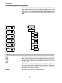
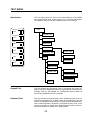
TABLE OF CONTENTS
CONDENSED INFORMATION
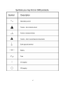
Safety and Preparation for Use
Symbols
Specifications
Quick Performance Check
Abridged Command List
INSTRUMENT OVERVIEW
SR430 Overview
Trigger and Sync/Busy
Bin Clock Output
Ext Bin Clk Input
Signal Input and Discriminator
Timing
Data Acquisition
Add, Subtract, Toggle, and Inhibit
Aux, Test, Disk, and Interfaces
RS232 Connector
Parallel Printer Connector
PC Keyboard Connector
BNC Connectors
3
4
5
8
9
MENUS
Levels Menu
Mode Menu
Display Menu
Setup Menu
Save Menu
Recall Menu
Math Menu
Plot Menu
Test Menu
Info Menu
11
11
12
12
12
13
13
13
14
OPERATION
Front Panel Overview
Power
Video Display
Soft Keys
Keypad
Spin Knob
Disk Drive
BNC Connectors
15
15
15
15
16
16
16
16
Screen Display
Data Display
Cursor Display
Menu Display
Data Acquisition Status
Status Indicators
17
17
18
18
18
19
Keypad
Normal and Alternate Keys
START and STOP/RESET
Menu Keys
Entry Keys
CURSOR
AUTOSCALE
PEAK
CENTER
NORM
PRINT
HELP
LOCAL23
21
21
21
22
22
22
22
23
23
23
23
23
Rear Panel
Power Entry Module
IEEE-488 Connector
25
25
25
INSTRUMENT SETUPS
Default Setup / Power On Clear
Choosing Bin Width & Record Length
Accumulation
Using the Trigger Offset
Using SYNC/BUSY76
REMOTE PROGRAMMING
GPIB Communications
RS232 Communications
Status Indicators and Queues
Command Syntax
Interface Ready and Status
1
25
25
26
26
27
29
35
37
47
53
59
67
69
73
75
76
76
76
79
79
79
79
80
Detailed Command List
Level Control Commands
Mode Control Commands
Display Control Commands
Setup Commands
Save and Recall Commands
Math Operation Commands
Print and Plot Commands
Data Acquisition Control Commands
Data Transfer Commands
Interface Control Commands
Status Reporting Commands
81
81
82
83
85
86
87
89
89
90
91
91
Status Byte Definitions
Serial Poll Status Byte
Standard Event Status Byte
MCS Status Byte
Error Status Byte
92
92
92
93
94
File Formats
Trace File
Settings File
Program Examples
IBM PC BASIC, RS232
Microsoft C, Nat'l Instruments GPIB
IBM PC BASIC, Nat'l Instruments
GPIB
95
95
97
97
99
101
TEST AND CALIBRATION
Power
Screen Brightness
Fan
Front Panel Tests
Power On Reset
Testing Data Acquisition Hardware
Counting Problems
Calibration
Signal Inputs
103
103
103
103
103
103
104
105
105
USING PHOTOMULTIPLIER TUBES
PMT Selection for Photon Counting
Geometry
Spectral Response
Gain and Risetime
Dark Counts
PMT Base Design
Dynode Biasing
Snubbing
Cathode Shielding
Magnetic Shielding
Preamplifiers
Gain Requirement
Plateauing a PMT
The 'Fast and Pretty Good' Way
107
107
107
107
107
108
108
109
110
110
110
111
111
111
TYPICAL EXPERIMENT
Energy Levels of Ruby
Apparatus
Operation
Instrument Configuration
Data Acquisition
113
113
113
114
114
CIRCUIT DESCRIPTION
Circuit Boards
Video Driver and CRT
CPU Board
Microprocessor System
Keypad Interface
Keyboard Interface
Spin Knob
Speaker
Clock/Calendar
115
116
116
116
116
116
117
117
117
Printer Interface
Video Graphics Interface
Disk Controller
GPIB Interface
RS232 Interface
Expansion Connector
117
117
117
117
117
117
Power Supply Board
Unregulated Power Supplies
Power Supply Regulators
118
118
118
ECL Logic Board
Signal Input
Discriminators
200 MHz Clock and Trigger Sync
Bin Clock Generator
Pulse Sorter
Counters
Shift Register Inputs
Control Signals
119
119
119
119
119
120
120
120
121
TTL Logic Board
Fast Record Buffers
Fast Buffer Address Counter
Accumulator
Copy Buffer Address Counter
Status and IO
Digital to Analog Converter
121
121
121
122
122
122
123
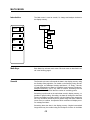
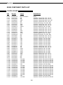
PARTS LISTS
Control Board
Power Supply Board
ECL Logic Board
TTL Logic Board
Hardware
Miscellaneous
125
125
129
132
138
142
144
ADDENDUM
145
SCHEMATIC DIAGRAMS
CPU Board
Power Supply Board
ECL Logic Board
TTL Logic Board
2
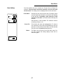
SAFETY AND PREPARATION FOR USE
WARNING: Dangerous voltages, capable of causing injury or death, are
present in this instrument. Use extreme caution whenever the instrument covers are removed. Do not remove the covers while the unit is
plugged into a live outlet.
CAUTION
protect against electrical shock. Always use an
outlet which has a properly connected protective
ground.
This instrument may be damaged if operated
with the LINE VOLTAGE SELECTOR set for the
wrong ac line voltage or if the wrong fuse is installed.
WARNING REGARDING USE WITH
PHOTOMULTIPLIERS
LINE VOLTAGE SELECTION
The signal inputs may be damaged if a photomultiplier is used improperly with the photon counter.
When left completely unterminated, a PMT will
charge a cable to a few hundred Volts in a very
short time. If this cable is connected to a signal input, the stored charge may damage the front-end
transistors. To avoid this problem, provide a leakage path of about 100 KΩ to ground inside the
base of the PMT to prevent charge accumulation.
The SR430 operates from a 100V, 120V, 220V, or
240V nominal ac power source having a line frequency of 50 or 60 Hz. Before connecting the power cord to a power source, verify that the LINE
VOLTAGE SELECTOR card, located in the rear
panel fuse holder, is set so that the correct ac input voltage value is visible.
CONNECTION TO OTHER INSTRUMENTS
Conversion to other ac input voltages requires a
change in the fuse holder voltage card position
and fuse value. Disconnect the power cord, open
the fuse holder cover door and rotate the fuse-pull
lever to remove the fuse. Remove the small printed circuit board and select the operating voltage
by orienting the printed circuit board to position the
desired voltage to be visible when pushed firmly
into its slot. Rotate the fuse-pull lever back into its
normal position and insert the correct fuse into the
fuse holder.
All front panel BNC shields are connected to the
chassis ground and to the power outlet ground via
the power cord. Do not apply any voltage to either
the shields or to the outputs. The outputs are not
protected against connection to any potential other
than ground.
FURNISHED ACCESSORIES
- Power Cord
- Operating Manual
LINE FUSE
ENVIRONMENTAL CONDITIONS
Verify that the correct line fuse is installed before
connecting the line cord. For 100V/120V, use a 1
Amp fuse and for 220V/240V, use a 1/2 Amp fuse.
OPERATING
Temperature: +10°C to +40°C
(Specifications apply over +18°C to +28°C)
Relative Humidity: <90% Non-condensing
LINE CORD
The SR430 has a detachable, three-wire power
cord for connection to the power source and to a
protective ground. The exposed metal parts of the
instrument are connected to the outlet ground to
NON-OPERATING
Temperature: -25°C to +65°C
Humidty: <95% Non-condensing
3
4
SR430 MULTICHANNEL SCALER / AVERAGER
GENERAL INFORMATION
The SR430 Multichannel Scaler / Averager counts incoming pulses in successive time bins. A trigger starts a
record of up to 32,704 time bins. The duration of the time bins is programmable from 5 ns to 10.5 ms. The
number of signal pulses counted during each time bin is stored in memory. There is no dead time between
bins. Each new trigger starts a record whose data is added to the bin by bin accumulation of all of the previous records. The result is a record of the sum (or average) of all counts in each time bin.
The trigger starts each record. The SYNC/BUSY output signals the beginning of the first time bin of the
record. The BIN CLOCK output signals the boundaries of each time bin. During each time bin, input signal
pulses are counted. At the end of the time bin, the counter data is stored in memory and the counter is reset.
The double buffered design ensures that there is no dead time between bins and no pulses are missed at the
bin boundaries.
After the record is complete, the data is added to the accumulation of all previous records. This only occurs
after the record of data is acquired and results in a accumulation dead time of 250 ns X number of bins in the
record (8 ms for 32k bins). After the accumulation is complete, the memory is re-armed for the next trigger.
The number of records accumulated is programmable 1 to 65,535 (or free run). The count capacity is 32,767
per bin per trigger. The total accumulation capacity per bin is also 32,767. The SYNC/BUSY output for each
record remains high from the trigger until the end of accumulation. When SYNC/BUSY returns low, another
trigger can be received.
The SR430 offers advanced functions such as Autoscale, Smoothing, Curve Fitting, non-volatile setup memories, data storage to disk, push button hardcopy to graphics printers and plotters, and GPIB and RS-232 interfaces. The SR430 is also easy to use. It has a menu based user interface which makes front-panel adjustments intuitive and straightforward. Entries are made with the front-panel knob or numeric keypad. On screen
help is available at all times.
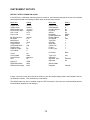
SPECIFICATIONS
SIGNAL INPUT
Bandwidth
Input impedance
Linear range
Input protection
Overload recovery
DISCRIMINATOR
Referred to the signal input:
Discriminator range
Resolution
Slope
Accuracy
Minimum pulse input amplitude
Pulse pair resolution
DISC view output
TRIGGER INPUT
Impedance
Threshold
Slope
dc to 250 MHz
50 Ω
±300 mV (at input)
±5 VDC, 50 V for 1 µs
5 ns for <10 µs duration overload
-300 mV to +300 mV
0.2 mV
Positive or Negative
2 mV + 1%
10 mV
10 ns (typical)
NIM level into 50 Ω
There is a 20 ns insertion delay from signal input to discriminator output.
10 kΩ
-2.000 V to +2.000 V in 1 mV steps
Rising or Falling
5
SR430 Multichannel Scaler
Protection
INTERNAL TIME BINS
Bin width
Accuracy
Jitter (rms)
Indeterminacy
Insertion delay
EXTERNALLY CLOCKED TIME BINS
EXT BIN CLK Input
Maximum frequency
Minimum pulse width high
Minimum pulse width low
Insertion delay
COUNTERS/ACCUMULATION
Bins per record
Maximum count rate
Maximum count
Records per accumulation
Maximum accumulation
Add/Subtract
TRIGGER RATE
Minimum period between triggers
OUTPUTS
DISC
SYNC/BUSY
BIN CLK OUTPUT
TOGGLE
TEST
AUX1, AUX2
15 VDC, 100 V for 1 µs
5 ns, 40 ns, 80 ns, 160 ns, 320 ns, 640 ns, 1.28 µs, 2.56 µs, ...
10.486 ms. (10 ns or 20 ns bins are not available)
1 ns + 20 ppm of bin width
100 ps + 10 ppm of delay from SYNC/BUSY output (Time bins are
synchronous with the SYNC/BUSY output).
2.5 ns pk-pk with respect to the TRIGGER input
45 ns from trigger to first bin. Rising edge of SYNC/BUSY output occurs at the beginning of the first bin. However, signal pulses arriving
25 ns after the trigger will be counted in the first bin.
Rising edge triggers next time bin.
4 MHz (250 ns minimum bin width)
100 ns
100 ns
Rising edge of SYNC/BUSY output occurs at first rising edge of EXT
BIN CLK after TRIGGER. The beginning of the first bin occurs at the
same time. (Time bins are synchronous with the SYNC/BUSY output).
1k to 16k in 1k increments (1024 to 32,704 including Trigger Offset)
100 MHz
32,767 per bin per trigger
1 to 64k (or free run)
32,767 per bin in Add mode, ±16,383 per bin in Toggle, or External
mode.
Records may be added or added an subtracted (Toggle between add
and subtract every N triggers where N is programmable). External
subtract input may also control the toggle.
Tp=Record time + Accumulation time + Overhead
=(Number of Bins X Bin Width)+(Number of Bins X 250 ns)+150
µs
SYNC/BUSY output is high for Tp after each trigger. When
SYNC/BUSY returns low, the next record may be triggered. Triggers
received while SYNC/BUSY is high are ignored.
Nim level into 50 Ω. Low whenever the signal input exceeds the discriminator level with the correct slope.
TTL level. Rising edge is synchronous with the first time bin of each
record. Use this edge to trigger the experiment. Remains high until
re-armed for next trigger.
Nim level into 50 Ω. Each transition is a bin boundary. Active only
while a record is being acquired. Timing skew relative to the DISC
output is less than 2 ns.
TTL level. Indicates whether the next record will be added to or subtracted from the accumulation. (Internal toggle mode)
50 MHz Nim output into 50 Ω. Use to test counters.
General purpose analog outputs
Full scale
±10 VDC
Resolution
12 bits (5 mV)
6
SR430 Multichannel Scaler
Output current rating
Output impedance
Accuracy
INPUTS
SIGNAL
TRIGGER
BIN CLK INPUT
ACCUMULATOR INHIBIT
SUBTRACT
GENERAL
Interfaces
Hardcopy
Disk
Power
Dimensions
Weight
Warranty
10 mA
<1 Ω
0.1% + 10 mV
Analog 50 Ω input.
10 kΩ input.
TTL input. Rising edge triggers next time bin
TTL input, sampled each trigger. If high, causes the current record to
be ignored (not accumulated)
TTL input, sampled each trigger. If high, causes the current record to
be subtracted from the accumulation ( in external toggle mode).
IEEE-488 , RS-232, and Centronics Printer standard. All instrument
functions can be controlled and read through the IEEE-488 and RS232 interfaces.
Screen dumps to Epson compatible dot matrix or HP LaserJet printers (parallel). Plots to HPGL compatible plotters (serial or IEEE-488).
3.5" MSDOS compatible format, 720kbyte capacity. Storage of data
and setups.
60 Watts, 100/120/220/240 VAC, 50/60 Hz
17"W X 6.25"H X 16.5"L
30 lbs
One year parts and labor on materials and workmanship
7
SR430 Multichannel Scaler
SR430 Quick Performance Check
Be sure to read the Overview and Operations sections of the manual to familiarize yourself with the instrument.
This setup requires a 1 Hz to 2 kHz TTL trigger source. A simple function generator will suffice.
Hold down the CLR key while turning the unit on. This resets the SR430 to its default state.
Connect the trigger source to the TRIGGER input on the front panel. Set the Trigger Level and Slope in the
LEVELS menu appropriately for the trigger source. Use a 5 foot length or longer BNC cable to connect the
TEST output on the rear panel to the SIGNAL input on the front panel. Set the Disc Level to -300 mV and the
Disc Slope to Falling.
Set the trigger rate to 1 kHz. Press the START key. Data acquisition should begin. The default bin width is 5
ns and the record length is 1k. 1000 records will be accumulated. When the scan is done, press AUTOSCALE
to scale the display. The TEST output is a 50 MHz signal so a pulse occurs every 20 ns or every 4 bins. The
data should have 1000 counts in every 4th bin.
Use the Mode menu to select different bin widths and records per scan. Records with longer bin widths trigger
at lower rates so the trigger rate needs to be lowered to avoid RATE errors. Use the formula for Tbusy in the
Specifications section of the manual to calculate the maximum trigger rate for each bin width and record
length. Longer bin widths also require a smaller number of records per scan to avoid overflow. This is because each bin acquires a larger number of counts per trigger.
Bin widths of 40 ns and longer will collect data in every bin. The first bin may have 1 less count per trigger
than the other bins. For longer bin widths 163 µs or longer, the data may vary up to ±7 counts per bin per trigger. This is due to the jitter in the longer bin widths.
After acquiring data, use the other menus to scale the data, smooth or perform calculations with the data,
save and recall data to disk, etc.
8
SR430 Multichannel Scaler
COMMAND LIST
LEVELS
TRLV(?) {x}
TRSL(?) {i}
DCLV(?) {x}
DCSL(?) {i}
AUX1(?) {x}
AUX2(?) {x}
Set the Trigger Level to -2.000 <= x <= 2.000 V.
Set the Trigger Slope to Positive (0) or Negative (1).
Set the Discriminator Level to -0.3000 <= x <= 0.3000 V.
Set the Discriminator Slope to Positive (0) or Negative (1).
Set the AUX1 Level to -10.000 <= x <= 10.000 V.
Set the AUX2 Level to -10.000 <= x <= 10.000 V.
MODE
BCLK(?) {i}
BWTH(?) {i}
BREC(?) {i}
RSCN(?) {i}
BOFF(?) {i}
ACMD(?) {i}
TCNT(?) {i}
PTOG(?) {i}
REAC
ROFF(?) {i}
Set the Bin Clock Source to Internal (0) or External (1).
Set the internal Bin Width to 5 ns (0) through 10.486 ms (19).
Set the number of Bins Per Record to 1 ≤ i ≤ 16 times 1024.
Set the number of Records Per Scan to 0 ≤ i ≤ 65535.
Set the Trigger Offset to 0 ≤ i ≤ 16320 in increments of 16.
Set the Accumulate Mode to Add (0), Toggle (1), or External (2).
Set the Toggle Count to 1 ≤ i ≤ 16384.
Set the Pause At Toggle mode Off (0) or On (1).
ReAcquire count data from data acquisition memory.
Set the ReAcquire From Offset to 0 ≤ i ≤ Trigger Offset in increments of 16.
DISPLAY
AUTS
CRPK
BUGP?
CNTR
LEFT(?) {i}
BOTM(?) {i} {x}
HSCL(?) {i}
VSCL(?) {i} {x}
CURS(?) {i}
CURW(?) {i}
CURM(?) {i}
GRID(?) {i}
AutoScale the graph. Same as [AUTOSCALE] key.
Move the cursor to the on screen peak. Same as [PEAK] key.
Query the Cursor Marker bin number.
Translate the graph to center the cursor. Same as [CENTER] key.
Set the Left edge of the graph to bin #i.
Set the Bottom of the graph to i counts or x value.
Set the Horizontal Screen Width to 8 bins (0) through 16k bins (22).
Set the Vertical Scale to i counts/division or x/division in a 1-2-5-10 sequence.
Turn the Cursor Off (0) or On (1).
Set the Cursor Width to Normal (0), Wide (1), or Spot (2).
Set the Cursor Seek Mode to Maximum (0), Minimum (1), or Mean (2).
Turn the Grid Off (0) or On (1).
SETUP
OUTP(?) {i}
KCLK(?) {i}
ALRM(?) {i}
THRS(?) {i}
TMIN(?) {i}
TSEC(?) {i}
DMTH(?) {i}
DDAY(?) {i}
DYRS(?) {i}
PLTM(?) {i}
PLTB(?) {i}
PLTA(?) {i}
PLTS(?) {i}
PNTR(?) {i}
PNGD(?) {i}
PNAP(?) {i}
PNCR(?) {i}
PNFT(?) {i}
PRNT(?) {i}
Set the Output Interface to RS232 (0) or GPIB (1).
Turn the Key Click Off (0) or On (1).
Turn the Alarms Off (0) or On (1).
Set the Hours to 0 ≤ i ≤ 23.
Set the Minutes to 0 ≤ i ≤ 59.
Set the Seconds to 0 ≤ i ≤ 59.
Set the Month to 1 ≤ i ≤ 12.
Set the Day to 1 ≤ i ≤ 31.
Set the Year to 0 ≤ i ≤ 99.
Set the Plotter Mode to RS232 (0) or GPIB (1).
Set the Plotter Baud Rate to 300 (0), 1200 (1), 2400 (2), 4800 (3), 9600 (4).
Set the Plotter GPIB Address to 0 ≤ i ≤ 30.
Set the Plot Speed to Fast (0) or Slow (1).
Set the Trace Pen Number to 1 ≤ i ≤ 6.
Set the Grid Pen Number to 1 ≤ i ≤ 6.
Set the Alphanumeric Pen Number to 1 ≤ i ≤ 6.
Set the Cursor Pen Number to 1 ≤ i ≤ 6.
Set the Fit Pen Number to 1 ≤ i ≤ 6.
Set the Printer Type to Epson (0) or HP (1).
SAVE AND RECALL
FNAM(?) {string}
Set the current
File Name to
9
SR430 Multichannel Scaler
string.
SVTR
SVST
SVSS
RCTR
RCST
RCSS
Save the Trace Data to the file specified by FNAM.
Save the Settings to the file specified by FNAM.
Save the System Configuration to the file specified by FNAM.
Recall the Trace Data from the file specified by FNAM.
Recall the Settings from the file specified by FNAM.
Recall the System Configuration from the file specified by FNAM.
MATH
SMTH i
FTYP(?) {i}
FITS
PARS? i
LLIM(?) {i}
RLIM(?) {i}
CALC
ARGT(?) {i}
ARGM(?) {i}
STAT
SPAR? i
Smooth the data using 5 pts (0), 11 pts (1), 17 pts (2), 21 pts (3), or 25 pts (4).
Set the Fit Type to Line (0), Exponential (1), or Gaussian (2).
Start the Fit Calculation.
Query Fit Parameter t0 (0), a (1), b (2), or c (3).
Set the Left Limit of the curve fit region to bin #i where 0 ≤ i < Right Limit.
Set the Right Limit of the curve fit region to bin #i where Left Limit < i ≤ Last bin in record.
Start a Calculation
Set the calculation Argument type to Constant (0), or File (1).
Set the Constant Argument to x.
Start the Statistical Calculations.
Query Statistical Parameter mean (0), deviation (1), area (2), baseline area (3).
PRINT AND PLOT
PRSC
Print the screen. Same as [PRINT] key.
PALL
Plot the entire screen.
PTRC
Plot the trace only.
PCUR
Plot the cursor only.
DATA ACQUISITION CONTROL
SSCN
Start data acquisition. Same as [START] key.
PAUS
Pause a scan in progress. Same as [STOP] key while BUSY.
CLRS
Reset the data memory. Same as [STOP] key while DONE.
SCAN?
Query the number of records which have been accumulated so far.
DATA TRANSFER
BINA? {i}
Read the entire data record in ASCII format. If i included, read only bin #i data.
BINB?
Read the entire data record in binary format.
INTERFACE
*RST
*IDN?
LOCL(?) {i}
Reset the unit to its default configurations.
Read the SR430 device identification string.
Set the Local/Remote state to LOCAL (0), REMOTE (1), or LOCAL LOCKOUT (2).
STATUS
*CLS
*ESE(?) {i}
*ESR? {i}
*SRE(?) {i}
*STB? {i}
*PSC(?) {i}
ERRE(?) {i}
ERRS? {i}
MCSE(?) {i}
MCSS? {i}
Clear all status registers.
Set the Standard Status Byte Enable Register to the decimal value i (0-255).
Query the value of the Standard Status Byte. If i is included, only bit i is queried.
Set the Serial Poll Enable Register to the decimal value i (0-255).
Query the value of the Serial Poll Status Byte. If i is included, only bit i is queried.
Set the value of the Power-On Status Clear bit to Set (1) or Clear (0).
Set the Error Status Enable Register to the decimal value i (0-255).
Query the value of the Error Status Byte. If i is included, only bit i is queried.
Set the MCS Status Enable Register to the decimal value i (0-255).
Query the value of the MCS Status Byte. If i is included, only bit i is queried.
10
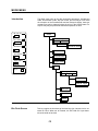
INSTRUMENT OVERVIEW
record can only acquire 4 counts per bin maximum
(4 * 10 ns = 40 ns). If the bins width is 5 ns, then
the maximum number of counts per bin is 1. The
maximum count capacity of each bin is 32,767.
When the bin width is large and the count rate is
high, it is possible to exceed the count capacity of
a bin in a single record. In this case, the data will
overflow and be stored as the maximum count
(32,767).
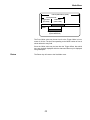
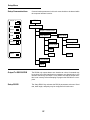
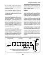
SR430 OVERVIEW
The SR430 data acquisition timing is diagrammed
below. A trigger starts a record of up to 32,704
time bins (T 1, T2, ... T N). Each time bin is of equal
duration and is programmable from 5 ns to 10 ms.
There is no dead time between time bins. During
each time bin, signal pulses are counted. At the
end of each time bin, the counter data is stored in
memory. The memory address is then incremented and the counter is reset for the next time bin.
Thus, a record is a list of counter data points corresponding to counts received in successive time
bins. Counts which arrive at a bin boundary are
not missed but either fall in the bin just ending or
in the bin just starting.
A single record can capture a transient counting
signal if there are enough counts to be statistically
significant in a single shot. If the count rate is very
low but the signal is repetitive, then multiple
records may be accumulated. Accumulation of
records means simply taking each new record and
adding it to the sum of all previous records on a
bin by bin basis, i.e. data from T1 of each record is
summed together, data from T2 of each record is
summed together, etc. Accumulation reduces statistical noise since the accumulated counts in each
bin will be larger than the data from a single
record. Each bin can accumulate counts up to
32,767. Additional counts will cause an overflow
and the data will be stored as 32,767. If this limit is
reached, then the bin width should be reduced and
the bins per record increased (to keep the same
record time). This will divide the bins which overflowed, into 2 or more smaller bins, each capable
of 32,767 counts. Thus, more total counts may be
accumulated for the same record time.
The number of bins per record is set in 1k increments from 1k (1024) to 16k (16,384). This represents the maximum number of bins which can be
displayed and analyzed at one time. This limitation
is due to the data display buffer having a maximum capacity of 16k data points. The data acquisition memory, however, can store up to 32k data
points. Up to 32,704 bins may actually be acquired
and accumulated, of which, up to 16k bins may be
displayed at a time. The Trigger Offset determines
how many bins are skipped at the beginning of the
total record before data is transferred to the display buffer.
The maximum count rate is 100 MHz or one count
every 10 ns. Thus, short bins can only acquire a
small number of counts per bin in a single record.
For example, if the bin width is 40 ns, then a single
A scan is an accumulation of a number of records.
The number of records in a scan may be programmed from 1 to 65,535.
TRIG
45 ns
SYNC/
BUSY
BIN CLK
TBUSY
T
1
T
2
T
3
ACCUMULATION AND
PROCESSING TIME
T
N
BIN WIDTH
SIGNAL
INPUT
20 ns
DISC
OUT
TIMING DIAGRAM
11
Instrument Overview
SYNC/BUSY is only output during actual data acquisition. Triggers that arrive when the unit is not
acquiring data will not cause a SYNC/BUSY output.
TRIGGER and SYNC/BUSY
Data acquisition is started by a trigger. The TRIGGER input is on the front panel. The trigger threshold is adjustable from -2V to +2V and the slope
may be either RISE or FALL.
BIN CLOCK OUTPUT
The front panel BIN CLK output is a 50 ½, NIM level signal showing the bin boundaries. The first
bin,T1, is the time period when the BIN CLK is
first low following a trigger. Each rising and falling
transition of the BIN CLK marks the boundary of a
bin. Thus, the second bin, T2, is when BIN CLK is
next high, T3 is when BIN CLK is low again, etc.
The SYNC/BUSY output is a TTL level signal
which serves two purposes. First, it can be used to
synchronize the experiment timing with the actual
time bins of each record. Second, it indicates
when the unit is busy acquiring data and cannot
be triggered.
After a trigger is recognized, the SYNC/BUSY output will go high indicating the start of the first time
bin. The insertion delay from TRIGGER to SYNC/
BUSY is 45 ns. SYNC/BUSY will have 2.5 ns of indeterminacy with respect to the trigger. As a result, the entire record starts with 2.5 ns of uncertainty with respect to the trigger. This is not a
problem if the bin width is much longer than 2.5 ns
but may be a problem for shorter bin widths. In
these cases, the SYNC/BUSY output should be
used to trigger the experiment. Since the record is
synchronized to SYNC/BUSY, there will be no indeterminacy of the time bins with respect to the
experiment. One way to accomplish this is to trigger the SR430 with the experiment's master rate
generator and use the SYNC/BUSY (which is delayed from trigger by only 45 ns) to trigger the actual experiment.
The first bin starts synchronously with the SYNC/
BUSY output. BIN CLK may be used with the
DISC OUT signal to determine the exact timing of
the counts with respect to the time bins.
BIN CLK is only output during actual data acquisition. Triggers that arrive when the unit is not acquiring data will not cause a BIN CLK output.
EXT BIN CLK INPUT
The front panel EXT BIN CLK input is a TTL input
which allows an external source to determine the
bin boundaries. When the bin width mode is programmed to EXTERNAL, the EXT BIN CLK will
clock the bins. After a trigger, the first rising edge
of the EXT BIN CLK will start the first bin. SYNC/
BUSY goes high at the same time. Each new rising edge of the EXT BIN CLK will clock the start of
a new bin. The maximum external clock rate is 4
MHz or a 250 ns minimum external bin width. The
EXT BIN CLK is useful if bins longer than 10.5 ms
are required, or when the bins must be synchronized to external events.
After a trigger, the unit is busy acquiring and accumulating data. During this busy time, no new triggers will be recognized. After SYNC/BUSY returns
low, a new trigger may occur. The busy time is
Tbusy = (N*Tbin) + (N*250 ns) + 150 µs
SIGNAL INPUT AND DISCRIMINATOR
where Tbin is the bin width (5 ns to 10.5 ms) and
N is the number of bins per record (1024 to
32704). The first term is the actual record length
and equals the real time duration of the data acquisition. Counts received during the time N¥Tbin
after the trigger are captured. The second term is
the time needed to accumulate the record, i.e. add
the data to the sum of all previous data. Accumulation takes 250 ns per bin. The last term is a fixed
overhead for processing. For example, if N=1k
bins and Tbin = 5 ns, then Tbusy = 411 µs. The
maximum trigger rate would then be 2400 Hz.
When the bin width is programmed to be much
larger than 250 ns, then the busy time is almost totally due to the real time data acquisition and virtually no time is lost processing or accumulating.
The analog signal input is labelled SIGNAL INPUT
on the front panel. This input is internally terminated into 50 ½. The input can accept signals of either polarity up to ±300 mV and is protected to
±5V dc. The input is followed by a dc to 250 MHz
amplifier. This allows detection of pulses as small
as 10 mV. If greater sensitivity is required, the
SR440 remote pre-amplifier can be used. The
SR440 can provide gains from 5 to 125 at bandwidths exceeding 200 MHz.
Following the input amplifier is a discriminator.
The discriminator has selectable slope and a
threshold programmable from -300 mV to +300
mV in 0.2 mV steps (referred to the inputs). Pulsepair resolution is 10 ns and pulses of either
12
Instrument Overview
polarity may be detected.
ber of time bins in a single record. Each trigger will
take N data points corresponding to N sequential
time bins. N may be programmed from1024 to
32704 (including Trigger Offset).
The discriminator output is labelled DISC OUT on
the front panel. The DISC OUT is a 50 ½, NIM level signal showing the actual input to the counter.
The output is active low (-0.7 V) and counting occurs on the falling edge. The output is low when
the signal input exceeds the threshold level with
the correct slope, i.e. the signal is higher than the
threshold with positive slope or the signal is lower
than the threshold with negative slope.The DISC
outputs are very useful when adjusting discriminator thresholds or determining the exact timing of
the counts relative to the time bins.
Records are accumulated until the number of
records per scan, R, have been acquired. R may
be programmed from 1 to 65536. If R is set to 0
(free run), then accumulation continues without
end. This mode is convenient when timing an experiment since BIN CLK and SYNC/BUSY are output only when data is being acquired. When R is
0, every trigger will output SYNC/BUSY and BIN
CLK without stopping after a programmed number
of triggers.
The DISC OUT is active at all times. Whenever a
signal pulse exceeds threshold with the correct
slope, a pulse is output at DISC OUT. The unit
does not have to be actively acquiring data. This
enables setting the discriminator threshold without
triggering the unit.
After the record length and scan length have been
programmed, data acquisition can be started.
When the [START] key is pressed or a START
command is received from the computer interface,
data acquisition begins. The next TRIGGER will
start the first record and count data will be stored.
TIMING
Successive triggers will acquire records which are
accumulated until the number of records per scan
have been taken. During this time, the unit is
BUSY and the SYNC/BUSY and BIN CLK outputs
are active. After the number of records per scan
have been accumulated, data acquisition is halted.
The unit is now in the DONE state. Triggers which
arrive while the unit is DONE are ignored and
SYNC/BUSY and BIN CLK are inactive.
The DISC OUT signal is delayed internally by 20
ns so that the DISC OUT and the BIN CLK output
are correct relative to each other. In other words, a
DISC OUT pulse which falls in the first BIN CLK
will be counted in the first bin. However, a DISC
OUT pulse is actually due to a signal pulse arriving
20 ns earlier at the SIGNAL INPUT. This means
that BIN CLK and DISC OUT, when viewed on a
scope using equal length cables terminated into
50 ½, are accurately timed. However, for timing
purposes, each output viewed by itself is 20 ns
late relative to the trigger. Since the insertion delay
for the BIN CLK is 45 ns, signal pulses arriving 25
ns after the trigger will be output at the DISC OUT
45 ns after the trigger and counted in the first bin.
For accurate timing, it is best to use DISC OUT
and BIN CLK, rather than SIGNAL INPUT and BIN
CLK since the latter pair are skewed by 20 ns.
When the data acquisition is DONE, the final accumulated data is displayed on the screen and may
be analyzed and manipulated. Before taking data
again, the current data must be cleared by pressing the [STOP/RESET] key or sending the RESET
command via the computer interface. This will
clear the count memory and the display. The unit
will now be in the CLEAR state. While in the
CLEAR state, the data acquisition setup may be
altered. A new record length or bin width may be
programmed, etc. The [START] key will start data
acquisition once again and put the unit in the
BUSY state.
Thus, even though the BIN CLK is output with a 45
ns insertion delay relative to the TRIGGER, the actual insertion delay is 25 ns (20 ns less). Signal
pulses arriving 25 ns after the TRIGGER will be
counted.
ADD, SUBTRACT, TOGGLE, and INHIBIT
Normally, records are accumulated by summing
corresponding bin data from successive records.
Records may also be subtracted from the accumulation. The accumulation mode may be set to
ADD, SUBTRACT, TOGGLE, or EXTERNAL.
Note that SYNC/BUSY and BIN CLK are only output only during actual data acquisition while the
DISC OUT is active all of the time.
DATA ACQUISITION
ADD will sum new records to the accumulation.
SUBTRACT will subtract new records from the accumulation.
To begin acquiring data, the number of bins per
record and the number of records per scan must
be programmed. The record length, N, is the num-
13
Instrument Overview
TOGGLE will switch between ADD and SUBTRACT every M records where M is programmable. In this mode, the rear panel TOGGLE OUTPUT will be TTL high before the trigger of those
records which will be subtracted.
ed directly connected to the RS232 or GPIB interface. Data will be plotted directly from the SR430
without a computer.
EXTERNAL will subtract records whenever the external SUBTRACT INPUT is TTL high. The SUBTRACT INPUT is sampled at the trigger and will
determine whether that record will be added or
subtracted.
A parallel printer port is standard on the SR430.
Any EPSON compatible dot matrix graphics printer
or HP LaserJet printer may be used. Full screen
printouts may be generated by pressing the
[PRINT] key on the front panel.
The rear panel INHIBIT INPUT is used to ignore a
record. If INHIBIT is TTL high when the trigger is
received, that record is ignored and not accumulated. The record does count towards the number of
records accumulated.
KEYBOARD
PRINTER
An IBM PC compatible keyboard may connected
to the keyboard connector. The keyboard must operate in the PC or XT mode. This is often called
the 8088 mode. The keyboard may be used to enter data instead of the keypad. This is most useful
with disk file names.
AUX 1, AUX 2
The rear panel AUX 1 and AUX 2 outputs are programmable general purpose dc analog outputs.
The output voltages may be set from the front panel or computer interface and can range from -10V
to +10V. These outputs may be used wherever an
external variable dc voltage is required
TEST
The rear panel TEST output is a 50Ω, NIM level
output. The output frequency is 50 MHz and is
synchronous with the BIN CLK. The TEST output
is used to test that the counter and accumulator
are working properly. By connecting the TEST output to the SIGNAL input, a known number of
counts can be put into every time bin. This allows
the user to quickly check the functionality of the
unit.
DISK DRIVE
The 3.5" disk drive is used to save data, setups,
and configurations. The format is DOS compatible
and the capacity is 720k.
COMPUTER INTERFACES
RS232 and GPIB (IEEE-488) interfaces are standard on the SR430. All settings of the instrument
may be controlled via the computer interfaces.
Data may also be transmitted to a computer.
PLOTTING
An HPGL compatible plotter may also be connect-
14
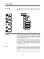
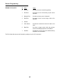
GUIDE TO OPERATION
Brightness Control
Power Button
FRONT PANEL OVERVIEW
Soft Keys
Spin Knob
Key Pad
Disk Drive
Front Panel BNC Connectors
Video Display
POWER BUTTON
The SR430 is turned on by pushing in the POWER
button. The video display may take a few seconds
to warm up and become visible. Adjust the brightness until the screen is easily readable.The model,
firmware version, and serial number of the unit will
be displayed briefly when the power is turned on.
The memory status is also displayed. All instrument settings are stored in nonvolatile memory
and are retained when the power is turned off. If
the memory check passes, then the instrument returns to the settings in effect when the power was
last turned off. If there is a memory error, then the
stored settings are lost and the default settings are
used. To reset the unit into the default state, hold
down the [CLR] key while the power is turned on.
The default setup is listed in a later chapter.
The main area of the display is occupied by the
data display. Data is graphed as accumulated
counts per bin on the vertical axis and bin # or
time from trigger on the horizontal axis. The graph
is continuously updated during data acquisition.
When data acquisition is DONE, the total accumulated data is displayed.
A complete description of the screen display follows in the next section.
SOFT KEYS
The SR430 has a menu driven user interface. The
6 soft keys to the right of the video display have
different functions depending upon the information
displayed in the menu boxes at the right of the video display. In general, the soft keys have two
uses. The first is to toggle a feature on and off or
to choose between 2 settings. The second is to
highlight a parameter which is then changed using
the spin knob or numeric keypad. In both cases,
the soft keys affect the parameters which are displayed adjacent to them.
VIDEO DISPLAY
The monochrome video display is the user interface for data display and front panel programming
operations. The resolution of the display is 640H
by 480V. The brightness is adjusted using the
brightness control knob located at the upper left
corner. As with most video displays, do not set the
brightness higher than necessary. The display
may be adjusted left and right using the Setup
Screen function in the SETUP menu.
15
Guide To Operation
KEYPAD
BNC CONNECTORS
The keypad consists of four groups of keys. The
ENTRY keys are used to enter numeric parameters which have been highlighted by a soft key.
The MENU keys select a menu of soft keys.
Pressing a menu key will change the menu boxes
which are displayed next to the soft keys. Each
menu groups together similar parameters and
functions. The CONTROL keys start and stop actual data acquisition, select the cursor and autoscale the display. These keys are not in a menu
since they are used frequently and while displaying any menu. The SYSTEM keys print the screen
to a printer and display help messages. Once
again, these keys can be accessed from any
menu.
TRIGGER
The rising or falling edge of the TRIGGER input
triggers a record. The input impedance is 10 KΩ
and the minimum pulse width is 10 ns. The trigger
level is adjustable from -2V to +2V with either
slope. The minimum pulse amplitude is 100 mV.
SYNC/BUSY
TTL output high whenever the SR430 is acquiring
or accumulating a record. Triggers received during
this time are ignored. The rising edge of SYNC/
BUSY is synchronous with the start of the first bin
and may be used to trigger the experiment to remove the 2.5 ns uncertainty between trigger and
SYNC/BUSY. This output is active only when the
SR430 is in the BUSY state actively accumulating
records.
A complete description of the keys follows in the
next section.
SIGNAL INPUT
The SIGNAL INPUT is a 50 Ω analog input. A photomultiplier or preamplifier output is connected to
this input. The input is linear between -300 mV to
+300 mV and protected to ± 5 Vdc.
SPIN KNOB
The spin knob is used to adjust parameters which
have been highlighted using the soft keys. Any numeric entry field may be adjusted using the knob.
In addition, functions such as display zooming and
scrolling use the knob as well. In these cases, the
knob function is selected by the soft keys. The
[CURSOR] key, which can be pressed at any time,
will set the knob function to scrolling the cursor.
DISC OUT
The DISC output is a 50 Ω, NIM level output is active low (-0.7 V) when the signal input exceeds the
threshold level with the correct slope. Counting occurs on the falling edge.
DISK DRIVE
BIN CLK OUT
The BIN CLK output is a 50 Ω, NIM level output
showing the position of the time bins. Each transition of this output is a bin boundary. This output is
active only when SYNC/BUSY is active.
The 3.5" disk drive is used to store data and instrument settings. Double sided, double density disks
should be used. The disk capacity is 720k bytes
formatted. The disk format is DOS compatible.
Disks written by the SR430 may be read by PC
compatible computers equipped with a 3.5" drive
and DOS 3.0 or higher.
EXT BIN CLK INPUT
The EXT BIN CLK is a TTL input whose rising
edges mark the bin boundaries. The maximum
clock rate is 4 MHZ. This input is active if the bin
width has been programmed to EXTERNAL.
OPTION
This connector is unused.
16
Guide To Operation
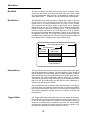
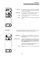
SCREEN DISPLAY
Data Acquisition
status (CLR, BUSY,
PAUSE, or DONE).
Cursor Position and data
value. When surrounded by a
box, indicates that the knob
will move the cursor region.
Soft Key Definitions. Pressing the
corresponding soft key will either
highlight a field or select an option.
Soft Keys
bin 71
727.0 µsec
Y = 50 cnts
SRS DONE
Cursor Marker is
located at the Min,
Max, or Mean of the
data within the
cursor region.
Trigger Level
500 mV
Trigger Slope
Disc. Level
-10.0 mV
Cursor Region is
defined by these
dashed lines.
Disc. Slope
Aux. 1 Level
0.0 V
Left most
displayed bin and
time.
bin 0
0 msec
bottom = 0 cnts
Minimum displayed Y value.
This Y value corresponds to
the bottom of the graph.
bin 127
1.300 msec
Record = 100
10 cnts/Div
Aux. 2 Level
0.0 V
Number of records
accumulated so far.
Vertical scale.
R i g h t most displayed
bin and time.
DATA DISPLAY
Data is graphed with accumulated counts per bin
on the Y axis and bin number or time on the X
axis. The physical size of the graph remains constant while the vertical and horizontal scales may
be changed. The graph area has a dotted grid for
reference. There are 8 vertical divisions and 10
horizontal divisions. In addition to X and Y scaling,
the graph may also be translated in the X and Y directions.
across the graph. If the number of bins displayed
is less than the 496, then each data point is shown
as a horizontal line at the correct Y position. The
graph above shows data in this mode. When the
number of bins exceeds 496, then each X screen
location on the graph corresponds to multiple bins.
The data is then displayed as a vertical line at
each X screen location. The displayed line connects the maximum and minimum values of the
data points at each X screen location.
Data is shown in 2 modes depending upon the X
scaling. There are 496 pixels or X screen locations
The Left most displayed bin and time is the X value corresponding to the left edge of the graph.
17
Guide To Operation
scaling, each X screen location may represent
multiple data points. The cursor marker can still
seek the min, max, or mean of the data at a single
X screen location.
The Right most displayed bin and time is the X
value of the right edge of the graph. These values
represent the X scale and translation. The X scale
is (Right-Left)/10 per division. The horizontal scale
ranges from 16 bins to N bins across the graph.
The actual position of the displayed data within the
record is given by the Left and Right values. Bin
#0 is the first bin in the record and Bin #N-1 is the
last bin where N is the programmed number of
bins per record. The Left and Right values mark
the region of the record displayed on the graph.
The graph may be horizontally translated in increments of 1/100 of the screen or 1 bin, whichever is
larger.
The Cursor Position displays the X position (bin
# and time) and the Y data of the cursor marker. In
the case where each X screen location represents
multiple data points, the actual bin# corresponding
to the min, max, or mean is displayed. Pressing
the [CURSOR] key will draw a box around the cursor information. When the cursor readout is surrounded by a box, the spin knob is to adjusts the
position of the cursor region. The cursor region
moves in increments of one X screen location or
pixel.
The Vertical scale is the number of accumulated
counts per division displayed on the graph. This
value is changed whenever the vertical scale is
adjusted. The vertical scale ranges from 1 to 5000
counts per division. The Minimum displayed Y
value corresponds to the Y value of the bottom
edge of the graph. This value is changed whenever the graph is translated up or down. The graph
may be translated in the vertical direction in increments of 1/80 of the screen or 1 count, whichever
is larger.
MENU DISPLAY
The Soft Key menu boxes define the functions of
the 6 soft keys at the right of the screen. The
menu boxes are grouped into menus. Pressing
each of the ten menu keys will display a different
menu of boxes. Related functions are grouped into
a single menu. In general, pressing a soft key
does one of two things. One is to toggle between 2
or 3 choices directly. An example is the Trigger
Slope box illustrated on the previous page. Pressing the second soft key toggles the slope between
rising and falling. The second soft key function is
to highlight an entry field and knob function. An example would be the Trigger Level. Pressing the
first soft key will highlight the Trigger Level value.
The Trigger Level may then be adjusted with the
knob or programmed with a value using the numeric entry keys. Each menu is described at
length in a following section.
The Number of Records accumulated is displayed in the bottom right corner. While data is being acquired and accumulated, the graph is being
constantly updated to display the data accumulated so far. Each time the data is updated, the number of records is updated. When the scan is complete, the graph will show the total accumulated
data and the number of records accumulated will
be equal to the programmed number of records
per scan. While data acquisition is in progress, the
graph shows the data accumulated and the number of records completed.
DATA ACQUISITION STATUS
CURSOR DISPLAY
The Data Acquisition status is displayed in the
upper left corner. The acquisition status is always
displayed and is always in inverse video. CLR indicates that the accumulation memory and counters
are reset. The data are all zeroes. All parameters
can be changed while in the CLR state. Pressing
the [START] key will start data acquisition and the
status will change to BUSY. While in the BUSY
state, data is graphed as it accumulates and parameters related to the data acquisition may not
be changed. When the programmed number of
records per scan has accumulated, then data acquisition is DONE. The graph will show the final
accumulation. Acquisition may be paused during
BUSY by pressing the [STOP] key. The status is
then PAUSE. While in the PAUSE state, the
[START] key continues data acquisition and the
[STOP] key will reset to the CLR state. In general,
pressing the [STOP] key twice in succession will
The Cursor Region is the graph region between
the vertical dashed lines. The cursor region may
be set to 1 division (wide), 1/2 division (norm), or a
single vertical line (spot). The cursor region does
not change with horizontal scaling. The Cursor
Marker is a small square which seeks the minimum, maximum, or mean of the data within the
cursor region. When seeking min or max, the cursor marker is located at the position of the data
point which is the min or max. This allows peaks
and valleys in the data to be easily read out. When
seeking the mean, the X position of the cursor
marker is at the center of the cursor region and the
Y position is the mean of the data within the region. When a spot cursor region is used, the cursor marker is confined to a single X screen location. However, depending upon the horizontal
18
Guide To Operation
reset to the CLR state.
SUB, TOGGLE, or EXTERNAL accumulate
mode). The overflowed bin(s) will stay at the limiting value while non-overflowed bins continue to
accumulate normally.
STATUS INDICATORS
In addition to the acquisition status, there are a
number of other status indicators which may be
displayed. These indicators are visible only when
the condition they represent is present. The position of these indicators is fixed, they simply turn on
and off. The indicators are shown below.
ERR
Flashes whenever there is a computer interface
error such as illegal command or out of range parameter is received. This does not flash for a printer or plotter error.
ALT
Indicates that the ALTERNATE keypad is in use.
The ALTERNATE keypad uses the alphabetic legends printed below each key. The [ENTER] key
has the same function in the ALTERNATE keypad.
To enter the ALT mode, press the [ALT] key once.
Pressing the keys will now enter alphabetic characters into the active entry field. To return to the
normal keypad, press the [ALT] key again.
SRS
DONE Trigd RATE ERR SRQ
ALT Add OFLW Act REM
Act
Flashes when there is activity on the computer interfaces. This does not flash for printer or plotter
activity.
SRQ
This indicator turns on when a GPIB Service Request is generated by the SR430. SRQ stays on
until a serial poll of the SR430 is completed.
REM
bin 71This indicator
727.0 isµsec
on when
the frontLevel
panel is locked
Trigger
by a computer interface. No front panel adjustY = 50out
cnts
500
mV the unit to local
ments may be made. To
return
control (if allowed), press the [HELP] key.
Trigd
Flashes on whenever a record is triggered during
data acquisition. Trigd does not flash unless the
unit is in the BUSY state (after the [START] key is
pressed). Triggers received during other times will
not flash this indicator.
Trigger Slope
Disc. Level
Add or Sub
This indicates whether the next record will be added to or subtracted from the accumulation. Sub is
may be active if the accumulation mode is set to
SUB, TOGGLE, or EXTERNAL.
-10.0 mV
Disc. Slope
RATE
This flashes when a trigger is received while
SYNC/BUSY is high, i.e. the unit is still acquiring
data from a previous trigger. These triggers are ignored and do not contribute to the data accumulation. The extra triggers simply flash the RATE indicator. Only triggers received while SYNC/BUSY is
low will trigger a data record.
Aux. 1 Level
0.0 V
bin 127
1.300 msec
Record = 100
bin 0
OFLW
0 msec
This
indicator will turn on during accumulation if
cnts/Div
bottom
= 0 cnts more than 10
any
bin accumulates
32,767
counts (in
ADD accumulate mode) or ±16,384 counts (in
19
Aux. 2 Level
0.0 V
Guide To Operation
20
Guide To Operation
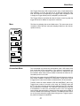
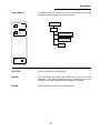
KEYPAD
CONTROL
START
STOP
RESET
+
SYSTEM
CURSOR
-
AUTO
SCALE
/
8
A
4
5
1
0
S
ALT
O
T
Y
L
MATH
RECALL
R
PLOT
W
TEST
X
INFO
=
Z
SETUP
Q
V
ENTER
F
K
P
U
CLR
DISPLAY
SAVE
EXP
--
MODE
E
J
NORM
3
•
D
I
N
LEVELS
CENTER
6
2
M
PEAK
C
H
G
)
MENU
9
B
(
*
ENTRY
7
HELP
PRINT
\
state are ignored and SYNC/BUSY and BIN CLK
OUT are inactive.
NORMAL AND ALTERNATE KEYS
The normal key definitions are printed on each
key. In addition, each key also has an alternate
definition printed below it. The [ALT] key toggles
the keypad between the two definitions. The ALT
screen indicator is on when the alternate definitions are in use. The [ALT] and [ENTER] keys
have the same definition in both modes. The alternate keys should only be used when accessing
files on the disk drive.
[START] begins the data acquisition. The first trigger after [START] is pressed will trigger the first
data record. The data acquisition status will switch
to BUSY. Successive triggers will acquire records
which are accumulated. While the unit is BUSY,
the SYNC/BUSY and BIN CLK outputs are active
and accumulated data is graphed on the display.
Each successful trigger will generate a SYNC/
BUSY pulse and a BIN CLK pulse train. Triggers
received during SYNC/BUSY active times are ignored. After the programmed number of records
have been accumulated, data acquisition is halted.
The unit is now in the DONE data acquisition
state. The final accumulated data is now graphed
on the display. Further triggers will be ignored and
SYNC/BUSY and BIN CLK OUT are inactive.
Pressing the [STOP] key while in the BUSY state
pauses the data acquisition. The data acquisition
status will be PAUSE and no triggers will be recognized. Pressing [START] will continue the data ac-
START, STOP, AND RESET
The [START] and [STOP/RESET] keys are used
to start, pause, and reset the counter and accumulation memory.
Data acquisition can be started only if the counters
and memory are in the CLEAR or reset condition;
all data values are zero. The CLEAR condition is
indicated by the CLR data acquisition status indicator. Triggers which arrive while in the CLEAR
21
Guide To Operation
quisition and pressing [STOP] will reset the unit to
the CLEAR state.
A new trigger level may now be entered using the
numeric keys. For example, to set the level to
-0.125, press [-] [1] [2] [5] [EXP] [-] [3] or [-] [.] [1]
[2] [5] or any combination of keys which evaluates
to the correct value. Note that entry is done in
units of Volts. The entry field will display the characters as the keys are pressed. If an error is
made, the backspace [<-] key will erase the last
character and [CLR] will restore the field to the
original value. When the entry string is correct,
Pressing [STOP] while in the PAUSE or DONE
states will reset the unit to the CLEAR condition.
All data accumulated will be lost and reset to zero.
In general, pressing the [STOP] key twice in succession will put the unit in the CLEAR condition.
IMPORTANT NOTE: Data which is cleared cannot be recovered! Be sure to save valuable
data to the disk to avoid accidentally erasing it.
SRS
DONE
MENU KEYS
bin 71
727.0 µsec
Y = 50 cnts
All operating parameters of the SR430 are
grouped into ten function menus. The ten menu
keys select which menu of parameters is displayed next to the six soft keys. The soft keys then
either toggle a parameter, highlight a parameter
entry field (for numeric entry or knob adjustment),
or display a submenu.
The [LEVELS] menu displays the trigger, discriminator, and auxiliary D/A levels. The [MODE] menu
displays the bin width, bins per record, records per
scan, accumulation mode, and trigger offset. The
[DISPLAY] menu shows graph translation and
zoom and the cursor modes. The [SETUP] menu
configures the computer interfaces, sound, real
time clock, plotter, and printer. The [SAVE] and
[RECALL] menus are the disk menus. Data, settings ([LEVELS] and [MODE]), and system setups
may be saved and recalled from disk. The [MATH]
menu analyzes and manipulates data. Smoothing,
curve fitting, statistical analysis, and calculations
may be performed on the data. The [PLOT] menu
is used to plot the data graph on a plotter. The
[TEST] menu allows the user to test the keypad,
external keyboard, knob, RS232 interface, printer
interface, disk drive, video screen, and memory.
The [INFO] menu displays various information
screens.
bin 0
0 msec
bottom = 0 cnts
10 cnts/Div
Trigger Level
500 mV
Trigger Slope
press the [ENTER] key to change the trigger level
to the new value. If another soft key is used to
highlight a different parameter field or to toggle a
Disc. Level
setting, or the [CURSOR]
key is pressed to highlight the cursor field, or a new menu key is
pressed, before [ENTER] is pressed, the displayed
entry will be cleared and the original value restored.
-10.0 mV
Disc. Slope
Whenever a parameter entry field is highlighted,
the knob may also be used to adjust the value. If
the knob is turned during numeric entry before the
[ENTER] key has been pressed, the value will be
adjusted starting from the original value.
Aux. 1 Level
CURSOR
0.0 V
Pressing the [CURSOR] key highlights the cursor
information field by drawing a box around it. The
bin will
127
knob
now scroll
cursor region. The [CURAux. the
2 Level
SOR]msec
key highlights the cursor field in the same
1.300
0.0would
V
way =that
a soft key
highlight a parameter
Record
100
field. The highlighted cursor field appears below.
Detailed descriptions of each menu are provided
in the next section.
Any previously highlighted parameter field will become non-highlighted and any entry in progress is
cancelled. Pressing a soft key to highlight a parameter field will let the knob adjust the new parameter while the cursor will become de-selected.
ENTRY KEYS
The numeric entry keys are used to enter parameter values directly. Parameters may be entered
only if their menu box is displayed and their entry
field is highlighted. For example, if the LEVELS
menus is displayed, the first soft key is next to the
Trigger Level box. Pressing the first soft key will
highlight the entry field displaying the trigger level.
The menu box will appear as illustrated below.
AUTOSCALE
Pressing [AUTOSCALE] will automatically set the
vertical scale and translation to display the entire
range of the data. The graph will also be translat-
22
Guide To Operation
bin 71
727.0 µsec
Y = 50 cnts
Trigger Level
500 mV
Trigger
Slope
ed so that the it is centered. [AUTOSCALE]
does
not affect the horizontal scaling or translation.
While autoscaling is taking place, the message
"AutoScaling" will appear just below the graph. If
the number of bins being displayed is very large,
the autoscale operation may take a noticeable
Disc. Level
amount of time.
-10.0 mV
[AUTOSCALE] may be pressed at any time during
or after data acquisition. While the unit is BUSY
accumulating and updating the graph, [AUTODisc. Slope
SCALE] may be used to periodically re-scale
the
graph as the data accumulates beyond the top of
the graph.
[AUTOSCALE] only operates on the data which is
displayed on the graph. Data corresponding
to
Aux. 1 Level
bins which are not shown do not figure in the autoscaling calculations.
0.0 V
PEAK
bin 127 Aux. 2 Level
Pressing [PEAK] will center the cursor
region
around the maximum1.300
data msec
value on the screen.
0.0 V
10 cnts/DivThe cursor markerRecord
= 100
will be positioned
at the Min,
Max, or Mean of the data within the region, depending upon the cursor mode. The [PEAK] key
only searches the data which is on the screen. If
the maximum value occurs at more than one location, then [PEAK] will find the one closest to the
left edge.
the description of the MATH menu for more information about floating point representations of the
data. Data may be restored to the original count
data using the [REACQUIRE] function in the
MODE menu.
[NORM] is useful when measuring relative quantities such as absorption or gain.
PRINT
[PRINT] will print the currently displayed screen to
a printer attached to the rear panel parallel printer
port. The entire screen, including text and menus,
is printed. The time and date will also be printed.
The printer type needs to be configured in the
SETUP menu before using [PRINT]. A "PrScrn in
Progress" message will appear on the screen
while printing is in progress. No other front panel
operations may be performed until printing is completed. If no printer is attached or there is a printer
error, then the print operation is aborted after
about 10 seconds. A "PrScrn Aborted" message
will appear briefly on the screen.
HELP
[HELP] provides on screen help with any key or
soft key. Pressing [HELP] followed by any key will
display information about the function or use of
that key. [HELP] with a soft key will describe the
menu item next to the soft key. Pressing another
key will exit the help screen.
The [PRINT] key is the one key for which no help
is available. Pressing [PRINT] at any time will print
the screen, including the help screens.
LOCAL
CENTER
When a host computer places the unit in the REMOTE state, no keyboard or knob input is allowed.
To return to front panel operation, press the
[HELP] key.
The [CENTER] key will horizontally translate the
graph to place the bin corresponding to the cursor
marker at the center of the graph. The horizontal
scale is not affected. If the translation can only be
accomplished by displaying bins prior to bin #0 or
after the last bin, then no action is taken. This can
occur when trying to center a bin which is within
half of the horizontal scale of either end of the
record.
NORM
[NORM] will normalize the entire record of data to
the data value of the cursor marker, i.e. all data
values are divided by the cursor marker data value. The new value of the cursor marker data is
1.000. The new data will no longer be counts per
bin but will simply be floating point numbers. See
23
Guide To Operation
24
Guide To Operation
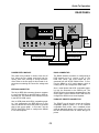
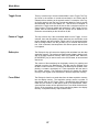
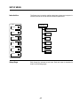
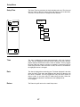
REAR PANEL
Power
Entry
Module
Rear Panel BNC Connectors
PC Keyboard Connector
IEEE-488 (GPIB) Connector
RS232 Connector
Parallel Printer Connector
POWER ENTRY MODULE
RS232 CONNECTOR
The power entry module is used to fuse the AC
line, select the line voltage, and block high frequency noise from entering or exiting the instrument. Refer to the first page of this manual for instructions on selecting the correct line voltage and
fuse.
The RS232 interface connector is configured as a
DCE (transmit on pin 3, receive on pin 2). The
baud rate, parity, and word length are programmed from the SETUP RS232 menu. To connect the SR430 to a PC serial adapter, which is
usually a DTE, use a straight thru serial cable.
IEEE-488 CONNECTOR
Also, a serial plotter with HPGL compatible graphics may be connected to the RS232 port. The
SR430 will drive the plotter to generate plots of the
screen graph. Use the SETUP PLOTTER menu to
configure the SR430 to use a serial plotter.
The 24 pin IEEE-488 connector allows a computer
to control the SR430 via the IEEE-488 or GPIB instrument bus. The address of the instrument is set
in the SETUP GPIB menu.
PARALLEL PRINTER CONNECTOR
Also, a GPIB plotter with HPGL compatible graphics may connected to the IEEE-488 port. In this
case, the SR430 will control the plotter to generate
plots of the screen graph. In this case, use the
SETUP PLOTTER menu to configure the SR430
to use a GPIB plotter.
The [PRINT] key will print the screen to an Epson
compatible graphics printer or an HP LaserJet
compatible laser printer. Use a standard printer
cable to attach the printer to the printer port. Use
the SETUP PRINTER menu to choose the type of
printer.
25
Guide To Operation
what the accumulation mode of the next record will
be. This output is only used if the accumulation
mode is set to TOGGLE. TOGGLE switches at the
end of the SYNC/BUSY time to reflect the accumulation mode of the next trigger. If TOGGLE is
high, then the next record will be subtracted. The
state of TOGGLE at the time of the trigger determines the accumulation mode of the data record.
PC KEYBOARD CONNECTOR
A n IBM PC or XT compatible keyboard may be attached to the keyboard connector. An AT keyboard may be used if it can be switched to PC or
8088 mode. Typing at the attached keyboard is
the same as entering numbers and letters from the
front panel keypad. Highlighted parameter entry
fields will accept characters from the keyboard.
Typing 'E' or 'e' is the same as [EXP]. In general,
the keyboard is only useful for alphabetic fields
such as file names.
TEST
TEST is a 50 Ω, NIM level output. The output frequency is 50 MHz and is synchronous with the
BIN CLK. The TEST signal is used to test the
counter and accumulator by putting a known number of counts into each bin. See the Test and
Troubleshooting section for further information.
BNC CONNECTORS
INHIBIT INPUT
If the INHIBIT input is TTL high when a trigger is
received, then that record of data is ignored and
not accumulated. The record will count towards
the number of records per scan.
AUX 1 and AUX 2
The AUX outputs are general purpose programmable dc analog outputs. The output voltages may
be set from the LEVELS menu. The output range
is -10V to +10V and the maximum current output
is 10 mA.
SUBTRACT INPUT
When the accumulate mode is set to EXTERNAL,
records which are triggered when the SUBTRACT
INPUT is TTL high are subtracted from the accumulation. This input is sampled at the trigger to determine what to do with the ensuing data record.
TOGGLE OUT
The TOGGLE OUT is a TTL signal which indicates
26
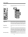
LEVELS MENU
Introduction
Trigger Level
The Levels menu is used to set the trigger and discriminator settings as
well as the Aux output levels.
LEVELS
500 mV
Trigger Level
Trigger Slope
Trigger Slope
Disc. Level
Discriminator Level
-10.0 mV
Disc. Slope
Discriminator Slope
Aux 1 Level
Aux. 1 Level
0.0 V
Aux 2 Level
Aux. 2 Level
0.0 V
Trigger Level
Pressing the Trigger Level key selects the trigger threshold level as the
active entry field. A new trigger level may be entered from the numeric
keypad (in units of Volts) or the knob may be used to adjust the present
level. The trigger threshold is adjustable from -2.000V to +2.000V with
1mV resolution. The minimum pulse amplitude required to trigger is 0.1V.
Trigger Slope
The Trigger Slope key changes the trigger slope to either rising or falling
edge.
Discriminator Level
The Discriminator Level key selects the discriminator threshold as the active entry field. A new threshold level may be entered from the numeric
keypad (in units of Volts) or the knob may be used to adjust the level.
The discriminator threshold is adjustable from -300mV to +300mV with
0.2mV resolution. The minimum signal pulse amplitude required is 10
mV. The Disc. Out signal is the output of the discriminator. Viewing this
signal on an oscilloscope while adjusting the threshold can be helpful in
determining the appropriate level. See the "Using Photomultipler Tubes"
section later in this manual.
The Discriminator Slope key changes the discriminator slope to either rising or falling edge. If the input signal pulses are negative going, then the
Discriminator Slope
27
Levels Menu
slope should be set to falling. If the signal pulses are positive going, then
slope should be rising. In either case, the Disc. Output is always active
low; i.e., a discriminated rising edge of the signal will be output as a negative going NIM pulse at the Disc. Output. The falling edges of the Disc.
Output are counted.
Aux 1 Level
The Aux 1 Level key selects the output level of the AUX 1 output as the
active entry field. A new output level may be entered from the numeric
keypad (in units of Volts) or the knob may be used to adjust the present
level. The output level is adjustable from -10.000V to +10.000V with 5mV
resolution.
Aux 2 Level
The Aux 2 Level key selects the output level of the AUX 2 output as the
active entry field. A new output level may be entered from the numeric
keypad (in units of Volts) or the knob may be used to adjust the present
level. The output level is adjustable from -10.000V to +10.000V with 5mV
resolution.
28
MODE MENU
Introduction
Bin Clk Src
Internal
External
The Mode menu sets up the data acquisition parameters, including bin
width, accumulation mode, bins per record, and records per scan. With
the exception of the Records/Scan and the ReAcquire Offset, these parameters may not be changed unless the unit is in the CLEAR state. ReAcquire may only be performed when data acquisition is done.
MODE
Bin Clock Source
Internal
External
Bin Width
20.48 µs
Internal Bin Width
Bins/Record
1k
Bins/Record
Records/Scan
Records/Scan
1000
Trigger Offset
Trigger Offset
0
0.00 µsec
More
More:
Accumulate Mode
Add Toggle Ext
Toggle Count
Pause at Toggle
ReAcquire
From Offset
Return
Bin Clock Source
This key toggles the time base of the time bins from internal clock to external bin clock. When set to External, the EXT BIN CLK input determines the width of each bin.
29
Mode Menu
Bin Width
This key is activated only when the Bin Clock Source is Internal. Pressing this key will activate the internal bin width entry field. The bin width
may only be adjusted using the knob. The available bin widths are 5ns,
40ns, 80ns,160 ns, ... , 10.486ms. 10ns and 20ns bins are not available.
Bins/Record
The Bins/Record key allows the knob to change the number of bins per
record. Numeric entry is not allowed in this field. The number of bins per
record is set in 1k (1024) increments from 1k (1024) to 16k (16,384).
This represents the maximum number of bins which can be displayed
and analyzed at one time. This limitation is due to the data display buffer
having a maximum capacity of 16k data points. The data acquisition
memory, however, can store up to 32,704 data points. Up to 32,704 bins
may actually be acquired and accumulated, of which, up to 16k bins may
be displayed at one time. The Trigger Offset determines how many bins
are skipped at the beginning of the total record before data is transferred
to the display buffer. A simple memory map is shown below.
Data Acquisition Memory (32704)
Total Acquired Data
Trigger Offset
(0 to 16320)
Bins/Record
(1024 to 16384)
Display Memory
(equal to Bins/Record)
Records/Scan
This key activates the Records per Scan entry field. Both numeric entry
and knob adjustment are allowed. The Records/Scan is the number of
records which will be accumulated before the data acquisition is DONE.
The Records/Scan may be programmed from 0 to 65,535. When set to 0,
accumulation will continue indefinitely until the [STOP] key is pressed.
This mode of operation is useful when setting up an experiment since the
BIN CLK OUT and SYNC/BUSY out will both be active indefinitely instead of only until the scan is DONE.
The Records/Scan may be changed while data acquisition is in progress.
If the new value is less than the present number of records accumulated,
the scan will finish with the next record. If the new value is greater, then
accumulation progresses normally until the new number of records has
been acquired.
Trigger Offset
The Trigger Offset determines how many bins are skipped at the beginning of the total record before data is transferred to the display buffer. Up
to 32,704 bins may actually be acquired and accumulated, but only a
maximum of 16k bins may be displayed at one time. The actual number
of bins which are stored in the data acquisition memory is equal to Trigger Offset plus Bins/Record with a maximum of 32,704.
30
Mode Menu
The Trigger Offset entry field accepts numeric entry or knob adjustments.
The resolution is 16 bins and the limit is 16,320 bins. Below the entry
field, the actual time corresponding to the trigger offset is displayed. This
is simply the Trigger Offset (in bins) multiplied by the bin width.
The Trigger Offset is used when the data of interest occurs long after the
trigger and short bin widths are required for resolution.
More
The More key displays the second Mode menu. This menu sets the accumulation mode and also reacquires displayed data from the data acquisition memory.
Accumulate
Add Toggle
Ext
Toggle Cnt.
1
Pause at Toggle
Yes
No
ReAcquire:
From Offset
0
0.00 µsec
Return:
Accumulate Mode
The Accumulate key selects the accumulation mode. ADD mode sums
new record data to the accumulation. The maximum accumulation per
bin is 32,767. EXT and TOGGLE can either add to or subtract from the
accumulation. When either of these modes is selected, the maximum accumulation per bin is ±16,383.
EXTernal mode means that the SUBTRACT input will determine whether
each record is added or subtracted. If SUBTRACT is high when a record
is triggered, then that record's data is subtracted from the accumulation.
TOGGLE mode will switch between ADD and SUBTRACT after every
Toggle Count number of records. In this mode, the TOGGLE output will
be TTL high when the next record is to be subtracted and TTL low when
the next record is to be added. The TOGGLE output switches at the end
of SYNC/BUSY to reflect the accumulate mode of the next triggered
record. When data acquisition is started, the first toggle count number of
records is added before switching to subtract. The Add/Sub status indicator on the screen shows the toggle status during a scan. Toggle is generally used for background subtraction.
31
Mode Menu
Toggle Count
This key is active only if the Accumulate Mode is set to Toggle. The Toggle Count is the number of records accumulated in one mode (add or
subtract) before switching to the opposite mode. For example, if the Toggle Count equals 4, then the first 4 records are added, the next 4 records
are subtracted, the next 4 are added, etc. , until the scan is complete. In
general, the Toggle count should be set so that a complete scan has an
equal number of records added and subtracted. If the Toggle Count is
greater than the Records/Scan, then all records will be added but the
maximum accumulation per bin will still be 16,383.
Pause at Toggle
This key is active only if the Accumulate Mode is set to Toggle. If Yes is
selected, then data acquisition pauses whenever the accumulate mode
toggles between add and subtract. This is useful if the experiment takes
time to change modes. Use the [START] key to continue data acquisition. If No is selected, data acquisition runs without pause until the scan
is completed.
ReAcquire
The ReAcquire key will restore the display buffer with data from the data
acquisition memory. The total accumulated record of data is always available in the data acquisition memory while in the DONE state. When the
[STOP/RESET] key is used to reset to the CLEAR state, all accumulated
data is lost.
The number of bins transferred to the display memory for graphing and
analysis is equal to the Bins/Record. This data may be changed using
the MATH menu functions. For example, the data may be squared, multiplied by a constant, normalized, etc. These operations alter the data in
the display memory. The ReAcquire function will restore the display
memory to the original count data stored in the data acquisition memory.
From Offset
The ReAcquire function re-reads data from the data acquisition memory
into the display memory. The acquisition memory stores a number of
data points equal to the Trigger Offset + Bins/Record while ReAcquire
reads only the number of data points equal to the Bins/Record. ReAcquire skips the number of bins specified in the From Offset field at the beginning of the acquisition memory before transferring data to the display
memory. A simplified memory map is shown below.
32
Mode Menu
Data Acquisition Memory (32704)
Total Acquired Data
Trigger Offset
(0 to 16320)
Bins/Record
(1024 to 16384)
From
Offset
ReAcquired Display Memory
(equal to Bins/Record)
The From Offset value may be set from 0 to the Trigger Offset in increments of 16 bins. The time corresponding to the Offset number of bins is
shown below the entry field.
Since the Offset value may be less than the Trigger Offset, bins which
were not originally displayed while the data was taken may be displayed
using ReAcquire.
Return
The Return key will return to the first Mode menu.
33
Mode Menu
34
DISPLAY MENU
Introduction
Translate
The Display menu is used to change the graph parameters and cursor
mode. Note that cursor movement is activated by the [CURSOR] key and
not by this menu.
DISPLAY
Translate
Zoom
Zoom
Cursor
On
Cursor On/Off
Off
Cursor Width
Norm Wide
Spot
Cursor Width
Cursor Seeks
Cursor Seeks
Max Min
Mean
Grid On/Off
Grid
On
Off
Translate
The Translate key will activate knob control of graph translation in either
the vertical or horizontal direction. When the Translate key is pressed,
the currently selected direction will become highlighted, and the knob will
now translate the graph in that direction. Pressing the Translate key
again will toggle to the other axis.
Horizontal translation is in increments or 1/100 of the screen width rounded up to the nearest integer number of bins. Translation below bin #0 or
past the last bin is not allowed.Vertical translation is in increments of 1/10
of a division or 1 count whichever is larger. If the data is in floating point
representation (as a result of a Math function), then translation is in increments of 1/10 of a division.
Zoom
The Zoom key will activate knob control of graph scaling in either the vertical or horizontal direction. When the Zoom key is pressed, the currently
selected direction will become highlighted , and the knob will now expand
the graph in that axis. Pressing the Zoom key again will toggle to the other axis.
Vertical scaling is in a 1-2-5-10 sequence starting with 1 count/division
35
Display Menu
and going up to 5000 counts/division (40000 counts full scale). This allows the full range of count data to be displayed. If the data is in floating
point representation (as a result of a Math function), zooming in is limited
by the 16 bit resolution of the data. Vertical zooming takes place about
the cursor marker (if the cursor is on) or the center of the screen (if the
cursor is off).
Horizontal scaling is in powers of 2 from 8 bins up to 1k bins across the
screen, and above 1k bins in increments of 1k up to the number Bins/
Record (1k to 16k) across the full screen. Horizontal zooming takes place
about the cursor marker position unless the cursor is too close to the beginning or end of the record. In this case, zooming will leave the left or
right edge of the graph unchanged.
Cursor On/Off
This function turns the cursor region and cursor marker on and off. It is
sometimes desirable to turn off the cursor before printing the screen.
Cursor Width
This function selects the width of the cursor region defined by the vertical
dashed lines on the graph.
Normal width is 1/2 of a division, Wide is 1 division, and Spot is a single
X position on the screen (the cursor marker is a single dashed line).
The cursor region moves to the left and to the right a single pixel at a
time. There are 496 pixels across the graph.
Cursor Seeks
The cursor marker searches the data points within the cursor region for
the maximum or minimum data value, or calculates the mean of the region. This key toggles between Max, Min, and Mean.
When seeking minimum or maximum, the cursor marker is located at the
minimum or maximum data point. This allows peaks and valleys in the
data to be read easily. When seeking mean, the X position of the cursor
marker is the center of the cursor region and the Y position is the mean
of the data within the region. When a spot cursor region is used, the cursor marker is confined to a single X screen location. However, depending
upon the horizontal scaling, each X screen location may represent multiple data points. The cursor marker can still seek the minimum, maximum,
or mean of the data at a single X screen location.
Grid On/Off
This function turns the grid display on and off. The grid is the set of dotted lines on the graph which mark each scale division.
36
SETUP MENU
Introduction
Setup
The Setup menu is used to configure the printer, plotter and computer interfaces, and set the sound and clock/calendar parameters.
SETUP
Commun.
Communications
Setup
Sound
Sound
Setup
Time
Time
Setup
Plotter
Plotter
Printer
Setup
Printer
Screen
Setup
Screen
Setup Keys
Each Setup Key activates a sub menu. Each sub menu is described in
detail in the following pages.
37
Setup Menu
Setup Communications
Output To
RS-232
Communication parameters in this sub menu should not be altered while
the computer interface is active.
SETUP
GPIB
Setup
Communications
RS232:
Output To Rs232/GPIB
Setup
GPIB:
Setup RS232
View
Setup GPIB
Baud Rate
GPIB Address
Word Length
Overide Remote ?
Queues:
Parity
Return
Return:
Return
View Queues
Return
Output To RS232/GPIB
The SR430 only outputs data to one interface at a time. Commands may
be received over both interfaces but responses are directed only to the
interface selected by the Output To key. Make sure that the Output interface is set correctly before attempting to program the SR430 from a computer.
Setup RS232
The Setup RS232 key activates the RS232 parameters sub menu. Baud
rate, word length, and parity may be configured in this sub menu.
38
Setup Menu
Baud Rate
9600 bd
Baud Rate
The Baud Rate key allows the knob to adjust the RS232
baud rate. The baud rate can be set to any standard value from 300 to 19200 baud.
Word Length
This key toggles the character length. The RS232 character length can be 7 or 8 bits. 8 bits is standard.
Parity
This key toggles the parity. The RS232 parity can be
Even, Odd, or None.
Return
The Return key will return to the Setup Communications
menu.
Word Length
7 bits
8 bits
Parity
Even
Odd
None
Return:
Setup GPIB
The Setup GPIB key activates the GPIB parameters sub menu. GPIB instrument address and Remote Overide are set in this sub menu.
GPIB Address
8
GPIB Address
This key activates the GPIB Address entry field for numeric and knob entry. The instrument address can be
set from 0 to 30.
Overide Remote ?
In general, every GPIB interface command will put the
SR430 into the REMOTE state with the front panel inactivated. To defeat this feature, set the Overide Remote ?
to Yes. In this mode, no GPIB remote enable will put the
unit into REMOTE state.
Overide Remote?
Yes
No
If the SR430 is in the REMOTE state, the [HELP] key returns the unit to local front panel control.
Return
The Return key will return to the Setup Communications
menu.
Return:
39
Setup Menu
View Queues
The last 256 characters received or transmitted by the SR430 may be
displayed to help find programming errors. The View Queues key will display the interface buffers as they are when the key is pressed. This
screen is updated regularly to display new interface activity. The View
Queues screen may slow down the communications between the SR430
and a host computer. In general, the View Queues screen should be displayed only when testing or debugging a host program.
The most recent data is displayed at the right of the upper line of each
queue display. For example, in the screen below, the DCLV?[lf] string
was the most recently received command. The [lf] character is a line-feed
and is the string delimiter. The most recently transmitted string is
.010000[lf] in response to the DCLV? command. The earliest command
received was *IDN? and the earliest response was "Stanford Research
Systems,SR430,s/n00001,ver007"[lf]. Unrecognized characters are ignored and not displayed. The terminator character on the output queue is
always shown as a [lf]. When the output is directed to the RS232 interface, a carriage return [cr] is actually sent in place of the [lf].
Press any key (except [PRINT]) to restore the screen to the graph mode.
Return
The Return key will return to the main Setup menu.
SRS
CLR
bin 71
727.0 µsec
Y = 50 cnts
Receive Queue:
Output To
RS-232 GPIB
Setup
*IDN? TRLV? DCLV?
RS232:
Setup
GPIB:
Transmit Queue:
View
rch_Systems,SR430,s/n00001,ver007 0.100000 .010000
Queues:
Stanford_Resea
Press Any Key to Continue
bin 0
0 msec
bottom = 0 cnts
10 cnts/Div
40
bin 127
1.300 msec
Record = 100
Return:
Setup Menu
Setup Sound
Key Click
On
SETUP
Off
Sound
Alarms
On
The Setup Sound key activates the sound sub menu. Key click and
alarms are enabled and disabled in this sub menu.
Off
Key Click On/Off
Alarms On/Off
Return
Return:
Key Click
This key turns the key click on and off.
Alarms
This key enables and disables the audible alarms. Alarms will sound
whenever a front panel programming error or interface error occurs.
Alarms are also used to draw the user's attention to a message.
Return
The Return key will return to the main Setup menu.
41
Setup Menu
Setup Time
Time
The Setup Time key activates the clock/calendar sub menu.The time and
date are used to label all screen prints and plots as well as disk files.
This menu is used to check or change the time and date.
SETUP
09 : 10 : 23
Date
Time
10 / 31 / 89
Time
Date
Return
Return:
Time
The time is displayed as hours:minutes:seconds. A 24 hour format is
used. The time displayed is the time when the Setup Time menu was displayed and does not advance until the menu is redrawn. This key toggles
the entry field from hours to minutes to seconds. A new entry may be
made using the knob. When the knob is used, the clock is set whenever
the highlighted value is changed.
Date
The date is displayed as month:day:year. The date displayed is the date
when the Setup Time menu was displayed and does not advance until
the menu is redrawn. This key toggles the entry field from months to
days to years. A new entry may be made using the knob. When the
knob is used, the calendar is set whenever the highlighted value is changed.
Return
The Return key will return to the main Setup menu.
42
Setup Menu
Setup Plotter
The Setup Plotter sub menu configures the SR430 plotter driver. Interface, plot speed, and pen definitions are set in this sub menu. To actually
start plotting, use the [PLOT] key to select the Plot menu.
Plot Mode
RS-232
SETUP
GPIB
Plotter
Baud Rate
9600 bd
Plot Mode
RS232
Plot Speed
Fast
GPIB
Slow
Baud Rate
Plotter Address
Define
Pens:
Plot Speed
Define Pens
Trace Pen
Return:
Grid Pen
Alpha Pen
Cursor Pen
Fit Pen
Return
Return
Plot Mode
The SR430 can drive either an RS232 or GPIB interface plotter. The plotter must be HP-GL compatible. This function selects which interface to
use. The plotter connects to the RS232 or GPIB connector on the rear
panel.
Plot Mode
RS-232
GPIB
Baud Rate
Baud Rate
9600 bd
Plotter Addr.
If the Plot Mode is RS232, then the Baud Rate for the plotter may be selected. The baud rate is adjusted using the knob and must match the
baud rate of the plotter.
If the Plot Mode is GPIB, then the Plotter Address must be set. The Plot-
Plot Speed
Define
Pens:
43
Setup
Menu
Plot Mode
RS-232
GPIB
Plotter Addr.
ter Address may be entered from the keypad or by using the knob. The
Plotter Address must agree with the address of the plotter in use.
1
Plot Speed
Plot Speed
Define
This key toggles the Plot Speed. Normally, when plotting on paper, the
Fast Plot Speed is used. When plotting on transparencies or other nonstandard media, the Slow plot speed may be better.
Pens:
Define Pens
Many plotters have a multipen carousel. In this case, each part of the
screen may be plotted using a different color pen. The Define Pens key
activates a sub menu in which each feature of the screen may be assigned a pen number. The allowable pen numbers are from 1 to 6. When
using a single pen plotter, all features are plotted using the one pen regardless of the pen definitions.
Return:
Trace Pen
1
Grid Pen
Trace Pen
Grid Pen
This field assigns a pen number to the data trace on the
screen.
This field assigns a pen number to the graph grid.
1
Alpha Pen
This field assigns a pen number to all of the alphanumeric characters on the screen.
Cursor Pen
This field assigns a pen number to the dashed cursor region lines and cursor marker.
Fit Pen
This field assigns a pen number to any curve fit which
may
be
drawn
on
the
screen.
Return
This key returns to the Setup Plotter menu.
Alpha Pen
1
Cursor Pen
1
Fit Pen
1
Return:
Return
The Return key will return to the main Setup menu.
44
Setup Menu
Setup Printer
Printer Type
Epson
The Setup Printer menu is used to select the type of printer attached to
the parallel printer port. The [PRINT] key prints the screen to the printer.
SETUP
HP
Printer
Printer Type
Return
Return:
Printer Type
This function toggles the Printer Type between Epson and HP. Epson is
used for any Epson compatible graphics dot matrix printer and HP is
used for an HP LaserJet laser printer or compatible.
Return
The Return key will return to the main Setup menu.
45
Setup Menu
Setup Screen
The Setup Screen menu is used to adjust the position of the display on
the screen. The display area may be moved left and right.
Move
SETUP
Right:
Screen
Move
Left:
Move Right
Move Left
Return
Return:
Move Right
This function moves the display to the right on the screen.
Move Left
This function moves the display to the left on the screen.
Return
The Return key will return to the main Setup menu.
46
SAVE MENU
Introduction
Save
The Save menu is used to save data and parameters to disk. The Disk
Utilities menu can erase files and format blank disks. Files are saved as
DOS files and can be read by a DOS compatible computer with a 3.5"
disk drive. The file format is described in the Remote Programming section.
SAVE
Trace:
Save Trace
Save
Settings:
Save Settings
Save
Save System
System:
Disk
File Name
Utilities:
Catalog On/Off
Return
Disk Utilities
Format Disk
Erase File
Return
Save Keys
Each Save Key activates a sub menu. The Save Trace, Settings, and
System menus are similar.
47
Save Menu
Save Trace
The Save Trace sub menu is used to save the data record and the graph
scaling parameters. The parameters specified in the Mode menu are also
saved in the trace file since the data would be meaningless without them.
Save Trace
Pressing this key will save the current display memory
data and scaling parameters to the file specified in the
File Name field.
File Name
This key activates the File Name entry field. File names
are entered using the keypad and alternate keypad. The
[ALT] key allows letters to be entered. DOS file name
conventions must be followed, i.e. file names are 8 characters or less with an extension of up to 3 characters.
"ABCDEFGH.XYZ" is a valid file name. DOS subdirectories are not supported. All files are saved to the
root directory.
Catalog On/Off
This key toggles the file catalog display screen on and
off. The file catalog display lists all files currently in the
root directory. A sample catalog screen is shown below.
Save
Trace:
File Name
TEST.DAT
Catalog
Off
The first file will be highlighted and the file name will appear in the File Name field. Activating the cursor by
pressing the [CURSOR] key allows the knob to scroll
through the directory. The highlighted file name will be
copied into the File Name field. If the Save Trace key is
now pressed, the data will be saved under an existing
file name and the previous version of that file will be lost.
A warning message will appear if the File Name is already in use on the disk. To create a new file name, use
the File Name key.
Directory entries made by the SR430 also have a type
field shown in the catalog display. Files with type SET
are settings, type SYS are system, and type TRC are
On
Return:
SRS
DONE
bin 71
727.0 µsec
Y = 50 cnts
Name
ABCD
TEST
SPEC1
SPEC2
MYDATA
Type
SET
DAT TRC
DAT TRC
DAT
Size
40
40
4192
4192
4144
Date
Time
06/24/89
15:47:22
08/10/89
08/10/89
10/15/89
10/15/89
Save
Trace:
10:47:25
11:08:27
11:21:01
11:46:32
File Name
ABCD
Catalog
Off
Free = 710760
bin 0
0 msec
bottom = 0 cnts
10 cnts/Div
48
bin 127
1.300 msec
Record = 100
Return:
On
Save Menu
trace data. The file type is not an extension but is information stored in the directory on the disk. Only files
created by the SR430 have a type. Files created and
saved on a DOS computer will not have a type displayed. The file type is not necessary, it is only an aid to
identifying files.
Return
The Return key will return to the main Save menu. Return also removes the catalog display screen and restores the graph.
49
Save Menu
Save Settings
The Save Settings sub menu is used to save the settings in the Levels
and Mode menus, i.e. the hardware configuration of the data acquisition
system.
Save
Settings:
Save Settings
Pressing this key will save the current settings information (Levels and Mode menu data) to the file specified in
the File Name field.
File Name
This key activates the File Name entry field. File names
are entered using the keypad and alternate keypad. The
[ALT] key allows letters to be entered. DOS file name
conventions must be followed, i.e. file names are 8 characters or less with an extension of up to 3 characters.
"ABCDEFGH.XYZ" is a valid file name. DOS subdirectories are not supported. All files are saved to the
root directory.
Catalog On/Off
This key toggles the file catalog display screen on and
off. The use of this key is identical to the Catalog On/Off
function in the Save Trace sub menu above.
Return
The Return key will return to the main Save menu. Return also removes the catalog display screen and restores the graph.
File Name
TEST.DAT
Catalog
Off
On
Return:
Save System
Save
The Save System sub menu is used to save the SR430 system configuration. All parameters in the Setup menu are saved.
Save System
Pressing this key will save the current system information (Setup menu data) to the file specified in the File
Name field.
File Name
This key activates the File Name entry field. File names
are entered using the keypad and alternate keypad. The
[ALT] key allows letters to be entered. DOS file name
conventions must be followed, i.e. file names are 8 characters or less with an extension of up to 3 characters.
"ABCDEFGH.XYZ" is a valid file name. DOS subdirectories are not supported. All files are saved to the
root directory.
Catalog On/Off
This key toggles the file catalog display screen on and
off. The use of this key is identical to the Catalog On/Off
function in the Save Trace sub menu above.
Return
The Return key will return to the main Save menu. Return also removes the catalog display screen and restores the graph.
System:
File Name
TEST.DAT
Catalog
Off
On
Return:
50
Save Menu
Disk Utilities
Format
The Disk Utilities sub menu contains the Format Disk and Erase File
functions. These functions should be used with care since disk data
will be erased. The catalog screen is displayed when in this sub menu.
Format Disk
Disk:
Erase
File:
Pressing this key will format the disk. Formatting a disk
involves erasing all information on the disk and rewriting
all the directory. Formatting a disk destroys all data
presently on the disk. Use caution when choosing this
function.
Disk capacity is 720k formatted. The maximum number
of directory entries is 112.
Erase File
This function will erase the highlighted file. To select a
file, activate the cursor with the [CURSOR] key and use
the knob to scroll the file entries. Make sure the selected
file is the correct file before pressing this key.
Return
The Return key will return to the main Save menu. Return also removes the catalog display screen and restores the graph.
Return:
51
Save Menu
52
RECALL MENU
Introduction
Recall
The Recall menu is used to recall data and parameters from disk. Files
may be recalled only when the unit is in the CLR state (data memory
cleared). The Disk Utilities menu can erase files and format blank disks.
RECALL
Trace:
Recall Trace
Recall
Settings:
Recall Settings
Recall
Recall System
System:
Disk
File Name
Utilities:
Catalog On/Off
Return
Disk Utilities
Format Disk
Erase File
Return
Recall Keys
Each Recall Key activates a sub menu. The Recall Trace, Settings, and
System menus are similar.
53
Recall Menu
Recall Trace
The Recall Trace sub menu is used to read a data record and display
from a disk file. Note that the Mode menu parameters and the graph scaling will be set to those corresponding to the disk data. Data may not be
recalled unless the unit is in the CLR state (data memory is reset).
Recall Trace
Pressing this key will recall the data, settings, and scaling parameters from the file specified in the File Name
field.
Recall
Trace:
If the file specified is not on disk or is not a trace file,
then an error message will appear.
File Name
This key activates the File Name entry field. File names
are entered using the keypad and alternate keypad. The
[ALT] key allows letters to be entered. DOS file name
conventions must be followed, i.e. file names are 8 characters or less with an extension of up to 3 characters.
"ABCDEFGH.XYZ" is a valid file name. DOS subdirectories are not supported. All files are read from the
root directory.
Catalog On/Off
This key toggles the file catalog display screen on and
off. The file catalog display lists all files currently in the
root directory. A sample catalog screen is shown below.
File Name
TEST.DAT
Catalog
Off
On
The first file will be highlighted and the file name will appear in the File Name field. Activating the cursor by
pressing the [CURSOR] key allows the knob to scroll
through the directory. The highlighted file name will be
copied into the File Name field. If the Recall Trace key is
now pressed, the data in the highlighted file will be read.
Return:
Directory entries made by the SR430 also have a type
field shown in the catalog display. Files with type SET
SRS
DONE
bin 71
727.0 µsec
Y = 50 cnts
Name
ABCD
TEST
SPEC1
SPEC2
MYDATA
Type
SET
DAT TRC
DAT TRC
DAT
Size
40
40
4192
4192
4144
Date
Time
06/24/89
15:47:22
08/10/89
08/10/89
10/15/89
10/15/89
Recall
Trace:
10:47:25
11:08:27
11:21:01
11:46:32
File Name
ABCD
Catalog
Off
Free = 710760
bin 0
0 msec
bottom = 0 cnts
10 cnts/Div
54
bin 127
1.300 msec
Record = 100
Return:
On
Recall Menu
are settings, type SYS are system, and type TRC are
trace data. The file type is not an extension but is information stored in the directory on the disk. Only files
created by the SR430 have a type. Files created and
saved on a DOS computer will not have a type displayed. The file type is not necessary, it is only an aid to
identifying files.
Return
The Return key will return to the main Recall menu. Return also removes the catalog display screen and restores the graph.
55
Recall Menu
Recall Settings
Recall
Settings:
The Recall Settings sub menu is used to recall the settings in the Levels
and Mode menus, i.e. the hardware configuration of the data acquisition
system, from a disk file. Settings may not be recalled unless the unit is in
the CLR state (data memory is reset).
Recall Settings
Pressing this key will read the settings information (Levels and Mode menu data) from the file specified in the
File Name field.
File Name
This key activates the File Name entry field. File names
are entered using the keypad and alternate keypad. The
[ALT] key allows letters to be entered. DOS file name
conventions must be followed, i.e. file names are 8 characters or less with an extension of up to 3 characters.
"ABCDEFGH.XYZ" is a valid file name. DOS subdirectories are not supported. All files are read from the
root directory.
Catalog On/Off
This key toggles the file catalog display screen on and
off. The use of this key is identical to the Catalog On/Off
function in the Recall Trace sub menu above.
Return
The Return key will return to the main Recall menu. Return also removes the catalog display screen and restores the graph.
File Name
TEST.DAT
Catalog
Off
On
Return:
Recall System
Recall
The Recall System sub menu is used to read the SR430 system configuration from a disk file. All parameters in the Setup menu are read. Recalling System data does not affect any count data presently in memory.
Recall System
Pressing this key will read the current system information (Setup menu data) from the file specified in the File
Name field.
File Name
This key activates the File Name entry field. File names
are entered using the keypad and alternate keypad. The
[ALT] key allows letters to be entered. DOS file name
conventions must be followed, i.e. file names are 8 characters or less with an extension of up to 3 characters.
"ABCDEFGH.XYZ" is a valid file name. DOS subdirectories are not supported. All files are read from the
root directory.
Catalog On/Off
This key toggles the file catalog display screen on and
off. The use of this key is identical to the Catalog On/Off
function in the Save Trace sub menu above.
Return
The Return key will return to the main Recall menu. Return also removes the catalog display screen and restores the graph.
System:
File Name
TEST.DAT
Catalog
Off
On
Return:
56
Recall Menu
Disk Utilities
The Disk Utilities sub menu contains the Format Disk and Erase File
functions. These functions should be used with care since disk data
will be erased. The catalog screen is displayed when in this sub menu.
Format
Disk:
Format Disk
Erase
File:
Pressing this key will format the disk. Formatting a disk
involves erasing all information on the disk and rewriting
all the directory. Formatting a disk destroys all data
presently on the disk. Use caution when choosing this
function.
Disk capacity is 720k formatted. The maximum number
of directory entries is 112.
Erase File
This function will erase the highlighted file. To select a
file, activate the cursor with the [CURSOR] key and use
the knob to scroll the file entries. Make sure the selected
file is the correct file before pressing this key.
Return
The Return key will return to the main Recall menu. Return also removes the catalog display screen and restores the graph.
Return:
57
Recall Menu
58
MATH MENU
Introduction
The Math menu is used to smooth, fit, change and analyze the data in
the display memory.
MATH
Smooth:
Smooth
Fit:
Fit
Calc
Calc:
Stats
Stats:
Math Keys
Each Math Key activates a sub menu. Each sub menu is described in detail in the following pages.
Smooth
The Smooth sub menu will smooth the data in the display memory using
the Savitsky-Golay algorithm. For details on the Savitsky-Golay smoothing technique, see Abraham Savitsky and Marcel J. E. Golay, "Smoothing and Differentiation of Data by Simplified Least Squares Procedures",
Analytical Chemistry, (36) 8, July 1964. In essence, smoothing removes
features which are narrower than the number of smoothing points.
Smoothing is performed on the entire data record in display memory, regardless of graph scaling. Smoothing the data will change the data from
integer count data into single precision (16 bits) floating point representation. Any calculation which requires a greater range will either underflow
(return zero) or overflow. An operation which overflows will display an error message and abort.
Smoothing alters the data in the display memory. Original unsmoothed
integer data may be recalled using the ReAcquire function in the Mode
59
Math Menu
menu. Once smoothed, the data remains in floating point form even
when the Smooth menu is exited. If floating point data is saved to disk
using the Save Trace function, it will be recalled as floating point data using Recall Trace. To avoid accidentally losing original data, save the
count data to a disk file before performing Smooth menu operations.
MATH
25 pt:
256 µsec
Smooth
21 pt:
215 µsec
25 pt
17 pt:
174 µsec
21 pt
17 pt
11 pt:
113 µsec
11 pt
5 pt:
51.2 µsec
5 pt
Return
Return:
25 pt.
21 pt.
17 pt.
11 pt.
5 pt.
Pressing a smoothing key will smooth the data with the corresponding
width. A width of 25 points means that features which span less than 25
bins will be smoothed out. The time displayed in each menu box is the
smoothing width multiplied by the bin width and represents the real time
smoothing width.
All of the data record in the display memory is smoothed, regardless of
the graph display. While calculations are in progress, the "Calculating"
message is displayed below the graph. Smoothing may be repeated until
the desired noise reduction is attained.
Return
The Return key will return to the main Math menu.
60
Math Menu
Fit
The Fit sub menu allows the user to fit one of three curves to the displayed data: lines, exponentials, and Gaussians. Fitting is done using the
Marquardt 'Gradient-expansion' algorithm to minimize chi-squared.
Type of Fit
Line
Exp.
Gauss.
MATH
Fit
Do Fit:
Type of Fit
View
Do Fit
Params:
Left
View Parameters
Limit:
Left Limit
Right
Limit:
Right Limit
Return
Return:
Abort
Type of Fit
This function toggles the Type of Fit between line, exponential, and
Gaussian. The fit takes place only within the fit region defined by the Left
and Right Limits (see below).
Do Fit
Pressing this key starts the actual fitting calculations. As each pass of the
fitting routine progresses, the pass number and current value of chisquared is displayed. The algorithm is designed to terminate when the
change in chi-squared falls below 0.1%, although the fit may be terminated at any time by pressing the Abort key.
When the fit terminates, the best fit curve is plotted and the parameters
of the fit are displayed at the bottom of the screen. Pressing any key to
continue will restore the graph to normal. See View Parameters below for
a description of each fit.
View Parameters
The View Parameters function displays the most recent curve fit and parameters. For example, if a fit was performed and then the Fit menu exited, the fit will be erased from the screen. If the graph is then scaled differently using the Display menu and then the Fit menu re-entered, the
curve fit is redrawn. The View Parameters function re-displays the parameters.
Both the Do Fit and View Parameters functions result in a display screen
61
Math Menu
like the one shown below.
In this example screen, the fit is a line. The curve fit region is delimited by
SRS
DONE
bin 110
1.126 msec
Y = 27 cnts
Type of Fit
Line
Exp.
Gauss.
Do Fit:
View
Params:
Left
Limit:
Right
Limit:
y = a + b•(t - t0 )
t 0 = 33 bins
a = 6.612456e+001
b = -5.974026e-001
Press Any Key
to Continue
337.9 µsec
5.834009e+004 s
-1
Return:
the two limit markers (heavy dashed vertical lines) as described below.
The final curve fit is plotted between the limit markers along with the
data. The parameters of the fit are displayed at the bottom of the screen.
Each type of fit, line, exponential, or Gaussian, has a different parameters display. The horizontal coordinate is t (in bins or time) and the vertical coordinate is y (in counts).
Line Fit:
y = a + b•(t - t0)
t0 = horizontal offset in bins and time units
a = vertical offset in number of counts
b = slope in counts/bin and counts/second
Exp. Fit:
y = ae -(t - t0)/b + c
t0 = horizontal offset in bins and time units
a = amplitude in counts
b = time constant in bins and time units
c = vertical offset in counts
2
y = ae -(∆t/b) + c where ∆t = t - 0t
t0 = peak center position in bins and time units
a = amplitude in counts
b = line width in bins and time units
c = vertical offset in counts
Gauss. Fit:
Left and Right Limit
The Left and Right Limit functions set the left and right limits of the fit region. The default positions of the limits are the the left and right edges of
the graph. To move a limit, move the cursor using the knob or [PEAK]
62
Math Menu
key to the desired location of the limit. Pressing the Left or Right Limit
key will set the limit to the cursor position. The Limits are set each time a
limit key is pressed.
The limits are displayed as heavy dashed vertical lines as shown below.
The Return key will return to the main Math menu. Any displayed fit will
be removed and the graph restored. Re-entering the Fit menu and using
the View Parameters function will re-display the most recent fit.
Return
SRS
DONE
bin 110
1.126 msec
Y = 27 cnts
Type of Fit
Line
Exp.
Gauss.
Do FIt:
View
Params:
Left
Limit:
Right
Limit Markers
Limit:
bin 0
0 msec
bottom = 0 cnts
10 cnts/Div
63
bin 127
1.300 msec
Record = 100
Return:
Math Menu
Calc
The Calculation sub menu allows the user perform simple arithmetic calculations with the displayed data. Operations are performed on the entire
data record in display memory, regardless of graph scaling.
Performing
Performing a calculation
calculation on
onthe
thedata
datawill
will
change
change
thethe
data
data
from
from
integer
integer
count
data
into
single count
precision
data into single
(16 precision
bits) (16 floating
bits) floating point
point representation.
representation.
Any
calculation
which
requires
Any calculation
a
greater
which requires
range
a greater
will range
either
will either
underflow
underflow (re(return
zero)
or
overflow.
An
turn zero)
operation
or overflow.
which
An operation
overflows
which overflows
will
display
will display
anan error
error
message and abort.
message and abort.
Once converted, the data remains in floating point form even when the
Calculation menu is exited. To convert the data back into integer count
data, use the ReAcquire function in the Mode menu.
If floating point data is saved to disk using the Save Trace function, it will
be recalled as floating point data using Recall Trace. To avoid accidentally losing original data, save the count data to a disk file before
performing Calc menu operations.
Operation
+ - * /
log sqrt
MATH
Calc
Do Calc.:
Operation
Argument Type
Const.
Do Calc
File
Argument
Argument Type
Constant
1.234
Cursor
File
Argument
File Name
Cursor to Arg
Catalog On/Off
to Arg.:
Return:
Return
Operation
The Operation function selects the type of operation to be performed.
The add, subtract, multiply, and divide functions require a second argument which may be a number or a data file. The log (base 10) and
square root function require no argument.
Do Calc
Pressing this key starts the actual calculation. The "Calculating" message appears below the graph while calculations are in progress. The
calculation uses the operation specified by the Operation key and uses
the argument chosen by the Argument keys.
64
Math Menu
Note that many operations will require an AutoScale to display the result
on the graph.
Operation
Argument
+ - * / Type
The Argument Type function selects between a constant argument and a
data file on disk. A constant argument adds or subtracts a constant or
multiplies or divides by a constant. A file argument uses a stored data file
on disk as the argument. In this case, calculations are performed on a
bin by bin basis, i.e. bin #0 is added to bin #0 from disk, bin #1 is added
to bin #1 from disk, etc. Calculations continue from bin #0 until the last
bin of either the displayed data or the disk file. In the case of divide, the
displayed data is divided by the disk data.
log sqrt
Argument Type
Const.
File
If the Argument type is a constant, then the Argument and Cursor functions are displayed.
Argument
1.234
Cursor
to Arg.:
Argument
Pressing the Argument key activates the constant argument entry field.
Use the keypad to enter a numerical argument. Integer (-3), real (-3.0), or
floating point (-0.3E+1) formats are all allowed.
Cursor to Arg.
The Cursor to Argument will copy the data value of the cursor marker to
the constant argument field above. This is convenient when subtracting a
baseline or normalizing to a data point.
Operation
Return:
+ - * /
log sqrt
Argument Type
Const.
If the Argument type is a file, then the file selection functions are displayed.
File
File Name
SPEC2.DAT
Catalog
Off
On
File Name
Pressing the File Name key activates the file name entry field. Use the
Alternate keypad to enter a file name. The file name restrictions are the
same as those in the Save and Recall menus.
Catalog On/Off
This key toggles the file catalog display screen on and off. The highlighted file name will be copied into the File Name entry field. Activate the
cursor and use the knob to scroll through the file names. See the Save or
Recall Trace section for a complete description of this function.
Return:
Return
The Return key will return to the main Math menu.
65
Math Menu
Stats
The Stats sub menu calculates a variety of statistical information about a
display calculation region defined by the Left and Right Limits.
MATH
Do Stats:
Stats
Do Stats
Left
Limit:
Left Limit
Right
Limit:
Right Limit
Return
Return:
Do Stats
Pressing this key starts the actual calculation. The "Calculating" message appears below the graph while calculations are in progress. For the
display region defined by the Left and Right Limits, the mean, standard
deviation, total counts, and the area under the baseline defined by the
two region endpoints are calculated and displayed below the graph.
Total = 8.619800e+004
Press Any Key
to Continue
Mean = 3.367109e+002
σ
= 1.936988e+001
Baseline Tot. = 3.840000e+004
Left and Right Limit
The Left and Right Limit functions set the left and right limits of the calculation region. The default positions of the limits are the the left and right
edges of the graph. To move a limit, move the cursor using the knob or
[PEAK] key to the desired location of the limit. Pressing the Left or Right
Limit key will set the limit to the cursor position. The Limits are set each
time a limit key is pressed. The limits are shown as heavy dashed vertical lines on the graph. See the description of Limits under the Fit sub
menu.
Return
The Return key will return to the main Math menu.
66
PLOT MENU
Introduction
Plot
The Plot menu is used to plot the screen display to an HPGL compatible
plotter. Use the Setup Plotter menu to configure the plotter interface, plot
speed, and pen definition.
PLOT
All:
Plot All
Plot
Trace:
Plot Trace
Plot
Plot Cursor
Cursor:
Plot All
The Plot All key generates a plot of the entire screen. Each feature uses
the pen assigned in the Setup Plotter menu. Features such as the cursor
or a curve fit are plotted only if they are presently displayed.
Plot Trace
The Plot Trace key plots only the data trace. This allows multiple data
traces to be plotted on a single sheet. Traces may be made in different
colors by changing pen definitions or pens between plots.
Plot Cursor
The Plot Cursor key plots the cursor markers if the cursor is presently
displayed on the screen. Use the Display menu to turn the cursor display
on and off.
67
Plot Menu
68
TEST MENU
Introduction
Keypad
The Test menu allows the user to test various features of the SR430
such as the keypad, knob, screen, memory, etc. To test the data acquisition hardware, see the Test and Calibration section of the manual.
TEST
Test
Keyboard
Test
Keypad Test
Keyboard Test
Knob
Test
Printer
Knob Test
Printer Test
Test
Disk Drive
Test
Disk Drive Test
Screen Dump
More
More
RS-232 Test
More
Printer Type
Print String
Memory Test
Main Memory
Screen Test
Peripheral Memory
Video Memory
Return
Keypad Test
This key activates the keypad test screen. The keypad test screen displays a map of the keypad with each key represented by a small square.
Pressing each key will highlight the corresponding square. When all
squares are highlighted, the test is complete.
Keyboard Test
This key activates the keyboard test screen. Characters typed on an attached PC keyboard (in PC or 8088 mode) will be displayed on the test
screen. If the displayed characters are accurate, then the keyboard interface is functioning and the keyboard is configured correctly. If not, check
that the keyboard is in correct mode. Many keyboards have a switch on
the bottom to select PC (8088) or AT (80286) mode.
69
Test Menu
Knob Test
This key activates the knob test screen. A circle with a marker is displayed. Select one of the 4 speeds displayed in the menu. Turning the
knob will cause the marker to move around the circle verifying knob action and direction. Using a slow speed is best when checking direction of
movement.
Printer Test
The Printer Test key activates a sub menu.
Printer
HP EPSON
Printer Type
The Printer Type key selects the type of printer attached
to the parallel printer port. Any Epson compatible graphics printer or HP LaserJet compatible printer is supported.
Screen Dump
Pressing this key will print the graphics screen on the
printer. This action is the same as using the [PRINT]
key.
Print String
Pressing this key prints a text string to the printer. If the
Print String test works but the Screen Dump test fails,
then the printer probably does not support the Epson or
HP LaserJet graphics mode.
Screen Dump
Print String
Return
The Return key will return to the Test menu.
Return:
Disk Drive Test
Pressing this key activates the disk drive test screen. Continuing with
this test will destroy any data on the disk currently in the drive.
Therefore remove any disk containing data from the drive and insert a
scratch disk. This test will check the controller, format the disk, and read
and write data to the disk. The entire test takes approximately 2 minutes.
Use the Return function to skip this test and return to the previous menu.
70
Test Menu
More
The More key activates the second Test menu described below.
RS-232
Test
Memory
Test
Screen
Test
Return:
RS-232 Test
Pressing this key activates the RS232 test screen. A special loop back
adapter is required to complete this test. The loop back adapter is simply
a mating connector with pins 2 and 3 connected so characters transmitted by the interface will be received by the instrument.
Memory Test
The Memory Test key activates a memory test sub menu. Select the desired memory test.
Main Mem
Main Memory
Pressing this key tests the program ROM and data RAM
on the CPU board. The data acquisition memory is not
tested. See the Test and Calibration section for more information on testing the data acquisition hardware.
Video Memory
Pressing this key tests the video display RAM. A video
pattern will scroll through the display while the test is
done.
Video Mem
Return
Screen Test
The Return key will return to the Test menu.
This key displays a test pattern on the screen.
Return:
71
Test Menu
72
INFO MENU
Introduction
The Info menu displays various information screens which may be helpful to the user.
INFO
About the
SR430:
About the SR430
About
SRS:
About SRS
Operating
Hints:
Operating Hints
Command List
Command
List:
Status Bytes
Status
Bytes:
Fundamental Constants
Fundamental
Constants:
About the SR430
This key displays the SR430 specifications.
About SRS
This key displays information about Stanford Research Systems, Inc.
Operating Hints
This key displays information about the use of the SR430.
Command List
This key displays a list of the remote commands available.
Status Bytes
This key displays an explanation of the remote programming status
bytes.
Fundamental Constants
This key displays a table of fundamental constants.
73
Info Menu
74
INSTRUMENT SETUPS
DEFAULT SETUP / POWER ON CLEAR
If the [CLR] key is held down when the power is turned on, the instrument settings will be set to the defaults
shown below instead of the settings in effect when the power was turned off.
Menu Item
Setting
Menu Item
Setting
Trigger Level
Trigger Slope
Discriminator Level
Discriminator Slope
Aux 1 Level
Aux 2 Level
100 mV
Positive
-10.0 mV
Negative
0.0 V
0.0 V
Bin Clock Source
Bin Width
Bins/Record
Records/Scan
Trigger Offset
Accumulate Mode
Toggle Count
Pause At Toggle
From Offset
Internal
5 ns
1k
1000
0
Add
1
No
0
RS232 Parity
GPIB Address
Overide Remote
Key Click
Alarms
Plot Mode
Plotter Baud Rate
Plotter Address
Plot Speed
Trace Pen
Grid Pen
Alpha Pen
Cursor Pen
Fit Pen
Printer Type
None
8
No
On
On
RS232
9600
1
Fast
1
1
1
1
1
1
File Name
None
Cursor
Cursor Width
Cursor Seeks
Grid
On
Wide
Maximum
On
Type of Fit
Operation
Argument Type
Argument
Line
+
Constant
0.0
Output To
RS232 Baud Rate
RS232 Word Length
GPIB
9600
8 bits
Status Enable
Registers
Cleared
If there is a memory error when the unit is turned on, then the default settings will be used instead of the setup retained in memory. This can be due to a low battery.
The default setup may also be recalled using the *RST command. In this case, the communications parameters and status registers are not changed.
75
Instrument Setups
number of bins is a compromise in many situations. In general, do not use more bins than necessary since the extra resolution may not yield any
more information. Data may need to be taken with
a few combinations before the "best" and most
"convenient" combination is found.
CHOOSING BIN WIDTH AND RECORD LENGTH
A single record acquires data for a time equal to
the number of bins per record times the bin width.
The acquisition starts from the trigger time. The
SR430 can acquire up to 32k bins in a single
record at up to 10.486 ms per bin for a maximum
record time of 343 seconds. In an experimental situation, the record time must cover the time of interest.
ACCUMULATION
A single record can capture a transient counting
event if there are enough counts to be statistically
significant in a single shot. If the count rate is very
low but the signal is repetitive, then multiple
records may be accumulated together. This increases the counts in each bin and improves the
signal to noise of each data point.
Once the desired record time has been determined, the bin width needs to be chosen. The bin
width determines the time resolution of the measurement. In general, there a number of combinations of bins per record and bin width which will
yield the same record time. For example, 2k bins
at 10.24 µs per bin and 1k bins at 20.48 µs per bin
both have a record time of 20.9 ms. What combination should be used? First of all, there are restrictions on the number of bins per record and the
bin width. There must be at least 1k bins in the
record and only certain bin widths are available.
The bin width should reflect the desired resolution
of the measurement. If features as small as 5.12
µs are to be seen, then the bin width should be
5.12 µs (4k bins/record) or smaller. If resolution is
not required, use a wider bin width. In this example, 20.48 µs is the widest bin which will still allow
a record time of 20.9 ms due to the 1k minimum
record length.
If a narrow bin width is used, it may be necessary
to accumulate many records to achieve an acceptable signal to noise ratio for an individual bin. In
this case, a wider bin width could achieve the
same signal to noise per bin with less records.
This is because each bin will have more counts
due to its longer width. This is another reason not
to use a bin narrower than necessary.
Accumulation can also be used to subtract background signals. Using the Toggle or External
modes of accumulation allows records to be subtracted as well as added. A typical experiment
would add records whenever the signal is present
and subtract background records without signal.
The TOGGLE OUTPUT or SUBTRACT INPUT
can be used to synchronize the signal with the accumulation. Using a toggle mode does have a
drawback though. Because the data can now be
positive and negative, the count range is restricted
to ±16384 instead of 32767. However, background
accumulation is eliminated.
Why not always use the narrowest bin for the best
resolution? One reason is that the data record has
many more points. Many functions such as scaling, fitting, calculations, etc. will take longer to perform on longer data records. Another reason is
that each individual bin will have a smaller number
of counts. Because statistical count noise is equal
to the square root of the count, the signal to noise
ratio of each bin will be worse. If wide features are
being curve fit, then the many bins does not degrade the data since there are the same number
of total counts as the fewer bins record. In this
case, smoothing can be used to reduce the noise
and the resolution.
USING THE TRIGGER OFFSET
If the desired bin width results in the time of interest occurring more than 16k bins after the trigger,
the trigger offset must be used. The number of
bins acquired is equal to the sum of the trigger offset and the number of bins per record and can be
as large as 32k. The SR430 can only display 16k
data points at a time. The trigger offset is used to
skip bins in the data acquisition memory and display only the region of interest. The trigger offset
essentially delays the trigger by a number of bins.
If a delay larger than 32k bins is required, then a
delay generator is needed to delay the actual trigger pulse.
Why not always use the widest bin for the best signal to noise in each bin and the fastest processing
time? One reason is that since the data in each
bin will be larger, the bins may overflow sooner.
When data overflows, then the bin width needs to
be reduced so that more bins split up the large
data points. Another reason is that wide bins mean
less resolution when measuring narrow features.
When curve fitting over a small number of bins,
the fit may be less accurate.
USING SYNC/BUSY
Thus, choosing the combination of bin width and
After a trigger is recognized, the SYNC/BUSY out-
76
Instrument Setups
put will go high indicating the start of the first time
bin. The insertion delay from TRIGGER to SYNC/
BUSY is 45 ns. SYNC/BUSY will have 2.5 ns of indeterminacy with respect to the trigger. As a result, the entire record starts with 2.5 ns of uncertainty with respect to the trigger. This is not a
problem if the bin width is much longer than 2.5 ns
but may be a problem for shorter bin widths. In
these cases, the SYNC/BUSY output should be
used to trigger the experiment. Since the record is
synchronized to SYNC/BUSY, there will be no indeterminacy of the time bins with respect to the
experiment. One way to accomplish this is to trigger the SR430 with the experiment's master rate
generator and use the SYNC/BUSY (which is delayed from trigger by only 45 ns) to trigger the actual experiment.
77
Instrument Setups
78
REMOTE PROGRAMMING
The SR430 Multichannel Scaler/Averager may be
remotely programmed via either the RS232 or
GPIB (IEEE-488) interfaces. Any computer supporting one of these interfaces may be used to
program the SR430. Both interfaces are receiving
at all times, however, the SR430 will send responses only to the interface specified in the
Setup menu (Output To RS232/GPIB function).
Use the OUTP command at the beginning of every
program to direct the responses to the correct interface. All front and rear panel features (except
power) may be controlled.
are displayed. The View Queues screen will display the interface buffers as they are when the
screen is activated. Any further activity will not update the screen until a new screen is displayed using the View Queues key.
COMMAND SYNTAX
Communications with the SR430 use ASCII characters. Commands may be in either UPPER or
lower case and may contain any number of embedded space characters. A command to the
SR430 consists of a four character command
mnemonic, arguments if necessary, and a command terminator. The terminator must be a linefeed <lf> or carriage return <cr> on RS232, or a
linefeed <lf> or EOI on GPIB. No command processing occurs until a command terminator is received. Commands function identically on GPIB
and RS232 whenever possible. Command mnemonics beginning with an asterisk "*" are IEEE488.2 (1987) defined common commands. These
commands also function identically on RS232.
Commands may require one or more parameters.
Multiple parameters are separated by commas (,).
COMMUNICATING WITH GPIB
The SR430 supports the IEEE-488.1 (1978) interface standard. It also supports the required common commands of the IEEE-488.2 (1987) standard. Before attempting to communicate with the
SR430 over the GPIB interface, the SR430's device address must be set. The address is set in
the Setup GPIB menu and may be set between 0
and 30.
COMMUNICATING WITH RS232
Multiple commands may be sent on one command
line by separating them with semicolons (;). The
difference between sending several commands on
the same line and sending several independent
commands is that when a command line is parsed
and executed, the entire line is executed before
any other device action proceeds.
The SR430 is configured as a DCE ( transmit on
pin 3, receive on pin 2) and supports CTS/DTR
hardware handshaking. The CTS signal (pin 5) is
an output indicating that the SR430 is ready, while
the DTR signal (pin 20) is an input that is used to
control the SR430's data transmission. If desired,
the handshake pins may be ignored and a simple
3 wire interface (pins 2,3 and 7) may be used. The
RS232 interface baud rate, number of data bits,
and parity must be set. These are set in the Setup
RS232 menu.
There is no need to wait between commands. The
SR430 has a 256 character input buffer and processes commands in the order received. If the buffer fills up, the SR430 will hold off handshaking on
the GPIB and attempt to hold off handshaking on
RS232. Similarly, the SR430 has a 256 character
output buffer to store output until the host computer is ready to receive it. If either buffer overflows,
both buffers are cleared and an error reported.
STATUS INDICATORS AND QUEUES
To assist in programming, the SR430 has 4 interface status indicators which are displayed at the
top of the screen. The Activity indicator flashes
whenever a character is received or transmitted
over either interface. The ERR indicator flashes
when an error has been detected, such as an illegal command, or parameter out of range. The
REM indicator is on whenever the SR430 is in a
remote state (front panel locked out). The SRQ indicator is on when the SR430 generates a service
request. SRQ stays on until a serial poll is
completed.
To help find program errors, the SR430 can display the interface buffers on the screen. This
screen is activated by the View Queues function in
the Setup Communications menu. The last 256
characters received or transmitted by the SR430
The present value of a particular parameter may
be determined by querying the SR430 for its value. A query is formed by appending a question
mark "?" to the command mnemonic and omitting
the desired parameter from the command. Values
returned by the SR430 are sent as a string of
ASCII characters terminated by a carriage return
<cr> on RS232 and by a line-feed <lf> on GPIB. If
multiple queries are sent on one command line
(separated by semicolons, of course) the answers
will be returned individually, each with a
terminator.
Examples of Command Formats
79
Remote Programming
DCSL 0<lf>
DCLV 10E-3 <lf>
*IDN? <lf>
SSCN <lf>
RSCN? <lf>
<lf> will save the data to disk and return the Error
Status Byte when finished. The Disk Error bit may
be checked to make sure that the Save Trace
command terminated without error. Since the
Save Trace command may take a long time to execute, it is important that the host computer interface does not time out while waiting for the response to the ERRS? query. In the case where
the host interface times out before the ERRS? response, the host program must wait before sending the ERRS? query.
Set discriminator slope to
positive
Set the discriminator level
to 10 mV (10E-3 Volts)
Queries the device
identification
Starts data acquisition
(same as [START] key)
Queries the number of
records per scan
INTERFACE READY AND STATUS
The Interface Ready bit in the Serial Poll Status
Byte signals that the SR430 is ready to receive
and execute a command. When a command is received, this bit is cleared indicating that an operation is in progress. While the operation is in
progress, no other commands will be processed.
Commands received during this time are stored in
a buffer to be processed later. Only GPIB serial
polling will generate a response while a command
is in progress. When the command execution terminates, the Interface Ready bit is set again and
new commands will be processed. Since most
commands execute very quickly, the host computer does not need to continually check the Interface
Ready bit. Commands may be sent one after another and they will be processed immediately.
However, some commands, such as file commands and math operations, may require a long
time to execute. In addition, the host program may
need to check that these operations executed
without error. In these cases, after the command is
sent, the Status Bytes should be queried.
When using the GPIB interface, serial polling may
be used to check Interface Ready bit in the Serial
Poll Byte while an operation is in progress. After
the Interface Ready bit becomes set, signalling the
completion of the command, then the ERR bit may
be checked to verify successful completion of the
command.
If the RS232 interface is used, or serial polling is
not available, then the *STB?, *ESR?, ERRS?,
and MCSS? status query commands may be used
to query the Status Bytes. Since the SR430 processes one command at a time, the status query
will not be processed until the previous operation
is finished. Thus a response to the status query in
itself signals that the previous command is finished. The query response may then be checked
for various errors.
For example, the command line SVTR;ERRS?
80
Remote Programming
DETAILED COMMAND LIST
The four letter mnemonic in each command sequence specifies the command. The rest of the sequence consists of parameters. Multiple parameters are separated by commas. Parameters shown in { } are optional or
may be queried while those not in { } are required. Commands that may be queried have a question mark in
parentheses (?) after the mnemonic. Commands that may ONLY be queried have a ? after the mnemonic.
Commands that MAY NOT be queried have no ?. Do not send ( ) or { } as part of the command.
The variable i is an integer. The variable x is a real number.
All variables may be expressed in integer, floating point or exponential formats ( i.e., the number five can be
either 5, 5.0, or .5E1).
IMPORTANT NOTE: All responses are directed to the interface selected in the Setup CommunicationsOutput To RS232/GPIB function, regardless of which interface received the query. Use the OUTP command to select the correct interface at the beginning of every program.
LEVEL CONTROL COMMANDS
TRLV (?) {x}
The TRLV command sets or reads the trigger threshold level. The TRLV
x command sets the trigger level to x Volts where -2.000 ≤ x ≤ 2.000. The
resolution is .001V. The TRLV? command queries the trigger level. The
response is a floating point value.
TRSL (?) {i}
The TRSL command selects the trigger slope. The parameter i=0 selects
positive or rising slope, while i=1 selects negative or falling slope.
DCLV (?) {x}
The DCLV command sets or reads the discriminator threshold level. The
DCLV x command sets the discriminator level to x Volts where -0.300 ≤ x
≤ 0.300. The resolution is 0.0002V (0.2 mV). The DCLV? command queries the discriminator level. The response is a floating point value.
DCSL (?) {i}
The DCSL command selects the discriminator slope. The parameter i=0
selects positive or rising slope, while i=1 selects negative or falling slope.
AUX1 (?) {x}
The AUX1 command sets or reads the AUX 1 output level. The AUX1 x
command sets the output level to x Volts where -10.000 ≤ x ≤ 10.000.
The resolution is 0.005V (5 mV). The AUX1? command queries the output level. The response is a floating point value.
AUX2 (?) {x}
The AUX2 command sets or reads the AUX 2 output level. The AUX2 x
command sets the output level to x Volts where -10.000 ≤ x ≤ 10.000.
The resolution is 0.005V (5 mV). The AUX2? command queries the output level. The response is a floating point value.
81
Remote Programming
MODE CONTROL COMMANDS
The parameters in the Mode menu are not adjustable unless the unit is cleared (no data in memory). If the
unit is BUSY or DONE with data acquisition, the mode menu parameters (with the exception of ROFF) are not
adjustable. An execution error is generated if a Mode Control Command which attempts to change a mode
parameter is received during BUSY, PAUSE, or DONE states. Use the serial poll status byte to determine if
the SR430 is CLEAR.
BCLK (?) {i}
The BCLK command sets or reads the bin clock time base. The parameter i=0 selects internal, while i=1 selects external. When set to external,
the EXT BIN CLK input determines the width of each bin.
BWTH (?) {i}
The BWTH command selects the internal time base bin width. The parameter i selects a bin width as shown below.
i
bin width
i
bin width
0
1
2
3
4
5
6
7
8
9
5 ns
40 ns
80 ns
160 ns
320 ns
640 ns
1.28 µs
2.56 µs
5.12 µs
10.24 µs
10
11
12
13
14
15
16
17
18
19
20.48 µs
40.96 µs
81.92 µs
163.84 µs
327.68 µs
655.36 µs
1.3107 ms
2.6214 ms
5.2429 ms
10.486 ms
BREC (?) {i}
The BREC command sets or reads the bins per record. The record
length is programmed in 1k (1024) steps. The parameter i is an integer
from 1 to 16. If the parameter i=1, the record length is 1k (1024). If i=2,
the record length is 2k (2048), and so on. The maximum value of i is 16
for a maximum record length of 16k (16,384).
RSCN (?) {i}
The RSCN command sets or reads the records per scan. The records
per scan is the number of records which will be accumulated. The
records/scan may be programmed from 0 ≤ i ≤ 65535. When set to 0, accumulation will continue indefinitely. Changing the records per scan during data acquisition is allowed. If the new value exceeds the current
record number, then the scan will continue until the new number of
records has been acquired. If the new value is lower than the current
record number, the scan will end after the next accumulation.
BOFF (?) {i}
The BOFF command sets or reads the trigger offset. The trigger offset
may be programmed from 0 to 16320 in increments of 16. The value of i
is rounded to the nearest multiple of 16. The BOFF? query responds with
the integer i.
ACMD (?) {i}
The ACMD command sets or reads the accumulate mode. The parameter i=0 selects add, i=1 selects toggle, i=2 selects external.
TCNT (?) {i}
The TCNT command sets or reads the toggle count. The toggle count
may be programmed from 1 ≤ i ≤16384.
The PTOG command sets or reads the pause at toggle state. If the parameter i=0, pause at toggle is not selected. If i=1, pause at toggle is
selected.
PTOG (?) {i}
82
Remote Programming
REAC
The REAC command performs the ReAcquire function. The display buffer is restored with original count data from the data acquisition memory.
Reacquire will only function when the SR430 is in the DONE state.
ROFF (?) {i}
The ROFF command sets or reads the ReAcquire From Offset value.
The parameter i programs the offset from 0 to the trigger offset in increments of 16 bins. The value of i is rounded to the nearest multiple of 16.
ROFF may be used when the SR430 is in the DONE state.
DISPLAY CONTROL COMMANDS
AUTS
The AUTS command performs the AutoScale function. This function is
exactly the same as pressing the [AUTOSCALE] key. The AUTS command may affect the BOTM and VSCL parameters below.
CRPK
The CRPK command performs the same function as pressing the [PEAK]
key. The cursor region will be centered around the maximum data value
on the screen. The cursor marker position depends upon the cursor
mode.
BUGP?
The BUGP? query reads the bin number where the cursor marker is located. Using the BUGP? query after the CRPK command reads the position of the on screen peak.
CNTR
The CNTR command performs the same function as pressing the
[CENTER] key. The graph will be horizontally translated to place the bin
corresponding to the cursor marker at the center of the graph. The LEFT
parameter will be affected.
LEFT (?) {i}
The LEFT command sets or reads the number of the bin at the left edge
of the screen. The LEFT i command translates the graph horizontally to
place bin #i at the left edge. The parameter i may range from 0 to the
number of bins per record minus the number of bins per screen, i.e. the
graph may not be translated to display a bin which is beyond the end of
the record.
BOTM (?) {i} {x}
The BOTM command sets or reads the minimum displayed Y value. The
BOTM i or BOTM x commands translate the graph vertically to make the
Y value corresponding to the bottom of the graph equal to i or x.
The parameter i is used when the graph displays integer count data. The
value of i may range from -32767 to 32767.
HSCL (?) {i}
The parameter x is used when the graph displays floating point data. The
value of x is rounded to the nearest 1/10 of a division. Values of x which
translate the data far off screen may be limited to a maximum or minimum value, depending upon the range of the data.
The HSCL command sets or reads the horizontal screen width. The parameter i selects a screen width below. The screen width may not be set
such that the screen width plus the left most bin exceeds the number of
bins per record, i.e. the graph may not be scaled to display a bin which is
beyond the end of the record. Unlike horizontal scaling from the front
panel which takes place about the cursor position, the HSCL command
leaves the left most bin fixed while changing the screen width.
83
Remote Programming
VSCL (?) {i} {x}
i
screen width in bins
i
screen width in bins
0
1
2
3
4
5
6
7
8
9
10
11
8
16
32
64
128
256
512
1k
2k
3k
4k
5k
12
13
14
15
16
17
18
19
20
21
22
6k
7k
8k
9k
10k
11k
12k
13k
14k
15k
16k
The VSCL command sets or reads the vertical scale. Unlike vertical scaling from the front panel which takes place about the center of the screen,
the VSCL i or VSCL x commands change the vertical scale while leaving
the BOTM value unchanged.
The parameter i is used when the graph displays integer count data. The
value of i is the number of counts per vertical division and ranges from 1
to 5000 in a 1-2-5-10 sequence. The value of i is rounded down to the
nearest allowed scale.
The parameter x is used when the graph displays floating point data. The
value of x is the vertical scale per division. Allowable x values proceed in
a 1-2-5-10 sequence. The value of x is rounded down to the nearest allowed scale. There is no practical maximum value for x, the graph simply
compresses to a line. However, there is a minimum value of x which depends upon the range of the data (maximum data value - minimum data
value). Because the floating point data is single precision, the minimum
value of x is 0.07% of the range of the data. The graph may be expanded to show 0.55% (8 divisions) of the data range.
CURS (?) {i}
The CURS command sets or reads the cursor on/off condition. If i=0, the
cursor is off. If i=1, the cursor is on.
CURW (?) {i}
The CURW command sets or reads the cursor width. If i=0 the cursor is
normal, if i=1 the cursor is wide, and if i=2 the cursor is a spot cursor.
CURM (?) {i}
The CURM command sets or reads the cursor seek mode. If i=0 the cursor marker seeks the maximum, if i=1 the marker seeks the minimum,
and if i=2 the marker seeks the mean.
The GRID command sets or reads the grid on/off condition. If i=0 the grid
is off and if i=1 the grid is on.
GRID (?) {i}
SETUP COMMANDS
84
Remote Programming
SETUP COMMANDS
OUTP (?) {i}
The OUTP command sets the output interface to RS232 (i=0) or GPIB
(i=1). The OUTP i command should be sent before any query commands
to direct the responses to the interface in use.
KCLK (?) {i}
The KCLK command sets or reads the key click on (i=1) or off (i=0) state.
ALRM (?) {i}
The ALRM command sets or reads the alarm on (i=1) or off (i=0) state.
THRS (?) {i}
The THRS command sets or reads the hours setting of the clock. The
value of i is in the range 0 ≤ i ≤23.
TMIN (?) {i}
The TMIN command sets or reads the minutes setting of the clock. The
value of i is in the range 0 ≤ i ≤59.
TSEC (?) {i}
The TSEC command sets or reads the seconds setting of the clock. The
value of i is in the range 0 ≤ i ≤59.
DMTH (?) {i}
The DMTH command sets or reads the months setting of the calendar.
The value of i is in the range 1 ≤ i ≤12.
DDAY (?) {i}
The DDAY command sets or reads the days setting of the calendar. The
value of i is in the range 1 ≤ i ≤31.
DYRS (?) {i}
The DYRS command sets or reads the years setting of the calendar. The
value of i is in the range 0 ≤ i ≤99.
PLTM (?) {i}
The PLTM command sets or reads the plotter mode. If i=0 plotting is directed to the RS232 interface, if i=1 plotting is to the GPIB interface.
PLTB (?) {i}
The PLTB command sets or reads the RS232 plotter baud rate. The parameter i ranges from 0 to 4 and selects baud rates of 300 (0),1200 (1),
2400 (2), 4800 (3), and 9600 (4). This baud rate should match the baud
rate of the plotter in use.
PLTA (?) {i}
The PLTA command sets or reads the GPIB plotter address. The parameter i ranges from 0 to 30 and should agree with the address of the plotter in use.
PLTS (?) {i}
The PLTS command sets or reads the plot speed. If i=0 fast plot speed is
used, if i=1 slow plot speed is used.
PNTR (?) {i}
The PNTR command sets or reads the trace pen number. The pen number is in the range of 1 to 6.
PNGD (?) {i}
The PNGD command sets or reads the grid pen number. The pen number is in the range of 1 to 6.
PNAP (?) {i}
The PNAP command sets or reads the alphanumeric pen number. The
pen number is in the range of 1 to 6.
85
Remote Programming
PNCR (?) {i}
The PNCR command sets or reads the cursor pen number. The pen
number is in the range of 1 to 6.
PNFT (?) {i}
The PNFT command sets or reads the fit pen number. The pen number
is in the range of 1 to 6.
PRNT (?) {i}
The PRNT command sets or reads the printer type. The printer type may
be EPSON (i=0) or HP (i=1).
SAVE AND RECALL FILE COMMANDS
When using file commands, the status byte should be queried after the command is sent to check if the command generated an error. Common sources of errors are file not on disk, no space on disk, and no disk in
drive. For example, the command line SVTR;ERRS? <lf> will save the data to disk and return the Error Status
Byte when finished. The Disk Error bit may be checked to make sure that the Save Trace command terminated without error.
FNAM (?) {string}
The FNAM command sets or reads the active file name. All file operations use the name specified by the FNAM command. Be sure to use
the FNAM string command before any file operation commands. For
example, "FNAM MYDATA.DAT" will set the active file name to
MYDATA.DAT. DOS file name conventions must be followed, i.e. file
names are 8 characters or less with an optional extension of up to 3
characters. Subdirectories are not supported. All file access is to the root
directory.
SVTR
The SVTR command saves the current display memory data, settings,
and scaling parameters to the file specified by the FNAM command.
SVST
The SVST command saves the settings in the Levels and Mode menu to
the file specified by the FNAM command. The settings represent the
hardware configuration of the data acquisition.
SVSS
The SVSS command saves the system configuration information in the
Setup menu to the file specified by the FNAM command.
RCTR
The RCTR command recalls data, settings, and scaling parameters from
the file specified by the FNAM command.
RCST
The RCST command recalls settings information (Levels and Mode menus) from the file specified by the FNAM command.
RCSS
The RCSS command recalls system configuration parameters (Setup
menu) from the file specified by the FNAM command.
86
Remote Programming
MATH OPERATION COMMANDS
When using the math commands SMTH, FITS, CALC, and STAT, the status bytes should be queried after the
command is sent to check if the command generated an error. Common sources of errors are divide by zero,
math overflow or underflow, and file not on disk. For example, the command line FITS;*ESR? <lf> will perform
a curve fit and return the Standard Event Status Byte when finished. The Execution Error bit may be checked
to make sure that the FITS command terminated without error.
SMTH i
The SMTH i command smooths the data. This may take some time. Use
a status byte query to detect when the smoothing operation is done.The
parameter i selects a smoothing width.
i
smoothing width
0
1
2
3
4
5 points
11 points
17 points
21 points
25 points
FTYP (?) {i}
The FTYP command sets or reads the type of fit. The parameter i selects
the type of fit. If i=0 the fit is a line, if i=1 the fit is exponential,and if i=2
the fit is Gaussian.
FITS
The FITS command starts the actual fitting calculations. The fit takes
place only within the fit region defined by the LLIM and RLIM commands.
The fit progresses until the change in chi-squared falls below 0.1%. This
may take some time. Use a status byte query to detect when the fit operation is done. If the FITS command is used before the LLIM and RLIM
commands have set the limits, the results are invalid and an execution
error may result.
The FITS command uses the limits set by LLIM and RLIM and not the
front panel limits. Conversely, the front panel Do Fit function uses the on
screen limits, and not the LLIM and RLIM limits. Using the View
Parameters function will display the most recent fit parameters, whether
the fit was performed from the front panel or from the computer interface.
PARS ? i
The PARS? i command queries the fit parameters after a curve fit has
been performed. If no fit has been done or the selected parameter is unused in the fit, the PARS? command returns invalid data. The curve fit
parameters are t0, a, b, and c (see the Math menu section of this manual). The parameter i in the PARS? i command selects a fit parameter to
read. The value of i from 0 to 3 selects t0, a, b, and c.
LLIM (?) {i}
The LLIM command sets or reads the left limit of the curve fit region. The
parameter i is the bin # of the record which is the left limit. Unlike the limits set by the cursor from the front panel, which must be on the graph,
the LLIM command can set the limit at any bin # within the record. The
parameter i must be in the range 0 ≤ i < number of bins per record and i
must be less than the right limit set by RLIM.
RLIM (?) {i}
The RLIM command sets or reads the right limit of the curve fit region.
The parameter i is the bin # of the record which is the right limit. Unlike
the limits set by the cursor from the front panel, which must be on the
graph, the RLIM command can set the limit at any bin # within the
record. The parameter i must be in the range 0 < i ≤ number of bins per
87
Remote Programming
record and i must be greater than the left limit set by LLIM.
OPER (?) {i}
The OPER command sets or reads the type of math operation selected.
The parameter i selects the operation.
i
operation
0
1
2
3
4
5
+
x
/
log
sqrt
CALC
The CALC command starts the calculation selected by the OPER command. This may take some time. Use status byte query to detect when
the calculation is done. Make sure that ARGM or FNAM have been used
to set the argument value before using the CALC command. CALC will
convert the count data into floating point data.
ARGT (?) {i}
The ARGT command sets or reads the argument type. The parameter i
selects Constant (i=0) or File (i=1).
ARGM (?) {x}
The ARGM command sets or reads the constant argument. The parameter x is a real number.
FNAM (?) {string}
The FNAM command sets or reads the active file name for file arguments. All file operations use the name specified by the FNAM command. Be sure to use the FNAM string command before any file operation commands. For example, "FNAM MYDATA.DAT" will set the
active file name to MYDATA.DAT. DOS file name conventions must be
followed, i.e. file names are 8 characters or less with an optional extension of up to 3 characters. Subdirectories are not supported. All file access is to the root directory.
STAT
The STAT command starts the statistical calculations. Only the data within the region specified by the LLIM and RLIM limits is analyzed. Use status byte query to detect when the statistical calculation is done. If the
STAT command is used before the LLIM and RLIM commands have set
the limits, the results are invalid and an execution error may result.
SPAR ? i
The SPAR? i command queries the results of a statistical calculation. If
no STAT command has been done, the SPAR? command returns invalid
data. The STAT command calculates the mean, standard deviation, total
area, and the baseline area for the data within the limits set by LLIM and
RLIM (see the Math menu section of this manual). The parameter i in the
SPAR? i command selects the parameter to read. The value of i from 0
to 3 selects mean, standard deviation, total area, and baseline area.
88
Remote Programming
PRINT AND PLOT COMMANDS
When using the print or plot commands, the status bytes should be queried after the command is sent to
check if the command generated an error. Common sources of errors are printer/plotter not connected and
printer/plotter interface incorrectly configured. For example, the command line PALL;ERRS? <lf> will plot the
screen and return the Error Status Byte when finished. The Plot Error bit may be checked to make sure that
the PALL command terminated without error.
Be sure that the printer or plotter has been completely configured before using these commands.
PRSC
The PRSC command will print the currently displayed screen to a printer
attached to the rear panel parallel printer port. This function is the same
as the [PRINT] key. The printer type needs to be configured before using
the PRSC command.
PALL
The PALL command generates a plot of the entire screen. Each feature
uses
the
pen
assigned
in
the
Setup
Plotter
menu.
PTRC
The PTRC command plots only the data trace.
PCUR
The PCUR command plots the cursor markers if the cursor is presently
displayed on the screen.
DATA ACQUISITION CONTROL COMMANDS
SSCN
The SSCN command has the same effect as pressing the [START] key.
The SSCN command only has an effect when the unit is paused or clear.
PAUS
The PAUS command pauses a scan in progress. If a scan is not in
progress, the PAUS command is ignored. This is the same as pressing
the [STOP] key while a scan is in progress. The unit will be in the
PAUSE state.
CLRS
The CLRS command resets the unit to the CLEAR state. All data accumulated will be lost and reset to zero. The CLRS command may be used
at any time, even while a scan is in progress. The effect is the same as
pressing the [STOP] key twice in succession.
SCAN?
The SCAN? query reads the number of records which have been accumulated so far. A host program can use the SCAN? query to determine
when a scan is finished. (The status bytes may also be used).
89
Remote Programming
DATA TRANSFER COMMANDS
BINA? {i}
The BINA? query reads the display memory record data in ASCII format.
If the parameter i is included, only the value of the data in bin #i is returned. The first bin is i=0 and the last bin is i=bins/record-1. If the parameter i is omitted, then the entire record of data is returned. In this
case, data is sent continuously starting with bin #0 and ending with the
last bin in the record (bins/record -1). Each data point is separated by a
comma and the last data point is followed by a line-feed (GPIB) or carriage return (RS232). This format is convenient when using DMA driven
host interfaces.
If BINA? is used to transfer the entire record over the RS232 interface,
the host computer interface should be interrupt driven or have fast data
communication routines since the data transmission is limited only by the
baud rate.
If BINA? is used to transfer the entire record while the unit is BUSY and
a scan is in progress, the entire record will be transferred before the display memory buffer is updated. The data acquisition memory will continue to acquire data at the trigger rate and will be transferred to the display
buffer when the BINA? transfer is complete.
BINB?
The BINB? query reads the entire display memory data record in binary
format over the GPIB interface. The BINB? command is not available
over the RS232 interface. The BINB? command may only be used if the
data is integer count data. If the data has been converted to floating
point, BINB? will cause an error.
BINB? returns the entire data record, 2 bytes per bin starting with bin #0
and continuing to the last bin in the record. There is no separation between data points. A line-feed follows the last data point. Each data point
is sent low byte first, then high byte. The 2 bytes represent the data point
in 16 bit 2's complement format.
When using the BINB? command, the host interface must be capable of
binary transfer, i.e. accepting line feeds and carriage returns as data
rather than terminators. In addition, the host program must read exactly
the correct number of bytes (number of bins per record times 2 plus the
last line-feed).
If BINB? is used to while the unit is BUSY and a scan is in progress, the
entire record will be transferred before the display memory buffer is updated. The data acquisition memory will continue to acquire data at the
trigger rate and will be transferred to the display buffer when the BINB?
transfer is complete.
90
Remote Programming
INTERFACE CONTROL COMMANDS
*RST
The *RST command resets the SR430 to its default configurations. The
communications setup is not changed. All other modes and settings are
set to their default conditions and values.
*IDN?
The *IDN? query returns the SR430's device identification string. This
string is in the format "Stanford_Research_Systems,SR430,s/
n00001,ver007". In this example, the serial number is 00001 and the
firmware version is 007.
LOCL i
The LOCL command sets the RS232 local/remote function. If i=0 the
SR430 is LOCAL, if i=1 the SR430 will go REMOTE, and if i=2 the
SR430 will go into LOCAL LOCKOUT state. The states duplicate the
GPIB local/remote states. In the LOCAL state both command execution
and keyboard input are allowed. In the REMOTE state command execution is allowed but the keyboard and knob are locked out except for the
[HELP] key which returns the SR430 to the LOCAL state. In the LOCAL
LOCKOUT state all front panel operation is locked out, including the
[HELP] key.
STATUS REPORTING COMMANDS
The Status Byte definitions follow this section.
*CLS
The *CLS command clears all status registers.
*ESE (?) {i}
The *ESE i command sets the standard status byte enable register to the
decimal value i (0-255). The *ESE? command queries the value of the
status byte enable register.
*ESR? {i}
The *ESR? query reads the value of the standard status byte. The value
is returned as a decimal number from 0 to 255. If the parameter i (0-7) is
included, the value of bit i is returned. Reading the entire byte will clear it
while reading bit i will clear just bit i.
*SRE (?) {i}
The *SRE i command sets the serial poll enable register to the decimal
value i (0-255). The *SRE? command queries the value of the serial poll
enable register.
*STB? {i}
The *STB? query reads the value of the serial poll byte. The value is returned as a decimal number from 0 to 255. If the parameter i (0-7) is included, the value of bit i is returned. Reading this byte has no effect on
its value.
*PSC (?) {i}
The *PSC command sets the value of the power-on status clear bit. If i=1
the power-on status clear bit is set and all status registers and enable
registers are cleared on power up. If i=0 the bit is cleared and the status
enable registers maintain their values at power down. This allows the a
service request to be generated at power up.
ERRE (?) {i}
The ERRE command sets the error status enable register to the decimal
value i (0-255). The ERRE? command queries the value of the error status enable register.
91
Remote Programming
ERRS? {i}
The ERRS? query reads the value of the error status byte. The value is
returned as a decimal number from 0 to 255. If the parameter i (0-7) is included, the value of bit i is returned. Reading the entire byte will clear it
while reading bit i will clear just bit i.
MCSE (?) {i}
The MCSE command sets the multichannel scaler (MCS) status enable
register to the decimal value i (0-255). The MCSE? command queries the
value of the MCS status enable register.
MCSS? {i}
The MCSS? query reads the value of the multichannel scaler (MCS) status byte. The value is returned as a decimal number from 0 to 255. If the
parameter i (0-7) is included, the value of bit i is returned. Reading the
entire byte will clear it while reading bit i will clear just bit i.
STATUS BYTE DEFINITIONS
The SR430 reports on its status by means of four status bytes: the serial poll byte, the standard status byte,
the MCS status byte, and the error status byte.
Upon power-on, the SR430 may either clear all of its status enable registers or maintain them in the state they
were in on power-down. The *PSC command determines which action will be taken.
SERIAL POLL
STATUS BYTE
bit
name
usage
0
Scan Ready
No scan (data acquisition) in progress
1
Interface Ready
No command execution in progress
2
Error
An unmasked bit in the error status byte has
been set
3
MCS
An unmasked bit in the MCS status byte has
been set
4
MAV
The interface output buffer is non-empty
5
ESB
An unmasked bit in the standard status byte has
been set
6
SRQ
SRQ (service request) bit
7
Unused
The Error, MCS, and ESB bits are set whenever any unmasked bit in their respective status registers is set.
A bit is unmasked by setting the corresponding bit in the corresponding enable register. The Serial Poll Status
bits are not cleared until the condition which set the bit is cleared. Thus, these bits give a constant summary
of the enabled status bits. A service request will be generated whenever an unmasked bit in the Serial Poll
register is set. Note that service requests are only produced when the bit is first set and thus any condition
will only produce one service request. Accordingly, if a service request is desired every time an event occurs
the status bit must be cleared between events.
STANDARD EVENT
STATUS BYTE
bit
name
usage
0
Input Error
Set on input queue overflow (too many com-
92
Remote Programming
mands received at once, queues cleared)
1
Unused
2
Query Error
3
Unused
4
Execution Error
Set when a command can not execute correctly
or a parameter is out of range
5
Command Error
Set when an illegal command is received
6
URQ
Set by any key press or knob rotation
7
PON
Set by power-on
Set on output queue overflow (too many responses waiting to be transmitted, queues
cleared)
The Standard Event status byte is defined by IEEE-488.2 (1987) and is used primarily to report errors in commands received over the communications interfaces. The bits in this register remain set until cleared by reading them or by the *CLS command.
MCS STATUS BYTE
bit
name
usage
0
Triggered
Set when a record is triggered
1
Plot Complete
Set when a plot is completed
2
Print Complete
Set when a print screen operation is completed
3
Toggled
Set when the accumulate mode toggles between
add and subtract
4
Scan Paused
Set when the unit enters the PAUSE state
5
Inhibited
Set when a record accumulation is inhibited via
the rear panel Inhibit input.
6
Unused
7
Unused
The MCS Status bits stay set until cleared by reading or by the *CLS command.
93
Remote Programming
ERROR STATUS BYTE
bit
name
usage
0
Plot Error
Set when an error occurs during plotting
1
Print Error
Set when an error occurs during a print screen
operation
2
Memory Error
Set when a memory error is detected
3
Disk Error
Set when an error occurs during a disk or file
operation
4
Unused
5
Clock Unlock
Set when the internal bin clock time base is not
valid
6
Rate Error
Set when a trigger arrives while the previous
record is still being acquired or accumulated
7
Overflow
Set when the count in any bin overflows during
acquisition or accumulation
The Error Status bits stay set until cleared by reading or by the *CLS command.
94
Remote Programming
FILE FORMATS
The formats of the files stored by the SR430 are described below. Disks written by the SR430 may be read on
a MSDOS computer with a 3.5" disk drive. However, the files are not stored as ASCII files. They cannot be
simply typed on the screen. The data is stored in binary format to keep the length of the files as short as
possible.
In the following table, byte 0 refers to the first byte in the file. Integer and real number formats follow the
Microsoft formats.
TRACE FILE
Byte
Type
Explanation
0-11
ASCII character The string "SR430_TRACE"<cr> appears at the beginning of the file
12
2 byte integer bin width (0-19) (see BWTH command)
14-15
reserved
16
2 byte integer bins per record (1-16) (see BREC command)
18-35
reserved
36
4 byte real
minimum data value (if floating point data)
40
4 byte real
range of data (if floating point data)
44
4 byte integer records accumulated
48
2 byte integer data point for bin 0
50
2 byte integer data point for bin 1
...
...
continues until last data point in record.
If the trace file represents integer count data, the data points are simply 2 byte integers which are the counts
in each bin. If the file was saved as floating point data (after a CALC function), then the data is stored differently. Each data point is stored as a 2 byte integer which can be converted into the correct floating point value
as follows.
Float Value = (Integer data point/65,536)x(range of data) + (minimum data value)
SETTINGS FILE
Byte
Type
0-11
ASCII character The string "SR430_SET "<cr> appears at the beginning
of the file
2 byte integer bin width (0-19) (see BWTH command)
reserved
2 byte integer bins per record (1-16) (see BREC command)
2 byte integer Trigger Offset
2 byte integer Records per Scan
4 byte integer records accumulated
2 byte integer Trigger Level/.001V
reserved
2 byte integer Discriminator Level/.0002V
reserved
2 byte integer Toggle Count
reserved
2 byte integer AUX 1 Level/.005 V
2 byte integer AUX 2 Level/.005 V
12
14-15
16
18
20
22
26
28-29
30
32-35
36
38-39
40
42
Explanation
95
Remote Programming
96
PROGRAM EXAMPLES
IBM PC, IBM BASIC using the RS232 interface
In this example, the IBM PC serial port COM1: is used at 9600 baud. Configure the SR430 to 9600 baud, 8
bits, no parity before running the program.
To read the data record over the RS232 interface, the BINA? n command is used to read points individually.
Binary transfer is not supported over the RS232 interface, all data is transmitted in ASCII format.
10 ' EXAMPLE PROGRAM USING BASIC AND THE COM1 SERIAL PORT
20 ' THIS PROGRAM ASSUMES THAT A TTL TRIGGER SOURCE IS CONNECTED TO THE TRIGGER INPUT
30 '
40 OPEN "COM1:9600,n,8,2,CS,DS,CD" AS #1
50 '
60 WRT$="OUTP 0"
' DIRECT SR430 OUTPUT TO RS232 PORT
70 PRINT #1, WRT$
80 '
90 WRT$="BREC 1"
' SET RECORD LENGTH TO 1024 BINS
100 PRINT #1,WRT$
110'
120 WRT$="TRLV .5"
' SET TRIGGER LEVEL TO .5 V
130 PRINT #1,WRT$
140 '
150 WRT$="TRLV?"
' QUERY TRIGGER LEVEL
160 PRINT #1,WRT$
170 INPUT #1,TL
' INPUT TRIGGER LEVEL
180 PRINT "Trigger Level =";TL
' PRINT TRIGGER LEVEL
190 '
200 WRT$="CLRS"
' RESET DATA MEMORY
210 PRINT #1,WRT$
220 '
230 WRT$="SSCN"
' START SCAN WITH NEXT TRIGGER
240 PRINT #1,WRT$
250 '
260 WRT$="*STB?"
' READ SERIAL POLL STATUS BYTE
270 PRINT #1,WRT$
280 INPUT #1,SP%
290 IF SP% MOD 2 = 0 GOTO 270
' WHILE SCAN IS IN PROGRESS
300 '
310 FOR I=1 TO 1024 STEP 1
' READ 1024 DATA POINTS
320 PRINT #1,"BINA?";I-1
' USING BINA?
330 INPUT #1,BIN
340 PRINT I,BIN
350 NEXT I
360 '
400 STOP
97
Program Examples
98
Program Examples
IBM PC, Microsoft C V5.1 using the National Instruments GPIB interface.
To successfully interface the SR430 to a PC via the GPIB interface, the instrument, interface card, and interface drivers must all be configured properly. To configure the SR430, the GPIB address must be set in the
SETUP menu. The default GPIB address is 8; use this address unless a conflict occurs with other instruments
in your system. The SR430 will be set to GPIB address 8 whenever a reset is performed (power on with the
[CLR] key down).
Make sure that you follow all the instructions for installing the GPIB card. The National Instruments card cannot be simply unpacked and put into your computer. To configure the card you must set jumpers and switches
on the card to set the I/O address and interrupt levels. You must run the program "IBCONF" to configure the
resident GPIB driver for you GPIB card. Please refer to the National Instruments manual for information. In
the example below, the SR430 is installed as a device named "mcs".
Once all the hardware and GPIB drivers are configured, use "IBIC". This terminal emulation program allows
you to send commands to the SR430 directly from your computer's keyboard. If you cannot talk to the SR430
via "IBIC", then your programs will not run.
Use the simple commands provided by National Instruments. Use "IBWRT" and "IBRD" to write and read from
the SR430. After you are familiar with these simple commands, you can explore more complex programming
commands.
Binary Transfer Speed
The example program uses the BINB? binary data dump command to transfer data from the SR430 to the
PC. Using a 12 MHz AT, a 16k record takes 0.8 second to transfer to the PC.
/* Example program using Microsoft C V5.1 and the National Instruments GPIB card */
/* This program assumes that a TTL trigger source is connected to the TRIGGER input */
/* This program assumes that the SR430 is installed as device "mcs" using IBCONF */
#include<stdio.h>
#include<dos.h>
#include<conio.h>
#include<stdlib.h>
#include"decl.h"
/* National Instruments Header File */
void main(void);
int
void
void
void
void
void
void
ibfind(char *);
ibwrt(int,char *,int);
ibrd(int,char *,int);
ibrda(int,char *,int);
ibwait(int,int);
ibstop(int);
ibrsp(int,int *);
/* Function Prototypes for GPIB Calls */
void main(void)
{
int i;
int sr430;
int sp;
int buff[2000];
char tstr[20];
99
Program Examples
if ( (sr430=ibfind("mcs"))<=0 ) { /* Find Device */
printf("Cannot Find Device MCS\n");
exit(0);
}
ibwrt(sr430,"OUTP 1",6);
/* Direct SR430 output to GPIB interface */
ibwrt(sr430,"BREC 1",6);
/* Set Record Length to 1024 Bins */
ibwrt(sr430,"TRLV .5",7);
/* Set Trigger Level to .5 Volts */
ibwrt(sr430,"TRLV?",5);
/* Query Trigger Level */
ibrd(sr430,tstr,20);
tstr[ibcnt]=0;
/* Terminate Received String */
printf("Trigger Level = %s\n",tstr);
ibwrt(sr430,"CLRS",4);
ibwrt(sr430,"SSCN",4);
/* Reset SR430 to Clear state (clear data memory) */
/* Start Scan (next trigger starts scan) */
do {
ibrsp(sr430,&sp);
}
while (!(sp&1));
/* Check Status using serial poll */
ibwrt(sr430,"BINB?",5);
ibrd(sr430,(char *)buff,2048);
/* Dump the Scan */
/* Read 2048 bytes back from SR430 (each point is 2 bytes) */
for (i=0; i<1024; i++)
printf("Bin = %d
/* While Scan is still in progress */
/* Print data record to screen */
Count= %d\n",i,buff[i]);
printf("Program Executed Normally\n");
}
100
Program Examples
IBM PC, IBM BASIC using the National Instruments GPIB interface.
Refer to the previous example for a discussion about the National Instruments GPIB interface.
This BASIC program does exactly the same thing as the C program in the previous example. Be sure to use
the file DECL.BAS provided by National Instruments to start your program. DECL.BAS contains the initialization procedures for the GPIB driver.
10 ' EXAMPLE PROGRAM USING MICROSOFT BASIC AND THE NATIONAL INSTRUMENTS GPIB CARD
20 ' THIS PROGRAM ASSUMES THAT A TTL TRIGGER SOURCE IS CONNECTED TO THE TRIGGER INPUT
30 ' THIS PROGRAM ASSUMES THAT THE SR430 IS INSTALLED AS DEVICE MCS USING IBCONF
40 '
50 ' USE THE FILE DECL.BAS PROVIDED BY NATIONAL INSTRUMENTS TO INITIALIZE THE GPIB DRIVER
60 '
100 CLEAR ,60000! : IBINIT1=60000! : IBINIT2=IBINIT1+3 : BLOAD "bib.m",IBINIT1
110 CALL IBINIT1(IBFIND, IBTRG, IBCLR, IBPCT, IBSIC, IBLOC, IBPPC, IBBNA, IBONL, IBRSC, IBSRE,
IBRSV, IBPAD, IBSAD, IBIST, IBDMA, IBEOS, IBTMO, IBEOT, IBRDF, IBWRTF, IBTRAP)
120 CALL IBINIT2(IBGTS, IBCAC, IBWAIT, IBPOKE, IBWRT, IBWRTA, IBCMD, IBCMDA, IBRD, IBRDA,
IBSTOP, IBRPP, IBRSP, IBDIAG, IBXTRC, IBRDI, IBWRTI, IBRDIA, IBWRTIA, IBSTA%, IBERR%, IBCNT%)
130 '
140 ' DONE WITH DECL.BAS
150 '
160 ' OUR PROGRAM STARTS HERE
170 BDNAME$="MCS"
180 CALL IBFIND(BDNAME$, SR430%)
' FIND SR430
190 IF SR430% < 0 GOTO 1000
200 '
210 WRT$="OUTP 1"
' DIRECT SR430 OUTPUT TO GPIB INTERFACE
220 CALL IBWRT(SR430%, WRT$)
230 '
240 WRT$="BREC 1"
' SET RECORD LENGTH TO 1024 BINS
250 CALL IBWRT(SR430%, WRT$)
260 '
270 WRT$="TRLV .5"
' SET TRIGGER LEVEL TO .5 VOLTS
280 CALL IBWRT(SR430%, WRT$)
290 '
300 WRT$="TRLV?
' QUERY TRIGGER LEVEL
320 CALL IBWRT(SR430%, WRT$)
330 '
350 S$=SPACE$(20)
'PRINT TRIGGER LEVEL RESPONSE
360 CALL IBRD(SR430%, S$)
370 PRINT "Trigger Level =";S$
380 '
390 WRT$="CLRS"
' CLEAR DATA MEMORY FOR NEW SCAN
400 CALL IBWRT(SR430%, WRT$)
410 '
420 WRT$="SSCN"
' START SCAN WITH NEXT TRIGGER
430 CALL IBWRT(SR430%, WRT$)
440 '
450 CALL IBRSP(SR430%, SP%)
' CHECK STATUS USING SERIAL POLL
460 IF SP% MOD 2 = 0 GOTO 450
' WHILE SCAN IS IN PROGRESS
470 '
480 WRT$="BINB?"
490 CNT%=2048
500 DIM BUF% (2000)
101
Program Examples
510 '
520 CALL IBWRT(SR430%, WRT$)
' SEND BINB? COMMAND TO BINARY DUMP THE DATA
530 '
540 CALL IBRDI(SR430%, BUF%(0), CNT%) ' READ 2048 BYTES INTO INTEGER ARRAY BUF%
550 '
560 FOR I=1 TO 1024 STEP 1
' PRINT DATA RECORD TO SCREEN
570 PRINT I, BUF%(I)
580 NEXT I
590 '
600 STOP
1000 PRINT "CANNOT FIND DEVICE MCS"
1010 STOP
102
TEST AND CALIBRATION
Unplug all cables from the unit and recall the default setup by holding the [CLR] key down while
turning the unit on.
POWER
To start, make sure that the power entry module
on the rear panel is set for the ac line voltage in
your area and that the correct fuse is installed.
The selected ac voltage may be seen through the
window on the power entry module. Verify that the
line cord is plugged all the way into the power entry module and that the power button on the front
panel is pressed in.
This test requires a simple TTL rate generator to
trigger the SR430. The rate generator output
should be attached to the TRIGGER input of the
SR430. The trigger rate should be variable up to 2
kHz. Set the Trigger Level and Slope to trigger on
the generator output.
The rear panel TEST output is used as the source
of signal pulses. The TEST output is a 50 Ω, NIM
level output at 50 MHz. The pulses are synchronous with the BIN CLK and thus a known number
of pulses will occur within each bin.
SCREEN BRIGHTNESS
If the screen is too dark or too bright, adjust the
brightness using the knob at the upper left of the
screen. Do not set the brightness higher than necessary.
Use a BNC cable to connect the TEST output to
the SIGNAL input on the front panel. Set the Discriminator Level to -300.0 mV and the Discriminator Slope to Negative.
DISPLAY POSITION
Use the Setup Screen function in the SETUP
menu to position the display in the center of the
screen.
In the Mode menu, select a Bin Width of 40 ns and
set the Bins/Record to 1k. Set the Records/Scan
to 1000. Set the TTL rate generator to a frequency
of 1 kHz.
FAN
The fan in the SR430 is temperature controlled.
When the unit is cold, the fan is at half speed.
When the internal temperature reaches about 30°
C, the fan speed increases. Do not block the vents
in the chassis or the unit may not operate properly.
Press the [START] key to begin acquiring data.
The 1000 records should require 1 second to acquire. The Status indicator should display Trigd
and BUSY for the 1 second. There should not be a
RATE error since the record time is 1024 x (40 ns
+ 250 ns) + 150 µs or 450 µs and the trigger period is 1 ms.
FRONT PANEL TESTS
The keypad, knob, disk drive, screen, and memory
may be tested using the Test menu. See the Test
menu section for a complete description of the
tests.
When data acquisition is complete, the Status indicator should display DONE. Use the [AUTOSCALE] key to scale the display. In each record,
each 40 ns bin will count 2 pulses (the TEST pulse
period is 20 ns) and 1000 records will accumulate
2000 counts in each bin. The first bin is an exception. The first bin always counts one less than the
rest of the bins and so will have 1000 counts in it.
Use the display and cursor to verify that the data is
correct. If there is some variation from bin to bin,
that may be because the cable connecting the
TEST output to the SIGNAL input delays the test
pulses such that they always occur right on a bin
boundary. In that case, even though no counts are
lost, there will be some variation as to which bin
each pulse goes into. Use a slightly longer cable,
or add a short length of cable to delay the pulses
away from the bin boundaries. In either case, the
total number of counts should be correct.
POWER ON RESET
If the instrument turns on with odd settings, an incorrect or blank screen display, or is unresponsive
to the keypad or knob, then the memory contents
may have been corrupted causing the instrument
to "hang". To remedy the situation, turn the unit off
and hold down the [CLR] key while turning the unit
back on. This causes the unit to reinitialize the
memory and assume the default setup.
TESTING THE DATA ACQUISITION
HARDWARE (COUNTERS, MEMORY, AND ACCUMULATOR)
Clear the data using the [STOP] key. Select a bin
width of 5 ns. Press the [START] key to accumulate 1000 records again. In this case, only every
103
Test and Calibration
4th bin will have counts in it. This is because the
TEST pulses come every 20 ns. When the data
acquisition is DONE, every 4th bin should have
1000 counts in it. Once again, if the pulses are
landing on the bin boundaries, add a short length
of cable to delay the pulses. Also, adding cable
delay to the TEST cable can also move the pulses
into new bins. In this way, every bin can be tested
eventually.
criminated correctly. To check the trigger slope
and level, set the Records/Scan to 0 and press
[START]. Records will be triggered indefinitely.
Check the SYNC/BUSY output on a scope. This
signal only occurs after a trigger is recognized and
lasts only for the record acquisition and accumulation time. Check that the TRIGD indicator on the
screen flashes for each trigger.
2)Incorrect discriminator levels or slopes. Verify
that the discriminator settings are correct. Use the
DISC output to check the discriminator output
pulses on an oscilloscope.
Once these tests are completed, any bin width up
to 327 µs and any record length can be tested. Remember that the TEST pulses come every 20 ns
and that the first bin will always receive 1 less
count per trigger than the rest of the bins. Also, for
longer record times, the 1 kHz trigger rate will be
too fast and generate RATE errors. These may either be ignored or the trigger rate lowered. Each
bin can only count up to 32767 in a single trigger
so bins wider than 327 µs will overload in a single
trigger. The wider the bin, the less accumulation is
allowed. Adjust the Records/Scan accordingly.
3)Signal inputs are overloaded. Check that the inputs are <±300 mV or, if the signal exceeds 300
mV, that the overloads do not last longer than 10
µs. If the overload lasts longer than 10 µs, the input amplifiers will not recover for about 200 ns.
4)Incorrect bin width. Check that the bin width is
set correctly. A too narrow bin will result in smaller
data points, a too wide bin may overload before
expected.
If problems are encountered, a scope should be
used to verify that SYNC/BUSY, BIN CLK OUT,
and DISC OUT are functioning properly. Set the
Records/Scan to 0 and start data acquisition.
Records will acquire without end allowing these
signals to be examined at length.
5)The bin clock source is set to External. In this
case the EXT BIN CLK input controls the bin timing. If there is no input to the EXT BIN CLK, there
will be no bins.
The SYNC/BUSY output is a TTL level signal
which goes high 45 ns after the trigger is received.
The signal goes low after the record is acquired
and accumulated. This time is equal to N x (bin
width + 250 ns) + 150 µs where N is the number of
records per bin. Terminate this output into a high
impedance.
6)Accumulation mode incorrect. Check that the accumulation is not toggling or externally controlled.
If accumulation is set to external, check that the
SUBTRACT input is receiving a valid TTL signal at
the correct time.
7)Accumulation is inhibited. If the INHIBIT input is
being driven, accumulation may be inhibited. In
this case, no records accumulate.
The BIN CLK OUT is a NIM level 50Ω clock signal
which indicates the bin boundaries. Each transition
of the BIN CLK OUT is a bin boundary. The BIN
CLK is active only while during the record acquisition time (N x bin width). Terminate this signal into
50 Ω.
The DISC OUT is a NIM level 50Ω signal which indicates that the discriminator has detected a
pulse. When using the TEST signal, the DISC
OUT should be a 50 MHz signal. Terminate this
signal into 50Ω .
If all signals check out and problems still exist,
contact the factory for more information.
COUNTING PROBLEMS
There are several reasons why the SR430 may
not seem to be counting correctly.
1)Bad triggering. The trigger input may not be dis-
104
Test and Calibration
CALIBRATION
WARNING
Most of the calibration parameters are determined
by a computer aided calibration procedure after
burn-in at the factory. These calibration parameters are stored in the permanent memory of each
unit. The calibration mainly involves setting the analog thresholds and levels accurately.
The calibration procedure requires adjusting the
instrument with power applied and so there is a
risk of personal injury or death by electric shock.
Stay away from the power supply board while the
unit is plugged in.
Please be careful.
This section details the calibration of the signal inputs which, because of their high speed, require
some hand adjustment. In addition, the repair procedure for the signal inputs is discussed.
Turn the power off, disconnect the power cord,
wait two minutes, then remove the top cover of the
chassis. Plug the unit back in and turn on the power.
CAUTION
SIGNAL INPUT OFFSET
See the diagram at the beginning of the
circuit description to locate the circuit
boards inside the chassis.
To calibrate the input offset, connect a voltmeter to
the signal input. P101 adjusts the voltage which is
output from the signal input. This output voltage
should be set to 0V. The potentiometer is located
on the ECL board (lower board) behind the signal
input BNC. Use a small screwdriver from the top
and adjust the potentiometer for a reading of 0 ±
0.1 mV on the meter.
ALWAYS disconnect the power cord
and wait at least two minutes before
opening the unit. Dangerous power
supply voltages may be present even
after the unit has been unplugged.
SIGNAL INPUT REPAIR
The diodes in the overload protection circuit can
be damaged by excessive voltages at the inputs.
To check for damage, measure for 0.6 V across
the diodes in D101. D102 and D103 can be tested
by removing them from the circuit and then checking for degradation of the amplifier's pulse response as each diode is reconnected. The amplifier outputs can be viewed with a fast oscilloscope
across R239. Replacement diodes are available
from the factory.
Check the LED at the front edge of the
power supply board. The unit is safe
only if the LED is OFF. If the LED is
ON, then STAY AWAY from the power
supply board.
This unit is to be serviced by qualified
service personnel only.
Performing these adjustements or replacements
can result in the discriminator levels being slightly
miscalibrated. The discriminator offsets may be a
few mV larger after repair or adjustement.
Remove the power cord and wait two minutes before replacing the cover. This allows the power
supply to discharge and removes the possibility of
shorting out a circuit with the cover while replacing
it.
105
Test and Calibration
106
USING PHOTOMULTIPLIER TUBES
GAIN AND RISETIME
PHOTOMULTIPLIER SELECTION FOR
PHOTON COUNTING
It is important to select a PMT with sufficient gain,
and short enough risetime, to produce a detectable pulse for counting. In addition, the risetime is
an important figure of merit to determine the maximum count rate for the tube.
Photomultiplier Tubes (PMT's) are high-gain, low
noise light detectors. They can detect single photons over a spectral range of 180 to 900 nm. Windowless PMT's can be used from the near UV
through the X ray region, and may also be used as
particle detectors.
The criteria for a "detectable pulse" depends on
the electrical noise environment of your laboratory,
and the noise your preamplifier. In laboratories
with Q-switched lasers or pulsed discharges, it is
difficult to reduce the noise on any coax cable below a few millivolts. A good, wide bandwidth preamplifier (such as the SR430) will have about 1.5
nV per root Hertz, or about 25 µV rms over its 250
MHz bandwidth. Peak noise will be about 2.5
times the rms noise, and so it is important that the
PMT provide pulses of at least 100 µV amplitude.
Photons which strike the PMT's photocathode
eject an electron by the photoelectric effect. This
electron is accelerated toward the first dynode by
a potential of 100 to 400 Vdc. Secondary electrons
are ejected when the electron strikes the first dynode, and these electrons are accelerated toward
the second dynode. The process continues, typically for 10 dynodes, each providing an electron
gain of about 4, to produce 1,000,000 electrons
which are collected by the anode. If these electrons arrive in a 5 ns pulse into a 50 Ohm load,
they will produce a 1.6 mV pulse. These pulses
may be amplified and counted.
Use manufacturer's specifications for the current
gain and risetime to estimate the pulse amplitude
from the PMT:
Amplitude (mV) = 4 x Gain (in millions)/ Risetime
(in
ns)
GEOMETRY
There are two basic geometries for photomultiplier
tubes: head-on and side-on types. The head-on
type has a semitransparent photocathode, and a
linear array of dynodes. The head-on types offer
large photocathodes with uniform sensitivity, and
lower noise. These PMT's must be operated at a
higher voltage, and are usually larger and more
expensive than the side-on types. Side-on types
have an opaque photocathode and a circular cage
of dynodes.
This formula assumes that the electrons will enter
a 50 Ohm load in a square pulse whose duration
is twice the risetime. (Since the risetime will be limited to 1.2 ns by the 300 MHz bandwidth of the
preamplifier, do not use risetimes less than 1.5 ns
in this formula.)
The current gain of a PMT is a strong function of
the high voltage applied to the PMT. Very often,
PMT's will be operated well above the high voltage
recommended by the manufacturer, and so at substantially higher current gains (10x to 100x above
specs). There are usually no detrimental affects to
the PMT so long as the anode currents are kept
well below their rated values.
SPECTRAL RESPONSE
There are a variety of materials which are used as
photocathodes: the workfunction of the photocathode will determine the spectral response (and
will influence the dark count rate) of the PMT. For
photon counting, the figure of merit is the "quantum efficiency" of the PMT. A 10% quantum efficiency indicates that 1 in 10 photons which strike
the photocathode will produce a photoelectron -the rest of the incident photons will not be detected. The quantum efficiency is a function of wavelength, so select the PMT for the best quantum efficiency over the wavelength region of interest.
Conclusions: Select a PMT with a risetime < 3 ns
and a current gain > 5 million.
DARK COUNTS
PMT's are the quietest detectors available. The
primary noise source is thermionic emission of
electrons from the photocathode and from the first
few dynodes of the electron multiplier. PMT housings which cool the PMT to about -20° C can dramatically reduce the dark count ( from a few kHz
to a few Hz). The residual counts arise from radioactive decays of materials inside the PMT and
from cosmic rays.
107
Using Photomultiplier Tubes
PMT's which are specifically designed for photon
counting will specify their noise in terms of the rate
of output pulses whose amplitudes exceed some
fraction of a pulse from a single photon. More often, the noise is specified as an anode dark current. Assuming the primary source of dark current
is thermionic emission from the photocathode, the
dark count rate is given by :
ber of ejected electrons) gives rise to a large variations in the pulse height of the detected signal.
Since statistical fluctuations in pulse height are
caused by the low gain of the first few stages of
the multiplier chain, increasing the gain of these
stages will reduce pulse height variations and so
improve the plateau characteristics of the PMT. To
increase the gain of the first few stages, the resistor values in the bias chain are tapered to increase
the voltage in the front end of the multiplier chain.
The resistor values are slowly tapered so that the
electrostatic focusing of electrons in the multiplier
chain is not adversely affected.
Dark Count (in kHz) = 6 x Dark Current (in nA) /
Gain
(in millions)
PMT BASE DESIGN
PMT bases which are designed for general purpose applications are not appropriate for photon
counting. General purpose bases will not allow
high count rates, and often cause problems such
as double counting and poor plateau characteristics. A PMT base with the proper high voltage taper, bypassing, snubbing, and shielding is required for premium photon counting performance.
Current for the electron multiplier is provided by
the bias network. Current drawn from the bias network will cause the dynode potentials to change,
and so change the tube gain. This problem is of
special concern in lifetime measurements. The
shape of exponential decay curves will be
changed if the tube gain varies with count rate. To
be certain that this is not a problem, repeat the
measurement at half the original intensity.
CAUTION: Lethal High Voltages are used in PMT
applications. Use extreme caution when working
with these devices. Only those experienced with
high voltage circuits should attempt any of these
procedures. Never work alone.
The problem of gain variation with count rate is
avoided if the current in the bias network is about
20 times the output current from the PMT's anode.
Example: If a PMT is operated so that it gives 20
mV pulses of 5 ns duration into a 50 Ohm cable,
then the average current at 50 MHz count rate will
be 0.1 mA. If the bias resistors are chosen so that
the chain current is 20 x 0.1 mA = 2 mA, then the
PMT's gain will remain constant vs. count rate. If
this PMT is operated at 2500 vdc, then the power
dissipated in this base is 5 Watts.
DYNODE BIASING
A PMT base provides bias voltages to the PMT's
photocathode and dynodes from a single negative
high voltage power supply. The simplest design
consists of a resistive voltage divider, as shown in
Figure A.
There are a few other methods to avoid this problem which do not require high bias currents. These
methods depend on the fact that the majority of
the output current is drawn from the last few dynodes of the multiplier.
In this configuration the voltage between each dynode, and so the current gain at each dynode, is
the same. Typical current gains are 3 to 4, and so
there will typically be 3 to 4 electrons leaving the
first dynode, with a variance of about 2 electrons.
This large relative variance (due to the small num-
PHOTOCATHODE
PHOTON
- HIGH
VOLTAGE
e
R
(1) Replace the last few resistors in the bias chain
8 DYNODES
ANODE
OUTPUT
_
R
R
R
R
R
R
Figure A. Resistive Divider PMT Base
108
R
R
Using Photomultiplier Tubes
with Zener Diodes. As long as there is some reverse current through a Zener, the voltage across
the diodes is nearly constant. This will prevent the
voltage on these stages from dropping as the output current is increased.
frequency ringing of the anode output signal. This
can cause multiple counts for a single photon. The
problem is significantly reduced by using small resistors between the dynodes and the bypass capacitors, as shown in Figure B.
(2) Use external power supplies for the last few dynodes in the multiplier chain. This approach dissipates the least amount of electrical power since
the majority of the output current comes from lower voltage power supplies, however it is the most
difficult to implement.
SNUBBING
Snubbing refers to the practice of adding a network to the anode of the PMT to improve the
shape of the output pulse for photon counting applications. This 'network' is usually a short piece of
50 Ohm coax cable which is terminated into a resistor of less than 50 Ohms. There are four important reasons for using a snubber network:
(3) If the average count rate is low, but the peak
count rate is high, then bypass capacitors on the
last few stages may be used to prevent the dynode voltage from dropping. ( Use 20x the average output current for the chain current.) For a
voltage drop of less than 1%, the stored charge on
the last bypass capacitor should be 100x the
charge output during the peak count rate. For example, the charge output during a 1 ms burst of a
100 MHz count rate, each with an amplitude of 10
mV into 50 Ohms and a pulse width of 5 ns, is 0.1
µC. If the voltage on the last dynode is 200 Vdc,
then the bypass capacitor for the last dynode
should have a value given by:
(1) Without some dc resistive path between the
anode and ground, anode current will charge the
signal cable to a few hundred volts. When the signal cable is connected to a preamplifer or to a signal input, the stored charge on the cable may
damage the front-end of the instrument. If you decide not to use a snubber network, please install a
100 kOhm resistor between the anode and ground
to protect your instruments.
(2) The risetime of the output current pulse is often
much faster than the falltime. A snubber network
may be used to sharply reduce the falltime, greatly
improving the pulse pair resolution of the PMT.
C = 100 Q/V = 100 x 0.1µC / 200V = 0.05 µF
The current from higher dynodes is smaller so the
capacitors bypassing these stages may be smaller. Only the final four or five dynodes need to be
bypassed, usually with a capacitor which has half
the capacitance of the preceding stage. To reduce
the voltage requirement for these capacitors, they
are usually connected in series. ( See Figure B )
(3) Ringing ( with a few nanosecond period ) is
very common on PMT outputs ( especially if the final dynode stages are bypassed with capacitors ).
A snubber network may be used to cancel these
rings which can cause multiple counts from a single photon.
By passing the dynodes of a PMT may cause high
(4) The snubber network will help to terminate re-
PHOTOCATHODE
8 DYNODES
ANODE
100
- HIGH
VOLTAGE
2R
1.5R
R
R
R
100
100
100
Vz
Vz
Vz
Vz
C/8
C/4
C/2
C
NOTE: ZENER DIODES MAY BE REPLACED WITH RESISTORS
IN LOW AVERAGE COUNT RATE APPLICATIONS
Figure B. PMT Base For Photon Counting
109
OUTPUT
50Ω
SNUBBER
10 INCHES
RG174
Using Photomultiplier Tubes
flections from the input to the preamplifier.
PMT PULSE
WITHOUT
SNUBBER
A good starting point for a snubber network is a 10
inch piece of RG174/U coax cable with a small 50
Ohm pot connected to the end so that the terminating impedance may be adjusted from 0 to 50
Ohms. ( A 10 inch cable will have a round trip time
of about 5 ns -- be sure your PMT has a risetime
less than this.) The other end of this cable is connected to the anode of the PMT, together with the
output signal cable.
2 ns
PMT PULSE
WITH
SNUBBER
A SLOW FALLTIME PULSE SHAPE IS
IMPROVED WITH A SNUBBER
Output current pulses will split, 50% going out the
signal cable, and 50% going into the snubber. If
the snubber pot is adjusted to 50 Ohms there will
be no reflection -- the only affect the snubber has
is to attenuate the signal by a factor of two.
terial should be used to shield the PMT.
PREAMPLIFIERS
The reflection coefficient for a cable with a characteristic impedance R0, terminated into a resistance
Rt, is given by:
The output of a PMT is a current pulse. This current is converted to a voltage by a load resistor.
Reflection Coefficient = ( Rt - R0 ) / ( Rt + R0 )
If the pot is adjusted to a value below 50 Ohms,
then some portion of the signal will be inverted
and reflected back toward the anode. This reflected (and inverted ) signal is delayed by the round
trip time in the snubber cable and sent out the signal cable. The amount of the reflection is adjusted
for the best pulse shape as shown in the figure below.
The round trip time in the snubber cable may be
adjusted so that the reflected signal cancels anode
signal ringing. This is done by using a cable length
with a round trip time equal to the period of the
anode ringing.
RINGING
WITHOUT
SNUBBER
2 ns
SNUBBER
CANCELS
RINGING
ANODE RINGING CANCELED WITH
SNUBBER CABLE
PMT BASE CONCLUSIONS:
One would like to use a large resistor to get a
large voltage pulse, however in photon counting it
is important to maintain a high bandwidth for the
output signal. Since charge on the anode is removed by the load resistance, smaller load resistances increase the bandwidth. The bandwidth of
a 10 pF anode with a 100 Ohm load is 300 MHz.
(1) Taper voltage divider for higher gain in first
stages.
(2) Bypass last few dynodes in pulsed applications.
(3) Use a snubber circuit to shape the output
pulse.
CATHODE SHIELDING
For convenience, 50 Ohm systems are usually
used. The current pulse from the PMT travels
down a 50 Ohm cable which is terminated by the
50 Ohm input impedance of a preamplifier. The attenuation of RG-58 coax cable at 300 MHz is
about 1 dB/ 10 ft. and so it does not significantly
degrade performance in this application.
Head-on PMT's have a semitransparent photocathode which is operated at negative high voltage.
Use care so that no objects near ground potential
contact the PMT near the photocathode.
MAGNETIC SHIELDING
Electron trajectories inside the PMT will be affected by magnetic fields. A field strength of a few
Gauss can dramatically reduce the gain of a PMT.
A magnetic shield made of a high permeability ma-
To allow counting to 200 MHz, a preamplifier with
a bandwidth which is somewhat larger than 200
110
Using Photomultiplier Tubes
MHz is required. The SR440 preamplifier has four
gain of 5 amplifiers, each with 50 Ohm input impedance and a 300 MHz bandwidth. The amplifiers
may be cascaded for gains of 5, 25, 125, or 625.
THE 'FAST AND PRETTY GOOD' WAY
This technique works very well and is particularly
suited for those who do not want to make a career
out of plateauing their PMT's. The PMT should be
operated at (or a bit above) the recommended
maximum high voltage. Provide enough illumination for a count rate of a few megahertz, and
enough preamp gain to get pulse heights of about
100 mV. Using a 300 MHz oscilloscope, adjust the
snubber termination impedance for the best pulse
shape. Look carefully at the anode pulse shape
and set the discriminator to a level which is above
any ringing, but well below the mean pulse height.
If there is lots of EMI or amplifier noise then increase the PMT's high voltage to increase the signal pulse height.
GAIN REQUIREMENT
The SR430 can detect pulses as low as 2 mV. To
allow for some adjustment of the discriminator
threshold and to provide better noise immunity, a
more practical lower limit on pulse size is about 10
mV. The highest discriminator level which may be
set is 300 mV. The preamplifier should have
enough gain to amplify anode pulses to between
10 mV and 300 mV (100 mV is a good target value).
Using the result that pulse height ( in mV ) is about
4x the tube gain ( in millions ) divided by the risetime ( in ns ), a PMT with a gain of 4 million and a
risetime of 2 ns will provide 8 mVoutput pulses.
Half of the pulse amplitude will be lost in the
anode snubber, so a gain of 25 is required to
boost the output pulses to 100 mV amplitude.
PLATEAUING A PMT
Due to the statistical nature of the secondary emission process, there is a distribution of signal pulse
heights coming from the PMT. There is another
distribution of noise pulse heights. Noise which results from thermionic emission from the photocathode can not be distinguished from signal, however, noise pulses from dynode thermionic emission
will have a lower mean pulse height. The PMT
should be operated at sufficient high voltage that
the mean signal pulse height is well above the
pulse height of other noise sources such as
preamp noise and EMI pickup.
There are two reasons for carefully selecting the
input discriminator level. The first is to improve the
signal-to-noise ratio by setting the discriminator
level above most of the noise pulses, but below
most of the signal pulses. The second reason is to
reduce drift: if the discriminator threshold is set to
the middle of the signal pulse height distribution,
then small changes in the tube gain can cause a
large change in the count rate.
There is no exact prescription for setting the discriminator threshold: the procedure used will depend somewhat on the nature of the measurement. If dark counts are a problem then the
discriminator level should be set higher than when
drift is a concern. If the PMT is cooled ( reducing
thermionic emission ) then a lower discriminator
level is probably okay. If the PMT has a ring on the
anode signal then the discriminator level should be
set high enough so that the rings are not counted.
111
Using Photomultiplier Tubes
112
TYPICAL EXPERIMENT
This experiment is typical of many time resolved
photon counting experiments. A pulsed light
source is used to pump atoms to an excited state.
Fluorescent decay from the excited state are observed, allowing the lifetime of the state to be
measured.
ference filter centered on Ruby's 694.3 nm emission line.
APPARATUS
The apparatus is shown below. The green LED is
glued to the edge of a 1 cm diameter, 3 mm thick,
ruby disk. The ruby disk is viewed through the
bandpass interference filter by a Hamamatsu
R928 PMT. This side-on PMT was selected for its
high gain, fast rise time, and good red sensitivity.
ENERGY LEVELS OF RUBY
The energy level diagram of Ruby is shown below.
There are absorption bands around 400 nm and
550 nm. The Cr+++ ions which absorb light at
these wavelengths decay in about 50 ns to the
upper state of the well known laser transition. This
state has a lifetime of about 3.5 ms, and decays to
the ground state by emitting a photon at 694.3 nm.
The absorption band at 550 nm overlaps the emis-
ABSORPTION
BAND
ABSORPTION
50 NS DECAY
BAND
UPPER LEVEL OF
LASER
TRANSITION
GREEN
GREEN
LED
LED
SPONTANEOUS DECAY
AT 694.3 NM
WITH 3.5 MS LIFETIME
The phototube base uses a tapered voltage divider, with about 3x the normal interstage voltage between the photocathode and the first dynode. This
helps to narrow the pulse height spectrum for single photon events. The lower dynodes are bypassed, and 100 Ohm resisters are used between
the dynodes and their bypass capacitors to reduce
ringing in the anode signal. A snubber network
50 NSconsisting
DECAY of a 10 inch piece of RG174 terminated
into 20 Ohms is used to further reduce anode ringing and reduce the falltime of the output current
UPPER LEVEL OF
pulse.
LASER TRANSITION
OPERATION
SPONTANEOUS DECAY
AT 694.3The
NM PMT is operated at the maximum rated high
WITH 3.5
MS LIFETIME
voltage
(1250 Vdc). The output pulses have an
mean amplitude of 20 mV into 50 Ohms. To inGROUND STATE
GROUND STATE
crease the pulse height to 100 mV, one amplifier
in the SR440 preamp provides a gain of 5 with a
ENERGY LEVELS FOR RUBY ENERGY LEVELS FOR
300 RUBY
MHz bandwidth. The discriminator threshold is
set to 20 mV. When viewed with a 300 MHz oscilloscope, it is apparent that this threshold setting
will count the majority of output pulses, but will not
count anode rings or amplifier noise.
sion line of a green LED. In this demonstration experiment, a pulsed green LED is used to quickly
populate the excited state, and decays from the
excited state are seen through a bandpass inter694.3 NM BANDPASS
INTERFERENCE FILTER
Av=5
RUBY
DISK
TO SR430
R928 PMT
50Ω
SNUBBER
10" RG174
GREEN
LED
1/4 SR440
20Ω
APPARATUS FOR DEMONSTRATION EXPERIMENT
113
Typical Experiment
The green LED is flashed at a 40 Hz rate for about
1 ms. During this time, population integrates in the
upper level of the laser transition. Spontaneous
decays from the upper level are counted by the
SR430.
the Math menu may be used to fit an exponential
curve to the data to measure the lifetime directly.
Finally, the data curve is printed or plotted and
stored to disk.
INSTRUMENT CONFIGURATION
The multichannel scaler is triggered by the same
pulse which flashes the LED. The bin width is
20.48 µs and the record length is 1k bins. The
records per accumulation is set to 100. Thus each
record takes approximately 21 ms of real time to
acquire which is sufficient to measure the 3.5 ms
lifetime of the excited state. The pulse rate of 40
Hz will not generate rate errors. 100 records will
take 2.5 sec to complete.
DATA ACQUISITION
After the SR430 Levels and Mode menus have
been setup, data acquisition may begin. Pressing
the [START] key starts the first record. Data accumulates on the screen until all 100 records have
been acquired. When data acquisition is DONE,
INSTRUMENT CONFIGURATION
Levels:
Trigger Level
Trigger Slope
Disc Level
Disc Slope
+1.000 V
RISE
-20.0 mV
FALL
Trigger threshold set to +1.000V
Trigger on rising edge of LED trigger
Disc threshold set to -20.0 mV
Discriminate negative pulses
Mode:
Bin Clk Source
Bin Width
Bins/Record
Records/Scan
Trigger Offset
Accumulate Mode
Internal
20.48 µs
1k
100
0
Add
Internal bin time base
20.48 µs bins
1024 bins/record
Accumulate 100 records
Start data at bin #0
Add all records to accumulation
114
SR430 CIRCUIT DESCRIPTION
Power Supply Board
TTL Logic Board
Video Driver Board
CPU Board
ECL Logic Board
CAUTION
CIRCUIT BOARDS
The SR430 has five main printed circuit boards.
The five boards shown above contain all of the active circuitry of the unit. A sixth, front panel circuit
board (not shown), only has keypad contacts printed on it and holds no active components.
Always disconnect the power cord and
wait at least two minutes before opening the unit. Dangerous power supply
voltages may be present even after the
unit has been unplugged.
The five main boards are mounted with their component sides facing inward. All boards have a silkscreen printed on both sides to ease identification
of parts.
Check the LED at the front edge of the
power supply board. The unit is safe
only if the LED is OFF. If the LED is
ON, then DO NOT attempt any service
on the unit.
This unit is to be serviced by qualified
service personnel only. There are no
user serviceable parts inside.
115
Circuit Description
U403 and U404 are also 32kbyte static RAMs.
They are mapped at 40000H to 4FFFFH (64k) and
are used as the display data memory. Up to 16k
data points may be stored in this memory. Data
stored in this memory may be graphed on the
screen.
VIDEO DRIVER AND CRT
Potentially lethal voltages are present
in this circuit. Do not attempt to service the CRT and Video Driver Board.
Refer any service problems to the factory.
4 of the 7 80C186's peripheral chip select strobes
are used by peripherals on the CPU board. -PCS0
is decoded into 16 IO strobes which access the
clock, keypad, keyboard, knob, printer port, etc. PCS1 decodes the disk controller, the GPIB controller, and DMA acknowledge strobes. -PCS2 selects the UART and -PCS3 selects the video
graphics controller. Whenever the video controller
is accessed, the ARDY line is asserted (U504A)
which puts the processor into a wait state. When
the video controller acknowledges the data transfer by pulling -Video_Rdy low, the ARDY line is
de-asserted (U805A and U815D) and the processor moves on to the next instruction.
CPU BOARD
The CPU board contains the microprocessor system. All display, front panel, disk, and computer interfaces are on this board.
MICROPROCESSOR SYSTEM
Interrupts generated by peripherals on the CPU
board are combined in U505 into a single prioritized interrupt. The highest priority pending interrupt will be encoded on U505's outputs and read
via the status port, U608. The UART directly interrupts the processor since it can never be masked.
The microprocessor, U101, is an 80C186 microcontroller which integrates a fast 16 bit processor,
counter-timers, interrupt controller, DMA controller,
and IO decoding into a single component.
The 80C186 uses a 24.00 MHz crystal, X101, as
its oscillator. The instruction clock cycle is 2 oscillator cycles or 12.0 MHz. The data and lower 16
bits of address are multiplexed on AD0-AD15.
U201, U202, U203 latch the address A0-A19 at
the beginning of each memory or IO cycle. U204
and U205 are bidirectional data bus drivers which
are active during the data read/write portion of
each memory or IO cycle.
KEYPAD INTERFACE
The keypad is organized as 8 columns and 8 rows
of switch closures. The conductive rubber keys
provide the switch closures. U607 strobes the columns and U606 detects the switch closure. The
diodes D601 - D608 prevent one column from affecting another. All of the outputs from U607 are
set high and U606 is read periodically by the processor. As long as 00H is read, no key is pressed
and the strobes are left on. When a non-zero byte
is read, then the key strobes are activated individually in order to decode which key is down.
The 80C186 can address 1 Mbyte of memory and
64k of IO space. The memory is mapped into 4
256kbyte blocks. Each block can actually have
64k, 128k, or 256k of physical memory. Each
block has 2 sockets, one for the low byte and one
for the high byte of data.
KEYBOARD INTERFACE
The PC keyboard interface uses U603 to convert
serial data from the keyboard into a parallel byte
for the processor to read. The data format from the
keyboard is a leading start bit followed by 8 data
bits. U603 is reset by a processor read. When a
key is pressed, the bits are shifted into U603.
When the start bit appears at the QH output, 7 bits
of the data byte are in U603. U601 is the 9th bit of
the shift register. When U601 clocks in the start
bit, U601 must have the 8 bits of the data. U601
then latches the serial data in U601 and interrupts
the processor.
U301 and U302 are 64kbyte EPROMS holding the
program boot firmware. This memory is mapped at
E0000H to FFFFFH (128k). U303 and U304 are
data ROMS mapped at 80000H to 9FFFFH
(128k).
U401 and U402 are 32kbyte CMOS static RAMs
mapped at 00000H to 0FFFFH (64k). This memory is backed up by the battery. Q401 provides
power down RAM protection. This memory is system memory.
116
Circuit Description
latched into U804 and U809 which are parallel to
serial converters. The video data is then shifted
out at 13.5 MHz and synchronized by U806B.
U803C blanks the video data except during active
display times.
Only keyboards which operate in the PC or 8088
mode will function with this interface.
SPIN KNOB
Memory is accessed twice during each display cycle. The first access reads the 16 bits of video
data for the current display cycle. The second access is used by the controller for drawing purposes. During the drawing access, data at any address may be read or written. This allows drawing
to take place as fast as possible.
The knob is an optical encoder buffered by U612.
Each transition of its outputs is clocked into U610
or U611 and generates an interrupt at the output
of U602A. The processor keeps track of the knob's
position continuously.
SPEAKER
Commands and data are sent from the 80C186 to
the HD63484 using a DMA channel. This allows
the HD63484 to process commands without having to wait for the 80C186 to send them.
The speaker is driven by a timer on the 80C186.
The timer outputs a square wave which is enabled
by U602B and drives the speaker through Q705.
CLOCK/CALENDAR
DISK CONTROLLER
U702 is an MC146818 real time clock chip which
keeps track of time and date. The time base is a
32.768 kHz oscillator made by U706. Both U702
and U706 are battery backed up.
U907 is a DP8473 disk controller which integrates
all of the functions of the PC interface into a single
IC. All motor controls, read and write signals, and
data are all controlled by the DP8473. A DMA
channel is used to send and receive data from the
controller in order to satisfy the disk drive timing.
PRINTER INTERFACE
The printer interface allows screen displays to be
printed to Epson compatible printers. Output data
is buffered by U703, an LS octal latch. Output control bits are buffered by the open collector driver
U704, and input control bits are discriminated by
U705C and U705D.
GPIB INTERFACE
The GPIB (IEEE-488) interface is provided by
U902, a TMS9914A controller. U903 and U904
buffer data I/O to the GPIB connector. U902 is programmed to provide an interrupt to the processor
whenever there is bus activity addressed to the
unit.
VIDEO GRAPHICS INTERFACE
The video graphics interface is centered around
U810, an HD63484 graphics controller. The
HD63484 generates the video sync signals, controls the video memory, and draws graphic primitives such as lines, circles, polygons,etc., and other high level functions. The HD63484 relieves the
80C186 from having to calculate each video image
and greatly increases display speed.
RS232 INTERFACE
The SCN2641 UART, U905, provides all of the
UART functions as well as baud rate generation.
Standard baud rates up to 19.2k can be generated
from the 3.6864 MHz clock. U906 buffers the outgoing data and control signals. Incoming signals
are received by U705A and U705B. If the host
computer asserts DTR, RS232 data output from
the unit will cease.
U813 and U814 are 32kbyte RAMs which make up
the 64k video memory. The video screen is 640H
by 480V and requires 38,400 bytes of memory.
The remaining memory is used to store patterns,
fonts, and other graphic objects. The data and address are multiplexed and U811 and U182 are the
address latches.
The RS232 port is a DCE and may be connected
to a PC using a standard serial cable (not a "null
modem" cable).
EXPANSION CONNECTOR
Data is read 16 bits at a time. When data is required for the display, the 16 bits of data are
All control of the data acquisition hardware is
through the signals on the 2 40-pin expansion connectors.
117
Circuit Description
set all of the output voltages. This provides very
accurate power supply outputs. The power switch
simply switches the power to U9. When U9 is off,
the reference voltage is removed and the regulators drop to zero volts.
POWER SUPPLY BOARD
CAUTION: Dangerous voltages are present
on this circuit board whenever the instrument is attached to an AC power source,
whether or not the front panel power
switch is "on". The front panel power
switch only enables the voltage regulators
in the unit, but the unregulated voltages
are always present.
There are 2 +5V supplies, one to power the CPU
board and disk drive (+5V_P), and one to power
the ECL and TTL data acquisition boards (+5V_I).
The following description refers to the +5V_P supply but describes the +5V_I, -5.2V, and -2V supplies as well.
Always disconnect the power cord and
wait at least two minutes before opening
the unit. Check the LED at the front edge
of the power supply board. The unit is safe
only if the LED is OFF. If the LED is ON,
then DO NOT attempt any service on the
unit.
The main pass transistor is Q3. The base of this
transistor is controlled so that the emitter will provide a low impedance source of 5 VDC. The current gain of Q3 remains large until the collectoremitter voltage drops to about 0.4 VDC, hence the
low drop-out voltage of the regulator. The base of
Q3 is driven by the emitter of Q6 which is driven
by the output of the op amp, U3B. By comparing
the output of the regulator to the 5.00V reference,
the op amp maintains the regulator's output at
5.00 VDC. The current output from the regulator is
measured by the 0.1Ω resistance of fuse F1. If the
current exceeds about 2 Amps, then the output of
U3A turns on, pulling the sense input of U3B high,
thereby turning off the regulator's output.
UNREGULATED POWER SUPPLIES
A power entry module, with RF line filter, is used
to configure the unit for 100, 120, 220, or 240
VAC. The line filter reduces noise from the instrument and reduces the unit's susceptibility to line
voltage noise. R1 is an inrush limiter to limit the
turn on current and TS1 is a thermal switch which
will interrupt the AC line if the heat sink temperature rises to 50°C.
U7 and U11 are regulators for ±15 VDC. U8 senses the output voltages and compares them to the
reference to control the adjust pin of the regulators.
Bridge rectifiers are used to provide unregulated
DC at ±22V, ±18V, ±8V, and -4V. Schottky diodes
are used for all supplies except the ±22V in order
to reduce rectifier losses.
U13 and U15 are the ±12V regulators. Since these
supplies do not need to be accurate, output sensing is not used, instead, the ±15V outputs are
used to set the output levels.
The comparator, U2C, provides a square wave
line crossing signal.
U10 and U12 provide unswitched ±15V sources.
These voltages are on whenever the unit is
plugged into an AC power source.
Resistors provide a bleed current on all of the unregulated supply filter capacitors. Because of the
large capacitances in this circuit, the time for the
voltages to bleed to zero is about a minute after
the power cord is removed.
Note that the AC power source must be removed in order to discharge the unregulated
supplies.
U2 provides power-up reset and U1A provides
power down reset.
The 24 VDC brushless fan speed is controlled by
the temperature in the box. The warmer the box,
the faster the fan turns. When cool, the 10 mA
drawn by R5 through R4 is not sufficient to turn on
Q2. As the box warms above 40°C, R4 becomes a
high resistance and some of the 10 mA will go into
the base of Q2 turning speeding up the fan. Diode
D13 keeps the fan at half speed even when cool.
The proportional temperature control can double
the fan speed if necessary.
POWER SUPPLY REGULATORS
The voltage regulators provide outputs at +5V, 5.2V, -2V, ±15V, and ±12V. The low voltage regulators (±5V and -2V) are designed to operate with
a very low drop-out voltage.
U9 is a precision 5.00V reference which is used to
118
Circuit Description
vides the oscillator output by 64 to provide a 3.125
MHz signal to the phase comparator U304. A 25
MHz crystal oscillator, divided by 8 in U306, is the
reference signal for U304. The output of the phase
comparator is filtered and integrated by U305 to
drive the frequency control input of the 200 MHz
oscillator, D301. The net result is a 200 MHz, crystal based time base available from U301C.
ECL LOGIC BOARD
The ECL Logic Board contains the discriminator,
high speed counters, and bin clock generator. 8
bits of count data can be provided every 40 ns to
the TTL Logic Board for storage in data acquisition
memory.
SIGNAL INPUT
The discriminated trigger input clocks latch
U311A. The latched trigger is input to U309A and
U309B. U309A is clocked by the 200 MHz clock
and U309B is clocked by the inverted 200 MHz.
U310 allows whichever flip-flop clocks first to lock
out the other. U308D then outputs a 200 MHz
clock which has at most 2.5 ns of indeterminacy
with respect to the trigger. The output of U308D is
then the master clock for this trigger. U311B divides the clock to 100 MHz and U313B divides to
50 MHz. Q303 and Q304 provide the 50 MHz
TEST signal. When all of the bins for the record
have been generated, the signal DONE_ECL resets U311A and U311B which disables the clocks.
This turns off the BIN CLK output and TEST output.
The signal input passes through the signal amplifier. The amplifier has a DC to 25o MHz bandwidth
and a gain of 5 over an input range of ±300 mV.
The inputs are protected to ±5VDC and ±50V transients.
R102, R103, R104, P101, D101, D102, and D103
comprise an overload protection circuit which
clamps the amplifier input to ±350mV. AC gain is
provided by Q101 and Q102 and is compensated
by C104. U101 sets the DC gain. Q102 sums the
AC and DC signals and can drive its100Ω output
to ±2V. U102, D105, and Q103 provide a temperature compensated bias voltage for the overload
protection circuits which is adjusted by P101 to
null the DC offset at the input.
BIN CLOCK GENERATOR
DISCRIMINATORS
When the bins clocks are being generated internally, the 100 MHz output of U311B feeds a divider chain made up of U402AB, U403AB, U404A,
and U412. U402, U403, and U404 are ECL flipflops which divide by 2. They are enabled by control lines B0 - B3 to provide divide by 2,4,8,16, or
32. U412 is a TTL divider which can divide by 2
through 2^15 by programming the A-D inputs. The
input to U412 is 6.25 MHz and the last output of
U412 can be as low as 1906.7 Hz. The divider outputs are combined in U407B to give an output
pulse which is synchronous with the 100 MHz
clock and lasts for 10 ns. The output of U407B has
a frequency range from 50 MHz to 1906.7 Hz in binary steps.
Comparator U202 discriminates the amplified signal into ECL levels. The threshold is provided by
analog voltage SIGLVL and buffered by U201A.
The output transistor, Q202, provides a high frequency, low impedance output. The comparator is
operated in the Schmitt trigger configuration with
about 20 mV of hysteresis. Since the input signal
has been amplified by 5, this represents about 4
mV of hysteresis at the input. Control signal
SIG_POL sets the polarity of the output at U205A.
Q204 and Q205 drive the discriminatory output.
There is a delay line between the this output and
the front panel BNC connector. This delay compensates for the delay in the counter front end.
Thus DISC output pulses overlap the BIN CLK of
the bin in which the pulse is counted.
U404B divides this frequency by 2. U405AB divides the frequency by 2 again and provides 4 outputs which are 90 degrees apart in phase.
U406AB synchronize these outputs with the 100
MHz clock once again. At the highest frequency,
the output of U406 will be 12.5 MHz which is the
bin clock for 40 ns bins. Each half cycle of the output clock is a 40 ns count bin for a total period of
80 ns or 12.5 MHz. The 4 quadrature signals are
combined in U410 to provide signals to reset the
counters, latch the count data, write the data to
memory, etc. These signals are synchronous with
the count bins.
U203 is the trigger discriminator. It operates like
the signal discriminator except that is has about 75
mV of hysteresis and no gain in front of it.
U204 is the discriminator for the external bin clock
input. The threshold is fixed at 1.3V to trigger TTL
pulses. The hysteresis is also about 75 mV.
200 MHZ CLOCK AND TRIGGER SYNC
U301A is a 200 MHz LC tank oscillator. U302 di-
119
Circuit Description
There are 2 count channels, even and odd. While
one counter is counting, the other is storing data
and resetting. The complete cycle time is 40 ns of
counting and 40 ns of resetting and storing. 2
counters are needed to provide 100% counting
duty cycle. U406A provides the 2 count gates, GATE_ODD and -GATE_EVEN. An even and odd
versions of the control signals are also required.
U703A is also clocked by the 200 MHz clock.
When its output and the output of U702B are different, then a pulse has been detected and the
output of U701C goes high. If no other pulses arrive, U701C goes low after the next 200 MHz
clock. U701C's output is synchronous with the
master bin clock and can be sampled at 5 ns intervals to determine whether a signal pulse arrived
during the preceding 5 ns period.
When the bins are clocked externally using the
EXT BIN CLK, the first external bin clock after the
trigger clocks latch U313A. The output of U313A
enables the external bin clock through U407A.
Multiplexers U408 and U409 reconfigure the bin
clock generator circuit for external clocking.
U404B now passes the external clock without dividing by 2. U405AB divides the external clock frequency by 2 and provides a square wave output.
U406AB passes this clock to provide the gate and
control signals to the counters. Each gate is a half
cycle of the output and equals the external clock
period. In order to maintain adequate timing margin for the control signals, the minimum high and
low time for the external clock is 100 ns. This is
because the bin generator does not generate
quadrature signals but instead relies on both edges of the external clock for control timing.
COUNTERS
The even and odd counters are used for 40 ns or
greater bin widths. They are identical and only the
odd counter is described.
U501A is an ECL flip-flop which counts only when
the output of U514A is high when clocked. The
clock input is the 200 MHz master bin clock.
U514A is high only when the pulse sorter output
from U701C is active during the odd gate. Because the pulse sorter output is synchronous with
the 200 MHz clock, U501A can sample U514A's
output every 5 ns and not miss any pulses. Each
time a pulse is detected during the odd gate,
U501A will toggle.
U501B, U504AB are also ECL divide by 2 counters. U505 is a FAST TTL counter. Because the
counters are reset before each gate, only the first
few flip-flops are used during the short bins. For
example, in a 40 ns bin, only 8 pulses can be detected so only the first 3 flip-flops will toggle. Thus,
the later stages of the counter are used only for
longer bins with longer reset times and can be
slower counters. The last 8 bits of the counter are
U506 and U507 which are synchronous HC counters.
With either clock, the first bin gate sets U312A
whose output is the SYNC/BUSY output. The bin
clock also passes through U205C to drive the BIN
CLK OUTPUT.
After the record is acquired and accumulated, the
processor needs to rearm the trigger circuits. The
BIN_RESET and -BIN_RESET signals clear the
bin generators. The ARM_ECL signal rearms the
trigger circuit. ARM_ECL also clears the SYNC/
BUSY output by clocking U312A.
The lower 8 bits of count data are latched into
U512 during the even gate. At the same time, the
odd counter is reset. Latched data will be written
into memory during the next odd gate while the
counter is counting the next odd data point. U512
is a FAST latch since the lower 8 bits are used
during short bin widths. The upper 8 bits are
latched by U511 which is an HC latch since these
bits are used only when the bin widths are long.
PULSE SORTER
Signal pulses can arrive at any time, including a
bin boundary. To ensure that a pulse is counted,
even at a bin boundary, a pulse sorter circuit is
used. Signal pulses clock flip-flop U702A. The Q
output feeds the D input of U702B. U702B is
clocked by the 200 MHz master bin clock. If the Q
output of U702B is the same as its D input, then
the input pulse has been successfully latched into
U702B. When this occurs, the output of U701B
goes low which enables U702A to flip at the next
signal pulse. U702A will not be allowed to flip
states until the first pulse has propagated through
U702B, no matter when the pulse arrived. Thus,
pulses are latched into U702A until they are captured by U702B. All pulses clocked into U702B will
be counted.
U508 detects counter overflow and latches the
condition in the MSB. Thus, the count range is
32,768 with one overflow detection bit.
SHIFT REGISTER INPUTS
The shift registers are used for the 5 ns bin width.
Since each 5 ns bin can only have either one
count or no counts, a counter is not needed. Instead, the output of the pulse sorter is fed into a
120
Circuit Description
shift register which stores the state of each 5 ns
sample, either a one or a zero.
TTL LOGIC BOARD
U703B divides the 200 MHz clock by 2. The 100
MHz and -100 MHz outputs clock 2 8-bit shift registers. The odd register, U705 and U706, is
clocked by 100 MHz, and the even register, U707
and U708, is clocked by -100 MHz. Each register
stores every other 5 ns data point. Every 80 ns,
the LATCH signal goes high. U704AB synchronize
the LATCH signal to the 2 100 MHz clocks. The
synchronized latch signals clock the data latches
U713 and U714. Since each shift register clocks at
10 ns intervals, the latches catch the most recent
8 bits of data in each register. The 2 latches together capture the most recent 16 5 ns bins of
data.
The TTL Logic board contains the data acquisition
memory and bin counters as well as the accumulation circuitry.
FAST RECORD BUFFERS
The fast record buffers store the points from the
counters as the data is acquired in real time. The
lower 8 bits of the memory must be able to store in
40 ns. U801 - U804 are 8kbyte, 40 ns static RAMs
which can store 32k points of the lower 8 bits of
the count data. U805 is a single 32kbyte static
RAM which can store 32k points of the upper 8
bits of count data. The upper 8 bits are active only
for longer bin widths when the store and reset
times are longer. While the record is being acquired, U806 multiplexes the memory write signals
to the fast buffer memories.
CONTROL SIGNALS
The control signals come from the TTL Logic
board via the connector JP1602. U1501-U1503
are TTL to ECL level shifters to provide ECL control lines. JP1601 carries the data from the counter
data latches to the TTL Logic board.
FAST BUFFER ADDRESS COUNTER
Addresses for the fast buffers are generated by
counters U908-U911. Before the trigger is armed,
the processor loads the number of bins in a record
divided by 2 into the counter. While data is being
acquired, the counter is clocked by LATCH_ODD
which occurs at half the bin frequency. When the
counter counts past zero, the last output bit toggles and the DONE signal is generated. DONE
disables the bin generators and interrupts the processor to start accumulating the data in the fast
buffers.
The address counter has 16 bits with b3 missing.
B15 is reserved to signal done so only 14 bits remain active. However, the clock, LATCH_ODD
comes every 2 bins (an even and an odd), the
maximum number of bins in a record can be 2^15
or 32,768. The counter output bits are the address
bits for the even fast buffers. U912 and U913 latch
the address for the odd fast buffers since the odd
buffers write while the buffer is being clocked. All
address logic uses FAST parts since a new address can be required every 80 ns.
After the record has been acquired, the data will
be read out and accumulated into an accumulation
memory. During accumulation, the 16 MHz oscillator, U901, generates the address clocks. Before
accumulation, the address counters are reloaded
with the bins/record divided by 2. U902 divides the
16 MHz by 4 and U905B divides by 2 so the address is clocked at 2 MHz. Each address represents 2 data points, an even and an odd. The control line START_ACC begins accumulation.
Accumulation proceeds at 250 ns per point until
121
Circuit Description
the DONE signal becomes active. DONE interrupts the processor to rearm the trigger to acquire
the next record.
U1017 and U1018 are 32kbyte copy buffers which
interface to the processor. While data is accumulating, U1017 and U1018 can copy an image of
the accumulation buffer. U1014 and U1015 enable
the adder outputs onto U1017 and U1018's data
bus. The address to these buffer RAMs comes
from a counter similar to the fast buffer address
counter. While copying the accumulation data, this
address is clocked along with the fast buffer address.
ACCUMULATOR
U1012 and U1013 are 32kbyte accumulation
RAMs. U1012 is the lower 8 bits and U1013 is the
upper 8 bits. The address to these RAMs comes
from the fast buffer address counter. During acquisition, the accumulation RAMs are disabled so the
address does not matter.
The result is a complete copy of the accumulation
memory. U1014 and U1015 can then be disabled
and the data from U1016 and U1018 can be read
by the processor, even while new records are being accumulated. This allows the processor to display data while it is being acquired without interfering with accumulation and never displaying an
incomplete accumulation. When the processor is
finished reading the copied data, the processor enables the copy buffers again and a copy is made
of the next accumulation.
The accumulation of a data point proceeds as follows. When the new buffer address is clocked, the
present value of the accumulation at that address
is read from the accumulation RAMs. At the same
time, fast buffer data from that address is read
from the even and the odd fast buffers. The odd
buffer data is enabled by U1001 and the even data
by U1003. The high byte of count data comes directly from U805 since it holds both even and odd
data.
The odd data is enabled into exclusive or gates
U1020-U1023. These gates are used to complement the incoming data for subtraction. The outputs of the XOR gates is fed into 4 4-bit adders,
U1006-U1009. The other input to the adders is the
accumulation data from U1012 and U1013. The
output of the adders is the sum of the accumulation with the new data and is latched into U1010
and U1011. The accumulation RAMS are then put
into the write mode, the outputs of U1010 and
U1011 are enabled and the new accumulation is
written into RAM at the same address.
The accumulation and copy buffers are reset by
forcing the adder outputs to zero during an accumulation. The accumulation memory data bus is
tri-stated and pulled up to FFFFH. The incoming
fast data bus is tri-stated and pulled up to FFFFH
also. The fast data is complemented to 0000H by
the XOR gates. The carry input to the first adder is
set to 1. The result is the addition of FFFFH and
0001H. The adder output is 0000H and is latched
into the accumulation and copy buffers.
The process repeats itself for the even data. The
lowest address bit of the accumulation RAM is the
even/odd selection bit. After the even data is finished, the address is clocked to next address and
the odd data is accumulated again. This repeats
until DONE is active and all bins have been accumulated.
U1103-U1106 are counters which generate the address for the copy buffer memory. When copying
an accumulation, the counters are loaded with the
same address as the fast buffer address counter.
The counter is clocked by copy buffer write signal
which is derived from the accumulation buffer write
signal. When the copy is complete, the starting address is reloaded, and the processor can read the
buffer via U1016 and U1019 with each read pulse
clocking the address counter. Since the address
automatically increments, the processor can read
the data at high speed.
COPY BUFFER ADDRESS COUNTER
For the case of 5 ns bin widths, each byte of data
in the fast buffer represents 8 bits of data from 8
bins. Latching multiplexers U1002 and U1004 are
used to convert the parallel data into serial data.
Every 8 addresses, the fast data is latched into
U1002 and U1004. The lower 3 bits of accumulation address now select a bit within each byte to
output from the multiplexers. The inverse of the
selected bit is bit0 of the new data. The other inputs to U1020-U1023 are pulled high. The XOR
gates are used to complement the data so that the
sign of the output is correct. Accumulation proceeds as above with the new data being 1 or 0
only.
STATUS AND IO
U1301 is the status input port. U1309A detects
triggers which arrive while the previous record is
still being acquired or accumulated. U906B latches
the SUBTRACT input and U1309B latches the INHIBIT input. Any overflow which occurs during accumulation will set U1308A and be latched into
U1308B at the end of accumulation.
122
Circuit Description
U1302-U1306 are the output ports. The processor
writes to these ports via the expansion connector.
DIGITAL TO ANALOG CONVERTER
U1602 is a 12-bit D/A converter which is loaded 4
bits at a time by the processor. The voltage output
from U1603A is 0 to -5.12V. U1603B shifts and
scales this output to provide -2 to +2 V. U1604
multiplexes this output to 4 sample and hold amplifiers.
123
Circuit Description
124
Part List
SR430 COMPONENT PARTS LIST
CONTROL BOARD
REF.
SRS part
VALUE
DESCRIPTION
BT701
C 101
C 102
C 103
C 501
C 601
C 602
C 603
C 701
C 702
C 703
C 704
C 705
C 706
C 707
C 801
C 802
C 803
C 804
C 805
C 806
C 807
C 808
C 901
C 902
C 903
C 904
C 905
C 906
C 907
C 908
C 909
C 910
C 1001
C 1002
C 1003
C 1004
C 1005
C 1006
C 1007
C 1008
C 1009
C 1010
C 1011
C 1012
C 1013
C 1014
C 1015
6-00001-612
5-00177-501
5-00215-501
5-00028-507
5-00215-501
5-00033-520
5-00012-501
5-00012-501
5-00064-513
5-00215-501
5-00003-501
5-00012-501
5-00012-501
5-00061-513
5-00033-520
5-00178-501
5-00178-501
5-00100-517
5-00100-517
5-00100-517
5-00100-517
5-00100-517
5-00100-517
5-00003-501
5-00003-501
5-00061-513
5-00223-513
5-00068-513
5-00061-513
5-00012-501
5-00012-501
5-00178-501
5-00178-501
5-00225-548
5-00225-548
5-00225-548
5-00225-548
5-00100-517
5-00225-548
5-00225-548
5-00225-548
5-00225-548
5-00225-548
5-00225-548
5-00225-548
5-00225-548
5-00100-517
5-00225-548
BR-2/3A 2PIN PC
30P
20P
100P
20P
47U
330P
330P
.0047U
20P
10P
330P
330P
.001U
47U
62P
62P
2.2U
2.2U
2.2U
2.2U
2.2U
2.2U
10P
10P
.001U
.027U
.047U
.001U
330P
330P
62P
62P
.1U AXIAL
.1U AXIAL
.1U AXIAL
.1U AXIAL
2.2U
.1U AXIAL
.1U AXIAL
.1U AXIAL
.1U AXIAL
.1U AXIAL
.1U AXIAL
.1U AXIAL
.1U AXIAL
2.2U
.1U AXIAL
Battery
Capacitor, Ceramic Disc, 50V, 10%, SL
Capacitor, Ceramic Disc, 50V, 10%, SL
Capacitor, Ceramic Disc,250V, 10%, Y5P
Capacitor, Ceramic Disc, 50V, 10%, SL
Capacitor, Electrolytic, 16V, 20%, Rad
Capacitor, Ceramic Disc, 50V, 10%, SL
Capacitor, Ceramic Disc, 50V, 10%, SL
Capacitor, Mylar/Poly, 50V, 5%, Rad
Capacitor, Ceramic Disc, 50V, 10%, SL
Capacitor, Ceramic Disc, 50V, 10%, SL
Capacitor, Ceramic Disc, 50V, 10%, SL
Capacitor, Ceramic Disc, 50V, 10%, SL
Capacitor, Mylar/Poly, 50V, 5%, Rad
Capacitor, Electrolytic, 16V, 20%, Rad
Capacitor, Ceramic Disc, 50V, 10%, SL
Capacitor, Ceramic Disc, 50V, 10%, SL
Capacitor, Tantalum, 35V, 20%, Rad
Capacitor, Tantalum, 35V, 20%, Rad
Capacitor, Tantalum, 35V, 20%, Rad
Capacitor, Tantalum, 35V, 20%, Rad
Capacitor, Tantalum, 35V, 20%, Rad
Capacitor, Tantalum, 35V, 20%, Rad
Capacitor, Ceramic Disc, 50V, 10%, SL
Capacitor, Ceramic Disc, 50V, 10%, SL
Capacitor, Mylar/Poly, 50V, 5%, Rad
Capacitor, Mylar/Poly, 50V, 5%, Rad
Capacitor, Mylar/Poly, 50V, 5%, Rad
Capacitor, Mylar/Poly, 50V, 5%, Rad
Capacitor, Ceramic Disc, 50V, 10%, SL
Capacitor, Ceramic Disc, 50V, 10%, SL
Capacitor, Ceramic Disc, 50V, 10%, SL
Capacitor, Ceramic Disc, 50V, 10%, SL
Capacitor, Ceramic, 50V,+80/-20% Z5U AX
Capacitor, Ceramic, 50V,+80/-20% Z5U AX
Capacitor, Ceramic, 50V,+80/-20% Z5U AX
Capacitor, Ceramic, 50V,+80/-20% Z5U AX
Capacitor, Tantalum, 35V, 20%, Rad
Capacitor, Ceramic, 50V,+80/-20% Z5U AX
Capacitor, Ceramic, 50V,+80/-20% Z5U AX
Capacitor, Ceramic, 50V,+80/-20% Z5U AX
Capacitor, Ceramic, 50V,+80/-20% Z5U AX
Capacitor, Ceramic, 50V,+80/-20% Z5U AX
Capacitor, Ceramic, 50V,+80/-20% Z5U AX
Capacitor, Ceramic, 50V,+80/-20% Z5U AX
Capacitor, Ceramic, 50V,+80/-20% Z5U AX
Capacitor, Tantalum, 35V, 20%, Rad
Capacitor, Ceramic, 50V,+80/-20% Z5U AX
125
Part List
C 1016
C 1017
C 1018
C 1019
C 1020
C 1021
C 1022
C 1023
C 1024
C 1025
C 1026
C 1027
C 1028
C 1029
C 1030
C 1031
C 1032
C 1033
C 1034
C 1035
C 1036
C 1037
C 1038
C 1039
C 1040
C 1041
C 1042
C 1043
C 1044
D 401
D 601
D 602
D 603
D 604
D 605
D 606
D 607
D 608
D 701
D 702
D 703
D 704
D 705
JP201
JP301
JP302
JP303
JP601
JP602
JP603
JP701
JP702
JP801
JP802
JP803
5-00225-548
5-00225-548
5-00225-548
5-00225-548
5-00225-548
5-00225-548
5-00225-548
5-00100-517
5-00225-548
5-00225-548
5-00100-517
5-00225-548
5-00225-548
5-00225-548
5-00225-548
5-00225-548
5-00225-548
5-00225-548
5-00225-548
5-00225-548
5-00225-548
5-00225-548
5-00100-517
5-00225-548
5-00225-548
5-00225-548
5-00100-517
5-00225-548
5-00225-548
3-00004-301
3-00004-301
3-00004-301
3-00004-301
3-00004-301
3-00004-301
3-00004-301
3-00004-301
3-00004-301
3-00203-301
3-00004-301
3-00004-301
3-00004-301
3-00004-301
1-00109-130
1-00042-130
1-00008-130
1-00109-130
1-00113-100
1-00207-133
1-00109-130
1-00006-130
1-00083-130
1-00035-130
1-00109-130
1-00086-130
.1U AXIAL
.1U AXIAL
.1U AXIAL
.1U AXIAL
.1U AXIAL
.1U AXIAL
.1U AXIAL
2.2U
.1U AXIAL
.1U AXIAL
2.2U
.1U AXIAL
.1U AXIAL
.1U AXIAL
.1U AXIAL
.1U AXIAL
.1U AXIAL
.1U AXIAL
.1U AXIAL
.1U AXIAL
.1U AXIAL
.1U AXIAL
2.2U
.1U AXIAL
.1U AXIAL
.1U AXIAL
2.2U
.1U AXIAL
.1U AXIAL
1N4148
1N4148
1N4148
1N4148
1N4148
1N4148
1N4148
1N4148
1N4148
1N5711
1N4148
1N4148
1N4148
1N4148
4 PIN DI
8 PIN DI
20 PIN DI
4 PIN DI
DIN 5
30 PIN DRA
4 PIN DI
2 PIN DI
26 PIN DIL
20 PIN DIL
4 PIN DI
3 PIN SI
Capacitor, Ceramic, 50V,+80/-20% Z5U AX
Capacitor, Ceramic, 50V,+80/-20% Z5U AX
Capacitor, Ceramic, 50V,+80/-20% Z5U AX
Capacitor, Ceramic, 50V,+80/-20% Z5U AX
Capacitor, Ceramic, 50V,+80/-20% Z5U AX
Capacitor, Ceramic, 50V,+80/-20% Z5U AX
Capacitor, Ceramic, 50V,+80/-20% Z5U AX
Capacitor, Tantalum, 35V, 20%, Rad
Capacitor, Ceramic, 50V,+80/-20% Z5U AX
Capacitor, Ceramic, 50V,+80/-20% Z5U AX
Capacitor, Tantalum, 35V, 20%, Rad
Capacitor, Ceramic, 50V,+80/-20% Z5U AX
Capacitor, Ceramic, 50V,+80/-20% Z5U AX
Capacitor, Ceramic, 50V,+80/-20% Z5U AX
Capacitor, Ceramic, 50V,+80/-20% Z5U AX
Capacitor, Ceramic, 50V,+80/-20% Z5U AX
Capacitor, Ceramic, 50V,+80/-20% Z5U AX
Capacitor, Ceramic, 50V,+80/-20% Z5U AX
Capacitor, Ceramic, 50V,+80/-20% Z5U AX
Capacitor, Ceramic, 50V,+80/-20% Z5U AX
Capacitor, Ceramic, 50V,+80/-20% Z5U AX
Capacitor, Ceramic, 50V,+80/-20% Z5U AX
Capacitor, Tantalum, 35V, 20%, Rad
Capacitor, Ceramic, 50V,+80/-20% Z5U AX
Capacitor, Ceramic, 50V,+80/-20% Z5U AX
Capacitor, Ceramic, 50V,+80/-20% Z5U AX
Capacitor, Tantalum, 35V, 20%, Rad
Capacitor, Ceramic, 50V,+80/-20% Z5U AX
Capacitor, Ceramic, 50V,+80/-20% Z5U AX
Diode
Diode
Diode
Diode
Diode
Diode
Diode
Diode
Diode
Diode
Diode
Diode
Diode
Diode
Connector, Male
Connector, Male
Connector, Male
Connector, Male
Connector, Misc.
Connector, Male, Right Angle
Connector, Male
Connector, Male
Connector, Male
Connector, Male
Connector, Male
Connector, Male
126
Part List
JP901
JP902
JP903
JP1000
JP1001
JP1002
N 101
N 102
N 501
N 601
N 701
N 801
N 901
N 902
PC1
Q 401
Q 701
Q 702
Q 703
Q 705
R 401
R 402
R 502
R 601
R 602
R 701
R 702
R 703
R 704
R 705
R 706
R 707
R 708
R 709
R 710
R 711
R 712
R 713
R 714
R 715
R 801
R 802
R 808
R 809
R 901
R 904
R 905
R 911
R 912
R 913
SO101
SO301
SO302
SO303
SO304
1-00209-133
1-00238-161
1-00016-160
1-00088-130
1-00088-130
1-00039-116
4-00587-425
4-00334-425
4-00334-425
4-00227-425
4-00270-425
4-00334-425
4-00221-425
4-00244-421
7-00240-701
3-00026-325
3-00022-325
3-00021-325
3-00021-325
3-00022-325
4-00034-401
4-00079-401
4-00034-401
4-00034-401
4-00034-401
4-00088-401
4-00021-401
4-00034-401
4-00034-401
4-00034-401
4-00034-401
4-00063-401
4-00035-401
4-00054-401
4-00080-401
4-00080-401
4-00021-401
4-00089-401
4-00079-401
4-00031-401
4-00022-401
4-00062-401
4-00060-401
4-00081-401
4-00273-401
4-00090-401
4-00090-401
4-00022-401
4-00062-401
4-00021-401
1-00108-150
1-00026-150
1-00026-150
1-00026-150
1-00026-150
34 PIN DRA
GPIB SHIELDED
RS232 25 PIN D
40 PIN DI
40 PIN DI
5 PIN, WHITE
10KX7
10KX5
10KX5
22KX9
1.0KX5
10KX5
150X5
10KX4
001
2N5210
2N3906
2N3904
2N3904
2N3906
10K
4.7K
10K
10K
10K
51K
1.0K
10K
10K
10K
10K
3.0K
10M
200K
47
47
1.0K
56
4.7K
100
1.0M
270
240
470
5.6K
560
560
1.0M
270
1.0K
PLCC 68 TH
28 PIN 600 MIL
28 PIN 600 MIL
28 PIN 600 MIL
28 PIN 600 MIL
Connector, Male, Right Angle
Connector, IEEE488, Reverse, R/A, Female
Connector, D-Sub, Right Angle PC, Female
Connector, Male
Connector, Male
Header, Amp, MTA-156
Resistor Network SIP 1/4W 2% (Common)
Resistor Network SIP 1/4W 2% (Common)
Resistor Network SIP 1/4W 2% (Common)
Resistor Network SIP 1/4W 2% (Common)
Resistor Network SIP 1/4W 2% (Common)
Resistor Network SIP 1/4W 2% (Common)
Resistor Network SIP 1/4W 2% (Common)
Res. Network, SIP, 1/4W,2% (Isolated)
Printed Circuit Board
Transistor, TO-92 Package
Transistor, TO-92 Package
Transistor, TO-92 Package
Transistor, TO-92 Package
Transistor, TO-92 Package
Resistor, Carbon Film, 1/4W, 5%
Resistor, Carbon Film, 1/4W, 5%
Resistor, Carbon Film, 1/4W, 5%
Resistor, Carbon Film, 1/4W, 5%
Resistor, Carbon Film, 1/4W, 5%
Resistor, Carbon Film, 1/4W, 5%
Resistor, Carbon Film, 1/4W, 5%
Resistor, Carbon Film, 1/4W, 5%
Resistor, Carbon Film, 1/4W, 5%
Resistor, Carbon Film, 1/4W, 5%
Resistor, Carbon Film, 1/4W, 5%
Resistor, Carbon Film, 1/4W, 5%
Resistor, Carbon Film, 1/4W, 5%
Resistor, Carbon Film, 1/4W, 5%
Resistor, Carbon Film, 1/4W, 5%
Resistor, Carbon Film, 1/4W, 5%
Resistor, Carbon Film, 1/4W, 5%
Resistor, Carbon Film, 1/4W, 5%
Resistor, Carbon Film, 1/4W, 5%
Resistor, Carbon Film, 1/4W, 5%
Resistor, Carbon Film, 1/4W, 5%
Resistor, Carbon Film, 1/4W, 5%
Resistor, Carbon Film, 1/4W, 5%
Resistor, Carbon Film, 1/4W, 5%
Resistor, Carbon Film, 1/4W, 5%
Resistor, Carbon Film, 1/4W, 5%
Resistor, Carbon Film, 1/4W, 5%
Resistor, Carbon Film, 1/4W, 5%
Resistor, Carbon Film, 1/4W, 5%
Resistor, Carbon Film, 1/4W, 5%
Socket, THRU-HOLE
Socket, THRU-HOLE
Socket, THRU-HOLE
Socket, THRU-HOLE
Socket, THRU-HOLE
127
Part List
U 101
U 201
U 202
U 203
U 204
U 205
U 206
U 207
U 208
U 401
U 402
U 403
U 404
U 501
U 502
U 503
U 504
U 505
U 506
U 601
U 602
U 603
U 606
U 607
U 608
U 609
U 610
U 611
U 612
U 701
U 702
U 703
U 704
U 705
U 706
U 801
U 802
U 803
U 804
U 805
U 806
U 807
U 808
U 809
U 810
U 811
U 812
U 813
U 814
U 815
U 901
U 902
U 903
U 904
U 905
3-00354-340
3-00340-340
3-00340-340
3-00340-340
3-00341-340
3-00341-340
3-00342-340
3-00343-340
3-00344-340
3-00299-341
3-00299-341
3-00299-341
3-00299-341
3-00342-340
3-00342-340
3-00342-340
3-00049-340
3-00347-340
3-00259-340
3-00049-340
3-00348-340
3-00265-340
3-00044-340
3-00046-340
3-00044-340
3-00046-340
3-00049-340
3-00049-340
3-00039-340
3-00051-340
3-00349-340
3-00300-340
3-00263-340
3-00110-340
3-00251-340
3-00051-340
3-00171-340
3-00277-340
3-00351-340
3-00280-340
3-00049-340
3-00274-340
3-00303-340
3-00351-340
3-00598-340
3-00046-340
3-00046-340
3-00299-341
3-00299-341
3-00262-340
3-00350-340
3-00645-340
3-00078-340
3-00079-340
3-00247-340
80C186-12
74ALS373
74ALS373
74ALS373
74ALS245
74ALS245
74ALS138
74ALS32
74ALS08
32KX8-100L
32KX8-100L
32KX8-100L
32KX8-100L
74ALS138
74ALS138
74ALS138
74HC74
74LS148
74HCT373
74HC74
74HC20
74HC595
74HC244
74HC374
74HC244
74HC374
74HC74
74HC74
74HC14
74HCU04
MC146818P
74LS374
DS75451N
MC1489
74C04
74HCU04
74HC191
74HC11
74HCT299
74HC10
74HC74
74AC74
74HC164
74HCT299
63484P-98
74HC374
74HC374
32KX8-100L
32KX8-100L
74HC86
74ALS04
NAT9914APD
DS75160A
DS75161A
SCN2641
Integrated Circuit (Thru-hole Pkg)
Integrated Circuit (Thru-hole Pkg)
Integrated Circuit (Thru-hole Pkg)
Integrated Circuit (Thru-hole Pkg)
Integrated Circuit (Thru-hole Pkg)
Integrated Circuit (Thru-hole Pkg)
Integrated Circuit (Thru-hole Pkg)
ntegrated Circuit (Thru-hole Pkg)
Integrated Circuit (Thru-hole Pkg)
STATIC RAM, I.C.
STATIC RAM, I.C.
STATIC RAM, I.C.
STATIC RAM, I.C.
Integrated Circuit (Thru-hole Pkg)
Integrated Circuit (Thru-hole Pkg)
Integrated Circuit (Thru-hole Pkg)
Integrated Circuit (Thru-hole Pkg)
Integrated Circuit (Thru-hole Pkg)
Integrated Circuit (Thru-hole Pkg)
Integrated Circuit (Thru-hole Pkg)
Integrated Circuit (Thru-hole Pkg)
Integrated Circuit (Thru-hole Pkg)
Integrated Circuit (Thru-hole Pkg)
Integrated Circuit (Thru-hole Pkg)
Integrated Circuit (Thru-hole Pkg)
Integrated Circuit (Thru-hole Pkg)
Integrated Circuit (Thru-hole Pkg)
Integrated Circuit (Thru-hole Pkg)
Integrated Circuit (Thru-hole Pkg)
Integrated Circuit (Thru-hole Pkg)
Integrated Circuit (Thru-hole Pkg)
Integrated Circuit (Thru-hole Pkg)
Integrated Circuit (Thru-hole Pkg)
Integrated Circuit (Thru-hole Pkg)
Integrated Circuit (Thru-hole Pkg)
Integrated Circuit (Thru-hole Pkg)
Integrated Circuit (Thru-hole Pkg)
Integrated Circuit (Thru-hole Pkg)
Integrated Circuit (Thru-hole Pkg)
Integrated Circuit (Thru-hole Pkg)
Integrated Circuit (Thru-hole Pkg)
Integrated Circuit (Thru-hole Pkg)
Integrated Circuit (Thru-hole Pkg)
Integrated Circuit (Thru-hole Pkg)
Integrated Circuit (Thru-hole Pkg)
Integrated Circuit (Thru-hole Pkg)
Integrated Circuit (Thru-hole Pkg)
STATIC RAM, I.C.
STATIC RAM, I.C.
Integrated Circuit (Thru-hole Pkg)
Integrated Circuit (Thru-hole Pkg)
Integrated Circuit (Thru-hole Pkg)
Integrated Circuit (Thru-hole Pkg)
Integrated Circuit (Thru-hole Pkg)
Integrated Circuit (Thru-hole Pkg)
128
Part List
U 906
U 907
U 908
X 101
X 701
X 801
X 901
X 902
Z0
Z0
Z0
Z0
3-00109-340
3-00353-340
3-00040-340
6-00068-620
6-00015-620
6-00069-620
6-00068-620
6-00037-620
0-00192-015
1-00087-131
1-00136-171
1-00137-165
MC1488
DP8473N
74HC157
24.000 MHZ
32.768 KHZ
13.5168 MHZ
24.000 MHZ
3.6864 MHZ
CLS-440-3
2 PIN JUMPER
26 COND
25 PIN IDC
Integrated Circuit (Thru-hole Pkg)
Integrated Circuit (Thru-hole Pkg)
Integrated Circuit (Thru-hole Pkg)
Crystal
Crystal
Crystal
Crystal
Crystal
Nut, PEM
Connector, Female
Cable Assembly, Ribbon
Connector, D-Sub, Female
POWER SUPPLY BOARD
REF.
SRS part
VALUE
DESCRIPTION
C1
C2
C3
C4
C5
C6
C7
C9
C 10
C 11
C 12
C 13
C 14
C 15
C 16
C 17
C 18
C 19
C 20
C 21
C 22
C 23
C 24
C 25
C 26
C 27
C 28
C 29
C 30
C 31
C 32
C 33
C 34
C 35
5-00124-526
5-00124-526
5-00229-521
5-00229-521
5-00230-550
5-00230-550
5-00231-537
5-00023-529
5-00023-529
5-00002-501
5-00002-501
5-00002-501
5-00002-501
5-00027-503
5-00027-503
5-00027-503
5-00027-503
5-00002-501
5-00038-509
5-00098-517
5-00100-517
5-00100-517
5-00100-517
5-00100-517
5-00002-501
5-00038-509
5-00098-517
5-00038-509
5-00098-517
5-00023-529
5-00098-517
5-00023-529
5-00098-517
5-00023-529
5600U
5600U
15000U
15000U
47000U
47000U
39000U
.1U
.1U
100P
100P
100P
100P
.01U
.01U
.01U
.01U
100P
10U
10U
2.2U
2.2U
2.2U
2.2U
100P
10U
10U
10U
10U
.1U
10U
.1U
10U
.1U
Capacitor, Electrolytic, 35V, 20%, Rad
Capacitor, Electrolytic, 35V, 20%, Rad
Capacitor, Electrolytic, 25V, 20%, Rad
Capacitor, Electrolytic, 25V, 20%, Rad
Capacitor, Electrolytic, 10V, 20%, Rad
Capacitor, Electrolytic, 10V, 20%, Rad
Capacitor, 6.3V Electrolytic
Cap, Monolythic Ceramic, 50V, 20%, Z5U
Cap, Monolythic Ceramic, 50V, 20%, Z5U
Capacitor, Ceramic Disc, 50V, 10%, SL
Capacitor, Ceramic Disc, 50V, 10%, SL
Capacitor, Ceramic Disc, 50V, 10%, SL
Capacitor, Ceramic Disc, 50V, 10%, SL
Capacitor, Ceramic Disc, 50V, 20%, Z5U
Capacitor, Ceramic Disc, 50V, 20%, Z5U
Capacitor, Ceramic Disc, 50V, 20%, Z5U
Capacitor, Ceramic Disc, 50V, 20%, Z5U
Capacitor, Ceramic Disc, 50V, 10%, SL
Capacitor, Electrolytic, 50V, 20%, Rad
Capacitor, Tantalum, 35V, 20%, Rad
Capacitor, Tantalum, 35V, 20%, Rad
Capacitor, Tantalum, 35V, 20%, Rad
Capacitor, Tantalum, 35V, 20%, Rad
Capacitor, Tantalum, 35V, 20%, Rad
Capacitor, Ceramic Disc, 50V, 10%, SL
Capacitor, Electrolytic, 50V, 20%, Rad
Capacitor, Tantalum, 35V, 20%, Rad
Capacitor, Electrolytic, 50V, 20%, Rad
Capacitor, Tantalum, 35V, 20%, Rad
Cap, Monolythic Ceramic, 50V, 20%, Z5U
Capacitor, Tantalum, 35V, 20%, Rad
Cap, Monolythic Ceramic, 50V, 20%, Z5U
Capacitor, Tantalum, 35V, 20%, Rad
Cap, Monolythic Ceramic, 50V, 20%, Z5U
129
Part List
C 36
C 37
C 38
C 39
C 40
C 41
D2
D3
D4
D5
D6
D7
D8
D9
D 10
D 11
D 12
D 13
D 14
D 15
D 16
D 17
D 18
D 19
D 20
D 21
D 22
D 23
DS1
F1
F2
F3
F4
J1
JP1
JP2
JP3
JP4
PC1
Q1
Q2
Q3
Q4
Q5
Q6
Q7
Q8
Q9
Q 10
R1
R2
R3
R4
R5
R6
5-00100-517
5-00100-517
5-00098-517
5-00098-517
5-00098-517
5-00098-517
3-00391-301
3-00391-301
3-00391-301
3-00391-301
3-00226-301
3-00226-301
3-00226-301
3-00226-301
3-00226-301
3-00226-301
3-00181-340
3-00001-301
3-00004-301
3-00004-301
3-00004-301
3-00004-301
3-00001-301
3-00001-301
3-00001-301
3-00001-301
3-00001-301
3-00226-301
3-00011-303
4-00436-409
4-00436-409
4-00436-409
4-00436-409
1-00114-116
1-00039-116
1-00116-130
1-00119-116
1-00117-116
7-00262-701
3-00022-325
3-00233-329
3-00257-329
3-00258-329
3-00258-329
3-00378-329
3-00378-329
3-00257-329
3-00325-329
3-00325-329
4-00084-401
4-00063-401
4-00045-401
4-00372-431
4-00081-401
4-00021-401
2.2U
2.2U
10U
10U
10U
10U
MBR360
MBR360
MBR360
MBR360
1N5822
1N5822
1N5822
1N5822
1N5822
1N5822
RS401LR-ND
1N4001
1N4148
1N4148
1N4148
1N4148
1N4001
1N4001
1N4001
1N4001
1N4001
1N5822
RED
.1
.1
.1
.1
10 PIN, WHITE
5 PIN, WHITE
4 PIN DI DISK
3 PIN, WHITE
20 PIN, WHITE
002
2N3906
TIP31B
TIP41B
TIP42
TIP42
TIP102
TIP102
TIP41B
TIP107
TIP107
5.1K
3.0K
2.0K
50-30-25
470
1.0K
Capacitor, Tantalum, 35V, 20%, Rad
Capacitor, Tantalum, 35V, 20%, Rad
Capacitor, Tantalum, 35V, 20%, Rad
Capacitor, Tantalum, 35V, 20%, Rad
Capacitor, Tantalum, 35V, 20%, Rad
Capacitor, Tantalum, 35V, 20%, Rad
Diode
Diode
Diode
Diode
Diode
Diode
Diode
Diode
Diode
Diode
Integrated Circuit (Thru-hole Pkg)
Diode
Diode
Diode
Diode
Diode
Diode
Diode
Diode
Diode
Diode
Diode
LED, T1 Package
Resistor, Wire Wound
Resistor, Wire Wound
Resistor, Wire Wound
Resistor, Wire Wound
Header, Amp, MTA-156
Header, Amp, MTA-156
Connector, Male
Header, Amp, MTA-156
Header, Amp, MTA-156
Printed Circuit Board
Transistor, TO-92 Package
Voltage Reg., TO-220 (TAB) Package
Voltage Reg., TO-220 (TAB) Package
Voltage Reg., TO-220 (TAB) Package
Voltage Reg., TO-220 (TAB) Package
Voltage Reg., TO-220 (TAB) Package
Voltage Reg., TO-220 (TAB) Package
Voltage Reg., TO-220 (TAB) Package
Voltage Reg., TO-220 (TAB) Package
Voltage Reg., TO-220 (TAB) Package
Resistor, Carbon Film, 1/4W, 5%
Resistor, Carbon Film, 1/4W, 5%
Resistor, Carbon Film, 1/4W, 5%
Thermistor, PTC (Positive Temp Control)
Resistor, Carbon Film, 1/4W, 5%
Resistor, Carbon Film, 1/4W, 5%
130
Part List
R7
R8
R9
R 10
R 11
R 12
R 13
R 14
R 15
R 16
R 17
R 18
R 19
R 20
R 21
R 22
R 23
R 24
R 25
R 26
R 27
R 28
R 29
R 30
R 31
R 32
R 33
R 34
R 35
R 36
R 38
R 39
R 40
R 41
R 42
R 44
R 45
R 46
R 47
R 48
R 49
R 50
R 51
R 52
R 53
R 54
R 55
R 56
R 57
R 58
R 59
R 60
R 61
R 62
R 63
4-00034-401
4-00305-401
4-00046-401
4-00065-401
4-00185-407
4-00470-407
4-00138-407
4-00138-407
4-00021-401
4-00021-401
4-00021-401
4-00021-401
4-00021-401
4-00021-401
4-00021-401
4-00021-401
4-00172-407
4-00054-401
4-00034-401
4-00172-407
4-00054-401
4-00034-401
4-00164-407
4-00054-401
4-00054-401
4-00493-407
4-00034-401
4-00034-401
4-00034-401
4-00034-401
4-00081-401
4-00149-407
4-00179-407
4-00138-407
4-00188-407
4-00021-401
4-00169-407
4-00138-407
4-00048-401
4-00211-407
4-00199-407
4-00130-407
4-00211-407
4-00199-407
4-00130-407
4-00211-407
4-00199-407
4-00130-407
4-00618-402
4-00618-402
4-00618-402
4-00618-402
4-00618-402
4-00360-401
4-00360-401
10K
4.3K
2.0M
3.3K
4.02K
10.5K
10.0K
10.0K
1.0K
1.0K
1.0K
1.0K
1.0K
1.0K
1.0K
1.0K
26.1K
200K
10K
26.1K
200K
10K
20.0K
200K
200K
12.4K
10K
10K
10K
10K
470
121
30.1K
10.0K
4.99K
1.0K
249
10.0K
2.2K
9.53K
6.81K
1.00K
9.53K
6.81K
1.00K
9.53K
6.81K
1.00K
2.2K
2.2K
2.2K
2.2K
2.2K
430
430
Resistor, Carbon Film, 1/4W, 5%
Resistor, Carbon Film, 1/4W, 5%
Resistor, Carbon Film, 1/4W, 5%
Resistor, Carbon Film, 1/4W, 5%
Resistor, Metal Film, 1/8W, 1%, 50PPM
Resistor, Metal Film, 1/8W, 1%, 50PPM
Resistor, Metal Film, 1/8W, 1%, 50PPM
Resistor, Metal Film, 1/8W, 1%, 50PPM
Resistor, Carbon Film, 1/4W, 5%
Resistor, Carbon Film, 1/4W, 5%
Resistor, Carbon Film, 1/4W, 5%
Resistor, Carbon Film, 1/4W, 5%
Resistor, Carbon Film, 1/4W, 5%
Resistor, Carbon Film, 1/4W, 5%
Resistor, Carbon Film, 1/4W, 5%
Resistor, Carbon Film, 1/4W, 5%
Resistor, Metal Film, 1/8W, 1%, 50PPM
Resistor, Carbon Film, 1/4W, 5%
Resistor, Carbon Film, 1/4W, 5%
Resistor, Metal Film, 1/8W, 1%, 50PPM
Resistor, Carbon Film, 1/4W, 5%
Resistor, Carbon Film, 1/4W, 5%
Resistor, Metal Film, 1/8W, 1%, 50PPM
Resistor, Carbon Film, 1/4W, 5%
Resistor, Carbon Film, 1/4W, 5%
Resistor, Metal Film, 1/8W, 1%, 50PPM
Resistor, Carbon Film, 1/4W, 5%
Resistor, Carbon Film, 1/4W, 5%
Resistor, Carbon Film, 1/4W, 5%
Resistor, Carbon Film, 1/4W, 5%
Resistor, Carbon Film, 1/4W, 5%
Resistor, Metal Film, 1/8W, 1%, 50PPM
Resistor, Metal Film, 1/8W, 1%, 50PPM
Resistor, Metal Film, 1/8W, 1%, 50PPM
Resistor, Metal Film, 1/8W, 1%, 50PPM
Resistor, Carbon Film, 1/4W, 5%
Resistor, Metal Film, 1/8W, 1%, 50PPM
Resistor, Metal Film, 1/8W, 1%, 50PPM
Resistor, Carbon Film, 1/4W, 5%
Resistor, Metal Film, 1/8W, 1%, 50PPM
Resistor, Metal Film, 1/8W, 1%, 50PPM
Resistor, Metal Film, 1/8W, 1%, 50PPM
Resistor, Metal Film, 1/8W, 1%, 50PPM
Resistor, Metal Film, 1/8W, 1%, 50PPM
Resistor, Metal Film, 1/8W, 1%, 50PPM
Resistor, Metal Film, 1/8W, 1%, 50PPM
Resistor, Metal Film, 1/8W, 1%, 50PPM
Resistor, Metal Film, 1/8W, 1%, 50PPM
Resistor, Carbon Comp, 1/2W, 5%
Resistor, Carbon Comp, 1/2W, 5%
Resistor, Carbon Comp, 1/2W, 5%
Resistor, Carbon Comp, 1/2W, 5%
Resistor, Carbon Comp, 1/2W, 5%
Resistor, Carbon Film, 1/4W, 5%
Resistor, Carbon Film, 1/4W, 5%
131
Part List
R 64
R 65
R 66
R 67
R 68
U1
U2
U3
U4
U5
U6
U7
U8
U9
U 10
U 11
U 12
U 13
U 14
U 15
U 16
Z0
Z0
Z0
Z0
Z0
Z0
Z0
Z0
Z1
4-00051-401
4-00027-401
4-00076-401
4-00051-401
4-00027-401
3-00143-340
3-00039-340
3-00088-340
3-00088-340
3-00088-340
3-00088-340
3-00149-329
3-00088-340
3-00319-340
3-00114-329
3-00141-329
3-00120-329
3-00149-329
3-00149-329
3-00141-329
3-00105-340
0-00158-000
0-00186-021
0-00187-021
0-00231-043
0-00246-043
0-00309-021
0-00316-003
7-00285-721
0-00158-000
2.7K
1.5K
390
2.7K
1.5K
LM393
74HC14
LF353
LF353
LF353
LF353
LM317T
LF353
AD586JN
7815
LM337T
7915
LM317T
LM317T
LM337T
LM741
60MM 24V
6-32X1-3/8PP
4-40X1/4PP
#4 SHOULDER
#8 X 1/16
8-32X1/4PP
PLTFM-28
PLTFM-21
60MM 24V
Resistor, Carbon Film, 1/4W, 5%
Resistor, Carbon Film, 1/4W, 5%
Resistor, Carbon Film, 1/4W, 5%
Resistor, Carbon Film, 1/4W, 5%
Resistor, Carbon Film, 1/4W, 5%
Integrated Circuit (Thru-hole Pkg)
Integrated Circuit (Thru-hole Pkg)
Integrated Circuit (Thru-hole Pkg)
Integrated Circuit (Thru-hole Pkg)
Integrated Circuit (Thru-hole Pkg)
Integrated Circuit (Thru-hole Pkg)
Voltage Reg., TO-220 (TAB) Package
Integrated Circuit (Thru-hole Pkg)
Integrated Circuit (Thru-hole Pkg)
Voltage Reg., TO-220 (TAB) Package
Voltage Reg., TO-220 (TAB) Package
Voltage Reg., TO-220 (TAB) Package
Voltage Reg., TO-220 (TAB) Package
Voltage Reg., TO-220 (TAB) Package
Voltage Reg., TO-220 (TAB) Package
Integrated Circuit (Thru-hole Pkg)
Hardware, Misc.
Screw, Panhead Phillips
Screw, Panhead Phillips
Washer, nylon
Washer, nylon
Screw, Panhead Phillips
Insulators
Machined Part
Hardware, Misc.
ECL LOGIC BOARD
REF.
SRS part
VALUE
DESCRIPTION
C316
C1
C2
C3
C4
C5
C6
C7
C8
C9
C 10
C 11
C 12
C 13
C 14
C 15
C 16
C 17
C 18
5-00215-501
5-00100-517
5-00225-548
5-00225-548
5-00225-548
5-00225-548
5-00225-548
5-00225-548
5-00100-517
5-00225-548
5-00100-517
5-00100-517
5-00100-517
5-00225-548
5-00225-548
5-00225-548
5-00225-548
5-00225-548
5-00225-548
20P
2.2U
.1U AXIAL
.1U AXIAL
.1U AXIAL
.1U AXIAL
.1U AXIAL
.1U AXIAL
2.2U
.1U AXIAL
2.2U
2.2U
2.2U
.1U AXIAL
.1U AXIAL
.1U AXIAL
.1U AXIAL
.1U AXIA
.1U AXIAL
Capacitor, Ceramic Disc, 50V, 10%, SL
Capacitor, Tantalum, 35V, 20%, Rad
Capacitor, Ceramic, 50V,+80/-20% Z5U AX
Capacitor, Ceramic, 50V,+80/-20% Z5U AX
Capacitor, Ceramic, 50V,+80/-20% Z5U AX
Capacitor, Ceramic, 50V,+80/-20% Z5U AX
Capacitor, Ceramic, 50V,+80/-20% Z5U AX
Capacitor, Ceramic, 50V,+80/-20% Z5U AX
Capacitor, Tantalum, 35V, 20%, Rad
Capacitor, Ceramic, 50V,+80/-20% Z5U AX
Capacitor, Tantalum, 35V, 20%, Rad
Capacitor, Tantalum, 35V, 20%, Rad
Capacitor, Tantalum, 35V, 20%, Rad
Capacitor, Ceramic, 50V,+80/-20% Z5U AX
Capacitor, Ceramic, 50V,+80/-20% Z5U AX
Capacitor, Ceramic, 50V,+80/-20% Z5U AX
Capacitor, Ceramic, 50V,+80/-20% Z5U AX
Capacitor, Ceramic, 50V,+80/-20% Z5U AX
Capacitor, Ceramic, 50V,+80/-20% Z5U AX
132
Part List
C 19
C 20
C 21
C 22
C 23
C 24
C 25
C 26
C 27
C 28
C 29
C 30
C 31
C 32
C 33
C 34
C 35
C 36
C 37
C 38
C 39
C 42
C 43
C 101
C 102
C 103
C 104
C 105
C 106
C 107
C 108
C 109
C 110
C 111
C 112
C 201
C 202
C 203
C 204
C 205
C 206
C 207
C 208
C 209
C 210
C 211
C 212
C 213
C 214
C 215
C 216
C 217
C 218
C 219
C 220
5-00225-548
5-00225-548
5-00100-517
5-00225-548
5-00225-548
5-00100-517
5-00225-548
5-00225-548
5-00225-548
5-00225-548
5-00225-548
5-00225-548
5-00225-548
5-00225-548
5-00225-548
5-00225-548
5-00225-548
5-00225-548
5-00225-548
5-00225-548
5-00225-548
5-00225-548
5-00225-548
5-00225-548
5-00038-509
5-00225-548
5-00159-501
5-00033-520
5-00225-548
5-00225-548
5-00033-520
5-00225-548
5-00033-520
5-00225-548
5-00033-520
5-00225-548
5-00002-501
5-00225-548
5-00002-501
5-00002-501
5-00225-548
5-00002-501
5-00225-548
5-00225-548
5-00225-548
5-00100-517
5-00100-517
5-00100-517
5-00100-517
5-00100-517
5-00100-517
5-00225-548
5-00225-548
5-00225-548
5-00225-548
.1U AXIAL
.1U AXIAL
2.2U
.1U AXIAL
.1U AXIAL
2.2U
.1U AXIAL
.1U AXIAL
.1U AXIAL
.1U AXIAL
.1U AXIAL
.1U AXIAL
.1U AXIAL
.1U AXIAL
.1U AXIAL
.1U AXIAL
.1U AXIAL
.1U AXIAL
.1U AXIAL
.1U AXIAL
.1U AXIAL
.1U AXIAL
.1U AXIAL
.1U AXIAL
10U
.1U AXIAL
6.8P
47U
.1U AXIAL
.1U AXIAL
47U
.1U AXIAL
47U
.1U AXIAL
47U
.1U AXIAL
100P
.1U AXIAL
100P
100P
.1U AXIAL
100P
.1U AXIAL
.1U AXIAL
.1U AXIAL
2.2U
2.2U
2.2U
2.2U
2.2U
2.2U
.1U AXIAL
.1U AXIAL
.1U AXIAL
.1U AXIAL
Capacitor, Ceramic, 50V,+80/-20% Z5U AX
Capacitor, Ceramic, 50V,+80/-20% Z5U AX
Capacitor, Tantalum, 35V, 20%, Rad
Capacitor, Ceramic, 50V,+80/-20% Z5U AX
Capacitor, Ceramic, 50V,+80/-20% Z5U AX
Capacitor, Tantalum, 35V, 20%, Rad
Capacitor, Ceramic, 50V,+80/-20% Z5U AX
Capacitor, Ceramic, 50V,+80/-20% Z5U AX
Capacitor, Ceramic, 50V,+80/-20% Z5U AX
Capacitor, Ceramic, 50V,+80/-20% Z5U AX
Capacitor, Ceramic, 50V,+80/-20% Z5U AX
Capacitor, Ceramic, 50V,+80/-20% Z5U AX
Capacitor, Ceramic, 50V,+80/-20% Z5U AX
Capacitor, Ceramic, 50V,+80/-20% Z5U AX
Capacitor, Ceramic, 50V,+80/-20% Z5U AX
Capacitor, Ceramic, 50V,+80/-20% Z5U AX
Capacitor, Ceramic, 50V,+80/-20% Z5U AX
Capacitor, Ceramic, 50V,+80/-20% Z5U AX
Capacitor, Ceramic, 50V,+80/-20% Z5U AX
Capacitor, Ceramic, 50V,+80/-20% Z5U AX
Capacitor, Ceramic, 50V,+80/-20% Z5U AX
Capacitor, Ceramic, 50V,+80/-20% Z5U AX
Capacitor, Ceramic, 50V,+80/-20% Z5U AX
Capacitor, Ceramic, 50V,+80/-20% Z5U AX
Capacitor, Electrolytic, 50V, 20%, Rad
Capacitor, Ceramic, 50V,+80/-20% Z5U AX
Capacitor, Ceramic Disc, 50V, 10%, SL
Capacitor, Electrolytic, 16V, 20%, Rad
Capacitor, Ceramic, 50V,+80/-20% Z5U AX
Capacitor, Ceramic, 50V,+80/-20% Z5U AX
Capacitor, Electrolytic, 16V, 20%, Rad
Capacitor, Ceramic, 50V,+80/-20% Z5U AX
Capacitor, Electrolytic, 16V, 20%, Rad
Capacitor, Ceramic, 50V,+80/-20% Z5U AX
Capacitor, Electrolytic, 16V, 20%, Rad
Capacitor, Ceramic, 50V,+80/-20% Z5U AX
Capacitor, Ceramic Disc, 50V, 10%, SL
Capacitor, Ceramic, 50V,+80/-20% Z5U AX
Capacitor, Ceramic Disc, 50V, 10%, SL
Capacitor, Ceramic Disc, 50V, 10%, SL
Capacitor, Ceramic, 50V,+80/-20% Z5U AX
Capacitor, Ceramic Disc, 50V, 10%, SL
Capacitor, Ceramic, 50V,+80/-20% Z5U AX
Capacitor, Ceramic, 50V,+80/-20% Z5U AX
Capacitor, Ceramic, 50V,+80/-20% Z5U AX
Capacitor, Tantalum, 35V, 20%, Rad
Capacitor, Tantalum, 35V, 20%, Rad
Capacitor, Tantalum, 35V, 20%, Rad
Capacitor, Tantalum, 35V, 20%, Rad
Capacitor, Tantalum, 35V, 20%, Rad
Capacitor, Tantalum, 35V, 20%, Rad
Capacitor, Ceramic, 50V,+80/-20% Z5U AX
Capacitor, Ceramic, 50V,+80/-20% Z5U AX
Capacitor, Ceramic, 50V,+80/-20% Z5U AX
Capacitor, Ceramic, 50V,+80/-20% Z5U AX
133
Part List
C 221
C 301
C 302
C 303
C 304
C 305
C 306
C 307
C 308
C 309
C 310
C 311
C 312
C 313
C 314
C 315
C 401
C 402
C 501
C 502
C 601
C 602
C 701
C 702
C 703
C 704
C 1501
CX403
D 101
D 102
D 103
D 104
D 105
D 201
D 202
D 203
D 204
D 301
D 701
JP1601
JP1602
JP1603
L 201
L 301
L 302
L 303
N 201
N 202
N 203
N 301
N 302
N 303
N 304
N 305
N 401
5-00012-501
5-00225-548
5-00237-523
5-00238-523
5-00151-501
5-00151-501
5-00065-513
5-00060-512
5-00225-548
5-00225-548
5-00225-548
5-00002-501
5-00225-548
5-00225-548
5-00100-517
5-00215-501
5-00225-548
5-00065-513
5-00065-513
5-00003-501
5-00065-513
5-00003-501
5-00225-548
5-00225-548
5-00225-548
5-00225-548
5-00012-501
5-00003-501
3-00202-301
3-00203-301
3-00203-301
3-00230-301
3-00202-301
3-00004-301
3-00004-301
3-00004-301
3-00004-301
3-00135-301
3-00004-301
1-00008-130
1-00088-130
1-00114-116
6-00017-630
6-00072-601
6-00017-630
6-00017-630
4-00284-421
4-00247-425
4-00283-421
4-00247-425
4-00247-425
4-00247-425
4-00283-421
4-00247-425
4-00247-425
330P
.1U AXIAL
2P
4P
680P
680P
.01U
1.0U
.1U AXIAL
.1U AXIAL
.1U AXIAL
100P
.1U AXIAL
.1U AXIAL
2.2U
20P
.1U AXIAL
.01U
.01U
10P
.01U
10P
.1U AXIAL
.1U AXIAL
.1U AXIAL
.1U AXIAL
330P
10P
MSD6100
1N5711
1N5711
1N5240A
MSD6100
1N4148
1N4148
1N4148
1N4148
1N5445A
1N4148
20 PIN DI
40 PIN DI
10 PIN, WHITE
FB43-301
.05UH-V
FB43-301
FB43-301
1.0KX4
100X9
47X4
100X9
100X9
100X9
47X4
100X9
100X9
Capacitor, Ceramic Disc, 50V, 10%, SL
Capacitor, Ceramic, 50V,+80/-20% Z5U AX
Capacitor, Silver Mica, Miniature
Capacitor, Silver Mica, Miniature
Capacitor, Ceramic Disc, 50V, 10%, SL
Capacitor, Ceramic Disc, 50V, 10%, SL
Capacitor, Mylar/Poly, 50V, 5%, Rad
Cap, Stacked Metal Film 50V 5% -40/+85c
Capacitor, Ceramic, 50V,+80/-20% Z5U AX
Capacitor, Ceramic, 50V,+80/-20% Z5U AX
Capacitor, Ceramic, 50V,+80/-20% Z5U AX
Capacitor, Ceramic Disc, 50V, 10%, SL
Capacitor, Ceramic, 50V,+80/-20% Z5U AX
Capacitor, Ceramic, 50V,+80/-20% Z5U AX
Capacitor, Tantalum, 35V, 20%, Rad
Capacitor, Ceramic Disc, 50V, 10%, SL
Capacitor, Ceramic, 50V,+80/-20% Z5U AX
Capacitor, Mylar/Poly, 50V, 5%, Rad
Capacitor, Mylar/Poly, 50V, 5%, Rad
Capacitor, Ceramic Disc, 50V, 10%, SL
Capacitor, Mylar/Poly, 50V, 5%, Rad
Capacitor, Ceramic Disc, 50V, 10%, SL
Capacitor, Ceramic, 50V,+80/-20% Z5U AX
Capacitor, Ceramic, 50V,+80/-20% Z5U AX
Capacitor, Ceramic, 50V,+80/-20% Z5U AX
Capacitor, Ceramic, 50V,+80/-20% Z5U AX
Capacitor, Ceramic Disc, 50V, 10%, SL
Capacitor, Ceramic Disc, 50V, 10%, SL
Diode
Diode
Diode
Diode
Diode
Diode
Diode
Diode
Diode
Diode
Diode
Connector, Male
Connector, Male
Header, Amp, MTA-156
Ferrite Beads
Inductor
Ferrite Beads
Ferrite Beads
Res. Network, SIP, 1/4W,2% (Isolated)
Resistor Network SIP 1/4W 2% (Common)
Res. Network, SIP, 1/4W,2% (Isolated)
Resistor Network SIP 1/4W 2% (Common)
Resistor Network SIP 1/4W 2% (Common)
Resistor Network SIP 1/4W 2% (Common)
Res. Network, SIP, 1/4W,2% (Isolated)
Resistor Network SIP 1/4W 2% (Common)
Resistor Network SIP 1/4W 2% (Common)
134
Part List
N 402
N 403
N 404
N 405
N 501
N 601
N 701
N 702
N 703
N 704
N 705
N 1501
P 101
PC1
Q 101
Q 102
Q 103
Q 201
Q 202
Q 203
Q 204
Q 205
Q 301
Q 302
Q 303
Q 304
R 101
R 102
R 103
R 104
R 105
R 106
R 107
R 108
R 109
R 110
R 111
R 112
R 113
R 114
R 115
R 116
R 117
R 118
R 119
R 120
R 121
R 122
R 206
R 207
R 208
R 209
R 210
R 211
R 212
4-00247-425
4-00247-425
4-00247-425
4-00422-421
4-00247-425
4-00247-425
4-00247-425
4-00247-425
4-00247-425
4-00247-425
4-00247-425
4-00247-425
4-00326-441
7-00267-701
3-00018-324
3-00178-327
3-00022-325
3-00027-325
3-00027-325
3-00027-325
3-00027-325
3-00027-325
3-00027-325
3-00027-325
3-00027-325
3-00027-325
4-00374-407
4-00347-407
4-00347-407
4-00348-407
4-00088-401
4-00079-401
4-00322-407
4-00327-407
4-00021-401
4-00322-407
4-00358-402
4-00030-401
4-00021-401
4-00021-401
4-00188-407
4-00134-407
4-00350-407
4-00351-407
4-00050-401
4-00021-401
4-00030-401
4-00030-401
4-00034-401
4-00063-401
4-00080-401
4-00080-401
4-00030-401
4-00030-401
4-00027-401
100X9
100X9
100X9
82X5
100X9
100X9
100X9
100X9
100X9
100X9
100X9
100X9
200
SR430-ECL
MRF904
MRF965
2N3906
2N5770
2N5770
2N5770
2N5770
2N5770
2N5770
2N5770
2N5770
2N5770
51.1
7.50K
7.50K
2.21K
51K
4.7K
316
47.5
1.0K
316
510
10
1.0K
1.0K
4.99K
1.24K
3.74K
2.32K
2.4K
1.0K
10
10
10K
3.0K
47
47
10
10
1.5K
Resistor Network SIP 1/4W 2% (Common)
Resistor Network SIP 1/4W 2% (Common)
Resistor Network SIP 1/4W 2% (Common)
Res. Network, SIP, 1/4W,2% (Isolated)
Resistor Network SIP 1/4W 2% (Common)
Resistor Network SIP 1/4W 2% (Common)
Resistor Network SIP 1/4W 2% (Common)
Resistor Network SIP 1/4W 2% (Common)
Resistor Network SIP 1/4W 2% (Common)
Resistor Network SIP 1/4W 2% (Common)
Resistor Network SIP 1/4W 2% (Common)
Resistor Network SIP 1/4W 2% (Common)
Pot, Multi-Turn Trim, 3/8" Square
Printed Circuit Board
Transistor, TO-72 Package
Transistor, TO-46 Package
Transistor, TO-92 Package
Transistor, TO-92 Package
Transistor, TO-92 Package
Transistor, TO-92 Package
Transistor, TO-92 Package
Transistor, TO-92 Package
Transistor, TO-92 Package
Transistor, TO-92 Package
Transistor, TO-92 Package
Transistor, TO-92 Package
Resistor, Metal Film, 1/8W, 1%, 50PPM
Resistor, Metal Film, 1/8W, 1%, 50PPM
Resistor, Metal Film, 1/8W, 1%, 50PPM
Resistor, Metal Film, 1/8W, 1%, 50PPM
Resistor, Carbon Film, 1/4W, 5%
Resistor, Carbon Film, 1/4W, 5%
Resistor, Metal Film, 1/8W, 1%, 50PPM
Resistor, Metal Film, 1/8W, 1%, 50PPM
Resistor, Carbon Film, 1/4W, 5%
Resistor, Metal Film, 1/8W, 1%, 50PPM
Resistor, Carbon Comp, 1/2W, 5%
Resistor, Carbon Film, 1/4W, 5%
Resistor, Carbon Film, 1/4W, 5%
Resistor, Carbon Film, 1/4W, 5%
Resistor, Metal Film, 1/8W, 1%, 50PPM
Resistor, Metal Film, 1/8W, 1%, 50PPM
Resistor, Metal Film, 1/8W, 1%, 50PPM
Resistor, Metal Film, 1/8W, 1%, 50PPM
Resistor, Carbon Film, 1/4W, 5%
Resistor, Carbon Film, 1/4W, 5%
Resistor, Carbon Film, 1/4W, 5%
Resistor, Carbon Film, 1/4W, 5%
Resistor, Carbon Film, 1/4W, 5%
Resistor, Carbon Film, 1/4W, 5%
Resistor, Carbon Film, 1/4W, 5%
Resistor, Carbon Film, 1/4W, 5%
Resistor, Carbon Film, 1/4W, 5%
Resistor, Carbon Film, 1/4W, 5%
Resistor, Carbon Film, 1/4W, 5%
135
Part List
R 213
R 214
R 215
R 216
R 217
R 218
R 219
R 220
R 221
R 222
R 223
R 224
R 225
R 226
R 227
R 228
R 229
R 230
R 231
R 232
R 233
R 234
R 235
R 236
R 237
R 238
R 239
R 240
R 241
R 242
R 243
R 301
R 302
R 303
R 304
R 305
R 306
R 307
R 308
R 309
R 310
R 311
R 312
R 314
R 315
R 316
R 317
R 318
R 319
R 320
R 321
R 322
R 323
R 324
R 404
4-00031-401
4-00034-401
4-00034-401
4-00063-401
4-00021-401
4-00080-401
4-00080-401
4-00030-401
4-00030-401
4-00081-401
4-00031-401
4-00034-401
4-00021-401
4-00080-401
4-00150-407
4-00158-407
4-00063-401
4-00080-401
4-00030-401
4-00030-401
4-00081-401
4-00031-401
4-00062-401
4-00031-401
4-00031-401
4-00031-401
4-00031-401
4-00021-401
4-00103-401
4-00021-401
4-00103-401
4-00076-401
4-00076-401
4-00065-401
4-00027-401
4-00027-401
4-00065-401
4-00590-401
4-00050-401
4-00098-401
4-00062-401
4-00065-401
4-00086-401
4-00086-401
4-00032-401
4-00062-401
4-00080-401
4-00031-401
4-00080-401
4-00031-401
4-00099-401
4-00031-401
4-00086-401
4-00022-401
4-00065-401
100
10K
10K
3.0K
1.0K
47
47
10
10
470
100
10K
1.0K
47
13.0K
2.00K
3.0K
47
10
10
470
100
270
100
100
100
100
1.0K
820
1.0K
820
390
390
3.3K
1.5K
1.5K
3.3K
12K
2.4K
680
270
3.3K
51
51
100K
270
47
100
47
100
680K
100
51
1.0M
3.3K
Resistor, Carbon Film, 1/4W, 5%
Resistor, Carbon Film, 1/4W, 5%
Resistor, Carbon Film, 1/4W, 5%
Resistor, Carbon Film, 1/4W, 5%
Resistor, Carbon Film, 1/4W, 5%
Resistor, Carbon Film, 1/4W, 5%
Resistor, Carbon Film, 1/4W, 5%
Resistor, Carbon Film, 1/4W, 5%
Resistor, Carbon Film, 1/4W, 5%
Resistor, Carbon Film, 1/4W, 5%
Resistor, Carbon Film, 1/4W, 5%
Resistor, Carbon Film, 1/4W, 5%
Resistor, Carbon Film, 1/4W, 5%
Resistor, Carbon Film, 1/4W, 5%
Resistor, Metal Film, 1/8W, 1%, 50PPM
Resistor, Metal Film, 1/8W, 1%, 50PPM
Resistor, Carbon Film, 1/4W, 5%
Resistor, Carbon Film, 1/4W, 5%
Resistor, Carbon Film, 1/4W, 5%
Resistor, Carbon Film, 1/4W, 5%
Resistor, Carbon Film, 1/4W, 5%
Resistor, Carbon Film, 1/4W, 5%
Resistor, Carbon Film, 1/4W, 5%
Resistor, Carbon Film, 1/4W, 5%
Resistor, Carbon Film, 1/4W, 5%
Resistor, Carbon Film, 1/4W, 5%
Resistor, Carbon Film, 1/4W, 5%
Resistor, Carbon Film, 1/4W, 5%
Resistor, Carbon Film, 1/4W, 5%
Resistor, Carbon Film, 1/4W, 5%
Resistor, Carbon Film, 1/4W, 5%
Resistor, Carbon Film, 1/4W, 5%
Resistor, Carbon Film, 1/4W, 5%
Resistor, Carbon Film, 1/4W, 5%
Resistor, Carbon Film, 1/4W, 5%
Resistor, Carbon Film, 1/4W, 5%
Resistor, Carbon Film, 1/4W, 5%
Resistor, Carbon Film, 1/4W, 5%
Resistor, Carbon Film, 1/4W, 5%
Resistor, Carbon Film, 1/4W, 5%
Resistor, Carbon Film, 1/4W, 5%
Resistor, Carbon Film, 1/4W, 5%
Resistor, Carbon Film, 1/4W, 5%
Resistor, Carbon Film, 1/4W, 5%
Resistor, Carbon Film, 1/4W, 5%
Resistor, Carbon Film, 1/4W, 5%
Resistor, Carbon Film, 1/4W, 5%
Resistor, Carbon Film, 1/4W, 5%
Resistor, Carbon Film, 1/4W, 5%
Resistor, Carbon Film, 1/4W, 5%
Resistor, Carbon Film, 1/4W, 5%
Resistor, Carbon Film, 1/4W, 5%
Resistor, Carbon Film, 1/4W, 5%
Resistor, Carbon Film, 1/4W, 5%
Resistor, Carbon Film, 1/4W, 5%
136
Part List
R 405
R 406
R 407
R 408
R 409
R 501
R 502
R 601
R 602
U 101
U 102
U 201
U 202
U 203
U 204
U 205
U 301
U 302
U 303
U 304
U 305
U 306
U 307
U 308
U 309
U 310
U 311
U 312
U 313
U 314
U 401
U 402
U 403
U 404
U 405
U 406
U 407
U 408
U 409
U 410
U 411
U 412
U 413
U 414
U 501
U 503
U 504
U 505
U 506
U 507
U 508
U 509
U 511
U 512
U 513
4-00027-401
4-00021-401
4-00103-401
4-00031-401
4-00086-401
4-00471-401
4-00041-401
4-00471-401
4-00041-401
3-00106-340
3-00106-340
3-00091-340
3-00294-340
3-00294-340
3-00294-340
3-00180-340
3-00266-340
3-00554-340
3-00359-340
3-00160-340
3-00090-340
3-00171-340
6-00071-621
3-00206-340
3-00194-340
3-00194-340
3-00194-340
3-00194-340
3-00194-340
3-00359-340
3-00206-340
3-00194-340
3-00194-340
3-00194-340
3-00194-340
3-00194-340
3-00208-340
3-00269-340
3-00269-340
3-00357-340
3-00359-340
3-00358-340
3-00359-340
3-00194-340
3-00194-340
3-00359-340
3-00238-340
3-00207-340
3-00466-340
3-00466-340
3-00467-340
3-00400-340
3-00406-340
3-00356-340
3-00180-340
1.5K
1.0K
820
100
51
82
150
82
150
LT1007
LT1007
LF412
AD96685
AD96685
AD96685
MC10H107
MC10H116
SP4633
MC10H125
74HC4046
LF411
74HC191
25.000 MHZ
MC10H102
MC10H131
MC10H131
MC10H131
MC10H131
MC10H131
MC10H125
MC10H102
MC10H131
MC10H131
MC10H131
MC10H131
MC10H131
MC10H109
MC10H158
MC10H158
MC10H106
MC10H125
74HC294
MC10H125
MC10H131
MC10H131
MC10H125
74F74
74F191
74HCT191
74HCT191
74HCT74
74HCT32
74HCT374
74F374
MC10H107
Resistor, Carbon Film, 1/4W, 5%
Resistor, Carbon Film, 1/4W, 5%
Resistor, Carbon Film, 1/4W, 5%
Resistor, Carbon Film, 1/4W, 5%
Resistor, Carbon Film, 1/4W, 5%
Resistor, Carbon Film, 1/4W, 5%
Resistor, Carbon Film, 1/4W, 5%
Resistor, Carbon Film, 1/4W, 5%
Resistor, Carbon Film, 1/4W, 5%
Integrated Circuit (Thru-hole Pkg)
Integrated Circuit (Thru-hole Pkg)
Integrated Circuit (Thru-hole Pkg)
Integrated Circuit (Thru-hole Pkg)
Integrated Circuit (Thru-hole Pkg)
Integrated Circuit (Thru-hole Pkg)
Integrated Circuit (Thru-hole Pkg)
Integrated Circuit (Thru-hole Pkg)
Integrated Circuit (Thru-hole Pkg)
Integrated Circuit (Thru-hole Pkg)
Integrated Circuit (Thru-hole Pkg)
Integrated Circuit (Thru-hole Pkg)
Integrated Circuit (Thru-hole Pkg)
Crystal Oscillator
Integrated Circuit (Thru-hole Pkg)
Integrated Circuit (Thru-hole Pkg)
Integrated Circuit (Thru-hole Pkg)
Integrated Circuit (Thru-hole Pkg)
Integrated Circuit (Thru-hole Pkg)
Integrated Circuit (Thru-hole Pkg)
Integrated Circuit (Thru-hole Pkg)
Integrated Circuit (Thru-hole Pkg)
Integrated Circuit (Thru-hole Pkg)
Integrated Circuit (Thru-hole Pkg)
Integrated Circuit (Thru-hole Pkg)
Integrated Circuit (Thru-hole Pkg)
Integrated Circuit (Thru-hole Pkg)
Integrated Circuit (Thru-hole Pkg)
Integrated Circuit (Thru-hole Pkg)
Integrated Circuit (Thru-hole Pkg)
Integrated Circuit (Thru-hole Pkg)
Integrated Circuit (Thru-hole Pkg)
Integrated Circuit (Thru-hole Pkg)
Integrated Circuit (Thru-hole Pkg)
Integrated Circuit (Thru-hole Pkg)
Integrated Circuit (Thru-hole Pkg)
Integrated Circuit (Thru-hole Pkg)
Integrated Circuit (Thru-hole Pkg)
Integrated Circuit (Thru-hole Pkg)
Integrated Circuit (Thru-hole Pkg)
Integrated Circuit (Thru-hole Pkg)
Integrated Circuit (Thru-hole Pkg)
Integrated Circuit (Thru-hole Pkg)
Integrated Circuit (Thru-hole Pkg)
Integrated Circuit (Thru-hole Pkg)
Integrated Circuit (Thru-hole Pkg)
137
Part List
U 514
U 601
U 602
U 603
U 604
U 605
U 606
U 607
U 608
U 701
U 702
U 703
U 704
U 705
U 706
U 707
U 708
U 709
U 710
U 711
U 712
U 713
U 714
U 1501
U 1502
U 1503
Z0
Z0
Z0
Z0
Z0
Z0
Z0
Z0
Z0
Z0
Z0
Z0
3-00206-340
3-00194-340
3-00359-340
3-00238-340
3-00207-340
3-00466-340
3-00466-340
3-00356-340
3-00406-340
3-00180-340
3-00194-340
3-00194-340
3-00194-340
3-00355-340
3-00355-340
3-00355-340
3-00355-340
3-00359-340
3-00359-340
3-00359-340
3-00359-340
3-00356-340
3-00356-340
3-00200-340
3-00200-340
3-00200-340
0-00025-005
0-00089-033
0-00122-053
0-00163-007
0-00165-003
0-00407-032
1-00073-120
5-00027-503
5-00100-517
6-00212-630
6-00213-630
7-00282-720
MC10H102
MC10H131
MC10H125
74F74
74F191
74HCT191
74HCT191
74F374
74HCT374
MC10H107
MC10H131
MC10H131
MC10H131
MC10H141
MC10H141
MC10H141
MC10H141
MC10H125
MC10H125
MC10H125
MC10H125
74F374
74F374
MC10124
MC10124
MC10124
3/8"
4"
2-1/4" #24
TO-5
TO-18
SOLDR SLV RG174
INSL
.01U
2.2U
1"X.25"CYL
2-HOLE
SR430-22
Integrated Circuit (Thru-hole Pkg)
Integrated Circuit (Thru-hole Pkg)
Integrated Circuit (Thru-hole Pkg)
Integrated Circuit (Thru-hole Pkg)
Integrated Circuit (Thru-hole Pkg)
Integrated Circuit (Thru-hole Pkg)
Integrated Circuit (Thru-hole Pkg)
Integrated Circuit (Thru-hole Pkg)
Integrated Circuit (Thru-hole Pkg)
Integrated Circuit (Thru-hole Pkg)
Integrated Circuit (Thru-hole Pkg)
Integrated Circuit (Thru-hole Pkg)
Integrated Circuit (Thru-hole Pkg)
Integrated Circuit (Thru-hole Pkg)
Integrated Circuit (Thru-hole Pkg)
Integrated Circuit (Thru-hole Pkg)
Integrated Circuit (Thru-hole Pkg)
Integrated Circuit (Thru-hole Pkg)
Integrated Circuit (Thru-hole Pkg)
Integrated Circuit (Thru-hole Pkg)
Integrated Circuit (Thru-hole Pkg)
Integrated Circuit (Thru-hole Pkg)
Integrated Circuit (Thru-hole Pkg)
Integrated Circuit (Thru-hole Pkg)
Integrated Circuit (Thru-hole Pkg)
Integrated Circuit (Thru-hole Pkg)
Lugs
Tie
Wire #24 UL1007 Strip 1/4x1/4 Tin
Heat Sinks
Insulators
Termination
Connector, BNC
Capacitor, Ceramic Disc, 50V, 20%, Z5U
Capacitor, Tantalum, 35V, 20%, Rad
Ferrite Beads
Ferrite Beads
Fabricated Part
TTL LOGIC BOARD
REF.
SRS part
VALUE
DESCRIPTION
C1
C2
C3
C4
C5
C6
C7
C8
C9
5-00100-517
5-00225-548
5-00225-548
5-00225-548
5-00225-548
5-00225-548
5-00225-548
5-00225-548
5-00225-548
2.2U
.1U AXIAL
.1U AXIAL
.1U AXIAL
.1U AXIAL
.1U AXIAL
.1U AXIAL
.1U AXIAL
.1U AXIAL
Capacitor, Tantalum, 35V, 20%, Rad
Capacitor, Ceramic, 50V,+80/-20% Z5U AX
Capacitor, Ceramic, 50V,+80/-20% Z5U AX
Capacitor, Ceramic, 50V,+80/-20% Z5U AX
Capacitor, Ceramic, 50V,+80/-20% Z5U AX
Capacitor, Ceramic, 50V,+80/-20% Z5U AX
Capacitor, Ceramic, 50V,+80/-20% Z5U AX
Capacitor, Ceramic, 50V,+80/-20% Z5U AX
Capacitor, Ceramic, 50V,+80/-20% Z5U AX
138
Part List
C 10
C 11
C 12
C 13
C 14
C 15
C 16
C 17
C 18
C 19
C 20
C 21
C 22
C 23
C 24
C 25
C 26
C 27
C 28
C 29
C 30
C 31
C 32
C 33
C 34
C 35
C 36
C 37
C 38
C 39
C 40
C 41
C 42
C 43
C 44
C 45
C 46
C 47
C 48
C 49
C 50
C 51
C 52
C 53
C 54
C 55
C 56
C 57
C 58
C 59
C 60
C 61
C 62
C 63
C 64
5-00225-548
5-00225-548
5-00225-548
5-00225-548
5-00225-548
5-00225-548
5-00100-517
5-00225-548
5-00225-548
5-00225-548
5-00225-548
5-00225-548
5-00100-517
5-00225-548
5-00225-548
5-00225-548
5-00225-548
5-00225-548
5-00225-548
5-00225-548
5-00225-548
5-00225-548
5-00100-517
5-00225-548
5-00100-517
5-00225-548
5-00225-548
5-00225-548
5-00225-548
5-00225-548
5-00100-517
5-00225-548
5-00225-548
5-00225-548
5-00225-548
5-00225-548
5-00100-517
5-00225-548
5-00225-548
5-00225-548
5-00100-517
5-00225-548
5-00225-548
5-00225-548
5-00225-548
5-00225-548
5-00100-517
5-00100-517
5-00100-517
5-00100-517
5-00100-517
5-00225-548
5-00225-548
5-00225-548
5-00225-548
.1U AXIAL
.1U AXIAL
.1U AXIAL
.1U AXIAL
.1U AXIAL
.1U AXIAL
2.2U
.1U AXIAL
.1U AXIAL
.1U AXIAL
.1U AXIAL
.1U AXIAL
2.2U
.1U AXIAL
.1U AXIAL
.1U AXIAL
.1U AXIAL
.1U AXIAL
.1U AXIAL
.1U AXIAL
.1U AXIAL
.1U AXIAL
2.2U
.1U AXIAL
2.2U
.1U AXIAL
.1U AXIAL
.1U AXIAL
.1U AXIAL
.1U AXIAL
2.2U
.1U AXIAL
.1U AXIAL
.1U AXIAL
.1U AXIAL
.1U AXIAL
2.2U
.1U AXIAL
.1U AXIAL
.1U AXIAL
2.2U
.1U AXIAL
.1U AXIAL
.1U AXIAL
.1U AXIAL
.1U AXIAL
2.2U
2.2U
2.2U
2.2U
2.2U
.1U AXIAL
.1U AXIAL
.1U AXIAL
.1U AXIAL
Capacitor, Ceramic, 50V,+80/-20% Z5U AX
Capacitor, Ceramic, 50V,+80/-20% Z5U AX
Capacitor, Ceramic, 50V,+80/-20% Z5U AX
Capacitor, Ceramic, 50V,+80/-20% Z5U AX
Capacitor, Ceramic, 50V,+80/-20% Z5U AX
Capacitor, Ceramic, 50V,+80/-20% Z5U AX
Capacitor, Tantalum, 35V, 20%, Rad
Capacitor, Ceramic, 50V,+80/-20% Z5U AX
Capacitor, Ceramic, 50V,+80/-20% Z5U AX
Capacitor, Ceramic, 50V,+80/-20% Z5U AX
Capacitor, Ceramic, 50V,+80/-20% Z5U AX
Capacitor, Ceramic, 50V,+80/-20% Z5U AX
Capacitor, Tantalum, 35V, 20%, Rad
Capacitor, Ceramic, 50V,+80/-20% Z5U AX
Capacitor, Ceramic, 50V,+80/-20% Z5U AX
Capacitor, Ceramic, 50V,+80/-20% Z5U AX
Capacitor, Ceramic, 50V,+80/-20% Z5U AX
Capacitor, Ceramic, 50V,+80/-20% Z5U AX
Capacitor, Ceramic, 50V,+80/-20% Z5U AX
Capacitor, Ceramic, 50V,+80/-20% Z5U AX
Capacitor, Ceramic, 50V,+80/-20% Z5U AX
Capacitor, Ceramic, 50V,+80/-20% Z5U AX
Capacitor, Tantalum, 35V, 20%, Rad
Capacitor, Ceramic, 50V,+80/-20% Z5U AX
Capacitor, Tantalum, 35V, 20%, Rad
Capacitor, Ceramic, 50V,+80/-20% Z5U AX
Capacitor, Ceramic, 50V,+80/-20% Z5U AX
Capacitor, Ceramic, 50V,+80/-20% Z5U AX
Capacitor, Ceramic, 50V,+80/-20% Z5U AX
Capacitor, Ceramic, 50V,+80/-20% Z5U AX
Capacitor, Tantalum, 35V, 20%, Rad
Capacitor, Ceramic, 50V,+80/-20% Z5U AX
Capacitor, Ceramic, 50V,+80/-20% Z5U AX
Capacitor, Ceramic, 50V,+80/-20% Z5U AX
Capacitor, Ceramic, 50V,+80/-20% Z5U AX
Capacitor, Ceramic, 50V,+80/-20% Z5U AX
Capacitor, Tantalum, 35V, 20%, Rad
Capacitor, Ceramic, 50V,+80/-20% Z5U AX
Capacitor, Ceramic, 50V,+80/-20% Z5U AX
Capacitor, Ceramic, 50V,+80/-20% Z5U AX
Capacitor, Tantalum, 35V, 20%, Rad
Capacitor, Ceramic, 50V,+80/-20% Z5U AX
Capacitor, Ceramic, 50V,+80/-20% Z5U AX
Capacitor, Ceramic, 50V,+80/-20% Z5U AX
Capacitor, Ceramic, 50V,+80/-20% Z5U AX
Capacitor, Ceramic, 50V,+80/-20% Z5U AX
Capacitor, Tantalum, 35V, 20%, Rad
Capacitor, Tantalum, 35V, 20%, Rad
Capacitor, Tantalum, 35V, 20%, Rad
Capacitor, Tantalum, 35V, 20%, Rad
Capacitor, Tantalum, 35V, 20%, Rad
Capacitor, Ceramic, 50V,+80/-20% Z5U AX
Capacitor, Ceramic, 50V,+80/-20% Z5U AX
Capacitor, Ceramic, 50V,+80/-20% Z5U AX
Capacitor, Ceramic, 50V,+80/-20% Z5U AX
139
Part List
C 65
C 801
C 901
C 902
C 903
C 904
C 1301
C 1601
C 1602
C 1603
C 1604
C 1605
JP801
JP1200
JP1201
JP1601
JP1602
JP1603
N 801
N 802
N 1001
N 1002
N 1003
N 1004
P 1601
PC1
Q 1001
Q 1002
R 801
R 901
R 902
R 903
R 904
R 1001
R 1002
R 1301
R 1302
R 1303
R 1304
R 1305
R 1306
R 1307
R 1308
R 1309
R 1601
R 1602
R 1603
R 1604
R 1605
R 1606
R 1607
R 1608
R 1609
R 1610
R 1611
5-00225-548
5-00052-512
5-00052-512
5-00052-512
5-00052-512
5-00002-501
5-00002-501
5-00008-501
5-00023-529
5-00023-529
5-00061-513
5-00061-513
1-00110-130
1-00038-130
1-00038-130
1-00035-130
1-00038-130
1-00114-116
4-00650-426
4-00650-426
4-00592-425
4-00592-425
4-00592-425
4-00592-425
4-00008-440
7-00241-701
3-00026-325
3-00026-325
4-00041-401
4-00027-401
4-00041-401
4-00041-401
4-00041-401
4-00034-401
4-00034-401
4-00027-401
4-00027-401
4-00086-401
4-00065-401
4-00034-401
4-00021-401
4-00079-401
4-00021-401
4-00034-401
4-00164-407
4-00138-407
4-00206-407
4-00057-401
4-00130-407
4-00185-407
4-00130-407
4-00057-401
4-00185-407
4-00034-401
4-00034-401
.1U AXIAL
.01U
.01U
.01U
.01U
100P
100P
22P
.1U
.1U
.001U
.001U
30 PIN DIL
40 PIN DIL
40 PIN DIL
20 PIN DIL
40 PIN DIL
10 PIN, WHITE
10X150/.01U
10X150/.01U
4.7KX9
4.7KX9
4.7KX9
4.7KX9
500
SR430-TTL
2N5210
2N5210
150
1.5K
150
150
150
10K
10K
1.5K
1.5K
51
3.3K
10K
1.0K
4.7K
1.0K
10K
20.0K
10.0K
8.06K
220
1.00K
4.02K
1.00K
220
4.02K
10K
10K
Capacitor, Ceramic, 50V,+80/-20% Z5U AX
Cap, Stacked Metal Film 50V 5% -40/+85c
Cap, Stacked Metal Film 50V 5% -40/+85c
Cap, Stacked Metal Film 50V 5% -40/+85c
Cap, Stacked Metal Film 50V 5% -40/+85c
Capacitor, Ceramic Disc, 50V, 10%, SL
Capacitor, Ceramic Disc, 50V, 10%, SL
Capacitor, Ceramic Disc, 50V, 10%, SL
Cap, Monolythic Ceramic, 50V, 20%, Z5U
Cap, Monolythic Ceramic, 50V, 20%, Z5U
Capacitor, Mylar/Poly, 50V, 5%, Rad
Capacitor, Mylar/Poly, 50V, 5%, Rad
Connector, Male
Connector, Male
Connector, Male
Connector, Male
Connector, Male
Header, Amp, MTA-156
Resistor/Capacitor Network
Resistor/Capacitor Network
Resistor Network SIP 1/4W 2% (Common)
Resistor Network SIP 1/4W 2% (Common)
Resistor Network SIP 1/4W 2% (Common)
Resistor Network SIP 1/4W 2% (Common)
Trim Pot, Single Turn, In-Line Leads
Printed Circuit Board
Transistor, TO-92 Package
Transistor, TO-92 Package
Resistor, Carbon Film, 1/4W, 5%
Resistor, Carbon Film, 1/4W, 5%
Resistor, Carbon Film, 1/4W, 5%
Resistor, Carbon Film, 1/4W, 5%
Resistor, Carbon Film, 1/4W, 5%
Resistor, Carbon Film, 1/4W, 5%
Resistor, Carbon Film, 1/4W, 5%
Resistor, Carbon Film, 1/4W, 5%
Resistor, Carbon Film, 1/4W, 5%
Resistor, Carbon Film, 1/4W, 5%
Resistor, Carbon Film, 1/4W, 5%
Resistor, Carbon Film, 1/4W, 5%
Resistor, Carbon Film, 1/4W, 5%
Resistor, Carbon Film, 1/4W, 5%
Resistor, Carbon Film, 1/4W, 5%
Resistor, Carbon Film, 1/4W, 5%
Resistor, Metal Film, 1/8W, 1%, 50PPM
Resistor, Metal Film, 1/8W, 1%, 50PPM
Resistor, Metal Film, 1/8W, 1%, 50PPM
Resistor, Carbon Film, 1/4W, 5%
Resistor, Metal Film, 1/8W, 1%, 50PPM
Resistor, Metal Film, 1/8W, 1%, 50PPM
Resistor, Metal Film, 1/8W, 1%, 50PPM
Resistor, Carbon Film, 1/4W, 5%
Resistor, Metal Film, 1/8W, 1%, 50PPM
Resistor, Carbon Film, 1/4W, 5%
Resistor, Carbon Film, 1/4W, 5%
140
Part List
U 801
U 802
U 803
U 804
U 805
U 806
U 901
U 902
U 903
U 904
U 905
U 906
U 907
U 908
U 909
U 910
U 911
U 912
U 913
U 1001
U 1002
U 1003
U 1004
U 1005
U 1006
U 1007
U 1008
U 1009
U 1010
U 1011
U 1012
U 1013
U 1014
U 1015
U 1016
U 1017
U 1018
U 1019
U 1020
U 1021
U 1022
U 1023
U 1101
U 1103
U 1104
U 1105
U 1106
U 1107
U 1201
U 1301
U 1302
U 1303
U 1304
U 1305
U 1306
3-00367-341
3-00367-341
3-00367-341
3-00367-341
3-00299-341
3-00365-340
6-00073-621
3-00274-340
3-00048-340
3-00360-340
3-00238-340
3-00238-340
3-00360-340
3-00207-340
3-00207-340
3-00207-340
3-00207-340
3-00361-340
3-00361-340
3-00044-340
3-00363-340
3-00044-340
3-00363-340
3-00045-340
3-00362-340
3-00362-340
3-00362-340
3-00362-340
3-00356-340
3-00356-340
3-00299-341
3-00299-341
3-00046-340
3-00046-340
3-00044-340
3-00299-341
3-00299-341
3-00044-340
3-00364-340
3-00364-340
3-00364-340
3-00364-340
3-00045-340
3-00171-340
3-00171-340
3-00171-340
3-00171-340
3-00165-340
3-00342-340
3-00044-340
3-00046-340
3-00046-340
3-00046-340
3-00046-340
3-00046-340
8KX8-45
8KX8-45
8KX8-45
8KX8-45
32KX8-100L
74F157
16.000 MHZ
74AC74
74HC73
74F32
74F74
74F74
74F32
74F191
74F191
74F191
74F191
74F373
74F373
74HC244
74HCT354
74HC244
74HCT354
74HC32
74F283
74F283
74F283
74F283
74F374
74F374
32KX8-100L
32KX8-100L
74HC374
74HC374
74HC244
32KX8-100L
32KX8-100L
74HC244
74F86
74F86
74F86
74F86
74HC32
74HC191
74HC191
74HC191
74HC191
74HC08
74ALS138
74HC244
74HC374
74HC374
74HC374
74HC374
74HC374
STATIC RAM, I.C.
STATIC RAM, I.C.
STATIC RAM, I.C.
STATIC RAM, I.C.
STATIC RAM, I.C.
Integrated Circuit (Thru-hole Pkg)
Crystal Oscillator
Integrated Circuit (Thru-hole Pkg)
Integrated Circuit (Thru-hole Pkg)
Integrated Circuit (Thru-hole Pkg)
Integrated Circuit (Thru-hole Pkg)
Integrated Circuit (Thru-hole Pkg)
Integrated Circuit (Thru-hole Pkg)
Integrated Circuit (Thru-hole Pkg)
Integrated Circuit (Thru-hole Pkg)
Integrated Circuit (Thru-hole Pkg)
Integrated Circuit (Thru-hole Pkg)
Integrated Circuit (Thru-hole Pkg)
Integrated Circuit (Thru-hole Pkg)
Integrated Circuit (Thru-hole Pkg)
Integrated Circuit (Thru-hole Pkg)
Integrated Circuit (Thru-hole Pkg)
Integrated Circuit (Thru-hole Pkg)
Integrated Circuit (Thru-hole Pkg)
Integrated Circuit (Thru-hole Pkg)
Integrated Circuit (Thru-hole Pkg)
Integrated Circuit (Thru-hole Pkg)
Integrated Circuit (Thru-hole Pkg)
Integrated Circuit (Thru-hole Pkg)
Integrated Circuit (Thru-hole Pkg)
STATIC RAM, I.C.
STATIC RAM, I.C.
Integrated Circuit (Thru-hole Pkg)
Integrated Circuit (Thru-hole Pkg)
Integrated Circuit (Thru-hole Pkg)
STATIC RAM, I.C.
STATIC RAM, I.C.
Integrated Circuit (Thru-hole Pkg)
Integrated Circuit (Thru-hole Pkg)
Integrated Circuit (Thru-hole Pkg)
Integrated Circuit (Thru-hole Pkg)
Integrated Circuit (Thru-hole Pkg)
Integrated Circuit (Thru-hole Pkg)
Integrated Circuit (Thru-hole Pkg)
Integrated Circuit (Thru-hole Pkg)
Integrated Circuit (Thru-hole Pkg)
Integrated Circuit (Thru-hole Pkg)
Integrated Circuit (Thru-hole Pkg)
Integrated Circuit (Thru-hole Pkg)
Integrated Circuit (Thru-hole Pkg)
Integrated Circuit (Thru-hole Pkg)
Integrated Circuit (Thru-hole Pkg)
Integrated Circuit (Thru-hole Pkg)
ntegrated Circuit (Thru-hole Pkg)
Integrated Circuit (Thru-hole Pkg)
141
Part List
U 1308
U 1309
U 1408
U 1602
U 1603
U 1604
3-00049-340
3-00049-340
3-00155-340
3-00059-340
3-00087-340
3-00076-340
74HC74
74HC74
74HC04
AD7542JN
LF347
DG211
Integrated Circuit (Thru-hole Pkg)
Integrated Circuit (Thru-hole Pkg)
Integrated Circuit (Thru-hole Pkg)
Integrated Circuit (Thru-hole Pkg)
Integrated Circuit (Thru-hole Pkg)
Integrated Circuit (Thru-hole Pkg)
HARDWARE
REF.
SRS part
VALUE
DESCRIPTION
F5
Z0
Z0
Z0
Z0
Z0
Z0
Z0
Z0
Z0
Z0
Z0
Z0
Z0
Z0
Z0
Z0
Z0
Z0
Z0
Z0
Z0
Z0
Z0
Z0
Z0
Z0
Z0
Z0
Z0
Z0
Z0
Z0
Z0
Z0
Z0
Z0
Z0
Z0
Z0
Z0
Z0
6-00004-611
0-00014-002
0-00043-011
0-00048-011
0-00079-031
0-00084-032
0-00089-033
0-00098-042
0-00113-053
0-00116-050
0-00120-050
0-00123-053
0-00124-053
0-00126-053
0-00136-053
0-00149-020
0-00168-023
0-00187-021
0-00190-030
0-00210-020
0-00212-021
0-00241-021
0-00248-026
0-00256-043
0-00257-000
0-00259-021
0-00287-053
0-00310-010
0-00318-004
0-00320-004
0-00330-050
0-00331-031
0-00335-000
0-00336-027
0-00337-027
0-00338-023
0-00339-042
0-00340-016
0-00343-027
0-00368-053
0-00369-053
0-00394-031
1A 3AG
6J4
4-40 KEP
6-32 KEP
4-40X3/16 M/F
36154
4"
#6 LOCK
10" #24
11-3/4"#18
16" #18
21" #24
22-1/2"#24
3-1/2" #24
8-1/2" #24
4-40X1/4PF
6-32X5/16R
4-40X1/4PP
#8X1"
4-40X5/16PF
6-32X2PP
4-40X3/16PP
10-32X3/8TRUSSP
#6 SHOULDER
HANDLE3
4-40X1/2"PP
8.5 #24 GRN
HEX 3/8-32
SR430
SR430 CAP
5-1/2" #18
4-40X5/8 F/F
FAN GUARD 2
#4X1/4PP-B
#4X3/8PP-B
2-56X1/4RP
#2 LOCK
F0204
#4X1/4PF-B
21" #24
21" #24
6-32X13/16
Fuse
Power_Entry Hardware
Nut, Kep
Nut, Kep
Standoff
Termination
Tie
Washer, lock
Wire #24 UL1007 Strip 1/4x1/4 Tin
Wire #18 UL1007 Stripped 3/8x3/8 No Tin
Wire #18 UL1007 Stripped 3/8x3/8 No Tin
Wire #24 UL1007 Strip 1/4x1/4 Tin
Wire #24 UL1007 Strip 1/4x1/4 Tin
Wire #24 UL1007 Strip 1/4x1/4 Tin
Wire #24 UL1007 Strip 1/4x1/4 Tin
Screw, Flathead Phillips
Screw, Roundhead Phillips
Screw, Panhead Phillips
Spacer
Screw, Flathead Phillips
Screw, Panhead Phillips
Screw, Panhead Phillips
Screw, Black, All Types
Washer, nylon
Hardware, Misc.
Screw, Panhead Phillips
Wire #24 UL1007 Strip 1/4x1/4 Tin
Nut, Hex
Knobs
Knobs
Wire #18 UL1007 Stripped 3/8x3/8 No Tin
Standoff
Hardware, Misc.
Screw, Sheet Metal
Screw, Sheet Metal
Screw, Roundhead Phillips
Washer, lock
Power Button
Screw, Sheet Metal
Wire #24 UL1007 Strip 1/4x1/4 Tin
Wire #24 UL1007 Strip 1/4x1/4 Tin
Standoff
142
Part List
Z0
Z0
Z0
Z0
Z0
Z0
Z0
Z0
Z0
Z0
Z0
Z0
Z0
Z0
Z0
Z0
Z0
Z0
Z0
Z0
Z0
Z0
Z0
Z0
Z0
Z0
Z0
Z0
Z0
Z0
Z0
Z0
Z0
Z0
Z0
Z0
Z0
Z0
Z0
Z0
Z0
Z0
Z0
Z0
Z0
Z0
Z0
Z0
Z0
Z0
Z0
Z0
Z0
Z0
Z0
0-00415-031
0-00416-020
0-00418-000
0-00443-000
0-00466-050
0-00467-050
0-00500-000
0-00521-048
0-00527-050
0-00893-026
1-00002-113
1-00003-120
1-00033-113
1-00073-120
1-00076-171
1-00110-130
1-00118-113
1-00120-113
1-00121-131
1-00128-171
1-00131-171
1-00132-171
1-00133-171
1-00134-171
1-00138-130
1-00141-171
1-00183-171
1-00193-131
2-00023-218
2-00034-220
2-00035-222
4-00649-455
4-00681-436
6-00059-610
6-00076-600
6-00213-630
7-00124-720
7-00254-721
7-00270-735
7-00272-735
7-00275-740
7-00276-720
7-00277-711
7-00281-720
7-00284-720
7-00286-720
7-00287-721
7-00289-720
7-00291-709
7-00292-720
7-00350-720
7-00396-701
7-00414-720
7-00431-720
7-00435-720
4-40X1/2 M/F
8-32X1/4PF
CLIP, CABLE
SWITCH
23" #18 BLACK
23" #18 RED
554808-1
3" #18
13" #18
8-32X3/8PF
10 PIN,18AWG/OR
BNC
5 PIN, 18AWG/OR
INSL
4 PIN SIL
30 PIN DIL
20 PIN,18AWG/OR
3 PIN, 18AWG/OR
4 PIN DIF DISK
20 COND
30 COND DIL
34 COND
40 COND
40 COND
5 PIN SI
5 PIN SIL
20 COND
12 PIN SIF
DPDT
ENA1J-B20
SAS50B
100K
SG240
PLATFORM
2" SPKR
2-HOLE
TRANSCOVER2-MOD
PLTFM-4
PLTFM-7
PLTFM-9
SR430
SR430-20
SR430-21
PLTFM-18
PLTFM-20
7" CRT SCREEN
PLTFM-23
PLTFM-26
SR430-23 TO 25
PLTFM-27
PLTFM-29
PLTFM FP
SR770-17
SR770-21/22
SR770-26
143
Standoff
Screw, Flathead Phillips
Hardware, Misc.
Hardware, Misc.
Wire #18 UL1007 Stripped 3/8x3/8 No Tin
Wire #18 UL1007 Stripped 3/8x3/8 No Tin
Hardware, Misc.
Wire, #18 UL1015 Strip 3/8 x 3/8 No Tin
Wire #18 UL1007 Stripped 3/8x3/8 No Tin
Screw, Black, All Types
Connector, Amp, MTA-156
Connector, BNC
Connector, Amp, MTA-156
Connector, BNC
Cable Assembly, Ribbon
Connector, Male
Connector, Amp, MTA-156
Connector, Amp, MTA-156
Connector, Female
Cable Assembly, Ribbon
Cable Assembly, Ribbon
Cable Assembly, Ribbon
Cable Assembly, Ribbon
Cable Assembly, Ribbon
Connector, Male
Cable Assembly, Ribbon
Cable Assembly, Ribbon
Connector, Female
Switch, Panel Mount, Power, Rocker
SOFTPOT
Thermostat
Trim Pot, Cond. Plastic, PC Mount
Thermistor, ICL (Inrush Current Limiter)
Transformer
Misc. Components
Ferrite Beads
Fabricated Part
Machined Part
Injection Molded Plastic
Injection Molded Plastic
Keypad, Conductive Rubber
Fabricated Part
Rear Panel
Fabricated Part
Fabricated Part
Fabricated Part
Machined Part
Fabricated Part
Lexan Overlay
Fabricated Part
Fabricated Part
Printed Circuit Board
Fabricated Part
Fabricated Part
Fabricated Part
Part List
Z0
Z0
Z0
Z0
7-00473-720
8-00034-850
8-00040-840
9-00267-917
SR770-27/28/29
FLOPPY
7" Z-AXIS
GENERIC
Fabricated Part
Disk Drive
CRT Display
Product Labels
MISCELLANEOUS
REF.
SRS part
VALUE
DESCRIPTION
U 301
U 302
U 303
U 304
Z0
Z0
Z0
Z0
Z0
Z0
Z0
Z0
Z0
Z0
Z0
Z0
3-00345-342
3-00345-342
3-00345-342
3-00345-342
0-00159-000
0-00179-000
0-00180-000
0-00185-021
0-00204-000
0-00223-029
0-00248-026
0-00259-021
0-00315-021
7-00147-720
7-00394-720
7-00395-720
64KX8-120
64KX8-120
64KX8-120
64KX8-120
FAN GUARD
RIGHT FOOT
LEFT FOOT
6-32X3/8PP
REAR FOOT
6-32X3/8TR PH
10-32X3/8TRUSSP
4-40X1/2"PP
6-32X7/16 PP
BAIL
SR770-6
SR770-7
EPROM/PROM, I.C.
EPROM/PROM, I.C.
EPROM/PROM, I.C.
EPROM/PROM, I.C.
Hardware, Misc.
Hardware, Misc.
Hardware, Misc.
Screw, Panhead Phillips
Hardware, Misc.
Screw, Truss Phillips
Screw, Black, All Types
Screw, Panhead Phillips
Screw, Panhead Phillips
Fabricated Part
Fabricated Part
Fabricated Part
144
Stanford Research Systems
1290 D Reamwood Avenue, Sunnyvale, CA 94089
Phone: 408-744-9040 FAX: 408-744-9049
email: [email protected] Web: www.thinkSRS.com
Addendum
RE: Disk Utilities of the SR430
Date: Sept. 10, 2002
Some of the SRS instruments have build-in floppy disk drives. The SR430 only works properly with
low-density disks (DS/DD).
Recently, it has become increasing difficult to find low-density disks (DS/DD). However there is a quick
and easy way to convert a high-density disk to a low density one. Just follow the procedure below:
1. Orient the high-density disk so that the label side is facing up and the metal “slider” is facing down.
Notice there are two small rectangular holes on the top of the floppy disk.
2. Use a single piece of sturdy tape (must be opaque) to cover both sides of the hole at the upper-left
corner of the floppy disk. Be sure to stretch the tape tightly so that it will not sag.
3. Format the disk in one of the above mentioned instruments.
145