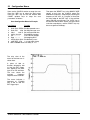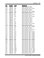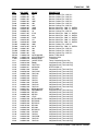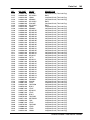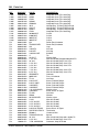
1
MODEL SR620 Universal Time Interval Counter 1290-D Reamwood Avenue Sunnyvale, California 94089 Phone: (408) 744-9040 • Fax: (408) 744-9049 email: [email protected] • www.thinkSRS.com Copyright © 1989 by SRS, Inc. All Rights Reserved. Revision 2.7 (2/2006) SR620 Universal Time Interval Counter Table of Contents i Table of Contents Condensed Information Safety and Use SRS Symbols Specifications Abridged Command List v vi vii xi Operation Width Arming WIDTH:+TIME WIDTH:+TIME, EXT WIDTH:+TIME, EXT with HLDF 13 13 13 13 Rise and Fall Time Arming RISE/FALL: +TIME RISE/FALL: EXT 13 13 13 Quick Start Instructions Instrument Overview 1 2 Frequency Arming Frequency Ratio 14 14 Front Panel Operation 3 Period Arming Period Ratio 14 14 Phase Arming 14 Count Arming Count Ratio 15 15 Delayed Arming Modes 15 Choosing the Measurement Setting the Mode Setting the Source Setting the Arming Mode Setting the Number of Samples Starting Measurements Arming Mode Summary 3 3 3 3 3 3 4 Choosing the Output Display Setting the Front Panel Display Graphics Outputs Graph Types Scaling Graphs Graphics Cursor Graphics Zoom Hardcopy Output Chart Outputs 5 5 6 6 6 6 6 7 7 Setting the Inputs Setting Trigger Levels Setting Trigger Slopes Input Termination UHF Prescalers Input Coupling Reference Output Timebase Input and Output DVM Inputs 9 9 9 9 9 10 10 10 10 Sample Arming 11 TIME Mode 11 Time Interval Arming +TIME +TIME, EXT +TIME, EXT with HOLDOFF +/-TIME +/-TIME, EXT 11 11 12 12 12 12 Configuration Menus 17 CONTROL Menu GPIB Parameters RS232 Parameters 17 17 17 CALIBRATION Menu AutoCal Clock Source 17 18 18 OUTPUT Menu Graphics Enable Printer/Plotter Control Jitter Type Selection Gate Scale Multiplier Trigger Knob Range 18 18 18 19 19 19 SCAN Menu Enabling Scans Setting D/A outputs Scanning the D/A's External Trigger Delays Scan Examples 19 19 20 20 20 20 Specification Guide Definition of Terms Least Significant Digit Resolution Error Differential Non-linearity 23 23 23 23 23 23 SR620 Universal Time Interval Counter ii Table of Contents Timebase Specifications Short-Term Stability Long-Term Stability External Timebases 24 24 24 25 Trigger Input Specifications 25 Measurement Accuracy 26 Programming Programming the SR620 29 Communications GPIB Communication RS-232 Communication Data Window 29 29 29 29 Command Syntax 29 Detailed Command List Trigger Commands Measurement Control Data Transmission Binary Dump Scan Control Graphics Control Front Panel Control Interface Control Status Reporting Calibration Commands Serial Poll Status Byte Event Status Byte TIC Status Byte Error Status Byte 30 30 31 32 33 34 35 36 37 39 39 40 41 41 41 Programming Examples BASIC and RS-232 FORTRAN/National Instruments BASIC/GPIB/Binary Dump FORTRAN/GPIB/Binary Dump C/GPIB/Binary Dump 43 44 45 46 48 52 Scope Display Problems Printer and Plotter Problems GPIB Interface Problems RS-232 Interface Problems Performance Tests 58 58 58 59 61 Necessary Equipment 61 Functional Tests Front Panel Test Self-Test Trigger Input Tests Counter Channel Tests Rear Panel Tests 61 61 61 61 62 62 Performance Tests Timebase Frequency Accuracy Time Interval Trigger Sensitivity Trigger Accuracy D/A Output Accuracy DVM Input Accuracy 63 63 63 63 63 64 64 64 Test Scorecard 67 Calibration 69 Overview 69 Calibration Bytes 69 Simple Calibration 70 Complete Calibration Trigger Input Calibration Clock Oscillator Calibration Insertion Delay Calibration D/A Output Calibration DVM Input Calibration 70 70 71 71 72 73 SR620 Circuitry Test and Calibration Troubleshooting Tips Troubleshooting Power-up Error Messages CAL Error Messages Common Operational Problems Error Messages Error Indicators Wrong Value Excessive Jitter SR620 Universal Time Interval Counter 57 57 57 57 57 57 58 58 58 Circuit Description Processor System GPIB Interface Printer Interface RS-232 Interface Scope Display Counter Input Ports Display Control Ports Front-End Status Bits ADC and DAC Control Bits REF OUT Delay and Gate Generator 75 75 75 75 76 76 76 76 77 77 78 78 Table of Contents Timebase Front-End Inputs Trigger Multiplexers Frequency Gates Event Gating Counting Channels Fast Time Interval Logic Time Interval Arming Time Integrators Analog to Digital Converter Autolevel Circuits Digital to Analog Converter Unregulated Power Supplies Power Supply Regulators Power Supply Bypass Front Panel Display PCB Component Parts List Schematic Circuit Diagrams Front/Rear Panel Summary Counter Visual Index Microprocessor System GPIB/RS232/Printer Interfaces Scope Graphics Controller I/O Ports and LED Drivers Analog and ECL I/O Slow Counters and REF OUT Fast Clocks and Timebase Front-End Input Comparators ECL Mpx/Freq Gating/Counters Fast Time Interval Logic Time Interpolators A/D, D/A and Threshold pots Unregulated Power Supplies Power Supply Regulators Spares and Decoupling Front Panel Display PCB Component Placement on PCB iii 79 79 80 80 81 81 82 82 83 83 83 84 84 84 85 85 87 Sheet No. 1/16 2/16 3/16 4/16 5/16 6/16 7/16 8/16 9/16 10/16 11/16 12/16 13/16 14/16 15/16 16/16 SR620 Universal Time Interval Counter iv Table of Contents SR620 Universal Time Interval Counter Safety and Preparation for Use v Safety and Preparation for Use WARNING: Dangerous voltages, capable of causing death, are present in this instrument. Use extreme caution whenever the instrument covers are removed. This instrument may be damaged if operated with the LINE VOLTAGE SELECTOR set for the wrong ac line voltage or if the wrong fuse is installed. LINE FUSE Verify that the correct line fuse is installed before connecting the line cord. For 100V/120V, use a 1 Amp fuse and for 220V/240V, use a 1/2 Amp fuse. LINE VOLTAGE SELECTION LINE CORD The SR620 operates from a 100V, 120V, 220V, or 240V nominal ac power source having a line frequency of 50 or 60 Hz. Before connecting the power cord to a power source, verify that the LINE VOLTAGE SELECTOR card, located in the rear panel fuse holder, is set so that the correct ac input voltage value is visible. Conversion to other ac input voltages requires a change in the fuse holder voltage card position and fuse value. Disconnect the power cord, open the fuse holder cover door and rotate the fuse-pull lever to remove the fuse. Remove the small printed circuit board and select the operating voltage by orienting the printed circuit board to position the desired voltage to be visible when pushed firmly into its slot. Rotate the fuse-pull lever back into its normal position and insert the correct fuse into the fuse holder. The SR620 has a detachable, three-wire power cord for connection to the power source and to a protective ground. The exposed metal parts of the instrument are connected to the outlet ground to protect against electrical shock. Always use an outlet which has a properly connected protective ground. CONNECTION TO OTHER INSTRUMENTS All front panel BNC shields are connected to the chassis ground and to the power outlet ground via the power cord. Do not apply any voltage to either the shields or to the outputs. The outputs are not protected against connection to any potential other than ground. SR620 Universal Time Interval Counter vi Safety and Preparation for Use SR620 Universal Time Interval Counter Specifications vii Specifications Functions Time Interval, Pulse Width, Rise and Fall Times, Frequency, Period, Phase, and Event Counting. Measurement statistics (mean, min, max, standard deviation or Allan variance) and graphics are available in all modes of operation. Time Interval Time, Width, Rise and Fall Times Range Trigger Rate Least Significant Digit Resolution Error Arming Modes -1000 to +1000 s in +/- TIME mode; -1 ns to +1000 s in all other modes 0 to 100 MHz 4 ps single sample, 1 ps with averaging (((25 ps typ [50 ps max] )2+ (0.2 ppb x Interval)2) / N)1/2 rms (((25 ps typ [50 ps max])2 + (0.05 ppb x Interval)2) / N)1/2 rms (Opt 01) < ±(500ps typ [1 ns max] + Timebase Error x Interval +trigger error) < ±(50ps typ[100ps max] + Timebase Error x Interval) (REL) +TIME Stop is armed by Start +TIME EXT Ext arms Start +TIME EXT HOFF Leading EXT edge arms Start, trailing EXT edge arms Stop. ±TIME Armed by Start/Stop pair ±TIME CMPL Armed by Stop/Start pair ±TIME EXT Armed by EXT input edge EXT arming may be internally delayed or scanned with respect to the EXT input in variable steps. The step size may be set in a 1,2,5 sequence from 1 µs to 10 ms. The maximum delay is 50,000 steps. Display Sample Rate 16 digit fixed point with 1 ps LSD For a sample size of N, the total sample time is N x(800 µs + measured time interval) + Calculation time. The calculation time occurs only after N measurements are completed and varies from zero (N=1, no graphics, binary responses) to 5 ms (N=1, no graphics) to 10 ms (display mean or std dev) to 60 ms (display histogram). Frequency Range Error Gates Display 0.001 Hz to 300 MHz via comparator inputs. 40 MHz to 1.3 GHz via internal UHF prescalers. RATIO A/B range: 10-9 to 103 < ± ((100ps typ [350 ps max])/Gate + Timebase Error ) x Frequency External, 1 period, 1ms to 500s in 1,2,5 sequence. Gates may be externally triggered with no delay. Gates may be delayed relative to an EXTernal trigger. The delay from trigger may be set from 1 to 50,000 gate widths. 16 digit fixed point with LSD = Freq x 4ps/Gate. 1 µHz max. resolution (1 nHz with x1000 for frequencies ≤ 1 MHz) Period Range Error Gates Display 0 to 1000 seconds. RATIO A/B range: 10-9 to 103 < ±((100 ps typ [350ps max])/Gate + Timebase Error) x Period Same as frequency 16 digit fixed point with LSD = 1 ps (1 fs with x1000 for periods ≤ 1 s) Phase Phase = 360 x (Tb - Ta) / Period A Range Resolution -180 to +180 degrees (0 to 100 MHz frequency) (25ps x frequency x 360 + 0.001) degree SR620 Universal Time Interval Counter viii Specifications Gate Error Events Range Count Rate Gates Display 0.01 seconds (1 period min.) for period measurement and 1 sample for time interval measurement. Period may also be measured using externally triggered internal gates as in frequency mode. < ±(1ns x Frequency x 360 + 0.001) degree 1012. RATIO A/B range: 10-9 to 103 0 to 300 MHz Same as frequency 12 digits Timebase Frequency Type Aging Allan Variance (1s)(typ.) Stability 0-50° C Settability External Inputs Threshold Accuracy Sensitivity Autolevel (A&B) Slope Impedance Coupling Input Noise Bandwidth Prescaler (A&B) Protection REF Output Frequency Rise/Fall Amplitude DVM Inputs Full Scale Type Impedance Accuracy Speed D/A Outputs Full Scale Resolution Impedance Standard Option/01 10.000 MHz 10.000 MHz TCVCXO Ovenized VCXO 5x10⁻¹⁰/day 1x10⁻⁶/yr -10 5x10-12 3x10 1 ppm 0.002 ppm 0.01 ppm 0.001 ppm User may supply 5 or 10 MHz timebase. 1 Volt nominal. A, B, and EXTernal -5.00 to +5.00 VDC with 10 mV resolution 15mV + 0.5% of setting see graph next page Threshold set between peak input excursions. (f>10 Hz, duty cycle >10-6) Rising or falling edge (1 M Ohm + 30 pf) or 50 Ohms. 50 Ohm termination has SWR < 2.5:1 from 0 -1.3GHz AC or DC. Ext is always DC coupled. 350mV rms typical 300 MHz BW provides 1.2 ns risetime see graph next page 100 V. 50 Ohm terminator is released if input exceeds ±5 Vpeak. Calibration and Trigger source 1.00 KHz (Accuracy same as timebase) 2 ns TTL: 0 to 4 VDC (2 VDC into 50 Ohms) ECL: -1.8 to -0.8 VDC into 50 Ohms Two differential rear panel DVM inputs ±1.999 or ±19.99 VDC Sample & hold with successive approximation converter 1 M Ohm 0.3% of full scale Formatted response in approximately 5 ms. Two rear panel outputs which may be ramped ±10.00 VDC 5 mV < 1 Ohm SR620 Universal Time Interval Counter Specifications Default Accuracy Graphics Scope Displays X-axis Y-axis Resolution Hardcopy ix Voltage proportional to Mean & Deviation 0.3% of full scale Live scope displays and hardcopy Two rear panel outputs to drive x-y scope Histograms and strip charts of mean & deviation -5 to +5 V for 10 division deflection -4 to +4 V for 8 division deflection 250 (H) x 200 (V) pixels Via Centronics port to Epson graphics compatible dot matrix printers. RS-232, IEEE-488 to HP-GL compatible Digital Plotters. Interfaces RS-232C GPIB Speed 300 to 19.2 KBaud. All instrument functions may be controlled. PC compatible serial cable. IEEE-488 compatible interface. All instrument functions may be controlled. Approximately 150 ASCII formatted responses per second. 1400 binary responses per second. General Operating Power Dimensions Weight 0 to 50° C 100, 120, 220 or 240 VAC +5% -10%. 50/60 Hz. 70 Watts. 14" x 14" x 3.5". Rack mounting hardware included. 11 lbs SR620 Universal Time Interval Counter x Specifications SR620 Universal Time Interval Counter Abridged Command List xi Abridged Command List Syntax Variable i is an integer that selects an input channel for the command: i 0 1 2 Channel External Gate A input B input Variables i,j,k,l,m, and n are all integers.Variable x is a real number in integer,real, or exponential notation. Commands which may be queried have a ? in parentheses (?) after the mnemonic. The ( ) are not sent. Commands that may only be queried have a '?' after the mnemonic. Commands which may not be queried have no '?'. Optional parameters are enclosed by {}. Trigger Control Commands LEVL(?) i,x MTRG j RLVL(?) j TCPL(?) i{,j} TERM(?) i{,j} TMOD(?) i{,j} TSLP(?) i{,j} Set channel i threshold to x volts. Only allowed in remote operation. Same as pushing MAN trigger button. In external gate or holdoff arming modes n=0= start gate, n=1= stop gate. Otherwise n is ignored. Sets the reference output level to 0 = ecl,1=ttl. Sets the input ac/dc coupling of chans A and B to 0 = dc, or 1 = ac. Sets the 50 ohm terminator of input, also prescaler n=0= 50 ohm, n=1= 1 meg, n= 2 = prescale. Prescalers can only be used in freq and per modes. Sets autolevel on/off. 0 = auto off, 1 = auto on. Set the trigger slope to 0 = positive, 1 = negative. Measurement Control Commands *TRG ARMM(?) j Device trigger, same as pushing start button Sets the arming mode 0 +- time 1 + time 2 1 period 3 0.01 s gate 4 0.1 s gate 5 1.0 s gate 6 ext trig +- time 7 ext trig + time 8 ext gate/trig holdoff 9 ext 1period 10 ext 0.01 s gate 11 ext 0.1 s gate 12 ext 1.0s gate AUTM(?) j COMP DREL(?) j Sets/resets autostart of measurements. 0 = off,1= on Complements parity in +-time arming Sets/clears the display REL. 0 = clear, 1 = set, 2 = clear REL and display, 3= set rel to position of cursor. Sets the value of the frequency, period, of count gate to x. x may bebetween 1ms and 500s in a 1,2,5 sequence. If x < 0 a externally triggered gate of length x is set. Sets variance type to 0 = std dev, 1= Allan variance. GATE(?) x JTTR(?) j SR620 Universal Time Interval Counter xii Abridged Command List MODE(?) j SIZE(?) j SRCE(?) j STRT STOP Sets the instrument mode to 0 = time,1 = width, 2=tr/tf, 3 = freq, 4 = period, 5 = phase, 6 = count. Sets the number of samples. Sets the measurement source to 0 = A, 1= B, 2= REF, 3 = ratio. Same as pushing start button. Same as pushing stop button. Data Commands MEAS? j XALL? XAVG? XJIT? XMAX? XMIN? XREL(?) x XHST? j HSPT? j SCAV? j SCJT? j BDMP j Startts a measurement and returns the result when it is complete. If j=0 the mean is returned, j=1 returns the jitter, j=2 returns the max, and j=3 the min. Returns mean,rel,jitter,max,min of a measurement. Returns the mean of measurement. Returns the jitter of a measurement. Returns the max of a measurement. Returns the min of a measurement. Sets the value of the display rel to x. Returns section j of the histogram display as 4 byte binary integers.j=0 to 9. Return the value of the point n on the histogram. j=1 to j = 250. Returns 9E20 if graph is blank. Returns the value of point n (1 - 250) of the mean stripchart or the value of scan point j. returns 9E20 if the stripchart is blank or the scan has not reachedpoint j. Returns the value of point n (1 - 250) of the jitter stripchart or the value of scan point j. returns 9E20 if the stripchart is blank or the scan has not reached point j. Binary dumps j points. Sample size = 1. Scan Commands ANMD(?) j DBEG(?) j DSEN(?) j DSTP(?) x HOLD(?) x SCAN SCEN(?) j SCLR SLOC? SCPT(?) j VBEG(?) j,x VOUT? j VSTP(?) j,x Sets the DAC output mode of the mean and jitter DAC's to 0 = chart/chart, 1= DAC/chart, 2= chart/DAC,3 = DAC/DAC. Sets the delay scan start position to 1-50000 step sizes after the external trigger Enables the internal delay scan . 0 = delay off, 1=delay hold, 2 = delay scan. Sets the delay scan step size to 1,2,5 x 10 -2,-3,-4,-5,-6. 1 x 10 –2 is the maximum step size. Sets the hold time between scan points from .01s to 1000 s in .01 s steps Clears and restarts a scan. Enables scanning. 0 = disabled,1= single scan mode 2 = repeat scan mode Clears the scan. Returns the number of the last completed scan point. Returns 0 if no points are complete. Sets number of scan points to 2,5,10,25,50,125,250. Sets the DAC output scan starting voltage. If scans are disabled or the step size is zero the output is immediately set to the new voltage. Otherwise, the voltage is updated at the start of the next scan. Reads the current output voltage of DAC channel j. Sets the DAC scan step size to x volts. Graphics Control Commands AUTP(?) j AUTS CURS (?) j DGPH(?) j GCLR Sets the autoprint mode to 0 = off or 1 = on. Autoscales the displayed graph. Sets the cursor position to j. Sets the displayed graph to 0 = histogram,1= mean,2 = jitter Clears the displayed graph. SR620 Universal Time Interval Counter Abridged Command List GENA(?) j GSCL(?) j,x PDEV(?) j PLAD(?) j PLPT(?) j PLOT PCLR xiii Turns graphs 0 = off, 1 = on. Sets the graph scales. j = 0 = histogram verticalscale,j=1= histo horizontal,j=2=histo bins,j=3= mean graph scale,j = 4= jitter graph scale. x = units per division or # bins. Sets output device to 0 = printer, 1= plotter. Sets the plotter GPIB address. Sets the plotter port to 0= RS232 , 1= GPIB. Initiates a print/plot Clears plots/prints Front Panel Control DISP(?) j EXPD(?) j KEYS(?) j Sets the display source. 0=MEAN,1=REL,2=JITTER,3=MAX 4 =MIN, 5 = TRIG, 6 = DVM's Set the x1000 expand status in freq and per mode 0 = off, 1 = on Simulates a keypress, or reads the most recently pressed key Rear Panel Control CLCK(?) j CLKF(?) j PORT(?) j PRTM(?) j RNGE(?) i{,j} VOLT? j Sets the clock source. 0 = internal, 1= external. Sets the external clock frequency. 0=10MHz,1= 5MHz. Sets/reads the binary I/O port when enabled. Sets the printer port mode. 0 = print, 1 = input,2 =output. Sets the full scale voltage of DVM input i. Reads DVM channel 0 or 1. Interface Control Commands *RST *IDN? *OPC(?) *WAI ENDT {j,k,l,m} LOCL j WAIT(?) j Clears instrument to default settings. Returns the device identification . Operation complete common synchronization command. Either sets a status bit or returns a value when all operations (scans , prints, measurements) are complete. Wait synchronization command. Holds off further command execution until all in progress operations (scans, prints,measurements) are complete. Sets the RS232 end transmission terminator Sets the RS232 local/remote function. 0 = local, 1=remote, 2 = local lockout Sets the RS232 intercharacter time delay. Status Reporting Commands *CLS *ESE(?) j *ESR? {j} *PSC(?) j *SRE(?) j *STB? {j} EREN(?) j ERRS? {j} STAT? {j} TENA(?) j STUP? Clears all status registers. Sets/reads the standard status byte enable register. Reads the standard status register, or just bit j of register. Sets the power on status clear bit. This allows SRQ'son power up if desired. Sets/reads the serial poll enable register. Reads the serial poll register, or just bit n of register. Sets/reads the error status enable register. Reads the error status register, or just bit n of register. Reads the TIC status register, or just bit n of register. Sets/reads the TIC status enable register. Returns the complete setup in one string. Calibration Control (NOTE: these commands are not needed during normal operation) $TAC? j $PHK? j Reads the value of the time-to-amplitude converters. Sets the printer handshake lines. SR620 Universal Time Interval Counter xiv Abridged Command List $POT? j *CAL? *TST? BYTE(?) j,k WORD(?) j,k Reads the value of trigger pot j Starts autocal and returns status when done. Starts self-test and returns status when done. Reads/sets linearization byte values. Reads/sets cal words. SR620 Universal Time Interval Counter Quick Start Instructions 1 Quick Start Use this procedure as a quick orientation to the instrument's features and capabilities. If you encounter problems, read the detailed discussions on operation or see the troubleshooting section. MEAN. The REL LED will turn on and the display will show a mean value within a few ps of zero. An 'r' appears on the display to indicate a relative value. 6) Press the DISPLAY down-key to show each of the following: 1) Make sure that the correct line voltage has been selected on the rear panel power entry module. 2) With the unit's power switch on "STBY", hold the "CLR" key in the "DISPLAY" section down and turn the unit "ON". This will return all of the instrument settings to their default state. The message, "SELF TEST PASS" should briefly appear. Note: The fan will not run until the unit warms up. The red LED labeled "CLOCK" in the CONFIG section may stay on for a few minutes. The red LED's labeled "START" and "STOP" may blink if no inputs are applied. 3) Press the MODE down key once to select the WIDTH mode. Press the source key twice to select REF ( the 1 kHz REFerence ) as the signal source. After 1/2 hour warmup, the display should read 500 us +- 1 ns. If the displayed value is outside this range see instructions for running the AUTOCAL procedure. 4) Press the SAMPLE SIZE up-key five times to select a sample size of 500. This will slow the display update rate to 2 Hz, and provide a more consistent MEAN value. 5) Press the SET key in the DISPLAY section to set the REL offset to the current value of the MEAN REL JITTER MAX MIN TRIG DVM 0+-100 ps (The REL is set) 500 us +-100 ps 5-20 ps Erratic, but usually <100 ps Erratic, but usually <100 ps +-5 V per the three level knobs Within 5 mV of zero. 7) Configure an oscilloscope for the X-Y display mode with the horizontal and vertical inputs set for dc coupling ( not 50 Ohms ) and 1 V/div sensitivity. If the scope has scale factor displays, turn them "off", and set the 20 MHz bandwidth limit. Center the beam in the middle of the screen and attach the inputs to the X-Y display outputs on the rear panel of the SR620. 8) Press the AUTO key in the SCOPE AND CHART section to scale the display. If the DISPLAY REL is set, the HISTOgram of the pulse widths will be displayed with about 20 ps/div horizontal resolution. 9) In the SCOPE AND CHART section, press the display button to change from HIST to MEAN. Press the AUTO button to scale the display. The scope will now show a 'strip chart' of the mean values for each set of measurements. Now select JITTER and press AUTO to display a 'strip-chart' of standard deviations for the scope display. SR620 Universal Time Interval Counter 2 Instrument Overview The SR620 Time Interval Counter can do a variety of time interval and frequency measurements. The instrument's high single-shot timing resolution, low jitter, and reciprocal counting architecture allow rapid, high resolution measurements. Frequency gating modes include fixed gates of one period, 0.01 s, 0.1 s, 1 s, Externally triggered fixed gates, External gates, Externally triggered adjustable gates from 1 us to 10 ms. Gates which are externally triggered may be delayed and scanned by 1 to 50,000 gate widths to allow transient frequency measurements. Modes of Operation Statistics Time Intervals between the A and B inputs may be measured with 4 ps LSD, 25 ps rms resolution, 100 ps relative accuracy, and 1ns absolute accuracy. Time intervals from -1ns to 1000 s or +1000 s may be measured. The SR620 will compute and display statistics for sample sizes of one to one million . The mean, standard deviation or Allan variance, minimum and maximum deviations may be displayed. Statistics are available for all modes of operation. Displayed values may be offset by the REL for measurements relative to a previous mean value. Introduction Pulse Widths of either input may be measured. The start and stop thresholds are set separately. The resolution, jitter, and accuracy are the same as for Time interval measurements. Rise and Fall Times of either input may be measured. The start and stop thresholds may be set with 10 mV resolution. The 350 MHz bandwidth of the inputs allows measurements of rise and fall times down to 1 ns. Frequencies from 0.001 Hz to 1.3 GHz may be measured. The SR620 will provide 11 digits of resolution when a one second gate is used. Frequencies above 300 MHz may be measured on either input using the UHF prescalers. NanoHertz resolution is available in the x1000 display mode. Periods may be measured with femtosecond resolution. Period measurements are done the same way as frequency measurements, except the reciprocal of frequency is reported to the display. The Phase between the signals on the A and B input may be measured with 0.001° resolution. The phase shift between signals from 0.001 Hz to 100MHz may be measured. The Count mode is used to count input transistions during a gate. Count rates up to 300 MHz will be tallied. Arming and Gating Each of these modes are supported with powerful arming and gating modes. Time arming modes include: +Time, +Time External, +Time External with Stop Holdoff, +-Time, and +-Time External. SR620 Universal Time Interval Counter Scope Displays and Hardcopy The SR620 can display histograms and strip charts on any xy scope. Histograms show the distribution of values within a group of measurements. Strip charts of the previous 250 mean values or deviations show data trends. Hardcopy of scope displays may be made to printers or plotters via rear panel Centronics, RS232 or GPIB ports. Reference Output The front panel REF OUT provides a precision 1KHZ square wave at TTL or ECL levels. This source may be used for calibration, and is a convienent trigger for many types of measurements. DVM's and DAC Outputs Two rear panel DVM inputs allow dc voltage measurements with 0.3% accuracy on 2 or 20 V full scale ranges. The inputs may be displayed on the front panel or read via the RS232 or GPIB interfaces. Two DAC outputs default to output voltages proportional to the mean and jitter readings to drive analog strip chart recorders. The DAC output voltages may also be set or scanned from the front panel of through one of the computer interfaces. Computer Interfaces Both GPIB and RS232 interfaces allow complete control of the instrument. A fast binary dump mode allows up to 1500 measurements per second to be taken and transfered to a computer. Front Panel Operation 3 FRONT PANEL OPERATION The SR620 Universal Time Interval Counter can perform an extremely wide variety of time interval and frequency measurements. The SR620 is designed so that the values of virtually all of the important measurement parameters are visible at a glance on the front panel. Setting the SR620 to perform a particular measurement can be separated into three steps: choosing the measurement, choosing the output display, and setting the inputs. The SR620 is different than most counters in that a "measurement" consists of from 1 to 1,000,000 "samples" and the SR620 reports statistical information on these samples. The SR620 can report the mean , jitter, maximum , and minimum values found in a measurement. CHOOSING THE MEASUREMENT SETTING THE MODE Pressing the MODE up and down arrow keys sets the measurement type. The SR620 can measure time intervals, pulse widths, pulse rise and fall times, frequency, period, phase, and can count events. The ARMING section has detailed explanations of the modes. SETTING THE SOURCE The source key selects the signal source for a particular measurement. In time interval mode the source specifies which input will "start" the time interval. Normally the start source is channel A, but channel B, and the 1kHz REF output may also be selected. The other input then "stops" the time interval. In pulse width, frequency, period, and counts the source may be A, B, or the 1kHz REF. Additionally, in frequency, period, and count modes if both the A and B LEDs are on the RATIO A/B is measured. In rise/fall time mode only A and B may be the source, while in phase mode the phase of B relative to A is always measured. SETTING THE ARMING MODE modes. The various modes relevant to each particular type of measurement are treated in detail in the ARMING section of this manual. A summary of the arming modes is given on the next page. SELECTING THE NUMBER OF SAMPLES The sample size up and down arrow keys select between 1 and 1,000,000 samples for the measurement. STARTING AND STOPPING MEASUREMENTS The "START" and "RESET" keys start and stop measurements. Press the "START" key to start a single measurement. The "BUSY" LED will remain on while the measurement is in progress. When the measurement is finished the SR620 will display the results and stop. Press and hold the START key to turn on the "AUTO" LED and "automeasure". When automeasure is on the SR620 will automatically start a new measurement when the present one is complete. Press the "RESET" key to terminate the present measurement. Press and hold the "RESET" key to turn the "AUTO" LED and automeasure off. "Arming" controls the conditions under which a sample is started and stopped. The arming mode is chosen using the ARMING up and down arrow keys. The SR620 has a large selection of arming SR620 Universal Time Interval Counter 4 Front Panel Operation SUMMARY OF ARMING MODES mode arming mode LED indication time +TIME +TIME EXTERNAL +TIME EXTERNAL STOP HOLDOFF +TIME LED on +TIME and EXT LEDs on * +TIME, EXT, and HLDF LEDs on * ±TIME ±TIME COMPLEMENT ±TIME EXTERNAL ± TIME LED on ±TIME and CMPL LEDs on ±TIME and EXT LED on * width,rise/fall time +TIME +TIME EXTERNAL +TIME EXTERNAL STOP HOLDOFF +TIME LED on +TIME and EXT LED on * + TIME, EXT, and HLDF LEDs on * frequency,period 1 PERIOD 0.01s gate 0.1s gate 1.0s gate ext gate ext 1 PERIOD ext 0.01s gate ext 0.1s gate ext 1.0s gate 1 PERIOD LED on 0.01s LED on ** 0.1s LED on ** 1.0s LED on ** EXT LED on * EXT and 1 PERIOD LEDs on EXT and 0.01s LEDs on ** EXT and 0.1s LEDs on ** EXT and 1.0s LEDs on ** phase +TIME EXT +TIME LED on EXT LED on * count 0.01s gate 0.1s gate 1.0s gate ext gate ext 0.01s gate ext 0.1s gate ext 1.0s gate 0.01s LED on ** 0.1s LED on ** 1.0s LED on ** EXT LED on * EXT and 0.01s LEDs on ** EXT and 0.1s LEDs on ** EXT and 1.0s LEDs on ** NOTES: * arming delay or scanning delay/gate may be used in this mode (see CONFIGURATION MENU and ARMING sections). The EXT LED will flash if scanning is enabled. ** the gate time LED will flash if gate width multiplier is not equal to 1 (see CONFIGURATION MENU and ARMING sections). SR620 Universal Time Interval Counter Front Panel Operation 5 CHOOSING THE OUTPUT DISPLAY The SR620 can display statistical information about the measurement of N samples. The SR620 computes and reports the mean, standard deviation or root Allan variance, minimum, and maximum values seen during the measurement. The equation for the statistical functions are given by: pressing the "CLR" button. Normally the REL is set to the value of the mean when the "SET" button is pressed. However, the REL may be set to an arbitrary value using the ZOOM feature described in the GRAPHICS ZOOM section below. Pressing the "CLR" button with the REL off clears the display. JITTER: displays either the standard deviation (display prefaced by "d") or Allan variance ( display prefaced by "A"). The statistic that is used is set in the CONFIGURATION MENU. MAX: displays the maximum sample found in this measurement. If the display is prefaced by "r" then a relative reading is displayed and the value displayed is the max minus the REL. MIN: displays the minimum sample found in this measurement. If the display is prefaced by "r" then a relative reading is displayed and the value displayed is the min minus the REL. SETTING THE FRONT PANEL DISPLAY The DISPLAY up and down arrow keys control what is displayed on the 16 digit LED display. All of the statistical data is always calculated and may be viewed by scrolling through the displays. The settings are: MEAN: displays the mean value of the measurement. If the display is prefaced by "r" then a relative reading is displayed and the value displayed is the mean minus the REL. REL: displays the value of the REL. The REL is set by pressing the "SET" button and is cleared by TRIG: displays the trigger level set by the EXT, A, and B trigger knobs (The full scale range of the knobs may be set in the CONFIGURATION MENU.). DVM: displays the voltage values at the rear panel DVM inputs. Pressing both the up and down arrow keys together toggles the x1000 expand on and off in frequency and period mode. In frequency mode the x1000 expand moves the decimal point 3 places to the left and displays frequencies with nHz resolution. The maximum frequency measurable in this mode is 1 MHz. In period mode the x1000 expand moves the decimal point 3 places to the left and displays periods with fs SR620 Universal Time Interval Counter 6 Front Panel Operation resolution. The maximum period measurable in this mode is 1 s. In both period and frequency modes the statistical data is displayed with the number of significant digits allowed by the SR620's resolution. Using longer gate times increases the resolution. GRAPHICS OUTPUTS In addition to the 16 digit LED display the SR620's scope and chart outputs may be used to give the user alternative methods of viewing the data. SCOPE OUTPUTS The SR620 may be attached to an oscilloscope operating in x-y mode to provide a graphical presentation of the output data. The oscilloscope should be set in x-y mode with sensitivities set to 1V/div and the SR620's x and y rear panel outputs attached. that the data fits on the screen. In histogram mode the actual scaling of the graph does not occur until the next measurement is complete. The scale may also be adjusted manually. Pressing the up and down arrow keys with the normal display on the 16 digit LEDs will adjust the vertical scale on the displayed graph. In the histogram mode , incrementing the vertical scale past the largest value (200,000 / div) will change the vertical scale to a log scale. To view the scales on the LED display press the "DISP" button. First, the cursor position (discussed below) will be displayed. Pressing the button again will display the vertical graph scales in the appropriate units. In the histogram mode pressing the button again will display the horizontal scale and then the number of bins. The scales may be adjusted using the up and down arrow keys. When the REL is set the graphs are centered about the REL and, thus, very fine detail may be observed on a large number. GRAPHICS CURSOR GRAPH TYPES The SR620 can then display either a histogram of number of samples vs. measured parameter for the samples within a measurement, a stripchart of mean values for successive measurements, or a stripchart of jitter values for successive measurements. In histogram mode a new graph will be displayed after each measurement of N samples is complete, showing the distribution of samples in that measurement. In the stripchart modes a new point will be added to the graph after each measurement indicating the mean and jitter values for that measurement. The display desired is chosen by pressing the select button below the indicator LEDs. The data for all three graphs are saved so that all of the graphs may be viewed by cycling through the three choices. The data, the scale values, and the cursor position are all displayed on the scope screen. In the stripchart modes up to 250 points will be displayed. When the display fills up new data will start to overwrite the old starting from the left. The graph may be cleared by pressing the CLR button below the PRINT button. SCALING GRAPHS In histogram mode the vertical scale, horizontal scale, and number of bins may be adjusted. In the stripchart modes the vertical scales may be adjusted. The easiest way to scale the graphs is to press the "AUTO" button to autoscale the graph. Autoscale will automatically adjust the scales so SR620 Universal Time Interval Counter The displayed graphs have a moveable cursor that allows one to read the values of individual points on the screen. The cursor is represented on screen by a dotted line. The cursor is moved by pressing the "DISP" button to display the cursor position and using the up and down arrow keys to move it about. The cursor x position is displayed on the LED display ( in the correct units of s, Hz, etc.) for the histogram display and measurement number for the stripcharts. Both the x and y positions are displayed on the scope screen. GRAPHICS ZOOM The SR620 has a feature which allows one to zoom in on any feature in a displayed histogram, this feature also allows the REL to be set to any value desired. First, press the DISP button to display the cursor position. Then, move the cursor until it is at the desired position ( or the cursor value is the desired REL value if setting the REL). Push the "SET" button. This will set the REL to the cursor position. Now, adjust the graph horizontal scale to get the magnification desired. If setting the REL value, note that the amount that the cursor value changes for each press of the arrow keys is determined by the horizontal histogram scale and that the scale may have to be adjusted to get the REL value desired. Front Panel Operation HARDCOPY OUTPUT The displayed graph may be copied to either an Epson compatible graphics printer or a HP-GL compatible plotter by pressing the "PRINT" key. The SR620 will continue to take data while the hardcopy is being generated. If a second print/plot request is made (by pressing the button or a programming command) before the current copy is finished the SR620 will stop taking data until the current copy is done. This is to avoid corrupting the second copy as the SR620 only has a 1 deep graphics output queue.The output device (printer or plotter) is chosen in the CONFIGURATION menu (see that section for detail). When using a printer the SR620 may be put into autoprint mode by pressing and holding the PRINT key until the "AUTO" LED turns on. In autoprint mode the SR620 will automatically print every histogram or a new stripchart each time the stripchart fills up. There is no autoprint when using a plotter because the paper needs to be changed. In autoprint mode the speed of the printer may determine the measurement rate if new graphs are generated 7 faster than the printer can print them. A print or plot may be aborted by pressing the "CLR" button under the PRINT button. Pressing and holding the CLR button will turn off autoprint. If the message "print error" or "plot error" appears while printing or plotting please refer to the TROUBLESHOOTING section. CHART OUTPUTS In addition to the scope outputs the SR620 also has two rear panel analog outputs designed to go to analog chart recorders. One output puts out a voltage proportional to the mean of the measurement while the other output puts out a voltage proportional the jitter of the measurement. The output range is 0-8V corresponding to the 8 vertical scope divisions. The scale is the same as the scope scales. In the cases where zero is at the center of the scope screen (the REL is set, for example) zero will correspond to 4 volts output. The chart outputs may also be configured as general purpose D/A outputs (see CONFIGURATION MENU section). Sample Histogram. The graph scales are 20ps/div in the horizontal direction and 10 /div in the vertical. The REL is 500.000023 us and is at the center of the graph. This measurement has a mean value 6ps greater than the REL and a standard deviation of 9ps. The cursor (dotted line) is at the REL and there are 46 events in that bin. SR620 Universal Time Interval Counter 8 Front Panel Operation Sample mean value graph. Each point corresponds to the mean value from one measurement. The vertical scale is 10 Hz/div. The measurements are relative to a REL of 10.022176 kHz. The REL is at the center of the graph. The cursor (dotted line) shows that measurement number 67 was 1.635 kHz below the REL. Sample jitter stripchart. This graph shows the jitter associated with each measurement above. The vertical scale is 10 Hz/div. The cursor is at measurement number 165 and the jitter value there is 32.6 Hz. SR620 Universal Time Interval Counter Front Panel Operation 9 SETTING THE INPUTS SETTING TRIGGER LEVELS SETTING TRIGGER SLOPES The trigger levels are set by rotating the trigger level adjust knobs. These knobs may have a full scale range of ±5.00V, ±2.50V, or ±1.25V. The full scale range is set in the CONFIGURATION menu (see that section of the manual for details). In all cases the trigger level resolution is 10mV and the actual level may be displayed on the front panel. The trigger inputs have about 40mV of hysteresis and the trigger levels are corrected for this hysteresis so that the inputs will trigger at the selected voltage independent of the selected trigger slope. The A and B inputs can be set to trigger on either a rising or falling edge by pressing the "SLOPE" buttons. The EXT input can be set to rising edge or falling edge by pressing the "LOGIC" button. If the EXT input is being used to supply a gate pulse the SR620 will use the time above threshold as the gate if POSitive logic is selected and the time below threshold as the gate if NEGative logic is selected. The LED's above the trigger knobs will flash when the input comparator triggers. The A and B inputs may also be set to autolevel by rotating the knobs completely counter-clockwise. The "AUTO" LED under the knob will come on and the trigger threshold will automatically be set to the midpoint of the signal. Autolevel will work for a signal faster than about 10Hz and a duty cycle greater than about 0.0001%. The autolevel circuit will not change the trigger level until the input stops triggering for more than 1/2 second. Then it will try to reset the trigger level to a new value. The red LEDs behind the words "START" and "STOP" will flash each time the autolevel circuit tries to adjust the trigger threshold. NOTE: in width and rise/fall time modes, which use only one input, the A trigger knob sets the start trigger voltage and the B trigger knob sets the stop trigger voltage. INPUT TERMINATION The EXT, A, and B input may all be terminated in either 1MOhm or 50 Ohms by pressing the "INPUT" or "TERM" buttons. If the inputs are terminated in 50 ohms and the input signal exceeds ±6V peak the 50 Ohm terminator will automatically be removed to prevent damage to the terminator. When this overload condition occurs the 50 ohm LED will flash. UHF PRESCALERS In frequency and period modes the input signal may be fed to the SR620's UHF prescalers to measure signals between 40MHz and 1.3GHz. To engage the prescalers press the "INPUT" button for the desired channel repeatedly until the UHF LED comes on. The sensitivity of the prescalers may be adjusted by adjusting the channel A and B trigger knobs. Setting the knobs for 0V or to autolevel will set the sensitivity to maximum. Setting the knobs to 5V will reduce the sensitivity SR620 Universal Time Interval Counter 10 Front Panel Operation to about 200mV rms. Both positive and negative settings of the knob have the same effect. The sensitivity adjustment is useful because at maximum sensitivity the prescalers will selfoscillate with no signal input. With an input, however, this is not a problem, but by reducing the sensitivity slightly these oscillations will disappear. INPUT COUPLING The A and B inputs may be either AC or DC coupled by pressing the AC/DC button. The coupling is independent of the input termination impedance. The EXT input is always DC coupled. REFERENCE OUTPUT The front panel REF output puts out a 1kHz 50% duty cycle square wave synchronized to the SR620's internal 10MHz clock. This output may provide 4V into high impedance or 2V into 50 Ohms, or ECL levels into 50 Ohms. An example of the use of this output is to set the mode to measure the time from REF to B. If a cable is then connected from the REF output to B the cable delay may be directly measured. SR620 Universal Time Interval Counter TIMEBASE INPUT AND OUTPUT A rear panel BNC outputs the SR620's 10MHz clock. This output supplies approximately 1V pkpk into a 50 ohm load. Another BNC allows the input of a 5 or 10 MHz external timebase. This input presents a 1 kOhm load to the signal. The SR620 can then phase-lock its internal timebase to this external source. See the CONFIGURATION MENU chapter for detail on using an external timebase. DVM INPUTS The SR620 has two rear panel DVM inputs. These 1 MOhm differential inputs allow the SR620 to measure DC voltages on either a 2V or 20V full scale range. The SR620 can either autorange the inputs (default) or they may be set to a fixed scale. See the CONFIGURATION MENU chapter for detail on setting the DVM scales. Sample Arming 11 SAMPLE ARMING The SR620 Time Interval counter has a wide variety of arming modes that allow the user great flexibility in controlling the desired measurement. The various measurement modes and their respective arming modes are discussed in detail below. When REF is used as the Start source, the rising edge of REF is used when a positive slope is selected for the A input, and the falling edge is used when a negative slope is set. In this case, the threshold knob above the A input has no effect on operation. NOTE: references to delayed or scanning gates are discussed at the end of this section TIME INTERVAL ARMING TIME MODE In this mode, the unit measures the time interval between a Start and a Stop pulse. The time interval is a positive number if the Start occurs before the Stop and negative if the Stop occurs before the Start. The SOURCE LED's indicate the source of the START pulse. There are several arming modes for Time interval measurements. The arming mode controls when the instrument will be ready to take a sample. Start and Stop pulses are ignored when the instrument is not armed. The ARM LED will turn on when the unit is armed. The SR620 remains busy for about 800us after receiving a Start/Stop pair and may not be rearmed during this time. +TIME MEASUREMENTS (-1ns to 1000s) Source LED A B REF Start Source A B REF Stop Source B A B In +TIME arming the Start input is armed as soon as the instrument is ready and Stop is armed when a Start is received. In this mode only a positive or zero time interval may be measured. (The knobs which are directly above each input set the voltage threshold for that input when in the TIME mode.) Usually, A will be selected as the Start source and the time interval from A to B will be measured. The internal 1kHz REF output may be selected in cases where the front panel REF out will be used to trigger an event, and the "event" will provide a Stop pulse to the B input. A simple example of this would be the measurement of cable lengths. The length of a cable may be measured by selecting REF as the Start source, and connecting the cable between the REF output and the B input. In +TIME EXTERNAL mode the Start input is enabled by the GATE and Stop is armed by Start. A delay from an EXT input may be set or scanned in the CONFIG menu, otherwise the EXT input will be the trigger. Time Arming Mode Function +TIME +TIME EXTERNAL +TIME EXTERNAL STOP HOLDOFF Start arms automatically, Stop is armed by Start Start is armed by EXT input, Stop armed by Start Start is armed by leading edge of EXT input and the Stop is armed by the trailing edge. ±TIME ±TIME COMPLEMENT ±TIME EXTERNAL Starts and Stops are armed by Start/Stop pair Starts and Stops are armed by Stop/Start pair Starts and Stops are armed by EXT input SR620 Universal Time Interval Counter 12 Sample Arming TIME EXTERNAL with HOLDOFF is similar except that Stops are not enabled until the trailing edge of the EXT input. A particular Stop pulse may be selected to end the time interval by using the EXT input to inhibit, or holdoff, the Stop input. An example of this might be measuring the time from the index mark on a hard disk drive to a particular data bit. By adjusting the holdoff time one could measure the time to any data bit instead of just the first one. The trigger may be delayed or scanned from an EXT trigger input by setting SCAN parameters in the CONFIG menu. A blinking EXT LED indicates that the EXT is used as a trigger for the delayed gate. ±TIME MEASUREMENTS (-1000s<t< 1000s) In all of the ± TIME modes Starts and Stops are armed simultaneously and so either a positive or negative time interval may be measured. There is, unfortunately, some ambiguity to this method of arming. For periodic inputs there is no way for the instrument to know if the desired time interval should be measured from the Start to the previous Stop or to the next Stop. For example, if the Start SR620 Universal Time Interval Counter and Stop are both 1 KHz square waves, with the Stop edge following the Start edge by 1 uS, then the unit will report a Time interval of either +1 us or -999 us. In the ±TIME and ±TIME COMPLEMENT modes the start and stop inputs are armed by parity, that is, the reception of either a Start/Stop pair or a Stop/Start pair of pulses. By changing between these two modes one may choose to measure either the time from Stop to the next Start or Start to the next Stop. Since the parity of the input signals is randomly determined at power-up there is no way to specify which arming mode will correspond to which measurement. But by changing between these modes both measurements may always be obtained. Alternately, one may arm a ±Time measurement with a signal applied to the Ext input in which case the measurement that is made (Start to Stop or Stop to Start) is determined only by the relationship of the Ext input to the Start and Stop signals. The EXT input requires about 10 ns setup prior to the Start or Stop inputs. Time intervals as a function of delay from an EXT trigger may be measured by using the internal delay generator. The delay generator is triggered by the EXT input. The trigger delay may be set or scanned via the CONFIG Menu. Sample Arming Time interval samples may also be armed by pressing the MAN key when in the EXT arming mode. WIDTH Pulse widths may be measured in the WIDTH mode. The pulse source may be either the A input, the B input, or the internal 1 kHz REF source. The Start threshold and slope are set by the controls just above the A input. The Stop threshold and slope are set by the controls just above the B input. If the Start slope is positive, the Stop slope will be negative, and the time from a rising edge to a falling edge will be measured. These controls are not used when measuring the width of the internal 1 KHz REF. As pulse widths are always positive times, only the +TIME arming modes are available. The three arming modes for WIDTH measurements are shown here. The trigger source may be either the EXT input or the EXT triggered internally delayed/scanned gate. 13 RISE and FALL TIMES The transition time for an input may be measured in this mode. Either the A or B input may be selected as the source to be measured. The selected source is used as the input to both comparators. The threshold knob above the A input is used to specify the Start voltage threshold, and the knob above the B input is used to specify the Stop voltage threshold. The rise time of the input is reported if positive slope is selected, and the fall time is reported if negative slope is selected. Either slope key changes both comparators' slope LED's. For example, to measure the 20-80% rise time of a one volt input, the A threshold would be set to 0.20 VDC, the B threshold would be set to 0.80 VDC, and the slope would be set to positive to measure the rising edge. The 80-20% transition time of the falling edge could be measured by setting the slope to negative and adjusting the trigger thresholds. Reported times are not corrected for the finite bandwidth of the input of the instrument. The inputs have a bandwidth of about 300 MHz, and so the 10-90% transition time of an infinitely fast input would be reported as 1.2 ns. When measuring 10-90% transition times, the actual transition time may be found by: T actual = sqrt (T measured2 - 1.2 ns2 ) As transition times are always positive numbers, only +TIME and +TIME_EXT arming modes are allowed. SR620 Universal Time Interval Counter 14 Sample Arming FREQUENCY The frequency of either the A or B inputs may be measured in this mode of operation. The SR620 is a "reciprocal" frequency counter. That is, it measures frequency by measuring the time interval for an integer number of cycles of the input. The frequency is then equal to (number of cycles)/(Measured Time). Since there is no fraction-of-a-cycle error ( as would be seen if the unit merely counted cycles in a fixed gate ) a frequency measurement can be made to 11 digits of resolution in one second. For frequencies between 0 and 200MHz the SR620's front end comparators may be directly used. For frequencies between 200MHz and 1.3GHz the Ultra High Frequency (UHF) prescalers must be used. The number of cycles used in the sample is determined by the GATE . The instrument will always measure at least 1 period of the input. Gates from 1ms to 500s, or EXTernal gates may be selected from the front panel. The actual gate time for the internal gates is the gate time set on the front panel multiplied by the "gate scale" set in the configuration menu. Thus if one desired a 20s gate one would set the gate scale to 200 and the gate time to 0.1s (0.1s x 200 = 20s). If the "gate scale" is not set to the default of 1 the gate time led on the front panel will blink. Due to internal synchronization circuitry, the frequency measurement starts on the 2nd input edge after the gate opens and ends on the second input edge after the gate closes. Thus, a frequency measurement always requires at least 2 complete cycles of the input waveform. The choice of GATE mode is determined mainly by the desired resolution and measurement speed. A longer gate results in a higher resolution measurement with 11 digits obtainable in a one second sample. The SR620 always adjusts the number of displayed digits to reflect the appropriate resolution depending on gate time. The accuracy of frequency measurements is determined by the accuracy of time interval measurements. For very short gates, the accuracy is determined by the 200ps time interval accuracy, while for long gates the accuracy is limited by the accuracy of the timebase. EXTERNAL gates may be applied to the EXT input and may range from 5ns to 1000s, although the SR620 always measures for at least 1 input period regardless of the gate time. The setup time for an external gate is about 10 ns. Additionally, the EXT input may be used to trigger any of the internal gates (in this mode both the "ext" and the gate time LED will be on). This is useful , for example, to synchronize a 0.1s gate to an external event. Additionally, gates of 1 us to 10 ms may be scanned using the SR620's scanning facility. These gates must be externally triggered. The gate may either be fixed in time relative to the EXT input, or may be automatically scanned at the end of a measurement of N samples. If scanned, the step size is equal to the gate width and the initial delay may be set between 1 and 50000 gates times. This scanning ability allows one to make measurements of frequency as a function of time from some event, such as the time response of a VCO to a step change in control voltage. The RATIO of the frequencies of two inputs will be displayed if both the A & B source LED are on. It should be noted that the A and B frequencies are not measured simultaneously but are measured on alternate measurement cycles. PERIOD Period measurements are done virtually the same way as frequency measurements, however the reciprocal of the frequency is reported instead of the frequency. Gating modes are identical to those used in the frequency mode. When both the A and B source lights are on, the ratio of the periods of signals applied to the A and B inputs may be displayed. Period ratios may span from 10-9 to 10+3. PHASE The phase between the A and B inputs is measured in this mode of operation. Two measurements are actually being done: the period of the A input and the time interval between the A and B inputs. For example, suppose the A and B inputs are both 1 KHz square waves (1000us period) with the rising edge of B coming 250us after the rising edge of A. The unit would measure SR620 Universal Time Interval Counter Sample Arming the period of the A input. Then it would make one measurement of the time interval between A and B. The result, 360 x (250us/1000us) = +90.0000 degrees, would be reported to the LED display. Phase readings are always displayed between 180 and +180 degrees. There are two gating options in phase mode: INTERNAL and EXTERNAL. In INTERNAL mode the gate for the period measurement is automatically set to 0.01s and the time interval measurement to +time. In EXTERNAL mode the gate time is determined by the width of a pulse applied to the EXT input. Two pulses must be applied to the EXT input for each complete measurement: the first arms the time interval measurement and the second gates the period measurement. The external arming pulses must be separated by at least 15 ms. Additionally, one may use the EXT input to trigger the 1us to 10ms scannable gates in order to measure phase as a function of time for repetitive events. 15 DELAYED ARMING MODES In addition to the externally triggered arming modes discussed previously, the SR620 has a method of delayed external arming in which a user adjustable delay is inserted between the EXT input trigger and the arming circuitry. This delay may be used in any of the externally triggered arming modes. This allows one to arm a measurement at a time other than when the external trigger arrives. This would be useful, for example, if one wanted to measure the frequency of an oscillator as a function of time from a sudden change in frequency. The signal that causes the change would be the external trigger and by adjusting the delay one could measure the frequency as a function of time. COUNT In this mode the unit will display the number of events at the A or B inputs which occurred during the gate. The gate choices are the same as for frequency and period modes. As in the frequency mode of operation, an internal gate may be triggered by, or delayed relative to, the EXT input. An event occurs when the input passes through threshold with the selected slope. When both the A and B source LED's are on, the ratio ( A/B ) of events occurring on the two channels is displayed. SR620 Universal Time Interval Counter 16 Sample Arming The delay may be adjusted in step sizes ranging from 1ms to 10ms and the total delay may be set between 1 and 50000 steps. In modes such as frequency, period, and +TIME EXTERNAL STOP HOLDOFF that require an external input of some width, the delay will be followed by a gate one step size wide (not the width of the external trigger pulse!). The SR620 has the ability to automatically scan the trigger delay after each measurement. This is discussed in the "SCANNING" section of the "CONFIGURATION MENU" chapter of this manual. If the delay feature is enabled the "EXT" led in the arming section will blink. SR620 Universal Time Interval Counter Configuration Menus 17 CONFIGURATION MENUS The SR620 has many control parameters that are rarely , if ever, adjusted. These parameters are set in the SR620's four configuration menus. The configuration menus are accessed by pressing either the "SET" or "SEL" keys in the CONFIG section of the front panel. The submenu selection line then appears and one may choose the submenu of interest by pressing the "SEL" key. The currently selected submenu name will flash. Pressing the "SET" key will then scroll through the lines of the selected submenu. Pressing the "SEL" key will return one to the submenu selection line.The parameters displayed in each submenu line may be adjusted by pressing either the "scale" or the "sample size" up and down arrow keys. The appropriate keys will always be under the parameter of interest. Pressing any other keys will return one to the normal data display. The four submenus are: Configuration Menus ctrl cAL out Scn Control: GPIB and RS-232 data. Calibration data, Clock source. Output: graphs, printer/plotter, DVM scales, Jitter,gate scale,trigger scale. Scan menu: #points, dwell, D/A and delay control. Note: The default parameter values for all settings will be recalled if the RESET button in the SAMPLE SIZE section is held down when the unit is turned "ON". This will also recall the factory calibration values. CONTROL MENU (ctrl) with a "dumb" terminal. DO NOT USE THE ECHO WHEN CONNECTED TO A COMPUTER, EXCEPT WHEN RUNNING A TERMINAL EMULATION PROGRAM!! An RS-232 dwell delay is available to interface to slow computers. Each unit of delay corresponds to about 2 ms of delay between characters. Add delay if you experience problems when using the SR620 via the RS-232. Note: The RS-232 characteristics set here will not affect the RS-232 port as used with a plotter. The port will transmit at 9600 baud, 8 data bits and no parity when used with a plotter. Control Menu Items Line Default Display Comments 1 dAtA 00 00 00 00. 2 3 4 AddrESS 16 rS 232 bAud 9600 rS 232 Echo oFF 5 rS 232 bitS 6 rS 232 PAr nonE 7 rS 232 dLy ASCII(Hex) of data from controller. GPIB Address. RS-232 baud rate. Turn Echo "ON" if used with terminal. Select 7 or 8 data bits per character. Parity bit control: select even, odd or none. Dwell time (x2 ms) between characters. The RS-232 baud rate may be set from 300 to 19.2k baud. If the RS-232 echo is enabled, every character sent to the SR620 will be echoed back to the sender. Use this only when using the SR620 0 CALIBRATION MENU (cAL) This menu is used to calibrate the instrument and to select the source for the timebase. The control menu allows the communications interfaces to be configured. The GPIB address and RS-232 baud rates are set with this menu. The first line of this menu will display the characters received from the controller in ASCII(Hex). The up/down keys in the SCOPE AND CHART section may be used to scroll through the last 256 characters received. A period after the right-most digit indicates the last character received by the unit. 8 Calibration and Clock Source Menu Line Default Display Comments 1 Auto cAL 2 cLoc SourcE int 3 cLoc Fr -------- 4 cALdAt 000 01947 Press "START" key for Autocal procedure. Select Timebase source (int/rear). Specify Ext timebase frequency (5/10 MHz). Access to 180 calibration words. The "Autocal" procedure is used to null insertion delay differences between the start and stop SR620 Universal Time Interval Counter 18 Configuration Menus channels, and to reduce the differential nonlinearity of the analog interpolators. It may be done whenever the instrument is completely warmed up, and should be done once a year or after 1000 operating hours. It is recommended that the EXT, A, and B inputs be disconnected while Autocal is running. To run Autocal, allow the SR620 to warm up for at least 1/2 hour, press the START button in the SAMPLE SIZE section. This procedure may not be started until the red CLOCK LED in the CONFIG section goes off, otherwise a cAL Error 01 will result. The autocal procedure takes about two minutes to run, and ends with the message "cAL donE", then returns to taking measurements. (See the TROUBLESHOOTING if "cal errors" occur.) The Autocal procedure may be stopped by pressing the "reset" key. None of the SR620's calibration constants are changed until autocal is complete so stopping in the middle will not affect the SR620's calibration. The "cloc SourcE"selects the timebase source. The up/down buttons may be used to select between the internal (int) or external (rear) timebases. If an external timebase is selected, then the frequency must be specified as either 5 or 10 MHz. When an external timebase is selected, the SR620 will phase-lock its crystal oscillator to the external source. If it cannot lock to the external source, then the red CLOCK LED will turn on in the CONFIG section. ( This LED is ALWAYS on for the first few minutes of operation.) Failure to phaselock may be due to any to the following: (1) External reference has insufficient amplitude, stability, or accuracy, (2) the wrong frequency was specified in the "cLoc Fr" menu, (3) the optional ovenized oscillator needs to be adjusted to be within lock range of the external source. The "cALdAt" line allows the user to adjust the SR620's 180 calibration bytes provided that the "cal enable" jumper on the main circuit board is in the "enable" position. If the jumper is in the "disable" position this menu line will not appear. The meaning of these calibration bytes is described in the CALIBRATION section of this manual. OUTPUT MENU (out) The output menu enables scope displays, selects the hardcopy device, sets the DVM scales, chooses a jitter representation, and sets gate and trigger scales. SR620 Universal Time Interval Counter Output Configuration Menus Line Default Display Comments 1 2 grAPh on outPut PrintEr 3 Plot Port rS232 4 PlottEr Addr 5 5 6 Pm Port- Print ScALE Auto Auto 7 JitEr Std dEv 8 GatE ScAIE 1 9 trig ScAIE 5.00 Enable scope displays. Select Printer or Plotter for hardcopy. Specify RS-232 or GPIB for plotter port. Specify plotter’s GPIB address. Set printer port mode DVM #1 and DVM #2 full scale range Specify Standard deviation or Allan Variance. sets the gate scale factor sets trigger knobs full scale range The scope displays may be disabled by turning graphs "off" in the first line of the output menu. Turning the graphs off will reduce the dead time at the end of a measurement from 60 ms to about 3 ms. The next line is used to select the hardcopy device. If a printer is specified as the hardcopy device, then it must be connected to the Centronics compatible printer port. The printer must be an "Epson compatible" printer, with graphics capabilities. Virtually all printers used with PC's will suffice. The printer may be connected to the SR620 with the same printer cable which is used with a PC. If a plotter is specified, the plotter may be connected to either the RS-232 port or the GPIB port. The port which is used for the plotter must be specified in the next line of the output menu. The plotter should be set for 9600 baud, 8 data bits, no parity, with hardware handshaking using the RS232 control lines "CTS" and "DTR" (this is the default of most plotters). The RS-232 characteristics which are set in the control menu have no effect on the RS-232 port when used with a plotter. If the GPIB port is specified for plotter output, then the plotter's GPIB address must be set in the next line of the output menu. The PRINTER PORT may be used as a general purpose digital I/O port. If a printer is to be used, then this port should be setup as a printer port. If the PRINTER PORT is not configured for a printer, the message "Print diSAbLEd" will appear when Configuration Menus the PRINT key is pressed. When set as an output, the port may be used as an 8 bit digital output port which is set by the controlling computer. When set as an input port, the controlling computer may read the eight bits asserted at the input port. Printer Port Pin Assignments Pin Name Function 2 3 4 5 6 7 8 9 16 1 11 15 14 17 D1 D2 D3 D4 D5 D6 D7 D8 -INIT -STROBE BUSY -ERROR -AUTOFEED -25 Data bit I/O Data bit I/O Data bit I/O Data bit I/O Data bit I/O Data bit I/O Data bit I/O Data bit I/O Printer initialization Byte output strobe Printer busy Printer error +5V via 1 kOhm Chassis ground The "ScALE" line allows the DVM input ranges to be fixed to either 2.000 or 20.00 volts full scale. The default condition allows the DVM's to autoscale. oscillator step response, etc. The SR620 can, at the end of each measurement of N points, automatically step either or both of its d/a output voltages, and its external trigger delay (see ARMING section). The D/A scans allow measurements of timing, frequency, phase, etc. versus an applied voltage. (Example: the frequency of a VCO as a function of Voltage.) The D/A outputs may also be set to fixed values in the range of +-10 VDC with 5 mV resolution. Delay scans allow measurements of timing, frequency, phase, etc. versus delay from an external trigger. (Example: the frequency of a VCO as a function of time after a voltage step is applied.) Scan Configuration Menu Line Default Display 1 2 3 4 The "JittEr" line is used to select the representation for the jitter values. Either a standard deviation (root of the mean squared deviation, ie. rms) or the root Allan variance may be displayed. 5 6 7 The "gAtE ScAlE" line will appear in frequency, period, and count modes. The actual gate time for a sample is equal to the front panel "gate time" setting multiplied by the gate scale. For example, with a gate time of 0.01s and a gate scale of 5E-3 the actual gate time will be 0.01s x 5E-3 = 50ms. If the gate scale is set to other than the default of 1 the gate time LED will blink. Gate scales ranging from 1E-4 to 500 allow 1ms to 500s gates. The "trig ScAle" line allows the setting of the full scale range of the trigger knobs to either 1.25, 2.50, or 5.00 volts. This allows small trigger levels to be set more easily. The resolution is 10mV in all cases. This setting does not affect the trigger level range over the communications interfaces. SCAN MENU (Scn) The SR620 has a scanning capability that allows automatic measurement of VCO tuning curves, 19 8 9 ScAn EnA Comments oFF Enable/disable delay and voltage scans. ScAn PtS 250 Set the number of point in a scan. hoLd .01 Sec Set dwell time between points. dA Src chrt chrt Set D/A function: strip chart or D/A . dA ---.--- ---.--Set D/A voltage when configured as D/A SteP ---.--- ---.--Set D/A step size for voltage scans. dELAy Scan oFF Enable/disable delay scans. gAtE-StEP 1E-6 Set gate width and step size StArt 0.000001 Set delayed gate start position The scan menu is used to set and scan D/A values, gate widths and gate delays from an EXT input. The scan menu allows one to compose a graph on an XY scope of a particular measurement ( frequency, for example ) vs. time or voltage. The first line of the scan menu is used to enable scans. Scans may be turned "oFF" or set to "SingLE" or "rEPEAt". In the "single" setting the the SR620 will take one scan and stop. In the "repeat" mode the SR620 will automatically reset the scan parameters at the end of a scan and start another scan. In either mode pressing the "START" button will take a single scan point, while SR620 Universal Time Interval Counter 20 Configuration Menus automeasure will automatically take a whole scan. In the single scan mode automeasure will automatically be disabled at the end of the single scan. Pressing the "RESET " button will reset and retake a single scan point and turning off automeasure will pause the scan. A scan may be reset by pressing the "CLR" button in the "graph" section of the front panel. When delay scans are enabled, the function of the EXT gate/arm input changes dramatically, and so whenever the unit is first turned on, scans will always be disabled. The next line of the scan menu sets the number of points in the scan. The maximum value is 250 points, corresponding to the horizontal resolution of the scope display. Scans with fewer points will, of course, be completed in less time. Each point in the scan contains data from the number of points specified in the SAMPLE SIZE. Line 3 allows the dwell time (hoLd) to be set. The dwell takes place at the end of every scan point to allow time for the D/A values and the signal source time to settle. The default dwell time is 10 ms. Longer dwells may be set if required by the system under test. The dA Src line sets the source for the rear panel D/A outputs (dA Src). The default setting for these outputs is "chrt". The default function of the D/A outputs is as analog outputs to strip chart (chrt) recorders. D/A #1 outputs a voltage proportional the the MEAN value of the current measurement, and D/A #2 outputs a voltage proportional to the JITTER. The scale factors for these outputs is the same as those set for the scope displays. The default function may be overridden by selecting "dAc" instead of "chrt", allowing the D/A voltage to be set and scanned. Line 7 is used to enable delay scans. The SR620's scanning delay is a programmable delay inserted between the EXT input and the sample arming circuitry. These scans will, of course, require an external trigger and the arming mode to be set to EXT. This delay may be adjusted in step sizes ranging from 1ms to 10ms with an initial delay at the beginning of the scan of between 1 and 50000 step sizes. The delay will take one step after each scan point (a maximum of 250 steps in a scan). For arming modes that require a gate the delay will be followed by a gate of one step size width (see ARMING section). The delay enable may be set to "off", "hold", or "scan". In the "off" position the delay is disabled and the EXT input functions normally. In the "hold" setting the delay is enabled but does not step. This allows one to delay the EXT trigger by a known amount. If one chooses "hold" and selects "repeat" scan the SR620 will function exactly as normal except for the delay between EXT and arming. The "scan" setting will scan the delay by one step size after each scan point. NOTE: the arming mode must be set to EXT for the delay scan to function, otherwise the delay scan is ignored. If the delay scan is enabled the EXT led will blink. The gate width and delay step size is set in the next line. Gate widths from 1 us to 10 ms may be set in a 1,2,5 sequence. The gate start position is set in the last line of the scan menu. The start position may be set from 1 to 50,000 gate widths. The gate delay will be increased by one gate width after each group of measurements (per the SAMPLE SIZE). EXAMPLE D/A SCAN The next menu allows the D/A voltages to be set. The up/down keys may be used to adjust the voltages from +-10 VDC in 5 mV steps. (If the source has been set to "dAc" and not "chrt".) The D/A will provide a voltage as set, and the set voltage will be the starting point for each D/A scan. The step size taken by each D/A may be programmed in the next line of this menu. The step size may be adjusted to any value from -10 to +10 volts with 5 mV resolution. For D/A scans, this is the last menu line which must be set. If the step size is set for 0.0V the D/A outputs will always be set to the programmed voltage. However, if the step size is not zero the D/A voltages will only be reset when the scan is reset and the actual output voltage will be that corresponding to the current scan point Vout = N*step_size + vstart. SR620 Universal Time Interval Counter In this example, the frequency of a VCO will be plotted as a function of applied voltage. The VCO range is 1 to 6 VDC, and we want at least 200 points in the scan. The D/A #2 output will be used to control the VCO. First, set the SR620 to measure FREQuency of the A input with a 0.01 s gate. Select a SAMPLE SIZE of 1. Clear the DISPLAY REL and select MEAN for the scope display. The rear panel output for D/A #2 is connected to the VCO under test, an the VCO output is connected to the A input. In the CONFIG menu, SET lines 1 through 6 as follows: Configuration Menus Scan Configuration Menu for D/A Scan Example Line Display 1 2 3 4 5 6 Function ScAn EnA rEPEAt Enable repeated D/A scans ScAn PtS 250 Take 250 point in each scan hoLd 0.01 S Minimum hold time dA Src chrt dAc D/A #2 setup as D/A dA ---.--- 1.000 D/A #2 starts at 1.0 VDC StEP -.--- 0.020 250*.02V = 5V scan Leave the CONFIG menu by pressing the "RESET" key in the SAMPLE SIZE section. Then press and hold the "START" key to turn on the AUTO LED to initiate D/A scanning. After a few seconds, press the "AUTO" key in the SCOPE AND CHART section to scale the scope display. Note: If the VCO stops running, then the SR620 will stop taking data, and everything stops. Clearly, you should select a VCO voltage ramp so that the oscillator never stops oscillating. We chose D/A #2 to control the VCO so that D/A #1 would still be available for its default function, to output a voltage proportional to the mean value (frequency). This will allow an XY chart recorder to plot the linearity curve of the VCO, with the applied 21 voltage on the x-axis, and the measured frequency on the y-axis. Of course, hardcopy of the scope display ( which shows the linearity curve ) may be printed or plotted. EXAMPLE OF A TIME SCAN In this example, the frequency of a VCO is measured as a function of time after the control voltage is stepped. The front panel 1 kHz "REF OUT" serves as the EXT trigger and as a trigger to the pulse generator that stepped the voltage to the VCO. An internally generated 1 us gate will be scanned in 1 us increments to record the frequency of the VCO as a function of time on successive triggers. Clearly, for this sampling technique to work, the frequency of the VCO needs to be reproducible from trigger to trigger. The SR620 should be setup to measure the frequency of the A input. It is important to select an EXTernal gate in the GATE/ARM section. The EXT LED will blink when the Delay Scan is enabled in the CONFIG menu. Set the SAMPLE SIZE to 10, and choose the MEAN for the scope display. Select TTL for the REF OUT level, and adjust the EXT trigger input threshold to 1 volt, rising edge. Use autolevel for the A input. The strip chart of the mean for the D/A scan is shown here. In this case, the VCO frequency decreases as the control voltage increases. The cursor shows a frequency of 1.9632 MHz at the 104th point in the scan. SR620 Universal Time Interval Counter 22 Configuration Menus Now use the CONFIG section to setup the scan. Press the "SEL" key to select the "Scn" menu. Press the "SET" key and use the SCOPE AND CHART up/down keys to setup the scan parameters as follows: Scan Configuration Menu for Example Line Display Function 1 ScAn EnA rEPEAt Enable repeated scans 2 ScAn PtS 250 Set 250 points per scan 3 hoLd 0.01 S Set minimum hold time 4 dA Src chrt chrt DefaultbD/A functions 5 dA --.--- --..--Can’t set D/A voltages 6 Step -.--- -.--Not stepping D/A’s 7 dELAy ScAn ScAn Enable delay scans 8 gAtE-StEP 1E-6 1 us gate width & step 9 StArt 0.000001 Start scan delay at 1 us The strip chart of the mean for the time scan is shown here. A pulse of 100 us duration, delayed by 100 us from the EXT trigger, was applied to the VCO input of an RC oscillator. The scan shows the transient frequency response of the oscillator. The cursor indicates a frequency of 77.34203 kHz at 210 us after the EXT trigger input. SR620 Universal Time Interval Counter Then press the "RESET" key in the SAMPLE SIZE section to exit from the CONFIG menus.The SR620 will compose a scope display showing the frequency of the VCO as a function of time after the rising edge of the REF OUT. If the oscillator stops, then the scan will stop. The "AUTO" key in the SCOPE AND CHART section may be used to scale the scope display, and the "PRINT" key may be use to generate hardcopy. Specification Guide 23 SR620 SPECIFICATION GUIDE This section provides a guide to understanding the SR620's specifications and their effect on the accuracy and resolution of a measurement. First a little terminology- TERMINOLOGY LEAST SIGNIFICANT DIGIT (LSD) The LSD is the smallest displayed increment in a measurement. The SR620 has a 4ps single-shot LSD and thus the smallest amount that two single-shot time interval measurements may differ by is 4ps. RESOLUTION Resolution is the smallest difference in a measurement that the SR620 can discern. That is, the smallest statistically significant change which can be measured by the SR620. Resolution is of primary interest in comparing readings from the same instrument. The instrument resolution is limited by many things including short-term timebase stability, internal noise, trigger noise,etc. Because these processes are random in nature, resolution is specified as an rms value rather than a peak value. This rms value is the standard deviation of the measured value. The SR620's single-shot resolution is typically 25ps rms. This number can be improved by averaging over many measurements, or in the case of frequency and period measurements, increasing the gate time. The single-shot LSD is always smaller than the single-shot resolution. ERROR Error is defined as the difference between the measured value and actual value of the signal being measured. The error in a measurement is of primary concern when the absolute value of the parameter being measured is important. Error consists of the random factors mentioned above and systematic uncertainties in the measurement. Systematic uncertainties include timebase aging, trigger level error, insertion delay, etc.. Systematic errors may always be measured and subtracted from subsequent measurements to reduce the error. The SR620's absolute error is typically less than 0.5ns for time interval measurements less than 1ms. DIFFERENTIAL NON-LINEARITY Absolute error is of interest in determining how far a value is from the actual value. Often only the relative accuracy (the difference between two measurements) is important. Differential non-linearity is a measurement of the relative accuracy of a measurement and is specified as the maximum time error for any given relative measurement. The SR620's differential non-linearity is typically ±50ps. That means if the time interval is changed by some amount the SR620 will report that change to within ±50ps of that change. Graphs 1 and 2 show the SR620's typical differential non-linearity as a function of time interval. Graph 1 shows the non-linearity over the time range of 0 to 11ns. The deviations are due to the residual non-linearity of the time-to-amplitude converters. This curve repeats every 11.11ns- the period of the time-to-amplitude converters. Graph 2 shows the non-linearity over the time range of 0 to 11ms. For times greater than 11ms the non-linearity is dominated by the timebase error. SR620 Universal Time Interval Counter 24 Specification Guide Graph 1: Differential Non-linearity for time differences of 0 to 11 ns. This shows the residual non-linearity of the time-to-amplitude converters. Graph 2: Differential Non-linearity for time differences of 0 to 11ms. TIMEBASE SPECIFICATIONS The specifications of the timebase affect both the resolution and error of measurements made with the SR620. A timebase may be specified by two parameters: its short-term stability and its long-term stability. SHORT-TERM STABILITY The short-term stability of an oscillator is a measure of the changes in the output frequency of the oscillator on a short time scale- seconds or less. These changes in the frequency are usually random and are due to internal oscillator noise, output level modulation,etc. These random changes in frequency affect the resolution of the measurement just as other internal noise does. The short-term stability of an oscillator is usually characterized by specifying either its Allan variance or its phase noise. The SR620's timebase short-term stability is specified by its Allan variance. Specified values for 1 second gate times are: 1.0s gate standard oscillator 3x10⁻¹⁰ oven oscillator 5x10-12 The resolution of the SR620 is specified as resolution = ((25ps)2+ (time interval x short-term stability)2)1/2 rms so for time interval greater than 125ms (standard oscillator) or 500ms (oven oscillator) the short-term stability of the timebase will dominate the resolution limit of the SR620. LONG-TERM STABILITY The long-term stability of an oscillator is a measure of its changes in frequency over long time intervalshours, days, months, or years. It is the long term stability of the timebase that will ultimately limit the absolute SR620 Universal Time Interval Counter Specification Guide 25 accuracy of the SR620 and determines the calibration interval necessary to maintain a desired error limit. The long-term stability consists of two components: oscillator aging and oscillator temperature response. The aging of an oscillator is the change in frequency over time due to physical changes in the components (usually the crystal) and is usually specified as a fractional frequency change over some measurement period. Temperature response is due to changes in the oscillator characteristics as a function of ambient temperature and is specified as a fractional frequency change over some temperature range. The timebase for the SR620 is specified as: aging temperature response standard oscillator 1x10⁻⁶/yr 1x10⁻⁶ 0 to 50°C oven oscillator 5x10⁻¹⁰/day 5x10⁻⁹ 0 to 50°C So, for example, with the oven oscillator 30 days after calibration the oscillator may have drifted at most 30 x 5x10-10 x 10MHz = 0.15Hz. Also, a worst case temperature variation must be assumed when evaluating the worst case error. That is, for example, the optional oscillator must be assumed to be at worst 5ppb in error because the conditions when the SR620 was calibrated are unknown. EXTERNAL TIMEBASES The SR620 has a rear panel input that will accept either a 5 or 10Mhz external timebase. The SR620 phaselocks its internal timebase to this reference. The phase-locked loop has a bandwidth of about 20Hz and thus the characteristics the the SR620's clock, for measurement times longer than 50ms, become that of the external source. For shorter measurement times the clock characteristics are unimportant compared to the internal jitter (25ps rms) of the SR620. Thus, if the signal from a Cesium clock is input into a SR620 with a standard TCXO oscillator the short-term and long-term stability of the SR620 will become that of the Cesium clock. TRIGGER INPUT SPECIFICATIONS There are two ways that the inputs can affect the resolution and accuracy of a measurement. The first is called trigger jitter and is due to random noise on the A and B input signals and the trigger input buffers. This random noise causes the input to trigger at a time different than it otherwise would in the absence of noise. Because this is a random process this affects the resolution just as the other random noise sources do. Trigger timing jitter can be minimized by careful grounding and shielding of the input and by maximizing the input slew rate. Note, however, that the slew rate is limited by the SR620's 1ns input rise time. The trigger timing jitter can be described by the equation: Trigger Timing Jitter = (E internal ) 2 + (Esignal ) 2 Input Slew Rate where E internal = internal input noise ( 350 µV rms typical ) E input = input signal noise If the trigger level is set to a value other than the intended value the time interval measured will be in error. This error, trigger level timing error, is a systematic error that affects only the error of the measurement and not its resolution. The SR620's trigger thresholds are set to an accuracy of 15mV + 0.5% of value. The effect this has on the measurement is given by: Trigger Level Timing Error = 15 mV + 0.5% of setting Input Slew Rate SR620 Universal Time Interval Counter 26 Specification Guide Graphs 3 and 4 show the effects of trigger timing jitter and trigger timing level error on resolution and error. These graphs are applicable to all measurements, not just time intervals. Graph 3: Effect of input noise on measurement resolution. Averaging reduces the effects of noise. Graph 4: Effect of measurement error. input slew rate on MEASUREMENT ACCURACY The following equations allow one to calculate the SR620's resolution and error in the various measurement modes. The SR620's typical specification are used in the following equations. For worst case bounds simply replace the typical with the worst case numbers. NOTE: The quantities added to calculate the SR620's resolution are independent rms quantities and must be added in quadrature: total = x 12 + x 22 + … NOTE: "timebase error" refers to the sum of aging and temperature effects. TIME INTERVAL, WIDTH, RISE/FALL TIME MODES: In the time measurement modes the measurement resolution and error are given by: N = number of samples averaged 2 Resolution = ± 2 2 ( 25 ps ) + (time interval × short term stability ) + (start trigger jitter ) + (stop trigger jitter ) N 2 Error = ± resolution ± ( timebase error × time interval ) ± start trigger level error ± stop trigger level error ± 0.5 ns SR620 Universal Time Interval Counter Specification Guide 27 FREQUENCY MODE In frequency mode the measurement resolution and error are given by: N = number of samples averaged Resolution = ± frequency gate time 2 2 (25 ps) + (short term stability × gate time ) + 2 × (trigger jitter ) N Error = ± resolution ± ( timebase error × frequency ) ± 2 100 ps × frequency gate time The SR620's typical single-shot frequency resolution as a function of gate time is shown in Graph 5. The curves are for the standard oscillator, the optional oven oscillator, and an external high stability reference. The input signal noise is negligible. Graph 5: Typical frequency resolution as a function of gate time for the SR620's three oscillator options. PERIOD MODE In period mode the measurement resolution and error are given by: N = number of samples averaged Resolution = ± period gate time 2 2 (25 ps) + (short term stability × gate time) + 2 × (trigger jitter ) N Error = ± resolution ± ( timebase error × period) ± 2 100ps × period gate time SR620 Universal Time Interval Counter 28 Specification Guide PHASE MODE In phase mode the measurement resolution and error are given by: N = number of samples averaged note: the gate time is 10ms in internal mode Resolution = ± 0. 001° ± 360 Error = ± resolution ± 2 2 2 2 (25 ps) + (gate time × short term stability ) + 2 × (trigger jitter ) phase × period 1 + 2 360 × gate time period × N (timebase error × timeinterval ) ± start trigger level error ± stop trigger level error ± 0. 5ns −8 timebase error × period ± 1 × 10 × period × 360° Graph 6 shows the SR620's single-shot phase resolution as a function of frequency. The resolution may be increased by averaging. Graph 6: frequency. Single-Shot COUNT MODE The resolution and error for count mode are: Resolution = ±1 count Error = ±1 count SR620 Universal Time Interval Counter phase resolution vs. Programming Commands 29 PROGRAMMING THE SR620 The SR620 Universal Time Interval Counter may be remotely programmed via either the RS232 or GPIB (IEEE-488) interfaces. Any computer supporting one of these interfaces may be used to program the SR620. Both interfaces are active at all times: the SR620 will send responses to the interface which asked the question. All front and rear panel features (except power) may be controlled. Communicating with GPIB The SR620 supports the IEEE-488.1 (1978) interface standard. It also supports the required common commands of the IEEE-488.2 (1987) standard. Before attempting to communicate with the SR620 over the GPIB interface, the SR620's device address must be set. The address is set in the CTRL submenu of the CONFIGuration menu and may be set between 0 and 30. Communicating with RS232 The SR620 is configured as a DCE (transmit on pin 3, receive on pin 2) and supports CTS/DTR hardware handshaking. The CTS signal (pin 5) is an output indicating that the SR620 is ready, while the DTR signal (pin 20) is an input that is used to control the SR620's transmitting. If desired, the handshake pins may be ignored and a simple 3 wire interface (pins 2,3 and 7) may be used. The RS232 interface baud rate, number of data bits, and parity must be set. These may be set in the CTRL submenu of the CONFIGuration menu. The RS232 delay programs the time interval between the SR620's transmitted characters if no handshaking is used. The delay is equal to 2ms times the setting and is usually set to 0 (no delay). However, some slower computers may require a delay. The RS232 echo should be set OFF if the SR620 is connected to a computer. It may be ON if connected to a terminal or a terminal emulation program. expects and the values that it will return . When the unit is controlled by a computer, the echo feature should be turned OFF. Front Panel LEDs and data window To assist in programming, the SR620 has 3 front panel status LEDs. The ACT LED flashes whenever a character is received or sent over either interface. The ERR LED flashes when an error has been detected, such as an illegal command, or parameter out of range. The REM LED is lit whenever the SR620 is in a remote state (front panel locked out). To help find program errors, the SR620 has an input data window which displays the data received over either the GPIB or RS232 interfaces. This window is the first menu line in the CTRL submenu and displays the received data in hexadecimal format.One may scroll back and forth through the last 256 characters received using the SCALE up/down arrow keys. A decimal point indicates the most recently received character. Command Syntax RS232 echo and no echo operation Communications with the SR620 use ASCII characters. Commands may be in either UPPER or lower case and may contain any number of embedded space characters. A command to the SR620 consists of a four character command mnemonic, arguments if necessary, and a command terminator. The terminator may be either a carriage return <cr> or linefeed <lf> on RS232, or a linefeed <lf> or EOI on GPIB. No command processing occurs until a command terminator is received. All commands function identically on GPIB and RS232. Command mnemonics beginning with an asterisk "*" are IEEE-488.2 (1987) defined common commands. These commands also function identically on RS232. Commands may require one or more parameters. Multiple parameters are separated by commas ",". When the RS232 echo mode is ON the SR620 will echo all characters sent to it , will send linefeeds in addition to carriage returns, and will return the prompts -> and ?> to indicate that a command was either processed correctly or contained errors. The RS232 echo mode is good way to become familiar with the commands that the SR620 Multiple commands may be sent on one command line by separating them by semicolons ";". The difference between sending several commands on the same line and sending several independent commands is that when a command line is parsed and executed the entire line is executed before any other device action proceeds. This allow SR620 Universal Time Interval Counter 30 Programming Commands synchronization to be achieved synchronization commands. using the There is no need to wait between commands. The SR620 has a 256 character input buffer and processes commands in the order received. If the buffer fills up the SR620 will hold off handshaking on the GPIB and attempt to hold off handshaking on RS232. If the buffer overflows the buffer will be cleared and an error reported. Similarly, the SR620 has a 256 character output buffer to store output until the host computer is ready to receive it. If the output buffer fills up it is cleared and an error reported. The GPIB output buffer may be cleared by using the Device Clear universal command. The present value of a particular parameter may be determined by querying the SR620 for its value. A query is formed by appending a question mark "?" to the command mnemonic and omitting the desired parameter from the command. If multiple queries are sent on one command line (separated by semicolons, of course) the answers will be returned in a single response line with the individual responses separated by semicolons. The default response terminator that the SR620 sends with any answer to a query is carriage return-linefeed <cr><lf> on RS232 and linefeed plus EOI on GPIB. The RS232 terminator may be changed using the ENDT command, while the GPIB terminator is fixed. All commands return integer results except as noted in individual command descriptions. Examples of Command Formats Sets the A channel input impedence to 1 Mohm (2 parameters). TERM? 1 <lf> Queries the A input termination (query of 2 parameter command). .*IDN? <lf> Queries the device identification (query, no parameters). STRT <lf> Starts a measurement no parameters). MODE 1 ; MODE? <lf> Sets mode to width (1) then queries the mode. sequence consists of parameters. Multiple parameters are separated by commas. Parameters shown in {} are optional or may be queried while those not in {} are required. Commands that may be queried have a question mark? in parentheses (?) after the mnemonic. Commands that may ONLY be queried have a ? after the mnemonic. Commands that MAY NOT be queried have no?. Do not send ( ) or { } as part of the command. Variable i is an integer that selects an input channel for the command: i 0 1 2 Channel External input A input B input The variables j,k,l,m, and n are also integers. The variable x is a real number. All variables may be expressed in integer, floating point or exponential formats ( ie., the number five can be either 5, 5.0, or .5E1). IMPORTANT NOTE: ALL of the front panel settings to the left of the "CONFIG" button, and the JITTER type (Allan variance or standard deviation) are properties of the present operating mode and are saved when the mode is changed. Thus, if the mode is changed the previous settings of these parameters in the new mode will automatically be set. The programmer MUST be careful to set all relevant parameters each time the mode is changed to prevent conflicts between the presumed and actual states of the instrument. TERM 1, 1 <lf> Detailed Command List The four letter mnemonic in each command sequence specifies the command. The rest of the SR620 Universal Time Interval Counter Trigger Control Commands LEVL(?) i {,x} The LEVL command sets, or reads, the trigger threshold for channel i. If the SR620 is in the autolevel mode, this command will turn off the autolevel mode and set the desired threshold. The trigger level set by the LEVL command will remain in effect until the front panel knob is rotated. In remote mode the front panel knob is ignored. If the trigger level is queried (LEVL? i ) the answer returned is a floating point number with 2 digits to the right of the decimal point, for example, -1.07. Programming Commands MTRG j Measurement Control Commands The MTRG command is equivalent to pushing the manual trigger button and only functions when the unit is in an external arming mode. In the external gate modes the parameter j = 1 starts the gate and j = 0 stops the gate. Otherwise the value of j is ignored. *TRG The MTRG command has no effect if a measurement has not been started ( a STRT command, or front panel button push ), or is the SR620 is in holdoff at the end of a scan point. ARMM (?) {j} RLVL (?) {j} The RLVL command sets the amplitude of the front panel reference output. The parameter j = 0 selects ECL output while j = 1 selects TTL output. 31 The *TRG command is the device trigger common command. It functions identically to the STRT command and to pushing the front panel "START" button. The ARMM command selects the SR620's arming mode. The parameter j sets the mode according to the following table. The measurement modes in which a particular type of arming is allowed is also shown j arming mode measurement modes 0 1 ±time +time 2 3 1 period 0.01s gate 4 0.1s gate 5 1.0s gate 6 7 ext trig +- time ext trig +time 8 ext gate/+ time/hldf 9 10 ext triggered 1 period ext triggered .01s gate The TMOD command selects the trigger mode of the A and B inputs. The parameter j = 0 selects normal mode while j = 1 selects autolevel mode. Once autolevel is selected it will remain in effect until the level is set by the LEVL command, it is turned off by the TMOD command, or the front panel knob is rotated. 11 ext triggered 0.1s gate 12 ext triggered 1.0s gate time time, width,rise/fall time, phase frequency, period frequency, period, count frequency, period, count frequency, period, count time time, width, rise/fall time, phase time, width, frequency, period, count frequency, period frequency, period, count frequency, period, count frequency, period, count TSLP (?) i{,j} AUTM (?) {j} The TSLP command selects the trigger slopes of the EXT, A, and B inputs. The parameter j = 0 selects positive slope while j = 1 selects negative slope. The AUTM command sets the auto measurement mode. The parameter j = 1 sets the AUTO mode "ON" and the SR620 will automatically start a new measurement of N samples when the old one is complete. The parameter j = 0 sets the AUTO mode "OFF" and requires an individual command to start each measurement. It is recommended that auto measurement be OFF if a computer is being used to take data as this allows TCPL (?) i {,j} The TCPL command sets the ac/dc coupling of the channel A and B inputs. The parameter j = 0 selects dc while j = 1 selects ac. TERM (?) i {,j} The TERM command selects the input termination of the EXT, A, and B inputs. The parameter j = 0 selects 50 Ohm termination while j = 1 selects 1 Mohm termination. Also, in frequency and period modes, the value j = 2 selects the UHF prescalers ( the 50 ohm terminator is automatically selected with the prescalers). TMOD (?) i{,j} Use of the scanning internal gate requires that the unit be in arming mode 6,7, or 8. SR620 Universal Time Interval Counter 32 Programming Commands synchronizing of the measurements with the returned answers. desired values because changing modes may cause them to change. DREL (?) j SIZE (?) x The DREL command sets the display rel and is equivalent to the front panel "SET REL" button. The parameter j = 1 sets the REL, j = 0 clears the REL, and j = 2 clears the REL and the results of the last measurement, j =3 sets the REL to the current cursor position. The SIZE command sets the number of samples in a measurement. The parameter x may be between 1 and 10^6 in a 1,2,5 sequence. The SIZE? query returns a floating point number with one significant digit. SRCE (?) j COMP The COMP command changes the arming parity in ± time arming mode. This command is the same as toggling the state of the front panel COMPL LED. GATE (?) x The GATE command sets the width of the frequency, period, or count gate to x. The gate width x may range from 1ms to 500s in a 1,2,5 sequence. If the value x is negative the gate is set to an externally triggered gate of width x. If the measurement mode or arming mode do not support gates an error occurs. JTTR (?) j The JTTR command sets the type of jitter calculation. The parameter j = 0 sets standard deviation calculation while j = 1 sets Allan variance. It should be noted that the jitter type is a property of the present mode and that if the mode is changed the jitter type may also change. MODE (?) j The MODE command sets the instrument measurement mode according to the following table: j mode 0 1 2 3 4 5 6 time width rise/fall time frequency period phase count Note: after setting the SR620's mode the other measurement parameters should be set to their SR620 Universal Time Interval Counter The SRCE command sets the source of the measurement. The parameter j = 0 set the source to A, j = 1 sets the source to B, and j = 2 sets the source to REF. Additionally, in frequency, period, and count modes j = 3 sets the source to ratio (A/B). In phase mode the source is fixed and may not be set while in rise/fall time REF may not be selected as the source. STRT The STRT command is equivalent to pushing the front panel START button. STOP The STOP command resets the present measurement and is the same as pressing the "RESET" button on the front panel. Data Transmission Commands MEAS? j The MEAS? query starts a measurement and returns the result when the measurement is complete. The parameter j selects which statistic is to be returned. j statistic 0 1 2 3 mean jitter max min This command always returns the value of the next complete measurement. Thus, if a measurement is in progress the command will return the value of the present measurement when it is done, not a new measurement. It is recommended that automeasure be off when using this command to ensure that the result Programming Commands returned is from the measurement desired. Also, no other queries should be sent between sending the MEAS? query and reading its answer. XALL? The XALL? query returns the values of the mean, rel, jitterl, max, and min of the last completed measurement. These numbers are returned as one string with the individual numbers separated by commas. The numbers are floating point values with up to 16 digits of precision. XAVG? The XAVG? query returns the value of the mean of the last completed measurement. The number returned is a floating point value with up to 16 digits of precision. If the REL is set the number returned is the REL'D value. XJIT? The XJIT? query returns the value of the jitter of the last completed measurement. The number returned is a floating point value with up to 16 digits of precision. XMAX? The XMAX? query returns the value of the maximum of the last completed measurement. The number returned is a floating point value with up to 16 digits of precision. If the rel is set the number returned is the REL'd value. XMIN? The XMIN? query returns the value of the minimum of the last completed measurement. The number returned is a floating point value with up to 16 digits of precision. If the rel is set the number returned is the REL'D value. XREL(?) x The XREL command sets the display REL to the value x. The XREL? query returns the value of the REL. XHST? j The XHST? query returns section j (j=0 to 9) of the histogram display as 4 byte binary integers least significant byte first. Each section consists of the data for 25 histogram points (100 bytes total plus 33 terminator). There is no separator between successive points. If the rs232 interface is being used an 8 bit data word must be chosen to correctly transmit this data. The data returned is binned into 250 bins- not the number set by the front panel. This command allows one to rapidly read the entire contents of the histogram display. If the histogram is blank the illegal numbars -0 are returned. HSPT? j The HSPT? query returns the value of point j of the current histogram. J has the range 1 to 250. If the histogram is blank this query returns the illegal value 9E20. SCAV? j The SCAV? query returns the value of point j of the mean graph or scan point j. J has the range of 1 to 250. This query returns the illegal value 9E20 if the stripchart is blank, has not reached point j, or the scan has not reached point j. One way to read back every point of a scan is to continually send the command SCAV? j until a legal value results and then move on to the next point. The number returned is a floating point number with up to 16 digits of precision. SCJT? j The SCJT? query returns the value of point j of the jitter graph or scan point j. J has the range of 1 to 250. This query returns the illegal value 9E20 if the stripchart is blank, or the scan has not reached point j. One way to read back every point of a scan is to continually send the command SCAV? j until a legal value results and then move on to the next point. The number returned is a floating point number with up to 15 digits of precision. BDMP j The BDMP command puts the SR620 into its highspeed binary dump mode. j specifies the number of points to be dumped and may range from 1 to 65535. THIS COMMAND FUNCTIONS ONLY ON GPIB. At the maximum baud rate RS232 would offer no speed improvement so this command is not functional on RS232. On receipt of the BDMP command the SR620 does the following: (1) the display shows the message "BINARY OUTPUT",(2) the SR620 automatically enters automeasure mode with a sample size of one, and, (3) disables the keyboard except for the "RESET" key. SR620 Universal Time Interval Counter 34 Programming Commands Once in binary dump mode the SR620 will take data and send it to the controller as fast as it can. Binary dump mode is terminated when: the count expires, the front panel reset key is pressed, or ANY command is received. Because of the last restriction, the BDMP command should always be the last command on a command line. The binary data taken in this mode is NOT buffered. The SR620 will take a data point, wait until the controller has read the entire point, take another point , etc.. Thus the maximum throughput may be limited by the controller. It is recommended that some form of direct memory access transfer be used to maximize the transfer rate. The binary data is return as a 8 byte 2's complement binary integer. The least significant byte is always sent first and an EOI is sent with the most significant byte. To convert this number to a number with the correct units the following must be done: 1) Convert the 2's complement number to signed integer form, and 2) multiply by a mode dependent scaling factor. The scaling factors are given below. Examples of the binary dump mode are given in the Programming Examples section of the manual. DBEG (?) j The DBEG command sets the start position of the internal delay scan. The parameter j is the desired delay in units of number of gate widths. The allowable range is between 1 and 50000. DSEN (?) j The DSEN command controls the enable status of the scanning delay. The parameter j = 0 sets the delay OFF. If j =1 the delay is set to HOLD, that is , active but fixed in position. If j = 2 the delay is set to SCAN and will step by 1 step at the end of each group of samples. Note that the SR620 MUST be in arming mode 6,7, or 8 for the delay scan to be functional and that an external trigger is required. (See the SCEN command.) DSTP (?) x The DSTP command sets the size of the scanning delay's step. The range of sizes that may be set is between 1us and 10ms in a 1,2,5 sequence. The DSTP? query returns a floating point number with 1 significant digit. HOLD (?) x Scan Control Commands ANMD (?) j The ANMD command sets the mode of the rear panel DAC outputs. The parameter j =0 sets output #0 to produce a voltage proportional to the measurement mean value, and DAC output #1 to produce a voltage proportional to the jitter of the measurement. The parameter j = 1 sets output 0 to be a programmable voltage source and output 1 to be proportional to the jitter. The parameter j = 2 sets output 0 to be proportional to the mean and output 1 to be a programmable voltage source. If j = 3 both outputs are programmable sources. The HOLD command sets the hold time at each scan point when in scan mode. The hold time may range between 10ms and 1000s in 10ms increments. The HOLD? query return the hold time as a floating point number. SCAN The SCAN command clears the current scan and starts a new scan. The SCAN command automatically turns on the automeasure mode. This command should not be used if one wants to manually control the acquisition of data during a scan. One should use the SCLR and STRT commands instead. Binary Dump Scale Factors Time Width Rise/fall time Frequency Frequency Period Period Phase Count Ratio (2.712673611111111 E-12)/256 ≈ 1.05963812934 E-14 (2.712673611111111 E-12)/256 ≈1.05963812934 E-14 (2.712673611111111 E-12)/256 ≈ 1.05963812934 E-14 (1.0 E 12)/(2.71267361111111 * 2^68) ≈ 1.24900090270331 E-9 (x1000 OFF) (1.0 E 9)/(2.71267361111111 * 2^68) ≈ 1.24900090270331 E-12 (x1000 ON) (2.712673611111111 E-12/256 ≈1.05963812934 E-14 (x1000 OFF) (2.712673611111111 E-15)/256 ≈ 1.05963812934 E-17 (x1000 ON) 360.000/2^32 ≈ 8.3819032 E-8 1/256 1/2^40 ≈ 9.094947017729282 E-13 SR620 Universal Time Interval Counter Programming Commands SCEN (?) j The SCEN command controls the enable status of the SR620's scanning features. If j = 0 scanning is disabled. If j = 1 the scan mode is set to SINGLE. In this mode the unit will automatically stop taking data when a scan is complete. If j = 2 the scan mode is set to REPEAT and the unit will automatically restart the scan when the present scan is complete. SCLR The SCLR command clears but does not start a scan. 35 command has no effect. The new step size becomes effective at the start of the next scan. Graphics Control Commands AUTP (?) j The AUTP command sets the autoprint mode. The parameter j = 1 turns autoprint ON while j = 0 turns autoprint OFF. This command returns an error if the output device is set to plotter since autoprinting is not allowed with the plotter ( no time to change the paper). AUTS SLOC? The SLOC? query returns the number of the last completed scan point. If no points have been taken or scans are not enabled SLOC? return the value 0. The AUTS command autoscales the current graph. It is the same as pushing the front panel autoscale button. Note that autoscaling of the histogram is not completed until the NEXT measurement is completed. SCPT (?) j CURS (?) j The SCPT command sets the number of points in a scan. The number may be set to one of 2, 5, 10, 25, 50, 125, or 250 points. The CURS command sets the cursor position to j ( 1-250 ). If the graph is empty or the stripchart has not yet reached point j an error is returned. VBEG (?) j{,x} DGPH (?) j The VBEG command sets the DAC output scan start voltage. The parameter j refers to the channel desired ( 0 or 1) and x is a voltage in the range -10.00 to +10.00 volts. If the selected channel is not enabled to be a general purpose output this command has no effect. If scans are disabled or the selected channel's voltage step size is set to 0 the output voltage is immediately set to x volts. Otherwise, the voltage is set to x at the beginning of the next scan. The DGPH command sets the displayed graph. If j = 0 the histogram is displayed, if j = 1 the mean stripchart is displayed, and if j = 2 the jitter stripchart is displayed. GCLR The GCLR command clears the graphs. If a scan is in progress GCLR does NOT clear the scan. The SCLR command clears both the scan and the graphs. VOUT? j GENA (?) j The VOUT? query reads the present output voltage of the select d/a channel. This command can be used to monitor the stepping of the d/a outputs during a scan. VSTP (?) j{,x} The VSTP command sets the d/a output scan step size. The parameter j refers to the channel desired ( 0 or 1) and x is a voltage in the range 10.00 to +10.00 volts. If the selected channel is not enabled to be a general purpose output this The GENA command sets the graph enable status. If j = 0 the graphs are turned OFF. If j = 1 the graphs are turned ON. Turning the graphs off can dramatically improve the SR620's measurement throughput (see details in the Programming Examples section). GSCL (?) j{,x} The GSCL command sets the scales for the graphs. The parameter j selects the scale to be set according to the following table: SR620 Universal Time Interval Counter 36 Programming Commands j scale 0 1 2 3 4 histogram vertical histogram horizontal histogram bins mean vertical jitter vertical The parameter x is the desired units/division (example: for 100ns/div x = 100E-9). The scale values are all positive numbers except that a negative value for the histogram vertical scale will set the scale to log mode. An error will occur if an attempt is made to set the scale to an illegal value. This can happen, for example, for certain combinations of histogram horizontal scales and bin sizes. PDEV (?) j The PDEV command sets the hardcopy output device. The parameter j = 0 set the device to printer while j = 1 sets it to plotter. PLAD (?) j The PLAD command sets the address of the GPIB plotter if a plotter is being used. Any address from 0 to 30 except the current address of the SR620 may be used. PLPT (?) j The PLPT command sets the plotter output port to either RS232 or GPIB. The parameter j = 0 set the port to RS232 while j = 1 sets the port to GPIB. PLOT The PLOT command starts a plot or print. PCLR The PCLR command clears any plots or prints in progress. SR620 Universal Time Interval Counter Front Panel Control KEYS(?) j The KEYS command simulates the pressing of a front panel key. The KEYS? query returns the keycode of the most recently pressed key. Keycodes are assigned as follows: Key mode up mode down source size up size down measurement start measurement reset display up display down set rel clear rel set graph autoscale display scales scale up scale down print clear print config select config set Ext slope Manual Trigger Ext termination A slope A ac/dc A termination B slope B ac/dc B termination ref level set auto measure set autoprint clear automeasure clear autoprint keycode 16 17 18 25 27 32 34 33 35 40 42 43 41 22 20 23 21 29 28 30 36 31 39 37 38 47 44 46 45 19 50 51 52 53 Programming Commands 37 DISP (?) j RNGE (?) j{,k} The DISP command set the front panel display. The parameter j controls the display as shown in the following table: The RNGE command sets the input voltage range of DVM input j ( j = 0,1). If k = 0 the selected channel is set to autorange, if k = 1 the selected channel is set to ±20V full scale, and if k = 2 the selected channel is set to ±2V full scale. j Display Codes 0 1 2 3 4 5 6 Mean Value Rel Value Jitter Maximum Value Minimum Value Trigger Threshold DVM inputs VOLT ? j The VOLT? query reads the value of the selected input channel (0 or 1). Values outside the fullscale range indicate an overload condition. Interface Control Commands EXPD (?) j *RST The EXPD command sets the x1000 expand mode in frequency and period mode. The parameter j = 1 turns expand ON while j = 0 turns expand OFF. The *RST common command resets the SR620 to its default configurations. It is the same as holding down "clr rel" at power on. All modes are set to their default conditions. Rear Panel Control *IDN? CLCK (?) j The *IDN common query returns the SR620's device configuration. This string is in the format: StanfordResearchSystems, SR620, serial number, version number. Where "serial number" is the five digit serial number of the particular unit, and "version number" is the 3 digit firmware version number. The CLCK command sets the source of the 10MHz clock. The parameter j = 0 sets the clock source to internal while j = 1 sets the source to external. CLKF (?) j *OPC (?) The CLKF command sets the frequency that the SR620 expects at the external clock input. The parameter j = 0 sets a 10MHz external clock while j = 1 sets a 5 MHz external clock. PORT (?) {j} The PORT command sets or reads the value of the printer port when that port is configured as a general purpose I/O port. The parameter j (0<j<255) is the value sent to the port (in decimal) if it is an output. If the port is configured as an output, the -strobe line is strobed low for about 10us every time a valid byte is set. PRTM (?) j The PRTM command sets the mode of the printer port. If j = 0 the port is a printer port, if j = 1 the port is a general purpose input port, and if j = 2 the port is a general purpose digital output port. The *OPC (operation complete) common command/query is a synchronization command designed to simplify the coordination of commands that take a finite time to complete. The *OPC common command sets a bit in a status byte when all in progress measurements/scans/prints are complete. The *OPC? common query returns the value 1 when all in progress measurements/scans/prints are complete. An example of the use of this command would be to ensure that the present measurement is finished before the answer is read. The command line STRT;*OPC would start a measurement and set a status bit when it was done. Thus, by polling the status bit (or using a GPIB service request) the host computer would know when the measurement was done. SR620 Universal Time Interval Counter 38 Programming Commands *WAI ENDT {j,k,l,m} The *WAI (wait) common command is a synchronization command that holds off all further command execution until all in progress measurements/scans/prints are complete. This command ensures that a particular operation is finished before continuing. An example of the usefulness of this command is ensuring that a measurement is complete before reading the answer. The command line STRT;*WAI;XAVG? will start a measurement, wait until it is done, and send back the mean value. The ENDT command sets the RS232 end of transmission terminator. This terminator is appended the the end of each answer and may consist of up to 4 ASCII (decimal) characters. The default terminator is <cr><lf> and is obtained by omitting the parameters. The parameters j,k,l,m are the decimal representations of between 1 and 4 termination characters. For example, if it desired that the termination be the characters carriage return and "E" the command would be ENDT 13,69. STUP? The STUP? query returns the complete setup of the SR620 as a long string of numbers separated by commas. All setup information except for trigger levels and d/a starting and step voltages is returned. The meanings of the returned numbers are as follows: (when bits are packed into a status byte the bit values correspond to those used by the normal mode setting command. For example, the AUTM command with parameter j=1 turns on automeasure mode and automeasure bit (setup byte 1, bit 0) is 1 if automeasure is on) position meaning 1 2 3 4 5 6 7 8 instrument mode source arming mode gate multiplier sample size display source graph source setup byte 1 parameter format same as MODE command same as SRCE command same as ARMM command same as front panel control (0= 1E-4, 1= 2E-4, etc.) 0,1,..,18 corresponding to 1,2,5,...,10^6 same as DISP command same as DGPH command bits of byte are:0-auto measure on/off, 1 autoprint on/off,2 -rel on/off, 3- x1000 on/off 4 - arming parity (+-time),5- jitter type Allan/Std Dev ,6- clock ext/int,7- clock freq10MHz /5 MHz 9 setup byte 2 bits are: 0,1 - A,B autolevel on;2,3- DVM0 gain(auto=0,20V=1,2V=2);4,5 A,B prescaler enabled; 6,7-DVM1 gain 10 setup byte 3 bits are: 0- Ext terminator,1- Ext slope,2- A slope, 3- A ac/dc,4- B slope,5- B ac/dc 11 setup byte 4bits are:0,1- A terminator; 2,3- B terminator;4,5- print port mode 12 histogram vert scale 0,1,... corresponding to 1,2,5... 13 histogram horiz scale 0,1,... corresponding to 1,2,5 * led display least significant digit (ps, uHz, etc.) 14 histogram bin number 0,0,... corresponding to 1,2,5,10,... 15 mean graph vert scale same as histogram horiz scale 16 jitter graph vert scale same as histogram horiz scale 17 setup byte 5 bits are: 0-4 plotter address,5- plot/print 6 - plot gpib/rs232 18 setup byte 6 bits are:0-1 d/a output mode (chart/d/a),2 graph on/off,3-6 # scan points, 7 ref output level 19 rs232 wait same as WAIT command 20 scan setup byte 0-3 - stepsize corresponding to 1E-6, 2E-6, etc.; 4,5 - delay scan enable 21,22 scan starting delay bytes 1,0 delay = step size*(256*byte1+byte0) 23,24,25 scan holdtime bytes 2,1,0 hold = 65536*byte2+ 256*byte1 +byte0 SR620 Universal Time Interval Counter Programming Commands LOCL j The LOCL command sets the RS232 local/remote function. If j = 0 the SR620 is local, if j = 1 the SR620 will go remote, and if j = 2 the SR620 will go into local lockout state. The states duplicate the GPIB local/remote states: in the LOCAL state both command execution and keyboard input are allowed. In the REMOTE state command execution is allowed but the keyboard and knobs are locked out except for the "LOCAL" key , which returns the SR620 to the local state. In the LOCAL LOCKOUT state all front panel I/O is locked out including the "LOCAL" key. WAIT (?) j The WAIT command sets the RS-232 transmission delay between characters. This is useful for slower computers and terminal programs. The delay is equal to 2ms times the parameter j (0 <= j <=25). 39 maintain their values at power down. This allows the production of a service request at power up. *SRE (?) j The *SRE common command sets the serial poll enable register to the decimal value of the parmeter j. *STB? {j} The *STB? common query reads the value of the serial poll byte. If the parameter j is present the value of bit j is returned. Reading this register has no effect on its value as it is a summary of the other status registers. EREN (?) j The EREN command sets the error status enable register to the decimal value j. ERRS? j Status Reporting Commands (See tables at the end of the Programming section for Status Byte definitions.) The ERRS? query reads the value of the error status byte. If the parameter j is present the value of bit j is returned. Reading this register will clear it while reading bit j will clear just bit j. *CLS STAT? j The *CLS common command clears all status registers. This command does not affect the status enable registers. The STAT? query reads the value of the time interval counter status byte. If the parameter j is present the value of bit j is returned. Reading this register will clear it while reading bit j will clear just bit j. *ESE (?) j The *ESE command sets the standard event status byte enable register to the decimal value j. TENA (?) j The TENA command sets the time interval counter status enable register to the decimal value j. *ESR? {j} The *ESR common command reads the value of the standard event status register. If the parameter j is present the value of bit j is returned. Reading this register will clear it while reading bit j will clear just bit j. *PSC (?) j The *PSC common command sets the value of the power-on status clear bit. If j = 1 the power on status clear bit is set and all status registers and enable registers are cleared on power up. If j = 0 the bit is cleared and the status enable registers Calibration Commands NOTE: These commands are primarily intended for factory calibration use and should never be needed during normal operation. Incorrect use of some of these commands can destroy the calibration of the SR620. $TAC? j The $TAC? query reads the value of the time-toamplitude converters. The parameter j = 0 refers to the start channel, while j = 1 refers to the stop channel. SR620 Universal Time Interval Counter 40 Programming Commands $PHK(?) j BYTE (?) j{,k} The $PHK command is used to exercise the printer port handshaking lines. The value of j (0 or 1) sets the state of the -init and -strobe lines. The query $PHK? reads the value of the busy line. The BYTE command set the value of linearization byte j to k. Parameter j may have a value from 0 to 129, and k may range from 0 to 255. NOTE: this command will alter the calibration of the SR620. However, running autocal will correct the problem. $POT? j WORD (?) j{,k} The $POT? query reads the dc voltage of the front panel potentiometers (NOT the trigger level) in units of 10mV. *CAL? The *CAL? common query runs the autocal procedure. This query will return the following status value: The WORD command sets the value of calibration word j to k. Parameter j may have a value from 0 to 51, while k may range from 0 to 65535. NOTE: this command will alter the calibration of the the SR620. To correct the calibration the factory calibration bytes may be recalled (see the Calibration section). value meaning STATUS BYTE DEFINITIONS 0 1 2 3 4 5 6 7 19-23 no error SR620 not warmed up, can't cal. no trigger error can't find edge on start tac can't find edge on start fine seek start tac calbyte out of range start tac non-convergence start linearity byte out of range stop tac errors same as start value n - 16 Status Reporting *TST? The *TST? common query runs the selt test procedure. The query will return the following status value: value meaning 0 4 5 6 16 17 18 19 20 32 33 34 35 no error cpu error system ram error video ram error count gate error chan 2 count ≠ 0 chan 1 count error chan 1 count ≠ 0 chan 2 count error frequency gate error excessive jitter frequency insertion delay error time interval insertion delay error Errors 33-35 can usually be eliminated by running the autocal procedure. The other errors are usually caused by hardware problems. SR620 Universal Time Interval Counter The SR620 reports on its status by means of four status bytes: the serial poll byte, the standard status byte, the TIC status byte, and the error status byte. On power on the SR620 may either clear all of its status enable registers or maintain them in the state they were in on power down. The action taken is set by the *PSC command and allows things such as SRQ on power up . Serial Poll Status Byte: bit name usage 0 ready 1 2 print ready Error 3 TIC 4 MAV 5 ESB 6 7 RQS/MSS scan ready No measurements are in progress No prints are in progress An unmasked bit in the error status register has been set. An unmasked bit in the TIC status register has been set. The gpib output queue is non-empty An unmasked bit in the standard status byte has been set. SRQ (Service Request)bit. no scans are in progress The Error, TIC, ESB bit are set whenever any unmasked bit (bit with the corresponding bit in the Programming Commands byte enable register set) in their respective status registers is set. They are not cleared until the condition which set the bit is cleared. Thus, these bits give a constant summary of the enabled status bits. A service request will be generated whenever an unmasked bit in the serial poll register is set. Note that service requests are only produced when the bit is first set and thus any condition will only produce one service request. Accordingly, if a service request is desired every time an event occurs the status bit must be cleared between events. Standard Event Status Byte: bit name usage 0 OPC Set by OPC command when all operations are complete 1 2 unused Query Error 3 4 unused Execution err 5 Command err 6 URQ 7 PON Set on output queue overflow Set by an out of range parameter, or noncompletion of some command due a condition like overload. Set by a command syntax error, or unrecognized command Set by any key press or trigger knob rotation Set by power on This status byte is defined by IEEE-488.2 (1987) and is used primarily to report errors in commands received over the communications interfaces. The bits in this register stay set once set and are cleared by reading them or by the *CLS command. 5 A Ovld 6 B Ovld 7 unused 41 Set by A input overload condition Set by B input overload condition These bits stay set until cleared by reading or by the *CLS command. Error Status Byte: bit name usage 0 print error 1 no clock 2 A autolevel 3 B autolevel 4 test error 5 cal error 6 warmup 7 ovfl/div0 Set when an error is detected during printing/plotting Set when the 10 MHz clock signal is not present Set when A channel autolevel looses the trigger and tries to find a new trigger level. Set when B channel autolevel looses the trigger and tries to find a new trigger level. Set when the self test routine detects an error Set when the auto cal routine detects an error Set when unit is warmed up after power on Set when internal counters overflow or on ratio mode divide by 0 These bits stay set until cleared by reading or by the *CLS command. TIC Status Byte: bit name usage 0 Ext Trig 1 A trig 2 B trig 3 arm 4 Ext Ovld Set when the external trigger comparator switches Set when the A channel trigger comparator switches Set when the B channel trigger comparator switches Set when the SR620 becomes armed Set by Ext input overload condition SR620 Universal Time Interval Counter 42 Programming Commands SR620 Universal Time Interval Counter Programming Examples 43 PROGRAMMING EXAMPLES THROUGHPUT The actual time required to make a measurement of N samples is given by the equation: T = N x (Tsample+ measured time interval)+ calculation time The sample time, Tsample, is given in the table below: TIME, WIDTH, Tr/Tf FREQ, PERIOD GRAPHS "ON" ASCII RESPONSES 750us 2600us +200us +250us So, when measuring short time intervals with graphs on and not in the binary dump mode, the SR620 has a throughput of about 1000 samples per second. There is some additional time required at the end of each group of measurements. This calculation time is zero ( no graphic displays, binary responses) or 5 ms ( no graphic displays, ASCII responses) or 8 ms (active chart outputs or scope display of mean or jitter) to 50 ms (scope display of histogram). If the SAMPLE SIZE is greater than one, then statistics will be calculated, which will add 10-100 ms to the calculation time, depending on the number of digits in the MEAN value. The data acquisition rate to a computer will depend on the interface which is used and the speed of the computer and its interface drivers. About 1400 measurements per second may be transferred to a computer using a DMA (Direct Memory Access) GPIB controller to measure time intervals in the binary dump mode. SR620 Universal Time Interval Counter 44 Programming Examples Program Example 1 IBM PC, BASIC, via RS232 In this example, the IBM PC's COM2: serial port is used to communicate with the SR620. The program sets up the SR620 and then starts measurements and reads the results. Only pins 2,3 and 7 of the PC's port need to be connected to the SR620. 10 ' Example program to start a measurement and read the result. This 20 ' program uses IBM Basic and communicates via the COM2:RS232 port. 30 ' 40 ' set up the SR620 for 9600 baud, 8 bits, no parity 50 OPEN "COM2:9600,N,8,2,CS,DS,CD" AS #1 60 ' 70 ' setup COM2: for 9600 baud , no parity, 8 data bits, 2 stop bits 80 ' ignore cts,dsr, and cd 90 ' 100 PRINT #1," " ' clear COM2: 105 ' clear TIC ,set to width of ref, 10 samples,automeasure off' 110 PRINT #1,"*RST;MODE1;SRCE2;SIZE10;AUTM0 120 PRINT #1,"STRT;*WAI;XAVG?" ' start measurement, wait until done,read 130 INPUT #1,TIME# ' read double precision answer 140 PRINT "width = ",TIME# 150 GOTO 120 ' loop forever Tips on Interfacing to PC's using a National Instrument GPIB Card To succesfully interface the SR620 to a PC via the GPIB , the instrument, interface card, and interface drivers must all be configured properly. To configure the SR620, you must set the GPIB address in line 2 of the "Control" CONFIG menu. The default GPIB address is 16: use this address unless a conflict occurs with other instruments in your system. The SR620 will be set to GPIB address 16 whenever a COLD BOOT is done ( if the RESET key is held down when the unit is turned "ON".) Make sure that you follow all the instructions for installing the GPIB card. The National Instruments card cannot be simply unpacked and put into your computer. To configure the card you must set jumpers and switches on the card to set the I/O address and interupt levels. You must run the program "IBCONF" to configure the resident GPIB driver for your GPIB card. Please refer to the National Instruments manual for additional information. Once all the hardware and GPIB drivers are configured, use IBIC. This terminal emulation program allows you to send commands to the SR620 directly from your computer's keyboard. If you cannot talk to the SR620 via IBIC then your programs will not run. Use the simple commands provided by National instruments. Use IBWRT and IBRD to write and read from the SR620. After you are familiar with these simple command you can explore other, more complex, programming commands. SR620 Universal Time Interval Counter Programming Examples 45 Program Example 2 IBM PC, Microsoft FORTRAN V4.0, National Instruments GPIB Card This example demonstartes using the SR620 via the GPIB. Microsoft's FORTRAN (for PC compatibles) is used to program the time interval counter via National Instrument's GPIB interface card. C Example program demonstrating programming the SR620 over the GPIB using C the National Instruments GPIB card. The program sets up the SR620 and C then starts taking data. C C This program is written in Microsoft FORTRAN v4.0. To use the National C card the National device driver must be installed and the IBCONF program C must be run to tell the driver where everything is. The program is compiled C with the command FL /AL /FPa example2.for and the resulting object file is C linked with the file MFIBL.OBJ (supplied by National ) $storage:2 C this line must be in the source file common /ibglob/ibsta,iberr,ibcnt integer*2 sr620 character*80 data real*8 answer C initialize gpib card call ibinit (ibsta) C get device id for sr620 sr620 = ibfind ('SR620 ') C setup TIC call ibwrt (sr620,'*RST;MODE1;SRCE2;SIZE10;AUTM0\n 'c,30) C start measurement 100 call ibwrt (sr620,'STRT;*WAI;XAVG?\n 'c,16) C read answer data = ' ' call ibrd (sr620,data,20) read (data,1000)answer 1000 format (bn,1D22.16) write (*,*) answer C continue forever goto 100 end SR620 Universal Time Interval Counter 46 Programming Examples Program Example 3 IBM PC, IBM Basic, CEC GPIB Card This example takes data in the binary dump mode and converts it into the correct units. This program is written in IBM BASIC and uses a Capital Equipment Co. GPIB card. The CEC cards DMA input routine is used to directly put the data into the PC's memory. All of the interface routines to the CEC card reside in firmware on the card. 10 'program to test TIC binary dump mode- this program will binary dump 20 'samples from the time interval counter and convert the binary values to 30 'numbers in units appropriate to the measurement mode. The program 40 'demonstrates sending and receiving simple commands from the TIC. The 50 'program uses the GPIB interface and a Capital Equipment Co. GPIB interface 60 'card 70 ' This program runs in interpreted IBM PC Basic 80 DIM DAT%(16000),FDATA#(2000),FACTORS#(7),TEMP#(4) 90 DATA 1.05963812934D-14,1.05963812934D-14,1.05963812934D-14 100 DATA 1.24900090270331D-9,1.05963812934D-14,8.3819032D-8,0.00390625D0 110 FOR I =1 TO 7 120 READ FACTORS#(I) 130 NEXT I 140 DEF SEG = &HD000 ' base address of CEC card 150 INIT = 0:TRANSMIT =3:SEND = 9:ENTER = 21:DMA2 = 206 'CEC subroutine offsets 160 ADDR% =21:SYS%=0 'controller address 170 SR620% =16 ' TIC address 180 ' 190 ' string definitions 200 IN$ = "IFC UNT UNL REN" ' clear interface 210 BD$ = "BDMP" 220 MD$ = "mode?" 230 TALK$ = "UNT UNL MLA TALK 16" 240 EXPD$ = "expd?" 250 ' 260 CALL INIT (ADDR%,SYS%) ' init CEC card 270 ' 280 PRINT "Enter number of samples (<cr> to quit)"; 290 INPUT "->",S$ ' get number of samples 300 SAMPLES% = VAL (S$) 310 IF SAMPLES% = 0 THEN STOP 320 IF SAMPLES% > 2000 THEN GOTO 280 330 ' setup dma parameters 340 ' 350 MODE% = &H2105 ' dma mode 360 COUNT% = 8*SAMPLES% 370 SEGMENT%=-1 380 C$ = BD$ + S$ ' TIC command 390 ' 400 ' dma data into PC 410 CALL SEND (SR620%,C$,STATUS%) : GOSUB 890 ; SEND COMMAND 420 CALL TRANSMIT (TALK$,STATUS%) :GOSUB 890 ; MAKE TIC A TALKER 430 OFS%=VARPTR(DAT%(1)) 440 CALL DMA2 (SEGMENT%,OFS%,COUNT%,MODE%,STATUS%): GOSUB 890 450 ' 460 ' get mode so we'll know which conversion factor to use 470 CALL SEND (SR620%,MD$,STATUS%) : GOSUB 890 480 ANS$ = SPACE$(50) SR620 Universal Time Interval Counter Programming Examples 47 490 CALL ENTER (ANS$,LENGTH%,SR620%,STATUS%): GOSUB 890 'get answer 500 TMODE% = VAL (ANS$) ' TIC mode 510 CALL SEND (SR620%,EXPD$,STATUS%): GOSUB 890 520 ANS$ = SPACE$(50) 530 CALL ENTER (ANS$,LENGTH%,SR620%,STATUS%): GOSUB 890 540 TEXPD% = VAL(ANS$) 550 ' 560 ' 570 ' convert data to correct format 580 ' 590 ' get 8 bytes (4 * 2bytes) corresponding to one sample 600 FOR I = 1 TO SAMPLES% 610 SIGN = 0 620 FDATA#(I) = 0# 630 FOR J = 1 TO 4 640 TEMP#(J) = DAT%(4*(I-1)+J) 650 IF TEMP#(J) < 0# THEN TEMP#(J) = 65536#+TEMP#(J) 660 NEXT J 670 ' if answer < 0 change sign and get magnitude 680 IF (DAT%(4*(I-1)+4) >= 0) GOTO 740 690 SIGN =1 700 FOR J = 1 TO 4 710 TEMP#(J) = 65535#-TEMP#(J) 720 NEXT J 730 ' convert to floating point 740 FOR J = 1 TO 4 750 FDATA#(I) = FDATA#(I)*65536# + TEMP#(5-J) 760 NEXT J 770 ' if negative increment ( to get 2's complement) and change sign 780 IF SIGN <> 0 THEN FDATA#(I) = -1#*(FDATA#(I)+1#) 790 ' multiply by conversion factor 800 FDATA#(I) = FACTORS#(TMODE%+1)*FDATA#(I) 810 ' change scale if expand is on 820 IF TEXPD% <> 0 THEN FDATA#(I) = FDATA#(I)*.001# 830 NEXT I 840 PRINT "data" 850 FOR I = 1 TO SAMPLES% 860 PRINT FDATA#(I) 870 NEXT I 880 GOTO 280 890 ' check for status error of last GPIB interraction 900 IF STATUS% = 0 THEN RETURN 910 PRINT "gpib error. status = ";STATUS% 920 STOP SR620 Universal Time Interval Counter 48 Programming Examples Program Example 4 IBM PC, Microsoft Fortran v4.0, CEC GPIB Card This example illustrates the binary dump mode via the GPIB interface using Microsoft FORTRAN. To use the CEC card with FORTRAN a file called FORT488.OBJ (supplied by CEC) is linked to the FORTRAN program C C C C C C C Program to test TIC binary dump mode- this program will binary dump samples from the time interval counter and convert the binary values to numbers in units appropriate to the measurement mode. The program also demonstrates sending and receiving simple commands from the TIC. The program uses the GPIB interface using an IBM PC with a Capital Equipment Co. GPIB Interface card. The necessary interface routines to this card are supplied by CEC and are linked to the program. C C C C C C This program is written in Microsoft Fortran version 4.0. To compile this program use the command: FL /AL /FPi /Gt40000 /c bindump.for ( the Gt option is needed to force the data array into the default data segment, this is needed by the CEC software) The resulting object file is then linked with FORT488.OBJ (from CEC) and the emulation math library. (which doesn't assume a math coprocessor) program bindump C the data from each point is stored in 4 consecutive location in the C array data integer*2 seg,count,mode,status,samples integer*2 address,tmode,texpd integer*2 data(0:19999) real*8 fdata(0:4999) character*30 command character*40 rstring character dummy common /data/ fdata call InitGpib () 10 write (*,'(A\)') ' Enter number of samples (<cr> to quit)->' read (*,'(BN,I4)')samples if ( samples .gt. 5000) goto 10 if (samples .eq. 0)goto 11 C set mode for DMA input mode = 16#2105 count = 8*samples address = 16 C set up TIC command(1:30) =' write (command,100)samples 100 format ('BDMP',I4) call TxGpib (address,command) call TalkGpib (address) ' seg = -1 C read data via dma SR620 Universal Time Interval Counter Programming Examples 49 call DMA2 (seg,data,count,mode,status) call StatCheck (address,status) C get mode so we'll know which conversion factor to use command (1:30) =' ' command (1:11) = 'MODE?;EXPD?' callTxGpib (address,command) call GetGpib (address,rstring) read (rstring,101)tmode,dummy,texpd C skip semicolon separator 101 format (I1,A,I1) C 20 convert data and print both binary and converted form call Convert (tmode,texpd,samples,data,fdata) write (*,*) write (*,*)'data' do 20 i=0,samples-1 write (*,102)data(4*i+3),data(4*i+2),data(4*i+1), data (4*i),fdata(i) continue 102 format (1X,4Z4,' converted = ',D22.15) + goto 10 11 continue end C ******************************************************************* C converts the binary data to real numbers subroutine Convert (tmode,texpd,samples,data,fdata) integer*2 tmode,texpd,samples,data(0:19999),sign integer*4 words(0:4) real*8 fdata(0:4999) real*8 factors(0:6) C conversion factors data factors/1.05963812934D-14,1.05963812934D-14, + 1.05963812934D-14,1.24900090270331D-9,1.05963812934D-14, + 8.3819032D-8,.00390625/ do 10 i=0,samples-1 sign = 0 fdata(i) = 0.0D0 C get 8 data bytes do 11 j=0,3 words(j) = data(4*i +j) C get unsigned magnitude of word if (words(j) .lt. 0)words(j) = 65536+words(j) 11 continue C if answer less than 0 change sign and get magnitude if (data(4*i+3) .lt. 0) then sign = 1 do 12 j = 0,3 C take 1's complement of number SR620 Universal Time Interval Counter 50 12 Programming Examples words(j) = 65535 - words(j) continue endif C convert to floating point do 13 j=0,3 fdata(i) = fdata(i)*65536.0D0 + words(3-j) 13 continue C if number is negative add 1 to get 2's complement and change sign if (sign .eq. 1)fdata(i) = -1.0D0 * (fdata(i) + 1.0D0) C multiply by conversion factor fdata(i) = factors(tmode) * fdata(i) C change scale if expand is on if (texpd .eq. 1) fdata(i) = fdata(i)*1.0D-3 10 continue return end C ******************************************************************* C initialize the CEC GPIB card as a controller Subroutine InitGpib () integer*2 status data str/'IFC UNT UNL DCL REN|'/ call INITIALIZE (21,0) call TRANSMIT ('IFC UNT UNL DCL REN|',status) return end C ********************************************************************* C makes device at address a talker subroutine TalkGpib (address) character*25 cmd integer*2 status,address write (cmd,100) address format ('UNT UNL MLA TALK',I2,'|') call TRANSMIT (cmd,status) call StatCheck(address,status) return end C ********************************************************************* C transmit command to address subroutine TxGpib (address,command) 100 character*30 command character*70 tstring character*2 temp integer*2 status,address tstring (1:19) ='UNT UNL MTA LISTEN ' write (temp,100)address 100 format (I2) C set up CEC command string tstring (20:21) = temp SR620 Universal Time Interval Counter Programming Examples 51 tstring(22:27) = 'DATA ''' tstring (28:58) = command tstring (59:64 ) =''' END|' call TRANSMIT (tstring,status) call StatCheck (address,status) return end C ********************************************************************* C get an answer from a device subroutine GetGpib (address,rstring) integer*2 address,status,length character*40 rstring character*40 cmd write (cmd,100)address format ('UNT UNL MLA TALK ',I2,'|') call TRANSMIT (cmd,status) call StatCheck (address,status) rstring(1:40) = ' |' call RECEIVE (rstring,length,status) call StatCheck (address,status) return end C ******************************************************************** C checks gpib status and prints error message subroutine StatCheck (address,status) 100 integer*2 address,status if (status .ne. 0) then write (*,*)'Error at device ',address,' status= ',status endif return end SR620 Universal Time Interval Counter 52 Programming Examples Program Example 5 IBM PC, Microsoft C v5.1, CEC GPIB Card This example illustrates binary transfer via the GPIB in C. The file MS-C488.h must be included in the source file and the program must be linked to the file GPIB-L.OBJ. Both of these files are supplied by CEC. /* Program to test TIC binary dump mode- this program will binary dump samples from the time interval counter and convert the binary values to numbers in units appropriate to the measurement mode. The program also demonstrates sending and receiving simple commands from the TIC. The program uses the GPIB interface using an IBM PC with a Capital Equipment Co. GPIB Interface card. The necessary interface routines to this card are supplied by CEC and are linked to the program. This program is written in Microsoft C version 5.1. The header file for the GPIB interface is ms-c488.h and is supplied by CEC. To compile this program use the command: CL /AL /FPi /c bindump.c . The resulting object file is then linked with GPIB-L.OBJ (from CEC) and the emulation math library. (which doesn't assume a math coprocessor) */ #include <stdio.h> #include <string.h> #include <stdlib.h> #include <math.h> #include <ms-c488.h> #include <dos.h> #define sr620 16 /* TIC address */ void main(void); void InitGpib (void); void TxGpib (int,char *); /* function prototypes */ void GetGpib (int); void StatCheck (int); void TalkGpib (int); void Convert (int,int,int); int status,length,mode,count; char recv[80]; /* the data from each point is stored in 4 consecutive array locations */ int data[20000]; /* up to 5000 points */ double fdata[5000]; /* data storage for converted data */ void main () { char cmd[40],input[40]; int i,samples,seg,tmode,texpd; static char *units[] ={"s","s","s","Hz","s","deg","ct"}; InitGpib (); /* initialize controller */ while (1) { /* read number of samples */ printf ("Enter number of samples (<cr> to quit) ->"); gets (input); SR620 Universal Time Interval Counter Programming Examples 53 if ( !strlen (input))break; /* quit if no number */ sscanf (input,"%d",&samples); if (samples > 5000)continue; /* try again if # too large */ /* set up parameters for dma input */ mode = 0x2105; /* set mode for dma input */ count = 8*samples; /* number of bytes */ /* set up TIC */ sprintf (cmd,"BDMP%d",samples); /* set binary dump mode of n samples */ TxGpib (sr620,cmd); /* send command to TIC */ TalkGpib (sr620); /* make TIC a talker */ dma2 (&status,&mode,&count,data,&seg); StatCheck (sr620); /* check status */ /* read data via DMA */ /* get mode so we'll know which conversion factor to use */ TxGpib (sr620,"MODE?;EXPD?"); GetGpib (sr620); /* read answer */ sscanf (recv,"%d ; %d",&tmode,&texpd); /* skip semicolon separator */ /* convert data and print both binary and converted form */ Convert (tmode,texpd,samples); printf ("\n data\n"); for (i =0; i <samples ; i++) printf ("%2x%2x%2x%2x converted = %16.15lE %s\n",data[4*i+3], data[4*i+2],data[4*i+1],data[4*i],fdata[i],units[tmode]); } } /* ******************************************************************* */ void Convert (int mode,int expd,int samples) { int i,j,sign; unsigned int words[4]; static double factors[] = {1.05963812934E-14,1.05963812934E-14, 1.05963812934E-14,1.24900090270331E-9,1.05963812934E-14, 8.3819032E-8,.00390625}; /* conversion factors */ for ( i = 0 ; i < samples ; i++ ) { sign = 0; fdata[i] = 0.0; /* get 8 data bytes ( 4 *2 bytes each ) */ for ( j = 0 ; j < 4 ; j ++)words[j] = data[ 4*i +j]; if ((int)words[3] < 0) /* if answer < 0 convert to magnitude and sign */ { sign = 1; /* sign of answer */ for ( j = 0 ; j < 4 ; j++) words[j] = ~words[j]; /* take 1's complement */ } /* convert to floating point */ for ( j = 0 ; j < 4 ; j++)fdata[i] = fdata[i]*65536.0 + (double)words[3-j]; SR620 Universal Time Interval Counter 54 Programming Examples /* if number is negative add 1 to get 2's complement and change sign */ if (sign)fdata[i] = -1.0 * (fdata[i] + 1.0); /* now multiply by conversion factor */ fdata[i] = factors[mode] * fdata[i]; if (expd) fdata[i] = fdata[i]*1.0E-3; /* reduce by 1000 if expand is on */ } } /* ******************************************************************* */ void InitGpib (void) /* initialize the CEC GPIB card as controller */ { int my_address, system_controller; unsigned seg; /* find cec card address */ for ( seg=0x4000 ; seg < 0xF000 ; seg += 0x400 ) { if ( (peek (seg,50) == 'C') && (peek (seg,51) == 'E') && (peek (seg,52) == 'C') ) break; } if ( pc488_seg(seg)) { printf ( " no gpib card installed\n"); exit(0); } my_address = 21; system_controller = 0; initialize (&system_controller, &my_address); transmit (&status, "IFC UNT UNL DCL REN"); } /* ********************************************************************* */ void TalkGpib ( int address) /* makes device at address a talker */ { char cmd[25]; sprintf (cmd,"UNT UNL MLA TALK %d",address); transmit (&status,cmd); StatCheck (address); } /* ********************************************************************* */ void TxGpib (address,command) /* transmit command to address */ int address; char *command; { char t_string[150]; int result; result = sprintf (t_string,"UNT UNL MTA LISTEN %d DATA '%s' END", address,command); transmit (&status, t_string); StatCheck (address); } SR620 Universal Time Interval Counter Programming Examples 55 /* ********************************************************************* */ void GetGpib (address) /* get an answer from device at address */ int address; { char r_string[40], temp[80]; sprintf (r_string, "UNT UNL MLA TALK %d", address); transmit (&status, r_string); StatCheck (address); strcpy (temp, " "); receive (&status, &length, temp); StatCheck (address); strcpy (recv, temp); } /* ******************************************************************** */ void StatCheck (address) /* check the gpib status and exit if error */ int address; { if (status != 0) { printf ("Error at device %d : status = %d",address,status); exit (0); } } SR620 Universal Time Interval Counter 56 Programming Examples SR620 Universal Time Interval Counter Troubleshooting Tips 57 TROUBLESHOOTING To start, make sure that the power entry module on the rear panel is set for the ac line voltage for your area, that the correct fuse is installed, and that the line cord is inserted all the way into the power entry module. The selected line voltage may be seen through the clear window, just below the fuse. When the unit is plugged in and turned "ON", the unit's model number, firmware version number, and serial number will be briefly displayed. Then the message, "SELF TEST...PASS" should be briefly displayed. If the unit displays no sensible message, the "cold boot" procedure may fix the problem. To do a "cold boot", turn the unit off. Then, while holding the "RESET" button in the SAMPLE SIZE section down, turn the unit "ON". This procedure initializes the RAM and recalls all factory calibration values. The "Autocal" procedure should be run after the unit warms up. (See below) If the message "code error" appears it indicates that the SR620's ROM has an error and the unit should be sent back for repair. If a Test Error message appears, you may be able to fix the problem with the unit's internal calibration routines. Test Error 3 4 5 6 16 17,20 18,19 32 33 34 35 Problem Lost Memory Cpu Error System RAM error Video RAM error Count gate error Channel 2 counter Channel 1 counter Frequency gate Excessive jitter Insertion delay, Freq. Insertion delay, Time Any of these errors may be caused by a hardware failure which will require repair. Test error 3 is usually "self-healing". The instrument settings will be returned to their default values and factory calibration data will be recalled from ROM. Test Error 3 will recur if the Lithium battery or RAM is defective. Test errors 33 to 35 may be corrected by the "Autocal" procedure. To run this procedure, press the SEL button in the CONFIG section to select "cAL". Press the SET button once choose "Auto cAL". Then press the START button in the SAMPLE SIZE section to begin the autocal procedure. This procedure may not be started until the red CLOCK LED in the CONFIG section goes off, otherwise a cAL Error 01 will result. The autocal procedure takes about two minutes to run, and ends with the message "cAL donE", the SR620 then returns to taking measurements. If the UHF prescaler of channel A is selected when the unit is powered off and then on again, the unit will display “TEST ERROR 34”. This error may be corrected by deselecting the UHF of channel A. To run this procedure, press input button of channel “A” until UHF is not highlighted. Then turn the power off and on again. Other cAL Errors flag hardware problems per the table below: Cal Error 1 2 3-7 19-23 Problem Not warmed-up No trigger Start TAC Stop TAC The Start and Stop TAC's (Time to Amplitude Converters) are the circuits which perform the analog interpolation between the 90 MHz clock ticks. The autocal procedure sets the gain and linearizes the transfer function of the TAC's. COMMON OPERATIONAL PROBLEMS Error Messages countEr oFL rAtio oFL dividE by 0 Time interval has exceeded 1000 seconds, or frequency exceeds 1.5 GHz, in x1000 mode period > 1s or frequency >1MHz Ratio result exceeds 1000 Denominator = 0 in ratio measurement SR620 Universal Time Interval Counter 58 Troubleshooting Tips Error Indicators STOP LED No Stop within 20 s of Start (this may not be an error, the LED is just a warning to indicate that the time interval is large).Blink indicates B input autolevel attempt. START LED No Start within 20 s of Stop (+-TIME, this may not be an error, the LED is just a warning to indicate that the time interval is large).Blink indicates A input autolevel attempt. CLOCK LED Unit warming up or Ext timebase error. See "cAL" CONFIG menu for timebase selection. WRONG VALUE Verify the setting of the instrument by reading each front panel LED. Is the REL set? Are a very large number of samples specified? Is the AUTO LED in the SAMPLE SIZE section turned "ON"? Are the inputs terminated correctly? Have the slope, threshold, and input coupling been set correctly? Are there multiple edges on your input due to cable reflections? To gain confidence that the instrument is working correctly, try measuring the WIDTH, FREQ, and PERIOD of the REF. ( Refer to the Quick-Start instructions for step-by-step details.) To verify that the input section is working, use the 1 kHz REF OUT (set to TTL level) to supply a signal to the A or B input and measure WIDTH, tr/tf, FREQuency, and PERiod. Measure the length of a cable in the +TIME MODE by connecting it between the REF OUT and the B input. ( Select REF as the START SOURCE, select positive slope for START and STOP, and set B's threshold pot for AUTOLEVEL.) EXCESSIVE JITTER The most common causes of excess jitter are (1) incorrect trigger thresholds, (2) noise or amplitude fluctuations on the input signals, (3) insufficient or excessive amplitude on the inputs, slow input signal slew rates, (5) improper slope selection (check the MEAN value to be certain that you are measuring the correct time interval), (6) improperly terminated inputs. SR620 Universal Time Interval Counter SCOPE DISPLAY PROBLEMS Scope display problems are usually due to the setup of the X-Y scope. Make certain that the scope is in the XY mode, with 1V/div, terminated into 1M Ohm. (The XY mode is sometimes difficult to setup: some scopes have multiple controls which must be in the correct position to operate in the XY mode. Please refer to your scope's operation manual.) A jumping or distorted display will result if the scope is ac coupled. If the scope has cursor read-outs, turn these read-outs "off" to avoid a blinking display. A poorly compensated scope input will cause minor distortion of the display. PRINTER and PLOTTER PROBLEMS The printer must be connected to the PRINTER PORT on the back panel. Plotters may be connected to either the RS-232 or the GPIB port. You must set parameters in the OUTput menu in the CONFIG section to specify whether you are using the printer or a plotter. If you specify a plotter, you need to specify the Plot Port as GPIB or RS-232. If you specify GPIB for the Plot Port, then you need to set the plotter's GPIB address. If RS-232 is specified, the BAUD rate is fixed at 9600. ( For more details, see the section on CONFIG.) GPIB INTERFACE PROBLEMS For proper operation the GPIB address of SR620 must be set to match that expected by the controlling computer. The default GPIB address is 16, and so it is a good idea to use this address when writing programs for the SR620. Any address from 0 to 30 may be set in the CONFIG menu. To check the GPIB address, press the "SEL" key in the CONFIG section to select the "ctrl" menu. Then press the "SET" key twice to view the GPIB address. The up/down keys in the SCOPE AND CHART section may be used to set the GPIB address. The SR620 will ignore its front panel key pad when Remote Enable (REN) has been asserted by the GPIB. This "REMOTE" state is indicated by the REM LED in the STATUS section. To return to LOCAL operation (ie. to enable the front panel) press the "SEL" key in the CONFIG section. Controlling programs may inhibit the ability to return to LOCAL operation by asserting the LocalLockout state (LLO). A linefeed character is sent with and End or Identify (EOI) to terminate strings from the SR620. Troubleshooting Tips Be certain that your GPIB controller has been configured to accept this sequence. RS-232 PROBLEMS The RS-232 baud rate, number of bits per character, and parity bit definition must be set in the "ctrL" section of the CONFIG menu. The SR620 always sends two stop bits, and will correctly receive data sent with either one or two stop bits. When connecting to a PC, use a standard PC serial cable, not a "null-modem" cable. The SR620 is a DCE (Data Communications Equipment) device, and so should be connected with a "straight" cable to a DTE device (Data Terminal Equipment). The "minimum" cable will pass pins 2,3 and 7. For hardware handshaking, pins 5 and 20 (CTS and DTR) should be passed. Occasionally, pins 6 and 8 (DSR and CD) will be needed: these lines are always asserted by the SR620. 59 require two carriage returns for an end-ofrecord marker. The "ENDT" command may be used to set the end-of-record sequence. (The end-of-record marker is that sequence which indicates a response is complete. From a keyboard, a single carriage return is the endof-record marker.) 5) Answers are coming back from the SR620 to fast, overwriting previous responses before the computer can get them. To increase the dwell time between characters, use the "WAIT n" command. The dwell time between characters will be 2n ms. 6) The RS-232 echo must be "OFF", otherwise all characters sent to the SR620 will be echoed back to the source. (See the section on "Configuration Menus" for details on RS232 configuration.) The computer will most likely confuse echoed commands with the desired data. There are several software problems which may occur when using the RS-232 interface: 1) You have sent the wrong command to ask for data from the SR620. Your program may wait forever for a response which will not come. This may not be your fault: we have seen Microsoft's Interpreted Basic on an IBM PC occasionally send a curly bracket (ASCII 253) when it was suppose to have sent a carriage return (ASCII 13). 2) Your computer's baud rate was changed by a previous program and no longer matches the baud rate set for the SR620. Good programming practice requires that you set the computer's baud rate at the start of each application program. 3) The initial command sent to the SR620 was invalid due to a garbage character left in the SR620's command queue from power-up, or, the first character in your computers RS-232 UART is garbage from when the SR620 was turned "ON". It is good practice to send a few carriage returns to the SR620 to flush its command queue. Also, your program should read and ignore any characters which may be left in the computer's UART. 4) The SR620 is not sending the correct 'end-ofrecord' marker for your computer. For example, it appears that some FORTRANs SR620 Universal Time Interval Counter 60 Troubleshooting Tips SR620 Universal Time Interval Counter Performance Test 61 PERFORMANCE TESTS INTRODUCTION The procedures in this section test the performance of the SR620 and compare it to the specifications in the front of this manual. The first set of tests test the functionality of the SR620 from the front panel and verify the functionality of the circuitry. The second set of tests actually measure the SR620's specifications. The results of each test may be recorded on the test sheet at the end of this section. NECESSARY EQUIPMENT The following equipment is necessary to complete the tests. The suggested equipment or its equivalent may be used. 1) 0 -20 MHz synthesized function generator that can be phase-locked to an external reference clock. Such as Hewlett-Packard HP3325B. 2) 100MHz - 2 GHz synthesized signal generator such as Hewlett-Packard HP8642B. 2) Precision DC voltmeter such as Fluke 8840A. 3) 2 equal ( less than ±1/2")length BNC cables. 4) Epson compatible printer with PC compatible cable (DB25 connector to Centronics connector). 5) 100MHZ or faster Oscilloscope. 6) 10MHz frequency reference such as a Cesium clock. 2) Use the MODE up arrow key to light each segment (7 of them) and the decimal point of the leftmost two digits. Only a single segment should be on at a time. The MODE down arrow key will step backward through the pattern. 3) Push the up arrow key again and all of the segments of all 16 digits should light. 4) Press the up arrow key repeatedly to light each front panel indicator LED in turn, top to bottom, left to right. At any time only a single LED should be on. 5) After all of the LED have been lit further pressing of the front panel keys will display the key code associated with each key. Each key should have a different keycode. Internal Self-Tests The internal self tests test the functionality of the system RAM, the CPU, the video RAM, the two internal counter channels, and the time interval calibration. 1) Turn on the SR620. The model number, the ROM firmware version number, and the serial number should be displayed for about 3 seconds. Then the message SELF TEST PASS should appear. If a TEST ERROR message appears see the TROUBLESHOOTING section for a description of the errors. Test errors 33 and 34 indicate loss of calibration and may be fixed by running the Autocal procedure (see CONFIGURATION MENU section). FUNCTIONAL TESTS Trigger Input Tests These tests verify that the SR620's circuitry is functional. These tests test the EXT, A, and B trigger inputs and the REF output. Front Panel Test This test verifies the functionality of the front panel digits, LED's, and buttons. 1) Turn on the SR620 while holding down the "DISP" button. A single segment of the leftmost digit should light. 1) Set the SR620 mode to FREQ, source to A/B, arming to EXT, Automeasure off (hold down RESET button until AUTO LED goes off), and display to TRIG to display the trigger levels on the front panel. 2) Set the REF output to TTL and display the output on a scope terminated into 1 Mohm. The scope should display a 1kHz square wave SR620 Universal Time Interval Counter 62 Performance Test with 50% duty cycle. from 0V to 4V. The signal should go 3) Set the scope to 50 ohms. amplitude should now be 2V. 3) Set the B input to 50 ohms and verify that triggering now occurs between about 0 and 2V. The REF 4) Set the REF output to ECL. The signal should go from -1.8V to -0.8V with a 50 ohm termination. 4) Set the REF output to ECL and verify that triggering occurs between about -1.8 and 0.8V. 5) Set the B input to AC and verify that triggering occurs between about -0.5 to +0.5 V. EXT input Counter Channel Tests 1) Set the REF output to TTL and connect it to the EXT input. 2) Adjust the EXT trigger knob and verify the triggering starts at about 0V and stops at about 4V. 3) Set the EXT input to 50 ohms and verify that triggering now occurs between about 0 and 2V. 4) Set the REF output to ECL and verify that triggering occurs between about -1.8 and 0.8V. A input 1) Set the REF output to TTL and connect it to the A input. 2) Adjust the A trigger knob and verify the triggering starts at about 0V and stops at about 4V. 3) Set the A input to 50 ohms and verify that triggering now occurs between about 0 and 2V. 4) Set the REF output to ECL and verify that triggering occurs between about -1.8 and 0.8V. 1) Set the SR620 to TIME mode, A source, +TIME arming, sample size to to 500, Automeasure on (press the START button until the AUTO LED comes on) and display the mean. Tee the 10MHz rear panel output to the A and B inputs using equal length cables from the tee to the inputs. Set the A and B inputs to 50 ohms and the trigger levels to 0.0V. 2) Set the A and B slopes to +. should read less than 1ns. The display 3) Set the display to jitter. The reading should be less than 50ps. 4) Set the mode to frequency, the arming to 0.1s gate, the source to A, sample size to 1. The display should read 10 MHz ±35mHz. (9999999.965 to 10000000.035 Hz) 5) Set the gate size to 1s. The display should read 10MHz ±3.5mHz. 6) Set the A input to UHF. The reading should be 10MHZ ±3.5mHz. 7) Set the source to B, and the B input to UHF. The reading should be 10MHz ±3.5mHz. Rear Panel Tests 5) Set the A input to AC and verify that triggering occurs between about -0.5 to +0.5 V. 1) Set the REF output to TTL and connect it to the B input. 1) Attach the x and y scope outputs to an oscilloscope in x-y mode. Set the scope input channel to 1 V/div. Make sure that the displayed picture is free of major distortion or anomalies. Minor distortion can be caused by poorly compensated scope inputs. 2) Adjust the B trigger knob and verify the triggering starts at about 0V and stops at about 4V. 2) Attach the printer to the printer port. Press the print button. The printed graph should be the same as the displayed graph. B input THIS COMPLETES THE FUNCTIONAL TESTS SR620 Universal Time Interval Counter Performance Test PERFORMANCE TESTS These tests measure the performance of the SR620 in comparison to its specifications. 63 inputs in 50 ohms and set the trigger levels to 0.00V. Set both A and B slopes to +. 4) Display the mean and verify that the reading is less than ±1ns. Record the reading. Timebase Frequency This test checks the frequency of the SR620's 10MHz clock. The clock should be recalibrated whenever the frequency deviates significantly from 10MHz. 1) Allow the SR620 to warm up for at least 1/2 hour. 2) Set the SR620 mode to frequency, source to A, arming to 1s gate, sample size to 1, A trigger level to 0.00V, A termination to 50 Ohms. 3) Attach the frequency standard to the A input and measure its frequency. Record the result. Accuracy This test checks that the SR620 will produce the correct result given a known input. This test does not check the accuracy of the 10 MHz time base. specification: 10 MHz ± .0035 Hz 1) Set the SR620 to Frequency Mode,A source, 1s gate, 1 sample. 2) Attach the rear panel 10MHz output to A, terminate in 50 Ohms. 3) Verify that the reading is consistent with the above specification. Record the reading. Time Interval This test tests the accuracy of time interval measurements. The resolution is also checked. specification: < ±1ns accuracy < 50ps rms jitter 1) Set the pulse generator to square wave, 4V amplitude, frequency to 10 kHz. 5) Display the jitter and verify that the reading is less than 50ps rms. Record the reading. Trigger Sensitivity These tests confirm that the A and B inputs and UHF prescalers have normal sensitivity. 1) Attach the function generator's reference clock input to the SR620's 10MHz output. Set the function to square wave and the amplitude to 110mV pk-pk with no offset. 2) Connect the function generator to the SR620's A input. Terminate the input into 50 ohms, set the trigger slope to +, and set the trigger level to 0.02 Volts (this centers the hysteresis about 0.00V). 3) Set the SR620's mode to Frequency, 1s gate, 1 sample, display to mean. 4) Set the source to A, the A trigger level to 0.02V, and measure the frequency at the following frequencies: 0.1 Hz, 10Hz, 1kHz, 100kHz, 1MHz, and 10MHz. note: the 0.1 Hz measurement will take at least 40s to stabilize. The frequencies should read: setting 0.1 Hz 10 Hz 1 kHz 100 kHz 1 MHz 10 MHz Frequency Reading 0.1Hz ±20 µHz 10 Hz ±1 mHz 1 kHz ±1 mHz 100 kHz ±0.01Hz 1 MHz ± 0.1 Hz 10 MHz ± 1.0 Hz Record the results. 5) Set the source to B, the B trigger threshold to 0.02V, terminate the B input into 50 Ohms, set the trigger slope to +, connect the function generator to the SR620's B input, and measure the same group of frequencies. Record the results. 2) Tee the output of the pulse generator to the A and B inputs of the SR620 using equal length cables from the tee to the inputs. 6) Attach the rf generator's reference input to the SR620's 10MHz output. 3) Set the SR620 to time mode, source A, +TIME arming, 1000 samples. Terminate the A and B 7) Attach the generator's rf output to the SR620's A input. Terminate the A input into 50 ohms. SR620 Universal Time Interval Counter 64 Performance Test Set the generator to 100 MHz and the output level to -2dBm. Measure the frequency. Set the output level to +1dBm and the frequency to 300MHz. Measure the frequency. The frequencies should read: setting 100MHz 300MHz Frequency Reading 100MHz ± 10 Hz 300MHz ± 30 Hz Record the results. 8) Set the SR620's A input to UHF. Set the A trigger level to 0.00V.Set the generator to 300MHz with a -22dBm output level. Measure the frequency. Set the generator to 1.3GHz at an output level of +5dBm. Measure the frequency. The frequencies should read: setting 300MHz 1.3GHz Frequency Reading 300MHz ± 30 Hz 1.3 GHz ± 130Hz 5) Set the A trigger level to AUTO and the D/A #0 to 1V. Read the trigger level. Record this result. The value should be 1.0V ±50mV. 6) Repeat steps 2,3, 4, and 5 for channel B and record the results. D/A Output Accuracy These tests verify the accuracy of the rear panel D/A outputs. specification: 0.3% full scale (±30mV) 1) Connect the voltmeter to the D/A 0 output. 2) In the Scn submenu of the SR620's configuration menus set the two D/A outputs to D/A mode (not chart). 3) Set D/A 0 to -10.00V. Measure the output voltage and record the result. Verify that the reading is -10.00V ±30mV. Record the results. 9) Repeat steps 7 and 8 for channel B. Record the results. Trigger Level Accuracy These tests confirm the accuracy of the SR620's trigger level calibration. specification: 15mV + 0.5% of setting 1) Attach the SR620 rear panel D/A #0 output to the channel A input. Also tee this signal to the voltmeter (note: noise from the voltmeter can produce false triggering of the SR620. A 110uF capacitor across the inputs of the voltmeter solves this problem.). 2) Set the SR620 to time mode. Set the A input to1 Mohm, + slope, and the A trigger threshold to 0.00V. 4) Set D/A 0 to 0.00V. Measure the output voltage and record the result. Verify that the reading is 0.00V ±30mV. 5) Set D/A 0 to +10.00V. Measure the output voltage and record the result. Verify that the reading is +10.00V ±30mV. 6) Repeat steps 3, 4, and 5 for D/A output 1. Record the results. DVM Input Accuracy These tests verify the accuracy of the DVM inputs. specification: 0.3% full scale 1) Attach the SR620 D/A #0 output to DVM input 0. Attach the voltmeter so that it monitors the power supply voltage. 2) Set the SR620 display to DVM. 3) Set the D/A output to -1.0V and slowly increase the voltage until the A TRIG LED flashes. Record this voltmeter reading. The voltage should be 0.00V ±15mV. 4) Set the A trigger level to 4V. Slowly increase the D/A #0 voltage from 0 V until the A TRIG LED flashes. Record this voltage. The voltage should be 4.0V ±30mV. SR620 Universal Time Interval Counter 3) Set D/A output #0 to 0.00 V. Compare the SR620 reading to that of the voltmeter. The difference should be < 6mV. Record the difference. 4) Set D/A output #0 to 1.80 V. Compare the SR620 reading to that of the voltmeter. The difference should be < 6mV. Record the difference. Performance Test 65 5) Set D/A output #0 to 10.00 V. Compare the SR620 reading to that of the voltmeter. The difference should be < 60mV. Record the difference. 6) Repeat steps 1-5 for DVM input 1. Record the results. THIS COMPLETES THE PERFORMANCE TESTS SR620 Universal Time Interval Counter 66 Performance Test SR620 Universal Time Interval Counter Performance Test 67 SR620 PERFORMANCE TEST RECORD Serial Number ___________ Tested By:_______________ Oscillator: _________ Date:________ Temperature:_______ Comments: Pass Fail Functional Tests Display Test Self Test Ext Input A Input B Input Counter Tests Rear Panel Tests ____ ____ ____ ____ ____ ____ ____ Minimum Actual ____ ____ ____ ____ ____ ____ ____ Maximum Performance Tests Timebase Frequency Accuracy Time Interval Accuracy Jitter _________ 9999999.9965 Hz -1 ns 0 _________ _________ _________ 10000000.0035 Hz +1 ns 50 ps Trigger Inputs A Comparators 0.1Hz 10Hz 1 kHz 100 kHz 1 MHz 10 MHz 100 MHz 300 MHz 99.980 mHz 9.999 Hz 999.999 Hz 99.99999 kHz 999.9999 kHz 9.999999 MHz 99.99999 MHz 299.99997 MHz _________ _________ _________ _________ _________ _________ _________ _________ 100.020 mHz 10.001 Hz 1000.001 Hz 100.00001 kHz 1.0000001 MHz 10.000001 MHz 100.00001 MHz 300.00003 MHz A UHF 300 MHz 1.3 GHz 299.99997 MHz 1.29999987 GHz _________ _________ 300.00003 MHz 1.30000013 GHz SR620 Universal Time Interval Counter 68 Performance Test Minimum Actual Maximum 99.980 mHz 9.999 Hz 999.999 Hz 99.99999 kHz 999.9999 kHz 9.999999 MHz 99.99999 MHz 299.99997 MHz _________ _________ _________ _________ _________ _________ _________ _________ 100.020 mHz 10.001 Hz 1000.001 Hz 100.00001 kHz 1.0000001 MHz 10.000001 MHz 100.00001 MHz 300.00003 MHz 299.99997 MHz 1.29999987 GHz _________ _________ 300.00003 MHz 1.30000013 GHz -0.015 V 3.965 V _________ _________ +0.015 V 4.035V -0.015 V 3.965 V _________ _________ +0.015 V 4.035V D/A Accuracy D/A #0 -10.0V D/A #0 0.0 V D/A #0 10.0 V -9.97 V -0.03 V 9.97 V _________ _________ _________ -10.03 V 0.03 V 10.03 V D/A #1 -10.0V D/A #1 0.0 V D/A #1 10.0 V -9.97 V -0.03 V 9.97 V _________ _________ _________ -10.03 V 0.03 V 10.035 V DVM Accuracy DVM #0 0.0V DVM #0 1.8 V DVM #0 10.0 V ∆ = -0.006V ∆ = -0.006V ∆ = -0.06V _________ _________ _________ ∆ = 0.006V ∆ = 0.006V ∆ = 0.06V DVM #1 0.0V DVM #1 1.8 V DVM #1 10.0 V ∆ = -0.006V ∆ = -0.006V ∆ = -0.06V _________ _________ _________ ∆ = 0.006V ∆ = 0.006V ∆ = 0.06V B Comparators 0.1Hz 10Hz 1 kHz 100 kHz 1 MHz 10 MHz 100 MHz 300 MHz B UHF 300 MHz 1.3 GHz Trigger Accuracy A 0V A 4V B 0V B 4V SR620 Universal Time Interval Counter Calibration Procedure 69 CALIBRATION The SR620 is calibrated by adjusting calibration constants which are stored in the unit's batterybacked up RAM. The calibration values which were determined when the unit was manufactured are stored in the unit's ROM, and may be recalled at any time. Calbyte Function 0 1 2 3 Start TAC gain adjust Start TAC zero offset Stop TAC gain adjust Stop TAC zero offset The SR620 is mostly self-calibrating. The AutoCal procedure may be run to adjust most of the calibration constants to their correct value. An important exception to this is the adjustment of the 10 MHz timebase. (See calibration procedure for adjusting timebase frequency.) To run the AutoCal procedure, select the "Autocal" line in the CAL submenu of the CONFIG menu and push the "START" button. The procedure will finish (in about two minutes) with the message "Cal done". (See the troubleshooting section of the manual if a error occurs.) Autocal should be run every 1000 operating hours, or if the environmental operating conditions change significantly. It may also be run before critical measurements to insure optimum instrument performance. 4 10MHz oscillator adjustment CALBYTES The calbytes adjust for unit-to-unit variations which are very stable. Most of the calibration is automatic; there are only a few manual calibration procedures. The calbytes may be viewed (and adjusted) by putting the "cal enable" jumper (inside the SR620 at the front center of the circuit board) into the "enable" position and then looking at the "Caldat" line in the Cal submenu. The function of the calbytes are given in the table here: 5,6,7 8,9,10 Ext,A,B comparator gain adjustment Ext,A,B positive slope zero offset adjust 11,12,13 Ext,A,B negative slope zero offset adjust 14,15 A,B autolevel offset adjust 16 17 18 19 20 21 22 23 24 25 26 27 28-39 D/A #0 zero offset adjust D/A #1 zero offset adjust D/A #0 gain adjust D/A #1 gain adjust DVM input #0 20V range zero offset DVM input #1 20V range zero offset DVM #0 zero offset for 2V range DVM #1 zero offset for 2V range DVM #0 20V range gain adjust DVM #1 20V range gain adjust DVM #0 2V range gain adjust DVM #1 2V range gain adjust Insertion delay correction (total correction = base (byte40)+correction) for inputs and slopes A+B+,A+B-,AB+,A-B-,REF+B+,REF+B-,REF-B+, REF-B-,B+A+,B-A+,B+A-,B-A40 Base insertion delay 41-45 Width insertion delay correction ( total correction = base (byte 40) + correction) for inputs and slopes A+,A,B+,B-,REF 46-49 Tr/tf insertion delay correction (total correction = base (byte 40) + correction) for inputs and slopes A+,A,B+,B50 Freq/period insertion delay 51-115 Start TAC linearization bytes 116-180 Stop TAC linearization bytes SR620 Universal Time Interval Counter 70 Calibration Procedure Note: The AutoCal procedure automatically adjusts bytes 0-3,40,45,50-180. That is, it automatically adjusts the start and stop TACs, the TAC linearity, the base time interval insertion delay, the width of REF insertion delay correction, and the freq/period insertion delay. Necessary Equipment: 1) 100MHz or faster oscilloscope. 2) 10 - 20MHz pulse generator with 5ns or less transition times such as Hewlett-Packard HP8012. Calibration Procedure 3) Precision DC voltmeter such as Fluke 8840A. Note: Allow 1/2 hour warmup before calibrating the SR620. Note: The factory value for a particular calbyte may be recalled from ROM by displaying the calbyte and pressing the "CLR REL" button. The factory value for all of the calbytes may be recalled by pressing the "CLR" button in the SCOPE and CHART section. 4) 0 - 20 V stable dc power supply. 5) 10MHz frequency standard with better than 5 x 10⁻¹⁰ /day aging, such as a Cesium clock. 6) 180 degree rf power splitter with less than a few hundred picoseconds phase shift between the non-inverting and inverting outputs (such as Mini-Circuits ZSCJ-2-1). Simple Calibration 7) 2 equal ( less than ±1/2")length BNC cables. It is rare that the SR620 will need a complete recalibration. In virtually all cases this simple calibration procedure will suffice. 8) BNC cable of known time delay. measured with SR620. Procedure: Trigger Input Calibration 1) Run Autocal. Note: This description refers to channel A. Channels B and EXT have the same procedure. Wherever a particular value is noted the values for B and EXT will be noted in parentheses (B,EXT). 2) To calibrate the timebase, attach a precision 10MHz source to the A input. Measure its frequency with a 1s gate. Adjust calbyte 4 until the display reads exactly 10.0MHz. The allowable range of calbyte 4 is 0 to 4095 all other numbers are set modulo 4096. If, with the oven oscillator, the frequency cannot be set with the calbyte remaining in range, set the calbyte to midrange and adjust the coarse adjustment screw on the oscillator until the frequency is correct. Note: Attach a x-y scope to the SR620 and look at the histogram display. The mean value can be read off of the histogram while the calbyte is viewed and adjusted on the front panel. Complete Calibration Procedure: Note: All or any part of this procedure may be done . Can be Input Compensation 1) Connect the REF output to the A input with a coax cable. Select TTL level for the REF OUT level. Attach a compensated scope probe to R413 (R443,R473) 2) Adjust C402 (C422,C442) for best pulse shape on the 10 us/div scope display. Input Threshold Offset Calibration 1) With the input open, set the MODE to TIME and the arming EXT. Turn off automeasure by pressing the RESET key in the SAMPLE SIZE section. Select TRIG for the DISPLAY and set the TRIG threshold for 0 V. 2) Set the slope to + and calbyte 9 (10,8) to 2200. 3) Slowly reduce the value of calbyte 9 (10,8) until the trigger light flashes. This is the correct value. SR620 Universal Time Interval Counter Calibration Procedure 4) Set the slope to - and calbyte 12 (13,11) to 1800. 5) Slowly increase the value of calbyte 12 (13,11) until the trigger light flashes. This is the correct value. 71 adjust the coarse adjustment screw on the oscillator until the frequency is correct. Insertion Delay Calibration Start this procedure by running AutoCal on a well warmed-up instrument. Input Threshold Gain Calibration 1) Set the slope to + and the threshold to 4.5V. Set calbyte 6 (7,5) to 1. Attach a precision dc source to input A. Slowly increase the dc voltage from 0 until the trigger light flashes. Note: If the calbytes calculated below are positive set the calbyte to that value. If they are negative set them to 65536 - abs(value) . Use the scope histogram display to see measurement values when adjusting the Calbytes. 2) The gain factor is dc voltage/4.5. Time Mode: 3) Calculate the value of calbyte 6 (7,5) as follows: a) If the gain is less than 1 multiply the gain factor by 65536 and round the answer even. b) If the gain factor is greater than or equal to 1 multiply the gain factor by 65536 and round the answer odd. 1) Set the mode to time, arming to +time,source to A, sample size to 1000, and the triggers to the midpoint of the input signals. 4) Enter the new calbyte value. 3) Set the A and B slopes to + and measure the time interval. Adjust calbyte 28 until the answer reads 0. Autolevel Offset Calibration (For A and B only) 1) With the input open, turn the threshold knob to the autolevel position and read the trigger level. 2) Divide the trigger level by 0.00488 3) Add this value to the calbyte. 2) Tee the output of the pulse generator to the A and B inputs with equal length cables. Terminate the inputs with 50 Ohms. 4) Set the A and B slopes to - and measure the time interval. Adjust calbyte 31 until the answer reads 0. 5) Attach the non-inverting output of the power splitter to A and the inverting output to B. Clock Oscillator Calibration Note: Allow at least 1 hour warmup before adjusting the clock. 6) Set the A slope to + and the B slope to - and measure the time interval. Adjust calbyte 29 until the answer reads 0. 1) Attach a scope probe to TP1 ( R305) in the right rear of the circuit board. Set the scope to 50mV/div and 20ns/div. 7) Set the A slope to - and the B slope to + and measure the time interval. Adjust calbyte 30 until the answer reads 0. 2) Adjust L303,L304,L306,L307 for maximum amplitude of the 90MHz clock signal. 8) Set the Source to B. 3) Run Autocal. 4) Attach a precision 10MHz source to the A input and measure its frequency with a 1s gate. Adjust calbyte 4 until the display reads exactly 10.0MHz. The allowable range of calbyte 4 is 0 to 4095 all other numbers are set modulo 4096. If the frequency of the oven oscillator cannot be set with a calbyte in this range, set the calbyte to midrange (2048) and 9) Set the A and B slopes to + and measure the time interval. Adjust calbyte 36 until the answer reads 0. 10) Set the A and B slopes to - and measure the time interval. Adjust calbyte 39 until the answer reads 0. 11) Attach the non-inverting output of the power splitter to A and the inverting output to B. SR620 Universal Time Interval Counter 72 Calibration Procedure 12) Set the A slope to + and the B slope to - and measure the time interval. Adjust calbyte 37 until the answer reads 0. 13) Set the A slope to - and the B slope to + and measure the time interval. Adjust calbyte 38 until the answer reads 0. 14) Set the source to REF and attach the known length cable from REF to B. 15) Set the A and B slopes to + and measure the time interval. Adjust calbyte 32 until the known value of the cable length is shown. 16) Set the A and B slopes to - and measure the time interval. Adjust calbyte 35 until the known value of the cable length is shown. 17) Set the A slope to + and the B slope to - and measure the time interval. Adjust calbyte 33 until the known length + 500us is shown. 18) Set the A slope to - and the B slope to + and measure the time interval. Adjust calbyte 34 until the known length + 500us is shown. Rise/Fall Time Mode: 1) Set the mode to rise/fall time , arming to + time. Set both A and B trigger thresholds to the same value. 2) Set the source to A . 3) Attach the non-inverting power splitter output to A. Set the A slope to + and measure the width. Write this down as W1. 4) Set the A slope to - and measure the width. Write this down as W2. 5) Attach the inverting power splitter output to B. Set the A slope to + and measure the width. Write this down as W3. 6) Set the A slope to - and measure the width. Write this down as W4. 7) Measure the period of the A input using a 1s gate. Write this down as T. 8) Calculate the CHANGE to calbytes 41 and 42 as follows: calbyte 41 change = (W1 + W3 -T)/ (2*2.7126736111E-12) calbyte 42 change= (W2 + W4 - T)/ (2*2.7126736111E-12) 9) Repeat steps 1-8 with channel B to get the changes in calbytes 43 and 44. Frequency,Period,Phase,and Count mode: 1) These modes need no calibration. 2) Set the source to A and attach the pulse generator to A. D/A Output Calibration 3) Set the slopes to + and measure the rise time. Adjust calbyte 46 until the answer reads 0. 4) Set the slopes to - and measure the fall time. adjust calbyte 47 until the answer reads 0. Offset Calibration: 5) Set the source to B and attach the pulse generator to B. 1) Attach a precision (better than 0.1% error) dc voltmeter to D/A #0. Select the Scn submenu of the configuration menus. Go to the d/a mode line and set D/A #0 and D/A #0 to D/A. Set D/A #0 to 0 V. 6) Set the slopes to + and measure the rise time. Adjust calbyte 48 until the answer reads 0. 2) Adjust calbyte 16 until the meter reads within 5mV of zero. 7) Set the slopes to - and measure the fall time. Adjust calbyte 49 until the answer reads 0. 3) Attach the voltmeter to D/A # 1. Set D/A #1 to 0 V. Width Mode: 4) Adjust calbyte 17 until the meter reads within 5 mV of 0. 1) Set the mode to width, arming to +time. Set both A and B thresholds to the midpoint of the input signal. SR620 Universal Time Interval Counter D/A Output Gain Calibration: Calibration Procedure 73 1) Attach the voltmeter to D/A #0. Set D/A #0 to 10V. Set calbyte 18 to 1. 2) Measure the output voltage. Gain factor = 10.0/V. 3) Calculate calbyte 18 as follows: a) If the gain is less than 1, multiply the gain factor by 65536 and round even. b) If the gain is greater than or equal to 1, multiply the gain factor by 65536 and round odd. 4) Repeat 1-3 with output 1 to get calbyte 19. DVM Input Calibration 1) Attach a stable dc source to DVM input 0 and to the voltmeter. 2) Set the DVM 0 input range to 20V. 3) Set the dc source to 0. 4) Adjust calbyte 20 until the DVM 0 reading and the voltmeter reading agree. 5) Set the dc source to about 18 V. 6) Adjust calbyte 24 until the DVM 0 reading and the voltmeter agree. 7) Set the DVM 0 input range to 2V and the dc source to 0. 8) Adjust calbyte 22 until the DVM 0 reading and the voltmeter agree. 9) Set the dc source for about 1.8V. 10) Adjust calbyte 26 until the DVM 0 reading and the voltmeter agree. 11) Repeat 1-10 for DVM input 1 to get values for calbytes 21,25,23, and 27. SR620 Universal Time Interval Counter 74 Calibration Procedure SR620 Universal Time Interval Counter Circuit Description 75 SR620 CIRCUIT DESCRIPTION PROCESSOR SYSTEM (Sheet 1 of 16) The processor is a Z8800 ( Super-8 ) which integrates a fast 8 bit microprocessor, UART, counter-timers, and an interrupt controller into one VLSI component. The processor is clocked at just above 20 MHz. The crystal, X101, is specified as a seriesresonant 20 MHz crystal, so it will oscillate at a few kiloHertz above 20 MHz with the parallel 30 pF load. This crystal is used only for processor timing. The processor can address 128K of memory. There are 16 address bits and one bank select bit. The bank select bit, -DM, is low to select "data memory" and high to select "program memory". The lower 8 bits of the address bus are latched off the data bus by U102. The firmware (and the factory calibration bytes ) reside in U103, a 64Kx8 200 ns UVEPROM which occupies all of "program memory". U104 is a 32Kx8 static RAM, whose contents are preserved on power-down by the lithium battery. The chip-select to the RAM is inhibited when the RESET is asserted by Q101. This prevents corruption of the RAM contents when the power is turned off. This static RAM is mapped into the top half of "data memory". Port strobes are generated by U106 and U107. I/O ports are mapped into the bottom 1/4 of "data memory" while the 8Kx8 display memory is mapped into the 2/4 of the bank. Various control signals are generated by U108-110. The buffered data bus (to all of the system's I/O ports) is enabled only if access to the bottom half of "data memory" is required. The Z8800 has a prioritizing vector interrupt controller. Hardware interrupts are assigned as follows: Port Name Function P2_0 P2_2 P2_3 P2_4 -A/D_Int -Stop_Int -Gpib_Int -RTC A/D conversion complete Stop received IEEE-488 interface 1 kHz real-time clock P2_6 P3_2 P3_4 P3_6 Ticks_6 -Strt_Int -Dropout Cycles_6 To internal counter Start received Power supply dropout To internal counter The inputs to the internal 16 bit counters (P2_6 and P3_6) will generate an interrupt on overflow. These inputs will have a maximum frequency of about 1.5 MHz, and so may generate interrupts at up to 60 Hz. The other bits on the Z8800's ports 2 & 3 are used as follows: Port Name Function P2_1 -Busrq P2_5 P2_7 -Prnt_Stb -Reload P3_0 P3_1 P3_3 P3_5 P3_7 RS232_In RS232_Out Busy -DM -Ttlstopn Requests assess to display RAM Printer strobe Reloads all counters and timers Received serial data Transmitted serial data Printer busy Low for Data Memory Stop input enabled GPIB INTERFACE (Sheet 2 of 16) The GPIB (IEEE-488) interface is provided by U122, a TMS9914A controller. U123 and U124 buffer data I/O to the GPIB connector. U122 is programmed to provide an Gpib_Int to the Z8800 when data is sent to the unit by the user's GPIB controller. PRINTER INTERFACE (Sheet 2 of 16) The instrument's firmware allows scope displays to be printed to Epson compatible printers. Output data is buffered by U128, an LS octal transceiver. Output control bits are buffered by the open collector driver U127, and input control bits are discriminated by 1/4 and 2/4 of U125. The printer port may be used as a general purpose digital I/O port. Normally, the bit Print/-Init is used to initialize the printer when brought low, and configure the octal buffer for output when set high. However, with this bit set low, the Z8800 can read data which is present at the printer port. SR620 Universal Time Interval Counter 76 Circuit Description GPIB & functions. RS232 commands support these RS-232 INTERFACE (Sheet 2 of 16) The Z8800 UART output is buffered by 1/4 of U126 to send data from the instrument to a host computer. The RS-232 received data is buffered by 3/4 of U125 and sent to the Z8800 UART input. The Z8800 can set the bit -RS232CTS low to tell the host computer that is okay to send data. The RS232 bits DSR and CD are always high. The signal from the host computer, DTR (Data Terminal Ready ), may be used to stop RS232 data output if DTR goes low. The SR620 is a DCE and may be connected to PC's using a standard serial cable (not a "null modem" cable). SCOPE DISPLAY (Sheet 3 of 16) Rear panel outputs provide voltages to display histograms and graphs on an XY oscilloscope. The xy coordinates are stored in a list in the 8Kx8 static RAM, U117. This RAM may be written to or read from by the Z8800. Access to the RAM is had by asserting the -Busrq bit, at which time the Z80H (U116) releases the data, address, and control lines to the RAM, and sets -Busak low, allowing the Z8800's address, data, and control line to access the RAM via U114-116. The Z80, which is clocked at 8 MHz by the crystal oscillator X102, is executing a short program (which is also stored in the RAM) which writes xy pairs to the two 8 bit D/A's. The program can refresh 3000 points 60 times a second. This hardware configuration relies on the fortunate fact that the Z80 instruction, Out(C),A , places the contents of the C register on the lower eight bits of the address bus, and the contents of the B register on the top eight bits of the address bus. This allows the Z80 to write 16 bits of data simultaneously to the two D/A converters. The Z80 executes a halt instruction after refreshing the XY display. The halt is ended by a Line_Cross interrupt which starts the next refresh cycle. A wavering display is avoided by synchronizing the refresh to the line frequency. The quad op-amp, U121, provides -10.24 and +5.0 Vdc references to the two DAC's, and converts their current outputs to voltages. Whenever the SR620 Universal Time Interval Counter Z80 is halted or has relinquished its bus to the Z8800, the beam is pulled off the screen by current injected via D127. COUNTER INPUT PORTS (Sheet 4 of 16) U201 through U203 are used to read data into the processor. Read instructions which reference the "data memory" will generate a port strobe to place data on the processor's data bus. The seven LSB's from the Tick counter are read by U201. This counter is called the Tick counter because it usually counts the clock cycles of the 90 MHz timebase. It may also be used to count events when in the COUNT Mode. The seven LSB's from the CYCLE counter are read by U202. This counter is called the CYCLE counter because it usually counts the number of cycles of an input when the unit is in the FREQUENCY, PERIOD or PHASE Modes. Key presses may be detected as part of the LED display refresh. A key press will connect a strobe line to one of the four input bits, Kbrd_(0-3), which may be read at the input port U203. If there are no key presses, all of the Kbrd lines will be low. The of input bits to U203 are: Print_Err Neg_Time -DTR Cal_En Detects printer error Indicates a Stop before Start Low if RS232 device is ready Jumper high to enable calibration DISPLAY CONTROL OUTPUT PORTS (Sheet 4 of 16) U204 though U208 are octal latches (74HCT374) which latch the data bus contents on the rising edge of the port strobe. Latched bits perform a variety of control functions within the instrument and are used to control the front panel LED displays and lamps, as well as provide strobes to read key press data. U204 selects two digits and ten LED's for refresh. Only one of the eight bits is strobed low at a time, saturating one of the transistors in U210 or U211. Should the port strobe to U204 become inactive, the one-shot (2/2 U131) will disable the output drivers so that no LEDs will be damaged. U206 and U207's outputs are set low to turn on particular segments in the even and odd digits. A Circuit Description high bit from U208 will saturate a transistor in U209, lighting the corresponding lamp on the front panel. 6 CMP2_B/-A Selects B or A for Comp2 7 CMP3_E/-C Selects Ext or Int_Cal Comp3 The front panel displays and keyboard are interface to the main PCB via a 40-pin cable, J201. Each digit is refreshed for 2 mS. Because there are large current transients associated with the multiplexed displays, a separate +5 supply and ground return are provided for the LED's. ADC, DAC, and MISC CONTROL BITS (Sheet 5 of 16) FRONT-END STATUS BITS (Sheet 5 of 16) U233 allows the processor to read various status bits from the front-end inputs. These status bits are defined as follows: Bit Name Function 0 -Bad_Clk 1 -Ovld_A Cold oven or bad Ext timebase Overload to A's 50 Ohm terminator Overload to B's 50 Ohm terminator Overload to Ext 50 Ohm terminator Ready to make a measurement Flag for Ext Trig LED Flag for B's Trig LED Flag for A's Trig LED 2 -Ovld_B 3 -Ovld_Ext 4 5 6 7 -Armed Cmp_3ttl Trig_2 Trig_1 The last four bits in the above table are latched by U231 and U232. Three of the bits are converted from ECL to TTL levels by U230. All of the flags may be set with very short pulses ( 3 ns ) and the flags are cleared after reading when Flagclr is strobed by the processor. FRONT-END CONTROL BITS (Sheet 5 of 16) U234, and the associated emitter followers Q210212 and U239, are used to control front-end relays. These relays select signal sources for the comparators, select ac or dc coupling, and control the 50 Ohm terminators. The definitions of these control bits is given in the table here: Bit Name Function 0 1 2 3 4 5 Low for 50 Ohm on A Low for 50 Ohm on B Low for 50 Ohm on Ext Low for dc couple on A Low for dc couple on B Selects A or B for Comp1 -A_50 -B_50 -Ext_50 -A_dc -B_dc CMP1_A/-B 77 for U235 controls the analog-to-digital converter (ADC) multiplexer, and digital volt meter (DVM) source and gain. ( See sheet 12 of 16.) The table below defines each bit: Bit Name Function 0 1 2 3 4 5 6 7 LSB of ADC multiplexer Middle bit of ADC multiplexer MSB of ADC multiplexer Low to sample DVM input Low for 2 VFS, high for 20 VFS High to select DVM1 Low to select DVM1 High for internal gate enable Adc_Mpx0 Adc_Mpx1 Adc_Mpx2 -Adc_S/H -Adc_Gain Adc1 -Adc1 Int_Gaten There are eight digitally controlled analog voltages used in the instrument. These voltages are supplied by one 12 bit digital-to-analog converter (DAC) which refreshes eight sample-and-hold amplifiers. ( See sheet 12 of 16.) U236 controls the DAC multiplexer and provides four other miscellaneous bits. The definitions for these bits is given in the table below: Bit Name Function 0 1 2 3 4 5 6 7 DAC multiplexer LSB DAC multiplexer middle bit DAC multiplexer MSB High to inhibit multiplexer High to start delay on EXT rise Low to use internal timebase High for TTL REF output High to start delay on EXT fall Dac_Mpx0 Dac_Mpx1 Dac_Mpx2 Dac_Inh Sel_Cmp3 -Int_Clk Ttl/-Ecl Sel_-Cmp3 There are 24 emitter coupled logic (ECL) level status bits available from three HC shift registers, U237, U238 and U250. The outputs from these ICs swing between -0.7 vdc and -5.2 vdc. Data from the processor's MSB is shifted serially into these registers by "Eclshf", and transferred to their outputs by the port strobe "Rck". The data, clock, and load bits are level shifted by the resistor networks N213 and N214. The -0.7 Vdc supply for the shift registers comes from a transistor in U239. These ECL level bits allow the processor to control the mode of the ECL circuits which do the fast measurements. U237 and the LSB of U238 control SR620 Universal Time Interval Counter 78 Circuit Description the Frequency, Start and Stop ECL multiplexers (see sheet 9 of 16). These multiplexers select the signal sources to be measured. levels (-0.8 to -1.8V) to 50 Ohm loads to ground. The rise and fall times for this output are about 2 ns. U250 is used to enable the portions of the frontend which are needed to do a particular measurement. For example, if the frequency of a slow signal on the A input is to be measured, only comparator #1 will be enabled (Cmp1_En is high); all other comparators and prescalers will be turned off as they are noise sources for this measurement. The bits Trig1_Pol and Trig2_Pol are set so that the latches in U232 are set by the selected input signal polarity. (This ensures that the TRIG LED's will blink on the correct edge of the input signal. The edge which is used for measurement is selected by the ECL multiplexers on sheet 9 of 16.) An internal calibration signal, "Int_Cal", is also driven by the resynchronized 1 kHz ECL signal. This calibration signal is used to linearize and set the gain of the time-to-amplitude converters. The calibration signal provides a linear ramp of about 30 ns duration which is accurately phased to the internal 10 MHz timebase. The linear ramp is generated by discharging C222 with a constant current source. The constant current source is turned on by the 1 kHz reference signal. C222 is passively recharged to +10 vdc by R226 and R239. The FET source follower, Q228, provides a low impedance output. The functions of the status bits provided by U238 are detailed in the table below: Bit Name Function B C D E F High for COUNT mode Low for internal arming Low for positive time arming Low for +/- time arming Parity and hold off control Cnt/-f_ti -Int_Arm -P_Time -P/M_Time Par/Hoff More detail regarding the operation of these control lines is provided in the sections which describe the ECL arming and counting circuitry. 1 kHz REFERENCE OUTPUT (Sheet 6 of 16) A 1.000 KHz calibration signal is generated by dividing the 10 MHz clock by 2 in U241A, and dividing the 5MHz by 5000 in 1/3 of U222, an 8254 counter/timer. The 1 kHz output from the 8254 is also used as a real-time interrupt to the Z8800 to time certain housekeeping functions, such as refreshing the front panel LED's. The output of the 8254 is a square wave which is re-sync'ed to the 5 MHz clock by U245A, a D-type flip-flop. The output of the flip-flop is translated to ECL by U550A and re-sync'ed to the 10 MHz clock by U311A, an ECL D-type flip-flop. The careful resynchronization is required to maintain very low jitter on the calibration signal. The driver for the reference output may be programmed for either ECL or TTL output levels by the bit TTL/-ECL. The driver has a 50 Ohm output impedance which supplies 4V to high impedance loads, 2V to 50 Ohm loads, and ECL SR620 Universal Time Interval Counter DELAY AND GATE GENERATOR (Sheet 6 of 16) An internal gate generator is used to provide .01, .1 and 1 second gates for FREQuency, PERIOD, PHASE and COUNT mode measurements. The gate generator may also be set for gates from 1 us to 1 s via the front panel configuration menu or computer interfaces. For non-delayed gates (including the front panel selectable gates of .01, .1 and 1 s) the control line "-Clk_On" is set low which presets both flip-flops in U244 and so releases the clear to U241B. This allows U241B to run as a divide-by-two which provides 5 MHz to the clock input of 2/3 of U222, an 8254 counter/timer. This section of the 8254 is programmed to divide by 100, clocking the 3/3 of the 8254 at 50 kHz. ( For gates shorter than 100 us, the 2/3 of the 8254 will be programmed to divide by 5. ) The 3/3 of the 8254 is programmed as a software triggered one-shot which sets the width of the internal gate. The output of the 3/3 of the 8254 is resynchronized to the 50 kHz clock by U245B, which provides the actual "Gate_Ctrl" output. This internally generated gate may be triggered by the front panel EXT input. A delay from the EXT trigger to the opening of the gate may be set or scanned from the front panel configuration menu or via one of the computer interfaces. The dual flip-flop, U244, is used to start the delay from EXT input. To understand the circuit configuration for U244, notice that if either flip-flop is clocked high then the Q output of U244A will be set high, releasing the clear to the divide-by-two (U241B). Cmp3 is the comparator output for the Circuit Description 79 front panel EXT input. The control signals Sel_Cmp3 and Sel_-Cmp3 are used to select the rising or falling edge of the EXT input to start the delay. U244A will be clocked high by -Cmp_3 going low if Sel_Cmp3 is set high, and U244B will be clocked high by -Cmp_3 going high if Sel_Cmp3 is set high. The output of this comparator is the timebase for all time interval measurements. U312 buffers the 90 MHz clock to reduce crosstalk between various portions of the instrument. The inductors in each tank circuit, L307,306,303 and L304 are tuned to maximize the amplitude of the 90 MHz signal at TP#1. For delayed gates, the programming of the 8254's is quite different. In this case, the period of the output of the 2/3 of the 8254 is set to the gate width, and the 3/3 of the 8254 is programmed to go low for one clock cycle after counting down the delay. Of course, the programmed delay must be some integer number of gate widths. The firmware supports gate widths (and delay resolution) from 1 us to 10 ms in a 1-2-5 sequence. The 10 MHz square wave is converted to TTL levels by U309A to serve as the timebase for the internal gate generator. TIMEBASE (Sheet 7 of 16) The standard timebase is U1A, a 10.00000 MHz, 1 ppm, TCXO with aging characteristics of about 1 ppm/yr. U1A is powered by U301 which reregulates +15 VDC to +5 VDC. U1A provides a 10 MHz sine output. The optional timebase is U303, an ovenized 10 MHz crystal oscillator with 5x10⁻¹⁰/day aging and 2x10⁻⁹ stability over 0 to 50 C. This oscillator also provides a sine wave output which is selected by the jumper, SW301. When the optional oscillator is used, U301 regulates +15 VDC to +12 VDC. The selected timebase is ac coupled into, and buffered by, the emitter follower, Q306, which is coupled to the rear panel output via the 10 MHz tank, C324 and L305. This output provides a clean 10 MHz, 1 Vrms sinewave, into a 50 Ohm load. The emitter follower Q307 buffers the 10 MHz sine wave into U304, an ECL differential line receiver configured as a Schmitt trigger. The harmonic generator, U314B, creates a train of pulses which are 5 ns wide with a pulse repetition rate of 10 MHz. This pulse train has a frequency spectrum which has equal amplitude components at 10,20,30,..to about 100 MHz. The matching network, L307 and C328, resonates at 90 MHz to selectively couple the 90 MHz component into the emitter of the cascode amplifier Q309. The tuned collector load of Q309 (L306 and C326) provides the input to the four pole crystal filter. The internal 10 MHz crystal oscillator (either U301 or optional U303) may be phase locked to an external 5 or 10 MHz reference. The external reference is ac coupled and buffered by Q308 to the Schmitt trigger U313A. U313B,C limit the output to ECL levels, and drive one input to the ECL phase comparator, U315, an MC12040. The control line "Ext_5MHz" is high to lock to an external 5 MHz reference. When high, U314A will divide by two, providing 5 MHz to the other input of the phase comparator, U315. To lock to an external 10 MHz reference, "Ext_5MHz" is low, and U314A will behave like a one-shot, providing a 10 MHz pulse train to the phase comparator. The output of the phase comparator is filtered by the -6 dB/octave differential active filter (U316 and associated R's and C's). The filtered output of the phase comparator is used to control the frequency of the crystal oscillator when -Int_Clk is high. Otherwise, a dc voltage, V_Freq, sets the oscillator frequency. (V_Freq may be adjusted in the CAL portion of the configuration menu.) If the filtered output goes above +5 Vdc or below -5 Vdc, then the comparator bit "-Bad_Clk" will go low and the processor will light the "Clock" LED on the front panel. FRONT END INPUTS (Sheet 8 of 16) The front-end circuitry is used to discriminate the A,B and EXT inputs into ECL levels. The inputs may be ac or dc coupled (except for the EXT input which is always dc coupled), terminated into 1 M or 50 Ohms, and compared to levels from -5 to +5 Vdc with 10 mV resolution. Input overloads are detected (to protect the 50 Ohm terminators) and a UHF prescaler allows frequency measurements to 1.3 GHz. The crystal filter provides about 80 dB of selectivity for the 90 MHz signal, which is discriminated by U305, a fast ECL comparator. SR620 Universal Time Interval Counter 80 Circuit Description The three inputs are nearly identical: reference designations for channel A will be used in the description that follows. The inputs are terminated to 50 Ohms by the processor activating relay U401. Both poles of the DPDT relay are used to reduce inductance. The 50 Ohm terminator is a 1/2 watt resistor, so the average voltage should not exceed 5 Vdc. U407 detects the voltage at the input; if it exceeds - 5 Vdc, or if the RF (buffered by the emitter follower Q404 and detected by D403) exceeds +5 Vdc, then the -OVLD_A bit is asserted. This bit is polled by the processor, which opens relay if an overload is detected. The firmware will then blink the 50 Ohm LED to inform the user that the termination has been removed. When the input is terminated into 50 Ohms, the input signal is ac coupled to the prescaler, U403. The prescaler has a 10 mV rms sensitivity and can provide a divide-by-64 output for inputs up to 1.3 GHz. The input to the prescaler is limited to the bias currents in Q404 and D402. Large positive excursions will reverse bias D402, and large negative excursions will turn off Q404. The prescaler is powered by Q405 if -Pre_A_En is low. This prevents outputs from the prescaler from interfering in measurements when it is not needed. The output from the prescaler is shifted to ECL levels by the emitter follower on its output. The input signal is attenuated by R403 and R404, and compensated by C402. C402 is adjusted for good pulse response by viewing a step input at the emitter of Q403 on 10 us/div. The attenuated input signal is limited by D404,405 and buffered by Q401, a fast n-channel JFET, and by the emitter follower Q403. The op amp, U404 adjusts the drain current in Q401 so as to maintain dc accuracy across the Q401/Q403 pair. The buffered outputs of A and B are normally sent to comparators U408 and U418 respectively by the relays U405 and U415. The relays are configured so as to reduce crosstalk between the A & B inputs. In the case of rise and fall-time measurements, one input signal is sent to both comparators, which are set for the low and high voltage levels for the transition being measured. The comparator U408 is operated in a Schmitt trigger configuration with about 20 mV of hysteresis. Since the input signal has been attenuated by 2x, this represents 40 mV of hysteresis at the input. The comparator threshold is set by the output of U406A which serves as a SR620 Universal Time Interval Counter sample and hold amplifier for C409. The comparator provides inverted and non-inverted outputs to the ECL multiplexers on sheet 9 of 16. The multiplexers chooses one or the other to trigger on rising or falling edges of the input signal. TRIGGER MULTIPLEXERS (Sheet 9 of 16) Nine bits (FREQx,STARTx and STOPx) from the processor control the signal source to be used in time interval and frequency measurements. For time interval measurements, U502 and U503 can select either the A or B inputs ( either polarity ) to form either the start or stop signal. The 1.000KHz CAL signal may also be selected. U501 can select from the same signals for frequency measurements. If a frequency measurement is to be done, U502 and U503 will select Freq_Start and Freq_Stop from the frequency gating logic as the start and stop signals. FREQUENCY GATES (Sheet 9 of 16) The frequency gating circuitry is used to generate a start and a stop pulse for time interval measurement. The start pulse (Freq_Start) occurs on the second transition of the selected source after the frequency sampling gate is opened; the stop pulse (Freq_Stop) occurs on the second transition of the selected frequency source after the frequency gate is closed. The circuit also generates Freq_Gate so that the number of cycles may be counted. Dividing the number of cycles by the time interval gives the frequency. If the signal -Fast_Per is asserted, then the Start pulse occurs on the FIRST transition of the selected source after the frequency sampling gate is opened; the stop pulse occurs on the FIRST transition of the selected frequency source after the frequency gate is closed. This allows the time between a single event pair to be measured. This mode is not used. There are four modes of gating: a fixed gate of 1 us to 1s duration, gates which may be delayed or scanned relative to and external trigger, an external gate of arbitrary duration, or gating to time a single period of the input waveform. For internally generated gates the bit Int_Gaten is set high, and the gate is controlled by the bit Gate_Ctrl. The Gate_Ctrl bit may provide fixed gates or gates which are delayed or scanned relative to and external trigger. The rising edge of Circuit Description Gate_Ctrl sets U506A: the next rising edge of the frequency source sets U508A high, and the second rising edge sets U509A, Freq_Start, high. Freq_Start is selected as the start to the time interval counter by U502. The -Q of U509A also asserts Freq_Gate to allow the cycles of the frequency source to be counted until Freq_Stop is asserted. The falling edge of the Gate_Ctrl bit sets U506B. U508B and U509B are used to generate a Freq_Stop bit which is synchronous with the second rising edge of the frequency source after Gate_Ctrl goes low. Freq_Stop is selected as the stop input to the time interval counter by U503, and is used to turn off the Freq_Gate bit to stop the cycle counter for the frequency input. To measure a single cycle of the input source, Int_Arm is asserted so that U506A & B will be asserted immediately after the LOAD pulse is removed. The first rising edge of the frequency source will set U508A and remove the reset to the U508B. The next rising edge will set U509A, the Freq_Start bit, and remove the reset from U509B. The third rising edge will set U509B, the Freq_Stop bit. The time between Freq_Start and Freq_Stop is equal to one cycle of the frequency input source. To externally gate, the bit Int_Gaten is set low, allowing the discriminated EXT input (Cmp3) to pass to the XOR gate, U430C. The Gate_Ctrl bit is now used to control the polarity of the EXT input which is to arm the unit. The frequency gate starts when U506A is set by the rising edge of the noninverted output of U430C, and the gate is terminated by the rising edge of the inverted output of U430C. (The bit Par_Hoff is high.) The synchronization of the Freq_Start and Freq_Stop bit works as described above for internal gating. Regardless of gate width, at least one cycle of the input will always be measured. If -Fast_Per is low, then the first stage of resynchronization is skipped, as U506A and U506B will be set when the Load pulse is terminated which will cause U508A and U508B to be set. In this case, the first rising edge of the selected frequency source will set U509A (the Start) and the second edge will set U509B (the Stop). This mode is not used. EVENT GATING (Sheet 9 of 16) There are three modes of generating a gate for event counting: fixed gates from 1 us to 1 s, delayed/scanning gates from an external trigger, 81 and external gating. The event gate is open from the time U506A is set until U506B is set. The orgate, U507C, forms the Event_Gate which enables the event counters via the multiplexer, U504. For internal gates, Int_Gaten is set high and the gate is controlled by Gate_Ctrl from the 8254 counter/timers on sheet 6 of 16. The counter timers may provide fixed gates, or gates which may be delayed or scanned relative to an external trigger. For external gates, the Par_Hoff bit is set high, and the the discriminated output of the EXTernal input is used to clock U506A and U506B. The polarity of the external gate is controlled by the Gate_Ctrl bit. COUNTING CHANNELS (Sheet 9 of 16) There are two gated counting channels capable of 250 MHz operation and a count capacity of 1016. The gate and count inputs to the counters are selected by the multiplexer U504. The selected input clocks a D-type flip-flop. This flip-flop will count if the selected gate is high. (To count, the Dinput must see the inverted output of the flip-flop. The XOR gate inverts the input to the D input when the gate is high.) The counter channel continues with another ECL flip-flop, conversion to TTL level, and a 74F74 flip-flop. The output of the 74F74 flip-flop is passed to a 74HC191 4-bit counter (sheet 6 of 16) and on to the counter inputs of the central processor. When counting events, the top counter counts the Start_Mpx output, the bottom counter counts the Stop_Mpx output, and both counters are gated by the Event_Gate. In all other modes of operation, the top counter counts the 90MHz_C ticks and is gated by the Time_Gate, and the bottom counter counts the output of the frequency source multiplexer, U501, (to count cycles in the frequency mode) and is gated by the Freq_Gate. The ECL counters are reset by the "Load" pulse, and the CMOS counters are reset by the "-Reload" pulse. Fast transition time TTL outputs which drive long lines have 82 Ohm series resistors on their outputs to improve the pulse shape at the end of the line. A 4 V step at the source will launch a 2 V wave. The line, which has a characteristic impedance of about 100 Ohms, will provide a SR620 Universal Time Interval Counter 82 Circuit Description 100% positive reflection at the high impedance termination (into the TTL or HC device which receives the signal.) The reflection is then reverse terminated into the 82 Ohm resistor and the low impedance output of the sending device. The result is a logic signal with very little distortion at the far end of the line. FAST TIME INTERVAL LOGIC (Sheet 10 of 16) To measure a time interval, the 90 MHz clock is counted for the interval between a start pulse and a stop pulse. Each tick of the clock represents 11.111 ns of time interval. To attain a resolution of 4 ps, the times from the start pulse and stop pulse to subsequent edges of clock are measured with 4 ps resolution. The time interval is then (11.111.. ns x #clocks) + (Time from Start to clock)- (Time from Stop to clock). ECL flip-flops have the unfortunate problem that the propagation delay from clock to output will be affected if either the reset or data inputs arechanged simultaneously with the clock. In order to meet the stringent accuracy and jitter specifications for the instrument, it is necessary to use two stage resynchronization. A rising edge on the ECL bit Start_Mpx sets the start latch, U604A, asserting "Start". To avoid the possibility that the start pulse comes just as the reset to the start latch is released, the start pulse to the start latch is delayed; the undelayed start pulse clocks U604B high, synchronously releasing the reset to the start latch. In this way, the reset to the start latch always precedes the clock to the start latch by about 3 ns. Once the start latch is set, the next rising edge of the 90 MHz clock will set U605A, and the second edge of the clock will set U605B. The signal StartCk is on from the start edge until the second edge of the 90 MHz after the start signal. This 12-23 ns wide pulse will be integrated to measure the time by which the start pulse preceded the 90 MHz clock edge. The same scheme is used to generate a Stop bit and Stop-Ck pulse. A Time_Gate is also generated: this bit is on for the interval between the start and the stop, resynchronized to the 90 MHz clock. Time_Gate is used to gate the 90 MHz clock to a counter to measure the number of 90 MHz clock ticks in the time interval. SR620 Universal Time Interval Counter The flip-flop, U311B, saves the state of the synchronized stop bit prior to the last rising edge of the 90 MHz clock. This will set the bit "Neg_Time" high when the stop pulse proceeds the start pulse. TIME INTERVAL ARMING (Sheets 9 and 10 of 16) There are several different ways that the start and stop circuits may be armed. In each case, the circuits are armed by removing the reset and by providing a high ECL level to the D inputs of the start and stop latches. The level at the D inputs is always high, except in the ±Time arming mode. The reset is set whenever the "Load" is asserted by the processor: the reset may be extended beyond the end of "Load" in several ways. For +Time and ±Time arming (internal arming), Int_Arm is set low. This will cause U506A (Start_En) to be set when the Load line goes low (at the end of the reload cycle for the previous measurement) removing the reset from the latch (U604B) which is holding the start latch (U604A) in reset. U506B (Stop_En) is also set high when the load line goes low, and so the line "Start_En"is set. In the +Time mode, -P_Time is low, and so the reset to U608B (which holds the stop latch in reset) will not be removed until the start latch goes high: in this way the stop latch is armed by the start pulse. The Stop_Mpx output is delayed by 15 ns of coax cable, to allow time for the stop latch's reset to be removed. This allows time intervals from -1ns to +1000 s to be measured. For ±TIME mode arming, the "Load" pulse is extended if a start or stop pulse was not accompanied by a stop or start pulse while the unit was converting or reloading. In this mode, P/M_Time is low, removing the reset from the latches U612A&B. The flip-flop U610A is a one bit counter of start pulses: the U610B is a one bit counter of stop pulses. The output of the XOR gates, U611A&C will be high if a start was not accompanied by a stop. (The output of U611A is delayed by a few nanoseconds to handle the case that starts and stops are coincident.) The bit "Par/Hoff" is used to select the parity of the one-bit counters which will clock U612A&B to release the LOAD pulse. If either U612A or B is clocked low, their wire-or'ed -Q output will set the D input to the start and stop latches high. Changing the Par/Hoff bit will allow the compliment period to be measured. U612A&B are preset by the "Load" pulse. Circuit Description There are three basic modes for external arming: EXT ±Time, EXT +Time, and EXT +Time with Stop Holdoff. In addition, each of these modes may be used with delayed and scanning gates. The arming criteria which applied in +Time and ±Time also apply in EXTernal arming, except that the Start_En and Stop_En are not set when the Load line goes low. If positive logic is selected for the EXT input, and the EXT +Time with Stop Holdoff is selected, then the rising edges of the EXT input will set Start-En, and the falling edge of the EXT input will set Stop-En. Note that stop pulses are inhibited until the falling edge of the EXT input. If stop holdoff is not selected, then the Par/Hoff line is low, and the Stop_En flip-flop (U506B) will be set by U505B when Start_En occurs. In this case, stop pulses are not held off by the EXTernal input. TIME INTEGRATORS (Sheet 11 of 16) The time interval resolution of 4 ps is attained by measuring the duration of the Start_Ck and Stop_Ck pulses. The descriptions of the two integrators are identical: circuit references will be made to the Start_Ck integrator. The integrating capacitor, C701, integrates a constant current source for the duration of the Start_Ck pulse. The change of voltage change on this capacitor is proportional to the width of the START_TO_CK pulse. Before the unit is triggered, U701A, an operational transconductance amplifier (OTA), precharges the integrating capacitor to about 7 vdc. When the Start is asserted, Q702 is turned off, and Q701 is turned on, turning off the OTA. At the same time, the constant current source (at the common emitters of U702A) is switched from N701A to N701B, to discharge the integrating capacitor at a constant rate. The discharge is stopped when the Start_Ck pulse terminates. The constant current source is maintained by U703A & B which holds the voltage across R714 constant. The time to voltage gain coefficient is calibrated by the dc voltage, Start_Gain. The integrating capacitor's voltage is buffered and amplified by U703C. The amplified output will range from +/-3.33 Vdc (with some offset). This voltage is sampled and held by the analog switch, U705A, on the polypropylene capacitor, C706. The 83 analog switch is turned on for about 7 us by the one-shot, U704A. Another analog switch, U705D is released just before the signal is sampled: this switch is used to discharge the capacitor of the previous sampled signal. U703D buffers the sampled voltage to the ADC converter. The signal to the A/D converter covers 2/3 of its 4096 bit range with a Start_Ck range of 11.11 ns, implying a resolution of 4 ps/bit. To maintain an accuracy and jitter commensurate with this resolution it is necessary for the processor to perform some empirical linearity corrections to the Start_Ck and the Stop_Ck voltages. The 7 us strobe to the sample and hold switch, and the processor interrupt request, Start_Int, is generated by U704A, a dual one-shot. The one shot is triggered by the Start pulse, which is converted to TTL levels by U707A. ANALOG TO DIGITAL CONVERTER (Sheet 12 of 16) U805 is a 12 bit A/D converter. Each conversion takes about 100 us. Referenced to the buffer amplifier's output (U810A), the A/D has a full scale range of +/-5 V. A conversion is initiated when the processor writes to the A/D converter. Before starting a conversion, the processor selects the source with the 1 of 8 analog multiplexer, U803. Three latched bits, Adc_Mpx, select the source. The ADC's voltage reference is 5.00 vdc from U906, which serves as a voltage reference for the entire unit. The A/D converter can digitize the Start_Ck or Stop_Ck voltages, the front panel threshold pot positions, a selected rear panel DVM inputs or autolevel circuit voltages. The isolated BNC's on the rear panel are buffered by the differential amplifiers, U801C & D. The output of one of these amplifiers is selected by the analog multiplexers U802A & B. The selected signal is buffered by U801B, which also amplifies the signal by about 10 if the switch U802D is closed. The analog switch, U802C, samples the amplified output onto C805. The processor closes the S/H switch for about 20 us prior to conversion. Calibration bytes for offset and gain correction for both channels are stored in ROM and RAM. AUTOLEVEL CIRCUITS (Sheet 12 of 16) There are two autolevel circuits which output a voltage between the peak and minimum levels seen at the A and B inputs. The circuit references will be given for the A input. SR620 Universal Time Interval Counter 84 Circuit Description The peak input level is detected by Q801, and held on C832. The minimum input level is detected by Q802 and held by C831. Q801 and Q802 are biased by the 10 MOhm resistors R834 and R831 respectively. The detected voltages are averaged and filtered by R832, R833 and C833 and buffered by the FET input op amp U809A. DIGITAL TO ANALOG CONVERTER (Sheet 12 of 16) A 12 bit D/A converter, U806, is used to provide analog voltages to the system. The D/A converter is referenced to the 5.00 vdc reference from U906. The current output is converted to a voltage by the op amp U807B. The voltage is amplified and offset by U807C to cover the range of +/-5.12 vdc. The D/A output is used to refresh several S/H amplifiers to set input threshold, conversion gain, and control the rear panel chart recorder outputs. The D/A output is multiplexed to the S/H amps by the 1:8 analog multiplexer, U808 which is controlled by four latched processor bits Dac_Mpx and Dac_Inh. The outputs from the analog multiplexer are passed through 10 KOhm resistors to reduce switching noise. UNREGULATED POWER SUPPLIES (Sheet 13 of 16) CAUTION: Unregulated voltages are present on the PCB whenever the instrument is attached to an ac power source--whether or not the front panel power switch is "on". The front panel "power" switch is used to enable most of the voltage regulators in the unit. This approach is used to provide power to the timebase oscillator even when the instrument is not in use. A power entry module, with RF line filter, is used to configure the unit for 100,120,220 or 240 Vac. The line filter reduces noise from the instrument, and reduces the unit's susceptibility to line voltage noise. A 130 Vac Metal Oxide Varistor (MOV) stunts the line voltage to reduce spikes and to protect the unit from 220 vac when configured for 110 vac. Full wave bridge rectifiers are used to provide unregulated dc at +/- 7V, +/- 9V, +/- 20V and at 4V. A Schottky diode bridge is used for the high current +/- 7V supplies in order to reduce rectifier losses. SR620 Universal Time Interval Counter The comparator, U901B, provides a squarewave to synchronize the scope display refresh to the line frequency. POWER SUPPLY REGULATORS (Sheet 14 of 16) The voltage regulators provide outputs at +15, +5, -2.0, -5.2, and -15 Vdc from the UNREGULATED power. The high current regulators (+5, -5.2 and -2 V) are designed to operate with a very low dropout voltage. All of the regulated outputs are current limited for short circuit protection. All three high current regulators are essentially the same: circuit references in the following description refer to the +5.0 Vdc supply. The main pass transistor is Q901: the base of this transistor is controlled so that the emitter will provide a low impedance source of 5 Vdc. The current gain of Q901 remains large until the collector-emitter voltage drops to about 0.4 vdc, hence the low drop-out voltage for the regulator. The base of Q901 is driven by the emitter of Q902, which is driven by the output of the op amp, U902A. By comparing the output of the regulator to the +5.00 vdc reference, the op amp maintains the regulator's output at 5.00 vdc. The current output from the regulator is measured by R901, a 0.1 Ohm resistor. If the current exceeds about 2.7 Amps, then the comparator, U901A, turns on, pulling the reference input below ground, thereby turning off the regulator's output. U909 and U910 are regulators for +/-15 vdc. If the power switch, SW901, is opened, then the output of these regulators drops to about 1.25 volts, turning off the instrument. The unregulated power is not turned off so that the regulators U907 and U908 can provide +/-15 vdc to the timebase. Two status bits are also generated: Drop_Out tells the processor that the +5.0 VDC supply has dropped below 4.6 vdc, and Reset is asserted if the +5 vdc supply is below 4.4 vdc, or has been below 4.4 Vdc in the previous 1 second. The 24 Vdc brushless fan speed is controlled by the temperature in the box: the warmer the box, the faster the fan turns. When cool, the 6 mA drawn by R908 through R907, a 50 Ohm 40° C transition thermistor, is not sufficient to turn on Q907. As the box warms above 40°C, R907 becomes a high resistance, and some portion of the full 6 mA can be drawn from the base of Q907, which turns on Q908. This proportional Circuit Description 85 temperature control can provide 0 to 26 Vdc to the fan. FRONT PANEL DISPLAY PCB (Sheet 16 of 16) Thermal control of the fan speed has several advantages, including, quieter operation, longer fan life, faster warm-up, and lower overall temperature coefficients for the instrument. The front panel display PCB holds 16 seven segment displays (U1-16), 75 LED lamps, and 32 conductive rubber keys. All of the driver circuits are located on the main PCB (sheet 4 of 16). POWER SUPPLY BYPASS (Sheet 15 of 16) The PCB is a double sided, gold plated, glassepoxy board. The gold plating is required for long term reliability of the rubber keypad. The 60 bypass capacitors for the +5, -5.2, -2, and +/-15 Vdc power supplies are shown on this page. These capacitors are distributed around the PCB: they bypass portions of the power plane to the ground plane (inside PCB layers). Unused portions of IC's are also shown on this page. All of the LED's are refreshed for 2 ms with a 1:8 duty cycle. One of the strobe lines, Stb0 to Stb7, is held high to refresh a pair of seven segment displays and a column of 10 LED lamps. The particular segments and lamps in the strobe column are turned on by grounding the cathode of the LEDs through a current limiting resistor on the main PCB. During the refresh time for a particular strobe column, the state of the four keyboard switches in the column by be read by the processor. The pn diodes in the strobe lines prevent simultaneous key closures in different columns from affecting the display refresh. SR620 Universal Time Interval Counter 86 Circuit Description SR620 Universal Time Interval Counter Parts List 87 SR620 Parts List Front Panel Parts List REF. D1 D2 D3 D4 D5 D6 D7 D8 D9 D 10 D 11 D 12 D 13 D 14 D 15 D 16 D 17 D 18 D 19 D 20 D 21 D 22 D 23 D 24 D 25 D 26 D 27 D 28 D 29 D 30 D 31 D 33 D 34 D 35 D 36 D 37 D 38 D 39 D 40 D 41 D 42 D 43 D 44 D 45 D 46 SRS PART 3-00012-306 3-00012-306 3-00012-306 3-00012-306 3-00012-306 3-00012-306 3-00012-306 3-00012-306 3-00012-306 3-00004-301 3-00884-306 3-00012-306 3-00012-306 3-00012-306 3-00012-306 3-00012-306 3-00012-306 3-00012-306 3-00012-306 3-00004-301 3-00012-306 3-00012-306 3-00012-306 3-00012-306 3-00012-306 3-00012-306 3-00012-306 3-00012-306 3-00012-306 3-00004-301 3-00012-306 3-00012-306 3-00012-306 3-00012-306 3-00012-306 3-00012-306 3-00012-306 3-00012-306 3-00004-301 3-00012-306 3-00884-306 3-00012-306 3-00012-306 3-00012-306 3-00012-306 VALUE GREEN GREEN GREEN GREEN GREEN GREEN GREEN GREEN GREEN 1N4148 RED GREEN GREEN GREEN GREEN GREEN GREEN GREEN GREEN 1N4148 GREEN GREEN GREEN GREEN GREEN GREEN GREEN GREEN GREEN 1N4148 GREEN GREEN GREEN GREEN GREEN GREEN GREEN GREEN 1N4148 GREEN RED GREEN GREEN GREEN GREEN DESCRIPTION LED, Rectangular LED, Rectangular LED, Rectangular LED, Rectangular LED, Rectangular LED, Rectangular LED, Rectangular LED, Rectangular LED, Rectangular Diode LED, Rectangular LED, Rectangular LED, Rectangular LED, Rectangular LED, Rectangular LED, Rectangular LED, Rectangular LED, Rectangular LED, Rectangular Diode LED, Rectangular LED, Rectangular LED, Rectangular LED, Rectangular LED, Rectangular LED, Rectangular LED, Rectangular LED, Rectangular LED, Rectangular Diode LED, Rectangular LED, Rectangular LED, Rectangular LED, Rectangular LED, Rectangular LED, Rectangular LED, Rectangular LED, Rectangular Diode LED, Rectangular LED, Rectangular LED, Rectangular LED, Rectangular LED, Rectangular LED, Rectangular SR620 Universal Time Interval Counter 88 Parts List REF. D 47 D 48 D 50 D 51 D 52 D 53 D 54 D 55 D 58 D 59 D 60 D 61 D 62 D 63 D 64 D 65 D 66 D 67 D 68 D 69 D 70 D 71 D 72 D 73 D 74 D 75 D 76 D 77 D 78 D 79 D 80 D 81 D 83 D 84 D 86 D 87 D 88 D 89 J 261 J 401 J 402 J 403 P1 P2 P3 PC1 SW901 SW902 U1 U2 U3 SRS PART 3-00012-306 3-00012-306 3-00004-301 3-00012-306 3-00884-306 3-00012-306 3-00012-306 3-00012-306 3-00012-306 3-00012-306 3-00004-301 3-00884-306 3-00012-306 3-00012-306 3-00012-306 3-00012-306 3-00012-306 3-00012-306 3-00012-306 3-00012-306 3-00004-301 3-00012-306 3-00012-306 3-00012-306 3-00012-306 3-00012-306 3-00012-306 3-00012-306 3-00012-306 3-00012-306 3-00004-301 3-00012-306 3-00012-306 3-00012-306 3-00012-306 3-00012-306 3-00012-306 3-00012-306 1-00073-120 1-00073-120 1-00073-120 1-00073-120 4-00445-447 4-00445-447 4-00445-447 7-00155-701 2-00023-218 0-00443-000 3-00288-340 3-00288-340 3-00288-340 VALUE GREEN GREEN 1N4148 GREEN RED GREEN GREEN GREEN GREEN GREEN 1N4148 RED GREEN GREEN GREEN GREEN GREEN GREEN GREEN GREEN 1N4148 GREEN GREEN GREEN GREEN GREEN GREEN GREEN GREEN GREEN 1N4148 GREEN GREEN GREEN GREEN GREEN GREEN GREEN INSL INSL INSL INSL SR620-48 SR620-48 SR620-48 SR620-19 DPDT SWITCH HDSP-H101 HDSP-H101 HDSP-H101 SR620 Universal Time Interval Counter DESCRIPTION LED, Rectangular LED, Rectangular Diode LED, Rectangular LED, Rectangular LED, Rectangular LED, Rectangular LED, Rectangular LED, Rectangular LED, Rectangular Diode LED, Rectangular LED, Rectangular LED, Rectangular LED, Rectangular LED, Rectangular LED, Rectangular LED, Rectangular LED, Rectangular LED, Rectangular Diode LED, Rectangular LED, Rectangular LED, Rectangular LED, Rectangular LED, Rectangular LED, Rectangular LED, Rectangular LED, Rectangular LED, Rectangular Diode LED, Rectangular LED, Rectangular LED, Rectangular LED, Rectangular LED, Rectangular LED, Rectangular LED, Rectangular Connector, BNC Connector, BNC Connector, BNC Connector, BNC Pot, Single Control Pot, Single Control Pot, Single Control Printed Circuit Board Switch, Panel Mount, Power, Rocker Hardware, Misc. Integrated Circuit (Thru-hole Pkg) Integrated Circuit (Thru-hole Pkg) Integrated Circuit (Thru-hole Pkg) Parts List REF. U4 U5 U6 U7 U8 U9 U 10 U 11 U 12 U 13 U 14 U 15 U 16 Z0 Z0 Z0 Z0 Z0 Z0 Z0 Z0 Z0 Z0 Z0 Z0 Z0 Z0 Z0 Z0 Z0 Z0 Z0 SRS PART 3-00288-340 3-00288-340 3-00288-340 3-00288-340 3-00288-340 3-00288-340 3-00288-340 3-00288-340 3-00288-340 3-00288-340 3-00288-340 3-00288-340 3-00288-340 0-00051-056 0-00112-053 0-00132-053 0-00153-057 0-00172-027 0-00183-043 0-00209-021 0-00237-016 0-00267-052 0-00268-052 0-00269-052 0-00270-052 0-00407-032 1-00052-171 1-00088-130 6-00213-630 7-00156-740 7-00161-720 7-00166-720 VALUE HDSP-H101 HDSP-H101 HDSP-H101 HDSP-H101 HDSP-H101 HDSP-H101 HDSP-H101 HDSP-H101 HDSP-H101 HDSP-H101 HDSP-H101 HDSP-H101 HDSP-H101 RG174 1-3/4"#24R 6-1/2" #24 GROMMET2 #4X1/4PPA #10 SHOULDER 4-40X3/8PP F1404 6-1/2" #22 RED 6-1/2" #22 BL 7.75" WHITE 7-3/4" #22 BLUE SOLDR SLV RG174 40 COND 40 PIN DI 2-HOLE SR620-28 SR620-34 SR620-36 89 DESCRIPTION Integrated Circuit (Thru-hole Pkg) Integrated Circuit (Thru-hole Pkg) Integrated Circuit (Thru-hole Pkg) Integrated Circuit (Thru-hole Pkg) Integrated Circuit (Thru-hole Pkg) Integrated Circuit (Thru-hole Pkg) Integrated Circuit (Thru-hole Pkg) Integrated Circuit (Thru-hole Pkg) Integrated Circuit (Thru-hole Pkg) Integrated Circuit (Thru-hole Pkg) Integrated Circuit (Thru-hole Pkg) Integrated Circuit (Thru-hole Pkg) Integrated Circuit (Thru-hole Pkg) Cable, Coax & Misc. Wire #24 UL1007 Strip 1/4x1/4 Tin Wire #24 UL1007 Strip 1/4x1/4 Tin Grommet Screw, Sheet Metal Washer, nylon Screw, Panhead Phillips Power Button Wire #22 UL1007 Wire #22 UL1007 Wire #22 UL1007 Wire #22 UL1007 Termination Cable Assembly, Ribbon Connector, Male Ferrite Beads Keypad, Conductive Rubber Fabricated Part Fabricated Part Main Board Parts List REF. BT101 C1 C 1A C2 C 2A C3 C 3A C4 C 4A C 101 C 102 C 103 C 104 C 105 C 106 SRS PART 6-00001-612 5-00023-529 5-00272-532 5-00023-529 5-00328-529 5-00002-501 5-00272-532 5-00002-501 5-00023-529 5-00008-501 5-00008-501 5-00008-501 5-00008-501 5-00052-512 5-00021-501 VALUE BR-2/3A 2PIN PC .1U 39P .1U 3.3P 100P 39P 100P .1U 22P 22P 22P 22P .01U 82P DESCRIPTION Battery Cap, Monolythic Ceramic, 50V, 20%, Z5U Capacitor, Ceramic Disc, 50V, 10% NPO Cap, Monolythic Ceramic, 50V, 20%, Z5U Cap, Monolythic Ceramic, 50V, 20%, Z5U Capacitor, Ceramic Disc, 50V, 10%, SL Capacitor, Ceramic Disc, 50V, 10% NPO Capacitor, Ceramic Disc, 50V, 10%, SL Cap, Monolythic Ceramic, 50V, 20%, Z5U Capacitor, Ceramic Disc, 50V, 10%, SL Capacitor, Ceramic Disc, 50V, 10%, SL Capacitor, Ceramic Disc, 50V, 10%, SL Capacitor, Ceramic Disc, 50V, 10%, SL Cap, Stacked Metal Film 50V 5% -40/+85c Capacitor, Ceramic Disc, 50V, 10%, SL SR620 Universal Time Interval Counter 90 Parts List REF. C 107 C 115 C 116 C 117 C 118 C 119 C 120 C 121 C 122 C 123 C 202 C 210 C 211 C 212 C 213 C 222 C 223 C 224 C 225 C 226 C 250 C 251 C 252 C 301 C 302 C 303 C 304 C 305 C 306 C 311 C 312 C 313 C 314 C 323 C 323A C 324 C 325 C 326 C 327 C 328 C 330 C 331 C 332 C 333 C 334 C 401 C 402 C 403 C 404 C 405 C 406 SRS PART 5-00021-501 5-00012-501 5-00012-501 5-00012-501 5-00012-501 5-00049-566 5-00012-501 5-00012-501 5-00127-524 5-00127-524 5-00127-524 5-00002-501 5-00002-501 5-00002-501 5-00127-524 5-00182-532 5-00023-529 5-00127-524 5-00023-529 5-00023-529 5-00011-501 5-00011-501 5-00023-529 5-00127-524 5-00127-524 5-00023-529 5-00023-529 5-00132-501 5-00023-529 5-00004-501 5-00004-501 5-00127-524 5-00127-524 5-00002-501 5-00148-545 5-00132-501 5-00002-501 5-00004-501 5-00023-529 5-00003-501 5-00017-501 5-00002-501 5-00002-501 5-00023-529 5-00023-529 5-00023-529 5-00104-530 5-00023-529 5-00023-529 5-00002-501 5-00062-513 VALUE 82P 330P 330P 330P 330P .001U 330P 330P 2.2U 2.2U 2.2U 100P 100P 100P 2.2U 68P .1U 2.2U .1U .1U 27P 27P .1U 2.2U 2.2U .1U .1U 56P .1U 12P 12P 2.2U 2.2U 100P 1000P 56P 100P 12P .1U 10P 47P 100P 100P .1U .1U .1U 3.5-20P .1U .1U 100P .0022U SR620 Universal Time Interval Counter DESCRIPTION Capacitor, Ceramic Disc, 50V, 10%, SL Capacitor, Ceramic Disc, 50V, 10%, SL Capacitor, Ceramic Disc, 50V, 10%, SL Capacitor, Ceramic Disc, 50V, 10%, SL Capacitor, Ceramic Disc, 50V, 10%, SL Cap, Polyester Film 50V 5% -40/+85c Rad Capacitor, Ceramic Disc, 50V, 10%, SL Capacitor, Ceramic Disc, 50V, 10%, SL Capacitor, Tantalum, 50V, 20%, Rad Capacitor, Tantalum, 50V, 20%, Rad Capacitor, Tantalum, 50V, 20%, Rad Capacitor, Ceramic Disc, 50V, 10%, SL Capacitor, Ceramic Disc, 50V, 10%, SL Capacitor, Ceramic Disc, 50V, 10%, SL Capacitor, Tantalum, 50V, 20%, Rad Capacitor, Ceramic Disc, 50V, 10% NPO Cap, Monolythic Ceramic, 50V, 20%, Z5U Capacitor, Tantalum, 50V, 20%, Rad Cap, Monolythic Ceramic, 50V, 20%, Z5U Cap, Monolythic Ceramic, 50V, 20%, Z5U Capacitor, Ceramic Disc, 50V, 10%, SL Capacitor, Ceramic Disc, 50V, 10%, SL Cap, Monolythic Ceramic, 50V, 20%, Z5U Capacitor, Tantalum, 50V, 20%, Rad Capacitor, Tantalum, 50V, 20%, Rad Cap, Monolythic Ceramic, 50V, 20%, Z5U Cap, Monolythic Ceramic, 50V, 20%, Z5U Capacitor, Ceramic Disc, 50V, 10%, SL Cap, Monolythic Ceramic, 50V, 20%, Z5U Capacitor, Ceramic Disc, 50V, 10%, SL Capacitor, Ceramic Disc, 50V, 10%, SL Capacitor, Tantalum, 50V, 20%, Rad Capacitor, Tantalum, 50V, 20%, Rad Capacitor, Ceramic Disc, 50V, 10%, SL Capacitor, Monolythic Ceramic, COG, 1% Capacitor, Ceramic Disc, 50V, 10%, SL Capacitor, Ceramic Disc, 50V, 10%, SL Capacitor, Ceramic Disc, 50V, 10%, SL Cap, Monolythic Ceramic, 50V, 20%, Z5U Capacitor, Ceramic Disc, 50V, 10%, SL Capacitor, Ceramic Disc, 50V, 10%, SL Capacitor, Ceramic Disc, 50V, 10%, SL Capacitor, Ceramic Disc, 50V, 10%, SL Cap, Monolythic Ceramic, 50V, 20%, Z5U Cap, Monolythic Ceramic, 50V, 20%, Z5U Cap, Monolythic Ceramic, 50V, 20%, Z5U Capacitor, Variable, Misc. Cap, Monolythic Ceramic, 50V, 20%, Z5U Cap, Monolythic Ceramic, 50V, 20%, Z5U Capacitor, Ceramic Disc, 50V, 10%, SL Capacitor, Mylar/Poly, 50V, 5%, Rad Parts List REF. C 407 C 408 C 409 C 410 C 411 C 412 C 413 C 414 C 415 C 416 C 421 C 422 C 423 C 424 C 425 C 426 C 427 C 428 C 429 C 430 C 431 C 432 C 433 C 434 C 435 C 436 C 442 C 446 C 447 C 448 C 449 C 450 C 451 C 452 C 453 C 454 C 455 C 456 C 461 C 495 C 496 C 497 C 498 C 499 C 500 C 600 C 701 C 702 C 703 C 704 C 705 SRS PART 5-00049-566 5-00011-501 5-00023-529 5-00023-529 5-00023-529 5-00023-529 5-00141-503 5-00009-501 5-00009-501 5-00023-529 5-00023-529 5-00104-530 5-00023-529 5-00023-529 5-00002-501 5-00062-513 5-00049-566 5-00011-501 5-00023-529 5-00023-529 5-00023-529 5-00023-529 5-00141-503 5-00009-501 5-00009-501 5-00023-529 5-00104-530 5-00062-513 5-00049-566 5-00003-501 5-00023-529 5-00023-529 5-00023-529 5-00023-529 5-00141-503 5-00092-523 5-00092-523 5-00092-523 5-00002-501 5-00023-529 5-00023-529 5-00023-529 5-00023-529 5-00023-529 5-00008-501 5-00159-501 5-00134-529 5-00023-529 5-00002-501 5-00023-529 5-00049-566 VALUE .001U 27P .1U .1U .1U .1U .22U 24P 24P .1U .1U 3.5-20P .1U .1U 100P .0022U .001U 27P .1U .1U .1U .1U .22U 24P 24P .1U 3.5-20P .0022U .001U 10P .1U .1U .1U .1U .22U 1P 1P 1P 100P .1U .1U .1U .1U .1U 22P 6.8P 100P .1U 100P .1U .001U 91 DESCRIPTION Cap, Polyester Film 50V 5% -40/+85c Rad Capacitor, Ceramic Disc, 50V, 10%, SL Cap, Monolythic Ceramic, 50V, 20%, Z5U Cap, Monolythic Ceramic, 50V, 20%, Z5U Cap, Monolythic Ceramic, 50V, 20%, Z5U Cap, Monolythic Ceramic, 50V, 20%, Z5U Capacitor, Ceramic Disc, 50V, 20%, Z5U Capacitor, Ceramic Disc, 50V, 10%, SL Capacitor, Ceramic Disc, 50V, 10%, SL Cap, Monolythic Ceramic, 50V, 20%, Z5U Cap, Monolythic Ceramic, 50V, 20%, Z5U Capacitor, Variable, Misc. Cap, Monolythic Ceramic, 50V, 20%, Z5U Cap, Monolythic Ceramic, 50V, 20%, Z5U Capacitor, Ceramic Disc, 50V, 10%, SL Capacitor, Mylar/Poly, 50V, 5%, Rad Cap, Polyester Film 50V 5% -40/+85c Rad Capacitor, Ceramic Disc, 50V, 10%, SL Cap, Monolythic Ceramic, 50V, 20%, Z5U Cap, Monolythic Ceramic, 50V, 20%, Z5U Cap, Monolythic Ceramic, 50V, 20%, Z5U Cap, Monolythic Ceramic, 50V, 20%, Z5U Capacitor, Ceramic Disc, 50V, 20%, Z5U Capacitor, Ceramic Disc, 50V, 10%, SL Capacitor, Ceramic Disc, 50V, 10%, SL Cap, Monolythic Ceramic, 50V, 20%, Z5U Capacitor, Variable, Misc. Capacitor, Mylar/Poly, 50V, 5%, Rad Cap, Polyester Film 50V 5% -40/+85c Rad Capacitor, Ceramic Disc, 50V, 10%, SL Cap, Monolythic Ceramic, 50V, 20%, Z5U Cap, Monolythic Ceramic, 50V, 20%, Z5U Cap, Monolythic Ceramic, 50V, 20%, Z5U Cap, Monolythic Ceramic, 50V, 20%, Z5U Capacitor, Ceramic Disc, 50V, 20%, Z5U Capacitor, Silver Mica, Miniature Capacitor, Silver Mica, Miniature Capacitor, Silver Mica, Miniature Capacitor, Ceramic Disc, 50V, 10%, SL Cap, Monolythic Ceramic, 50V, 20%, Z5U Cap, Monolythic Ceramic, 50V, 20%, Z5U Cap, Monolythic Ceramic, 50V, 20%, Z5U Cap, Monolythic Ceramic, 50V, 20%, Z5U Cap, Monolythic Ceramic, 50V, 20%, Z5U Capacitor, Ceramic Disc, 50V, 10%, SL Capacitor, Ceramic Disc, 50V, 10%, SL Cap, Monolythic Ceramic, 50V, 20%, Z5U Cap, Monolythic Ceramic, 50V, 20%, Z5U Capacitor, Ceramic Disc, 50V, 10%, SL Cap, Monolythic Ceramic, 50V, 20%, Z5U Cap, Polyester Film 50V 5% -40/+85c Rad SR620 Universal Time Interval Counter 92 Parts List REF. C 706 C 711 C 712 C 713 C 714 C 715 C 716 C 801 C 802 C 803 C 804 C 805 C 806 C 807 C 811 C 812 C 813 C 814 C 815 C 816 C 817 C 818 C 819 C 821 C 822 C 823 C 824 C 825 C 826 C 827 C 828 C 829 C 830 C 831 C 832 C 833 C 834 C 835 C 836 C 901 C 902 C 903 C 904 C 905 C 906 C 907 C 908 C 909 C 910 C 911 C 912 SRS PART 5-00136-519 5-00134-529 5-00023-529 5-00002-501 5-00023-529 5-00049-566 5-00136-519 5-00023-529 5-00023-529 5-00023-529 5-00023-529 5-00136-519 5-00023-529 5-00023-529 5-00023-529 5-00008-501 5-00023-529 5-00023-529 5-00023-529 5-00002-501 5-00023-529 5-00002-501 5-00023-529 5-00127-524 5-00023-529 5-00023-529 5-00127-524 5-00023-529 5-00127-524 5-00162-519 5-00163-566 5-00131-501 5-00127-524 5-00054-512 5-00054-512 5-00008-501 5-00054-512 5-00054-512 5-00008-501 5-00098-517 5-00098-517 5-00098-517 5-00002-501 5-00002-501 5-00002-501 5-00102-517 5-00023-529 5-00098-517 5-00192-542 5-00192-542 5-00127-524 VALUE .01U 100P .1U 100P .1U .001U .01U .1U .1U .1U .1U .01U .1U .1U .1U 22P .1U .1U .1U 100P .1U 100P .1U 2.2U .1U .1U 2.2U .1U 2.2U 2200P 3900P 560P 2.2U .047U .047U 22P .047U .047U 22P 10U 10U 10U 100P 100P 100P 4.7U .1U 10U 22U MIN 22U MIN 2.2U SR620 Universal Time Interval Counter DESCRIPTION Capacitor, Polystyrene, 50V, 5%, Rad Cap, Monolythic Ceramic, 50V, 20%, Z5U Cap, Monolythic Ceramic, 50V, 20%, Z5U Capacitor, Ceramic Disc, 50V, 10%, SL Cap, Monolythic Ceramic, 50V, 20%, Z5U Cap, Polyester Film 50V 5% -40/+85c Rad Capacitor, Polystyrene, 50V, 5%, Rad Cap, Monolythic Ceramic, 50V, 20%, Z5U Cap, Monolythic Ceramic, 50V, 20%, Z5U Cap, Monolythic Ceramic, 50V, 20%, Z5U Cap, Monolythic Ceramic, 50V, 20%, Z5U Capacitor, Polystyrene, 50V, 5%, Rad Cap, Monolythic Ceramic, 50V, 20%, Z5U Cap, Monolythic Ceramic, 50V, 20%, Z5U Cap, Monolythic Ceramic, 50V, 20%, Z5U Capacitor, Ceramic Disc, 50V, 10%, SL Cap, Monolythic Ceramic, 50V, 20%, Z5U Cap, Monolythic Ceramic, 50V, 20%, Z5U Cap, Monolythic Ceramic, 50V, 20%, Z5U Capacitor, Ceramic Disc, 50V, 10%, SL Cap, Monolythic Ceramic, 50V, 20%, Z5U Capacitor, Ceramic Disc, 50V, 10%, SL Cap, Monolythic Ceramic, 50V, 20%, Z5U Capacitor, Tantalum, 50V, 20%, Rad Cap, Monolythic Ceramic, 50V, 20%, Z5U Cap, Monolythic Ceramic, 50V, 20%, Z5U Capacitor, Tantalum, 50V, 20%, Rad Cap, Monolythic Ceramic, 50V, 20%, Z5U Capacitor, Tantalum, 50V, 20%, Rad Capacitor, Polystyrene, 50V, 5%, Rad Cap, Polyester Film 50V 5% -40/+85c Rad Capacitor, Ceramic Disc, 50V, 10%, SL Capacitor, Tantalum, 50V, 20%, Rad Cap, Stacked Metal Film 50V 5% -40/+85c Cap, Stacked Metal Film 50V 5% -40/+85c Capacitor, Ceramic Disc, 50V, 10%, SL Cap, Stacked Metal Film 50V 5% -40/+85c Cap, Stacked Metal Film 50V 5% -40/+85c Capacitor, Ceramic Disc, 50V, 10%, SL Capacitor, Tantalum, 35V, 20%, Rad Capacitor, Tantalum, 35V, 20%, Rad Capacitor, Tantalum, 35V, 20%, Rad Capacitor, Ceramic Disc, 50V, 10%, SL Capacitor, Ceramic Disc, 50V, 10%, SL Capacitor, Ceramic Disc, 50V, 10%, SL Capacitor, Tantalum, 35V, 20%, Rad Cap, Monolythic Ceramic, 50V, 20%, Z5U Capacitor, Tantalum, 35V, 20%, Rad Cap, Mini Electrolytic, 50V, 20% Radial Cap, Mini Electrolytic, 50V, 20% Radial Capacitor, Tantalum, 50V, 20%, Rad Parts List REF. C 914 C 915 C 916 C 917 C 918 C 920 C 950 C 951 C 952 C 953 C 954 C 955 C 956 C 957 C 958 C 959 C 960 C 961 C 962 C 963 C 964 C 965 C 966 C 967 C 968 C 969 C 970 C 971 C 972 C 973 C 974 C 975 C 976 C 977 C 980 C 981 C 982 C 983 C 984 C 985 C 986 C 987 C 988 C 990 C 991 C 992 C 993 C 994 C 995 C 996 C 997 SRS PART 5-00098-517 5-00098-517 5-00098-517 5-00098-517 5-00023-529 5-00100-517 5-00023-529 5-00023-529 5-00023-529 5-00023-529 5-00023-529 5-00023-529 5-00023-529 5-00023-529 5-00023-529 5-00023-529 5-00023-529 5-00023-529 5-00023-529 5-00023-529 5-00023-529 5-00023-529 5-00023-529 5-00023-529 5-00023-529 5-00023-529 5-00023-529 5-00023-529 5-00023-529 5-00023-529 5-00023-529 5-00023-529 5-00023-529 5-00023-529 5-00023-529 5-00023-529 5-00023-529 5-00023-529 5-00023-529 5-00023-529 5-00023-529 5-00023-529 5-00023-529 5-00023-529 5-00023-529 5-00023-529 5-00023-529 5-00023-529 5-00023-529 5-00023-529 5-00023-529 VALUE 10U 10U 10U 10U .1U 2.2U .1U .1U .1U .1U .1U .1U .1U .1U .1U .1U .1U .1U .1U .1U .1U .1U .1U .1U .1U .1U .1U .1U .1U .1U .1U .1U .1U .1U .1U .1U .1U .1U .1U .1U .1U .1U .1U .1U .1U .1U .1U .1U .1U .1U .1U 93 DESCRIPTION Capacitor, Tantalum, 35V, 20%, Rad Capacitor, Tantalum, 35V, 20%, Rad Capacitor, Tantalum, 35V, 20%, Rad Capacitor, Tantalum, 35V, 20%, Rad Cap, Monolythic Ceramic, 50V, 20%, Z5U Capacitor, Tantalum, 35V, 20%, Rad Cap, Monolythic Ceramic, 50V, 20%, Z5U Cap, Monolythic Ceramic, 50V, 20%, Z5U Cap, Monolythic Ceramic, 50V, 20%, Z5U Cap, Monolythic Ceramic, 50V, 20%, Z5U Cap, Monolythic Ceramic, 50V, 20%, Z5U Cap, Monolythic Ceramic, 50V, 20%, Z5U Cap, Monolythic Ceramic, 50V, 20%, Z5U Cap, Monolythic Ceramic, 50V, 20%, Z5U Cap, Monolythic Ceramic, 50V, 20%, Z5U Cap, Monolythic Ceramic, 50V, 20%, Z5U Cap, Monolythic Ceramic, 50V, 20%, Z5U Cap, Monolythic Ceramic, 50V, 20%, Z5U Cap, Monolythic Ceramic, 50V, 20%, Z5U Cap, Monolythic Ceramic, 50V, 20%, Z5U Cap, Monolythic Ceramic, 50V, 20%, Z5U Cap, Monolythic Ceramic, 50V, 20%, Z5U Cap, Monolythic Ceramic, 50V, 20%, Z5U Cap, Monolythic Ceramic, 50V, 20%, Z5U Cap, Monolythic Ceramic, 50V, 20%, Z5U Cap, Monolythic Ceramic, 50V, 20%, Z5U Cap, Monolythic Ceramic, 50V, 20%, Z5U Cap, Monolythic Ceramic, 50V, 20%, Z5U Cap, Monolythic Ceramic, 50V, 20%, Z5U Cap, Monolythic Ceramic, 50V, 20%, Z5U Cap, Monolythic Ceramic, 50V, 20%, Z5U Cap, Monolythic Ceramic, 50V, 20%, Z5U Cap, Monolythic Ceramic, 50V, 20%, Z5U Cap, Monolythic Ceramic, 50V, 20%, Z5U Cap, Monolythic Ceramic, 50V, 20%, Z5U Cap, Monolythic Ceramic, 50V, 20%, Z5U Cap, Monolythic Ceramic, 50V, 20%, Z5U Cap, Monolythic Ceramic, 50V, 20%, Z5U Cap, Monolythic Ceramic, 50V, 20%, Z5U Cap, Monolythic Ceramic, 50V, 20%, Z5U Cap, Monolythic Ceramic, 50V, 20%, Z5U Cap, Monolythic Ceramic, 50V, 20%, Z5U Cap, Monolythic Ceramic, 50V, 20%, Z5U Cap, Monolythic Ceramic, 50V, 20%, Z5U Cap, Monolythic Ceramic, 50V, 20%, Z5U Cap, Monolythic Ceramic, 50V, 20%, Z5U Cap, Monolythic Ceramic, 50V, 20%, Z5U Cap, Monolythic Ceramic, 50V, 20%, Z5U Cap, Monolythic Ceramic, 50V, 20%, Z5U Cap, Monolythic Ceramic, 50V, 20%, Z5U Cap, Monolythic Ceramic, 50V, 20%, Z5U SR620 Universal Time Interval Counter 94 Parts List REF. C 998 C 999 C 1001 C 1002 C 1003 C 1004 C 1005 C 1006 C 1007 C 1008 C 1010 C 1011 C 1012 C 1013 C 1014 C 1015 C 1016 C 1017 C 1018 C 1019 C 1020 C 1021 C 1022 C 1023 C 1024 C 1025 C 1026 C 1027 C 1028 CU130 D 101 D 102 D 103 D 121 D 122 D 123 D 124 D 125 D 126 D 127 D 201 D 251 D 252 D 302 D 303 D 402 D 403 D 404 D 405 D 422 D 423 SRS PART 5-00023-529 5-00023-529 5-00125-520 5-00125-520 5-00169-520 5-00201-526 5-00201-526 5-00201-526 5-00201-526 5-00002-501 5-00023-529 5-00023-529 5-00023-529 5-00023-529 5-00023-529 5-00023-529 5-00023-529 5-00023-529 5-00023-529 5-00023-529 5-00023-529 5-00023-529 5-00023-529 5-00023-529 5-00023-529 5-00023-529 5-00197-501 5-00197-501 5-00197-501 5-00022-501 3-00004-301 3-00004-301 3-00004-301 3-00198-301 3-00198-301 3-00004-301 3-00004-301 3-00004-301 3-00004-301 3-00004-301 3-00226-301 3-00198-301 3-00203-301 3-00004-301 3-00004-301 3-00203-301 3-00203-301 3-00403-301 3-00403-301 3-00203-301 3-00203-301 VALUE .1U .1U 12000U 12000U 4700U 2200U 2200U 2200U 2200U 100P .1U .1U .1U .1U .1U .1U .1U .1U .1U .1U .1U .1U .1U .1U .1U .1U 18P 18P 18P .001U 1N4148 1N4148 1N4148 1N5231B 1N5231B 1N4148 1N4148 1N4148 1N4148 1N4148 1N5822 1N5231B 1N5711 1N4148 1N4148 1N5711 1N5711 1N459A 1N459A 1N5711 1N5711 SR620 Universal Time Interval Counter DESCRIPTION Cap, Monolythic Ceramic, 50V, 20%, Z5U Cap, Monolythic Ceramic, 50V, 20%, Z5U Capacitor, Electrolytic, 16V, 20%, Rad Capacitor, Electrolytic, 16V, 20%, Rad Capacitor, Electrolytic, 16V, 20%, Rad Capacitor, Electrolytic, 35V, 20%, Rad Capacitor, Electrolytic, 35V, 20%, Rad Capacitor, Electrolytic, 35V, 20%, Rad Capacitor, Electrolytic, 35V, 20%, Rad Capacitor, Ceramic Disc, 50V, 10%, SL Cap, Monolythic Ceramic, 50V, 20%, Z5U Cap, Monolythic Ceramic, 50V, 20%, Z5U Cap, Monolythic Ceramic, 50V, 20%, Z5U Cap, Monolythic Ceramic, 50V, 20%, Z5U Cap, Monolythic Ceramic, 50V, 20%, Z5U Cap, Monolythic Ceramic, 50V, 20%, Z5U Cap, Monolythic Ceramic, 50V, 20%, Z5U Cap, Monolythic Ceramic, 50V, 20%, Z5U Cap, Monolythic Ceramic, 50V, 20%, Z5U Cap, Monolythic Ceramic, 50V, 20%, Z5U Cap, Monolythic Ceramic, 50V, 20%, Z5U Cap, Monolythic Ceramic, 50V, 20%, Z5U Cap, Monolythic Ceramic, 50V, 20%, Z5U Cap, Monolythic Ceramic, 50V, 20%, Z5U Cap, Monolythic Ceramic, 50V, 20%, Z5U Cap, Monolythic Ceramic, 50V, 20%, Z5U Capacitor, Ceramic Disc, 50V, 10%, SL Capacitor, Ceramic Disc, 50V, 10%, SL Capacitor, Ceramic Disc, 50V, 10%, SL Capacitor, Ceramic Disc, 50V, 10%, SL Diode Diode Diode Diode Diode Diode Diode Diode Diode Diode Diode Diode Diode Diode Diode Diode Diode Diode Diode Diode Diode Parts List REF. D 424 D 425 D 444 D 445 D 461 D 801 D 802 D 902 D 1001 D 1002 D 1003 D 1004 D 1005 D 1006 D 1007 D 1020 DL301 DL501 DL601 DL602 J 111 J 112 J 121 J 122 J 123 J 201 J 301 J 303 J 806 J 807 J 808 J 809 L 1A L 221 L 303 L 304 L 305 L 306 L 307 L 308 L 901 N 101 N 121 N 201 N 202 N 203 N 204 N 205 N 206 N 213 N 214 SRS PART 3-00403-301 3-00403-301 3-00403-301 3-00403-301 3-00203-301 3-00004-301 3-00004-301 3-00004-301 3-00226-301 3-00226-301 3-00226-301 3-00226-301 3-00062-340 3-00062-340 3-00062-340 4-00541-435 0-00051-056 0-00051-056 0-00051-056 0-00051-056 1-00003-120 1-00003-120 1-00238-161 1-00016-160 1-00016-160 1-00038-130 1-00003-120 1-00003-120 1-00073-120 1-00073-120 1-00003-120 1-00003-120 6-00192-603 6-00030-602 6-00049-601 6-00049-601 6-00048-603 6-00049-601 6-00049-601 6-00048-603 6-00028-604 4-00334-425 4-00284-421 4-00334-425 4-00419-420 4-00468-420 4-00468-420 4-00468-420 4-00551-420 4-00266-421 4-00291-421 VALUE 1N459A 1N459A 1N459A 1N459A 1N5711 1N4148 1N4148 1N4148 1N5822 1N5822 1N5822 1N5822 KBP201G/BR-81D KBP201G/BR-81D KBP201G/BR-81D 130V/1200A RG174 RG174 RG174 RG174 BNC BNC GPIB SHIELDED RS232 25 PIN D RS232 25 PIN D 40 PIN DIL BNC BNC INSL INSL BNC BNC 8.2UH 470UH .16UH .16UH 4.7UH .16UH .16UH 4.7UH 10UH 10KX5 1.0KX4 10KX5 150X8 300X8 300X8 300X8 12X8 4.7KX3 10KX3 95 DESCRIPTION Diode Diode Diode Diode Diode Diode Diode Diode Diode Diode Diode Diode Integrated Circuit (Thru-hole Pkg) Integrated Circuit (Thru-hole Pkg) Integrated Circuit (Thru-hole Pkg) Varistor, Zinc Oxide Nonlinear Resistor Cable, Coax & Misc. Cable, Coax & Misc. Cable, Coax & Misc. Cable, Coax & Misc. Connector, BNC Connector, BNC Connector, IEEE488, Reverse, R/A, Female Connector, D-Sub, Right Angle PC, Female Connector, D-Sub, Right Angle PC, Female Connector, Male Connector, BNC Connector, BNC Connector, BNC Connector, BNC Connector, BNC Connector, BNC Inductor, Axial Inductor, Radial Inductor Inductor Inductor, Axial Inductor Inductor Inductor, Axial Inductor, Vertical Mount Resistor Network SIP 1/4W 2% (Common) Res. Network, SIP, 1/4W,2% (Isolated) Resistor Network SIP 1/4W 2% (Common) Resistor Network, DIP, 1/4W,2%,8 Ind Resistor Network, DIP, 1/4W,2%,8 Ind Resistor Network, DIP, 1/4W,2%,8 Ind Resistor Network, DIP, 1/4W,2%,8 Ind Resistor Network, DIP, 1/4W,2%,8 Ind Res. Network, SIP, 1/4W,2% (Isolated) Res. Network, SIP, 1/4W,2% (Isolated) SR620 Universal Time Interval Counter 96 Parts List REF. N 250 N 251 N 252 N 303 N 308 N 309 N 310 N 311 N 311A N 340 N 401 N 402 N 403 N 404 N 405 N 406 N 407 N 408 N 409 N 451 N 452 N 453 N 501 N 502 N 503 N 504 N 505 N 506 N 507 N 509 N 551 N 650 N 651 N 652 N 653 N 654 N 655 N 666 N 667 N 701 N 702 N 711 N 712 N 771 N 801 N 802 N 803 N 804 PC1 PC101 Q 101 SRS PART 4-00460-421 4-00248-421 4-00248-421 4-00262-425 4-00247-425 4-00262-425 4-00293-421 4-00245-421 4-00265-421 4-00463-421 4-00564-421 4-00564-421 4-00564-421 4-00423-421 4-00423-421 4-00423-421 4-00573-425 4-00262-425 4-00284-421 4-00254-421 4-00491-421 4-00334-425 4-00262-425 4-00262-425 4-00262-425 4-00262-425 4-00247-425 4-00262-425 4-00262-425 4-00463-421 4-00463-421 4-00262-425 4-00298-425 4-00262-425 4-00298-425 4-00262-425 4-00262-425 4-00262-425 4-00262-425 4-00337-421 4-00297-421 4-00337-421 4-00297-421 4-00463-421 4-00438-421 4-00258-421 4-00284-421 4-00220-420 7-00700-701 7-00173-701 3-00140-325 VALUE 33X4 150X4 150X4 100X7 100X9 100X7 470X4 4.7KX4 100X4 82X4 3.3KX3 3.3KX3 3.3KX3 150X3 150X3 150X3 47X7 100X7 1.0KX4 1.0KX3 27KX3 10KX5 100X7 100X7 100X7 100X7 100X9 100X7 100X7 82X4 82X4 100X7 470X5 100X7 470X5 100X7 100X7 100X7 100X7 47X5 100KX5 47X5 100KX5 82X4 22KX4 100KX4 1.0KX4 10KX8 TCXO BOARD SR620 2N2369A SR620 Universal Time Interval Counter DESCRIPTION Res. Network, SIP, 1/4W,2% (Isolated) Res. Network, SIP, 1/4W,2% (Isolated) Res. Network, SIP, 1/4W,2% (Isolated) Resistor Network SIP 1/4W 2% (Common) Resistor Network SIP 1/4W 2% (Common) Resistor Network SIP 1/4W 2% (Common) Res. Network, SIP, 1/4W,2% (Isolated) Res. Network, SIP, 1/4W,2% (Isolated) Res. Network, SIP, 1/4W,2% (Isolated) Res. Network, SIP, 1/4W,2% (Isolated) Res. Network, SIP, 1/4W,2% (Isolated) Res. Network, SIP, 1/4W,2% (Isolated) Res. Network, SIP, 1/4W,2% (Isolated) Res. Network, SIP, 1/4W,2% (Isolated) Res. Network, SIP, 1/4W,2% (Isolated) Res. Network, SIP, 1/4W,2% (Isolated) Resistor Network SIP 1/4W 2% (Common) Resistor Network SIP 1/4W 2% (Common) Res. Network, SIP, 1/4W,2% (Isolated) Res. Network, SIP, 1/4W,2% (Isolated) Res. Network, SIP, 1/4W,2% (Isolated) Resistor Network SIP 1/4W 2% (Common) Resistor Network SIP 1/4W 2% (Common) Resistor Network SIP 1/4W 2% (Common) Resistor Network SIP 1/4W 2% (Common) Resistor Network SIP 1/4W 2% (Common) Resistor Network SIP 1/4W 2% (Common) Resistor Network SIP 1/4W 2% (Common) Resistor Network SIP 1/4W 2% (Common) Res. Network, SIP, 1/4W,2% (Isolated) Res. Network, SIP, 1/4W,2% (Isolated) Resistor Network SIP 1/4W 2% (Common) Resistor Network SIP 1/4W 2% (Common) Resistor Network SIP 1/4W 2% (Common) Resistor Network SIP 1/4W 2% (Common) Resistor Network SIP 1/4W 2% (Common) Resistor Network SIP 1/4W 2% (Common) Resistor Network SIP 1/4W 2% (Common) Resistor Network SIP 1/4W 2% (Common) Res. Network, SIP, 1/4W,2% (Isolated) Res. Network, SIP, 1/4W,2% (Isolated) Res. Network, SIP, 1/4W,2% (Isolated) Res. Network, SIP, 1/4W,2% (Isolated) Res. Network, SIP, 1/4W,2% (Isolated) Res. Network, SIP, 1/4W,2% (Isolated) Res. Network, SIP, 1/4W,2% (Isolated) Res. Network, SIP, 1/4W,2% (Isolated) Resistor Network, DIP, 1/4W,2%,8 Ind Printed Circuit Board Printed Circuit Board Transistor, TO-92 Package Parts List REF. Q 201 Q 202 Q 203 Q 210 Q 211 Q 212 Q 220 Q 221 Q 222 Q 223 Q 224 Q 225 Q 226 Q 227 Q 228 Q 229 Q 306 Q 307 Q 308 Q 309 Q 401 Q 402 Q 403 Q 404 Q 405 Q 406 Q 411 Q 412 Q 413 Q 421 Q 422 Q 423 Q 424 Q 425 Q 426 Q 701 Q 702 Q 711 Q 712 Q 801 Q 802 Q 803 Q 804 Q 901 Q 902 Q 903 Q 904 Q 905 Q 906 Q 907 Q 908 SRS PART 3-00021-325 3-00021-325 3-00021-325 3-00022-325 3-00022-325 3-00022-325 3-00021-325 3-00899-327 3-00899-327 3-00027-325 3-00027-325 3-00022-325 3-00021-325 3-00021-325 3-00030-325 3-00029-325 3-00021-325 3-00021-325 3-00021-325 3-00027-325 3-00030-325 3-00021-325 3-00018-324 3-00018-324 3-00022-325 3-00021-325 3-00030-325 3-00021-325 3-00018-324 3-00030-325 3-00021-325 3-00018-324 3-00018-324 3-00022-325 3-00021-325 3-00022-325 3-00022-325 3-00022-325 3-00022-325 3-00027-325 3-00028-325 3-00027-325 3-00028-325 3-00257-329 3-00177-321 3-00258-329 3-00022-325 3-00258-329 3-00022-325 3-00022-325 3-00257-329 VALUE 2N3904 2N3904 2N3904 2N3906 2N3906 2N3906 2N3904 NE85632 NE85632 2N5770 2N5770 2N3906 2N3904 2N3904 J310 2N5951 2N3904 2N3904 2N3904 2N5770 J310 2N3904 MRF904 MRF904 2N3906 2N3904 J310 2N3904 MRF904 J310 2N3904 MRF904 MRF904 2N3906 2N3904 2N3906 2N3906 2N3906 2N3906 2N5770 2N5771 2N5770 2N5771 TIP41B 2N2222 TIP42 2N3906 TIP42 2N3906 2N3906 TIP41B 97 DESCRIPTION Transistor, TO-92 Package Transistor, TO-92 Package Transistor, TO-92 Package Transistor, TO-92 Package Transistor, TO-92 Package Transistor, TO-92 Package Transistor, TO-92 Package Transistor, TO-46 Package Transistor, TO-46 Package Transistor, TO-92 Package Transistor, TO-92 Package Transistor, TO-92 Package Transistor, TO-92 Package Transistor, TO-92 Package Transistor, TO-92 Package Transistor, TO-92 Package Transistor, TO-92 Package Transistor, TO-92 Package Transistor, TO-92 Package Transistor, TO-92 Package Transistor, TO-92 Package Transistor, TO-92 Package Transistor, TO-72 Package Transistor, TO-72 Package Transistor, TO-92 Package Transistor, TO-92 Package Transistor, TO-92 Package Transistor, TO-92 Package Transistor, TO-72 Package Transistor, TO-92 Package Transistor, TO-92 Package Transistor, TO-72 Package Transistor, TO-72 Package Transistor, TO-92 Package Transistor, TO-92 Package Transistor, TO-92 Package Transistor, TO-92 Package Transistor, TO-92 Package Transistor, TO-92 Package Transistor, TO-92 Package Transistor, TO-92 Package Transistor, TO-92 Package Transistor, TO-92 Package Voltage Reg., TO-220 (TAB) Package Transistor, TO-18 Package Voltage Reg., TO-220 (TAB) Package Transistor, TO-92 Package Voltage Reg., TO-220 (TAB) Package Transistor, TO-92 Package Transistor, TO-92 Package Voltage Reg., TO-220 (TAB) Package SR620 Universal Time Interval Counter 98 Parts List REF. R 1A R 101 R 102 R 103 R 104 R 111 R 112 R 113 R 114 R 115 R 116 R 123 R 124 R 125 R 126 R 127 R 128 R 129 R 130 R 131 R 132 R 133 R 134 R 201 R 202 R 203 R 204 R 205 R 225 R 226 R 229 R 230 R 231 R 232 R 233 R 234 R 235 R 236 R 237 R 238 R 239 R 240 R 241 R 305 R 317 R 318 R 325 R 325A R 326 R 327 R 328 SRS PART 4-00555-407 4-00079-401 4-00021-401 4-00034-401 4-00034-401 4-00021-401 4-00021-401 4-00057-401 4-00057-401 4-00140-407 4-00188-407 4-00021-401 4-00021-401 4-00080-401 4-00080-401 4-00079-401 4-00048-401 4-00138-407 4-00493-407 4-00051-401 4-00032-401 4-00022-401 4-00062-401 4-00471-401 4-00314-401 4-00081-401 4-00081-401 4-00314-401 4-00130-407 4-00061-401 4-00191-407 4-00191-407 4-00191-407 4-00490-407 4-00462-407 4-00048-401 4-00021-401 4-00057-401 4-00272-407 4-00032-401 4-00073-401 4-00031-401 4-00031-401 4-00048-401 4-00030-401 4-00030-401 4-00021-401 4-00086-401 4-00062-401 4-00031-401 4-00048-401 VALUE 590 4.7K 1.0K 10K 10K 1.0K 1.0K 220 220 10.2K 4.99K 1.0K 1.0K 47 47 4.7K 2.2K 10.0K 12.4K 2.7K 100K 1.0M 270 82 12 470 470 12 1.00K 240K 49.9 49.9 49.9 27.4 39.2 2.2K 1.0K 220 221 100K 330K 100 100 2.2K 10 10 1.0K 51 270 100 2.2K SR620 Universal Time Interval Counter DESCRIPTION Resistor, Metal Film, 1/8W, 1%, 50PPM Resistor, Carbon Film, 1/4W, 5% Resistor, Carbon Film, 1/4W, 5% Resistor, Carbon Film, 1/4W, 5% Resistor, Carbon Film, 1/4W, 5% Resistor, Carbon Film, 1/4W, 5% Resistor, Carbon Film, 1/4W, 5% Resistor, Carbon Film, 1/4W, 5% Resistor, Carbon Film, 1/4W, 5% Resistor, Metal Film, 1/8W, 1%, 50PPM Resistor, Metal Film, 1/8W, 1%, 50PPM Resistor, Carbon Film, 1/4W, 5% Resistor, Carbon Film, 1/4W, 5% Resistor, Carbon Film, 1/4W, 5% Resistor, Carbon Film, 1/4W, 5% Resistor, Carbon Film, 1/4W, 5% Resistor, Carbon Film, 1/4W, 5% Resistor, Metal Film, 1/8W, 1%, 50PPM Resistor, Metal Film, 1/8W, 1%, 50PPM Resistor, Carbon Film, 1/4W, 5% Resistor, Carbon Film, 1/4W, 5% Resistor, Carbon Film, 1/4W, 5% Resistor, Carbon Film, 1/4W, 5% Resistor, Carbon Film, 1/4W, 5% Resistor, Carbon Film, 1/4W, 5% Resistor, Carbon Film, 1/4W, 5% Resistor, Carbon Film, 1/4W, 5% Resistor, Carbon Film, 1/4W, 5% Resistor, Metal Film, 1/8W, 1%, 50PPM Resistor, Carbon Film, 1/4W, 5% Resistor, Metal Film, 1/8W, 1%, 50PPM Resistor, Metal Film, 1/8W, 1%, 50PPM Resistor, Metal Film, 1/8W, 1%, 50PPM Resistor, Metal Film, 1/8W, 1%, 50PPM Resistor, Metal Film, 1/8W, 1%, 50PPM Resistor, Carbon Film, 1/4W, 5% Resistor, Carbon Film, 1/4W, 5% Resistor, Carbon Film, 1/4W, 5% Resistor, Metal Film, 1/8W, 1%, 50PPM Resistor, Carbon Film, 1/4W, 5% Resistor, Carbon Film, 1/4W, 5% Resistor, Carbon Film, 1/4W, 5% Resistor, Carbon Film, 1/4W, 5% Resistor, Carbon Film, 1/4W, 5% Resistor, Carbon Film, 1/4W, 5% Resistor, Carbon Film, 1/4W, 5% Resistor, Carbon Film, 1/4W, 5% Resistor, Carbon Film, 1/4W, 5% Resistor, Carbon Film, 1/4W, 5% Resistor, Carbon Film, 1/4W, 5% Resistor, Carbon Film, 1/4W, 5% Parts List REF. R 330 R 331 R 332 R 333 R 334 R 335 R 336 R 337 R 338 R 339 R 340 R 341 R 342 R 343 R 345 R 346 R 347 R 348 R 349 R 350 R 351 R 360 R 361 R 362 R 363 R 401 R 402 R 403 R 404 R 405 R 406 R 407 R 408 R 409 R 410 R 411 R 413 R 414 R 415 R 416 R 417 R 418 R 419 R 421 R 422 R 423 R 424 R 425 R 426 R 427 R 428 SRS PART 4-00021-401 4-00081-401 4-00031-401 4-00048-401 4-00057-401 4-00031-401 4-00021-401 4-00031-401 4-00031-401 4-00083-401 4-00083-401 4-00034-401 4-00034-401 4-00034-401 4-00176-407 4-00130-407 4-00188-407 4-00464-407 4-00032-401 4-00080-401 4-00086-401 4-00031-401 4-00031-401 4-00027-401 4-00027-401 4-00427-449 4-00086-401 4-00398-407 4-00398-407 4-00065-401 4-00034-401 4-00021-401 4-00027-401 4-00465-405 4-00030-401 4-00021-401 4-00056-401 4-00428-407 4-00429-407 4-00021-401 4-00080-401 4-00030-401 4-00030-401 4-00427-449 4-00086-401 4-00398-407 4-00398-407 4-00065-401 4-00034-401 4-00021-401 4-00081-401 VALUE 1.0K 470 100 2.2K 220 100 1.0K 100 100 47K 47K 10K 10K 10K 3.01K 1.00K 4.99K 6.98K 100K 47 51 100 100 1.5K 1.5K 49.9 51 499K 499K 3.3K 10K 1.0K 1.5K 330 10 1.0K 22 562 511 1.0K 47 10 10 49.9 51 499K 499K 3.3K 10K 1.0K 470 99 DESCRIPTION Resistor, Carbon Film, 1/4W, 5% Resistor, Carbon Film, 1/4W, 5% Resistor, Carbon Film, 1/4W, 5% Resistor, Carbon Film, 1/4W, 5% Resistor, Carbon Film, 1/4W, 5% Resistor, Carbon Film, 1/4W, 5% Resistor, Carbon Film, 1/4W, 5% Resistor, Carbon Film, 1/4W, 5% Resistor, Carbon Film, 1/4W, 5% Resistor, Carbon Film, 1/4W, 5% Resistor, Carbon Film, 1/4W, 5% Resistor, Carbon Film, 1/4W, 5% Resistor, Carbon Film, 1/4W, 5% Resistor, Carbon Film, 1/4W, 5% Resistor, Metal Film, 1/8W, 1%, 50PPM Resistor, Metal Film, 1/8W, 1%, 50PPM Resistor, Metal Film, 1/8W, 1%, 50PPM Resistor, Metal Film, 1/8W, 1%, 50PPM Resistor, Carbon Film, 1/4W, 5% Resistor, Carbon Film, 1/4W, 5% Resistor, Carbon Film, 1/4W, 5% Resistor, Carbon Film, 1/4W, 5% Resistor, Carbon Film, 1/4W, 5% Resistor, Carbon Film, 1/4W, 5% Resistor, Carbon Film, 1/4W, 5% Resistor, Metal Film 1/2W, 1%, 50ppm Resistor, Carbon Film, 1/4W, 5% Resistor, Metal Film, 1/8W, 1%, 50PPM Resistor, Metal Film, 1/8W, 1%, 50PPM Resistor, Carbon Film, 1/4W, 5% Resistor, Carbon Film, 1/4W, 5% Resistor, Carbon Film, 1/4W, 5% Resistor, Carbon Film, 1/4W, 5% Resistor, Carbon Film, 1/8W, 5% Resistor, Carbon Film, 1/4W, 5% Resistor, Carbon Film, 1/4W, 5% Resistor, Carbon Film, 1/4W, 5% Resistor, Metal Film, 1/8W, 1%, 50PPM Resistor, Metal Film, 1/8W, 1%, 50PPM Resistor, Carbon Film, 1/4W, 5% Resistor, Carbon Film, 1/4W, 5% Resistor, Carbon Film, 1/4W, 5% Resistor, Carbon Film, 1/4W, 5% Resistor, Metal Film 1/2W, 1%, 50ppm Resistor, Carbon Film, 1/4W, 5% Resistor, Metal Film, 1/8W, 1%, 50PPM Resistor, Metal Film, 1/8W, 1%, 50PPM Resistor, Carbon Film, 1/4W, 5% Resistor, Carbon Film, 1/4W, 5% Resistor, Carbon Film, 1/4W, 5% Resistor, Carbon Film, 1/4W, 5% SR620 Universal Time Interval Counter 100 REF. R 429 R 430 R 431 R 433 R 441 R 443 R 444 R 445 R 446 R 447 R 448 R 449 R 458 R 461 R 462 R 463 R 464 R 471 R 473 R 474 R 475 R 476 R 477 R 478 R 479 R 480 R 481 R 482 R 483 R 484 R 485 R 486 R 490 R 491 R 492 R 493 R 496 R 497 R 498 R 499 R 501 R 502 R 503 R 504 R 505 R 550 R 600 R 701 R 702 R 703 R 704 Parts List SRS PART 4-00465-405 4-00030-401 4-00027-401 4-00122-405 4-00021-401 4-00056-401 4-00428-407 4-00429-407 4-00021-401 4-00080-401 4-00030-401 4-00030-401 4-00081-401 4-00427-449 4-00021-401 4-00398-407 4-00398-407 4-00021-401 4-00056-401 4-00428-407 4-00429-407 4-00021-401 4-00080-401 4-00030-401 4-00030-401 4-00034-401 4-00034-401 4-00034-401 4-00034-401 4-00032-401 4-00032-401 4-00086-401 4-00048-401 4-00094-401 4-00048-401 4-00061-401 4-00032-401 4-00122-405 4-00031-401 4-00031-401 4-00086-401 4-00086-401 4-00031-401 4-00056-401 4-00056-401 4-00031-401 4-00072-401 4-00080-401 4-00041-401 4-00090-401 4-00080-401 VALUE 330 10 1.5K 47 1.0K 22 562 511 1.0K 47 10 10 470 49.9 1.0K 499K 499K 1.0K 22 562 511 1.0K 47 10 10 10K 10K 10K 10K 100K 100K 51 2.2K 6.8K 2.2K 240K 100K 47 100 100 51 51 100 22 22 100 330 47 150 560 47 SR620 Universal Time Interval Counter DESCRIPTION Resistor, Carbon Film, 1/8W, 5% Resistor, Carbon Film, 1/4W, 5% Resistor, Carbon Film, 1/4W, 5% Resistor, Carbon Film, 1/8W, 5% Resistor, Carbon Film, 1/4W, 5% Resistor, Carbon Film, 1/4W, 5% Resistor, Metal Film, 1/8W, 1%, 50PPM Resistor, Metal Film, 1/8W, 1%, 50PPM Resistor, Carbon Film, 1/4W, 5% Resistor, Carbon Film, 1/4W, 5% Resistor, Carbon Film, 1/4W, 5% Resistor, Carbon Film, 1/4W, 5% Resistor, Carbon Film, 1/4W, 5% Resistor, Metal Film 1/2W, 1%, 50ppm Resistor, Carbon Film, 1/4W, 5% Resistor, Metal Film, 1/8W, 1%, 50PPM Resistor, Metal Film, 1/8W, 1%, 50PPM Resistor, Carbon Film, 1/4W, 5% Resistor, Carbon Film, 1/4W, 5% Resistor, Metal Film, 1/8W, 1%, 50PPM Resistor, Metal Film, 1/8W, 1%, 50PPM Resistor, Carbon Film, 1/4W, 5% Resistor, Carbon Film, 1/4W, 5% Resistor, Carbon Film, 1/4W, 5% Resistor, Carbon Film, 1/4W, 5% Resistor, Carbon Film, 1/4W, 5% Resistor, Carbon Film, 1/4W, 5% Resistor, Carbon Film, 1/4W, 5% Resistor, Carbon Film, 1/4W, 5% Resistor, Carbon Film, 1/4W, 5% Resistor, Carbon Film, 1/4W, 5% Resistor, Carbon Film, 1/4W, 5% Resistor, Carbon Film, 1/4W, 5% Resistor, Carbon Film, 1/4W, 5% Resistor, Carbon Film, 1/4W, 5% Resistor, Carbon Film, 1/4W, 5% Resistor, Carbon Film, 1/4W, 5% Resistor, Carbon Film, 1/8W, 5% Resistor, Carbon Film, 1/4W, 5% Resistor, Carbon Film, 1/4W, 5% Resistor, Carbon Film, 1/4W, 5% Resistor, Carbon Film, 1/4W, 5% Resistor, Carbon Film, 1/4W, 5% Resistor, Carbon Film, 1/4W, 5% Resistor, Carbon Film, 1/4W, 5% Resistor, Carbon Film, 1/4W, 5% Resistor, Carbon Film, 1/4W, 5% Resistor, Carbon Film, 1/4W, 5% Resistor, Carbon Film, 1/4W, 5% Resistor, Carbon Film, 1/4W, 5% Resistor, Carbon Film, 1/4W, 5% Parts List REF. R 705 R 706 R 707 R 708 R 709 R 710 R 711 R 712 R 713 R 714 R 715 R 716 R 721 R 722 R 723 R 724 R 725 R 726 R 727 R 728 R 729 R 730 R 731 R 732 R 733 R 734 R 735 R 736 R 744 R 746 R 748 R 750 R 801 R 802 R 803 R 804 R 805 R 806 R 807 R 808 R 810 R 811 R 812 R 814 R 815 R 816 R 817 R 818 R 819 R 821 R 822 SRS PART 4-00039-401 4-00062-401 4-00138-407 4-00021-401 4-00103-401 4-00138-407 4-00192-407 4-00072-401 4-00034-401 4-00472-407 4-00034-401 4-00473-407 4-00080-401 4-00041-401 4-00090-401 4-00080-401 4-00039-401 4-00062-401 4-00138-407 4-00021-401 4-00103-401 4-00138-407 4-00192-407 4-00072-401 4-00034-401 4-00472-407 4-00034-401 4-00473-407 4-00176-407 4-00466-407 4-00176-407 4-00466-407 4-00430-407 4-00430-407 4-00431-407 4-00431-407 4-00430-407 4-00430-407 4-00431-407 4-00431-407 4-00398-407 4-00432-407 4-00158-407 4-00138-407 4-00138-407 4-00218-408 4-00434-408 4-00435-408 4-00432-407 4-00138-407 4-00057-401 VALUE 120K 270 10.0K 1.0K 820 10.0K 49.9K 330 10K 806 10K 11.0K 47 150 560 47 120K 270 10.0K 1.0K 820 10.0K 49.9K 330 10K 806 10K 11.0K 3.01K 1.87K 3.01K 1.87K 665K 665K 332K 332K 665K 665K 332K 332K 499K 56.2K 2.00K 10.0K 10.0K 10.00K 4.990K 10.20K 56.2K 10.0K 220 101 DESCRIPTION Resistor, Carbon Film, 1/4W, 5% Resistor, Carbon Film, 1/4W, 5% Resistor, Metal Film, 1/8W, 1%, 50PPM Resistor, Carbon Film, 1/4W, 5% Resistor, Carbon Film, 1/4W, 5% Resistor, Metal Film, 1/8W, 1%, 50PPM Resistor, Metal Film, 1/8W, 1%, 50PPM Resistor, Carbon Film, 1/4W, 5% Resistor, Carbon Film, 1/4W, 5% Resistor, Metal Film, 1/8W, 1%, 50PPM Resistor, Carbon Film, 1/4W, 5% Resistor, Metal Film, 1/8W, 1%, 50PPM Resistor, Carbon Film, 1/4W, 5% Resistor, Carbon Film, 1/4W, 5% Resistor, Carbon Film, 1/4W, 5% Resistor, Carbon Film, 1/4W, 5% Resistor, Carbon Film, 1/4W, 5% Resistor, Carbon Film, 1/4W, 5% Resistor, Metal Film, 1/8W, 1%, 50PPM Resistor, Carbon Film, 1/4W, 5% Resistor, Carbon Film, 1/4W, 5% Resistor, Metal Film, 1/8W, 1%, 50PPM Resistor, Metal Film, 1/8W, 1%, 50PPM Resistor, Carbon Film, 1/4W, 5% Resistor, Carbon Film, 1/4W, 5% Resistor, Metal Film, 1/8W, 1%, 50PPM Resistor, Carbon Film, 1/4W, 5% Resistor, Metal Film, 1/8W, 1%, 50PPM Resistor, Metal Film, 1/8W, 1%, 50PPM Resistor, Metal Film, 1/8W, 1%, 50PPM Resistor, Metal Film, 1/8W, 1%, 50PPM Resistor, Metal Film, 1/8W, 1%, 50PPM Resistor, Metal Film, 1/8W, 1%, 50PPM Resistor, Metal Film, 1/8W, 1%, 50PPM Resistor, Metal Film, 1/8W, 1%, 50PPM Resistor, Metal Film, 1/8W, 1%, 50PPM Resistor, Metal Film, 1/8W, 1%, 50PPM Resistor, Metal Film, 1/8W, 1%, 50PPM Resistor, Metal Film, 1/8W, 1%, 50PPM Resistor, Metal Film, 1/8W, 1%, 50PPM Resistor, Metal Film, 1/8W, 1%, 50PPM Resistor, Metal Film, 1/8W, 1%, 50PPM Resistor, Metal Film, 1/8W, 1%, 50PPM Resistor, Metal Film, 1/8W, 1%, 50PPM Resistor, Metal Film, 1/8W, 1%, 50PPM Resistor, Metal Film, 1/8W, 0.1%, 25ppm Resistor, Metal Film, 1/8W, 0.1%, 25ppm Resistor, Metal Film, 1/8W, 0.1%, 25ppm Resistor, Metal Film, 1/8W, 1%, 50PPM Resistor, Metal Film, 1/8W, 1%, 50PPM Resistor, Carbon Film, 1/4W, 5% SR620 Universal Time Interval Counter 102 REF. R 823 R 824 R 825 R 826 R 827 R 830 R 831 R 832 R 833 R 834 R 839 R 840 R 841 R 842 R 843 R 845 R 846 R 847 R 848 R 849 R 850 R 851 R 852 R 853 R 860 R 861 R 901 R 902 R 903 R 904 R 905 R 906 R 907 R 908 R 909 R 910 R 911 R 912 R 913 R 914 R 915 R 916 R 921 R 922 R 923 R 924 R 925 R 926 R 931 R 932 R 933 Parts List SRS PART 4-00138-407 4-00138-407 4-00057-401 4-00138-407 4-00031-401 4-00176-407 4-00035-401 4-00035-401 4-00035-401 4-00035-401 4-00035-401 4-00035-401 4-00035-401 4-00035-401 4-00138-407 4-00138-407 4-00278-407 4-00021-401 4-00034-401 4-00034-401 4-00158-407 4-00138-407 4-00467-407 4-00031-401 4-00034-401 4-00034-401 4-00436-409 4-00021-401 4-00437-401 4-00059-401 4-00034-401 4-00034-401 4-00372-431 4-00079-401 4-00048-401 4-00034-401 4-00436-409 4-00021-401 4-00437-401 4-00059-401 4-00138-407 4-00470-407 4-00436-409 4-00021-401 4-00437-401 4-00059-401 4-00138-407 4-00185-407 4-00059-401 4-00034-401 4-00061-401 VALUE 10.0K 10.0K 220 10.0K 100 3.01K 10M 10M 10M 10M 10M 10M 10M 10M 10.0K 10.0K 10.7K 1.0K 10K 10K 2.00K 10.0K 2.43K 100 10K 10K 0.1 1.0K 27K 22K 10K 10K 50-30-25 4.7K 2.2K 10K 0.1 1.0K 27K 22K 10.0K 10.5K 0.1 1.0K 27K 22K 10.0K 4.02K 22K 10K 240K SR620 Universal Time Interval Counter DESCRIPTION Resistor, Metal Film, 1/8W, 1%, 50PPM Resistor, Metal Film, 1/8W, 1%, 50PPM Resistor, Carbon Film, 1/4W, 5% Resistor, Metal Film, 1/8W, 1%, 50PPM Resistor, Carbon Film, 1/4W, 5% Resistor, Metal Film, 1/8W, 1%, 50PPM Resistor, Carbon Film, 1/4W, 5% Resistor, Carbon Film, 1/4W, 5% Resistor, Carbon Film, 1/4W, 5% Resistor, Carbon Film, 1/4W, 5% Resistor, Carbon Film, 1/4W, 5% Resistor, Carbon Film, 1/4W, 5% Resistor, Carbon Film, 1/4W, 5% Resistor, Carbon Film, 1/4W, 5% Resistor, Metal Film, 1/8W, 1%, 50PPM Resistor, Metal Film, 1/8W, 1%, 50PPM Resistor, Metal Film, 1/8W, 1%, 50PPM Resistor, Carbon Film, 1/4W, 5% Resistor, Carbon Film, 1/4W, 5% Resistor, Carbon Film, 1/4W, 5% Resistor, Metal Film, 1/8W, 1%, 50PPM Resistor, Metal Film, 1/8W, 1%, 50PPM Resistor, Metal Film, 1/8W, 1%, 50PPM Resistor, Carbon Film, 1/4W, 5% Resistor, Carbon Film, 1/4W, 5% Resistor, Carbon Film, 1/4W, 5% Resistor, Wire Wound Resistor, Carbon Film, 1/4W, 5% Resistor, Carbon Film, 1/4W, 5% Resistor, Carbon Film, 1/4W, 5% Resistor, Carbon Film, 1/4W, 5% Resistor, Carbon Film, 1/4W, 5% Thermistor, various Resistor, Carbon Film, 1/4W, 5% Resistor, Carbon Film, 1/4W, 5% Resistor, Carbon Film, 1/4W, 5% Resistor, Wire Wound Resistor, Carbon Film, 1/4W, 5% Resistor, Carbon Film, 1/4W, 5% Resistor, Carbon Film, 1/4W, 5% Resistor, Metal Film, 1/8W, 1%, 50PPM Resistor, Metal Film, 1/8W, 1%, 50PPM Resistor, Wire Wound Resistor, Carbon Film, 1/4W, 5% Resistor, Carbon Film, 1/4W, 5% Resistor, Carbon Film, 1/4W, 5% Resistor, Metal Film, 1/8W, 1%, 50PPM Resistor, Metal Film, 1/8W, 1%, 50PPM Resistor, Carbon Film, 1/4W, 5% Resistor, Carbon Film, 1/4W, 5% Resistor, Carbon Film, 1/4W, 5% Parts List REF. R 934 R 935 R 936 R 937 R 938 R 940 R 941 R 942 R 943 R 944 R 945 R 946 R 947 R 1001 R 1002 R 1003 R 1004 R 1005 RU130 SO103 SW201 T 1001 U 1A U 101 U 102 U 104 U 105 U 106 U 107 U 108 U 109 U 110 U 114 U 115 U 116 U 117 U 118 U 119 U 120 U 121 U 122 U 123 U 124 U 125 U 126 U 127 U 128 U 130 U 131 U 201 U 202 SRS PART 4-00042-401 4-00034-401 4-00021-401 4-00032-401 4-00034-401 4-00021-401 4-00138-407 4-00164-407 4-00030-401 4-00417-407 4-00169-407 4-00439-407 4-00149-407 4-00130-407 4-00032-401 4-00176-407 4-00031-401 4-00031-401 4-00021-401 1-00026-150 1-00045-130 6-00039-610 6-00184-623 3-00216-340 3-00259-340 3-00299-341 3-00261-340 3-00158-340 3-00037-340 3-00155-340 3-00045-340 3-00045-340 3-00261-340 3-00044-340 3-00044-340 3-00157-341 3-00298-340 3-00058-340 3-00058-340 3-00087-340 3-00645-340 3-00078-340 3-00079-340 3-00110-340 3-00109-340 3-00263-340 3-00261-340 3-00155-340 3-00199-340 3-00044-340 3-00044-340 VALUE 15K 10K 1.0K 100K 10K 1.0K 10.0K 20.0K 10 2.74K 249 1.33K 121 1.00K 100K 3.01K 100 100 1.0K 28 PIN 600 MIL 3 PIN STRAIGHT SR620/FS700 10 MHZ 1PPM Z8800 74HCT373 32KX8-70L 74LS245 74HC154N 74HC138 74HC04 74HC32 74HC32 74LS245 74HC244 74HC244 8KX8-100 LOW Z84C0008PEC AD7524 AD7524 LF347 NAT9914BPD DS75160A DS75161A MC1489 MC1488 DS75451N 74LS245 74HC04 74HC4538 74HC244 74HC244 103 DESCRIPTION Resistor, Carbon Film, 1/4W, 5% Resistor, Carbon Film, 1/4W, 5% Resistor, Carbon Film, 1/4W, 5% Resistor, Carbon Film, 1/4W, 5% Resistor, Carbon Film, 1/4W, 5% Resistor, Carbon Film, 1/4W, 5% Resistor, Metal Film, 1/8W, 1%, 50PPM Resistor, Metal Film, 1/8W, 1%, 50PPM Resistor, Carbon Film, 1/4W, 5% Resistor, Metal Film, 1/8W, 1%, 50PPM Resistor, Metal Film, 1/8W, 1%, 50PPM Resistor, Metal Film, 1/8W, 1%, 50PPM Resistor, Metal Film, 1/8W, 1%, 50PPM Resistor, Metal Film, 1/8W, 1%, 50PPM Resistor, Carbon Film, 1/4W, 5% Resistor, Metal Film, 1/8W, 1%, 50PPM Resistor, Carbon Film, 1/4W, 5% Resistor, Carbon Film, 1/4W, 5% Resistor, Carbon Film, 1/4W, 5% Socket, THRU-HOLE Connector, Male Transformer Temp. Controlled Crystal Osc. Integrated Circuit (Thru-hole Pkg) Integrated Circuit (Thru-hole Pkg) STATIC RAM, I.C. Integrated Circuit (Thru-hole Pkg) Integrated Circuit (Thru-hole Pkg) Integrated Circuit (Thru-hole Pkg) Integrated Circuit (Thru-hole Pkg) Integrated Circuit (Thru-hole Pkg) Integrated Circuit (Thru-hole Pkg) Integrated Circuit (Thru-hole Pkg) Integrated Circuit (Thru-hole Pkg) Integrated Circuit (Thru-hole Pkg) STATIC RAM, I.C. Integrated Circuit (Thru-hole Pkg) Integrated Circuit (Thru-hole Pkg) Integrated Circuit (Thru-hole Pkg) Integrated Circuit (Thru-hole Pkg) Integrated Circuit (Thru-hole Pkg) Integrated Circuit (Thru-hole Pkg) Integrated Circuit (Thru-hole Pkg) Integrated Circuit (Thru-hole Pkg) Integrated Circuit (Thru-hole Pkg) Integrated Circuit (Thru-hole Pkg) Integrated Circuit (Thru-hole Pkg) Integrated Circuit (Thru-hole Pkg) Integrated Circuit (Thru-hole Pkg) Integrated Circuit (Thru-hole Pkg) Integrated Circuit (Thru-hole Pkg) SR620 Universal Time Interval Counter 104 Parts List REF. U 203 U 204 U 205 U 206 U 207 U 208 U 209 U 210 U 211 U 222 U 230 U 231 U 232 U 233 U 234 U 235 U 236 U 237 U 238 U 239 U 241 U 242 U 243 U 244 U 245 U 250 U 301 U 301A U 303 U 304 U 305 U 309 U 311 U 312 U 313 U 314 U 315 U 316 U 317 U 318 U 401 U 402 U 403 U 404 U 405 U 406 U 407 U 408 U 410 U 412 U 413 SRS PART 3-00044-340 3-00046-340 3-00046-340 3-00046-340 3-00046-340 3-00046-340 3-00064-340 3-00264-340 3-00264-340 3-00491-340 3-00151-340 3-00238-340 3-00238-340 3-00044-340 3-00046-340 3-00046-340 3-00046-340 3-00265-340 3-00265-340 3-00264-340 3-00049-340 3-00171-340 3-00207-340 3-00238-340 3-00049-340 3-00265-340 3-00117-325 3-00116-325 6-00051-622 3-00266-340 3-00294-340 3-00151-340 3-00194-340 3-00266-340 3-00266-340 3-00194-340 8-00073-860 3-00105-340 3-00185-340 3-00076-340 3-00196-335 3-00126-335 3-00554-340 3-00066-340 3-00196-335 3-00087-340 3-00143-340 3-00294-340 3-00196-335 3-00126-335 3-00554-340 VALUE 74HC244 74HC374 74HC374 74HC374 74HC374 74HC374 CA3081 MPQ3467 MPQ3467 UPD71054C MC10125 74F74 74F74 74HC244 74HC374 74HC374 74HC374 74HC595 74HC595 MPQ3467 74HC74 74HC191 74F191 74F74 74HC74 74HC595 78L12 78L05 10 MHZ MC10H116 AD96685 MC10125 MC10H131 MC10H116 MC10H116 MC10H131 SR531 ASSY LM741 LM2901 DG211 HS-212S-5 1A05 SP4633 CA3140E HS-212S-5 LF347 LM393 AD96685 HS-212S-5 1A05 SP4633 SR620 Universal Time Interval Counter DESCRIPTION Integrated Circuit (Thru-hole Pkg) Integrated Circuit (Thru-hole Pkg) Integrated Circuit (Thru-hole Pkg) Integrated Circuit (Thru-hole Pkg) Integrated Circuit (Thru-hole Pkg) Integrated Circuit (Thru-hole Pkg) Integrated Circuit (Thru-hole Pkg) Integrated Circuit (Thru-hole Pkg) Integrated Circuit (Thru-hole Pkg) Integrated Circuit (Thru-hole Pkg) Integrated Circuit (Thru-hole Pkg) Integrated Circuit (Thru-hole Pkg) Integrated Circuit (Thru-hole Pkg) Integrated Circuit (Thru-hole Pkg) Integrated Circuit (Thru-hole Pkg) Integrated Circuit (Thru-hole Pkg) Integrated Circuit (Thru-hole Pkg) Integrated Circuit (Thru-hole Pkg) Integrated Circuit (Thru-hole Pkg) Integrated Circuit (Thru-hole Pkg) Integrated Circuit (Thru-hole Pkg) Integrated Circuit (Thru-hole Pkg) Integrated Circuit (Thru-hole Pkg) Integrated Circuit (Thru-hole Pkg) Integrated Circuit (Thru-hole Pkg) Integrated Circuit (Thru-hole Pkg) Transistor, TO-92 Package Transistor, TO-92 Package Ovenized Crystal Oscillator Integrated Circuit (Thru-hole Pkg) Integrated Circuit (Thru-hole Pkg) Integrated Circuit (Thru-hole Pkg) Integrated Circuit (Thru-hole Pkg) Integrated Circuit (Thru-hole Pkg) Integrated Circuit (Thru-hole Pkg) Integrated Circuit (Thru-hole Pkg) SRS sub assemblies Integrated Circuit (Thru-hole Pkg) Integrated Circuit (Thru-hole Pkg) Integrated Circuit (Thru-hole Pkg) Relay Relay Integrated Circuit (Thru-hole Pkg) Integrated Circuit (Thru-hole Pkg) Relay Integrated Circuit (Thru-hole Pkg) Integrated Circuit (Thru-hole Pkg) Integrated Circuit (Thru-hole Pkg) Relay Relay Integrated Circuit (Thru-hole Pkg) Parts List REF. U 414 U 415 U 417 U 418 U 421 U 424 U 425 U 427 U 428 U 430 U 501 U 502 U 503 U 504 U 505 U 506 U 507 U 508 U 509 U 510 U 511 U 512 U 513 U 514 U 550 U 602 U 604 U 605 U 607 U 608 U 609 U 610 U 611 U 612 U 701 U 702 U 703 U 704 U 705 U 706 U 707 U 801 U 802 U 803 U 805 U 806 U 807 U 808 U 809 U 810 U 901 SRS PART 3-00066-340 3-00196-335 3-00143-340 3-00294-340 3-00196-335 3-00066-340 3-00196-335 3-00143-340 3-00294-340 3-00180-340 3-00268-340 3-00268-340 3-00268-340 3-00269-340 3-00201-340 3-00194-340 3-00201-340 3-00194-340 3-00194-340 3-00180-340 3-00194-340 3-00194-340 3-00151-340 3-00238-340 3-00200-340 3-00201-340 3-00194-340 3-00194-340 3-00201-340 3-00194-340 3-00194-340 3-00194-340 3-00213-340 3-00194-340 3-00093-340 3-00065-340 3-00087-340 3-00199-340 3-00076-340 3-00087-340 3-00151-340 3-00087-340 3-00076-340 3-00270-340 3-00271-340 3-00059-340 3-00087-340 3-00270-340 3-00088-340 3-00088-340 3-00143-340 VALUE CA3140E HS-212S-5 LM393 AD96685 HS-212S-5 CA3140E HS-212S-5 LM393 AD96685 MC10H107 MC10H164 MC10H164 MC10H164 MC10H158 MC10H105 MC10H131 MC10H105 MC10H131 MC10H131 MC10H107 MC10H131 MC10H131 MC10125 74F74 MC10124 MC10H105 MC10H131 MC10H131 MC10H105 MC10H131 MC10H131 MC10H131 MC10H113 MC10H131 LM13600 CA3102 LF347 74HC4538 DG211 LF347 MC10125 LF347 DG211 74HC4051 AD7578KN 7542 LF347 74HC4051 LF353 LF353 LM393 105 DESCRIPTION Integrated Circuit (Thru-hole Pkg) Relay Integrated Circuit (Thru-hole Pkg) Integrated Circuit (Thru-hole Pkg) Relay Integrated Circuit (Thru-hole Pkg) Relay Integrated Circuit (Thru-hole Pkg) Integrated Circuit (Thru-hole Pkg) Integrated Circuit (Thru-hole Pkg) Integrated Circuit (Thru-hole Pkg) Integrated Circuit (Thru-hole Pkg) Integrated Circuit (Thru-hole Pkg) Integrated Circuit (Thru-hole Pkg) Integrated Circuit (Thru-hole Pkg) Integrated Circuit (Thru-hole Pkg) Integrated Circuit (Thru-hole Pkg) Integrated Circuit (Thru-hole Pkg) Integrated Circuit (Thru-hole Pkg) Integrated Circuit (Thru-hole Pkg) Integrated Circuit (Thru-hole Pkg) Integrated Circuit (Thru-hole Pkg) Integrated Circuit (Thru-hole Pkg) Integrated Circuit (Thru-hole Pkg) Integrated Circuit (Thru-hole Pkg) Integrated Circuit (Thru-hole Pkg) Integrated Circuit (Thru-hole Pkg) Integrated Circuit (Thru-hole Pkg) Integrated Circuit (Thru-hole Pkg) Integrated Circuit (Thru-hole Pkg) Integrated Circuit (Thru-hole Pkg) Integrated Circuit (Thru-hole Pkg) Integrated Circuit (Thru-hole Pkg) Integrated Circuit (Thru-hole Pkg) Integrated Circuit (Thru-hole Pkg) Integrated Circuit (Thru-hole Pkg) Integrated Circuit (Thru-hole Pkg) Integrated Circuit (Thru-hole Pkg) Integrated Circuit (Thru-hole Pkg) Integrated Circuit (Thru-hole Pkg) Integrated Circuit (Thru-hole Pkg) Integrated Circuit (Thru-hole Pkg) Integrated Circuit (Thru-hole Pkg) Integrated Circuit (Thru-hole Pkg) Integrated Circuit (Thru-hole Pkg) Integrated Circuit (Thru-hole Pkg) Integrated Circuit (Thru-hole Pkg) Integrated Circuit (Thru-hole Pkg) Integrated Circuit (Thru-hole Pkg) Integrated Circuit (Thru-hole Pkg) Integrated Circuit (Thru-hole Pkg) SR620 Universal Time Interval Counter 106 REF. U 902 U 903 U 904 U 905 U 906 U 907 U 909 U 910 U 912 X 101 X 102 X 302 X 303 Z0 Z0 Z0 Z0 Z0 Z0 Z0 Z0 Z0 Z0 Z0 Z0 Z0 Z0 Z0 Z0 Z0 Z0 Z0 Z0 Z0 Z0 Z0 Z0 Z0 Z0 Z0 Z0 Z0 Z0 Z0 Z0 Z0 Z0 Z0 Z0 Z0 Z0 Parts List SRS PART 3-00088-340 3-00143-340 3-00088-340 3-00185-340 3-00319-340 3-00114-329 3-00149-329 3-00141-329 3-00088-340 6-00046-620 6-00047-620 6-00040-620 6-00040-620 0-00014-002 0-00017-002 0-00025-005 0-00042-010 0-00048-011 0-00079-031 0-00089-033 0-00096-041 0-00109-050 0-00113-053 0-00122-053 0-00126-053 0-00133-052 0-00134-053 0-00136-053 0-00153-057 0-00158-070 0-00165-003 0-00181-020 0-00186-021 0-00209-021 0-00211-020 0-00231-043 0-00240-026 0-00243-003 0-00253-044 0-00256-043 0-00263-052 0-00264-052 0-00265-052 0-00266-052 0-00292-026 0-00407-032 0-00500-000 0-00514-030 0-00520-048 0-00522-053 1-00066-112 VALUE LF353 LM393 LF353 LM2901 AD586JN 7815 LM317T LM337T LF353 20.000 MHZ 8.000 MHZ 90MHZ CF 90MHZ CF 6J4 TRANSCOVER 3/8" 4-40 HEX 6-32 KEP 4-40X3/16 M/F 4" #4 SPLIT 1-1/2" #18 10" #24 2-1/4" #24 3-1/2" #24 7-1/2" #22 7-1/4" #24 8-1/2" #24 GROMMET2 60MM 24V TO-18 6-32X1/4PF 6-32X1-3/8PP 4-40X3/8PP 4-40X5/8PF 1-32, #4 SHOULD 4-40X3/8PF TO-220 SR620 #6 SHOULDER 3" #22 9-1/2" #22 RD 9-1/2" #22 BLK 8-1/2" #22 BLK 6-32X3/16 TRUSS SOLDR SLV RG174 554808-1 TUBULAR NYLON 18" #18 3-1/2" #24 7 PIN; 24AWG/WH SR620 Universal Time Interval Counter DESCRIPTION Integrated Circuit (Thru-hole Pkg) Integrated Circuit (Thru-hole Pkg) Integrated Circuit (Thru-hole Pkg) Integrated Circuit (Thru-hole Pkg) Integrated Circuit (Thru-hole Pkg) Voltage Reg., TO-220 (TAB) Package Voltage Reg., TO-220 (TAB) Package Voltage Reg., TO-220 (TAB) Package Integrated Circuit (Thru-hole Pkg) Crystal Crystal Crystal Crystal Power Entry Hardware Power Entry Hardware Lugs Nut, Hex Nut, Kep Standoff Tie Washer, Split Wire #18 UL1007 Stripped 3/8x3/8 No Tin Wire #24 UL1007 Strip 1/4x1/4 Tin Wire #24 UL1007 Strip 1/4x1/4 Tin Wire #24 UL1007 Strip 1/4x1/4 Tin Wire #22 UL1007 Wire #24 UL1007 Strip 1/4x1/4 Tin Wire #24 UL1007 Strip 1/4x1/4 Tin Grommet Fans, & Hardware Insulators Screw, Flathead Phillips Screw, Panhead Phillips Screw, Panhead Phillips Screw, Flathead Phillips Washer, nylon Screw, Black, All Types Insulators Window Washer, nylon Wire #22 UL1007 Wire #22 UL1007 Wire #22 UL1007 Wire #22 UL1007 Screw, Black, All Types Termination Hardware, Misc. Spacer Wire, #18 UL1015 Strip 3/8 x 3/8 No Tin Wire #24 UL1007 Strip 1/4x1/4 Tin Connector, Amp, MTA-100 Parts List REF. Z0 Z0 Z0 Z0 Z0 Z0 Z0 Z0 Z0 Z0 Z0 Z0 Z0 Z0 Z0 Z0 SRS PART 1-00261-130 1-00262-130 5-00262-548 6-00004-611 6-00017-630 6-00213-630 7-00151-735 7-00157-709 7-00165-720 7-00168-720 7-00170-720 7-00176-720 7-00195-720 7-00722-709 9-00184-917 9-00552-924 VALUE 1 PIN 3 PIN .01U AXIAL 1A 3AG FB43-301 2-HOLE SR620-23 SR620-30...33 SR620-43,44,45 SR620-37 SR620-40 SR620-46 SR620-47 SR620-54 SR620 SERIAL COPPERFOIL;1" 107 DESCRIPTION Connector, Male Connector, Male Capacitor, Ceramic, 50V,+80/-20% Z5U AX Fuse Ferrite Beads Ferrite Beads Injection Molded Plastic Lexan Overlay Fabricated Part Fabricated Part Fabricated Part Fabricated Part Fabricated Part Lexan Overlay Product Labels Tape, All types Miscellaneous Parts List REF. U 103 Z0 Z0 Z0 Z0 Z0 Z0 Z0 Z0 Z0 Z0 Z0 Z0 Z0 Z0 SRS PART 3-00345-342 0-00179-000 0-00180-000 0-00185-021 0-00204-000 0-00248-026 0-00251-004 0-00271-000 0-00283-000 0-00292-026 0-00315-021 1-00087-131 7-00169-720 7-00171-720 7-00172-720 VALUE 27C512-120 RIGHT FOOT LEFT FOOT 6-32X3/8PP REAR FOOT 10-32X3/8TRUSSP SR620-49 BUMPER BUMPER1 6-32X3/16 TRUSS 6-32X7/16 PP 2 PIN JUMPER SR620-39 SR620-41 SR620-42 DESCRIPTION EPROM/PROM, I.C. Hardware, Misc. Hardware, Misc. Screw, Panhead Phillips Hardware, Misc. Screw, Black, All Types Knobs Hardware, Misc. Hardware, Misc. Screw, Black, All Types Screw, Panhead Phillips Connector, Female Fabricated Part Fabricated Part Fabricated Part SR620 Universal Time Interval Counter 108 Parts List SR620 Universal Time Interval Counter