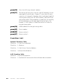
1
Model PCL-813
32-Channel Single-Ended
Isolated Analog Input Card
Copyright Notice
This documentation and the software included with this product are
copyrighted 1994 by Advantech Co., Ltd. All rights are reserved.
Advantech Co., Ltd. reserves the right to make improvements to the
products described in this manual at any time without notice.
No part of this manual or software may be reproduced, copied,
translated or transmitted, in any form or by any means without the
prior written permission of Advantech Co., Ltd. Information provided
in this manual is intended to be accurate and reliable. However,
Advantech Co., Ltd. assumes no responsibility for its use, nor for any
infringements of rights of third parties which may result from its use.
Acknowledgments
PC-LabCard is a trademark of Advantech Co., Ltd. IBM, PC and
PC/XT/AT are trademarks of International Business Machines
Corporation. MS-DOS, MASM, QuickBASIC, Microsoft C and MSPASCAL are trademarks of Microsoft Corporation. Intel is a trademark of Intel Corporation. Turbo C and Turbo PASCAL are trademarks of Borland International. MOXA is a trademark of 404
Technologies Inc.
Part No. 2003813030, 4th Edition
Printed in Taiwan, August, 1994
Contents
CHAPTER 1 INTRODUCTION ............................................... 1
Features ................................ 2
Specifications ............................ 3
General Specifications ....................... 3
CHAPTER 2 INSTALLATION ................................................ 5
InitialInspection .......................... 6
Switch and Jumper Settings ................... 7
Connector Pin Assignment .................... 9
Plugging the PCL-813 into your PC ............. 10
CHAPTER 3 SIGNAL CONNECTION .................................... 11
Analog Input Connection .................... 12
CHAPTER 4 REGISTER STRUCTURE
AND FORMAT ................................................ 13
I/O Port Address Map ......................
A/D Data Registers ........................
Gain Control Register ......................
Multiplexer Scan Register ...................
How to Initiate an A/D Conversion ..............
14
16
17
18
19
CHAPTER 5 SOFTWARE .................................................... 21
Introduction .............................
Parameter Table ..........................
Parameter Descriptions .....................
Function List ............................
Function Description .......................
Language Interface ........................
BASICA ...............................
GWBASIC (version 3.20) ...................
QuickBASIC 4.0 and 4.5 ....................
Microsoft C .............................
Turbo C ...............................
Borland C++ ............................
Microsoft PASCAL ........................
Turbo PASCAL ..........................
22
22
27
28
29
31
31
31
32
32
33
33
34
34
APPENDIX A CALIBRATION ................................................ 35
VR Assignments .......................... 36
VR location ............................. 37
A/D Calibration .......................... 38
APPENDIX B PCLD-881 INDUSTRIAL
TERMINATION BOARD ................................ 39
Introduction .............................
Features ...............................
Applications ............................
Technical Diagrams .......................
40
40
41
42
CHAPTER
INTRODUCTION
1
Chapter 1 Introduction
1
INTRODUCTION
The PCL-813 32 Channel Single-Ended Isolated Analog Input Card is
an easy to use and cost effective IBM PC/XT/AT compatible dataacquisition card. The specifications and the user-friendly software
driver of this card make it a popular solution for a wide range of
industrial and laboratory applications. Such applications include:
measurement of transducer and sensor data, waveform acquisition and
measurement, process monitoring, and vibration and transient
analysis.
Features
• 32 Single-ended, isolated analog inputs
• 12-Bit resolution A/D conversion
• Programmable analog input ranges: ±5 V, ±2.5 V, ±1.25 V, ±0.625 V,
0~10 V, 0~5 V, 0~2.5 V, 0~1.25 V
• Supports software trigger
• Versatile language drivers including BASIC, PASCAL, C and C++
2
PCL-813 User's Manual
Specifications
Analog Input (A/D Converter)
Channels
Channels: 32 Single-ended with isolation
Resolution
Resolution: 12-bit, successive approximation
Input Range
Range:
Bipolar: ±5 V, ±2.5 V, ±1.25 V, ±0.625 V, software programmable
Unipolar: 0 ~ 10 V, 0 ~ 5 V, 0 ~ 2.5 V, 0 ~ 1.25 V, software
programmable
(Bipolar or Unipolar is selected by JP100)
Converter
Converter: AD574 or equivalent, with 25 ms conversion time
rate: 25 Kbps maximum, software control only
Data transfer rate
Isolation voltage
voltage: >500 VDC from input to output
Accuracy
Accuracy: 0.01% of reading ±1 LSB
Nonlinearity
Nonlinearity: ±1 bit maximum
Amplification
Amplification: x1, x2, x4, x8, software programmable
Trigger mode
mode: By software trigger
Temp. coefficient
coefficient: ±25 ppm/OC
Overvoltage
Overvoltage: Continuous ±30 V maximum
impedance: >10 MW
Input impedance
General Specifications
Power consumption
consumption: +5 V: 660 mA, typical
+12 V: 140 mA, typical
I/O connector
connector: 37-pin D-type connector (analog input port)
Operating temp.
temp.: 0 to 50OC (32 to 122OF)
temp.: -20 to 50OC (-4 to 149OF)
Storage temp.
Board dimensions
dimensions: 99 mm x 219 mm
Weight
Weight: 210 gm (7.42 oz.)
Chapter 1 Introduction
3
CHAPTER
INSTALLATION
2
Chapter 2 Installation
5
INSTALLATION
Initial Inspection
When you receive your PCL-813 you should find enclosed:
• One PCL-813 32-Channel Single-Ended Isolated Analog Input Card
• User's Manual
• Utility Diskette, which includes the card's software driver
The PCL-813 was carefully inspected both mechanically and electrically before shipment. It should be free of marks and scratches and in
perfectelectricalorderonreceipt.
When unpacking, check the unit for signs of shipping damage
(damaged box, scratches, dents, etc). If there is damage to the unit or
it fails to meet specifications, notify our service department or your
local sales representative immediately. Also, call the carrier immediately and retain the shipping carton and packing material for the
inspection by the carrier. We will make arrangements to repair or
replacetheunit.
Remove the PCL-813 card from its protective packaging
carefully. Keep the anti-vibration package. Whenever you are not
using the board, please store it in the package for protection.
Discharge any static electricity by touching the back of the system
unit before you handle the board. You should avoid contact with
materialsthatcreatestaticelectricitysuchasplastic,vinyl,and
styrofoam. The board should be handled only by the edges to avoid
static electric discharge which could damage the integrated circuits on
the PCL-813.
Warning! Discharge your body’s static electric charge by
touching the back of the grounded chassis of the
system unit (metal) before handling the board. You
should avoid contact with materials that hold a static
charge such as plastic, vinyl and styrofoam. Handle
the board only by its edges to avoid static damage to
its integrated circuits. Avoid touching the exposed
circuit connectors.
6
PCL-813 User's Manual
Switch and Jumper Settings
The PCL-813 has been designed with ease-of-use in mind. On-board
the card you will notice that there is only one DIP switch (SW1). This
switch is used to set the PCL-813’s base address. Unipolar or Bipolar
mode inputs is selected by jumper JP100. The following section goes
intothisinmoredetail.
I/O Address Selection
Most peripheral devices and interface cards are controlled by your
PC’s I/O ports. These devices and cards should be placed in an
appropriate I/O space so that there will be no conflicts between them
and the PCL-813. Keep in mind that the PCL-813 uses 16 consecutive
address locations in your PC’s I/O space. The following table provides
an I/O port address map for your reference. This will assist in locating
appropriate addresses for your other peripheral devices and interface
cards. I/O port base addresses are selected from the 6-position DIP
switch SW1 on-board the PCL-813. The valid addresses are 000 to
3F0 (hexadecimal). The factory default base address setting is 220.
From time to time, you may find that you will have to use some of
these spaces for other devices. If this is the case, then you can change
the address according to the information given in the following table.
Chapter 2 Installation
7
CARD I/O Address (SW1)
I/O ADDRESS RANGE
1
(HEXADECIMAL)
A9
2
A8
SWITCH POSITION
3
4
5
A7
A6
A5
6
A4
000 - 100
l
l
l
l
l
l
100 - 10F
l
¡
l
l
l
l
------
-
-
-
-
-
-
------
-
-
-
-
-
-
200 - 20F
¡
l
l
l
l
l
* 210 - 21F
¡
l
l
l
l
¡
220 - 22F
¡
l
l
l
¡
l
------
-
-
-
-
-
-
300 - 30F
¡
¡
l
l
l
l
------
-
-
-
-
-
-
¡
¡
¡
¡
¡
¡
3F0 - 3FF
¡= Off
l = On
* = Factory default setting
NOTE: A4 through A9 corresponds to your PC’s address lines
Input Range Selection
If your application always uses Unipolar input types, you should
switch the JP100 to the “U” location, so the PCL-813 may accept to
0~10V, 0~5V, 0~2.5V and 0~1.25V Unipolar analog inputs.
8
PCL-813 User's Manual
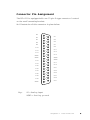
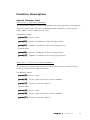
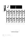
Connector Pin Assignment
The PCL-813 is equipped with one 37-pin D-type connector located
on the card’s mounting bracket.
An illustration of this connector is given below:
AI 0
1
AI 2
2
AI 4
AI 6
AI 8
AI 10
AI 12
AI 14
AGND
AGND
AI 16
AI 18
AI 20
AI 22
AI 24
AI 26
AI 28
AI 30
AGND
Key:
20
AI 1
21
AI 3
22
AI 5
23
AI 7
24
AI 9
25
AI 11
26
AI 13
27
AI 15
28
AGND
29
AGND
30
AI 17
31
AI 19
32
AI 21
33
AI 23
34
AI 25
35
AI 27
36
AI 29
37
AI 31
3
4
5
6
7
8
9
10
11
12
13
14
15
16
17
18
19
AI = Analog input
AGND = Analog ground
Chapter 2 Installation
9
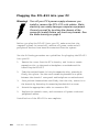
Plugging the PCL-813 into your PC
Warning! Turn off your PC’s power supply whenever you
install or remove the PCL-813 or its cables. Static
electricity can easily damage computer equipment.
Ground yourself by touching the chassis of the
computer (metal) before you touch any boards. See
the static warning on page 6.
Before you plug the PCL-813 into your PC, make sure that the
computer’s power is turned off, and that all power cords and all
peripheral devices have been disconnected from the system.
Use the following procedure as a guideline for plugging the PCL-813
into your PC.
1.
Remove the cover from the PC’s chassis, and locate a vacant
expansion slot on the passive backplane or motherboard for
installing the PCL-813.
2.
Take the card and insert it into the expansion slot, pressing it
firmly into place. Use the card’s mounting bracket as a guide
between the chassis’ rear panel and backplane or motherboard.
3.
Once you have inserted the card firmly into the slot, secure it to
the chassis by fastening its mounting bracket with a screw.
4.
Attach the appropriate cable to connector CN1.
5.
Replace the chassis cover, and reconnect all power cords and
peripheral cables.
Installation of the PCL-813 is now complete.
10
PCL-813 User's Manual
CHAPTER
3
Signal Connection
Chapter 3 Signal Connection
11
SIGNAL CONNECTION
Since most data acquisition applications involve voltage measurement,
it is important to make the correct signal connections in order to avoid
any damage to your system, and to ensure accurate measurements.
This chapter provides some helpful information about making the
proper signal connections for your application.
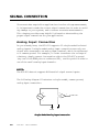
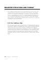
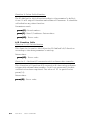
Analog Input Connection
As you already know, the PCL-813 supports 32 single-ended isolated
analog inputs. A single-ended analog input connection uses only one
signal wire connected to an analog input terminal, which is referenced
to a common ground. For example, in order to measure the voltage of
a battery, simply connect its negative side to the PCL-813’s ground
(any one of the AGND pins on connector CN1), and its positive side to
one of the card’s analog input channels.
NOTE:
The PCL-813 does not support differential signal source inputs.
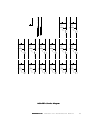
The following diagram illustrates a single-ended, common ground,
analog input connection:
+
2
Vs
1
To A/D CHIP
3
-
AGND
Single-Ended Analog Input Connection
12
PCL-813 User's Manual
CHAPTER
4
Register Structure
And Format
Chapter 4 Register Structure And Format
13
REGISTER STRUCTURE AND FORMAT
This chapter has been written for those who wish to write their own
software driver instead of using that of the PCL-813. The PCL-813
requires 16 consecutive addresses in I/O space. The most important
issue in programming the PCL-813 is understanding the meaning of
the 16 registers addressable from the selected I/O port base address.
Here, you will find detailed information about the PCL-813’s register
formats and control procedures.
I/O Port Address Map
The following table shows you which base I/O addresses are used by
the PCL-813. Refer to this map from time to time in order to become
familiar with each of the card’s register formats and their purpose.
Sixteen consecutive registers corresponding to their I/O addresses are
used to control the PCL-813’s various functions. The following table
has been provided in this chapter as a preface which outlines these
addresses, relative to their location and control (read or write) assignments.
14
PCL-813
User's Manual
I/O Port Address Map
LOCATION
BASE+0
READ
N/U
WRITE
N/U
BASE+1
N/U
N/U
BASE+2
N/U
N/U
BASE+3
N/U
N/U
BASE+4
A/D low byte
N/U
BASE+5
A/D high byte
N/U
BASE+6
N/U
N/U
BASE+7
N/U
N/U
BASE+8
N/U
N/U
BASE+9
N/U
Gain control
BASE+10
N/U
Multiplexer scan control
BASE+11
N/U
N/U
BASE+12
N/U
Software A/D trigger
BASE+13
N/U
N/U
BASE+14
N/U
N/U
BASE+15
N/U
N/U
NOTE
NOTE: N/U = Not used
The sections that follow provide further information about each
register’s data format according to its specific operation.
Chapter 4 Register Structure And Format
15
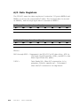
A/D Data Registers
The PCL-813 uses the data registers located at I/O ports BASE+4 and
BASE+5 to store the converted A/D data. The low byte data is stored
at BASE+4, and the high byte data is stored at BASE+5.
BASE+4 A/D Low Byte Data (Read)
D7
AD7
D6
AD6
D5
AD5
D4
AD4
D3
AD3
D2
AD2
D1
AD1
D0
AD0
D3
AD11
D2
AD10
D1
AD9
D0
AD8
BASE+5 A/D High Byte Data (Read)
D7
X
D6
X
D5
X
D4
DRDY
Where:
AD0 through AD11: Represent the PCL-813’s A/D data bits. AD0 is
the Least Significant Bit (LSB), and AD11 is the
Most Significant Bit (MSB).
DRDY:
16
PCL-813
Data Ready Bit. When A/D conversion is in
progress, this bit remains as 1. It becomes 0
when the A/D conversion is completed.
User's Manual
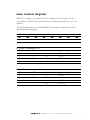
Gain Control Register
BASE+9 is used to set the PCL-813’s amplification gain for A/D
conversion. The PCL-813 provides four different gains: x1, x2, x4,
and x8.
The following tables outline BASE+9’s register format and corresponding gain settings:
BASE+9 Gain Control Register (Write)
D7
-
D6
-
D5
-
D4
-
D3
-
D2
-
D1
G1
D0
G0
If JP100 is located at B
G1
0
G0
0
Gain
x1
Input Range
±5 V
0
1
x2
±2.5 V
1
0
x4
±1.25 V
1
1
x8
±0.625 V
If JP100 is locatesd at U
G1
0
G0
0
Gain
x1
Input Range
0-10V
0
1
x2
0-5V
1
0
x4
0-2.5V
1
1
x8
0-1.25V
Chapter 4 Register Structure And Format
17
Multiplexer Scan Register
The PCL-813 can multiplex up to 32 channels of analog input. Users
have to set this register, located at BASE+10, to select the channel to
be measured before performing any A/D conversion. This is done by
selecting the channel to be used using a 5-bit register. The register
format is as shown below:
BASE+10 Multiplexer Scan Control (Write)
D7
-
D6
-
D5
-
D4
C4
D3
C3
D2
C2
D1
C1
D0
C0
In order to facilitate the selection of 32 channels using the 5-bit
register, each bit (D0~D4) can be set via the following table.
32 channel selection
18
C4
0
C3
0
C2
0
C1
0
C0
0
CH
0
0
0
0
0
1
1
0
0
0
1
0
2
0
0
0
1
1
3
0
0
1
0
0
4
0
0
1
0
1
5
0
0
1
1
0
6
0
0
1
1
1
7
0
1
0
0
0
8
.
.
.
.
.
.
.
.
.
.
.
.
1
1
1
1
1
31
PCL-813
User's Manual
How to Initiate an A/D Conversion
The PCL-813 A/D conversion is software controlled, and is based
upon the polling concept. After the A/D converter has been triggered,
the application program checks the Data Ready Bit (DRDY) of the A/
D status register. If this bit is detected (high), then A/D conversion is
in progress. When this bit returns to low, then A/D conversion is
completed, and the converted (binary) data may be read by the
program.
There are two software methods to force the A/D converter to execute
a single conversion: by writing a program yourself that writes the
instruction directly to the I/O port, or by writing a program which
utilizes that provided by the PCL-813 driver.
We suggest that you use the latter, the PCL-813 software driver, since:
• It makes your programming job easier.
• You will obtain a more readable source code which is easy to debug.
• It will enhance your program’s performance.
For those who prefer to use the first method, writing directly to the I/O
ports from within their own application, we provide the following step
by step procedure:
Step 1:
Set the desired channel by specifying the MUX scan range.
Wait at least 5 ms before issuing a new command to the
PCL-813.
Step 2:
Trigger the A/D conversion by writing any value to
BASE+12 of the A/D port, and then wait at least 20ms.
Step 3:
Wait until the Data Ready Signal (Read the A/D high byte
register DRDY bit, D4 of BASE+5) has returned to low.
Step 4:
Obtain the binary data by reading the A/D registers
(BASE+5 and BASE+4). First read the high byte, then the
low byte.
Step 5:
Convert the binary data to an integer value.
Refer to the DEMO01.C program for further details.
Chapter 4 Register Structure And Format
19
CHAPTER
Software
Chapter 5 Software
5
21
SOFTWARE
Introduction
This chapter describes the functions supported by the PCL-813
software driver. Programming languages supported by the driver
include BASICA, GWBASIC, Quick BASIC 4.0/4.5, Microsoft C,
Turbo C, Borland C++, Microsoft PASCAL, and Turbo PASCAL. The
driver is a Terminate and Stay Resident (TSR) program which runs
in the background while your application runs in the foreground. You
must install the driver before you can use the following functions.
Each PC-LabCard has its own driver, loaded by typing the appropriate
filename at the DOS prompt. In the case of the PC-LabCard PCL-813,
just type “PCL-813” at DOS prompt, and press enter to load the
program.
Parameter Table
The software driver simplifies your programming by using a Parameter Table reference algorithm. The tables hold parameters, minimum
and maximum values, and other specific information regarding the
functions. In contrast, the application program contains tables
specifying parameters and modes of operations. All the function calls
supported by the drivers need only two arguments: the function
number and a memory address pointer which points to a pre-defined
Parameter Table.
Once the Parameter Table is defined, just assign the desired function
number and the Parameter Table’s address to the driver. Once this is
done, it will pick up the necessary parameters associated with that
specific function call, and then automatically execute the function.
A Parameter Table’s format will be illustrated in detail later in this
manual. What you have to know here is that the Parameter Table
includes all the parameter settings necessary for all data acquisition
function calls supported by the software driver. The following is an
example of parameter tables:
22
PCL-813
User's Manual
Example (C language):
extern pcl813(int, unsigned int *);
unsigned param[60];
/* Parameter Table */
unsigned buffer[100];
/* A/D data buffer */
main()
{
unsigned far *ptr;
/* buffer pointer */
tr = (unsigned far *) buffer;
param[0] = 0;
/* card number
*/
param[1] = 0x220;
/* I/O base address */
param[10] = FP_OFF(ptr);
/* offset address
*/
param[11] = FP_SEG(ptr);
/* segment address */
param[12] = 0;
/* only one buffer used
*/
param[13] = 0;
param[14] = 100;
/* number of A/D conversion */
param[15] = 0x0;
/* A/D start channel*/
param[16] = 0xA;
/* A/D stop channel */
param[17] = 0x0;
/* gain code
*/
pcl813(3,param);
pcl813(4,param);
pcl813(5,param);
/* initialize the PCLabCard */
/* initialize A/D func
tion
*/
/* A/D conversions, and
store*/
/* converted data to
buffer */
.
.
}
Chapter 5 Software
23
There are two ways to change your program’s settings:
1. Modify corresponding parameters directly.
If you want to change the A/D start channel number, for example, you
do not need to issue any function calls to change this setting, just
change the corresponding parameter in your Parameter Table.
Example (C language):
extern pcl813(int, unsigned int *);
unsigned int param[60];/* Parameter Table*/
main()
{
.
.
.
param[15] = 0x0;
param[16] = 0xA;
pcl813(5,param);
.
.
param[15] = 0x2;
pcl813(5,param);
.
.
}
24
PCL-813
User's Manual
/* A/D start channel
/* A/D stop channel
/* S/W triggered A/D
conversion
*/
/* A/D start channel
/* S/W triggered A/D
conversion
*/
*/
*/
*/
2. Create a new Parameter Table.
The software driver’s job-oriented algorithm gives your program the
capability of addressing several Parameter Tables using the same
function call or group of function calls in one program. It should be
noted, however, that the driver can only address one Parameter Table
at a time. The driver executes the jobs according to the specified
Parameter Table. For convenient programming, we can define an
individual Parameter Table in advance for each of frequently called
functions without troublesome table modifications.
Example (C language):
extern pcl813(int, unsigned int *);
unsigned param1[60];/* Parameter Table 1 */
unsigned param2[60];/* Parameter Table 2 */
main()
{
.
.
.
/* JOB 1 */
param1[15] = 0x0;
param1[16] = 0xA;
param1[17] = 0x0;
pcl813(5,param1);
.
.
.
/* JOB 2 */
param2[15] = 0x2;
param2[16] = 0x8;
param2[17] = 0x5;
pcl813(5,param2);
*/
.
.
.
}
/*
/*
/*
/*
A/D start channel
*/
A/D stop channel
*/
gain code
*/
S/W triggered A/D conversion */
/*
/*
/*
/*
A/D start channel
*/
A/D stop channel
*/
gain code
*/
S/W triggered A/D conversion
Chapter 5 Software
25
Two Parameter Tables are defined in this example, Jobs 1 and 2 are
the same, except for the start channel, stop channel and gain setting.
NOTE:
1). When using BASIC language, negative numbers must be used to
represent integer data over 32767.
2). Negative number = integer - 65536.
3). For example, you need to pass 45000 as a input parameter to
BASIC function: 45000 - 65536 = -20536. So you have to use 20536 rather than 45000 as a parameter for the BASIC function.
Parameter List
26
Name
Board number
Size
1 word
Index
Param[0]
Base I/O address
1 word
Param[1]
Reserved
1 word
Param[2]
Reserved
1 word
Param[3]
Reserved
1 word
Param[4]
Reserved
2 words
Param[5]
Reserved
1 word
Param[7]
Reserved
1 word
Param[8]
Reserved
1 word
Param[9]
A/D Data Buffer A’s address
2 words
Param[10]
A/D Data Buffer B’s address
2 words
Param[12]
A/D conversion number
1 word
Param[14]
A/D start channel
1 word
Param[15]
A/D stop channel
1 word
Param[16]
Overall gain code
1 word
Param[17]
Gain code array pointer
2 words
Param[18]
Error number
1 word
Param[45]
Return value 0
1 word
Param[46]
Return value 1
1 word
Param[47]
PCL-813
User's Manual
Parameter Descriptions
param[0]
0 = Specify Number one Card.
1 = Specify Number two Card.
The software driver supports up to two PC-LabCards at
one time. Set Param[0] to tell the driver which card is
specified.
param[1]
PC-LabCard I/O address can be anywhere from 200
(Hex) to 3F0 (Hex). The base address can be set to 200
or 210, 230 or 240 .... 3F0.
param[10] Offset address for A/D data buffer A.
param[11] Segment address for A/D data buffer A.
param[12] Offset address for A/D data buffer B.
param[13] Segment address for A/D data buffer B.
NOTE:
For C or PASCAL, use their built-in memory allocation
functions to allocate sufficient memory for buffers A and B. These
memory allocation functions will return the offset and segment
addresses. Save them to Param[10] through Param[13]. If buffer B is
not used, be sure that you set Param[12] and Param[13] to 0.
Because BASICA and Quick BASIC do not provide memory allocation functions, you will have to assign explicit segment addresses for
each buffer. If you assign a segment address as 0, then the driver will
use the current data segment (DS) for buffers A and B. If buffer B is
not used, be sure that you set Param[12] and Param[13] to 0.
param[14] This parameter sets the A/D conversion number. The
range is from 1 to 32767.
param[15] Sets the A/D start channel number.
Chapter 5 Software
27
param[16] Sets the A/D stop channel number.
param[17] The driver allows you to set all the A/D channels to the
same amplification gain. Param[17] sets the A/D gain
code for all channels. Remember that individual amplifi
cation gains can be set for each channel, defined in the
gain array table. This parameter is used only for setting
all A/D channels to the same amplification gain. Set
Param[17] to FF (Hex) to cause the driver to refer to
the gain array table.
param[18] Offset address for the gain array table.
param[45] Error number.
param[46] Return value 0.
param[47] Return value 1.
Function List
Special Function Calls
Function 0: Get Error Message.
Function 1: Reserve.
Function 2: Get Driver Version Number.
Function 3:DriverInitialization.
A/D Function Calls
Function 4:A/DInitialization
Function 5: Perform A/D conversion with software data transfer.
28
PCL-813
User's Manual
Function Description
Special Function Calls
Function 0 : Get Error Message.
This function returns a zero-terminated text string pointer corresponding to an error code. The zero-terminated text string is a text string
with numeric zero added at the end.
Parameters used:
param[45]
param[45]: Error code.
param[46]
param[46]: Offset of address of the string pointer.
param[47]
param[47]: Segment of address of the string pointer.
Return data:
param[46]
param[46]: Offset of address of the string pointer.
param[47]
param[47]: Segment of address of the string pointer.
Function 2 : Get Driver Version Number.
This function returns the current version of the driver as well as the
version of this Driver Specification.
Parameters used:
param[45]
param[45]: Error code.
param[46]
param[46]: Driver specification version number.
param[47]
param[47]: Driver version number.
Return data:
param[45]
param[45]: Error code.
param[46]
param[46]: Driver specification version number.
param[47]
param[47]: Driver version number.
Chapter 5 Software
29
Function 3: Driver Initialization.
The PC-LabCard is initialized according to the parameter’s definitions. It will stop all functions and release all resources. It should be
called before any other function.
Parameters used:
param[0]
param[0]: Board number.
param[1]
param[1]: Base I/O address. Return data.
param[45]
param[45]: Error code.
A/D Function Calls
Function 4 : A/D Initialization
This function is used to initialize the PC-LabCard’s A/D function
according to the above parameter’s setting.
Return data:
param[45]
param[45]: Error code.
Function 5 : Perform A/D conversion with software data transfer.
This function will perform A/D conversion N times using software
trigger with software data transfer. It will not return until the Nth.
conversion has been completed. The value of ‘N’ is specified at
param[14].
Return data:
param[45]
param[45]: Error code.
30
PCL-813
User's Manual
Language Interface
BASICA
The following program example provides you with the appropriate
procedures to load the language interface for BASICA and GWBASIC
version 2.02.
Example:
100
CLEAR 49152!
110
DEF SEG = 0
120
SEG = 256 * PEEK(&H511) + PEEK(&H510)
130
SG = SG + 49152! / 16
140
DEF SEG = SG
150
BLOAD “813BAS.BIN”, 0
GWBASIC (version 3.20)
The following program example provides you with the appropriate
procedures to load the language interface for GWBASIC Version 3.20
andlater.
Example:
110
‘LOAD 813BAS.BIN DRIVER TO AN OUTSIDE AREA
120
DEF SEG= &H5000’DEFINE OUTSIDE AREA
130
BLOAD “813BAS.BIN”
140
‘END OF DRIVER LOADING
Chapter 5 Software
31
QuickBASIC 4.0 and 4.5
The following program example provides you with the appropriate
procedures to load the language interface for QuickBASIC 4.0 or 4.5.
Example 1:
QB filename /L 813QB.QLB
Example 2:
QB /L 813QB.QLB
Microsoft C
The following examples show you how to compile and link the
interface for different modes using Microsoft C.
Small Mode:
Compile :cl/AS/cfile.c
Link
Compact Mode:
Compile :cl/AC/cfile.c
Link
Medium Mode:
PCL-813
: link file+813CM.LIB;
Compile :cl/AL/cfile.c
Link
32
: link file+813CC.LIB;
Compile :cl/AM/cfile.c
Link
Large Mode:
: link file+813CS.LIB;
User's Manual
: link file+813CL.LIB;
Turbo C
The following examples show you how to compile and link the
interface for different modes using Turbo C.
DOS Command Line
Small Mode
:
TCC -ms file.c 813cs.lib
Compact Mode
:
TCC -mc file.c 813cc.lib
Medium Mode
:
TCC -mm file.c 813cm.lib
Large Mode
:
TCC -ml file.c 813cl.lib
Integrated Development Environment
You will need to use a general text editor to create a project file with
the extension name “PRJ”, for example 813.PRJ, which contains the
corresponding mode interface and your program list.
Small Mode
:
The project file should contain 813cs.lib
Compact Mode
:
The project file should contain 813cc.lib
Medium Mode
:
The project file should contain 813cm.lib
Large Mode
:
The project file should contain 813cl.lib
Borland C++
The following examples show you how to compile and link the
interface for different modes using Borland C++.
DOS Command Line
Small Mode
:
BCC -ms -c file.c 813cs.lib
Compact Mode
:
BCC -mc -c file.c 813cc.lib
Medium Mode
:
BCC -mm -c file.c 813cm.lib
Large Mode
:
BCC -ml -c file.c 813cl.lib
Integrated Development Environment
In Borland C++’s integrated environment, just pick the “Project”
menu to create a project file and add the corresponding mode interface
toit.
Chapter 5 Software
33
Microsoft PASCAL
The following examples show you how to compile and link the
language interface using Microsoft PASCAL.
Example:
Compile : pas1 demoxx pas2
Link
: link demoxx,,,813msp+pascal;
Turbo PASCAL
The following examples show you how to compile and link the
language interface using Turbo PASCAL by adding certain statements
to your program.
Example 1:
rogram main;
uses Crt;
{$F+}
{$L 813tpf} { use as far call }
Example 2:
rogram main;
uses Crt;
{$F-}
{$L 813tpn} { use as near call }
34
PCL-813
User's Manual
APPENDIX
A
Calibration
APPENDIX A Calibration
35
CALIBRATION
In data acquisition and control applications, it is important to ensure
that all measurement devices are calibrated regularly in order to
maintain accuracy. A calibration program, CALB.EXE, is provided on
the PCL-813 software disk to assist your calibration work.
The minimum equipment required to perform a satisfactory calibration is a 4½ digit digital multimeter. In addition, a voltage calibrator or
stable DC voltage source is required. A card-extender, such as the PCLabCard Model PCL-757, is an inexpensive device that you will find
greatly improves access to the board during calibration and will
probably be useful for other applications.
Calibration is easily performed using the CALB.EXE program. This
program will lead you through the calibration and set-up procedure
with a variety of prompts and graphic displays directing you to the
appropriate adjustments. Material in this section is brief and is
intended for use in conjunction with the calibration program.
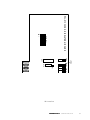
VR Assignments
The PCL-813 has four on-board VRs, which will allow you to make
accurate calibration adjustments for each of the card’s A/D functions.
The location of each VR is indicated in Figure A-1. The function of
each VR is listed below:
36
VR1
A/D Bipolar offset adjustment
VR2
A/D Bipolar full-scale adjustment
VR3
Programmable amplifier offset adjustment
VR4
A/D Unipolar full-scale adjustment
PCL-813
User's Manual
PCL-813 32 CH S.E ISOLATED A/D CARD
(A987 654)
SW1
TP 1
VR1 VR2 V
U 19
JP 100
VR4
U 21
VR Location
37
APPENDIX A Calibration
A/D Calibration
Because the PCL-813 supports a variety of A/D input ranges, accurate
calibration for a certain A/D range may result in a small offset when
the input range is altered. It is strongly suggested that you recalibrate
whenever a different A/D range is selected.
Calibration Steps:
a. Bipolar Adjustment: (JP100 located at “B”)
(1)
Short the A/D input of Channel 0 to AGND. Adjust VR1
until the reading of the A/D conversion flickers between
2047 and 2048.
(2)
Apply a voltage with a full-scale value corresponding to the
specific A/D input range to A/D Channel 0. Adjust VR2
until the reading of the A/D conversion flickers between
4094 and 4095.
b. Unipolar Adjustment: (JP100 located at “U”)
38
(1)
Short the A/D input of channel 0 to AGND. Adjust VRI
until the reading of the A/D conversion flickers between
0000 and 0001.
(2)
Apply a voltage with a full-scale value corresponding to the
specific A/D input range to A/D channel 0. Adjust VR4
until the reading of the A/D conversion flickers between
4094 and 4095.
PCL-813
User's Manual
APPENDIX
B
INDUSTRIAL
TERMINATION
BOARD
APPENDIX B Industrial Termination Board
39
Introduction
The PCLD-881 is an universal screw terminal board designed for feild
signal wiring in industrial applications. It can be connected to the
analog and digital ports of various PC-LABCards via shielded cable
and DB-37 connector.
Due to the PCLD-881's special PCB layout you can install passive
components to construct your own signal-conditioning circuits. You
can easily construct a low-pass filter, attenuator or current-to-voltage
converter by adding resistors and capacitors onto the board’s circuit
pads.
Features
• Low-cost universal screw-terminal board for PC-LabCards with 20pin connectors
• 40 terminal points for one DB-37 port
• Reserved space for signal-conditioning circuits such as low-pass
filter, current shunt and voltage attenuator
• Industrial type termination blocks permit heavy-duty and reliable
connections of signals
• Table-top mounting using nylon standoffs. Screws and washers
provided for panel or wall mounting
• Dimensions: 8.7" (L) x 4.53" (W) (221 mm x 115 mm)
40
PCL-813 User's Manual
Applications
• Field wiring for analog and digital I/O channels of PC-LabCards
which employ standard or DB-37 connectors
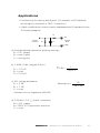
• Signal-conditioning circuits can be implemented as illustrated in the
following examples:
Ra
AIO
Internal
connector
Rb
Terminal
block
C0
A GND
a) Straight-through connection (factory setting):
Ra = 0 W jumper
Rb = none (open)
C0 = none(open)
b) 1.6 KHz (3 dB) low pass filter:
f 3 dB =
Ra = 10 KW
Rb = none
Co = 0.01 mF
1
2pRaC0
c) 10:1 voltage attenuator:
Ra = 9 KW
Rb = 1 KW
C0 = none
Attenuation =
Rb
Ra + Rb
(Assume source impedance «10 KW )
d) 4-20 mA to 1-5 VDC signal converter:
Ra = 0 W jumper
Rb = 250 W (0.1% precision resistor)
C0 = none
APPENDIX B Industrial Termination Board
41
CN1
1
AI1
AI0
AI3
AI2
AI4
2
3
20
AI6
AGND
AI7
CD7
CAP
CD8
21
CAP
AGND
AI5
AI9
AI6
AI10
AI7
AI11
AI8
AI8
24
AI12
22
6
AI13
4
25
AI14
5
7
23
8
26
RD13
R
RD14
R
RD15
R
RD16
R
RD17
R
RD18
EI6
AGND
EI7
AGND
EI8
AI0
AGND
AI1
AGND
AI2
CD1
CAP
CD2
CAP
CD3
RD2
R
RD4
R
RD6
RD1
R
RD3
R
RD5
AGND
R
AGND
R
AI16
CAP
28
AI17
AGND
10
AI18
AGND
29
AI19
R
11
AI20
CD9
30
AI21
CD10
CAP
AGND
12
CAP
AI15
31
AI22
AGND
13
AI23
AGND
32
AI24
9
14
AI25
27
33
AI26
R
AGND
AI10
RD20
R
RD21
AGND
EI10
AGND
AI4
AGND
CAP
CD5
CAP
CD6
CAP
R
R
R
RD9
Size
Title
RD11
R
RD12
R
RD7
15
AI27
R
RD19
34
AI28
AGND
AI5
AGND
RD8
16
AI29
R
EI11
AGND
AI3
35
AI30
RD10
CAP
RD23
R
RD24
R
EI9
17
RD22
AGND
R
36
AI31
AI9
18
AGND
CD12
CAP
CD4
37
AI11
AGND
CD11
19
CONNECTOR DB37
AGND
AI[12..31]
EI[12..31]
EI
AG
EI
AG
EI
AG
EI
AG
EI
AG
EI
AG
Doc
PCL-813 User's Manual
42
AI[12..31]
EI[12..31]
PCLD-881 Circuit Diagram
AI30
AGND
AI31
AGND
AI[12..31]
EI[12..31]
AGND
CD31
CAP
CD32
CAP
AI24
RD49
R
EI24
AGND
EI25
AGND
EI26
AGND
EI27
AGND
AI18
AGND
AI19
AGND
AI20
AGND
AI21
AGND
AI22
AGND
EI28
AGND
AI23
AGND
EI29
AGND
CD19
CAP
CD20
CAP
CD21
CAP
CD22
CAP
CD23
CAP
CD24
CAP
RD3
R
RD38
R
RD3
R
RD40
R
RD4
R
RD42
R
RD4
R
RD44
R
RD4
R
RD46
R
RD4
R
RD48
R
43
APPENDIX B Industrial Termination Board
RD61
EI30
R
R
CD25
CAP
R
AGND
RD51
RD50
AGND
AI25
RD62
R
RD63
EI31
R
R
R
R
RD60
R
RD59
RD58
R
RD57
RD56
R
RD55
RD54
R
R
CD26
CAP
CD27
CAP
CD28
CAP
CD29
CAP
CD30
CAP
RD53
R
AGND
RD52
AGND
AGND
AI27
AGND
AI26
RD64
R
AI[12..31]
EI[12..31]
AI28
AGND
AI29
AGND
PCLD-881 Circuit Diagram
APPENDIX
CALIBRATION
In data acquisition and control applications,
it is important to ensure that all measurement
devices are calibrated regularly in order to
maintain accuracy. A calibration program,
CALB.EXE, is provided on the PCL-813 software
disk to assist your calibration work.
The minimum equipment required to perform a
satisfactory calibration is a 4½ digit digital
multimeter. In addition, a voltage calibrator
or stable DC voltage source is required. A
card-extender, such as the PC-LabCard Model
PCL-757, is an inexpensive device that you will
find greatly improves access to the board during calibration and will probably be useful for
other applications.
Calibration is easily performed using the
CALB.EXE program. This program will lead you
through the calibration and set-up procedure
with a variety of prompts and graphic displays
directing you to the appropriate adjustments.
Material in this section is brief and is intended for use in conjunction with the calibra-
tion program.
VR Assignments
The PCL-813 has four on-board VRs, which will
allow you to make accurate calibration adjustments for each of the card’s A/D functions. The
location of each VR is indicated in Figure A-1.
The function of each VR is listed below:
VR1
A/D Bipolar offset adjustment
VR2
A/D Bipolar full-scale adjustment
VR3
adjustment
Programmable amplifier offset
VR4
ment
A/D Unipolar full-scale adjust-
Figure A-1 VR Location
A/D Calibration
Because the PCL-813 supports a variety of A/D
input ranges, accurate calibration for a certain A/D range may result in a small offset
when the input range is altered. It is strongly
suggested that you recalibrate whenever a different A/D range is selected.
Calibration Steps:
a. Bipolar Adjustment: (JP100 located at “B”)
(1)
Short the A/D input of Channel 0 to
AGND. Adjust VR1 until the reading of the A/D
conversion flickers between 2047 and 2048.
(2)
Apply a voltage with a full-scale value
corresponding to the specific A/D input range
to A/D Channel 0. Adjust VR2 until the reading
of the A/D conversion flickers between 4094 and
4095.
b. Unipolar Adjustment: (JP100 located at “U”)
(1)
Short the A/D input of channel 0 to
AGND. Adjust VRI until the reading of the A/D
conversion flickers between 0000 and 0001.
(2)
Apply a voltage with a full-scale value
corresponding to the specific A/D input range
to A/D channel 0. Adjust VR4 until the reading
of the A/D conversion flickers between 4094 and
4095.
PCLD-881
Industrial Terminal Board