1
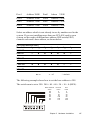
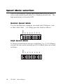
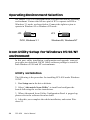
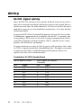
PCL-858
8-Port RS-232
Interface Card
Copyright Notice
This documentation and the software included with this product are
copyrighted 2001 by Advantech Co., Ltd. All rights are reserved.
Advantech Co., Ltd. reserves the right to make improvements to the
products described in this manual at any time without notice.
No part of this manual or software may be reproduced, copied,
translated or transmitted, in any form or by any means without the
prior written permission of Advantech Co., Ltd. Information provided in this manual is intended to be accurate and reliable. However,
Advantech Co., Ltd. assumes no responsibility for its use, nor for any
infringements of rights of third parties which may result from its use.
Acknowledgments
PC-LabCard is a trademark of Advantech Co., Ltd. IBM, PC and
PC/XT/AT are trademarks of International Business Machines
Corporation. MS-DOS, MASM, QuickBASIC, Microsoft C and MSPASCAL are trademarks of Microsoft Corporation. Intel is a trademark of Intel Corporation. Turbo C and Turbo PASCAL are trademarks of Borland International.
Part No. 2000085801 2nd Edition
Printed in Taiwan May 2001
Contents
Chapter 1: Introduction ................................................... 5
Description ............................................................................. 6
Features .................................................................................. 7
Specifications ......................................................................... 7
Chapter 2: Hardware Installation .................................. 11
Initial Inspection ................................................................. 12
Card Configuration ............................................................ 14
Default Settings ................................................................... 14
I/O Address and Interrupt Setup ...................................... 14
Speed Mode selection .......................................................... 18
Chapter 3: Software Installation ................................... 19
Operating Environment Selection ..................................... 20
Icom Utility Setup for Windows 95/98/NT environment . 20
Chapter 4: Wiring ........................................................... 23
Connector Pin Assignments ............................................... 24
Wiring .................................................................................. 26
Appendix A: PC I/O Address Reference ......................... 29
PC I/O Address Usage ........................................................ 30
Appendix B: Quick Reference ........................................ 31
CHAPTER
Introduction
1
Chapter 1 Introduction
5
Description
The PCL-858 series are eight ports serial communication interface
card. The PCL-858A/858B serial ports are implemented using
16C554 UARTs which makes serial I/O more reliable.
The PCL-858 series support all eight ports can be set the address
automatically. All channels share the same interrupt (IRQ), and
interrupt status register is available for determining the interrupt
source. When an on-board interrupt occurs the interrupt status register
(vector address) indicates which port has generated it. The shared
interrupt can be set to most common (extended) AT interrupts. This
simplifies programming, speeds up interrupt processing and frees up
interrupts for other devices.
The PCL-858 series developed by Advantech Co., Ltd has passed the
CE test for environmental specifications.
6
PCL-858
User's Manual
Features
v
Eight independent RS-232 serial ports
v
Transmission speed up to 921.6Kbps
v
Independent I/O address, Share IRQ setting for each of 8 serial ports
v
Wide IRQ selection: 3, 4, 5, 6, 7, 9, 10, 11, 12, 15
v
Supports DOS/Windows 3.1 (PC-ComLib), Windows 95/98, Windows NT
v
Supports surge protection : 3000 VDC (PCL-858B)
v
PC-ComLib, Icom Utility software included
Specifications
l
Bus interface: ISA
l
Number of ports: 8
l
I/O address: 0x0000 ~ 0x03F8
l
IRQ: 3, 4, 5, 6, 7, 9,10, 11, 12, 15
l
Data bits: 5, 6, 7, 8
l
Stop bits: 1, 1.5, 2
l
Parity: none, even, odd
l
UART:
2 x 16C554 (PCL-858A/858B)
l
Speed (bps): 50 ~ 921.6K
l
Data signals: TxD, RxD, RTS, CTS, DTR, DSR, DCD, RI, GND
l
Surge protection: 3000VDC (PCL-858B)
Chapter 1 Introduction
7
l
Power requirement: 450mA typical 950 A max. (+5V),
140mA typical. 240mA max.((12V),
l
Dimensions: 18.5cm x 10.0cm
l
Operating Temperature.: 0 ~ 60°C (refer to IEC-68-1.2.3 item)
l
Storage Temperature: -25 ~ 80°C
l
MTBF:
over 99,100 hrs (PCL-858A) at 25°C, Ground, fixed, environment
over 92,363 hrs (PCL-858B) at 25°C, Ground, fixed environment
l
For technical support and service please visit our support website
at:
http://support.advantech.com
and visit the “Industrial Automation Support” and “FAQ” sections
8
PCL-858
User's Manual
Chapter 1 Introduction
Figure 1-1: Switch and jumper layout
9
10
PCL-858
User's Manual
CHAPTER
Hardware
Installation
2
Initial Inspection
Depending on the option you ordered, in addition to this manual, you
should find the following items inside the shipping container:
• PCL-858(A/B) 8-port RS-232 Card
• One diskette with Icom Utility software
• One PCL-858 manual
We have carefully inspected the PCL-858 mechanically and electrically before shipping. It should be free of marks and scratches and in
perfect working order on receipt.
As you unpack the PCL-858, check it for signs of shipping damage
(damaged box, scratches, dents, etc.). If it is damaged or it fails to
meet specifications, notify our service department or your local sales
representative immediately. Also notify the carrier. Retain the
shipping carton and packing material for inspection by the carrier.
After inspection we will make arrangements to repair or replace the
unit.
Remove the PCL-858 from its protective packaging by grasping the
rear metal panel. Keep the anti-vibration packing. Whenever you
remove the card from the PC, store it in this package for protection.
Warning! Discharge your body’s static electric charge by
touching the back of the grounded chassis of the
system unit (metal) before handling the board. You
should avoid contact with materials that hold a static
charge such as plastic, vinyl and styrofoam. Handle
the board only by its edges to avoid static damage to
its integrated circuits. Avoid touching the exposed
circuit connectors.
12
PCL-858
User's Manual
Chapter 2 Hardware Installation
13
Card Configuration
The DIP switch sets the port to the appropriate I/O address and speed
mode. The jumpers set the port's IRQ.
Default Settings
The board is shipped with default settings. If you need to change
these settings, however, see the following sections. Otherwise, you
can simply install the card. Note that you will need to disable your
CPU card's on-board COM ports, if any, or set them to alternate
addresses / IRQs. (Note: The function of JP2 doesn't offer to user, only
for manufacture.)
PCL-858 Default Configuration
Setting
JPI
Default function
IRQ 12
Speed mode
1x
Base address
Address 300H
Vector address
Interrupt 280H
I/O Address and Interrupt Setup
Next, you will need to select an IRQ (interrupt request) number, and
an I/O base address for the PCL-858.
Base address setting (SW1)
For base address specify the I/O address of the first port and subsequent ports are set continuous base addresses by the offset of 8 bytes.
For instance, if the first port is set for 300H, then the second port is set
to 308H sequentially. For PORT number, specify the continuous
PORT number of the first port and subsequent ports are mapped to
continuous PORT numbers. For example:
14
PCL-858
User's Manual
Port 1
Address 300H
Port5
Adress 320H
Port 2
Address 308H
Port 6
Address 328H
Port 3
Address 310H
Port 7
Address 330H
Port 4
Address 318H
Port 8
Address 338H
Select an address which is not already in use by another card in the
system. If you are installing more than one PCL-858 card in your
system, set the card to different base address. DIP switch(SW1)
controls each card’s base address, as shown below.
Port base address (SW1)
Base Address
200-21F
A3
A4
A5
A6
A7
A8
A9
l
l
l
l
l
l
¡
208-227
¡
l
l
l
l
l
¡
¡
l
¡
¡
¡
l
¡
l
l
l
l
l
¡
¡
l
l
¡
¡
¡
¡
¡
··········
2E8-307
··········
*300-31F
··········
3E0-3FF
l: on
¡ : off
*= default
The following example shows how to set the base address to 2F8.
The switch sum is set to 2F8: 200 + 80 + 40 + 20 + 10 + 8 (HEX).
Base Address
Value
Decimal
Value
Hex
Value
A9
A8
A7
A6
A5
A4
A3
8
16
32
64
128
256
512
8
10
20
40
80
100
200
A9
A8
A7
A6
A5
A4
A3
Chapter 2 Hardware Installation
15
IRQ Setting (JP1)
All channels in PCL-858 series share the same interrupt (IRQ), and
interrupt status register is available for determining the interrupt
source. Select an IRQ which is not already in use by another card in
the system. If you are installing more than one PCL-858, set them to
different IRQ number. Jumper Bank JP1 controls the card IRQ. Simply
place the jumper on the interrupt level as shown in the following
figure.
15 12 11 10 9
7
6
5 4
3
Interrupt status register setup (SW2, Vector
address)
When data arrives at one of the eight ports, it will generate an
interrupt in the interrupt register. The software can read this, and
identify immediately which port generated the interrupt. This save
time, and makes programming easier. In DOS and Windows 3.1
environment, when a data bit of the interrupt status register is set to 0,
the corresponding channel is select to generate an interrupt, and vice
versa for Windows 95/98/NT system. If the bit is 1, then no interrupt
status register, and vice versa for Windows 95/98/NT system, as shown
in the following figure and table.
A9
A8
A7
A6
A5
User's Manual
A4
PCL-858
A3
Speed
16
Interrupt Status Register SW2
Bit
Function
0
Port1
1
Port2
2
Port3
3
Port4
4
Port5
5
Port6
6
Port7
7
Port8
The user may change the interrupt status address via SW2. Please note
the address decorder will occupy a continuous, 8-bytes area related to
switch setting. For example, if you set the switch to 210H, then the
address 210H to 217H will all be decoded. The various DIP switch
setting (SW2) for the interrupt status register are shown in the table.
Vector Address (SW2)
A3
A4
A5
A6
A7
A8
A9
200H
l
l
l
¡
¡
¡
¡
210H
l
¡
l
l
l
l
¡
l
¡
l
¡
l
l
¡
l
l
l
l
l
¡
¡
l
¡
¡
¡
¡
¡
¡
··········
250H
··········
300H
··········
3F0H
l: on
¡ : off
Chapter 2 Hardware Installation
17
Speed Mode selection
The PCL-858 employs a unique speed option that allows the user to
choose either normal speed mode (1x) or high speed mode (8x). This
high speed mode is selected at SW2.
Normal Speed Mode
To select the baud rate commonly associated with COM ports , such
as 2400, 4800, 9600. . .115.2 Kbps, place the switch as follows.
A9
A8
A7
A6
A5
A4
A3
SPEED
High Speed Mode
To increase normal mode rates up to eight times, (e.g. if 115.2 Kbps is
selected, the rate can be increased up to 921.6 Kbps), place the switch
as follows.
A9
A8
A7
A6
A5
User's Manual
A4
PCL-858
A3
SPEED
18
CHAPTER
Software
Installation
3
Operating Environment Selection
Set jumper 3 (JP3) to correspond with your desired software operating
environment. Connect the left two pins of JP3 to operate in DOS or
Windows 3.1 mode, as shown below. Connect the right two pins to
operate in Windows 95 or Windows NT mode .
1
JP3
JP3
DOS, Windows 3.1
1
Windows 95, Windows NT
Icom Utility Setup for Windows 95/98/NT
environment
In this part, utility installation, configuration and upgrade/ removal
procedure are described. IOCM Utility software package is stated for
both Windows 95/98 and NT environments.
.
Utility Installation
The following is the procedure for installing PCL-858 under Windows
95/NT:
1. Run Setup.exe in the driver diskette.
2. Select “Advantech Icom Utility” to install and configure the
boards following the on-line instructions.
3. When Advantech Icom Utility Configuration Panel is popped up,
please refer to the software for more detail.
4. After this, user complete the whole installation, and restart Windows 95.
20
PCL-858
User's Manual
Up to now, users have already completed the whole installation,
please restart system as prompted.
Once the board and driver are installed and the system restart
successfully, users can execute any ready-made application such as
HyperTerminal to transmit/receive data or Remote Access Service
to provide dial-up networking capability.
Configuration:
You will enter the configuration program when installing the device
driver. Or you can click on the Taskbar [Start] button, then select
[Programs] menu, then [Advantech Icom Utility] menu and then
[Icom] icon.
When the configuration panel is popped up:
Click [Add Board] button to add a board.
Click [Delete] button to remove a board.
Board Type: PCL-858
Base COM: Specify the COM number of the first port and subsequent
ports are mapped to continuous COM numbers. For instance, if the
first port is mapped to COM10, then the second port is mapped to
COM11 sequentially.
Base Address (200H~3F8H): Specify the base address of the first port
and subsequent base address are mapped to continuous COM
numbers. For instance, if the first port is mapped to 300H, then the
second port is mapped to 308H sequentially.
Chapter 3 Software Installation
21
At PCL-858 series can be installed together as long as the memory
resources are sufficient and available in a system. The board can share
only one same IRQ, and different board will set different IRQ.
Click [Share IRQ Enable] button to set the share IRQ function.
Share IRQ: 3,4,5,6,7,9,10,11,12,15
Vector Address: 200H ~ 3F8H
After you finish the installing, you could click [Exit] and restart your
system. Unless the system restarted, the latest configuration will not
take effect.
22
PCL-858
User's Manual
CHAPTER
Wiring
4
Chapter 4 Wiring
23
Connector Pin Assignments
RS-232 8-port connection boxes/octopus cable designed for PCL-858 are:
Opt8A:
Opt8B:
Opt8C:
8-port DB25 female connection box
8-port DB25 male connection box
Octopus cable with 8 male RS-232 DB25 ports
The following lists the pin assignments of the DB62 connector on the
bracket. You may fabricate octopus cable for DB25 to 8 x DB25 with
these pinouts.
Pin no.
Pin no.
Signal
Pin no.
Signal
1
TxD1
22
RxD1
43
CTS1
2
DTR1
23
DSR1
44
RTS1
24
DCD1
45
GND
3
RxD2
25
TxD2
46
CTS2
4
DSR2
26
DTR2
47
RTS2
5
DCD2
6
TxD3
27
RxD3
48
CTS3
7
DTR3
28
DSR3
49
RTS3
29
DCD3
50
GND
8
RxD4
30
TxD4
51
CTS4
52
RTS4
9
DSR4
31
DTR4
10
DCD4
32
GND
11
RxD5
33
TxD5
53
CTS5
12
DSR5
34
DTR5
54
RTS5
13
DCD5
55
GND
14
TxD6
35
RxD6
56
CTS6
15
DTR6
36
DSR6
57
RTS6
37
DCD6
58
GND
38
TxD7
59
CTS7
60
RTS7
16
24
Signal
RxD7
17
DSR7
39
DTR7
18
DCD7
40
GND
19
RxD8
41
TxD8
61
CTS8
20
DSR8
42
DTR8
62
RTS8
21
DCD8
PCL-858
User's Manual
Signal
GND
Name
Ground
Pin #
Mode
7
TD
Transmit Data
2
Output
RTS
Request To Send
4
Output
DTR
Data Terminal Ready
20
Output
RD
Receive Data
3
Input
CTS
Clear To Send
5
Input
DSR
Data Set Ready
6
Input
DCD
Data Carrier Detect
8
Input
Ring Indicator
22
Input
RI
Chapter 4 Wiring
25
Wiring
RS-232 signal wiring
Since the RS-232 interface is not strictly defined, many devices have
their own connection methods which may ignore some signal lines or
define reserved lines for other functions. It is best to refer to the user’s
manual for your device for installation instructions. You may find the
following helpful.
In general, DTE (Data Terminal Equipment) refers to the device that
is leading the communication. Examples include PC’s, terminals and
some printers. DCE refers to the device being communicated with or
controlled. Examples include modems, DSU’s (digital service units),
printers and lab/factory equipment.
In some situations you may be able to get by with just three lines: data
on TXD, a signal ground and a handshaking line. Examples are printer
or plotter connections, troubleshooting and situations where you
require only one-wire communication.
Terminal or PC (DTE) connections
26
DB-25 Male: PCL-858
DB-25 Male or Female:
Terminal
Pin
2
Signal
TxD
Pin
3
Signal
RxD
3
RxD
2
TxD
4
RTS
5
CTS
5
CTS
4
RTS
6
DSR
20
DTR
7
GND
7
GND
20
DTR
6
DSR
8
DCD
8
DCD
PCL-858
User's Manual
Modem connections
DB-25 Male: PCL-858
Modem (DCE)
Pin
2
Signal
TxD
Pin
2
Signal
RxD
3
RxD
3
TxD
4
RTS
4
CTS
5
CTS
5
RTS
6
DSR
6
DTR
7
GND
7
GND
20
DTR
20
DSR
8
DCD
8
DCD
For DTE to DCE connection, use straight through cable, i.e. you don't
have to reverse lines 2 and 3, lines 4 and 5, and lines 6 and 20.
Because in general the DCE RS-232 interfaces are reversed themselves.
Terminal without handshake
DB-25 Male: PCL-858
Terminal, PC (DTE)
Pin
2
Pin
3
Signal
RxD
2
TxD
7
GND
Signal
TxD
3
RxD
4
5
RTS
CTS
7
GND
6
20
8
DSR —
DTR
—
DCD —
—
—
If not using CTS, RTS, DSR ,DTR signals, please loop back for the
PC-ComLIB software to function correctly, because PC-ComLIB will
always check for handshake signals.
Chapter 4 Wiring
27
28
PCL-858
User's Manual
APPENDIX
PC I/O Address
Reference
A
Appendix A PC I/O Address Assignments
29
PC I/O Address Usage
The following table indicates the PC I/O address usage assignment.
To prevent conflicting settings of the PCL-849 with other devices or
I/O cards, you are recommended to refer this table.
30
I/O Address
Device
000 - 00F
DMA (8237A)
020 - 021
8259A IRQ Controller
040 - 043
8253/8254 Timer/Counter
060 - 063
PPI 8255A
070 - 071
Real-Time Clock
080 - 08F
DMA Page Register
0A0 - 0BF
8259A Interrupt Chip
0C0 - 0DF
Second DMA Controller 8237A
0F0 - 0FF
Math Coprocessor
1F0 - 1F8
AT Fixed Disk
200 - 20F
Game I/O
278 - 27F
Parallel Printer Adaptor #2
2F8 - 2FF
Serial Adaptor ( COM 2 )
320 - 32F
XT Fixed Disk
378 - 37F
Parallel Printer Adaptor #1
380 - 38F
SDLC Binary Communication Adaptor
3A0 - 3AF
Master Binary Communication Adaptor
3B0 - 3BF
Monochrome/Parallel Adaptor
3D0 - 3DF
Color Graphics Adaptor
3F0 - 3F7
Diskette Controller
3F8 - 3FF
Serial Adaptor ( COM 1 )
PCL-858
User's Manual
APPENDIX
Quick
Reference
B
Appendix B Quick Reference
31
Ø
Jumper Setting
l
IRQ Mode (JP1, IRQ12*)
l
Operation System Mode (JP3)
* Connect Left two pins of JP3 is used to DOS, Windows 3.1
Connect Right two pins of JP3 is used to Windows 95, NT
Ø Speed Mode (SW2)
DIP1 : ON (Upper) position==> High Speed Mode or x 8 Mode
(Frequency of Oscillator Crystal = 14.7456 MHz)
* DIP1 : OFF (Lower) position==> Normal Speed Mode
(Frequency of Oscillator Crystal = 1.8432 MHz)
(*: default)
Base Address MODE (SW1): In this mode, The I/O Addresses and its
IRQ Level for each port are set to default as below, (Please make sure
that the I/O address on BIOS setting of on-board COM1 ~ COM4 will
never conflict with [Base Address] ~ [Base Address + 3Fh])
32
Port No.
I/O Address
COM Port No.
IRQ Level (JP1)
Port 1
Base Address + 00h
COM1
JP12
Port 2
Base Address + 08h
COM2
JP12
Port 3
Base Address + 10h
COM3
JP12
Port 4
Base Address + 18h
COM4
JP12
Port 5
Base Address + 20h
COM5
JP12
Port 6
Base Address + 28h
COM6
JP12
Port 7
Base Address + 30h
COM7
JP12
Port 8
Base Address + 38h
COM8
JP12
PCL-858
User's Manual