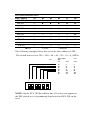
1
PCL-740
Serial Communication
RS-232/422/485/Current-Loop
Interface Card
Copyright Notice
This documentation and the software included with this product are
copyrighted 2001 by Advantech Co., Ltd. All rights are reserved.
Advantech Co., Ltd. reserves the right to make improvements to the
products described in this manual at any time without notice.
No part of this manual or software may be reproduced, copied,
translated or transmitted, in any form or by any means without the
prior written permission of Advantech Co., Ltd. Information provided in this manual is intended to be accurate and reliable. However,
Advantech Co., Ltd. assumes no responsibility for its use, nor for any
infringements of rights of third parties which may result from its use.
Acknowledgments
PC-LabCard is a trademark of Advantech Co., Ltd. IBM, PC and
PC/XT/AT are trademarks of International Business Machines
Corporation. MS-DOS, MASM, QuickBASIC, Microsoft C and MSPASCAL are trademarks of Microsoft Corporation. Intel is a trademark of Intel Corporation. Turbo C and Turbo PASCAL are trademarks of Borland International.
Part No. 200074010 2nd Edition
Printed in Taiwan May 2001
Contents
Chapter 1
Introduction .................................................. 1
Description ............................................................................. 2
Features ..........................................................................................3
Applications ...................................................................................3
Specifications .................................................................................4
Chapter 2
Hardware Installation ................................... 7
Initial Inspection ................................................................... 8
PCL-740 Jumper and Switch Locations ............................. 9
Card Configuration ............................................................ 10
Jumper settings ................................................................... 12
Card installation ................................................................. 16
Appendix A
Register structure and format ............... 17
Register Structure ............................................................... 18
Programming example ....................................................... 21
Appendix B
PC I/O Address Reference ........................ 25
PC I/O Address Usage ......................................................... 26
CHAPTER
Introduction
1
Chapter 1 Introduction
1
Description
The PCL-740 card enables RS-232, RS-422, RS-485 or current-loop
serial communication for applications in difficult environments. You
can configure its port to RS-232, RS-422, RS-485 or current-loop
using on-board jumpers.
The card features a 16C550 UARTs (with on-chip 16-byte FIFO)
making serial I/O more reliable. By buffering data into 16-byte
packets before putting it on the bus the UART drastically reduces the
CPU load. This makes the PCL-740 especially suitable for high
speed serial I/O applications and applications under MS Windows.
In RS-485 mode, the PCL-740 automatically senses the direction of
incomming data and switches its transmission direction accordingly.
Therefore no handshaking signal (e.g. RTS signal) is necessary. This
feature lets you simply and quickly build an RS-485 network with
just two wires. More importantly, application software previously
written for half duplex RS-232 environments, can be used without
modification.
2
PCL-740
User's Manual
Features
• Serial Port can be configured to RS-232/422/485 or current-loop
• 16C550 FIFO UART (with 16-byte FIFO)
• Baud rate up to 115 Kbps
• IRQ selection: 3, 4, 5, 6, 7, 9, 10, 11, 12 or 15
• Complete RS-232 modem-control signals
• Space reserved for optional surge protection (RS-422/485 only)
• Space reserved for termination resistor (RS-422/485 only)
• LED indicator on each port indicates data flow
• Automatic data-flow control in RS-485 mode
Applications
• PLC monitoring and control
• Serial communication in harsh environments
• Data entry terminals
• Remote data acquisition and control
• Instrument controller, distributed control systems
• Interface to modem, bar code reader, scale, plotter
• Multidrop communication networks
Chapter 1 Introduction
3
Specifications
Board
• Number of ports: 1
• Protocol selection: RS-232/422/485 or current-loop
• UART: 16C550 (16-byte FIFO)
• I/O address selection: From 200H to 3F8H
• IRQ selection: 3, 4, 5, 6, 7, 9, 10, 11, 12 or 15
• Power consumption: +5 V, 250 mA typical, 350 mA Max.
• Connectors: DB-9 male, DB-25 male
• Operating temperature: 32 to 122oF (0 to 50oC)
• Dimensions: 7.25" x 4.13" (18.4-cm x 10.5-cm)
• Weight: 0.2 Kg
RS-232 interface
• Signal driver/receiver: SN 75188, SN 75189
• Signals: TxD, RxD, RTS, CTS, DTR, DSR, DCD, RI, GND
• Mode: Asynchronous, full duplex
• Baud-rate: 50 to 115200 bps
• Stop bits: 1, 1.5, 2
• Parity: Even, odd or none
• Data bits: 5, 6, 7, 8
4
PCL-740
User's Manual
Current-loop interface
• Signal driver/Receiver: 6N136
• Signals: TxD+, TxD-, RxD+, RxD• Current value: 20 mA (Standard)
• Mode: Asynchronous, full duplex
• Baud-rate: 50 to 115200 bps
• Transmission distance: 1000 m
RS-422 Interface
• Signal driver/receiver: SN75176, SN75173
• Signals:
TxD+, TxD-, RxD+, RxD-, RTS+, RTS-, CTS+, CTS-, GND
• Mode: Asynchronous full duplex, point-to-point
• Max data rate: 115 Kbps
• Max data distances: 4000 feet (1220 meters)
RS-485 Interface
• Signal driver/receiver: SN75176
• Signals: DATA+, DATA-, GND
• Mode: Half duplex, multi-drop
• Max data rate: 115 Kbps
• Max data distances: 4000 feet (1220 meters)
Chapter 1 Introduction
5
6
PCL-740
User's Manual
CHAPTER
Hardware
Installation
2
Chapter 2 Hardware Installation
7
Initial Inspection
Depending on the option you ordered, you should find (in addition to
this manual) the following items inside the shipping container:
• PCL-740 1-port RS-232/422/485 or Current-loop Interface card
We carefully inspected the PCL-740 mechanically and electrically
before we shipped it. It should be free of marks and scratches and in
perfect working order on receipt.
As you unpack the PCL-740, check it for signs of shipping damage
(damaged box, scratches, dents, etc.). If it is damaged or it fails to
meet specifications, notify our service department or your local sales
representative immediately. Also notify the carrier. Retain the
shipping carton and packing material for inspection by the carrier.
After inspection we will make arrangements to repair or replace the
unit.
When you handle the PCL-740, remove it from its protective packaging by grasping the rear metal panel. Keep the anti-vibration packing. Whenever you remove the card from the PC, store it in this
package for protection.
Warning
8
Discharge your body’s stafic electric charge by
touching the back of the grounded chassis of the
system unit (metal) before handling the board. You
should avoid contact with materials that hold a static
charge such as plastic, vinyl and styrofoam. Handle
the board only by its edges to avoid static damage
to its integrated circuits. Avoid touching the exposed
circuit connectors.
PCL-740 User's Manual
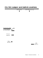
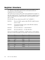
PCL-740 Jumper and Switch Locations
RS-422/485
RS-232/Current-loop
Current-loop select
Tx Active/Passive
Rx Active/Passive
Protocol
Selection
Base
Address
IRQ
Selection
Chapter 2 Hardware Installation
9
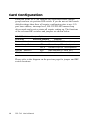
Card Configuration
Each port of the PCL-740 card has two associated status jumper
groups and one six position DIP switch. If you do not use the boards
default settings then these all require configuring prior to use. I/O
port base address, interrupt level, RS-232/422/485/current-loop
driver mode and receiver status all require setting up. The functions
of the relevant DIP switches and jumpers are shown below.
PCL-740 Switch and Jumper Options
Selection
Switches/Jumpers
Function
Protocol Selection
JP5
RS-232/422/485/Current-Loop
Current-Loop Status
JP2
Current-Loop TX active/passive
JP3,4
Current-Loop RX active/passive
Address Selection
SW1
Base address for serial port
IRQ Selection
JP1
Interrupt level for serial port
Please refer to the diagram on the previous page for jumper and DIP
switch locations.
10
PCL-740 User's Manual
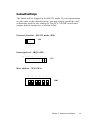
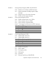
Default Settings
The board will be shipped in the RS-232 mode. If your requirements
are the same as this default setting, you may simply install the card
without the need for any setting up. The PCL-740 DIP switch and
jumper default settings are as shown below:
Protocol selection - RS-232 mode (JP5)
¡
¡
¡
¡
¡
¡
¡
¡
RS-232
RS-422
RS-485
C.L.
JP5
Interrupt level - IRQ4 (JP1)
IRQ
15 12 11 10
9
7
5
4
¡
¡
¡
¡
¡
¡
6
¡
¡
¡
3
¡
¡
¡
¡
¡
¡
¡
¡
¡
¡
¡
JP1
ON
SW1
A8
A7
A6
A5
A4
A3
Base address - 3F8 (SW1)
SW1
Chapter 2 Hardware Installation
11
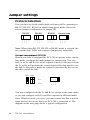
Jumper settings
Protocol Selection
First you have to decide which mode each port will be operating in,
RS-232, RS-422, RS-485 or current-loop driver mode. Select the
correct jumper configuration on jumper JP5.
RS-232
RS-422
RS-485
Current-Loop
¡
¡
¡
¡
¡
¡
¡
¡
¡
¡
¡
¡
¡
¡
¡
¡
¡
RS-232
C.L.
¡
RS-485
¡
RS-422
¡
RS-232
¡
C.L.
¡
RS-485
¡
RS-422
¡
RS-232
¡
C.L.
¡
RS-485
¡
RS-422
¡
C.L.
¡
RS-485
¡
RS-422
¡
RS-232
¡
Note: When either RS-232, RS-422 or RS-485 mode is selected, the
two current-loop Tx/Rx active/passive jumpers are inoperable.
Current-Loop jumpers (JP2,3,4)
Should you want to configure the PCL-740 to operate in the currentloop mode, configure the main jumper for current-loop. You also
have to set Tx and Rx for active or passive mode. In the active mode
the Tx or Rx will generate the current required for data transfer over
the link. In the passive mode the current is generated by the card at
the other end of the link.
TxD
RxD
¡
¡
¡
Active
Passive
¡
¡
¡
¡
¡
¡
¡
¡
C.L.
¡
RS-485
¡
¡
RS-422
¡
RS-232
¡
¡
You may configure both the Tx and Rx to operate in the same mode,
or you can configure each Tx and Rx to operate in different modes.
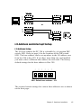
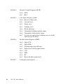
Note: Whatever mode you select you must ensure that this is not the
same mode as the device that your PCL-740 is connected to. The
diagram on the next page shows a typical configuration.
12
PCL-740 User's Manual
PCL-740
port 1
Active
Passive
Tx
Rx
Active
Passive
Rx
Tx
Desktop computer
or
Workstation
port 1
Active
Tx
Passive
Rx
Passive
Rx
Active
Tx
Plotter
I/O Address and Interrupt Setup
I/O Address Setup
A8
A7
A6
A5
A4
A3
The I/O base address the PC-740 is selectable by a 6 position DIP
switch, SW1. Refer to page 9 for the locations of the DIP switch
SW1. The base address can be set anywhere in the I/O address area
from hex 200 to hex 3F8. If you have more than one card installed
you must select a different base address for each card. The factory
default settings for the base address is Hex 3F8.
ON
SW1: Default base address - 3F8
The required switch settings for various base addresses are as shown
on the next page:
Chapter 2 Hardware Installation
13
Port base address (SW1)
Base address
200-207
208-20F
A3
l
A4
l
A5
l
A6
l
A7
l
A8
l
¡
l
l
l
l
l
¡
l
¡
¡
¡
l
¡
¡
¡
¡
¡
l
¡
l
¡
¡
¡
¡
¡
¡
¡
¡
¡
¡
- 2E8-2EF
- 2F8-2EF
- 3E8-3EF
- *3F8-3FF
l:ON
¡:OFF
*:Default
The following example shows how to set the base address to 2F8:
The switch sum is set to 2F8 = 200 + 80 + 40 + 20 + 10 + 8, (HEX).
Base address
HEX
line
value
value
A3
A4
A5
A6
A7
A8
A9
8
10
20
40
80
100
200
8
16
32
64
128
256
512
Deci-
A8
A7
A6
A5
A4
A3
mal
ON
NOTE: On the PCL-740 the address line A9 is does not appear on
the DIP switch as it is permanently hard-wired to HEX 200 on the
card.
Interrupt Level (IRQ) Setting
The PCL-740 card is designed to access interrupt levels 3 up to level
15 with the exception of 8, 13, and 14. If the card is to be designated
as COM1:, the interrupt level must be set to IRQ4 (the default). For
COM2: the setting is IRQ3. Ensure that this does not conflict with
any other card's IRQ. Simply place the jumper link on the required
interrupt level as shown below:
IRQ
15 12 11 10
9
7
6
5
4
¡
¡
¡
¡
¡
¡
¡
¡
¡
3
¡
¡
¡
¡
¡
¡
¡
¡
¡
¡
¡
JP1
Card installation
Warning! Turn off your PC’s power supply whenever you
install or remove the PCL-740 or its cables. Static
electricity can easily damage computer equipment.
Ground yourself by touching the chassis of the
computer (metal) before you touch any boards.
1. Turn off the computer. Turn the power off to any peripheral
devices (such as printers and monitors).
2. Disconnect the power cord and any other cables from the back of
the computer. Turn the PC if necessary to gain access to the
cables.
3. Remove the PC’s cover (refer to your user’s guide if necessary).
4. Locate the expansion slots or passive backplane (at the rear of the
PC) and choose any unused slot.
5. Remove the screw that secures the expansion slot cover to the PC
(save the screw to secure the interface card retaining bracket).
Remove the anti-vibration card clamp if supplied.
6. Carefully grasp the upper edge of the PCL-740 card. Align the
hole in the retaining bracket with the hole on top of the expansion
slot. Align the gold striped edge connector with the expansion
slot socket. Press the board firmly into the socket.
7. Replace the screw in the expansion slot retaining bracket.
Replace anti-vibration card holder.
8. Attach the DB-9 cable to the connector on the bracket.
9. Replace the PC’s cover. Connect the cables you removed in step
2. Turn the computer power on.
The board is now installed in the computer.
16
PCL-740 User's Manual
APPENDIX
A
Register structure
and format
Appendix A Register structure and format
17
Register Structure
This appendix gives short description of each of the module's registers. For more information please refer to the data book for the
STARTECH 16C550 UART chip.
All registers are one byte. Bit 0 is the least significant bit, and bit 7 is
the most significant bit. The address of each register is specified as an
offset from the port base address (BASE), selected with DIP switch
SW1 or SW2.
DLAB is the "Divisor Latch Access Bit", bit 7 of BASE+3.
BASE+0
Receiver buffer register when DLAB=0 and the operation is a read.
BASE+0
Transmitter holding register when DLAB=0 and the
operation is a write.
BASE+0
Divisor latch bits 0 - 7 when DLAB=1.
BASE+1
Divisor latch bits 8 - 15 when DLAB=1.
The two bytes BASE+0 and BASE+1 together form a 16-bit number,
the divisor, which determines the baud rate. Set the divisor as follows:
18
Baud rate
50
Divisor
2304
Baud rate
2400
Divisor
48
75
1536
3600
32
110
1047
4800
24
133.5
857
7200
16
150
768
9600
12
300
384
19200
6
600
192
38400
3
1200
96
56000
2
1800
64
115200
1
2000
58
PCL-740 User's Manual
BASE+1
BASE+2
Interrupt Status Register (ISR) when DLAB=0
bit 0
Enable received-data-available interrupt
bit 1
Enable transmitter-holding-register-empty
interrupt
bit 2
Enable receiver-line-status interrupt
bit 3
Enable modem-status interrupt
FIFO Control Register (FCR)
bit 0
Enable transmit and receive FIFOs
bit 1
Clear contents of receive FIFO
bit 2
Clear contents of transmit FIFO
bits 6-7 Set trigger level for receiver FIFO interrupt.
BASE+3
Bit 7
0
Bit 6
0
FIFO trigger level
01
0
1
04
1
0
08
1
1
14
Line Control Register (LCR)
bit 0
Word length select bit 0
bit 1
Word length select bit 1
Bit 1
0
Bit 0
0
Word length (bits)
5
0
1
6
1
0
7
1
1
8
bit 2
Number of stop bits
bit 3
Parity enable
bit 4
Even parity select
bit 5
Stick parity
bit 6
Set break
bit 7
Divisor Latch Access Bit (DLAB)
Appendix A Register structure and format
19
BASE+4
BASE+5
BASE+6
BASE+7
20
Modem Control Register (MCR)
bit 0
DTR
bit 1
RTS
Line Status Register (LSR)
bit 0
Receiver data ready
bit 1
Overrun error
bit 2
Parity error
bit 3
Framing error
bit 4
Break interrupt
bit 5
Transmitter holding register empty
bit 6
Transmitter shift register empty
bit 7
At least one parity error, framing error or break
indication in the FIFO
Modem Status Register (MSR)
bit 0
Delta CTS
bit 1
Delta DSR
bit 2
Trailing edge ring indicator
bit 3
Delta received line signal detect
bit 4
CTS
bit 5
DSR
bit 6
RI
bit 7
Received line signal detect
Temporary data register
PCL-740 User's Manual
Programming example
The following C example shows how to program the PCL-740's
registers directly. It uses I/O ports hex 3F8 and 2F8 to test the PCL740’s send, receive and FIFO functions.
/**************************************************/
/* Program: DEMO01.C
*/
/* Description:
*/
/*
Sends a string from COM1 to COM2 then reads */
/*
it back from COM2 and displays it on the
*/
/*
screen. It uses direct register control.
*/
/**************************************************/
#include
#include
#include
#include
<dos.h>
<io.h>
<stdio.h>
<conio.h>
/* Timeout value in seconds */
#define TIME_OUT
10000
static
static
int base0=0x3f8; /* Port 1 base address (COM1) */
int base1=0x2f8; /* Port 2 base address (COM2) */
static
static
char rec[16]; /* Receive buffer */
char cmd[16]; /* Command buffer */
void main()
{
int i;
timeout; /* counter for timeout */
char flag;
/* Set up Port 1 (COM1) */
outport((base0+2),0xc9);
/* Enable FIFO */
outp(base0+3,0x80);
/* Set DLAB=1 */
/* Set bps = 115200 */
outp(base0 ,0x01); outp(base0+1,0x00);
outp(base0+3,0x03); /* set data=8; stop=1; no parity*/
outp(base0+1,0x00); /* disable interrupt */
Appendix A Register structure and format
21
/* Set up Port 2 (COM2) */
outport((base1+2),0xc9);
/* Enable FIFO */
outp(base1+3,0x80);
/* Set DLAB=1 */
/* Set bps = 115,200 */
outp(base1 ,0x01); outp(base1+1,0);
outp(base1+3,0x03); /* Set data=8; stop=1; no parity*/
outp(base1+1,0x00); /* Disable interrupt */
printf("\nEnter string (max 15 char) or Q to quit:");
gets(cmd);
while (cmd[0] != ‘q’ && cmd[0] != ‘Q’)
{
/* Send string on Port 1 (COM1) */
i=0;
cmd[strlen(cmd)] = 0x0d;
flag=1;
while (flag)
{
outportb(base0,cmd[i]); /* Send data */
if (cmd[i] == 0x0d)
flag=0;
i++;
}
22
PCL-740 User's Manual
/* Receive data on Port 2 (COM2) */
i=0;
flag=1;
timeout=TIME_OUT;
while (flag)
{
/* Check for received data on port*/
if ((inportb(base1+5) & 1) !=0)
{
rec[i]=inportb(base1); /* Receive data */
if (rec[i] == 0x0d)
{
rec[i+1]=’\0';
flag=0;
printf(“\nReceived data: %s\n”, rec);
}
i++;
}
else
{ /* Check timeout */
timeout—;
if (timeout == 0)
{
flag = 0;
printf(“\nTimeout error\n”);
}
}
} /* End of receive data while() */
printf("\nEnter string (max 15 char) or Q to quit:");
gets(cmd);
} /* End of "Enter string" while() */
} /* End of main() */
Appendix A Register structure and format
23
24
PCL-740 User's Manual
APPENDIX
PC I/O Address
Reference
B
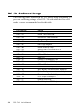
Appendix B: PC I/O Address Assignments
25
PC I/O Address Usage
The following table indicates the PC I/O address usage assignment. To
prevent conflicting settings of the PCL-740 with other devices or I/O
cards, you are recommended to refer this table.
26
I/O Address
Device
000 - 00F
DMA (8237A)
020 - 021
8259A IRQ Controller
040 - 043
8253/8254 Timer/Counter
060 - 063
PPI 8255A
070 - 071
Real-Time Clock
080 - 08F
DMA Page Register
0A0 - 0BF
8259A Interrupt Chip
0C0 - 0DF
Second DMA Controller 8237A
0F0 - 0FF
Math Coprocessor
1F0 - 1F8
AT Fixed Disk
200 - 20F
Game I/O
278 - 27F
Parallel Printer Adaptor #2
2F8 - 2FF
Serial Adaptor ( COM 2 )
320 - 32F
XT Fixed Disk
378 - 37F
Parallel Printer Adaptor #1
380 - 38F
SDLC Binary Communication Adaptor
3A0 - 3AF
Master Binary Communication Adaptor
3B0 - 3BF
Monochrome/Parallel Adaptor
3D0 - 3DF
Color Graphics Adaptor
3F0 - 3F7
Diskette Controller
3F8 - 3FF
Serial Adaptor ( COM 1 )
PCL-740 User's Manual