1
Designing Standard Cells ASICs with the ASIC
Design Kit (ADK) and Mentor Graphics Tools
Version 3.1
The purpose of this document is to provide university students with the basic flow and procedures for using Mentor Graphic’
design tools with ADK design kit. The usage of this document is intended for student use only and in no way should be perceived
as a complete process guide. Please refer to standard Mentor Graphics documents for complete process information.
NOTE: This document covers the Standard Cell ASIC flow only. For information of the custom IC (Schematic Driven Layout:
SDL) flow, please refer to the ADK SDL App Note at: http://www.mentor.com/company/higher_ed .
Copyright 1996-2005
Table of Contents
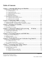
Chapter 1 - Simulating HDL Designs in ModelSim..........................................5
1.1. Simulating your RTL Design ..........................................................................................5
1.1.1. Invoking ModelSim .....................................................................................................................5
1.1.2. Compiling HDL code...................................................................................................................6
1.1.3. Setting up the ModelSim windows ..............................................................................................7
1.1.4. Applying stimulus........................................................................................................................7
1.1.5. Running the Simulator ...............................................................................................................10
1.2. Simulating Gate-level netlists .......................................................................................10
1.2.1. Compile the ADK Simulation Libraries ....................................................................................10
1.2.2. Compile the Gate-level design...................................................................................................11
1.2.3. Simulate the Gate-level Netlist ..................................................................................................11
Chapter 2 - Synthesizing VHDL or Verilog.....................................................12
2.1. Synthesizing HDL Using Leonardo (GUI Mode).........................................................12
2.2. Synthesizing HDL Using Spectrum (Command-Line Mode) ......................................14
Chapter 3 - Designing for Testability...............................................................15
3.1. Inserting Scan chains.....................................................................................................15
3.2. Generating Test Vectors................................................................................................16
Chapter 4 - Automated Standard Cell Layout using
IC Station ..............18
4.1. Generating Schematics and Viewpoints........................................................................18
4.2. Autoplacement and Routing..........................................................................................18
4.3. Verifying Project Layout...............................................................................................21
Chapter 5 - Generating Padframes and GDSII Data .....................................24
5.1. Top Level Layout Preparation.......................................................................................24
5.2. Padframe Layout ...........................................................................................................25
5.3. Preparing Fabrication Data............................................................................................26
Chapter 6 - Performing Post-Layout Verification Using Mach-TA ..............27
6.1. Preparing to Simulate the Design..................................................................................27
6.1.1. Creating Test Vectors ................................................................................................................27
6.1.2. Creating a Command File ..........................................................................................................27
6.2. Running Test Vectors and Viewing Results .................................................................28
Chapter 7 - Performing Static Timing Analysis..............................................29
7.1. Setting Up and Invoking SST Velocity.........................................................................29
7.2. Setting Timing Constraints............................................................................................29
7.2.1. Defining Clocks .........................................................................................................................30
7.2.2. Defining Constraints on Input Pins ............................................................................................30
7.2.3. Defining Constraints on Output Pins .........................................................................................30
Page 3 of 36
Designing ASICs with Mentor Graphics
Copyright © 1999 – 2005 Mentor Graphics
Rev. 9/15/2005 2:38 PM
7.2.4. Defining False Paths.................................................................................................................. 30
7.2.5. Defining Constant Levels .......................................................................................................... 30
7.2.6. Back Annotating from a SDF File............................................................................................. 31
7.3. Timing Analysis ........................................................................................................... 31
Appendix 8 - ADK Menus and Commands .................................................... 32
8.1. ADK_DAIC.................................................................................................................. 32
8.1.1. Schematic Edit menu................................................................................................................. 32
8.1.2. ADK IC Library menu .............................................................................................................. 33
8.1.3. Cell Library menu ..................................................................................................................... 33
8.2. ADK_IC........................................................................................................................ 34
8.2.1. ADK pulldown menu ................................................................................................................ 34
8.2.2. ADK Edit palette menu ............................................................................................................. 34
8.2.3. ADK Commands ....................................................................................................................... 36
Page 4 of 36
Designing ASICs with Mentor Graphics Tools
Copyright © 1999 – 2005 Mentor Graphics
Rev.9/15/2005 2:38 PM
Chapter 1 - Simulating HDL Designs in ModelSim
You can invoke the ModelSim simulator on any compiled VHDL or Verilog design. Once you invoke
ModelSim, you can apply stimulus to the design, run the simulation, analyze the results, and modify the
design based on those results. You can then reset the simulator, optionally revise or apply more stimulus to
the design, and start the cycle over. When the design functions correctly, you can save the stimulus and
simulation results directly with the design.
The typical strategy for simulation is an iterative process that will be utilized during two steps of the overall
design process:
Verify functionality of HDL code prior to synthesis
Verify functionality once the design is placed and routed.
Although the focus of each phase is different, the tasks that you perform within the simulator are very
similar.
The following procedure describes how to simulate an HDL design:
1.1. Simulating your RTL Design
After you create your HDL design, you can simulate it in ModelSim to verify that the design works as
expected. The following sections outline this process:
1
Invoking ModelSim
2
Compiling HDL code
3
Setting up the ModelSim windows
4
Applying stimulus
5
Running the Simulator
1.1.1. Invoking ModelSim
You can invoke ModelSim by double-clicking on the ModelSim icon or entering the following line on the
shellcommand line:
% vsim model
If you specify a design name (model), ModelSim will attempt to load the last compiled architecture or
interface of the specified model from the work library.
If you did not specific a design name on the invocation line, then ModelSim will display a dialog box that
allows you to verify the library name (in most cases it will be work) and select the design that you want to
simulate.
Page 5 of 36
Designing ASICs with Mentor Graphics
Copyright © 1999 – 2005 Mentor Graphics
Rev. 9/15/2005 2:38 PM
1.1.2. Compiling HDL code
1.
Change to the directory containing your HDL source code. For example:
cd $DESIGNS/src
2.
If you have not already done so, map the Logical HDL library to a physical directory (File > New >
Library... ):
vlib
vmap
vlib
vmap
phy_lib_path
logical_lib phy_lib_path
$DESIGNS/hdl/work
work $DESIGNS/hdl/work
In this example. all files compiled into the “work” library would be saved in the $DESIGNS/hdl/work
directory. This information is saved in the modelsim.ini file.
3.
Run the HDL compiler from the GUI or using the following tool/shell commands (Compile >
Compile...):
vcom filename.vhd (for VHDL)
vlog filename.v (for Verilog)
To compile a VHDL file into a predefined library:
vcom [-work logical_lib] VHDL_source
vcom -work work $DESIGNS/src/count4.vhd
and for Verilog you would use
vlog [-work logical_lib] Verilog_source
vlog -work work $DESIGNS/src/count4.v
If you do not specify the “-work logical_lib” information, then the compliers will compile the HDL code
into the work library.
This is simply a compilation step. You can invoke the HDL simulator (vsim) on the compiled object in the
work library. The simulator is the only tool that uses this compiled object, the synthesis tool reads the HDL
code into memory without saving the compiled object to disk.
NOTE: If you get an error about can’t find “work” library or running vlib, then execute the following two
commands in a UNIX shell:
vlib /my_path/designs/work
vmap work /my_path/designs/work
o Fix any errors and explain all warnings
o Determine the Next Step
After your HDL code compiles correctly you can either simulate the compiled object in ModelSim or
synthesize the HDL using Leonardo.
Page 6 of 36
Designing ASICs with Mentor Graphics Tools
Copyright © 1999 – 2005 Mentor Graphics
Rev.9/15/2005 2:38 PM
1.1.3. Setting up the ModelSim windows
ModelSim has a set of windows that allows you to view your design and simulation results. In most cases,
you will only be using the Main, Source, and Wave windows.
1.
Display the source HDL code (View > Source)
VSIM > view source
2.
•
Displaying signal waveforms
To add all top-level signals:
VSIM > add wave /*
•
To add a specific signal:
VSIM > add wave signal_nameVSIM > add wave clockVSIM > add wave curr_state
•
To re-order the list of signals, Select and hold down the LMB on the signal in the wave window (it
will be highlighted with a box) and then move the mouse until the skinny green box is at the point
where you want to move the signal.
NOTE: You can also define the order that signals are added by using explicitly wave commands when you
set up the Wave window. For example:
add
add
add
add
•
wave
wave
wave
wave
clock
clear
enable
count
To remove a signal, select the signal in the wave window (it will be highlighted with a box) and
select the Edit > Cut menu item in the Wave Window
1.1.4. Applying stimulus
ModelSim and HDLs provide several methods for providing stimulus (vectors) for your design. Typically,
you will use a ModelSim force file to interactively generate test vectors and then move to a HDL testbench
after the basic functionality of the design has been created.
1.1.4.1. Using Force Files (interactive)
A signal changes value either by the user applying stimulus to the signal (force command) or by the
simulator applying stimulus due to design functionality. The following list shows examples of how to apply
forces to the design. Typically, you only apply forces to signals defined in the top-level entity:
•
To apply stimulus to a signal:
force signal_name value time
If you do not specify a time, then ModelSim applies the force at the current simulation time. Some
examples:
force reset 1
force reset 0 100
Page 7 of 36
Designing ASICs with Mentor Graphics
Copyright © 1999 – 2005 Mentor Graphics
Rev. 9/15/2005 2:38 PM
• To specify a clock signal
force clock time_value_pair, time_value_pair -repeat period
There must be an even number of time_value_pair combinations. For example:
force clk 0 0, 1 25 -repeat 50 # 50nS clock with 50% duty
force clk 0 5, 1 15 -repeat 50 # 50 nS clock with 10nS low
pulse
1.1.4.2. Force File Example 1
## initialize design
force clear 1 0
force enable 1 0
force clock 0 0, 1 25 -repeat 50
## apply stimulus
force clear 0 10
force enable 0 430
force enable 1 530
1.1.4.3. Force File Example 2 (loops)
## initialize design inputs
set time 0
force clock 0 0, 1 25 -repeat 50
force reset 1 0
force enter_sensor 0 0
force exit_sensor 0 0
force reset 0 30
## Use TCL commands to count up to 15
for {set num 0} {$num <= 15} {incr num 1} {
incr time 50
force enter_sensor 1 $time
incr time 50
force enter_sensor 0 $time
incr time 100
force exit_sensor 1 $time
incr time 50
force exit_sensor 0 $time
incr time 50
}
incr time 200
force exit_sensor 1 $time
incr time 50
force exit_sensor 0 $time
incr time 100
force exit_sensor 1 $time
Page 8 of 36
Designing ASICs with Mentor Graphics Tools
Copyright © 1999 – 2005 Mentor Graphics
Rev.9/15/2005 2:38 PM
incr time 50
force exit_sensor 0 $time
1.1.4.4. VHDL Test Bench example
LIBRARY ieee;
USE ieee.std_logic_1164.all;
ENTITY bcd_tb IS
END bcd_tb;
ARCHITECTURE test OF bcd_tb IS
COMPONENT bcd -pre-compiled Device to Test
PORT (rst, clk, enable, load, up_down : IN std_logic;
data : IN std_logic_vector(3 downto 0);
bcd_out : OUT std_logic_vector(6 downto 0) );
END COMPONENT;
SIGNAL rst, clk, enable, load, up_down : std_logic;
SIGNAL data : std_logic_vector(3 downto 0);
SIGNAL bcd_out : std_logic_vector(6 downto 0);
BEGIN
u1 : bcd PORT MAP (clk => clk,
rst => rst,
load => load,
enable => enable,
up_down => up_down,
data => data,
bcd_out => bcd_out);
-- Initialize all input signals
clk <= ‘0’;
rst <= ‘1’;
load <= ‘0’;
enable <= ‘1’;
up_down <= ‘1’;
data <= “0101”;
-- Specify 10 ns clock
clock: process (clk)
begin
clk <= NOT (clk) after 5 ns;
end process;
-- Specify Test Vectors
stim: process ()
begin
rst <= ‘0’ after 15 ns;
enable <= ‘0’ after 63 ns;
enable <= ‘1’ after 87 ns;
load <= ‘1’ after 163 ns;
load <= ‘0’ after 187 ns;
Page 9 of 36
Designing ASICs with Mentor Graphics
Copyright © 1999 – 2005 Mentor Graphics
Rev. 9/15/2005 2:38 PM
up_down <= ‘0’ after 203 ns;
end process;
END test;
1.1.5. Running the Simulator
To run the simulator for a specified amount of time, use the following command:
VSIM > run time
For example, to run the simulator for 1000 ns, enter:
VSIM > run 1000
If you just type “run” then the simulator runs for 100 nS.
1.2. Simulating Gate-level netlists
After you synthesize, insert scan chains or layout the design, you may want to simulate the gate-level
design. At these points, you can also apply a SDF file to the design to get actual gate delay values. The
following sections outline this process:
1. Compile the ADK Simulation Libraries
2. Compile the Gate-level design
3. Simulate the Gate-level Netlist
1.2.1. Compile the ADK Simulation Libraries
If you want to compile a gate-level netlist (typically produced by Leonardo) that contains ADK cells, you
will need to compile the VITAL (VHDL) or Verilog cell models into a ModelSim library (similar to how
you compile your design into the “work” library).
1. Create a “ADK” work library
vlib /user/student/designs/adk
2. Map the Logical name to the physical directory created in the previous step
vmap adk /user/student/designs/adk
3. Compile the ADK VITAL(VHDL) or Verilog into the ADK “work” library. For VITAL models:
vcom $ADK/technology/adk.vhd -work adk
vcom $ADK/technology/adk_comp.vhd -work adk
For Verilog models:
vlog $ADK/technology/adk.v -work adk
Since more than one person will be simulating gate-level netlists using the ADK, you may want to select one
location on the network to place the compiled ADK library. To access the library, you would only need to
map the logical “adk” name to the physical location using vmap.
Page 10 of 36
Designing ASICs with Mentor Graphics Tools
Copyright © 1999 – 2005 Mentor Graphics
Rev.9/15/2005 2:38 PM
1.2.2. Compile the Gate-level design
Just like your RTL design, you must compile your gate-level design prior to simulation. For VHDL designs,
you must have the following LIBRARY and USE statements to specify the VHDL component declarations:
LIBRARY adk;
USE adk.adk_components.all;
To compile the HDL gate-level netlist, you can either run the compiler from the command line or within the
ModelSim GUI.
1.2.3. Simulate the Gate-level Netlist
After the design and libraries have been compiled, you can simulate the design. Typically, you will simulate
the design to verify it is still functionally correct. Once this is verified, you can simulate the design with
annotated timing numbers (from a SDF file produced by Leonardo or post-layout).
To simulate the design, follow these steps:
1
2
3
Display the Simulation Dialog Box (Simulate > Simulate...)
Select the design unit to simulate in the Design tab
Optionally, specify the SDF file to apply in the SDF tab
The SDF file can be applied to different levels of hierarchy (regions) of the design. If you get a lot of error
messages about “unable to find instance” during SDF annotation, then you probably applied the SDF file at
the wrong level of hierarchy. For example:
o If you are using a Force file as stimulus, then you usually want to apply the SDF file to the toplevel (/) of the simulated design.
vsim -sdfmax /=/user/ericc/cs/osu/mult.sdf work.mult
o If you are using a HDL testbench as stimulus, then you usually want to apply the SDF file to the
Design-Under-Test (DUT) block.
vsim -sdfmax /dut=/user/ericc/cs/osu/mult.sdf work.mult
4.
Begin the simulation by clicking the OK button
Page 11 of 36
Designing ASICs with Mentor Graphics
Copyright © 1999 – 2005 Mentor Graphics
Rev. 9/15/2005 2:38 PM
Chapter 2 - Synthesizing VHDL or Verilog
The following section describes how to synthesize the HDL code that you created, compiled and simulated
in the earlier chapters. As usual, this chapter provides an overview of the flow and does not go into all the
options available.
2.1. Synthesizing HDL Using Leonardo (GUI Mode)
You can invoke Leonardo by double-clicking on the Leonardo Spectrum icon or entering the following
command on the shell command line:
Leonardo
The following list describes the basics of optimizing a design for the ADK using the Leonardo synthesis
tool:
Step 1: Load the technology library (Technology FlowTab)
In this step, you will load the cell definitions for the specific technology. The ADK includes about 90 cells
characterized with timing, capacitance, function, and area information.
1. Select the desired ADK library from the ASIC -> ADK library list in the Technology FlowTab.
If the ADK libraries do not appear in the GUI, you can manually load them by entering the following
command on the tool command line:
load_lib $ADK/technology/leonardo/<lib_name>
The available technologies are ami12_[worst|typ|fast], ami05_[worst|typ|fast],tsmc035_[worst|typ|fast],
and tsmc025_typ.
2. Ignore the process variables (in the Technology FlowTab)
Although the Technology FlowTab displays the PVT derating factors, they have no affect on the
timing values in the library.
FYI: The slow process corner uses a temperature of 80 degrees C, a voltage of 4.5 volts, and a process
number of 3 sigmas. The fast process corner uses a temperature of 0 degrees C, a voltage of 5.5 volts,
and a process number of -3 sigmas. The typical process corner uses a temperature of 27 degrees C, a
voltage of 5.0 volts and a process number of 0 sigmas.
3. Load the library by clicking on the Load Library button
Step 2: Read the VHDL file(s) (Input FlowTab)
After you load the library, you can read your HDL files into Leonardo. The synthesis tool does not use any
of the information compiled into ModelSim; you must read all HDL source into Leonardo.
1. Select the Input Flowtab
2. Set the working directory
Page 12 of 36
Designing ASICs with Mentor Graphics Tools
Copyright © 1999 – 2005 Mentor Graphics
Rev.9/15/2005 2:38 PM
3. Add the HDL files to the open files list.
4. Click on the Read button to synthesize your design to generic gates.
You should observe the resultant transcript for the following warnings/messages:
o Warning about unexpected latches
o Verify number of operators (e.g. adders) is as expected
o Verify number of sequential elements is as expected
Step 3: Optimize the design to the target technology (Optimize FlowTab)
After you read the HDL files, you can map the design to a specify technology using the optimize command.
In this step, Leonardo will map the registers to technology cells, implement operators into optimal
configurations, and minimize the remaining boolean logic.
The Optimize FlowTab allows you to specify the following options:
1. Target Technology: Choose the desired technology from the picklist.
2. Hierarchy: Choose preserve to keep the design hierarchy in the synthesized design (aids in
debugging), or flatten to merge the design into a single level of hierarchy (allows optimization across
hierarchical boundaries).
3. Add I/O Ports: MAKE SURE THIS OPTION IS NOT SELECTED. The current release of the ADK
library for Leonardo does NOT include support for automatic IO insertion. You will need to
manually add IO using Design Architect.
4. Run timing optimization: This option forces Leonardo to make an additional opti-mization pass to
help critical paths meet timing specifications. Leonardo optimizes the original result of synthesis
(reading in the design) so running multiple optimization passes will not produce significantly better
results. The first optimization iteration is usually as good as it gets.
Step 4: Determine the Size and Speed of the optimized design
After the design is mapped to a technology, you can generate reports to determine whether your
design meets the size and timing constraints.
1. Determine the gate count (Report FlowTab: Report Area PowerTab)
2. You should examine the area report to examine the size of your design and that Leonardo used the
correct number of memory resources (flip-flops).
3. Set timing constraints (Constraints Flowtab : Clock PowerTab)
4. At a minimum, you should specify the clock periods for all clocks in your design. Most critical paths
will occur on register-to-register timing paths. You may also want to set arrival constraints on any
unregistered input signals, plus “required” times on any unregistered output signal.
5. Determine the critical path (Report FlowTab: Report Delay PowerTab)
Page 13 of 36
Designing ASICs with Mentor Graphics
Copyright © 1999 – 2005 Mentor Graphics
Rev. 9/15/2005 2:38 PM
Step 5: Save the Design (Output FlowTab)
Specify a filename (usually the name of the top level entity). You should also save this netlist file in a
separate directory. (e.g. $DESIGNS/netlist). You should set the following variables in Leonardo (prior to
writing out the VHDL netlist) to add the required VHDL component declarations:
set vhdl_write_use_packages {library ieee,adk; use
ieee.std_logic_1164.all; use adk.adk_components.all;}
You will usually save two netlists:
o Verilog netlist for IC Layout
o VHDL or Verilog Netlist for simulation in ModelSim.
2.2. Synthesizing HDL Using Spectrum (Command-Line Mode)
If you prefer to write scripts or just want a way to automate your synthesis runs, you don’t have to use the
Lenardo GUI. All you need is a script and then the command
spectrum -file script.name
will run the synthesis using your script. Here is an example of a script that will read in several VHDL files
and synthesize to the ADK:
## ADKsynthesis script
Step 1: Load the library
load_library tsmc035_typ
# Step 2: Read the HDL files
read { abmux.vhd alu.vhd control.vhd datamux.vhd top.vhd }
#Step 3: optimize the design to a technology
optimize
#Step 4: Optionally set timing constraints
and generate reports
set_attribute -net clk -name clock_cycle -value 10
optimize_timing
report_delay
report_area -cell
#Step 5: Write out the netlist
set vhdl_write_use_packages {library ieee,adk; use
ieee.std_logic_1164.all; use adk.adk_components.all;}
apply_rename_rules -ruleset VHDL
apply_rename_rules -ruleset VERILOG
auto_write netlist/top.gate.sdf
auto_write netlist/top.gate.vhd
auto_write netlist/top.gate.v
Page 14 of 36
Designing ASICs with Mentor Graphics Tools
Copyright © 1999 – 2005 Mentor Graphics
Rev.9/15/2005 2:38 PM
Chapter 3 - Designing for Testability
The following sections describe how to use DFTAdvisor and FastScan with the Mentor Graphics’ ADK to
insert scan and generate test vectors.
3.1. Inserting Scan chains
This process has been largely automated by the DFTAdvisor tool. The following steps will get you started
using a default configuration and you can then experiment with the options as you gain more familiarity with
the tools.
Step 1: (For VHDL netlists) Create dft.map file in your working direc-tory:
Using your favorite editor, map the VHDL packages used in your design to the VHDL source files. The
sysnthesis and DFT tools do not use the compiled ModelSim HDL code, they must read the HDL source
into memory. You can inform DFTAdvisor of the VHDL packages by creating a file called dft.map and
enter these lines:
standard $MODEL_HOME/vhdl_src/std/standard.vhd
std_logic_1164 $MODEL_HOME/vhdl_src/ieee/stdlogic.vhd
adk $ADK/technology/adk.vhd
adk_components $ADK/technology/adk_comp.vhd
Step 2: Invoke dfta:
Run DFTAdvisor on your structural HDL netlist for your design. The first example if for VHDL, the second
for Verilog.
dftadvisor -vhdl design.vhd -lib $ADK/technology/adk.atpg \-log dfta.log -replace
[-nogui]
dftadvisor -verilog design.v -lib $ADK/technology/adk.atpg \-log dfta.log replace [-nogui]
Step 3: Inset Scan chain:
You can use the GUI or simply enter these commands in the command window. This is a simple
configuration, but will demonstrate the basic steps necessary to insert a scan chain.
set system mode setup
analyze control signal -auto
set system mode dft
run
insert test logic -num 1
report scan chains
Step 4: Write the scan netlist:
You need to write out the new netlist with your scan chain instantiated. Again, simply type these commands
in the command window.
Page 15 of 36
Designing ASICs with Mentor Graphics
Copyright © 1999 – 2005 Mentor Graphics
Rev. 9/15/2005 2:38 PM
write atpg setup design.scan -replace
write netlist design.scan.vhd -replace
Step 5: Exit DFTAdvisor
exit -discard
3.2. Generating Test Vectors
Once you have inserted your scan chains, you need to generate the test vectors that will be used to test your
circuit. You use FastScan to do this. Here is a general procedure for taking your scan design written from
DFTAdvisor and generating your test vectors:
Step 1: Invoke FastScan in GUI mode:
You can simply type
fastscan
to bring up a dialog box that will prompt you for all the proper arguments.
Step 2: Fill out the dialog box:
For Design, enter the name of the scan design you output from DFTAdvisor.
Be sure the Format is correct for HDL source.
Enter the correct top-level name for Top Module.
Enter $ADK/technology/adk.atpg for ATPG Library. NOTE: You must substitute your full path for $ADK
in the GUI. It will not expand your environment variable.
Enter a name for the output log file, if desired. Click on the Invoke FastScan
button to run FastScan.
Optionally, you can do all this from the command line:
fastscan -vhdl design.vhd -lib $ADK/technology/adk.atpg -top
design -dofile ./design.scan -log fastscan.log
Step 3: Generate test patterns:
At this point, you should be ready to generate patterns. Your dofile that was generated from DFTAdvisor
that you ran in FastScan set up your circuit’s scan and clocks. All you need to do is enter the following
commands:
set system mode atpg
add fault -all
run
save patterns top.pat
exit -discard
Optionally, you can use the GUI or create a dofile with these commands in it and run that with
dofile dofile.name
At this point, you have an HDL netlist with scan chains and a pattern file with the test patterns used to test
your circuit.
Page 16 of 36
Designing ASICs with Mentor Graphics Tools
Copyright © 1999 – 2005 Mentor Graphics
Rev.9/15/2005 2:38 PM
This is only a very basic introduction to using the DFT tools. See the Mentor documentation for more
features and on how to debug your circuit should you have any problems with these tools on your netlist.
Page 17 of 36
Designing ASICs with Mentor Graphics
Copyright © 1999 – 2005 Mentor Graphics
Rev. 9/15/2005 2:38 PM
Chapter 4 - Automated Standard Cell Layout using
IC Station
You will now be guided step-by-step through IC layout . You will use automatic place and route tools to
establish the internal layout. You will also learn how to perform LVS and DRC checks.
4.1. Generating Schematics and Viewpoints
Once you have synthesized and created your Verilog netlist, you need to generate an EDDM database and
schematic to drive the IC layout tools. You do this with DA-IC’s import Verilog feature. Launch DA-IC
using adk_daic then choose File -> Import Verilog. Use the following settings:
o Netlist File(s) : netlist/design.gate.v
o Output Direcotry: project directory (e.g. $PROJECT or $MGC_WD)
o Mapping File(s) : $ADK/technology/adk.vmp
where design is the name of your design (top, above). You can also click the Netlist File(s).. button and
browse to find the desired settings. You now have an EDDM schematic which can be used with IC Station
or Eldo. It is generally best to create a symbol of your design before proceeding to ensure the ports are
netlisted properly.
To do this choose Miscellaneous -> Generate Symbol. The default settings should be sufficient so simply
click OK. Once the symbol is done click the Check & Save button to complete the symbol.
Once you have created a symbol you will want to create a netlist of your design for use with Calibre. This is
done by clicking Update LVS in the schematic_edit palette.
Before the actual layout process begins, the design needs to be prepared for use with the layout tools. The
viewpoints are created for the ICBlocks tools, specifcally. This process is automated by calling the script
adk_dve from your design-project directory.
For ADK parts: run $ADK/bin/adk_dve <design> -t <tech>. This will create several viewpoints of your
design. The one we will be using for automated place and route is the layout viewpoint.
4.2. Autoplacement and Routing
Autoplacement and routing is the process of automatically generating a layout from a previously existing
schematic or design. To increase our confidence in the correctness of a generated result, we setup ICgraph
(the layout editor) to carefully check every action taken by ICblocks (the autoplacement/router). We will
now describe ICblocks use to automatically place and route a layout. These steps will walk you through a
relatively simple, direct path to an automatically placed and routed layout. Generally, it is best to create a
new directory to hold your layouts. IC Stations file browser filters out EDDM files and directories, so don’t
put your layouts inside your EDDM component directory.
Page 18 of 36
Designing ASICs with Mentor Graphics Tools
Copyright © 1999 – 2005 Mentor Graphics
Rev.9/15/2005 2:38 PM
Step 1: Invoke IC Station
The ICgraph tool is the main entry point into the IC Station environment. Before running the tool, however,
we need to set the $MGC_WD environment variable to the directory where the design resides. This can be
performed with the Unix alias-macro "swd". To invoke IC Station from the unix command prompt, simply
type "adk_ic". This is a special version of IC Station that has been enhanced with special features for the
ADK.
Step 2: Create an IC cell
Select "CREATE" from the menu on the right hand side of the screen. A form titled "CREATE CELL" will
appear. Enter the following,then click OK:
Cell Name : $PROJECT/[layout_dir]/[design_name]
Attach Library : $ADK/technology/ic/process/[library]
Process: $ADK/technology/ic/process/[process_file]
Rules File: $ADK/technology/ic/process/[process.rules]
Angle Mode : 45
Logic Source : $PROJECT/[design_name]/layout
Logic Source Type : EDDM
Logic Loading: Flat
$PROJECT is your path to the directory where you created your schematic. Table 1 shows the valid options
for the other fields. All other options should be left at default values. It is very important to change the
logic loading to flat if you have any logic other than standard cells in your design. It is always safe to
load flat so it is recommended to do so, always.
Once you click OK on this dialog box a cell window will appear having the name of the design.
Note: Currently there is an issue with the load_logic function used by create. If you get an error you will
need to manually open the logic source. This can be done in the ADK Edit palette using Logic -> Open.
Table 1: Variable Fields for Cell Creataion
Variable Name
Possible Values
Description
library
ami05
ami12
tsmc035
tsmc025
ami05
ami12
ami15
tsmc035
tsmc025
tsmc018
ami05.rules
ami12.rules
ami15.rules
tsmc035.rules
These are the libraries of standard cells and pads.
Currently, only pads are available for tsmc035.
The library for ami15 and ami12 are both ami12.
No characterization has yet been done for ami15
These are the process files for the currently
available processes.
process_filel
process.rules
The standard rules files are for all flows except
Accusim backannotation. If you want to extract
for backannotation to Accusim, use the
*.accusim.rules file.
Page 19 of 36
Designing ASICs with Mentor Graphics
Copyright © 1999 – 2005 Mentor Graphics
Rev. 9/15/2005 2:38 PM
tsmc025.rules
tsmc018.rules
Step 3: AutoFloorplan the IC cell
Select Place & Route from the IC Palette (or P&R from the ADK Edit Palette) then choose autofloorplan
(Autofp) in the Place & Route Palette. Allow all options to default simply by clicking on OK in response to
the Autofloorplan Options form. Use View -> All from the top menu bar to see the automatically generated
floor plan. You will see a series of boxes enclosed by solid bars along each edge. The boxes indicate the
rows into which cells will be organized. The solid bars indicate edges of the cells along which physical
ports will be placed.
Step 4: AutoPlace the standard cells
Choose Autoplace Std Cells (StdCel under Autoplc) in the Place & Route palette, and click on OK in the
form, once again leaving all options to their default values. You should see individual cells placed in the
floorplan boxes. Cell locations are determined by their interconnectivity. Cells which share connections are
placed near one another. You may wish to experiment with the results obtained thus far by selecting
different Autofloorplan and Autoplace options.
Step 5: AutoPlace Ports
Select Autoplace Ports (Ports under Autoplc) in the Place & Route palette. You can allow the options to
default for now, but you may wish to experiment with them later also. You will see lightly shaded areas
along the port bars at the edge of the layout.
At this point, it is assumed that you have arrived at a satisfactory initial placement for all cells of the layout.
Prior to autorouting the interconnect, you may wish to observe a "rats nest" view of the signals connecting
the various cells. This is sometimes useful to the layout technician for determining sources of routing
congestion. To observe a rats nest of signal connections, select Connectivity -> Net -> Restructure -> All
signal from the top menu bar. It may look a little messy, but keep in mind that it doesn't change the layout
whatsoever.
Step 6: AutoRoute the IC cell (Autoroute All from the Place & Route palette)
From the palette menu select "All" from the "Autorou" subsection of the menu. A submenu will appear in
the editing window . Select "Options" and "Expert" options and select "Channel Over Cell Routing". From
the "OCR" options menu set the step size to .5 and the "Operation Mode Type" to "Center Weighted". OK
all the forms and begin routing. Depending on the size of the design this may take several minutes. When
the process has completed the mouse pointer changes back from an hourglass to an arrow and the results of
the process are in the transcript. Several small overflows may still exist, which can be expected for larger
designs. These overflows are addressed in the next step.
NOTE: There is a know issue with ICBlocks (DR00265739) that will sometimes create shorted nets when
using OCR. These shorts can be avoided by using the default options for autoroute_all. This will impact the
final area some but should create a layout free of short circuits. It is also possible to hand edit the final
layout to fix the shorts if better area results are required.
Page 20 of 36
Designing ASICs with Mentor Graphics Tools
Copyright © 1999 – 2005 Mentor Graphics
Rev.9/15/2005 2:38 PM
To fix the shorts by hand, perform the following steps:
o Click Checking -> Shorts - all nets, then click ok. This will identify all the shorts in your design.
o Click Checking -> First Error to highlight the first short.
o Select the overlapping paths/vias and delete them. Each short generally consists of several
overlapping paths/vias and the highlighting will only be for one of these at a time. Make sure to
delete them all before proceeding.
o Auto-route the resulting overlfow(s) (see below).
o Click Checking -> Next Error until a new short is highlighted then repeat steps 3 to 5 until no more
shorts exist.
Step 7: Find Overflows and Route Them
This step is necessary even if overflows don’t immediately appear in the routed layout. When zoomed out
small overflows may not be viewable, but may still exist. To select all overflows in the design type "check
over". In the form window that appears select "All"and OK the form. Next, from the Place and Route
palette menu select "Overflw". If the response "An object of type Overflow must be selected" appears in the
status block, there are no overflows to route. Otherwise, the overflows should be routed.
Step 8: Add Text to the Ports
Before the layout is complete we need to add text to the ports and prepare the design for use with Calibre.
This can be done by clicking the Port Text button in the Add subsection of the ADK Edit palette.
NOTE: The port text is used by Calibre to identify the ports in your design. Without the text, the extracted
netlist would be virtually useless.
Step 9: Save the IC cell
Save the layout by selecting File -> Cell -> Save Cell -> Current Context. You may save the layout and exit
the ICgraph session at any time. To re-load the layout later, choose open from the IC staton palette. If you
wish to make changes to the cell, you must also select File -> Cell -> Reserve Cell -> Current Context.
4.3. Verifying Project Layout
For layout verification, the physical layout data is interpreted in at least two important ways.
o The first determines if the geometries within the layout meet a set of physical design rules established by
the IC foundry. This helps insure a more manufacturable and reliable chip.
o The second determines whether the layout precisely conforms to the schematic developed during the
front end design phase. This of course helps guarantee that the actual fabricated circuit will perform as
much like the front end simulation as possible.
Although the automatic tools performed the layout in Correct by Construction mode, it is always good to
verify the layout for correctness in terms of both layout design rules and connectivity to insure consistency
between the varous tools used. This establishes a system of "checks and balances" that increases the overall
confidence in the design. First check for layout design rule errors using ICrules, then verify the layout by
double checking it against the transistor level representation of the logic diagram.
Page 21 of 36
Designing ASICs with Mentor Graphics
Copyright © 1999 – 2005 Mentor Graphics
Rev. 9/15/2005 2:38 PM
NOTE: When you check the entire layout you will find some DRC errors in the pad frame as well as any
DRC errors that still exist in the cell layout. The pad frame errors are inconsequential and are a result of
using an optional set of design rules. Focus on the design rules that exist independent of the pad frame by
excluding certain cells from the DRC.
o Select Check from the ICrules palette.
o Click on options in the resulting prompt bar, and enter the following under exclude cell: PadOut
PadSpace PadBidir PadInC PadGnd PadVcc PadFC (and any other pad names you see in your
padframe). If you also did a DRC on your core logic, you can even exclude it from the checks.
This will exclude all pad cells from the DRC check, and any errors will be exclusively related to your cell
and the top level interconnect.
Step 1: Check Layout Design Rules
From the main ICstation palette select ICrules, then select Check from the ICrules palette. A prompt box
will appear at the lower left of the screen. Click on OK to proceed with the check. Optionally, if you are
using the ADK Edit menu, you can use Drc->Check.
Step 2: Step 2: Fix any Design Rule Errors
When the check is complete, design rule errors which exist in the layout will be reported in the message bar
at the bottom of the ICstation window. The first one can be shown by selecting "First" in the palette (or
DRC->First in the ADK Edit palette). Then rest can be viewed by clicking on "Next". As an example, one
or more design rule errors of the type "DRC4_4_p_space: P+ select space = 2L" may exist. The design rule
checker is complaining about p-select mask layers being too close in adjacent cells. A similar error may
occur with n-select masks.
Step 3: Verify connectivity between schematic and layout
Verify the layout for consistency with the transistor level schematic of your design. This is done using
Calibre LVS.
o From the menu bar select Calibre -> Run LVS. This will launch Calibre Interactive - LVS.
o In the pop up window enter $ADK/technology/calibre/lvs.<tech>.runset, where <tech> is the ADK
technology used for this design. Then click OK. This sets up Calibre to perform an LVS check for
the desired technology.
o Calibre Interactives GUI has 3 main parts a menu bar at the top, a button palette on the left and
display area. The display area will change based on the current selection in the button palette. You
should notice some of the buttons will be highlighted red, this indicates settings which have not been
set correctly. Begin by clicking the Inputs button on the left.
o The Layout and H-Cells tabs should be set correctly. The Netlist tab tells Calibre where to get the
source netlist for comparison. Click ... and browse to find the source netlist. If you followed the
instructions above, It should be located in your logic source directory as a file named
<design>.src.net.
o You should now be all set to perform an LVS check so click Run LVS. If a pop up asks to
overwrite the layout file click OK to ensure Calibre sees any recent changes to your layout.
Page 22 of 36
Designing ASICs with Mentor Graphics Tools
Copyright © 1999 – 2005 Mentor Graphics
Rev.9/15/2005 2:38 PM
o When Calibre has completed the LVS check you should see two new windows. One has the text
LVS Report File and the other is Calibre - LVS RVE. If you passed the LVS check the Report file
should contain a check mark and a smiley face. Calibre - LVS RVE allows you to browse through
any errors which have been found and highlight them in IC Station. If you do highlight any errors be
sure to click the eraser button in the icon palette at the top to remove the highlighting before you quit
RVE. Otherwise the highlights will stay until you launch RVE again and erase them.
Step 4: Save the IC layout
Save your completed project layout by selecting File -> Cell -> Save Cell -> Current Context.
4.4. Post-Layout Extraction using Calibre PEX
With the layout complete and passing LVS and DRC, it is time to extract the layout parasitic netlist. This
will give you a spice netlist of your layout complete with resistance, parasitic capacitance and coupling
capacitance. For the extraction process you will use Calibre Interactive - PEX.
o In IC Stations menu bar, select Calibre -> Run PEX. This will launch Calibre Interactive - PEX.
o In the pop up window enter $ADK/technology/calibre/lvs.<tech>.runset, where <tech> is the ADK
technology used for this design. Then click OK. This sets up Calibre to perform an extraction for
the desired technology.
o Begin by clicking the Inputs button. The Layout and H-Cells tabs should again be set correctly.
To use the same port/net names for your extracted netlist that were used in your logic source you will
need to point Calibre to your source netlist. This is done in the Netlist tab. Click … and browse to
find the source netlist. It should be located in your logic source directory as a file named
<design>.src.net.
o Now select the Outputs button. At the top, the Extraction Type should be Transistor Level and you
can choose one of the following types:
RCC - Distributed RC network with coupling capacitors
RC - Distributed RC network without coupling capacitors
C - Lumped net capacitance with coupling capacitors
You should now be all set to perform the extraction so click Run PEX. If a pop up asks to overwrite the
layout file click OK to ensure Calibre sees any recent changes to your layout.
When Calibre has completed the extraction a window will pop up showing the top level of the extracted
netlist. Notice that there may be up to two additional netlists which will be included into the top level. The
first will contain the RC networks and the second will contain the coupling capacitors.
NOTE: You should not attempt to extract your design once it has been put into a padframe.
Page 23 of 36
Designing ASICs with Mentor Graphics
Copyright © 1999 – 2005 Mentor Graphics
Rev. 9/15/2005 2:38 PM
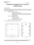
Chapter 5 - Generating Padframes and GDSII Data
The ADK has a facility for automatically generating a TinyChip padframe for fabrication through MOSIS.
If you wish to automatically generate and route to your padframe, you need to prepare your design data in a
particular manner to facilitate this feature.
5.1. Top Level Layout Preparation
To begin, you need a top level part containing the design inside a padframe. Start by creating a top level
schematic for the whole chip that includes both the pads and the design core. The core logic needs to have a
symbol for each piece and a property called phy_comp for ‘‘physical component’’ and no comp property.
Simply place your core logic and the pads which will drive the automatic padframe generator in IC Station.
Step 1: Create a symbol for your core logic:
In Design Architect you need to generate a symbol (Miscellaneous -> Generate Symbol) for each piece of
core logic that you want to instantiate in the pad frame. You will have to have a completed IC layout for
each component for which you have a symbol at this top level. These can be SDL or standard cell designs
or a combination of both.
Once you have generated your symbol, you need to add the phy_comp property-string to the symbol body.
The value of phy_comp needs to be the name of the IC cell that you created (or will create). Do not place a
comp property on this symbol.
Step 2: Use Choose Symbol to bring in the design part(s)
and wire them together if necessary. Perform a check -> sheet and just ignore the unconnected pin
warnings. You can also eliminate the reporting of these warnings by selecting check -> sheet -> set defaults
and setting dangles to errors only.
Step 3: In the ADK Library menu choose the pads to use
from the appropriate library for your technology. Based on the technology, there may be different types of
pads available. You can only use one set of technology pads and it must agree with the technology of your
design.
Add the pads to your schematic and wire them up to your core logic. Change the property PINXX
(shift+F7) to replace the XX with the pin number on the package you wish to connect this signal to in the
final design. Be sure to add power/VDD/GND pads as necessary. Any pads not in your schematic will not
appear in your completed padframe. Check and save your schematic.
NOTE: For all processes, the corner pads will be automatically instantiated for you. For ami12, this
includes the power corner pads which power the padframe. Y ou still must instantiate core-logic power and
ground, however.
Page 24 of 36
Designing ASICs with Mentor Graphics Tools
Copyright © 1999 – 2005 Mentor Graphics
Rev.9/15/2005 2:38 PM
Step 4: Use adk_dve to create proper viewpoints for the top-level design.
Run adk_dve [design] like you did for other schematics. This will create the necessary viewpoints for layout
and verification.
5.2. Padframe Layout
In IC station (adk_ic) you can create a new cell for the top-level logic and the padframe that will be
generated based on your schematic.
NOTE: The automatic padframe generator will only generate 40-pin tiny-chip padframes at this time.
1. Create a new layout cell for the whole chip. Enter the following in the new cell form, allowing all
else to default:
Cell Name: $PROJECT/layout/[design_name]
Attach Library: $ADK/technology/ic/[process_cell_lib]
Process: $ADK/technology/ic/[process_file]
Rules File: $ADK/technology/ic/[process.rules]
Angle Mode: 45
Logic Source: $PROJECT/layout
Logic Source Type: EDDM
Logic Loading: Flat
2. Go to the ADK Edit palette menu and click on Open to open the logic source window. You should
see your schematic in a new window.
3. Select the core logic (if you have more than one piece, select them all). Then click on Inst on the
DLA Logic palette to place these cells into your layout window. Remember, you must have
previously designed these cells and they must have the name of the phy_comp property on your
symbol.
4. If you wish to store your completed cells in a location other than your current working directory, you
will need to set your search path from the IC Station Setup->SDL menu. The search path should
look something like this:
$ADK/technology/ic/ami05_via $PROJECT/cells.
5. The last ‘‘.’’ is important for it includes the current, or working directory. Simply add any other
paths you wish to search for your cells.
6. Once you have placed the core logic block(s), you are ready to generate your padframe. Do not
place the pads, yourself. Use the ADK->Generate Padframe->AMI 0.5 (or the appropriate
technology for your design) pulldown menu to generate the padframe.
7. Make life easy on yourself. NEVER EDIT OR RELOCATE PAD CELLS.
8. View the entire cell, now, to see the padframe and your logic (Shift-F8). You should see the entire
padframe with corner pads, the pads you asked for and spacer pads for all the empty spaces (or
analog pads for the case of the ami12 technology). You will also see overflows showing which ports
get wired to which pins.
9. At this point you might notice that your core logic should be rotated, flipped or moved to make
routing easier. Do that, now, but be careful not to move the pads.
10. After finalizing the placement of your core logic, you can route the pads to the core. You can do this
Page 25 of 36
Designing ASICs with Mentor Graphics
Copyright © 1999 – 2005 Mentor Graphics
Rev. 9/15/2005 2:38 PM
manually or automatically.
11. To autoroute, click on P&R on the ADK Edit palette menu to bring up the Place & Route palette
menu. Then click on All under Autorou. On the prompt-bar that appears click Options and unselect
Expand Channels from the menu. Click OK on the menu and prompt-bar to autoroute the pads
12. Now take a look at the final layout and fix any problems. For example, you might not like the width
or placement of the power busses. You can edit these routes (or opt to manually route them,
initially) until you are satisfied with the final result.
5.3. Preparing Fabrication Data
Once your layout is complete and you are ready to send your design for MOSIS for fabrication, you will
need to perform the following steps:
Step 1: Create a new top-level cell for your scaled design:
Create a new cell in GE (geometry editing) mode. Make sure you specify the correct process for the cell.
Step 2: Add your completed cell to this new cell:
Use Add->Cell to add your top-level design to this new cell. This top-level should include your wired
padframe as well. You should not do any editing of your cell that this point.
Step 3: Scale your cell to the correct technology:
Use the ADK->Scale menu to select the technology you are targeting. This will appropriately scale your
design for that technology.
Step 4: Write out GDSII for your cell:
o Use Translate->ICLink to write a GDSII stream (or CIF but MOSIS prefers GDSII and it will scale
properly with no manual edits). Select the source format as ICgraph and the destination as GDSII.
Click OK and another dialog box will appear that will ask for the source and destination names and
option file.
o Enter the name of your source cell (or use the navigator), the destination (including any extension
such as .gdsii) and the option file. For the option file, you should use ADK/lib/iclink_gdsii.options.
A GDSII file will be produced and this is what you will send to MOSIS. Be sure to check MOSIS s web
pages for proper submission procedures and technology codes. For all processes, the ADK uses the submicron (SUBM) design rules so you should specify that in your technology code. If you used the second
poly layer, be sure to use the code for that as well. If you do not use the second poly layers then you can use
either the single or dual poly technology codes. You will simply get a warning about no data on the second
poly layer if you have none. This can be safely ignored.
Page 26 of 36
Designing ASICs with Mentor Graphics Tools
Copyright © 1999 – 2005 Mentor Graphics
Rev.9/15/2005 2:38 PM
Chapter 6 - Performing Post-Layout Verification
Using Mach-TA
Mach TA is an analog simulation tool for performing timing analysis and functional verification of digital
designs. Its role in the ADK-kit design flow is to perform analysis on netlists extracted from a design layout
in IC station.
6.1. Preparing to Simulate the Design
Mach TA uses SPICE netlists as its input. To get a SPICE netlist for your design, do an IC Extract(M)>Lumped from the IC Palettes menu in IC Station (or click on Extract in the ADK Edit palette menu). In
the form that appears select the Netlist button, enter the filnename for the netlist, and enter the ground-node
name as ‘GND’. OK the form to generate the netlist.
An incongruence exists between the format of the netlist that IC Station provides and the format expected by
Mach TA. Specifically, the netlist generated by IC Station is defined as a subcircuit while Mach TA expects
a flat file with no defined subcircuits. To correct this an awk script $ADK/bin/mta_prep.awk has been
provided in the kit to reformat the netlist. To use the script invoke:
cat [design].sp | nawk -f $ADK/bin/mta_prep.awk | sed
’s/\+/\*\+/g’ >![design].mta.sp
The second pipe though sed may not be necessary as that it only removes ‘+’ line wrapping in netlist files
with an excessive number of ports defined in the subcircuit.
6.1.1. Creating Test Vectors
To apply stimulus to a design-netlist Mach TA requires a test vector (.tv) file in Lsim format. This can be
acquired from early Modelsim test results be either using the VTRAN conversion utility
(www.sourceiii.com) or writing a customized script to convert the simulation results.
6.1.2. Creating a Command File
A command dofile for Mach TA makes it very convenient to automate test-vector analysis. Such a dofile is
automatically generated when using the mta_layout_prep script for test vector creation. An example script
would look like:
.dc
plot v(clear) v(clock) v(enable) v(output(0)) v(output(1))
v(output(2)) v(output(3))
run -tvend -dc count4.tv
Page 27 of 36
Designing ASICs with Mentor Graphics
Copyright © 1999 – 2005 Mentor Graphics
Rev. 9/15/2005 2:38 PM
This script performs initial DC analysis, selects which port pins signals to plot, and starts test vector analysis
with test-vectors in a file called count4.tv
6.2. Running Test Vectors and Viewing Results
Step 1: Invoking Mach TA
To invoke Mach TA on a netlist using the nominal ami05 technology corner case
mta -t $ADK/technology/mta/ami05 -tc NOM [design].mta.sp
This brings up the application and loads the design. To execute a pre-created dofile type ‘dof
[design_dofile_name].do’at the command-line to begin analysis. Commands can also be typed in manually
on the command line in the lower command window. See the previous section on dofiles for example
commands.
Step 2: Viewing Results
Once test-vector analysis has passed (and hopefully completed) the simulation waveforms selected by the
‘plot(node_name)’ command can be viewed from Tools->Wave Viewer drop-down menu. If the display
doesn’t initially look correct select the equal button on the top row of the window to view the entire
simulation period.
Given the case where the test vectors were derived from the ModelSim simulation results, the simulation
output from both tools should be comparable.
Page 28 of 36
Designing ASICs with Mentor Graphics Tools
Copyright © 1999 – 2005 Mentor Graphics
Rev.9/15/2005 2:38 PM
Chapter 7 - Performing Static Timing Analysis
One of the most critical aspects of VLSI design is timing analysis. The ADK includes the necessary library
files to use the SST Velocity static timing analysis tool to perform slack analysis, find longest or shortest
delay paths, or examine clock statistics. The ADK also supports post-layout back annotation of designs for
static timing analysis.
7.1. Setting Up and Invoking SST Velocity
Before working with a VHDL design, you must define a velocity.map file in your local directory that will
map the logical names of design units and standard packages to their physical locations. The velocity.map
file must include the locations of all design subunit files which are referenced in the top level file. For a
description of creating a velocity.map file and examples, refer to the VHDL section of the “Setting Up a
Design” chapter in the SST Velocity User’s Manual.
After creating the velocity.map file (VHDL users only), you must then set the target technology. In the pulldown menu ‘File’, choose the ‘Set Technology’ option. Choose your desired technology from the list of
available libraries.
When you have chosen a target technology, you will now be able to choose File>Open>Design. Navigate to
your top level design and click on the ‘OK’ button.
7.2. Setting Timing Constraints
SST Velocity requires that you set the following constraints before executing timing analysis. Setting
constraints is the most important part of timing analysis. If you set the constraints too aggressively, SST
Velocity will report inaccurate timing violations. If you set constraints that are too relaxed, the resultant
design might not meet the timing requirements of the system outside the design being analyzed. A more indepth discussion of timing parameters can be found in the “Specifying Timing Parameters” and
“Backannotating a Design” chapters of the SST Velocity User’s Manual.
Using the ‘Specify’ Menu - For a given level of the design hierarchy, the ‘Specify’ menu enables you to
specify various timing constraints for either ports or nets. The design must be fully constrained before
meaningful results can be obtained. To determine whether or not you have specified all timing constraints,
click on the pull-down menu choice Report>Missing Timing Specifications>All.
Page 29 of 36
Designing ASICs with Mentor Graphics
Copyright © 1999 – 2005 Mentor Graphics
Rev. 9/15/2005 2:38 PM
7.2.1. Defining Clocks
Clocks define the timing between registers. Without clocks defined, all registers are assumed unconstrained
and all combinational logic between registers will be ignored during timing analysis. When you define a
clock, you have effectively constrained the maximum delay between all registers to one clock period.
You can describe clocks in SST Velocity using the Specify>Clock Definitions pull-down menu. When
defining a clock, be sure to specify the clock period, duty cycle (edge positions), arrival time variance (edge
region), and slew.
Setting a Single Clock - If your design only has one clock, you define the clock using the commands in the
previous example. Your design will have only one clock domain.
Setting Multiple Synchronous Clocks - If you have multiple clocks in your design that are not in isolated
clock domains (a register in one domain drives logic connected to a register in another domain), then you
may define multiple clock signals within the same clock domain.
7.2.2. Defining Constraints on Input Pins
The input arrival time attribute specifies the maximum delay from outside the present design to the input
port and the minimum and maximum slew that signal may exhibit. You can specify input arrival constraints
at any input ports in your design, at any level of the hierarchy. All input arrival times start at time zero and
cannot be specified relative to a particular clock edge. Arrival times are specified by choosing ‘Input Arrival
Times...’ from the ‘Specify’ pull-down menu.
7.2.3. Defining Constraints on Output Pins
The output required time specifies the maximum time allowed from the register (or primary input) to the
output port. The time value is always relative to time zero and cannot be specified relative to a particular
clock edge. You can specify output constraints at any output ports in your design, at any level of the
hierarchy. Required times are specified by choosing ‘Output Setup/Hold Times...’ from the ‘Specify’ pulldown menu.
7.2.4. Defining False Paths
False paths are paths in the design that you want SST Velocity to ignore during timing analysis. To
eliminate a false path from consideration during timing analysis, designate the path as a false path by
indicating the ‘from’ and ‘to’ points or “through” points on the path. These points can be listed in the ‘False
Paths...’ option in the ‘Specify’ pull-down menu.
7.2.5. Defining Constant Levels
It may be necessary in certain designs to define pins as being held at a constant logic level. Such paths may
include set, reset, or enable pins that would put the design in an undesired state for timing analysis. To
define a constant level on a pin, choose the ‘Assign Constant Level.’ option from the ‘Specify’ pull-down
menu.
Page 30 of 36
Designing ASICs with Mentor Graphics Tools
Copyright © 1999 – 2005 Mentor Graphics
Rev.9/15/2005 2:38 PM
7.2.6. Back Annotating from a SDF File
If you intend to back annotate a design from a post-layout SDF file, you must first load the file by specifying
the desired SDF file in the File>Open>Back Annotation screen. This will replace the library delay values
with those calculated based on the actual physical layout of the design.
7.3. Timing Analysis
Now that the timing constraints of your design have been described, you can perform several different types
of timing analysis.
To perform a slack analysis, you can select either the ‘Setup/Recovery Constraints’, ‘Hold/Removal
Constraints’ or ‘Clock Pulse Widths’ option from the Report>Timing Violations pull-down menu. These
options let you select a specific path by indicating To and From pins or you can analyze the entire design by
clicking on the ‘OK’ button.
To determine the longest or shortest delay paths in a design, select the ‘Longest Delay Paths’ or ‘Shortest
Delay Paths’ option from the Report>Delay Paths pull-down menu. Again you can either specify a
particular path or analyze the entire design.
Clock information such as clock tree details, gating locations, merged clock locations, clock skew statistics,
clock latency statistics, clock pulse width statistics, and asynchronous domain crossings can be determined
by selecting the desired option from the Report>Clock Information pull-down menu.
A more in-depth discussion of timing analysis can be found in the “Analyzing a Design” chapter of the SST
Velocity User’s Manual.
Page 31 of 36
Designing ASICs with Mentor Graphics
Copyright © 1999 – 2005 Mentor Graphics
Rev. 9/15/2005 2:38 PM
Appendix 8 - ADK Menus and Commands
The ADK provides some enhanced functionality over the standard Mentor tools. There are several new
menus, palettes and commands that have been created to ease the use of the tools for ADK designs. You
will only see these enhancements if you use the ADK version of the tools (such as adk_daic or adk_ic). If
you use the standard tool, it will not have any of the ADK enhancements.
8.1. ADK_DAIC
adk_daic is the command that will start Design Architect with the ADK extensions. If you use this
command, you will have the following additional functionality in Design Architect:
8.1.1. Schematic Edit menu
The basic Schematic edit palette has been altered to make it easier to work with the ADK. The first section
of the Schematic Edit menu will let you gain quick access to other palette menus and feature specific to the
ADK. These buttons are also present on several other menus in DA-IC.
o
o
o
o
o
o
o
o
o
o
o
o
o
o
o
o
o
o
o
o
o
Session: will take you to the top-level, session menu
Library: will take you to the DA-IC Libraries menu
ADK IC Library: Short cut to the ADK’s SDL Parts menu (see below)
Simulation: will switch DA-IC to simulation mode
Prep for Layout: Creates the viewpoints need for layout using IC Station. Also creates the netlist
needed by Calibre. This is intended for use with schematic driven layout (SDL) only
Update LVS: Updates or creates a netlist of your design for use with Calibre
Edit: will take you to the schematic edit menu
Draw: will take you to the DA-IC draw menu
Text: will take you the DA-IC text edit menu. The next section, labeled Select has some basic
selection functions.
By Property: Allows you to select objects based on a specified property
Unselect All: Unselect all currently selected objects. The Edit section contains basic operations
needed when editing a schematic.
Move: Move the selected object(s) to the location you specify
Copy: Copy selected object(s) to location you specify
Delete: Deletes the selected object(s)
Undo: Undo the last action
Rotate: Rotate the selected object(s)
Flip: Flip the selected object(s). The Add section contains operations that allow you to add objects to
your schematic.
Instance: this function allow you to add your own instances to a schematic
Wire: this function allows you to draw a wire on your schematic
Bus/Bundle: this function allows you to draw a bus on your schematic
Port: will place either an in, out or bi-directional port at the location you specify
Page 32 of 36
Designing ASICs with Mentor Graphics Tools
Copyright © 1999 – 2005 Mentor Graphics
Rev.9/15/2005 2:38 PM
o Add Source: adds a current or voltage source to your schematic
o Property: this function adds a property to the selected object. The Name section contains basic
naming operations.
o Instance: will name all selected instances either automatically or manually
o Net: used to name all selected nets. The final section is labeled Miscellaneous.
o Connect: will connect all unconnected pins/nets which overlap (indicated in the schematic by a small
circle with a line through it)
8.1.2. ADK IC Library menu
Under the standard DA-IC Libraries menu you will see a new item ADK IC Library. This selection will
display the ADK IC Library palette menu which will have all of the libraries specific to the ADK on it.
o Schematic: will take you to the schematic edit menu
o Standard Cells: will take you to the Cell Library menu. The rest of this menu contains schematic
models for the parts that may be used for schematic driven layout (SDL). These include fourterminal FETs for all technologies and capacitor and resistors for some technologies. In addition,
some generic parts are supplied, such as GND, VDD and ports, as well as various voltage and
current sources.
8.1.3. Cell Library menu
Here you will find all of the standard cells supplied in the ADK.
o SDL Parts: Takes you to the ADK IC Library
o Basic Logic Gates: This library contains all of the schematic models for the basic logic standard cell
gates and their variants: AND, NAND, NOR, OR, FADD, MUX. The number following the gate
name indicates the number of inputs for the AND, NAND, NOR and OR gates. The number after
FADD indicates the number of bits in the full-adder and for the MUX indicates the number of inputs
and outputs (e.g. MUX21 has two inputs and one output).
o Inverters and Buffers: This library contains all of the schematic models for the inverters and buffers.
Each in multiple drive strengths. The number following each gate is the drive strength for the gate.
These are relative numbers so an INV02 has twice the drive strength as an INV01. See the datasheets
on the cells for more specific, absolute, drive strength information.
o AO Gates: This library contains all of the schematic models for the AND-OR gates. The numbers
following the name indicate the groupings of inputs to the AND gates. An AO21 gate has a twoinput AND gate and a one-input AND gate (a wire) all feeding into a two-input OR gate. An AO221
would have two, two-input AND gates and a wire feeding into a three-input OR gate.
o AOI Gates: This library contains all of the schematic models for the AND-OR-INVERT gates. The
numbers following the name indicate the groupings of inputs to the AND gates. An AOI21 gate has a
two-input AND gate and a one-input AND gate (a wire) all feeding into a two-input NOR gate. An
AOI221 would have two, two-input AND gates and a wire feeding into a three-input NOR gate.
o OAI Gates: This library contains all of the schematic models for the OR-AND-INVERT gates. The
numbers following the name indicate the groupings of inputs to the OR gates. An OAI21 gate has a
two-input OR gate and a one-input OR gate (a wire) all feeding into a two-input NAND gate. An
OAI221 would have two, two-input OR gates and a wire feeding into a three-input NAND gate.
o Flip-Flops/Latches: This library contains all of the schematic models for the d-type flip-flops, d-type
latches and scan, d-type flip-flops. The r and s letters following the cell name indicate the presence of
any asynchronous reset and/or set inputs, respectively.
Page 33 of 36
Designing ASICs with Mentor Graphics
Copyright © 1999 – 2005 Mentor Graphics
Rev. 9/15/2005 2:38 PM
o Pads: This library contains all of the schematic models for the pads in each sup-ported technology.
This library is subdivided into a separate library for each technology. Be sure to select the
appropriate technology for the pad libraries so as to match your target technology. See the MOSIS
web page for more information on the pads: http://www.mosis.org.
8.2. ADK_IC
adk_ic is the command that will start IC Station with the ADK extensions. If you use this command, you
will have the following additional functionality in IC Station:
8.2.1. ADK pulldown menu
Once you open a cell, you will see a new, additional menu called ADK in the menu bar. This menu allows
you to do several tasks specifically related to ADK designs:
o Show ADK Palette: This will change the palette to display the ADK palette menu. This is a quick
way to display that menu no matter which palette is currently displayed.
o Scale: This will display a submenu that will allow you to scale your design based on your target
technology. You must have your cell reserved for edit and you must be in GE mode to scale. It is
recommended that you instantiate you final layout into a new GE mode cell and then scale that new
cell. In this way you can more easily retarget to a different technology should you later decide to do
so.
o Generate Padframe: This will display a submenu where you can automatically generate a padframe
for a 40-pin tinychip based on your target technology. See the chapter Automatic Padframe
Generation for more information.
8.2.2. ADK Edit palette menu
A new palette menu has been created which contains most of the commonly used operations that you will
need for doing designs with the ADK. You can show this palette by selecting ADK->Show ADK Palette
from the pulldown menu or by clicking on ADK Edit at the bottom of the session palette.
The first section of the ADK Edit menu will let you gain quick access to other palette menus.
o Top: will take you to the top-level, session menu
o Edit: will take you to the standard edit menu for more editing functions than are presented on the
ADK Edit menu
o P&R: will take you to the place and route palette menu for placement and routing
o of your standard cell designs. The next section, labeled SDL has functions to help you preform your
schematic-driven layout.
o Logic: This will display a submenu that will let you set your logic source, close the logic or update
your logic should you have made an update outside of IC Station.
o Open: opens the current logic source in a schematic window
o Place: This will display a submenu to allow you to select instances or ports, and to place unplaced
instances and ports.
o Inst: Instantiates all selected instances into your cell or all unplaced instances should you not have
any schematic instances selected.
o AutoInst: will automatically instantiate all unplaced instances into your cell.
o Port: place selected ports or all ports if none currently selected.
Page 34 of 36
Designing ASICs with Mentor Graphics Tools
Copyright © 1999 – 2005 Mentor Graphics
Rev.9/15/2005 2:38 PM
o DEdit: This will display a submenu that will give you options on editing placed devices. You will
have options to move MOS pins, split and join MOS devices, define the folding for MOS devices
and modify capacitor and resistor properties as well.
o Clean: This will clean up your schematic should a placement abort due to an error. If your schematic
updating seems to be stuck, try to clean it up. The section on routing has many useful functions for
routing your devices and cleaning up your layout.
o Route: This is a menu with options to help you create overflows and manage your routing database.
o SsNet: This function will select all nets that are shorted or of the same net to the currently selected
object.
o MkPort: This will make the selected object a port. You will be prompted for the type and name of
the port.
o SsPort: The nets connected to the selected port will be selected for you.
o ResAll: This function will restructure all nets in your design and update the overflows to display the
updated database. Useful after moving many objects or if you see stray overflows in your cell.
o ResSel: Restructure selected net(s) only.
o AutoR: Autoroute the currently selected overflow. This will only route on the metal routing layers. It
will not route on poly.
o Comp: Compact your design. This runs the IC Station compactor. The next section has functions to
add various shapes and text.
o Port Text: This function adds text to each port, which is needed by Calibre.
o Shape: This is the Add Shape command to allow you to add arbitrary shapes on any layer you wish.
o Path: This function allows you to place paths in your cell.
o AddR: Add Route. This is the routing tool to manually route your design. This will only route on the
metal routing layers defined in the process.
o Text: Allows you to add text to your cell.
o The Edit section provides several functions for editing your cell and the objects in the cell.
o Copy: Copy selected object(s) to location you specify.
o Move: Move the selected object(s) to the location you specify.
o Align: Align selected object(s).
o Rotate: Rotate the selected object(s).
o Flip: Flip the selected object(s).
o Stretch: Stretch the selected objects (cannot be used on devices).
o The verification section of the palette menu allows your to easily perform DRC/LVS and extraction
of your cell without leaving the palette.
o DRC: This menu allows you to run the DRC check and then to scan through the results and view
your DRC errors, if any.
o Load Rules: If you need to change the rules that you are using, use this option to load a new rules
file.
o Extract: This function will perform a lumped, mask-level extraction of your circuit suitable for
simulation with ELDO, Mach-TA or Accusim.
o LVS: Run a mask-level LVS of your cell.
o Report: LVS reporting functions. The options in this menu allow you to view the LVS report and to
check your LVS errors, if any. Finally, the last item is Repeat. This is a toggle switch that will turn
on or off the repeatable functions. Functions with an asterisk (*) by them will repeat. If you do not
want those functions to repeat, click on the Repeat item to turn it off, and click on it again to turn it
Page 35 of 36
Designing ASICs with Mentor Graphics
Copyright © 1999 – 2005 Mentor Graphics
Rev. 9/15/2005 2:38 PM
back on.
8.2.3. ADK Commands
In addition to the new menus, there are some new commands (or macros) that have been included with
adk_ic. Some of these commands are specific to creating and maintaining your standard cells, and are
offered as examples that you can modify for your own needs.
To use any of these commands, simply type them in the cell window. A prompt bar will appear with your
command in it.
Table H-1.
Function
Description
pc
Place a poly contact; places a poly contact centered at the
current cursor position.
pr
Places standard cell power rails; Places a VDD and a GND
power rail in metal 1 with the height of a standard cell. Also
creates proper port and net properties for the rails. These rails
are short, but can be stretched to and desired width for your
cell.
nwc
Place an n-well contact; creates and places an n-well contact
on the standard cell power rails.
pwc
Place a p-well contact; creates and places p-well contact on
the standard cell power rails.
pfp
Place an fp1 layer; For standard cells, you need to specify an
fp1 (floor plan) layer. This command automatically generates
and places one to the extent of the cell.
p
Place a poly path of width 2 (minimum width); Prompts you
to place a poly path.
m
Place a metal1 path of width 3 (minimum width); Prompts
you to place a metal1 path.
v
Move unconstrained; Moves the selected object(s).
ab1
Add metal1 blockages to entire cell; This command will
place a metal1 blockage on top of all metal1 shapes in your
cell. This is useful for autorouting with hierarchy.
rab1
Remove metal1 blockages; This command will remove all
metal1 blockages in your cell.
s25
Set cell process to TSMC 0.25
s35
Set cell process to TSMC 0.35
s12
Set cell process to AMI 1.2
Page 36 of 36
Designing ASICs with Mentor Graphics Tools
Copyright © 1999 – 2005 Mentor Graphics
Rev.9/15/2005 2:38 PM
s5
Set cell process to AMI 0.5
cp
Checkpoint cell; save the cell and then reserve the cell.
dup
Delete unplaced ports; If LVS reports unplaced ports but you
see that they are all placed from your schematic; the database
might have duplicate ports. This command will remove them.
Page 37 of 36
Designing ASICs with Mentor Graphics
Copyright © 1999 – 2005 Mentor Graphics
Rev. 9/15/2005 2:38 PM