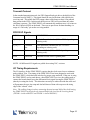
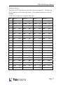
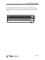
1
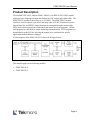
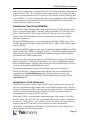
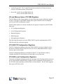
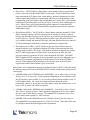
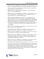
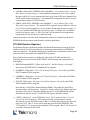
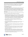
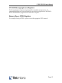
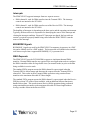
FastPMC Products
FastPMC-PEO32
32-bit PECL/ECL Output Module
User’s Manual RevB
TEK/TM-295B
March 2002
FPMC-PEO32 User’s Manual
TEK Microsystems has made every effort to ensure that this manual is accurate and complete.
However, TEK reserves the right to make changes and improvements to the products described
in this manual at any time and without notice.
This product is covered by a limited warranty which is described in the manual. Other than the
stated limited warranty, TEK disclaims all other warranties, including the warranties of
merchantability and of fitness for a particular purpose. In the event of a failure of the hardware
or software described in this manual, TEK’s obligation is limited to repair or replacement of the
defective item, or, if the item cannot be repaired or replaced, a refund of the purchase price for
the item. TEK assumes no liability arising out of the application or use of the hardware or
software, and assumes no responsibility for direct, indirect, incidental or consequential damages
of any kind.
The electronic equipment described in this manual generates, uses, and can radiate radio
frequency energy. Operation of this equipment in a residential area is likely to cause radio
interference, in which case the user, at his own expense, will be required to take whatever
measures may be required to correct the interference.
TEK Microsystems’ products are not authorized for use as critical components in life support
devices or systems without the express written agreement of an officer of TEK Microsystems.
This manual is Copyright © 2001, TEK Microsystems, Incorporated. All Rights Reserved.
FastPMC is a trademark of TEK Microsystems, Incorporated.
Other trademarks and registered trademarks used are owned by their respective manufacturers.
Revision Information:
This manual describes hardware revision “A” of the FPMC-PEO32.
Document ordering code and release information:
URL: http://www.tekmicro.com/tm295B.pdf
TEK/TM-295B
March 2002
Page 1
FPMC-PEO32 User’s Manual
Table of Contents
Product Description ......................................................................................................4
Specifications ................................................................................................................5
Support Information ......................................................................................................6
Warranty Information................................................................................................................ 6
Contact Information .................................................................................................................. 6
Additional Documentation........................................................................................................ 7
Installation and Setup ...................................................................................................8
Overview ................................................................................................................................... 8
Unpacking and Handling........................................................................................................... 8
Installation................................................................................................................................. 9
Software Download and Installation....................................................................................... 10
Theory of Operation ....................................................................................................11
Overview ................................................................................................................................. 11
PCI Interface ........................................................................................................................... 11
Local Bus ................................................................................................................................ 12
Buffer Memory........................................................................................................................ 12
Serial EEPROM ...................................................................................................................... 14
Customizable FPGA................................................................................................................ 14
Clock Architecture .................................................................................................................. 15
Transmit Protocol.................................................................................................................... 16
PEO32 I/O Signals .................................................................................................................. 16
I/O Timing Requirements........................................................................................................ 16
Software Interface .......................................................................................................19
Overview ................................................................................................................................. 19
Initialization ............................................................................................................................ 19
Initialization: Serial EEPROM Load................................................................................ 20
Initialization: PCI Address Configuration........................................................................ 22
Initialization: Read Serial EEPROM................................................................................ 23
Initialization: Clock Synthesizer ...................................................................................... 23
Configuration Space................................................................................................................ 24
I/O and Memory Space: PCI 9080 Registers .......................................................................... 25
PCI 9080 PCI Configuration Registers............................................................................. 25
PCI 9080 Local Configuration Registers.......................................................................... 25
PCI 9080 Runtime Registers ............................................................................................ 28
PCI 9080 DMA Registers................................................................................................. 29
PCI 9080 Messaging Queue Registers ............................................................................. 30
Memory Space: FPGA Registers ............................................................................................ 30
Interrupts ................................................................................................................................. 31
BUSMODE Signals ................................................................................................................ 31
DMA Requests ........................................................................................................................ 31
Optional Accessories..................................................................................................32
Page 2
FPMC-PEO32 User’s Manual
Ordering Codes ...........................................................................................................32
Page 3
FPMC-PEO32 User’s Manual
Product Description
The FastPMC PECL/ECL Output (FPMC- PEO32) is an IEEE P1386.1 PMC module,
which provides a high-speed output data link across .050″ twisted pair ribbon cable. The
FPMC-PEO32 operates at burst rates up to 132 MB/s. The FPMC-PEO32 module
interfaces easily to cameras, tape drives and many other ECL/PECL interfaced systems.
Internal data flow and PEO32 control functions are managed through a customizable
FPGA device that supports both off-the-shelf and custom user logic programs. Off-theshelf programs are provided for simple streaming communications. FPGA programs are
downloaded over the PCI bus, allowing the module to be customized for specific
applications without hardware changes.
A block diagram of the FPMC- PEO32 is shown in the figure below.
This manual applies to the following modules:
•
FPMC-PEO32-E
•
FPMC-PEO32-P
Page 4
FPMC-PEO32 User’s Manual
Specifications
I/O Interface
Motorola 10H604(ECL) or Motorola 10H606 (PECL)
or equivalent.
Word Width
32 bits
Clock Rate
DC to 40 MHz
Sustained Data Rate
50 MB/s
Burst Data Rate
160 MB/s
PCI Bus Interface
PCI 2.1 compatible, 32 bit, 33 MHz
Compatible with 3.3V or 5V signal levels
PCI Throughput
132 MB/s burst
Supports zero wait state memory accesses
FPGA Logic Capacity
Altera EPF10K50VRC240-3, 36K to 116K gates
Other FPGA Devices Available (see ordering codes)
Memory Capacity
1 MB, organized as 256K x 32
Memory function is determined by FPGA program
Interrupts
Programmable through FPGA
DMA
Two integrated linked-list DMA controllers
Power Requirements
+5 Volts, 2700 mA
Operating Temperature
0 to 70 degrees C.
Storage Temperature
-40 to +85 degrees C.
Page 5
FPMC-PEO32 User’s Manual
Support Information
Warranty Information
The FPMC-PEO32 is warranted against defects in material or workmanship for a period
of one year from the original date of purchase. If a failure occurs within the warranty
period, TEK will repair or replace the product at no cost to the user. For warranty repair,
please contact TEK as described below to obtain an RMA number and return shipping
instructions.
Contact Information
If technical support or repair assistance is required, please contact TEK through one of
the following methods:
Internet
http://www.tekmicro.com/
Email
mailto:[email protected]
Telephone
+1 781 270 0808
Facsimile
+1 781 270 0813
Mail
TEK Microsystems, Incorporated
One North Avenue
Burlington, MA 01803-3313
Page 6
FPMC-PEO32 User’s Manual
Additional Documentation
The FPMC-PEO32 module uses off-the-shelf components to implement several key
functions, including the PCI bus interface, and the Serial EEPROM. Review of the
following additional documentation may be useful for proper operation and control of the
FPMC-PEO32.
•
PLX Technologies PCI 9080 Data Book
Web site: http://www.plxtech.com
URL: Requires registration with PLX Technologies
•
PLX Technologies PCI 9656 Data Book
Web site: http://www.plxtech.com
URL: Requires registration with PLX Technologies
•
Fairchild (formerly National) FM93CS46 Serial EEPROM
Web site: http://www.fairchildsemi.com
URL: http://www.fairchildsemi.com/pf/FM/FM93CS46.html
•
Cypress ICD2053 PLL Clock Synthesizer
Web site: http://www.cypress.com
URL: http://www.cypress.com/pub/datasheets/icd2053b.pdf
•
Altera Application Note AN116, Configuring FLEX 10K Devices
Web site: http://www.altera.com
URL: http://www.altera.com/literature/an/an116.pdf
•
Altera Classic EPLD Family Data Sheet
Web site: http://www.altera.com
URL: http://www.altera.com/literature/ds/classic.pdf
•
IDT CMOS SyncBiFIFO
Web site: http://www.idt.com
URL: http://www.idt.com/docs/723651_DS_51534.pdf
The PDF or HTML versions of these data sheets may be accessed through the
manufacturers’ web pages as shown above. The URLs were valid as of the date of this
manual.
Printed versions of the above data sheets are available from TEK’s technical support
department.
Page 7
FPMC-PEO32 User’s Manual
Installation and Setup
Overview
The FPMC-PEO32 is a standard 74mm x 149mm PCI Mezzanine Card (PMC) which
occupies a single slot in the host module. The installation and setup procedure consists of
several steps:
1. Unpacking and inspecting the card.
2. Installation of the FPMC-PEO32 into the Host module.
3. Downloading and installing the appropriate software driver for the FPMC-PEO32.
Each of these steps is described in more detail in the sections below.
Unpacking and Handling
The FPMC-PEO32 is shipped inside an ESD-safe container.
The FPMC- PEO32 package should contain the following items upon unpacking:
•
FPMC- PEO32 card.
•
Electromagnetic Interference (EMI) Gasket
•
User Manual
The FPMC-PEO32 contains electronic circuits that are susceptible to damage through
mishandling or through application of electrostatic discharge (ESD). The following
precautions should be observed when unpacking, installing, or using an FPMC-PEO32
card.
•
Whenever the FPMC-PEO32 is being handled outside of an ESD-safe shipping
container, the user should maintain ESD-safe conditions through usage of a grounding
wrist strap or other such static preventive measures.
•
The FPMC-PEO32 should never be installed or removed from the slot when power is
being applied to the system or applied directly to the card.
•
The FPMC-PEO32 should never be forced into the slot during installation. Insertion
of the card into should require only moderate “hand pressure”. If more pressure is
required for the insertion the card should be removed and the connectors examined to
determine the source of the problem.
Like any other electronic circuit card, the FPMC-PEO32 will provide years of reliable
operation if handled in accordance with these guidelines.
Page 8
FPMC-PEO32 User’s Manual
Installation
The front panel view of the FPMC-PEO32 card along with a host module and PEO32
cable is shown below:
The FPMC-PEO32 card displayed here demonstrates the PEO32 interface on the front
panel of the card. To install the FPMC-PEO32 card into a host machine, the card must be
kept upright as shown in diagram. When connecting the PEO32 cable to the 80-pin
connector on the module, the white triangles, which serve as Pin1 indicators, must be
aligned facing each other in the manner shown above. The EMI gasket is to be wrapped
around the bezel of the FPMC-PEO32 before insertion into the host module. The card
should be inserted into the host by first fitting the bezel into the front panel of the host
and then lining up the connectors and applying minimal pressure to the area of the card
above the PMC connectors (the three black rectangular connectors on the left edge of the
PMC in the above diagram). Note that the cable should only be attached to the card after
it has been mounted in the carrier.
Page 9
FPMC-PEO32 User’s Manual
Software Download and Installation
The software driver and demonstration programs can be downloaded off the Product
section of the TEK Microsystems homepage located at:
http://www.tekmicro.com
The driver distribution is in the TAR.GZ format and contains all required source and
include files.
To install the files on a Solaris system, enter the following commands:
gunzip piodrv.current.tar.gz
tar xvf piodrv.current.tar
This will create a ./pio directory and place all the required files in that directory.
Running the command “make” in this directory will create the executable libraries
tekpciPlx9080.o, tekpciFlex.o and tekpciPio32.o along with a suite of demonstration
programs.
After installation, self-test can be run to certify that the FPMC-PEO32 has not been
damaged during shipping. These self-tests are not provided as they vary with the type of
system the card is being installed into. The user should consult their system’s manuals
and specifications prior to implementing a self-test.
The FPMC-PEO32 still requires several initialization procedures before the card can be
used, which the drivers are designed to perform. These procedures are described in detail
in the Software Initialization section on Page 18 of this manual.
Page 10
FPMC-PEO32 User’s Manual
Theory of Operation
Overview
The FPMC-PEO32 provides a high-speed customizable interface between a PCI/PMC
host system and an external system.
The operation of each of the hardware subsystems is discussed below.
PCI Interface
The PCI/PMC interface is implemented using an off-the-shelf PCI 9080 interface
controller from PLX Technologies. The PCI9080 is the default PCI bridge. The PCI9656
(64-bit PCI version) will be made available in 2002. The PCI bridge implements all
necessary PCI bus interface functions, including configuration space, EEPROM interface,
PCI interrupter for local interrupts, and two linked-list DMA controllers. Discussions
that follow about the PCI interface will focus on the PCI 9080 as the PCI bridge.
Information pertaining to the PCI9656 will be made available closer to the availability
date of that option for this product.
The PCI bus interface is compliant with the PCI 2.1 specification and operates at 33 MHz
with a 32-bit data bus. The FPMC-PEO32 is compatible with 3.3V and 5V PCI signal
levels.
Many of the features of the FPMC-PEO32 are implemented through the local bus
interface using PCI 9080 resources. For example, the FPMC-PEO32 bus-mastering
DMA capability is implemented using the PCI 9080 DMA controllers. To reach a
complete understanding of how to use the FPMC-PEO32 features, the user is strongly
encouraged to review the PCI 9080 data book along with this manual.
The data book for the PCI 9080 is available on PLX Technologies web site:
(http://www.plxtech.com) and is also available on request from TEK’s technical support
department.
Page 11
FPMC-PEO32 User’s Manual
Local Bus
The FPMC-PEO32 has an internal local bus that is used to communicate between the PCI
9080, the FPGA and the buffer memory. The local bus implements a 32-bit multiplexed
address/data bus and associated control signals.
The local bus is arbitrated between the PCI 9080 and the FPGA. The PCI 9080 acts as
the bus master to implement transactions between the PCI bus and the FPGA and also to
implement DMA transactions between the PCI 9080 internal FIFO and the FPGA. The
FPGA requests to be the bus master when necessary to transfer data between the buffer
memory FIFO and the physical PEO32 transmit FIFO.
The local bus also implements two DMA request/acknowledge signals and a local
interrupt, which may be used to generate PCI interrupts through the PCI 9080.
The local bus protocol is completely defined in the PCI 9080 data book. The FPMCPEO32 uses the PCI 9080 “J” bus mode.
Buffer Memory
The FPMC-PEO32 has a static RAM buffer memory. The buffer memory is implemented
using two CY7C1041-17ZC 256K x 16 static RAM IC’s. The memory implementation
has additional logic to gate the write control signal from the FPGA, allowing the memory
subsystem to sustain local bus bursts of single clock read and write cycles.
A block diagram of the buffer memory implementation is shown below.
CONTROL SIGNALS
CONTROL SIGNALS
PCI 9080
FPGA
MEMORY ADDRESS
BUFFER
MEMORY
LOCAL ADDRESS/DATA
Local bus transactions may be generated by the PCI 9080 or by the FPGA. The PCI 9080
will generate local bus transactions when requested by the PCI bus (i.e. when acting as a
PCI Target) or when driven by the PCI 9080 internal DMA controllers. The FPGA will
generate local bus transactions to transfer PEO32 data to and from buffer memory.
The standard FPGA program uses the buffer memory to implement a transmit FIFO for
PEO32 data. This FIFO is loosely coupled through the FPGA to the physical FIFO, but is
much larger in size (128K 32-bit words instead of 1K 36-bit bytes).
Page 12
FPMC-PEO32 User’s Manual
Local bus read cycles will cause the FPGA to generate the appropriate memory address,
perform the read cycle(s) from memory, and update the internal FIFO state. Each internal
FIFO state consists of a read pointer, write pointer and count register. The internal FIFO
state machine prevents overrun conditions from updating the internal states, although bus
cycles will still be acknowledged normally.
The standard FPGA program supports arbitrarily long bursts between the PCI bus and the
receive FIFO. Burst cycles occur at the full PCI bus rate of 132 MB/s once the local bus
has been arbitrated.
The standard FPGA programs use the LA[22] bit to determine whether a local bus cycle
accesses control/status registers (LA[22] low) or the FIFO memory (LA[22] high). With
the default configuration of the PCI 9080, the address range defined by BAR2 has the
LA[22] bit forced low and the address range defined by BAR3 has the LA[22] bit forced
high. Therefore, all accesses to the BAR2 region will access control/status registers and
all accesses to the BAR3 region will access the FIFO memory.
Because the LA[21..2] address bits are ignored during FIFO accesses, the BAR3 memory
region can be of arbitrary size, depending only on the operating environment’s
constraints. The default configuration defines a 4-MB memory region to support the
possibility of large DMA transfers using an external DMA controller that requires
incrementing the PCI address. If all DMA transfers are performed using the PCI 9080
DMA controllers, the BAR3 memory region can be configured for a smaller size as the
PCI 9080 DMA controller has a fixed vs. incrementing local address option (controlled
through DMAMODE bit 11).
Because the buffer memory address and control signals are controlled by the FPGA,
alternate memory implementations are possible through FPGA reprogramming.
Specifically, implementations that perform random accesses to memory (i.e. quadrant-toraster conversion of incoming frame data or similar functions) are quite feasible, as are
implementations that simply map the buffer memory into linear PCI address space
without FIFO semantics.
Page 13
FPMC-PEO32 User’s Manual
Serial EEPROM
The PCI 9080 interface controller has a built-in interface to a serial EEPROM device.
The serial EEPROM is used as a source for PCI 9080 configuration information after PCI
reset and as a resource for the user to store non-volatile configuration information about
the PCI/PMC card.
In the FPMC-PEO32, the serial EEPROM interface is connected to a Fairchild
NM93CS46 1,024 bit serial EEPROM organized as 64 sixteen-bit words. The first 44
words (88 bytes) of the EEPROM are used to define the PCI 9080 configuration registers.
The next 11 words are available for user data and the last 9 words are used for FPMCPEO32 configuration information.
The PCI 9080 Serial EEPROM interface signals are also used to download FPGA
program information to the FPGA device.
The data sheet for the FM93CS46 is available on Fairchild’s web site
(http://www.fairchildsemi.com) and is also available on request from TEK’s technical
support department.
Customizable FPGA
The FPMC-PEO32 implements most of the onboard logic using an in-systemprogrammable FPGA device. The FPGA device is an Altera EPF10K50VRC240-3,
which provides between 36,000 and 116,000 gates of logic capability along with 20,480
bits of internal RAM memory. Other FPGA devices are available by special order
(availability of FPGA devices is subject to change without notice).
The FPGA program is downloaded through the PCI bus using the user I/O and serial
EEPROM signals from the PCI 9080. The local bus is inoperative prior to FPGA
download as the local bus acknowledge signals are always inactive until driven by the
FPGA.
The FPGA download algorithm, functionality, and memory space registers are described
in the FPGA manual.
Page 14
FPMC-PEO32 User’s Manual
Clock Architecture
The FPMC-PEO32 board works in three separate clock domains: the PCI Bus Clock, the
Local Bus Clock (LCLK), and the PEO32 Transmit clock (selected from a host of on
board clocks). The PEO32 Transmit clock is used by all devices requiring a clock in the
data path between the receive FIFO, labeled “TX FIFO”, and the PEO32 connector.
LCLK
HCLK
CSREF_CLKB
CLOCK
GENERATOR
EPLD
HCLK
HCLK
CLOCK
DRIVER
CLOCK
DRIVER
EPLD
LCLK
RD_CLK
LCLK
OCS_REF
DIFF_CLK
EXTERNAL I/O
INTERFACE
(DIFFERENTIAL)
LCLK
S_CLKA
CSREF_CLKA
CLOCK
GENERATOR
TTL/DIFF CLK
DRIVER
RD_CLK
BP_CLK
9080
BP_CLK
RD_CLK
ECL/TTL
TRANSLATOR
ARRAY
LCLK
FPGA
HCLK
TX FIFO
OSCILLATOR
The details of the internal FPMC-PEO32 clock domains are primarily of interest to users
who are developing their own FPGA programs. The clock routing operates as follows:
•
First, the PCI bus and the PCI interface portion of the PCI 9080 are synchronous to
the PCI bus clock. The clock domain is not shown in the diagram above, as it does
not interact with the rest of the card.
•
The PCI 9080 generates a clock output, which is a regenerated version of the PCI bus
clock. This signal is named BPCLKo.
•
The BPCLKo clock is divided by 2 and serves as the reference input for each of the
two clock synthesizers. The divide by 2 is required because the ICD2053 is limited to
a maximum reference clock frequency of 25 MHz. One of the ICD2053 clock
synthesizers is used as the source of LCLK. All local bus activity is synchronous to
the LCLK signal, as are all of the signals on the FPGA side of the TX FIFO. The
other ICD2053 is used to generate HCLK (link clock). This clock may be used as the
Transmit clock.
•
CAPTOR_CLK +/- is an optional clock source that may be received from the
backplane and translated to TTL for possible use as the Transmit clock.
The clock synthesizers have no hardware reset signal. Therefore, the clock synthesizers
should be considered to be in an indeterminate state after FPGA download or PCI bus
reset.
Page 15
FPMC-PEO32 User’s Manual
Transmit Protocol
In the standard transmission mode, the FIFO Output Ready pin drives the high bit of the
Command word (COM[3]). This signal should be used as the data valid signal by the
receiving card. This makes the FIFO output a data valid whenever there is any unread
data present in the FIFO. In this mode the Receivers FIFO will record data only when
valid data is present. The FPMC-PEO32 will automatically send data once it is written to
the 1Kx36 physical FIFO on the board. There are no provisions for data throttling via
usage of a “not ready” pin on the receiving module.
PEO32 I/O Signals
SIGNAL
NAME
DESCRIPTION
D[31:00] +/−
Data Bus
32-bit differential data bus (ECL or PECL depending on
ordering code).
C[3:0] +/−
Command
Bus
4-bit differential command bus (ECL or PECL
depending on ordering code).
CLK+/-−
Clock
Differential Clock (ECL or PECL depending on
ordering code).
GND
GROUND
Attached to FPMC-PEO32 ground plane.
NOTE: All differential I/O signals are pulled down using 390Ω resistors.
I/O Timing Requirements
The I/O interface for the FPMC-PEO32 requires that the clock source have a minimum
pulse width of 25ns. The timing of the FPMC-PEO32 has been designed to work with
the FPMC-PEI32, which has built in delays for proper setup and hold. If the user is using
the FPMC-PEO32 card to send data to a non-FPMC-PEI32 receiver, the cabling used to
connect the boards should swap the differential clock signal leaving the FPMC-PEO32
(thereby inverting the clock). This alteration can easily be achieved inside the cable and
will guarantee the user 4ns setup and 4ns hold times of data with respect to the rising
edge of the “altered” clock.
Note: The cabling change involves connecting the non-inverted half of the clock leaving
the FPMC-PEO32 to the pin for the inverted half of the clock for the receiving board
(TXCLK+ is tied to RXCLK- and TXCLK- is tied to RXCLK+).
Page 16
FPMC-PEO32 User’s Manual
Connector Interface
The FPMC-PEO32 sends data over an 80-Pin connector designated J1. The pinout for
the J1 connector is shown in the table below. Cable conductor numbers are shown in
brackets.
NOTE: Pin 1 is adjacent to conductor index mark.
PIN
ROW A
ROW B
ROW C
ROW D
1
COM3+
[1]
COM2+
[2]
COM3-
[3]
COM2-
[4]
2
COM1+
[5]
COM0+
[6]
COM1-
[7]
COM0-
[8]
3
D31+
[9]
D30+
[10]
D31-
[11]
D30-
[12]
4
D29+
[13]
D28+
[14]
D29-
[15]
D28-
[16]
5
D27+
[17]
D26+
[18]
D27-
[19]
D26-
[20]
6
D25+
[21]
D24+
[22]
D25-
[23]
D24-
[24]
7
D23+
[25]
D22+
[26]
D23-
[27]
D22-
[28]
8
D21+
[29]
D20+
[30]
D21-
[31]
D20-
[32]
9
D19+
[33]
D18+
[34]
D19-
[35]
D18-
[36]
10
D17+
[37]
D16+
[38]
D17-
[39]
D16-
[40]
11
D15+
[41]
D14+
[42]
D15-
[43]
D14-
[44]
12
D13+
[45]
D12+
[46]
D13-
[47]
D12-
[48]
13
D11+
[49]
D10+
[50]
D11-
[51]
D10-
[52]
14
D9+
[53]
D8+
[54]
D9-
[55]
D8-
[56]
15
D7+
[57]
D6+
[58]
D7-
[59]
D6-
[60]
16
D5+
[61]
D4+
[62]
D5-
[63]
D4-
[64]
17
D3+
[65]
D2+
[66]
D3-
[67]
D2-
[68]
18
D1+
[69]
D0+
[70]
D1-
[71]
D0-
[72]
19
CLK+
[73]
GND
[74]
CLK-
[75]
GND
[76]
20
GND
[77]
GND
[78]
GND
[79]
GND
[80]
Page 17
FPMC-PEO32 User’s Manual
The connector provides 80 conductors in two rows of pins to the mating connector;
however the board pinout consists of four rows of twenty pins with the rows labeled A
through D. Below is a diagram demonstrating the board connector from the component
side view:
3 2 1
77
79
5
7
3
6
78
80
1
8
2
4
A
C
B
D
Pin 1 Indicator
Page 18
FPMC-PEO32 User’s Manual
Software Interface
Overview
The software interface to the FPMC-PEO32 is implemented using the PCI/PMC bus. The
FPMC-PEO32 uses the PLX Technologies PCI 9080 controller to implement the
PCI/PMC bus interface. The PCI bridge provides the logic required to support operation
as both a PCI Master (used for bus-mastering DMA transfers between the FPMC-PEO32
and the host memory) and a PCI Target (used for access to control/status registers in the
PCI 9080 and the FPMC-PEO32 FPGA).
The PCI 9080 is typically configured with four separate PCI address spaces.
•
The first address space, programmed through the PCI configuration space BAR0
register, defines a PCI memory space which is mapped to the PCI 9080 control
registers.
•
The second address space, programmed through the PCI configuration space BAR1
register, defines a PCI I/O space which is also mapped to the PCI 9080 control
registers.
•
The third address space, programmed through the PCI configuration space BAR2
register, defines a PCI memory space which is mapped to the FPMC-PEO32 local bus
with LA[22] low. This address space is used for access to the FPGA control/status
registers.
•
The fourth address space, programmed through the PCI configuration space BAR3
register, defines a PCI memory space which is mapped to the FPMC-PEO32 local bus
with LA[22] high. This address space is used for access to the buffer memory FIFOs.
Typically, the FPMC-PEO32 FPGA control/status registers are used to configure the
operating mode and then the PCI 9080 interrupt and DMA registers are used to actually
transfer data between the host memory and the onboard SRAM buffer through the PCI
9080.
Each time the FPMC-PEO32 is powered up, the board must be initialized, first with the
PCI configuration information and then with the FPGA program image. The
initialization sequences are described in the following pages.
Initialization
The FPMC-PEO32 requires several steps of initialization before the card can be used in a
system. The initialization steps are:
•
Load the PCI 9080 control registers from Serial EEPROM. This function is
performed automatically by the PCI 9080 whenever the PCI bus is reset.
Page 19
FPMC-PEO32 User’s Manual
•
Configure the Base Address Registers in the PCI configuration space. This is
typically performed by the PCI/PMC host carrier BIOS or other startup code running
on the host processor.
•
Read the Serial EEPROM configuration information to determine the type of FPGA
device installed on the FPMC-PEO32.
•
Download the desired FPGA program image to the FPMC-PEO32.
•
If required, configure the ICD2053 clock synthesizers.
Each of these steps is described below.
Initialization: Serial EEPROM Load
The PCI 9080 is initially configured using a serial EEPROM device on the FPMCPEO32. The serial EEPROM device is a Fairchild FM93CS46 1,024 bit EEPROM
organized as 64 sixteen-bit words. The serial EEPROM is used as the source for an
“Extra Long Serial EEPROM Load” as described in sections 3.3.2 and 3.3.3 of the PCI
9080 Data Book. The table below lists the EEPROM locations and their functions.
For each EEPROM word, the table shows the Serial EEPROM byte offset of the word,
PCI 9080 register name, address space, offset, and programmed value. Registers listed as
“CFG” are in the PCI configuration space and registers listed as “REG” are accessible
through the BAR0/BAR1 address spaces.
Many of the following registers have recommended values based on the implementation
of both the FPMC-PEO32 local bus and of the standard FPGA programs available from
TEK. If the user develops a custom FPGA program, it may be necessary to modify some
of the local bus control registers to match the user’s FPGA implementation.
Offset
PCI 9080 Register
Value
Comments
0
CFG 0x02: Device ID
0x2920
Specifies standard 32 bit
backend model
2
CFG 0x00: Vendor ID
0x14CF
TEK Microsystems’ Vendor ID
4
CFG 0x0A: Class Code
0x0E00
6
CFG 0x08: Class Code/Rev
0x0001
8
CFG 0x3E: Maximum Latency,
Minimum Grant
0x0008
10
CFG 0x3C: Interrupt Pin, Interrupt
Line Routing
0x0100
INTA pin used by FPMCPEO32
12/14
REG 0x40: MBOX0
Mailbox 0
0x00000000
Not used
16/18
REG 0x44: MBOX1
Mailbox 1
0x00000000
Not used
20/22
REG 0x00: LAS0RR
Range for PCI-to-Local Address
Space 0
0xFFFF0000
64 KB memory address
space for local space 0
(BAR2)
Page 20
FPMC-PEO32 User’s Manual
Offset
PCI 9080 Register
Value
Comments
24/26
REG 0x04: LAS0BA
Local Base Address (Remap) for PCIto-Local Address Space 0
0x00000001
The remapped A[22] bit must
be low for proper operation
with the standard FPGA
program.
28/30
REG 0x08: MARBR
Local Arbitration Register
0x11E00000
Local bus operating modes
must match FPGA program.
32/34
REG 0x0C: BIGEND
Local Bus Big/Little Endian Descriptor
Register
0x00000000
Specifies little endian mode
for all accesses.
36/38
REG 0x10: EROMRR
Range for PCI-to-Local Expansion
ROM
0xFFF00000
Not used
40/42
REG 0x14: EROMBA
Local Base Address (Remap) for PCIto-Local Expansion ROM
0x10000010
Not used
44/46
REG 0x18: LBRD0
Bus Region Descriptors for PCI-toLocal Accesses
0x4F0305C3
Local bus operating
parameters must match
FPGA program.
48/50
REG 0x1C: DMRR
Range for Direct Master to PCI
0xFF000000
Not used
52/54
REG 0x20: DMLBAM
Local Base Address for Direct Master
to PCI Memory
0x40000000
Not used
56/58
REG 0x24: DMLBAI
Local Bus Address for Direct Master
to PCI IO/Cfg
0x70000000
Not used
60/62
REG 0x28: DMPBAM
PCI Base Address (Remap) for Direct
Master to PCI
0x0000183F
Specifies Direct Master
operating parameters.
64/66
REG 0x2C: DMCFGA
PCI Configuration Address Register
for Direct Master to PCI IO/Cfg
0x00000000
Not used
68
CFG 0x2E: Subsystem ID
0x2951
Specifies FPMC-PEO32
model
70
CFG 0x2C: Subsystem Vendor ID
0x14CF
TEK Microsystems’ Vendor ID
72/74
REG 0xF0: LAS1RR
Range for PCI-to-Local Address
Space 1
0xFFC00000
4 MB memory address space
for local space 1 (BAR3)
76/78
REG 0xF4: LAS1BA
Local Base Address (Remap) for PCIto-Local Address Space 1
0x00400001
The remapped A[22] bit must
be high for proper operation
with the standard FPGA
program.
80/82
REG 0xF8: LBRD1
Bus Region Descriptors (Space 1) for
PCI-to-Local Accesses
0x000003C3
Local bus operating
parameters must match
FPGA program.
84/86
CFG 0x30: PCI Base Address for
Local Expansion ROM
0x00000000
Not used
Page 21
FPMC-PEO32 User’s Manual
The first 88 bytes of the 128-byte serial EEPROM are used by the PCI 9080 as shown
above. Bytes 88 through 103 are available for user programming. Bytes 104 through 127
are programmed at the factory as follows:
Offset
Register
Typical
Value
Comments
104
Back end Model number
0x2920
FPMC-PEO32 model number
106
Back end MSW of serial
number
2920000
FPMC-PEO32 serial number
(decimal)
108
Back end LSW of serial
number
00000000
110
Model Number
0x2951
FPMC-PEO32 model number
112
MSW of serial number
2950000
FPMC-PEO32 serial number
(decimal)
114
LSW of serial number
00000000
116
Hardware revision level
1
FPMC-PEO32 hardware revision
118
Memory Size (KB)
0 or 1024
FPMC-PEO32 installed memory
FPGA Device
0x1323
Installed FPGA device, divided into
three fields. The 0xF000 portion is
the FPGA family (0 = FLEX10K, 1 =
10KV, 2 = 10KA, 3 = 10KE). The
0x0FF0 portion is the device size (30
= 10K30, 50 = 10K50). The 0x000F
portion is the device speed (1 = “-1”, 2
= “-2”, 3 = “-3”).
122
External I/O Interfaces
0x0100
Installed external I/O interfaces,
divided into two fields. The 0xFF00
portion specifies the PEO32 interface
(0=ECL, 1= PECL)
124
Reserved
0
Reserved for future use
126
Reserved
0
Reserved for future use
120
The standard configuration of the FPMC-PEO32 is shipped with the EEPROM
programmed as listed above and the Write Protect register set to inhibit reprogramming of
the model and serialization information. This allows the user to reprogram all of the PCI
9080 initialization values as well as the available user space.
Initialization: PCI Address Configuration
Once the PCI 9080 is initialized from EEPROM, the PCI/PMC host software may access
the PCI configuration space and program the PCI Base Address Registers to access
onboard resources. The mechanisms for mapping the FPMC-PEO32 into the PCI/PMC
and local processor’s address spaces are strongly dependent on the host computer and the
operating environment and are not described here.
Page 22
FPMC-PEO32 User’s Manual
Once the PCI configuration is completed, the PCI 9080 will have multiple address spaces
mapped to the PCI bus. The PCI 9080 will then support PCI bus cycles to the PCI 9080
register space through either the PCI I/O space (as set in BAR0) or the PCI Memory space
(as set in BAR1). Accesses to the local bus address spaces (defined in BAR2 and BAR3)
will not operate correctly until the FPGA has been downloaded with a valid program
image as described in the next section.
Initialization: Read Serial EEPROM
After the Base Address Registers have been programmed, the PCI 9080 control registers
may be accessed through either PCI memory space using BAR0 or PCI I/O space using
BAR1. The PCI 9080 CNTRL register (offset 0x6C) may then be used to read the
contents of the Serial EEPROM and retrieve information about the FPMC-PEO32
hardware configuration.
The Serial EEPROM memory is accessed through the PCI 9080 CNTRL register. The
CNTRL register provides three output control bits (EECS, EEDO, EESK) and one input
status bit (EEDI).
The EEDO and EESK signals are also used, in combination with the USERI and USERO
signals, by the FPMC-PEO32 to configure the FPGA. The EEDO and EESK signals may
be used to read and write the Serial EEPROM without modifying the FPGA program
provided that the USERO output is high.
The procedure for reading and writing the serial EEPROM is as follows; first enable the
EECS output, clock a command code and address out to the serial EEPROM using the
EESK and EEDO outputs, and then either clock data to the serial EEPROM (for a write)
or clock data from the serial EEPROM (for a read).
The detailed command formats and valid command codes are described in the
FM93CS46 data sheet. Sample routines that read and write the serial EEPROM are
contained in the tekpciPlx9080Eeprom.c file. Routines that interpret the serial
EEPROM values that describe the FPMC-PEO32 configuration are contained in the
tekpciPioInfo.c file.
Initialization: Clock Synthesizer
The FPMC-PEO32 uses a pair of Cypress ICD2053 clock synthesizers to generate the
local bus clock and one of the possible sources of the PEO32 data rate clock. The local
bus clock is designated LCLK and the rate clock is designated SCLKA. If the synthesizer
clock is used as the data transfer rate for the PEO32, the clock synthesizer must be
programmed prior to using the PEO32 interface.
Both of the ICD2053 devices generate synthesized output clocks using a 16.667 MHz
reference clock. The reference clock is generated by dividing the output of an onboard
oscillator (33.3 MHz) by two. An oscillator is used to generate a more stable reference
frequency than the PCI bus clock, which can be noisy in some environments.
The ICD2053 control signals are listed below; control bits in the FPGA register space
directly generate all of the control signals.
Page 23
FPMC-PEO32 User’s Manual
ICD2053 Signal
Function
SCLK A
When a low-to-high edge occurs on this signal, the DATA state is
clocked into the ICD2053 control word for clock synthesizer A.
SCLK B
When a low-to-high edge occurs on this signal, the DATA state is
clocked into the ICD2053 control word for clock synthesizer B.
DATA
Provides serial data for SCLK A and B rising edge.
Configuration of the ICD2053 requires two separate operations:
1. Generate a program word based on the reference frequency and desired output
frequency.
2. Download the program word to the ICD2053.
The first step is most easily performed using Cypress’s BitCalc software. BitCalc is a
free Windows-based program that generates ICD2053 program words based on the
reference frequency and desired output frequency. BitCalc is available on Cypress’s Web
site at http://www.cypress.com.
The second step is performed by toggling the appropriate FPGA control register bits to
control the ICD2053 SCLK A, SCLK B, and DATA inputs. The ICD2053 accepts and
processes serial control data on the DATA input for each rising edge of the SCLK inputs.
The programming sequence requires downloading the following bits in sequence:
•
ICD2053 8-bit control word to switch to the reference clock output
•
ICD2053 6-bit control word flag
•
ICD2053 22-bit program word with “bit-stuffing”
•
ICD2053 8-bit control word to accept program word
•
ICD2053 6-bit control word flag
•
ICD2053 8-bit control word to switch to clock synthesizer output
•
ICD2053 6-bit control word flag
The FPMC-PEO32 software drivers include C language functions to generate ICD2053
program words and to download the program word to the FPMC-PEO32. The calling
routine is tekpciPioSetParms( ) in tekpciPioMain.c and the low-level routines are
contained in the file tekClockSyn2053.c. The current release of the FPMC-PEO32
software drivers is available from TEK’s technical support department as well as off of
the TEK Microsystems website (www.tekmicro.com).
Configuration Space
The FPMC-PEO32 provides a Type 0 PCI configuration space as required by the PCI 2.1
specification. The FPMC-PEO32 is factory configured with the following parameters:
Page 24
FPMC-PEO32 User’s Manual
•
Vendor ID: 0x14CF. This Vendor ID has been issued by the PCI Special Interest
Group to TEK Microsystems, Incorporated.
•
Device ID: 0x2951 for the FPMC-PEO32-E
0x2952 for the FPMC-PEO32-P
I/O and Memory Space: PCI 9080 Registers
The PCI 9080 provides a large number of control and status registers which are mapped
to the PCI I/O space by the BAR0 configuration register and also to the PCI Memory
space by the BAR1 configuration register.
The PCI 9080 registers are loosely divided into five groups of registers by the PCI 9080
data book:
•
PCI Configuration Registers
•
Local Configuration Registers
•
Runtime Registers
•
DMA Registers
•
Messaging Queue Registers
The following discussion reviews the FPMC-PEO32 specific implementation of PCI
9080 functions for each register group.
PCI 9080 PCI Configuration Registers
The PCI Configuration Registers allow the FPMC-PEO32 to uniquely identify itself to
the host environment and also allow the host, in a device-independent manner, assign
memory space to the module.
The PCI Configuration Registers are defined in the PCI 2.1 specification, which is
available from the PCI Special Interest Group (http://www.pcisig.com).
PCI 9080 Local Configuration Registers
The Local Configuration Registers define the operation of the local bus interface between
the PCI 9080 and the standard FPGA program as well as tuning the PCI bus interface of
the PCI 9080 when operating as a Direct Slave or Direct Master. The PCI 9080 supports
three types of PCI bus cycles:
Page 25
FPMC-PEO32 User’s Manual
•
Direct Slave. The PCI 9080 is a Direct Slave when another PCI device performs a
read or write cycle with the FPMC-PEO32 as the target. The PCI 9080 Direct Slave
logic translates the PCI address into a local address, generates appropriate local bus
control signals and performs local prefetching and burst accesses depending on the
configuration of the local address space being addressed. Direct Slave cycles include
both internal PCI 9080 register accesses as well as accesses to local address spaces 0
and 1. Direct Slave cycles also potentially include support for expansion ROM
accesses, but the FPMC-PEO32 standard FPGA programs do not use the expansion
ROM address space.
•
Direct Master (DMA). The PCI 9080 is a Direct Master when the internal PCI 9080
DMA controller requests a PCI bus transaction from another PCI device, either to
transfer data from the PCI device to the local bus or to transfer data from the local bus
to the PCI device. The PCI 9080 Direct Master (DMA) logic affects the PCI bus
cycle and the prefetch and internal FIFO logic, allowing the host software to tune the
PCI bus performance and latency to match the application’s requirements.
•
Direct Master (Local Bus). The PCI 9080 can also be a Direct Master when an
internal local bus cycle is performed with the PCI 9080 as the target and the local
address range specifies a PCI target. This mode of operation is typically used when
the PCI 9080 is supporting a local bus with a local processor to allow the local
processor software to generate PCI bus cycles through the PCI 9080. The FPMCPEO32 standard FPGA programs do not perform this type of cycle, although a user’s
custom FPGA program could perform local bus master cycles to the PCI 9080 if
desired. If the standard FPGA programs are being used, most of the PCI 9080
registers that control Direct Master cycles are not used.
Each of the Local Configuration registers are defined in detail in the PCI 9080 data book;
the following discussion reviews the FPMC-PEO32 default settings and requirements for
each register.
•
LAS0RR; Offset 0x00; EEPROM value 0xFFFF0000. Local Address Space 0 Range
Register for PCI-to-Local Bus. In the standard configuration, bit 0 is cleared to map
into PCI memory space and bits 2:1 are set to 00 to allow location anyplace in the 32bit PCI address space. Bit 3 must be cleared to indicate that reads are not
prefetchable. Bits 31:4 specify the size of the address range; the minimum size is 64
bytes (LA[5:2] used to select FPGA registers).
•
LAS0BA; Offset 0x04; EEPROM value 0x00000001. Local Address Space 0 Local
Base Address (Remap) Register. In the standard configuration, bit 0 is set to enable
the space and all other bits are cleared. The standard FPGA program uses bit 22 to
select control/status registers vs. FIFO accesses.
•
MARBR; Offset 0x08; EEPROM value 0x11E40000. Mode/Arbitration Register.
The standard FPGA program requires bits 18 and 21 to be set. Most other fields may
be configured based on the host application requirements.
Page 26
FPMC-PEO32 User’s Manual
•
BIGEND; Offset 0x0C; EEPROM value 0x00000000. Big/Little Endian Descriptor
Register. The standard TEK software driver performs Little/Big Endian adjustment in
software if required. The user application may utilize this register to perform Big
Endian adjustments in hardware if desired.
•
EROMRR; Offset 0x10; EEPROM value 0xFFF00000. Expansion ROM Range
Register. Not used by FPMC-PEO32.
•
EROMBA; Offset 0x14; EEPROM value 0x10000010. Expansion ROM Local Base
Address (Remap) Register and BREQo Control. The standard FPGA program
requires that bit 4 be set to enable the BREQo output.
•
LBRD0; Offset 0x18; EEPROM value 0x4FC305C3. Local Address Space 0 /
Expansion ROM Bus Region Descriptor Register. The standard FPGA program
requires that bits 1:0 be set to 11 (32-bit local bus width), bit 6 be set (enables Ready
input for memory space 0), bit 7 be set (enables BTERM# input for memory space 0),
and bit 8 be set (disables prefetch for memory space 0). Bits 31:26 and 24 are
determined by the application requirements but are usually set to enable bursting. Bit
25 is typically set to initialize the LAS1RR, LAS1BA and LBRD1 registers from
serial EEPROM.
•
DMRR; Offset 0x1C; EEPROM value 0xFF000000. Local Range Register for Direct
Master to PCI. Not used by FPMC-PEO32.
•
DMLBAM; Offset 0x20; EEPROM value 0x40000000. Local Bus Base Address
Register for Direct Master to PCI Memory. Not used by FPMC-PEO32.
•
DMLBAI; Offset 0x24; EEPROM value 0x70000000. Local Base Address Register
for Direct Master to PCI IO/Cfg. Not used by FPMC-PEO32.
•
DMPBAM; Offset 0x28; EEPROM value 0x0000183F. PCI Base Address (Remap)
Register for Direct Master to PCI Memory. This register may be configured as
required by the host application. This register affects PCI 9080 performance when
performing Direct Master DMA transactions.
•
DMCFGA; Offset 0x2C; EEPROM value 0x00000000. PCI Configuration Address
Register for Direct Master to PCI IO/Cfg. Not used by FPMC-PEO32.
•
LAS1RR; Offset 0xF0; EEPROM value 0xFFC00000. Local Address Space 1 Range
Register for PCI-to-Local Bus. In the standard configuration, bit 0 is cleared to map
into PCI memory space and bits 2:1 are set to 00 to allow location anyplace in the 32bit PCI address space. Bit 3 must be cleared to indicate that reads are not
prefetchable. Bits 31:4 specify the size of the address range; the default size is 4 MB.
When using the standard FPGA program, the size must be less than 8 MB to ensure
that the LA[22] bit is set by the remap register.
Page 27
FPMC-PEO32 User’s Manual
•
LAS1BA; Offset 0xF4; EEPROM value 0x00400001. Local Address Space 1 Local
Base Address (Remap) Register. In the standard configuration, bit 0 is set to enable
the space and bit 22 is set to generate local bus cycles to the FIFO space instead of the
FPGA control/status register space. The standard FPGA program uses bit 22 to select
control/status registers vs. FIFO accesses.
•
LBRD1; Offset 0xF8; EEPROM value 0x000003C3. Local Address Space 1 Bus
Region Descriptor Register. The standard FPGA program requires that bits 1:0 be set
to 11 (32-bit local bus width), bit 6 be set (enables Ready input for memory space 1),
bit 7 be set (enables BTERM# input for memory space 1), and bit 9 be set (disables
prefetch for memory space 1). Bits 14:10 and 8 are determined by the application
requirements but are usually set to enable bursting.
In normal operation, all of the local configuration registers are loaded from the Serial
EEPROM and do not require modification by the host application.
PCI 9080 Runtime Registers
The Runtime Registers implement mailbox and doorbell functions between the PCI bus
and the local bus as well as providing for local interrupt control and Serial EEPROM
read/write functions. The mailbox functions are intended for communication with a local
processor and are not used by the standard FPGA programs.
Each of the Runtime registers are defined in detail in the PCI 9080 data book; the
following discussion reviews the FPMC-PEO32 default settings and requirements for
each register.
•
MBOX0 through MBOX7; Offsets 0x40 to 0x5C. Mailbox Registers 0 through 7.
Not used by the FPMC-PEO32 standard FPGA programs.
•
P2LDBELL; Offset 0x60. PCI-to-Local Doorbell Register. Not used by the FPMCPEO32 standard FPGA programs.
•
L2PDBELL; Offset 0x64. Local-to-PCI Doorbell Register. Not used by the FPMCPEO32 standard FPGA programs.
•
INTCSR; Offset 0x68. Interrupt Control/Status Register. Not used by the FPMCPEO32 standard FPGA programs.
Note that the “Local DMA Channel Interrupt Enable” bits enable the local DMA
interrupt and not a PCI interrupt. Typically, it is only useful for the DMA completion
interrupt to drive the PCI interrupt and therefore bit 17 of the DMAMODE register
should be set and bits 18 and 19 of the INTCSR register should be cleared.
•
CNTRL; Offset 0x6C. Serial EEPROM Control, PCI Command Codes, User I/O
Control, Init Control Register. This register provides an assortment of control
functions for various PCI 9080 features. Bits 15:0 should typically be left at the reset
state of 0x767E. Bits 27:24 are used to read and write the Serial EEPROM. Bits
27:24 and bits 17:16 are used to download the FPGA program. Bits 31:28 are used to
reset and reinitialize the PCI 9080.
Page 28
FPMC-PEO32 User’s Manual
In normal operation, the INTCSR register is used to enable local interrupts as a part of the
FPMC-PEO32 initialization and then used to determine the source of interrupts by the
host software interrupt service procedure. The CNTRL register is used for Serial
EEPROM access and FPGA download and then typically not accessed further.
PCI 9080 DMA Registers
The DMA Registers implement a pair of linked-list DMA controllers which are integrated
into the PCI 9080 PCI-to-local-bus interface. Each DMA controller supports a PCI
address, local address, transfer count, descriptor pointer, and mode register. The DMA
control information may be loaded for each DMA transfer (non-chained mode) or built as
a chain of DMA descriptors in PCI memory (chained mode). The DMA controllers can
optionally generate interrupts at the end of each chained descriptor or at the end of all
DMA transfers.
Each of the DMA registers are defined in detail in the PCI 9080 data book; the following
discussion reviews the FPMC-PEO32 requirements for each register.
•
DMAMODEx; Offsets 0x80 and 0x94. DMA Channel X Mode Register. The DMA
mode register should be configured with bits 1:0 set to 11 (32 bit bus width), bit 6 set
(Ready Input enable), bit 7 set (BTERM input enable), bit 8 set (local burst enabled),
bit 11 set (hold LA[31:2] constant), bit 14 cleared (EOT input ignored), bit 15 cleared
(BLAST to terminate transfer), bit 16 cleared (no clear count when done) and bit 17
set (interrupt routed to PCI interrupt). Bit 10 should be set if interrupts are desired,
and bit 12 should be set if DMA is being performed with FPMC-PEO32.
•
DMAPADRx: Offsets 0x84 and 0x98. DMA Channel X PCI Address Register.
Value determined by application.
•
DMALADRx: Offset 0x88 and 0x9C. DMA Channel X Local Address Register. For
the standard FPGA programs, the local address should be set to (1 << 22), or
0x00400000.
•
DMASIZx: Offset 0x8C and 0xA0. DMA Channel X Transfer Size (Bytes) Register.
Value determined by application. For the standard FPGA programs, the value must
be a multiple of four.
•
DMADPRx: Offset 0x90 and 0xA4. DMA Channel X Descriptor Pointer Register.
Bit 0 should be set (descriptor located in PCI address space) and bit 3 should be
cleared for DMA channel 0 and set for DMA channel 1. Bits 1, 2 and 31:4 are
determined by the application.
•
DMATHR: Offset 0xB0. DMA Threshold Register. This register may be set as
desired to optimize DMA transfers and PCI bus utilization for the user application.
Because of the hysteresis built into the standard FPGA program’s DMA request
controls and the depth of the onboard buffer memory, the threshold register settings
are unlikely to have a significant effect on performance.
Page 29
FPMC-PEO32 User’s Manual
PCI 9080 Messaging Queue Registers
The Messaging Queue Registers implement I2O-compatible message queues for
communications between a host-resident I2O driver and a local processor. The FPMCPEO32 standard FPGA programs do not utilize these registers.
Memory Space: FPGA Registers
For a complete listing of FPGA registers consult the appropriate FPGA manual.
Page 30
FPMC-PEO32 User’s Manual
Interrupts
The FPMC-PEO32 supports interrupts from two separate sources:
•
DMA channel 0, used for DMA transfers into the Transmit FIFO. The interrupt
controls are internal to the PCI 9080.
•
DMA channel 1, used for DMA transfers out of the Receive FIFO. The interrupt
controls are internal to the PCI 9080.
The handling of interrupts is dependent on the host carrier and the operating environment.
Typically, the host software is responsible for identifying the source of the interrupt and
clearing the interrupt condition. Because PCI interrupts are shared, the host software
routine is required to properly handle being called when the FPMC-PEO32 is not the
source of the interrupt.
BUSMODE Signals
BUSMODE[ ] signals are used by the FPMC-PEO32 to announce its presence in a PMC
slot and to identify itself as a PMC module. The host module will inhibit its bus interface
at all times except when a supported BUSMODE[4..2] is presented to it.
DMA Requests
The FPMC-PEO32 uses the PCI 9080 DMA requests to implement demand DMA
transfers. Demand DMA transfers are required if the user application needs to configure
the DMA controllers either for large buffer sizes (for transmit mode) or prior to the data
being available in receive mode.
The standard FPGA program asserts the DMA channel 0 request signal when the
Transmit FIFO is almost empty and deasserts the request when the Transmit FIFO is
almost full. This results in most Transmit DMA operations using sustained burst
transfers at the maximum allowable PCI burst length.
The standard FPGA program asserts the DMA channel 1 request signal when the Receive
FIFO has at least 255 words of data available, with an additional timeout function to
handle leftover data. This results in most Receive DMA operations being performed
using sustained burst transfers at the maximum allowable PCI burst length without
leaving a residue of data in the Receive FIFO.
Page 31
FPMC-PEO32 User’s Manual
Optional Accessories
Part Number
Description
29560
Cable, FPMC/FPCI-PEO32 to Ampex DIS
29561
Cable, FPMC/FPCI-PEO32, Parallel Data
(Connects FPMC-PEO32 to FPMC-PEI32)
Ordering Codes
The FPMC-PEO32 can be ordered in several configurations including:
Board Type
Logic Type
FPGA
TEK Ordering
Code
FPMC-PEO32
ECL
10K50-3
Contact TEK
FPMC-PEO32
ECL
10K50-1
Contact TEK
FPMC-PEO32
ECL
10K100-3
Contact TEK
FPMC-PEO32
ECL
10K100-1
Contact TEK
FPMC-PEO32
PECL
10K50-3
Contact TEK
FPMC-PEO32
PECL
10K50-1
Contact TEK
FPMC-PEO32
PECL
10K100-3
Contact TEK
FPMC-PEO32
PECL
10K100-1
Contact TEK
FPMC-PEO32
ECL
1K100 (64 bit PCI)
Not Yet Available
FPMC-PEO32
PECL
1K100 (64 bit PCI)
Not Yet Available
Page 32