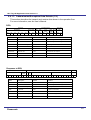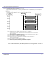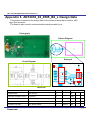
1
アプリケーションノート Application note Part No. MN63Y1208 Package Code No. QFN016-P-0304C Publication date: October 2013 Ver. 1.4 NFC Tag LSI Application Note Version 1.4 Trademark Usage •Wi-Fi is a registered trademark of the Wi-Fi Alliance. •Bluetooth is a registered trademark of the Bluetooth SIC, Inc. •FeliCa is a trademark of Sony Corporation. •FeliCa is the contactless IC card technology developed by Sony Corporation. •Windows is a registered trademark of Microsoft Corporation in the United States and other countries. •Android is a trademark of Google Inc. ・Eclipse is a trademark of Eclipse Foundation, Inc. •MIFARE is a trademark of NXP Semiconductors. •Osaifu-Keitai is a trademark or registered trademark of NTT DOCOMO, INC. in Japan and/or other countries. •'taspo' is a registered trademark of the Tobacco Institute of Japan. •Suica is a registered trademark of East Japan Railway Company. •Edy is a registered trademark of Rakuten Edy, Inc. •All other trademarks are the property of their respective owners. Panasonic NFC Tag LSI Application Note Version 1.4 Contents(1/2) Chapter 1 Introduction 1.1 Purpose 1.2 Organization ……………………… ……………………… P4 P4 2.1 Overview ……………………… 2.2 Key Applications ……………………… 2.3 List of Specifications ……………………… 2.4 Features ……………………… 2.4.1 Three Communication Modes ……………………… 2.4.1.1 RF Communication Mode ……………………… 2.4.1.2 Serial Communication Mode ……………………… 2.4.1.3 Tunnel Communication Mode ……………………… 2.4.2 Functionality to Reduce Power and Utilize Interfaces Flexibly ... 2.4.2.1 Batteryless Communication ……………………… 2.4.2.2 Built-in Non-volatile Memory ……………………… 2.4.2.3 Interrupt from RF Signal ……………………… 2.4.3 High Functionality ……………………… 2.4.3.1 Encryption ……………………… 2.4.3.2 NDEF Format ……………………… 2.5 Hardware Configuration ……………………… 2.5.1 Internal Configuration of the LSI ……………………… 2.5.2 Pin Configuration ……………………… P5 P5 P6 P6 P6 P7 P7 P7 P8 P8 P8 P8 P8 P8 P8 P9 P9 P9 Chapter 2 About NFC Tag LSI Chapter 3 Designing NFC Tag System Hardware 3.1 3.2 3.3 3.4 3.5 Hardware Design Flow Determining the System Configuration Determining the Block Configuration Designing the NFC Tag Block Circuit Designing the NFC Tag Block Pattern ……………………… ……………………… ……………………… ……………………… ……………………… P10 P10 P11 P12 P13 Chapter 4 Designing NFC Tag System Software 4.1 4.2 4.3 4.4 Software Required for NFC Tag RF Communication Mode Operation Flow Serial Communication Mode Operation Flow Tunnel Communication Mode Operation Flow Panasonic ……………………… ……………………… ……………………… .…………………….. P14 P15 P16 P17 2 NFC Tag LSI Application Note Version 1.4 Contents(2/2) Chapter 5 Operation Examples 5.1 Operation Examples Details 5.2 Hardware Conditions 5.3 Access to the User Area 5.3.1 Access from the Host Controller (Serial) 5.3.1.1 Operation Flow Details 5.3.2 Access from Smartphone (FeliCa) 5.3.2.1 Operation Flow Details 5.3.2.2 Transmission/Reception Data Details 5.3.3 Access from Smartphone (TYPE-B) 5.3.3.1 Operation Flow Details 5.3.3.2 Transmission/Reception Data Details 5.4 Tunnel Mode Operation 5.4.1 Operation from Smartphone (FeliCa) 5.4.1.1 Operation Flow Details 5.4.1.2 Transmission/Reception Data Details 5.4.1 Operation from Smartphone (TYPE-B) 5.4.2.1 Operation Flow Details 5.4.2.2 Transmission/Reception Data Details 5.5 Specifying System Area 5.5.1 Setting from Host Controller (Serial) 5.4.1.1 Operation Flow Details 5.5.2 Setting from Smartphone (FeliCa) 5.4.1.1 Operation Flow Details 5.4.1.2 Transmission/Reception Data Details 5.5.3 Setting from Smartphone (TYPE-B) 5.4.1.1 Operation Flow Details 5.4.1.2 Transmission/Reception Data Details …………………….. …………………….. …………………….. …………………….. …………………….. …………………….. …………………….. …………………….. …………………….. …………………….. …………………….. …………………….. …………………….. …………………….. …………………….. …………………….. …………………….. …………………….. …………………….. …………………….. …………………….. …………………….. …………………….. …………………….. …………………….. …………………….. …………………….. P18 P18 P19 P20 P21 P24 P25 P26 P29 P30 P31 P34 P35 P36 P40 P43 P44 P45 P48 P49 P50 P52 P53 P54 P57 P58 P59 Appendix Appendix 1 RF Communication Demonstration ……………………… Appendix 2 Serial Communication Demonstration ……………………… Appendix 3 Tunnel Communication Demonstration ……………………… Appendix 4 Environment to Provide Application Software for Smartphone Appendix 5 BTPB-101B design data ……………………… Appendix 6 ANT4030_02_0505_B0_L design data ……………………… Appendix 7 List of a related documents and hardware ………………… P62 P66 P67 P68 P70 P72 P73 Panasonic 3 NFC Tag LSI Application Note Version 1.4 1. Introduction 1.1 Purpose This is an introduction guide for the NFC Tag LSI, which covers the following. ・Introduction and Overview of NFC Tag LSI ・Information necessary for setting up a system with the NFC Tag LSI This includes typical usage examples. When using this chip in your own environment, refer to the reference data that are introduced in this document. 1.2 Organization This document is organized as follows: About NFC Tag LSI 2 About NFC Tag LSI 2.1 Overview 2.2 Key Applications 2.3 List of Specifications 2.4 Features 2.5 Hardware Configuration Designing NFC tag system hardware 3 Designing NFC Tag System Hardware 3.1 Hardware Design Flow 3.2 Determining the System Configuration 3.3 Determining the Block Configuration 3.4 Designing the NFC Tag Block Circuit 3.5 Designing the NFC Tag Block Pattern Designing NFC tag system software 4 Designing NFC Tag System Software 4.1 Software Required for NFC Tag 4.2 RF Communication Mode Operation Flow 4.3 Serial Communication Mode Operation Flow 4.4 Tunnel Communication Mode Operation Flow Operation examples of NFC tag system Panasonic 5.1 5.2 5.3 5.4 5.5 Operation Examples Details Hardware Conditions Access to the User Area Tunnel Mode Operation Specifying System Area 4 NFC Tag LSI Application Note Version 1.4 2 About NFC Tag LSI 2.1 Overview NFC-tag LSI is an NFC tag LSI, which is capable of communication with smartphone or other reader/writers. It features built-in RF interface and wired serial interface, and includes a non-volatile memory that allows bidirectional access. This LSI allows existing applications to easily perform RF communication. In other words, mounting the NFC tag LSI in various applications enables them to be connected each other through NFC communication. NFC Tag Implementation Examples Game Audio-Visual Device Network Server NFC Tag LSI Camera PC Tablet Smartphone Healthcare Equipment Meter Home Appliances Printer Office Equipment 2.2 Key Applications The NFC tag LSI intends for audio-visual devices, home appliances, and other applications. When this LSI is mounted in various applications, the following operations are allowed using smartphone or other reader/writers. Controlling home appliances and audio-visual devices from smartphone Smartphone can read/write information from/to applications with built-in NFC tag LSI. When the application is in error state, the error is reported using the data stored in the built-in non-volatile memory. This LSI’s built-in non-volatile memory allows data to be read/written from/to a smartphone while the application’s battery is off. Fast data communication with handover Only paring is performed in NFC communication and high capacity data communication is allowed in Bluetooth and Wi-Fi. Panasonic 5 NFC Tag LSI Application Note Version 1.4 2.3 List of Specifications The NFC Tag LSI has a functionality optimized for RF interface implementation on applications. Its key specifications are listed in the table below. List of Specifications Function NFC tag LSI Part No. MN63Y1208 MN63Y1210 Package QFN16/WLCSP SSOP16 1.7 V to 3.6 V 1.8 V to 5.5 V Operating voltage Built-in non-volatile memory 4 kbits FeRAM Supported communication specification RF communicat ion ISO/IEC14443 TYPE-B, JIS X 6319-4 (FeliCa) NFC Forum tag Type4, Type3 Batteryless communication Yes Encryption Wired communicat ion Type3 Interface specification Yes (AES) No I2C (20kHz to 100 kHz) CLK Synchronous Serial (Up to 1MHz)/ UART(Up to 38.4kbps) Interrupt Yes RF and wired direct communications Yes (tunnel communication mode) 2.4 Features Based on the list of specifications described in Section 2.3, this section provides the features of NFC Tag LSI . 2.4.1 Three Communication Modes The NFC Tag LSI allows itself or its application’s host controller to perform the following data communications with smartphone or other reader/writers. RF communication mode: Reader/Writer NFC Tag LSI Serial communication mode: Host controller NFC Tag LSI Tunnel communication mode: Reader/Writer Host controller Relationship between Three Communication Modes Reader/Writer Tunnel Mode Communication RF Panasonic Co m n m un ic ati on NFC Tag LSI lC ria Se om mu o ati nic Host Controller Application 6 NFC Tag LSI Application Note Version 1.4 2.4.1.1 RF Communication Mode The NFC Tag LSI supports 2 RF communication standards: ISO/IEC14443 TTPE-B and JIS X 6319-4 (FeliCa). The standards above are typical in the world of communication, so the NFC Tag LSI supports applications for global market. The area enclosed by a red line in the table below shows the NFC standards supported by the NFC Tag LSI . standards supported by NFC Tag LSI International standard NFC-IP2 ISO/IEC21481 NFC-IP1 ISO/IEC18092 ISO/IEC 14443A (TYPE-A) JIS X 6319-4 Frequency 13.56 MHz Communication distance Up to 10 cm NFC operation mode Upper middleware for encryption, etc. Application ISO/IEC 14443B (TYPE-B) ISO/IEC 15693 Up to 70 cm Card Reader/Writer P2P Mifare FeliCa IC telephone card TASPO Suica, Edy Mobile wallet Basic resident register Driver’s license Baggage for air travel 2.4.1.2 Serial Communication Mode The NFC Tag LSI is compatible with I2C that is typical as a serial communication interface with host controller. The specifications of I2C supported is as follows: Operating frequency: 100 kHz Operating mode: Slave mode Data format: 7-bit addressing 2.4.1.3 Tunnel Communication Mode Operation mode used when performing direct data communication between reader/writer and application’s host controller via the NFC Tag LSI . In this mode, reader/writer accesses the virtual memory area of the host controller. Panasonic 7 NFC Tag LSI Application Note Version 1.4 2.4.2 Functionality to Reduce Power and Utilize Interfaces Flexibly The NFC Tag LSI has a functionality to minimize standby power and utilize both RF and serial communication interfaces flexibly. 2.4.2.1 Batteryless Communication The NFC Tag LSI can operate as a non-volatile memory while no power is supplied from its application. (An alternating magnet field from a sender produces the power necessary for operating the LSI.) The NFC Tag LSI can add RF communication function to applications without increasing standby power. It can also operates even while its application’s power is off. 2.4.2.2 Built-in Non-volatile Memory The NFC Tag LSI has a built-in ferroelectric memory (FeRAM) of 4 kbits as non-volatile memory. The memory allows for RF and serial communications with time lag. For example, data, which is written to the NFC Tag LSI’s built-in memory from a reader/writer while the application’s power is off, can be read by the host controller when the application’s power is turned on. 2.4.2.3 Interrupt from RF Signal It is possible to output an interrupt signal to the host controller, based on RF signal. This function can be used even in batteryless communication. For example, a reader/writer can control the system’s power-on wirelessly. Interrupt signal generation conditions can be set in the NFC Tag LSI’s non-volatile memory. 2.4.3 High Functionality The NFC Tag LSI also has a functionality to meet higher usage requirements. 2.4.3.1 Encryption RF communication is vulnerable to interception because signals travel outside of applications. In order to address this issue, this LSI provides AES encryption for RF communication. 2.4.3.2 NDEF Format The NFC Tag LSI supports the NDEF data format specified in the NFC Forum tag. The support for the standard data format allows a link to certain URL and other settings for a wide variety of NFC-enabled devices. Panasonic 8 NFC Tag LSI Application Note Version 1.4 2.5 Hardware Configuration 2.5.1 Internal Configuration of the LSI The hardware of MN63Y1208 includes the following functional blocks. Analog block: RF interface circuit, power circuit, clock generation circuit Logic block: Control circuit, encryption circuit, I2C interface circuit FeRAM block: 4-kbit FeRAM (Ferroelectric memory) SRAM block: 2-kbit SRAM MN63Y1210 does not have encryption circuit and I2C interface circuit, but instead contains UART and CLK synchronous serial interface circuit. Picture of MN63Y1208 Chip NFC Tag Block 4kbit FeRAM Analog Logic Encryption Analog Serial Logic 2kbit SRAM Control FeRAM SRAM 2.5.2 Pin Configuration The pin information on MN63Y1208 and MN63Y1210 are as follows: Pin configuration and package of MN63Y1208 QFN16 Panasonic Pin configuration and package of MN63Y1210 SSOP16 9 NFC Tag LSI Application Note Version 1.4 3. Designing NFC Tag System Hardware This chapter describes the design of an NFC tag system hardware with MN63Y1208. 3.1 Hardware Design Flow The flow of designing a hardware is summarized below. Subsequent descriptions follow this design flow. Hardware Design Flow Determine the system configuration Determine the block configuration Circuit design Pattern design 3.2 Determining the System Configuration First, determine the system configuration based on requirements for NFC tag system and the communication mode of the NFC tag LSI. A typical system configuration example used in this document is illustrated below. NFC Tag System Configuration Example NFC Tag Block Host Controller Block Host Controller LSI I2C Reader/Writer Antenna Block RF MN63Y1208 Antenna The figure above is based on all communication modes. The blocks required vary with the communication mode used. ・I2C communication: Host control block, NFC tag block (LSI) ・RF communication: Reader/Writer, NFC tag block (LSI, antenna) ・Tunnel mode communication: Reader/Writer, host control block, NFC tag block (LSI, antenna) Panasonic 10 NFC Tag LSI Application Note Version 1.4 3.3 Determining the Block Configuration Next, determine the basic block configuration. Required functions and hardware examples by block are as follows: Required Functions and Hardware Example by Block Block Required Functions Necessary Hardware Host control Interface voltage: 1.7 V to 3.6 V I2C communication function (100 kHz) (NFC Tag LSI power supply control signal) (Interrupt function) Microcontroller NFC tag LSI I2C signal processing, RF signal processing MN63Y1208 tag LSI, and peripheral components Antenna RF signal reception Antenna, and capacitor for resonant frequency adjustment NFC Forum -compliant communication Smartphone with built-in NFC function Reader/Writer Host control block: Select the controller supporting the following functions. I/O voltage: 1.8 V or 3.3 V I2C communication function (As needed) GPIO with a high output current capacity of at least 500 A for battery off (As needed) interrupt function for detecting interrupt from RF signal LSI of NFC tag block: NFC tag LSI and peripheral components are required. For more information, see Section 3.4. Antenna of NFC tag block: Adjusted antenna and resonant capacitor are required. For more information, see the separate Antenna Design Guide. Reader/Writer: Reader/Writer for NFC communication For Reference: We provide a demonstration environment, in which block configuration is as follows: Host control block: Host board with our on-board microcontroller (MN101EF63G) NFC tag block: ANT4030_02_0505_B0_L (our NFC tag board) For reference circuit, see Section 3.4. LSI: For more information, see Section 3.4. Antenna: Our antenna board for demonstration Application software for reader/writer: Android application software for smartphone Panasonic 11 NFC Tag LSI Application Note Version 1.4 3.4 Designing the NFC Tag Block Circuit A circuit diagram example using MN63Y1208 is shown below. For information about antenna block, see the separate Antenna Design Guide. For information about connections, see the figure below. For information about the tag LSI’s peripheral components, see the table below. Circuit Diagram Example of LSI Block of NFC Tag Block LSI Block Host Controller Antenna Block NC TEST1 VDDD NC Host Control Block 3.3 V SCL SDA NIRQ TEST3 SCL SDA NIRQ GPIO R2 R1 R3 8 9 10 11 7 6 5 MN63Y1208 C2 4 3 2 1213 14 15 16 1 VA VSS VDDEX VB C4 C3 VDDA R0 TEST2 TEST4 NC Our NFC Tag Board “ANT4030_02_0505_B0_L” NFC Tag LSI’s Peripheral Components External Components R1, R2 Recommended Value Description 3.3 k Pullup resistors for I2C signal line Determine the values based on data rate, wiring capacitance, and current capacity. Unmounted on our NFC tag board “ANT4030_02_0505_B0_L.” R3 3.3 k Pullup resistor for interrupt signal line Determine the values based on wiring capacitance and current capacity. Unmounted on our NFC tag board “ANT4030_02_0505_B0_L.” C2, C3, C4 0.1 F Capacitors between power supplies for stabilizing the tag LSI operation. Their values are fixed. C2 is connected to VDDD; C3 to VDDA, C4 to VDDEX. R0 100 k Pullup resistor to prevent the undefined state of SCL leading to malfunction. Necessary when R1 is connected to the NFC tag LSI. Note: R1, R2, and R3 on the tag LSI’s peripheral circuit is unnecessary for RF communication. When using our NFC tag board “ANT4030_02_0505_B0_L,” mount these resistors on the host control block side of the board. Panasonic 12 NFC Tag LSI Application Note Version 1.4 3.5 Designing the NFC Tag Block Pattern In designing a pattern of the NFC tag block, the antenna block and LSI block must be combined. This section describes the LSI block. For information on the antenna block, see the separate Antenna Design Guide. When designing a pattern of the LSI block, keep in mind the following precautions. Place capacitors C2, C3, and C4 within 20 mm from the chip. (For resistors R1, R2, and R3, there is no problem to exceed this limit.) An example of the pattern for the NFC tag evaluation board “ANT4030_02_0505_B0_L” we provide is shown below. NFC Tag Pattern Example “ANT4030_02_0505_B0_L” “ANT4030_02_0505_B0_L” is printed on the reverse side of this board Antenna Block LSI Block R0 Enlarged LSI Block To be connected with a separate board C2 VDDEX NIRQ R2 SDA MN63Y1208 R3 SCL R1 VSS C4 C3 Panasonic 13 NFC Tag LSI Application Note Version 1.4 4. Designing NFC Tag System Software 4.1 Software Required for NFC Tag Host Controller Serial Communication NFC Tag LSI Antenna RF Communication Smartphone Tunnel Communication (NFC-enabled) Software for the host controller to control the NFC tag Application software for smartphone To operate an NFC tag, a software for the host controller to control the NFC tag and an application software for smartphone (Reader/Writer) are required. The NFC tag system has 3 communication modes, each of which requires different software. RF communication mode: Application software for smartphone See Section 4.2. Serial communication mode: Software for the host controller to control the NFC tag See Section 4.3. Tunnel communication mode: Both software described above See Section 4.4. Panasonic 14 NFC Tag LSI Application Note Version 1.4 4.2 RF Communication Mode Operation Flow Host Controller NFC Tag LSI Antenna RF Communication Smartphone (NFC-enabled) Application software for smartphone In RF communication mode, even if no voltage is supplied to the NFC tag LSI, generating a magnetic field from a smartphone (Reader/Writer) activates the NFC tag, allowing the smartphone to access the NFC tag LSI’s built-in FeRAM. The figure below illustrates the operation flow of the smartphone and the NFC tag. Host Controller Smartphone NFC Tag No. 1 No. 2 RF Communication Mode Command Response to RF Communication Mode Command No. 1: Smartphone sends an RF communication mode command to the NFC tag. No. 2: The NFC tag receives the RF communication mode command sent in Step No. 1, process it in the tag LSI, and then sends the processing results to the smartphone as a response to the RF communication mode command. We provide sample demonstration application software for smartphone. For detailed settings and operations, refer to the source code of the sample software. In addition, for an outline of how to use the sample demonstration software, see the Appendix. Panasonic 15 NFC Tag LSI Application Note Version 1.4 4.3 Serial Communication Mode Operation Flow Serial Communication Host Controller VDDEX NIRQ I2C Antenna NFC Tag LSI 2 Smartphone (NFC-enabled) Software for the host controller to control the NFC tag In serial communication mode, supplying a power from the host controller activates the NFC tag, allowing the host controller to access the NFC tag LSI’s built-in FeRAM. The figure below illustrates the operation flow of the host controller and the NFC tag. Host Controller No. 1 No. 2 No. 3 NFC Tag Smartphone Apply a Power to VDDEX. Serial Communication Mode Command Response to serial communication mode command No.1: Apply a power to VDDEX pin and then wait at least 3 ms for a serial communication mode command to be issued in Step No. 2. (See parameter E1 of the Product Standards.) No.2: The host controller sends an serial communication mode command to the NFC tag. No.3: The NFC tag receives the serial communication mode command sent in Step No. 2, process it in the NFC tag LSI, and then sends the processing results to the host controller as a response to the serial communication mode command. We provide sample demonstration software for host controller. For detailed settings and operations, refer to the source code of the sample software. In addition, for an outline of how to use the sample demonstration software, see the Appendix. Panasonic 16 NFC Tag LSI Application Note Version 1.4 4.4 Tunnel Communication Mode Operation Flow Host Controller VDDEX NIRQ I2C NFC Tag LSI Antenna RF Communication 2 Tunnel Communication Software for the host controller to control the NFC tag Smartphone (NFC-enabled) Application software for smartphone Using the tunnel communication mode allows communication between the host controller and a smartphone via the NFC tag, however requiring the following: software for the host controller and application software for smartphone. The figure below illustrates the operation flow in tunnel communication mode. Host Controller NFC Tag Interrupt Request (IRQ) No. 2 Apply a Power to VDDEX. Smartphone Tunnel Communication Mode Command No. 1 No. 3 QUERY Command No. 4 Response to the QUERY Command No. 5 No. 6 ANSWER Command Response to the ANSWER Command No. 7 Response to Tunnel Communication Mode Command No. 8 No. 1: Smartphone sends a tunnel communication mode command to the NFC tag. No. 2: The NFC tag receives the tunnel communication mode command and then sends an Interrupt request (IRQ) to the host controller. No. 3: When a power is not applied to VDDEX pin, the host controller applies it to the pin. No. 4: The host controller sends a QUERY command to the NFC tag. No. 5: The NFC tag sends a response to the QUERY command to the host controller. No. 6: The host controller sends an ANSWER command to the NFC tag to report the results. No. 7: The NFC tag receives the ANSWER command and then sends a response to the command to the host controller. No. 8: Following the response in Step No. 7, the NFC tag sends the content of the ANSWER command to smartphone as a response to the tunnel communication mode command. We provide sample demonstration software for host controller and sample demonstration application software for smartphone. For detailed settings and operations, refer to the source code of the sample software. In addition, for an outline of how to use those software, see the Appendix. Panasonic 17 NFC Tag LSI Application Note Version 1.4 5. Operation Examples This chapter specifically describes the operations of a system with NFC tag, which uses hardware described in Chapter 3 and software described in Chapter 4. Unless otherwise specified, MN63Y1208 is used for these examples. 5.1 Operation Example Details To describe the operation examples, the following sections are provided. ・5.3 Access to the User Area Access from host controller (serial) and smartphone (FeliCa, TYPE-B) ・5.4 Tunnel Mode Operation Operation with smartphone (FeliCa, TYPE-B) ・5.5 Specifying System Area Setting with host controller (serial) and smartphone (FeliCa, TYPE-B) 5.2 Hardware Conditions This operation examples use the following hardware examples and connection examples. Devices Used in this Examples Block Devices used Description Comment Host controller Our demonstration board: BTPB-101B A device with built-in host controller that is accessible to NFC tag in serial communication See the Appendix 5, “BTPB-01B Specification.” NFC tag Tag antenna board: ANT4030_02_0505_B0_L (With on-board MN63Y1208) A board on which the NFC tag LSI and components for interface are implemented See the Appendix 6 “ANT4030_02_0505_B0_ LSpecification.” Reader/Writer AndroidOS smartphone supporting NFC A device to access a tag in RF communication - Connection Example Smartphone (Reader/Writer) NFC tag ANT4030_02_0505_B0_L CN1 RF (MINI-USB) Host Controller Host Control Block BTPB-101B I2C CN2 Reverse the ANT4030_02_0505_B0_L and connect it to the CN2 (white connector) of the BTPB-101B. Power is supplied to the BTPB-101B through CN1. In this demonstration environment, the PC controls the BTPB-101B to simplify the access to the NFC tag. Panasonic 18 NFC Tag LSI Application Note Version 1.4 5.3 Access to the User Area This section uses a simple example to describe how to access an NFC tag. Since FeliCa uses 16 bytes, and TYPE-B and serial communication use 1 byte for each access, the following communication process is applied. Communication Process FeliCa Write a data of 0xA5A5A5A5A5A5A5A5A5A5A5A5A5A5A5A5 to the block 0(the addresses of 0x000 to 0x00F) of the NFC tag. ↓ Read data from the block 0(the addresses of 0x000 to 0x00F) of the NFC tag. Serial, TYPE-B Write a data of 0xA5 to the address 0x0000 of the NFC tag. ↓ Read data from the address 0x0000 of the NFC tag In the initial state of NFC tag, the following three communication modes are available: RF communication (FeliCa, TYPE-B) and serial communication. However, using the subsequent setting, you can restrict communication. In such a case, note that a certain communication may be disabled. Panasonic 19 NFC Tag LSI Application Note Version 1.4 5.3.1 Access from the Host Controller (Serial) The serial communication between the NFC tag with MN63Y1208 and the host controller is compliant with the I2C specification. Its corresponding protocol is as follows: 7-bit addressing mode and operating frequency of 100 kHz. The outline of the operation flow is shown in the figure below. Outline of Operation Flow Host NFC Tag Smartphone Controller SNo.1 Apply a Power to VDDEX. SNo.2 WRITE Command SNo.3 Write Complete Flag SNo.4 Response to the WRITE Command SNo.5 READ Command SNo.6 Read Ready Complete Flag SNo.7 Read Data SNo.1: Apply a power to VDDEX pin and then wait 3 ms for a command to be received. (See parameter E1 of the Product Standards.) SNo.2: The host controller sends a WRITE command to the NFC tag. After receiving the command, the NFC tag processes the command. SNo.3: After completing the command processing, the NFC tag returns an NIRQ as a write complete flag. SNo.4: The NFC tag sends the processing results to the host controller as a response to the write command. SNo.5: The host controller sends a READ command to the NFC tag. After receiving the command, the NFC tag processes the command. SNo.6: After completing the command processing, the NFC tag returns an NIRQ as a read ready complete flag. SNo.7: the NFC tag sends a read data to the host controller as a response to the read command. Panasonic 20 NFC Tag LSI Application Note Version 1.4 5.3.1.1 Operation Flow Details (1/3) SNo.1 SNo. The detailed operation flow is shown in the figure below. Flowchart Outline Turn on VDDEX (power supply for NFC tag). Host Controller 3 ms Start transmission. Send a start bit, 7bit slave address of 0x54, and WR of 0. Receive ACK. Send a WRITE command of 0x18. SNo.2 Receive ACK. 0xA8 Send the address of 0x0000 In twice. Send ACK. SDA Data valid period Send ACK. Data change period Start bit and stop bit change SDA when SLC = high. Start bit SCL 0x00 SDA ACK Send ACK. Stop bit Send ADDR_L. 0x00 ACK Send a transmit data length (LEN) of 0x01. SCL 0x18 ACK Send ADDR_H. Receive ACK for each transmission. Normal data transmission Start Bit ACK Send a command. Comment for I2C communication In I2C-bus communication, normally SDA is changed when SCL = low. Start bit and stop bit produce special patterns as shown below. VDDEX = High Power ON Wait 3 ms. Start communication. NFC Tag Send LEN. SCL Send ACK. 0x01 ACK: Same as data of 0 NACK: Same as data of 1 Receive ACK. ACK SDA Send ACK. To be continued to the next page Panasonic 21 NFC Tag LSI Application Note Version 1.4 SNo. 5.3.1.1 Operation Flow Details (2/3) Flowchart Outline Host Controller NFC Tag Continued from the previous page SNo.2 Send a WRITE data of 0xA5. Receive ACK. Send a data. 0xA5 ACK NIRQ = Low Monitor NIRQ. Start transmission. Send a start bit, 7bit slave address of 0x54, and WR of 1. Start communication. Send a start bit, 7bit slave address of 0x54, and WR of 0. Send NACK and stop bit. Start transmission. Receive ACK. 0xA8 ACK Send a command. Send ACK as a response. Stop bit NACK Start bit Notify processing complete. 0xA9 Data of 0x35, 0x25, or 0x15 may be produced depending on the RF signal state. Receive ACK. Send a READ command of 0x08. Start bit ACK 0x05 Receive ACK and STATUS. Send NACK and stop bit. SNo.5 Stop bit Wait for NFC tag to be processed. Start communication. SNo.4 Send a stop bit. Interrupt processing SNo.3 Send a stop bit. Send ACK. Send ACK. 0x08 ACK Send ACK. To be continued to the next page Panasonic 22 NFC Tag LSI Application Note Version 1.4 SNo. 5.3.1.1 Operation Flow Details (3/3) Flowchart Outline Host Controller NFC Tag Continued from the previous page Send the address of 0x0000 in twice. Send ADDR_H. 0x00 Receive ACK for each transmission. SNo.5 Send ADDR_L. 0x00 Send ACK. ACK Send LEN. 0x01 Send a stop bit. Send ACK. ACK Receive ACK. Send a stop bit. Wait for internal processing of the NFC tag to terminate. Stop bit Internal processing Send the required data length (LEN) of 0x01. SNo.6 Send ACK. ACK NIRQ = Low Notify processing is terminated. Monitor NIRQ. Start communication. SNo.7 Send a start bit, 7-bit slave address of 0x54, and WR of 1. Start transmission. Data of 0x35, 0x25, or 0x15 may be produced depending on the RF signal state. Send ACK. After sending ACK, read the data. Send NACK and stop bit. Panasonic 0xA9 ACK 0x05 Receive ACK and STATUS. Receive the data. Start bit ACK 0x01 Send NACK + Stop bit. Send ACK as a response. NACK Send a data. Stop bit 23 NFC Tag LSI Application Note Version 1.4 5.3.2 Access from Smartphone (FeliCa) RF communication between smartphone (FeliCa) and NFC tag is compliant with the JISX6319-4 standard. The data transfer rates supported are 212 kbps and 424 kbps, but anti-collision is not supported. The outline of the operation flow is shown in the figure below. Outline of Operation Flow Host Controller NFC Tag Smartphone REQ Command SNo.1 Response to the REQ SNo.2 WRITE Command SNo.3 Response to the WRITE Command SNo.4 READ Command SNo.5 Response to the READ Command SNo.6 SNo.1: Smartphone sends a REQ command and waits for a response. If NFC tag does not exist, the response to be returned in SNo.2 is not returned and SNo.1 is repeated. SNo.2: The NFC tag returns a response to the REQ command sent in SNo.1. The smartphone recognizes the NFC tag. SNo.3: The smartphone sends a WRITE command. The NFC tag receives the WRITE command and processes it. SNo.4: The NFC tag sends the processing results to the smartphone. SNo.5: The smartphone sends a READ command. The NFC tag receives the READ command and processes it. SNo.6: The NFC tag sends the read data to the smartphone. Note: In Android terminal, the OS supports the processing of SNo. 1 and SNo. 2. Panasonic 24 NFC Tag LSI Application Note Version 1.4 5.3.2.1 Operation Flow Details SNo. The detailed operation flow is shown in the figure below. For waveform specification, see the JISX6319-4 standard. Flowchart Outline SNo.6 SNo.5 SNo.4 SNo.3 SNo.2 SNo.1 NFC Tag Smartphone Send REQ. 0x 00 00 00 00 00 00 B2 4D 06 00 FF FF 00 00 09 21 Seek an NFC tag. Respond to REQ. The NFC tag returns a response. Respond to REQ. Designate the NFC tag and write data. Respond to WRITE. Return a message stating that the NFC tag completed writing normally. Respond to WRITE. Send READ. Respond to READ. Panasonic Respond to READ. Send WRITE. 0x 00 00 00 00 00 00 B2 4D 0C 09 02 FE 00 00 00 00 00 00 00 00 D5 2F 0x 00 00 00 00 00 00 B2 4D 10 06 02 FE 00 00 00 00 00 00 01 09 00 01 80 00 92 4A Designate the NFC tag and read data. Return a message stating that the NFC tag completed reading normally 0x 00 00 00 00 00 00 B2 4D 12 01 02 FE 00 00 00 00 00 00 FF FF 00 00 00 FF FF FF ED CE 0x 00 00 00 00 00 00 B2 4D 20 08 02 FE 00 00 00 00 00 00 01 09 00 01 80 00 A5 A5 A5 A5 A5 A5 A5 A5 A5 A5 A5 A5 A5 A5 A5 A5 93 D3 Send WRITE. Send REQ. Send READ. 0x 00 00 00 00 00 00 B2 4D 1D 07 02 FE 00 00 00 00 00 00 00 00 01 A5 A5 A5 A5 A5 A5 A5 A5 A5 A5 A5 A5 A5 A5 A5 A5 CA 78 25 NFC Tag LSI Application Note Version 1.4 5.3.2.2 Transmission/Reception Data Details (1/3) This section describes the transmit and receive data shown in the operation flow. For more information, see the User’s Manual. REQ Start Field PREAMBLE 00 00 00 00 SYNC CODE 00 00 B2 4D LEN CMD 06 00 Information Field End Field SYS CODE CRC FF REQ SLOT CODE FF 00 00 09 21 Name Description Pattern Comment PREAMBLE Preamble 0x000000000000 Fixed value given when starting communication SYNC CODE Synchronous code 0xB24D Fixed value given when starting communication LEN Information field length 0x06 Byte length of information field CMD Command 0x00 Code of REQ command SYS CODE System code 0xFFFF Responds independent of the system area SC. REQ CODE Request code 0x00 Processed as “no request” SLOT Time slot 0x00 Always set to 00 in this LSI. CRC CRC calculated value 0x0921 CRC calculated value of information field Response to REQ Start Field Information Field PREAMBLE 00 00 00 00 SYNC CODE 00 00 B2 4D LEN CM End Field PICC CODE DATA FIELD CRC D 12 01 02 FE 00 00 00 00 00 00 FF FF 00 00 00 FF FF FF Name Description Pattern Comment PREAMBLE Preamble 0x000000000000 Fixed value given when starting communication SYNC CODE Synchronous code 0xB24D Fixed value given when starting communication LEN Information field length 0x12 Byte length of information field CMD Command 0x01 Response code to REQ PICC CODE PICC identifier 0x02FE000000000000 IDM default value of NFC tag PMM Response time descriptor 0xFFFF000000FFFFFF Time until NFC tag returns a response CRC CRC calculated value 0xEDCE CRC calculated value of information field Panasonic ED CE 26 NFC Tag LSI Application Note Version 1.4 5.3.2.2 Transmission/Reception Data Details (2/3) WRITE Start Field PREAMBLE Information Field SYNC CODE LEN CMD SVS NUM PICC CODE SVS Blk NUM Block List ~ 00 00 00 00 00 00 B2 4D 20 08 02 FE 00 00 00 00 00 00 01 09 00 01 80 00 End Field CRC DATA ~ A5 A5 A5 A5 A5 A5 A5 A5 A5 A5 A5 A5 A5 A5 A5 A5 93 D3 Name Description Pattern Comment PREAMBLE Preamble 0x000000000000 Fixed value given when starting communication SYNC CODE Synchronous code 0xB24D Fixed value given when starting communication LEN Information field length 0x20 Byte length of information field CMD Command 0x08 Code of WRITE command PICC CODE PICC identifier 0x02FE000000000000 IDM default value of NFC tag SVSNUM Number of service files 0x01 Number of service files SVS Service file identifier 0x0900 Service identifier BLK NUM Number of blocks 0x01 Number of write blocks BLK List Block list 0x8000 Specifies write block. DATA Write data 0x A5 A5 A5 A5 A5 A5 A5 A5 Write data A5 A5 A5 A5 A5 A5 A5 A5 CRC CRC calculated value 0x93D3 CRC calculated value of information field Response to WRITE Start Field PREAMBLE Information Field SYNC LEN CMD CODE PICC CODE End Field STATUS CRC 1 2 00 00 00 00 00 00 B2 4D 0C 09 02 FE 00 00 00 00 00 00 00 00 D5 2F Name Description Pattern Comment PREAMBLE Preamble 0x000000000000 Fixed value given when starting communication SYNC CODE Synchronous code 0xB24D Fixed value given when starting communication LEN Information field length 0x0C Byte length of information field CMD Command 0x09 Response code to WRITE command PICC CODE PICC identifier 0x02FE000000000000 IDM default value of NFC tag STATUS1 Status flag 1 0x00 00: Normal termination STATUS2 Status flag 2 0x00 00: Normal termination CRC CRC calculated value 0xD52F CRC calculated value of information field Panasonic 27 NFC Tag LSI Application Note Version 1.4 5.3.2.2 Transmission/Reception Data Details (3/3) READ Start Field PREAMBLE Information Field SYNC LEN CM CODE D PICC CODE SVS NUM SVS Blk NUM Block List End Field CRC 00 00 00 00 00 00 B2 4D 10 06 02 FE 00 00 00 00 00 00 01 09 00 01 80 00 92 4A Name Description Pattern Comment PREAMBLE Preamble 0x000000000000 Fixed value given when starting communication SYNC CODE Synchronous code 0xB24D Fixed value given when starting communication LEN Information field length 0x10 Byte length of information field CMD Command 0x06 Code of READ command PICC CODE PICC identifier 0x02FE000000000000 IDM default value of NFC tag SVSNUM Number of service files 0x01 Number of service files SVS Service file identifier 0x0900 Service identifier BLK NUM Number of blocks 0x01 Number of read blocks BLK List Block list 0x8000 Specifies read block. CRC CRC calculated value 0x924A CRC calculated value of information field Response to READ Start Field Information Field End Field CRC STATUS Blk SYNC LE CM PICC CODE DATA NUM CODE N D 00 00 00 00 00 00 B2 4D 1D 07 02 FE 00 00 00 00 00 00 00 00 01 A5 A5 A5 A5 A5 A5 A5 A5 A5 A5 A5 A5 A5 A5 A5 A5 CA 78 PREAMBLE Name Description Pattern Comment PREAMBLE Preamble 0x000000000000 Fixed value given when starting communication SYNC CODE Synchronous code 0xB24D Fixed value given when starting communication LEN Information field length 0x1D Byte length of information field CMD Command 0x07 Response code to READ command PICC CODE PICC identifier 0x02FE000000000000 IDM default value of NFC tag STATUS1 Status flag 1 0x00 00: Normal termination STATUS2 Status flag 2 0x00 00: Normal termination DATA Read data 0x A5 A5 A5 A5 A5 A5 A5 A5 A5 A5 A5 A5 A5 A5 A5 A5 Read data CRC CRC calculated value 0xCA78 CRC calculated value of information field Panasonic 28 NFC Tag LSI Application Note Version 1.4 5.3.3 Access from Smartphone (TYPE-B) RF communication between smartphone (TYPE-B) and NFC tag is compliant with the ISO/IEC14443 standard. The data transfer rates supported are 106 kbps and 212kbps, but anti-collision is not supported. The outline of the operation flow is shown in the figure below. Outline of Operation Flow Host Controller Smartphone NFC Tag REQB Command SNo.1 Return ATQB. SNo.2 ATTRIB Command SNo.3 Response to the ATTRIB SNo.4 WRITE Command SNo.5 Response to the WRITE Command SNo.6 READ Command SNo.7 Response to the READ Command SNo.8 SNo.1: Smartphone sends a REQB command and waits for a response. If NFC tag does not exist, the response to be returned in SNo.2 is not returned and SNo.1 is repeated. SNo.2: NFC tag returns an ATQB as a response to the REQB command sent in SNo.1. The smartphone recognizes the NFC tag. SNo.3: The smartphone sends an ATTRIB command. SNo.4: The NFC tag returns a response to the ATTRIB command sent in SNo.3. The NFC tag is activated. SNo.5: The smartphone sends a WRITE command. The NFC tag receives the WRITE command and processes it. SNo.6: The NFC tag sends the processing results to the smartphone. SNo.7: The smartphone sends a READ command. The NFC receives the READ command and processes it. SNo.8: The NFC tag sends the read data to the smartphone. Note: In Android terminal, the OS supports the processing of SNo. 1 to SNo. 4. Panasonic 29 NFC Tag LSI Application Note Version 1.4 5.3.3.1 Operation Flow Details The detailed operation flow is shown in the figure below. For waveform specification and SOF/EOF patterns, see the ISO/IEC14443 standard. Data is sent in units of 10 bits, to which values of 0 and 1 have been given as the first and last bits, respectively, in units of 8 bytes. These specifications are also specified in the ISO/IEC 14443 standard. SNo. Send REQB. NFC Tag Seek an NFC tag. Return ATQB. The NFC tag returns a response. Send WRITE. SNo.7 SNo.6 SNo.4 Select the NFC tag. Respond to ATTRIB. SNo.8 Return ATQB. Smartphone SOF 0x 05 00 00 71 FF EOF SOF 0x 50 00 00 00 00 00 00 00 00 91 81 E0 D9 83 EOF Send ATTRIB. SNo.5 SNo.3 SNo.2 Outline SNo.1 Flowchart The NFC tag has been selected. Respond to ATTRIB. Designate the NFC tag and write data. Respond to WRITE. Return a message stating that the NFC tag completed writing normally. Respond to WRITE. SOF 0x 1D 00 00 00 00 00 00 01 00 79 5A EOF SOF 0x 10 F9 E0 EOF SOF 0x 02 00 D6 00 00 01 A5 1B 94 EOF SOF 0x 02 90 00 29 6A EOF SOF 0x 03 00 80 00 00 01 E7 8B EOF SOF 0x 03 A5 90 00 24 F6 EOF Send READ. Designate the NFC tag and read data. Respond to READ. Return a message stating that the NFC tag completed reading normally. Panasonic Respond to READ. Send REQB. Send ATTRIB. Send WRITE. Send READ. 30 NFC Tag LSI Application Note Version 1.4 5.3.3.2 Transmission/Reception Data Details (1/3) REQB CMD AFI PAR CRC AM SOF 05 00 EOF 00 71 FF Name Description Pattern Comment CMD Command 0x05 REQB/WUPB command AFI Application Family Identifier 0x00 Overall response. See the ISO/IEC14443 standard. PARAM Parameter 0x00 Selects REQB. CRC CRC calculated value 0x71FF CRC calculated value ATQB (Response to REQB) RES SOF PUPI Application Data Protocol Info CRC CODE 50 EOF 00 00 00 00 00 00 00 00 91 81 E0 D9 83 Name Description Pattern Comment RES CODE Response code 0x50 ATQB (response to REQB) PUPI PICC identifier 0x00000000 Lower 4 bytes of IDM Application Data Application Data 0x00000000 Not used Protocol Info Protocol Info 0x9181E0 Parameter. See the User’s Manual. CRC CRC calculated value 0xD983 CRC calculated value ATTRIB CMD PARAM Identifier SOF 1D 00 00 00 00 CRC 1 2 3 4 00 00 01 00 EOF 79 5A Name Description Pattern Comment CMD Command code 0x1D ATTRIB command Identifier PICC identifier 0x00000000 Specifies the PUPI of ATQB. PARAM1 Parameter 1 0x00 See the User’s Manual. PARAM2 Parameter 2 0x00 See the User’s Manual. PARAM3 Parameter 3 0x01 See the User’s Manual. PARAM4 Parameter 4 0x00 See the User’s Manual. CRC CRC calculated value 0x795A CRC calculated value Panasonic 31 NFC Tag LSI Application Note Version 1.4 5.3.3.2 Transmission/Reception Data Details (2/3) Response to ATTRIB RES SOF CRC CODE EOF 10 F9 E0 Name Description Pattern Comment RES CODE Response code 0x10 Response to ATTRIB CRC CRC calculated value 0xF9E0 CRC calculated value WRITE PCB CLA INS Address D6 00 LEN DATA SOF 00 02 00 01 A5 CRC 1B EOF 94 Name Description Pattern Comment PCB Protocol Control Byte 0x02 I-block CLA CLA 0x00 Class byte; fixed value INS WRITE 0xD6 Instruction byte; WRITE = 0xD6 Address Start address 0x0000 Address at which to start writes LEN Data length 0x01 Write data length (byte) Data Write data 0xA5 Write data CRC CRC calculated value 0x1B94 CRC calculated value Response to WRITE SOF PCB 02 SW 1 2 90 00 CRC 29 EOF 6A Name Description Pattern Comment PCB Protocol Control Byte 0x02 I-block SW1 Status word 1 0x90 0x9000: No error SW2 Status word 2 0x00 CRC CRC calculated value 0x296A Panasonic CRC calculated value 32 NFC Tag LSI Application Note Version 1.4 5.3.3.2 Transmission/Reception Data Details (3/3) READ PCB CLA INS Address B0 00 LEN SOF 03 00 00 01 CRC E7 EOF 8B Name Description Pattern Comment PCB Protocol Control Byte 0x03 I-block CLA CLA 0x00 Class byte; fixed value INS READ 0xB0 Instruction byte; READ = 0xB0 Address Start address 0x0000 Address at which to start reads LEN Data length 0x01 Read data length (byte) CRC CRC calculated value 0xE78B CRC calculated value Response to READ SOF PCB DATA 03 A5 SW 1 2 90 00 CRC 24 EOF F6 Name Description Pattern Comment PCB Protocol Control Byte 0x03 I-block Data Read data 0xA5 Read data SW1 Status word 1 0x90 0x9000: No error SW2 Status word 2 0x00 CRC CRC calculated value 0x24F6 Panasonic CRC calculated value 33 NFC Tag LSI Application Note Version 1.4 5.4 Tunnel Mode Operation This section specifically describes how to access between the host controller and smartphone through an NFC tag while in Tunnel mode. For information about Tunnel mode, see Section 4.4. Since FeliCa uses 16 bytes, and TYPE-B uses 1 byte for each access, the following communication process is applied. Detail of Communication FeliCa Write a data of 0xA5A5A5A5A5A5A5A5A5A5A5A5A5A5A5A5 to the block 0(the addresses of 0x0000 to 0x000F) of the host controller. ↓ Read data from the block 0(the addresses of 0x0000 to 0x000F) of the host controller. TYPE-B Write a data of 0xA5 to the address 0x0000 of the host controller. ↓ Read data from the address 0x0000 of the host controller. In the initial state of NFC tag, the following three communication modes are available: RF communication (FeliCa, TYPE-B) and serial communication. However, using the subsequent setting, you can restrict communication. In such a case, note that a certain communication may be disabled. Panasonic 34 NFC Tag LSI Application Note Version 1.4 5.4.1 Operation from Smartphone (FeliCa) The outline of the operation flow is shown in the figure below. Host Controller NFC Tag SNo.4 IRQ Notification SNo.5 Apply a power to VDDEX. SNo.6 QUERY Command SNo.7 SNo.8 SNo.9 SNo.1 Response to the REQ SNo.2 Tunnel WRITE Command SNo.3 ANSWER Command Response to the ANSWER Command IRQ Notification SNo.13 QUERY Command SNo.14 Response to the QUERY Command SNo.16 REQ Command Response to the QUERY Command SNo.12 SNo.15 Smartphone Response to the Tunnel WRITE Command SNo.10 Tunnel READ Command SNo.11 Response to the Tunnel READ Command SNo.17 ANSWER Command Response to the ANSWER Command SNo.1 to SNo.2: Same as for Section 5.3.2. SNo.3: Smartphone sends a Tunnel WRITE command. SNo.4: NFC tag notifies the host controller using NIRQ. SNo.5: Apply a power to VDDEX pin and wait 3 ms for a command to be received. (See parameter E1 of the Product Standards.) SNo.6: The host controller sends a QUERY command to the NFC tag. SNo.7: The NFC tag sends a response to the QUERY command to the host controller. SNo.8: The host controller sends an ANSWER command to the NFC tag to report the results. SNo.9: The NFC tag receives the ANSWER command and then sends a response to the command to the host controller. SNo.10: The NFC tag sends a response to the Tunnel WRITE command to the Smartphone. SNo.11: The smartphone sends a Tunnel READ command. SNo.12 to SNo.16: Same as for SNo.4 and SNo.6 through SNo.9. SNo.17: The NFC tag sends a response to the Tunnel READ command to the smartphone. Panasonic 35 NFC Tag LSI Application Note Version 1.4 5.4.1.1 Operation Flow Details (1/4) SNo.5 SNo.4 SNo.3 SNo.2 SNo.1 SNo. The detailed operation flow is shown in the figure below. Flowchart Outline NFC Tag Smartphone Send REQ. 0x 00 00 00 00 00 00 B2 4D 06 00 FF FF 00 00 09 21 Seek an NFC tag.. Respond to REQ. The NFC tag returns a response. Respond to REQ. Send Tunnel WRITE. Wait for processing of NFC tag to terminate. Turn on VDDEX (power supply for NFC tag) Wait 3 ms. Power ON Start Send a start bit, 7- transmission bit slave address of 0x54, and WR of 0. Receive ACK. Send QUERY command of 0x28. Receive ACK. Send QUERY. Send a stop bit. Start communication. Start Send a start bit, reception. 7-bit slave address of 0x54, and WR of 1. SNo.7 Receive ACK and STATUS. Start bit 0xA8 Return ACK. ACK 0x28 Return ACK. Stop bit Start bit 0xA9 ACK 0x03 Data of 0x33, 0x23, or 0x13 may be produced depending on the RF signal state. Send ACK. Receive address. Send ACK and receive 0x0000 in twice. VDDEX = High ACK Send a stop bit. Send ACK as a response. ACK 0x00 Send ACK. Send Tunnel WRITE. Notify processing is terminated. NIRQ = Low Monitor NIRQ. Send REQ. 0x 00 00 00 00 00 00 B2 4D 12 01 02 FE 00 00 00 00 00 00 FF FF 00 00 00 FF FF FF ED CE 0x 00 00 00 00 00 00 B2 4D 21 08 02 FE 00 00 00 00 00 00 01 09 00 01 00 00 04 A5 A5 A5 A5 A5 A5 A5 A5 A5 A5 A5 A5 A5 A5 A5 A5 46 68 Designate the NFC tag and write data. Start communication. SNo.6 Host Controller Send ADDR_H. ACK To be continued to the next page Panasonic 36 NFC Tag LSI Application Note Version 1.4 5.4.1.1 Operation Flow Details (2/4) SNo. The detailed operation flow is shown in the figure below. Flowchart Outline Host Controller NFC Tag Continued from the previous page Send address. SNo.7 Send ACK and receive 0x0000 in twice. Receive LEN. Transmit ACK and receive a data length of 0x01. Receive a data. Send ACK and receive a data of 0xA5. Smartphone Send ADDR_L. 0x00 Send ACK. ACK Send LEN. 0x10 Send ACK. ACK Send a data. 0xA5 Repeat 16 times. SNo.8 Repeat 16 times. Send NACK and stop bit. Send NACK + stop bit. Start communication. transmission. Start Send a start bit , 7-bit slave address of 0x54, and WR of 0. Receive ACK. Receive ACK. SNo.9 Send a start bit, 7bit slave address of 0x54, and WR of 1. SNo.10 Return a message stating that the NFC tag completed writing normally. Panasonic Send ACK. Send ACK. ACK Stop bit Start bit 0xA9 ACK 0x05 Receive ACK and STATUS. Respond to Tunnel WRITE. 0xA8 0xF8 Send a stop bit. Start Start communication. reception. Send NACK and stop bit. Start bit ACK Send Send ANSWER ANSWER. command of 0xF8. Send a stop bit. Stop bit NACK Data of 0x33, 0x23, or 0x13 may be produced depending on the RF signal state. Send NACK + stop bit. NACK Send ANSWER as a response Stop bit Send Tunnel WRITE. 0x 00 00 00 00 00 00 B2 4D 0C 09 02 FE 00 00 00 00 00 00 00 00 D5 2F To be continued to the next page 37 NFC Tag LSI Application Note Version 1.4 5.4.1.1 Operation Flow Details (3/4) SNo. The detailed operation flow is shown in the figure below. Flowchart Outline Host Controller NFC Tag Smartphone SNo.12 SNo.11 Continued from the previous page Send Tunnel READ. Turn on VDDEX (power supply for NFC tag). Wait 3 ms. Start communication. Send a start bit, 7-bit slave address of 0x54, and WR of 0. Receive ACK. SNo.13 0x 00 00 00 00 00 00 B2 4D 11 06 02 FE 00 00 00 00 00 00 01 09 00 01 00 00 04 82 C7 Designate the NFC tag and read data. Send QUERY command of 0x28. NIRQ = Low Start transmission. Send QUERY. Start communication. SNo.14 Send a start bit, 7-bit slave address of 0x54, and WR of 1. Receive ACK and STATUS. Send a stop bit. Send ACK. Stop bit Start bit 0xA9 ACK 0x01 Send ACK as Data of 0x31, 0x21, or 0x11 a response. may be produced depending on the RF signal state. Send ACK. Receive the address. Send ACK and receive 0x0000 in twice. Send ACK. 0x28 ACK Start reception. Notify processing is terminated 0xA8 ACK Receive ACK. Send a stop bit. Start bit Send Tunnel READ. ACK 0x00 Send ACK. Send ADDR_H. ACK To be continued to the next page Panasonic 38 NFC Tag LSI Application Note Version 1.4 5.4.1.1 Operation Flow Details (4/4) SNo. The detailed operation flow is shown in the figure below. Flowchart Outline Host Controller Continued from the previous page Receive the address. SNo.14 Send ACK and receive 0x0000 in twice. Receive LEN. Send ACK and receive a data length of 0x01. Send ACK. ACK Start communication. Start transmission. Stop bit NACK Start bit Send a start bit, 7-bit slave address of 0x54, and WR of 0. Receive ACK. SNo.15 Send LEN. 0x10 Send NACK + stop bit. 0xA8 Send ACK. ACK Send ANSWER. 0xF8 Send ACK. ACK Receive ACK. Send a data. Send ACK and then a data of 0xA5. Send ADDR_L. 0x00 Send NACK and stop bit. Send ANSWER command of 0xF8. Send a data. 0xA5 Send ACK. ACK Repeat 16 times. Send a stop bit. Send a stop bit. SNo.16 Repeat 16 times Stop bit Start Start communication. reception. Start bit Send a start bit, 7-bit slave address of 0x54, and WR of 1. Receive ACK and STATUS. 0xA9 ACK 0x05 Respond to Data of 0x33, 0x23, or 0x13 ANSWER. may be produced depending on the RF signal state. Send NACK and stop bit. SNo.17 Smartphone NFC Tag Respond to Tunnel READ. Send a read data from the NFC tag. Panasonic Send NACK + stop bit. NACK Stop bit Send Tunnel READ. 0x 00 00 00 00 00 00 B2 4D 1D 07 02 FE 00 00 00 00 00 00 00 00 01 A5 A5 A5 A5 A5 A5 A5 A5 A5 A5 A5 A5 A5 A5 A5 A5 CA 78 39 NFC Tag LSI Application Note Version 1.4 5.4.1.2 Transmission/Reception Data Details (1/3) This section describes the transmit and receive data shown in the operation flow. For more information, see the User’s Manual. REQ Start Field PREAMBLE 00 00 00 00 SYNC CODE 00 00 B2 LEN CMD 06 00 4D Information Field End Field SYS CODE CRC FF REQ SLOT CODE FF 00 00 09 21 Name Description Pattern Comment PREAMBLE Preamble 0x000000000000 Fixed value given when starting communication SYNC CODE Synchronous code 0xB24D Fixed value given when starting communication LEN Information field length 0x06 Byte length of information field CMD Command 0x00 Code of REQ command SYS CODE System code 0xFFFF Responds independent of the system area SC. REQ CODE Request code 0x00 Processed as “No request.” SLOT Timeslot 0x00 Always set to 00 in this LSI. CRC CRC calculation value 0x0921 CRC calculated value of information field Response to REQ Start Field Information Field PREAMBLE 00 00 00 00 SYNC CODE 00 00 B2 4D LEN CM End Field PICC CODE DATA FIELD CRC D 12 01 02 FE 00 00 00 00 00 00 FF FF 00 00 00 FF FF FF Name Description Pattern Comment PREAMBLE Preamble 0x000000000000 Fixed value given when starting communication SYNC CODE Synchronous code 0xB24D Fixed value given when starting communication LEN Information field length 0x12 Byte length of information field CMD Command 0x01 Response code to REQ PICC CODE PICC identifier 0x02FE000000000000 IDM default value of NFC tag PMM Response time descriptor 0xFFFF000000FFFFFF Time until NFC tag returns a response CRC CRC calculated value 0xEDCE CRC calculated value of information field Panasonic ED CE 40 NFC Tag LSI Application Note Version 1.4 5.4.1.2 Transmission/Reception Data Details (2/3) Tunnel WRITE Start Field Information Field SYNC LEN CMD CODE PREAMBLE PICC CODE SVS NUM SVS Blk Block List ~ NUM 00 00 00 00 00 00 B2 4D 21 08 02 FE 00 00 00 00 00 00 01 09 00 01 00 00 04 End Field CRC DATA ~ A5 A5 A5 A5 A5 A5 A5 A5 A5 A5 A5 A5 A5 A5 A5 A5 46 68 Name Description Pattern Comment PREAMBLE Preamble 0x000000000000 Fixed value given when starting communication SYNC CODE Synchronous code 0xB24D Fixed value given when starting communication LEN Information field length 0x21 Byte length of information field; changed in tunnel mode CMD Command 0x08 Code of WRITE command PICC CODE PICC identifier 0x02FE000000000000 IDM default value of NFC tag SVSNUM Number of service files 0x01 Number of service files SVS Service file identifier 0x0900 Service file identifier BLK NUM Number of blocks 0x01 Number of write blocks BLK List Block list 0x000004 Specifies write block. Changed in tunnel mode. DATA Write data 0x A5 A5 A5 A5 A5 A5 A5 A5 A5 A5 A5 A5 A5 A5 Write data A5 A5 CRC CRC calculated value 0x4668 CRC calculated value of information field Response to Tunnel WRITE (Same Format as for Response to Normal WRITE) Start Field Information Field SYNC LENCMD CODE PREAMBLE PICC CODE End Field STATUS CRC 1 2 00 00 00 00 00 00 B2 4D 0C 09 02 FE 00 00 00 00 00 00 00 00 D5 2F Name Description Pattern Comment PREAMBLE Preamble 0x000000000000 Fixed value given when starting communication SYNC CODE Synchronous code 0xB24D Fixed value given when starting communication LEN Information field length 0x0C Byte length of information field CMD Command 0x09 Response code to WRITE command PICC CODE PICC identifier 0x02FE000000000000 IDM default value of NFC tag STATUS1 Status flag 1 0x00 00: Normal termination STATUS2 Status flag 2 0x00 00: Normal termination CRC CRC calculated value 0xD52F CRC calculated value of information field Panasonic 41 NFC Tag LSI Application Note Version 1.4 5.4.1.2 Transmission/Reception Data Details (3/3) Tunnel READ Start Field PREAMBLE Information Field SYNC LEN CM CODE D PICC CODE SVS NUM SVS Blk Block List End Field CRC NUM 00 00 00 00 00 00 B2 4D 10 06 02 FE 00 00 00 00 00 00 01 09 00 01 00 00 04 82 C7 Name Description Pattern Comment PREAMBLE Preamble 0x000000000000 Fixed value given when starting communication SYNC CODE Synchronous code 0xB24D Fixed value given when starting communication LEN Information field length 0x11 Byte length of information field; changed in tunnel mode CMD Command 0x06 Code of READ command PICC CODE PICC identifier 0x02FE000000000000 IDM default value of NFC tag SVSNUM Number of service files 0x01 Number of service files SVS Service file identifier 0x0900 Service file identifier BLK NUM Number of blocks 0x01 Number of read blocks BLK List Block list 0x000004 Specifies read block. Changed in tunnel mode. CRC CRC calculated value 0x82C7 CRC calculated value of information field Response to Tunnel READ (Same Format as for Response to Normal READ) Start Field Information Field End Field CRC STATUS Blk SYNC LE CM PICC CODE DATA NUM CODE N D 00 00 00 00 00 00 B2 4D 1D 07 02 FE 00 00 00 00 00 00 00 00 01 A5 A5 A5 A5 A5 A5 A5 A5 A5 A5 A5 A5 A5 A5 A5 A5 CA 78 PREAMBLE Name Description Pattern Comment PREAMBLE Preamble 0x000000000000 Fixed value given when starting communication SYNC CODE Synchronous code 0xB24D Fixed value given when starting communication LEN Information field length 0x1D Byte length of information field CMD Command 0x07 Response code to READ command PICC CODE PICC identifier 0x02FE000000000000 IDM default value of NFC tag STATUS1 Status flag 1 0x00 00: Normal termination STATUS2 Status flag 2 0x00 00: Normal termination DATA Read data 0x A5 A5 A5 A5 A5 A5 A5 A5 A5 A5 A5 A5 A5 A5 A5 A5 Read data CRC CRC calculated value 0xCA78 CRC calculated value of information field Panasonic 42 NFC Tag LSI Application Note Version 1.4 5.4.2 Operation from Smartphone (TYPE-B) The outline of the operation flow is shown in the figure below. Host Controller NFC Tag SNo.6 IRQ Notification SNo.7 Apply a Power to VDDEX. SNo.8 QUERY Command SNo.9 Response to the QUERY command SNo.10 SNo.11 Response to the ANSWER command IRQ Notification SNo.15 QUERY Command SNo.17 SNo.18 REQB Command SNo.1 Return ATQB. SNo.2 ATTRIB Command SNo.3 Response to the ATTRIB Command SNo.4 Tunnel WRITE Command SNo.5 ANSWER Command SNo.14 SNo.16 Smartphone Response to the Tunnel WRITE Command SNo.12 Tunnel READ Command SNo.13 Response to the Tunnel READ Command SNo.19 Response to the QUERY command ANSWER Command Response to the ANSWER Command SNo.1 to SNo.4: Same as SNo.1 to SNo.4 described in Section 5.3.3 SNo.5 to SNo.19: Same as SNo.3 to SNo.17 described in Section 5.4.1 Panasonic 43 NFC Tag LSI Application Note Version 1.4 5.4.2.1 Operation Flow Details SNo.19 SNo.14 to 18 SNo.13 SNo.12 SNo.6 to 11 SNo.5 SNo.4 SNo.3 SNo.2 SNo.1 SNo. The operation flow is shown in the figure below. Flowchart Outline Host Controller NFC Tag Smartphone Send REQB. Seek an NFC tag. Return ATQB. The NFC tag returns a response. Return ATQB. Send ATTRIB. Select the NFC tag. Send ATTRIB. The NFC tag is selected. Respond to ATTRIB. SOF 0x 05 00 00 71 FF EOF SOF 0x 50 00 00 00 00 00 00 00 00 91 81 E0 D9 83 EOF SOF 0x 1D 00 00 00 00 00 00 01 00 79 5A SOF 0x 10 F9 E0 EOF SOF 0x 02 00 D6 40 00 01 A5 AC 82 EOF Send WRITE. Designate the NFC tag and write data. EOF Send REQB. Send ATTRIB. Send Tunnel WRITE. SNo.6 to SNo.11 are omitted, because these steps are the same as for SNo.4 to SNo.9 in Section 5.4.1.1 but the data write unit is 1 byte (i.e., no repetition of 16 times for data reception). Respond to WRITE. Return a message stating that the NFC tag completed writing normally. Respond to Tunnel WRITE. Send Tunnel READ. SOF SOF Designate the NFC tag and read data. 0x 02 90 00 29 6A 0x 03 00 80 40 00 01 91 8D EOF EOF Send Tunnel READ. SNo.14 to SNo.18 are omitted, because these steps are the same as for SNo.12 to SNo.16 in Section 5.4.1.1 but the data write unit is 1 byte (i.e., no repetition of 16 times for data reception). Respond to Tunnel READ. Send a read data from the NFC tag. Panasonic Respond to Tunnel READ. SOF 0x 03 A5 90 00 24 F6 EOF 44 NFC Tag LSI Application Note Version 1.4 5.4.2.2 Transmission/Reception Data Details (1/3) REQB CMD AFI PAR CRC AM SOF 05 00 EOF 00 71 FF Name Description Pattern Comment CMD Command 0x05 REQB/WUPB command AFI Application Family Identifier 0x00 Overall response. See the ISO/IEC14443 standard. PARAM Parameter 0x00 Select REQB. CRC CRC calculated value 0x71FF CRC calculated value ATQB (Response to REQB) RES SOF PUPI ApplicationData Protocol Info CRC CODE 50 EOF 00 00 00 00 00 00 00 00 91 81 E0 D9 83 Name Description Pattern Comment RES CODE Response code 0x50 ATQB (response to REQB) PUPI PICC identifier 0x00000000 Lower 4 bytes of IDM Application Data Application Data 0x00000000 Not used Protocol Info Protocol Info 0x9181E0 Parameter. See the User’s Manual. CRC CRC calculated value 0xD983 CRC calculated value ATTRIB CMD PARAM Identifier SOF 1D 00 00 00 00 CRC 1 2 3 4 00 00 01 00 EOF 79 5A Name Description Pattern Comment CMD Command code 0x1D ATTRIB command Identifier PICC identifier 0x00000000 Specifies the PUPI of ATQB. PARAM1 Parameter 1 0x00 See the User’s Manual. PARAM2 Parameter 2 0x00 See the User’s Manual. PARAM3 Parameter 3 0x01 See the User’s Manual. PARAM4 Parameter 4 0x00 See the User’s Manual. CRC CRC calculated value 0x795A CRC calculated value Panasonic 45 NFC Tag LSI Application Note Version 1.4 5.4.2.2 Transmission/Reception Data Details (2/3) Response to ATTRIB RES SOF CRC CODE 10 EOF F9 E0 Name Description Pattern Comment RES CODE Response code 0x10 Response to ATTRIB CRC CRC calculated value 0xF9E0 CRC calculated value Tunnel WRITE PCB CLA INS Address D6 40 LEN DATA SOF 02 00 00 01 A5 CRC AC EOF 82 Name Description Pattern Comment PCB Protocol Control Byte 0x02 I-block CLA CLA 0x00 Class byte; fixed value INS WRITE 0xD6 Instruction byte; WRITE = 0xD6 Address Start address 0x4000 Address at which to start writes; changed in tunnel mode LEN Data length 0x01 Write data length (byte) Data Write data 0xA5 Write data CRC CRC calculated value 0xAC82 CRC calculated value Response to Tunnel WRITE (Same Format as for Response to Normal WRITE) SW PCB SOF 02 1 2 90 00 CRC 29 EOF 6A Name Description Pattern Comment PCB Protocol Control Byte 0x02 I-block SW1 Status word 1 0x90 0x9000: No error SW2 Status word 2 0x00 CRC CRC calculated value 0x296A Panasonic CRC calculated value 46 NFC Tag LSI Application Note Version 1.4 5.4.2.2 Transmission/Reception Data Details (3/3) Tunnel READ PCB CLA INS Address B0 40 LEN SOF 03 00 00 01 CRC 91 EOF 8D Name Description Pattern Comment PCB Protocol Control Byte 0x03 I-block CLA CLA 0x00 Class byte; fixed value INS READ 0xB0 Instruction byte; READ = 0xB0 Address Start address 0x4000 Address at which to start reads; changed in tunnel mode LEN Data length 0x01 Read data length (byte) CRC CRC calculated value 0x918D CRC calculated value Response to Tunnel READ (Same Format as for Response to Normal READ) PCB DATA SOF 03 A5 SW 1 2 90 00 CRC 24 EOF F6 Name Description Pattern Comment PCB Protocol Control Byte 0x03 I-block Data Read data 0xA5 Read data SW1 Status word 1 0x90 0x9000: No error SW2 Status word 2 0x00 CRC CRC calculated value 0x24F6 Panasonic CRC calculated value 47 NFC Tag LSI Application Note Version 1.4 5.5 Specifying System Area Before using the NFC tag, the system area of the NFC tag LSI must be specified. Before setting, the system area is not validated and set to the initial values fixed in hardware. In the initial state fixed in hardware of the NFC tag LSI, 3 communication modes are available: RF communication (TYPE-B, FeliCa) and serial communication. This section provides how to specify the system area using the three communication modes of RF communication (TYPE-B, FeliCa) and serial communication. Examples of setting for writes is based on the initial state fixed in hardware. See the table below. For more information about parameters, see the User’s Manual. Detail of Communication Serial, TYPE-B, and FeliCa Write the following setting parameters to the blocks of 29 to31(the addresses of 0x01D0 to 0x01FF) in the NFC tag. Parameters for Setting Examples Block Address x0 x1 x2 x3 x4 x5 x6 x7 29 0x01DX Parameter name Value 00 30 0x01EX Parameter name Value 00 00 00 00 00 SC AA 31 0x01FX Parameter name Value x8 x9 xA xB 23 45 67 xC xD xE CD xF CONFIG FF 02 FE 00 RORF 00 00 00 01 IDM 00 00 PMM 00 00 00 ROSI 00 00 00 00 00 FF FF 00 00 00 00 AB FWI 00 E0 TN PRM HW2 SECURITY 00 89 AFI 00 47 F0 EF HW 00 54 CONFIG2 00 2E Outline of Parameters Item Name Data size Description Setting value CONFIG 16 bytes For more information, see the User’s Manual. FeliCa communication parameter SC 2 bytes System code of JISX6319-4 IDM 8 bytes PICC identifier of JISX6319-4 PMM 2 bytes Response time of JISX6319-4 AFI 1 byte Based on the AFI setting of ISO/IEC14443TYPE-B FWI 1 byte Based on the AFI setting of ISO/IEC14443TYPE-B RORF 4 bytes Restricts writes in RF communication. ROSI 4 bytes Restricts writes in serial communication. TYPE-B communication parameter Access restriction SECURITY 4 bytes Specifies the plaintext access in RF communication. Response setting TNPRM 1 byte Specifies the tunnel mode wait time. HW 2 bytes Selects the RF communication specification for response. IDM setting, I2C slave address setting HW2 1 byte Specifies the NIRQ generation source. Setting value CONFIG2 2 bytes For more information, see the User’s Manual. Panasonic 48 NFC Tag LSI Application Note Version 1.4 5.5.1 Setting from Host Controller (Serial) The outline of the operation flow is shown in the figure below. Host Controller NFC Tag SNo.1 Apply a Power to VDDEX. SNo.2 WRITE Command SNo.3 Write Complete Flag SNo.4 Response to the WRITE Command Smartphone SNo.1: Apply a power to VDDEX pin and then wait 3 ms for a command to be received. (See parameter E1 of the Product Standards.) SNo.2: The host controller sends a WRITE command to the NFC tag. After receiving the command, the NFC tag processes the command. SNo.3: After completing the command processing, the NFC tag returns an NIRQ as a write complete flag. SNo.4: The NFC tag sends the processing results to the host controller as a response to the write command. Panasonic 49 NFC Tag LSI Application Note Version 1.4 5.5.1.1 Operation Flow Details (1/2) SNo.1 SNo. The detailed operation flow is shown in the figure below. Flowchart Outline Turn on VDDEX (power supply for NFC tag). Host Controller VDDEX = High Power ON 3 ms Wait 3 ms. Start communication. Start transmission. Send a start bit, 7-bit slave address of 0x54, and WR of 0. Send a command. Send ADDR_H. SNo.2 0xA8 Send the address of 0x01D0 In twice. Send a transmit data length (LEN) of 0x30. Send ACK. 0xD0 ACK Send LEN. Send ACK. 0x01 ACK Send ADDR_L. Send ACK. 0x18 ACK Receive ACK. Receive ACK for each transmission. Start bit ACK Receive ACK. Send a WRITE command of 0x18. NFC Tag Send ACK. 0x30 ACK Send ACK. Receive ACK. To be continued to the next page Panasonic 50 NFC Tag LSI Application Note Version 1.4 SNo. 5.5.1.1 Operation Flow Details (2/2) Write Data Flowchart Outline Host Controller NFC Tag Continued from the previous page. Send the data. Repeat a byte write 48 times according to the write data in the table on the right to write data in the system area. Send DATA1. 0x00 ACK Send ACK. SNo.2 Receive ACK for each write. Similarly, write DATA2 through DATA47. Send DATA48. 0x2E Send ACK. ACK Wait for NFC tag to be processed. NIRQ = Low Monitor NIRQ. Start communication. SNo.4 Stop bit Send a stop bit. Write processing SNo.3 Send a stop bit. Start transmission. Send a start bit, 7-bit slave address of 0x54, and WR of 1. Panasonic 0xA9 ACK 0x05 Data of 0x35, 0x25, or 0x15 may be produced depending on the RF signal state. Receive ACK and STATUS. Send NACK and stop bit. Start bit Send NACK + stop bit. NACK Notify processing complete. Stop bit Send ACK as a response. DATA DATA DATA DATA DATA DATA DATA DATA DATA DATA DATA DATA DATA DATA DATA DATA DATA DATA DATA DATA DATA DATA DATA DATA DATA DATA DATA DATA DATA DATA DATA DATA DATA DATA DATA DATA DATA DATA DATA DATA DATA DATA DATA DATA DATA DATA DATA DATA 1 2 3 4 5 6 7 8 9 10 11 12 13 14 15 16 17 18 19 20 21 22 23 24 25 26 27 28 29 30 31 32 33 34 35 36 37 38 39 40 41 42 43 44 45 46 47 48 0x 0x 0x 0x 0x 0x 0x 0x 0x 0x 0x 0x 0x 0x 0x 0x 0x 0x 0x 0x 0x 0x 0x 0x 0x 0x 0x 0x 0x 0x 0x 0x 0x 0x 0x 0x 0x 0x 0x 0x 0x 0x 0x 0x 0x 0x 0x 0x 00 00 00 00 00 00 00 00 01 23 45 67 89 AB CD EF AA FF 02 FE 00 00 00 00 00 00 FF FF 00 E0 00 54 00 00 00 00 00 00 00 00 00 00 00 00 47 F0 00 2E 51 NFC Tag LSI Application Note Version 1.4 5.5.2 Setting from Smartphone (FeliCa) This section describes how to specify the system area of the NFC tag from Smartphone (FeliCa). The outline of the operation flow is shown in the figure below. Host Controller NFC Tag Smartphone SNo.1 REQ Command SNo.2 Response to the REQ Command SNo.3 WRITE Command SNo.4 Response to the WRITE Command SNo.1: Smartphone sends a REQ command and waits for a response. If NFC tag does not exist, the response to be returned in SNo.2 is not returned and SNo.1 is repeated. SNo.2: The NFC tag returns a response to the REQ command sent in SNo.1. The smartphone recognizes the NFC tag. SNo.3: The smartphone sends a WRITE command. The NFC tag receives the WRITE command and processes it. SNo.4: The NFC tag sends the processing results to the smartphone. Note: In Android terminal, the OS supports the processing of SNo. 1 and SNo. 2. Panasonic 52 NFC Tag LSI Application Note Version 1.4 5.5.2.1 Operation Flow Details SNo.4 SNo.3 SNo.2 SNo.1 SNo. The detailed operation flow is shown in the figure below. Flowchart Outline Smartphone NFC Tag Send REQ. 0x 00 00 00 00 00 00 B2 4D 06 00 FF FF 00 00 09 21 Seek an NFC tag. Respond to REQ. The NFC tag returns a response. Respond to REQ. Designate the NFC tag and write data. Respond to WRITE. Return a message stating that the NFC tag completed writing normally. Panasonic 0x 00 00 00 00 00 00 B2 4D 12 01 02 FE 00 00 00 00 00 00 FF FF 00 00 00 FF FF FF ED CE 0x 00 00 00 CD 00 00 Send WRITE. Send WRITE. REQ 送信 00 00 00 EF E0 00 00 00 00 AA 00 47 00 00 00 FF 54 F0 00 01 00 02 00 00 00 09 00 FE 00 2E B2 00 00 00 00 77 4D 03 00 00 00 94 44 80 01 00 00 08 1D 23 00 00 02 80 45 00 00 FE 1E 67 00 00 00 80 89 FF 00 00 1F AB FF 00 Send WRITE. 0x 00 00 00 00 00 00 B2 4D 0C 09 02 FE 00 00 00 00 00 00 00 00 D5 2F 53 NFC Tag LSI Application Note Version 1.4 5.5.2.2 Transmission/Reception Data Details (1/3) This section describes the transmit and receive data shown in the operation flow. For more information, see the User’s Manual. REQ Start Field PREAMBLE 00 00 00 00 SYNC CODE 00 00 B2 LEN CMD 06 00 4D Information Field End Field SYS CODE CRC FF REQ SLOT CODE FF 00 00 09 21 Name Description Pattern Comment PREAMBLE Preamble 0x000000000000 Fixed value given when starting communication SYNC CODE Synchronous code 0xB24D Fixed value given when starting communication LEN Information field length 0x06 Byte length of information field CMD Command 0x00 Code of REQ command SYS CODE System code 0xFFFF Responds independent of the system area SC. REQ CODE Request code 0x00 Processed as “No request” SLOT Timeslot 0x00 Always set to 00 in this LSI. CRC CRC calculated value 0x0921 CRC calculated value of information field Response to REQ Start Field Information Field PREAMBLE 00 00 00 00 SYNC CODE 00 00 B2 4D LEN CM End Field PICC CODE DATA FIELD CRC D 12 01 02 FE 00 00 00 00 00 00 FF FF 00 00 00 FF FF FF Name Description Pattern Comment PREAMBLE Preamble 0x000000000000 Fixed value given when starting communication SYNC CODE Synchronous code 0xB24D Fixed value given when starting communication LEN Information field length 0x12 Byte length of information field CMD Command 0x01 Response code to REQ PICC CODE PICC identifier 0x02FE000000000000 IDM default value of NFC tag PMM Response time descriptor 0xFFFF000000FFFFFF Time until NFC tag returns a response CRC CRC calculated value 0xEDCE CRC calculated value of information field Panasonic ED CE 54 NFC Tag LSI Application Note Version 1.4 5.5.2.2 Transmission/Reception Data Details (2/3) WRITE Start Field Information Field SYNC CODE PREAMBLE LEN CMD PICC CODE SVS NUM SVS Blk NUM Block List 2 1 ~ 3 00 00 00 00 00 00 B2 4D 44 08 02 FE 00 00 00 00 00 00 01 09 00 01 80 1D 80 1E 80 1F DATA ~ CONFIG SC ~ IDM 00 00 00 00 00 00 00 00 01 23 45 67 89 AB CD EF AA FF 02 FE 00 00 00 00 00 00 DATA ~ PMM AFI FWI HW RORF ROSI End Field SECURITY TNP HW2 CONFIG RM 2 CRC FF FF 00 E0 00 54 00 00 00 00 00 00 00 00 00 00 00 00 47 F0 00 2E 77 94 Name Description Pattern Comment PREAMBLE Preamble 0x000000000000 Fixed value given when starting communication SYNC CODE Synchronous code 0xB24D Fixed value given when starting communication LEN Information field length 0x44 Byte length of information field CMD Command 0x08 Code of WRITE command PICC CODE PICC identifier 0x02FE000000000000 IDM default value of NFC tag SVSNUM Number of service files 0x03 Number of service files SVS Service file identifier 0x0900 Service file identifier BLK NUM Number of blocks 0x01 Number of write blocks BLK List Block list 0x801D、0x801E、0x801F Specifies write block. DATA Write data 0x 00 00 00 00 00 00 00 00 01 23 45 67 89 AB CD EF AA FF 02 FE 00 00 00 00 00 00 FF FF 00 E0 00 54 00 00 00 00 00 00 00 00 00 00 00 00 47 F0 00 2E Write data CRC CRC calculated value 0x7794 CRC calculated value of information field Panasonic 55 NFC Tag LSI Application Note Version 1.4 5.5.2.2 Transmission/Reception Data Details (3/3) Response to WRITE Start Field Information Field SYNC LEN CMD CODE PREAMBLE 00 00 00 00 00 End Field PICC CODE 00 B2 4D 0C 09 02 FE 00 00 00 00 STATUS 00 00 1 00 CRC 2 00 D5 2F Name Description Pattern Comment PREAMBLE Preamble 0x000000000000 Fixed value given when starting communication SYNC CODE Synchronous code 0xB24D Fixed value given when starting communication LEN Information field length 0x0C Byte length of information field CMD Command 0x09 Response code to WRITE command PICC CODE PICC identifier 0x02FE000000000000 IDM default value of NFC tag STATUS1 Status flag 1 0x00 00: Normal termination STATUS2 Status flag 2 0x00 00: Normal termination CRC CRC calculated value 0xD52F CRC calculated value of information field Panasonic 56 NFC Tag LSI Application Note Version 1.4 5.5.3 Setting from Smartphone (TYPE-B) This section describes how to specify the system area of the NFC tag from smartphone (TYPE-B). The outline of the operation flow is shown in the figure below. Host Controller NFC Tag Smartphone SNo.1 REQB/WUPB Command SNo.2 Return ATQB. SNo.3 ATTRIB Command SNo.4 Response to the ATTRIB Command SNo.5 WRITE Command SNo.6 Response to the WRITE Command SNo.1: Smartphone sends a REQB command and waits for a response. If NFC tag does not exist, the response to be returned in SNo.2 is not returned and SNo.1 is repeated. SNo.2: The NFC tag returns an ATQB as a response to the REQB command sent in SNo.1. The smartphone recognizes the NFC tag. SNo.3: The smartphone sends an ATTRIB command. SNo.4: The NFC tag returns a response to the ATTRIB command sent in SNo.3. The NFC tag is activated. SNo.5: The smartphone sends a WRITE command. The NFC tag receives the WRITE command and processes it. SNo.6: The NFC tag sends the processing results to the smartphone. Note: In Android terminal, the OS supports the processing of SNo. 1 to SNo. 4. Panasonic 57 NFC Tag LSI Application Note Version 1.4 5.5.3.3 Operation Flow Details Flowchart Outline Send REQB. Seek an NFC tag. Return ATQB. The NFC tag returns a response. Return ATQB. Send ATTRIB. SNo.4 Select the NFC tag. Respond to ATTRIB. Send WRITE. SNo.6 Smartphone NFC Tag SNo.5 SNo.3 SNo.2 SNo.1 SNo. The detailed operation flow is shown in the figure below. For waveform specification and SOF/EOF patterns, see the ISO/IEC14443 standard. Data is sent in units of 10 bits, to which values of 0 and 1 have been given as the first and last bits, respectively, in units of 8 bytes. These specifications are also specified in the ISO/IEC 14443 standard. The NFC tag is selected. Respond to ATTRIB. Designate the NFC tag and write data. SOF 0x 05 00 00 71 FF EOF SOF 0x 50 00 00 00 00 00 00 00 00 91 81 E0 D9 83 EOF SOF 0x 1D 00 00 00 00 00 01 00 79 5A SOF 0x 10 F9 E0 SOF SOF 0x 02 90 00 29 6A D6 00 02 E0 00 Send ATTRIB. EOF 0x 02 00 AA FF 00 0D 00 00 FF 00 00 EOF Send REQB. 01 01 FE 00 00 D8 23 00 54 00 30 45 00 00 00 00 67 00 00 47 00 89 00 00 F0 00 AB 00 00 00 00 CD 00 00 2E 00 EF FF 00 CE Send WRITE. EOF Respond to WRITE. Return a message that the NFC tag completed writing normally. Panasonic Respond to WRITE. EOF 58 NFC Tag LSI Application Note Version 1.4 5.5.3.2 Transmission/Reception Data Details (1/2) REQB CMD AFI PAR CRC AM SOF 05 00 EOF 00 71 FF Name Description Pattern Comment CMD Command 0x05 REQB/WUPB command AFI Application Family Identifier 0x00 Overall response. See the ISO/IEC14443 standard. PARAM Parameter 0x00 Selects REQB. CRC CRC calculated value 0x71FF CRC calculated value ATQB (Response to REQB) RES SOF PUPI ApplicationData Protocol Info CRC CODE 50 EOF 00 00 00 00 00 00 00 00 91 81 E0 D9 83 Name Description Pattern Comment RES CODE Response code 0x50 ATQB (response to REQB) PUPI PICC identifier 0x00000000 Lower 4 bytes of IDM Application Data Application Data 0x00000000 Not used Protocol Info Protocol Info 0x9181E0 Parameter. See the User’s Manual. CRC CRC calculated value 0xD983 CRC calculated value ATTRIB CMD 1D 00 00 00 CRC PARAM Identifier SOF 00 1 2 3 4 00 00 01 00 EOF 79 5A Name Description Pattern Comment CMD Command code 0x1D ATTRIB command Identifier PICC identifier 0x00000000 Specifies the PUPI of ATQB. PARAM1 Parameter 1 0x00 See the User’s Manual. PARAM2 Parameter 2 0x00 See the User’s Manual. PARAM3 Parameter 3 0x01 See the User’s Manual. PARAM4 Parameter 4 0x00 See the User’s Manual. CRC CRC calculated value 0x795A CRC calculated value Panasonic 59 NFC Tag LSI Application Note Version 1.4 5.5.3.2 Transmission/Reception Data Details (2/2) Response to ATTRIB RES CRC CODE SOF 10 EOF F9 E0 Name Description Pattern Comment RES CODE Response code 0x10 Response to ATTRIB CRC CRC calculated value 0xF9E0 CRC calculated value WRITE PCB CLA INS Address LEN ~ SOF 02 00 D6 01 D0 30 DATA ~ CONFIG SC ~ IDM 00 00 00 00 00 00 00 00 01 23 45 67 89 AB CD EF AA FF 02 FE 00 00 00 00 00 00 DATA ~ PMM AFI FWI HW FF FF 00 E0 00 54 RORF 00 00 ROSI 00 00 00 00 00 TNP HW2 CONFIG2 RM SECURITY 00 00 00 00 00 47 F0 Name Description Pattern Comment PCB Protocol Control Byte 0x02 I-block CLA CLA 0x00 Class byte; fixed value INS WRITE 0xD6 Instruction byte; WRITE = 0xD6 Address Start address 0x01D0 Address at which to start writes LEN Data length 0x30 Write data length (byte) Data Write data 0x 00 00 00 00 00 00 00 00 01 23 45 67 89 AB CD EF AA FF 02 FE 00 00 00 00 00 00 FF FF 00 E0 00 54 00 00 00 00 00 00 00 00 00 00 00 00 47 F0 00 2E Write data CRC CRC calculated value 0xCE 0D CRC calculated value CRC EOF 00 2E CE 0D Response to WRITE SW PCB SOF 02 1 2 90 00 CRC 29 EOF 6A Name Description Pattern Comment PCB Protocol Control Byte 0x02 I-block SW1 Status word 1 0x90 0x9000: No error SW2 Status word 2 0x00 CRC CRC calculated value 0x296A Panasonic CRC calculated value 60 NFC Tag LSI Application Note Version 1.4 Appendix Panasonic 61 NFC Tag LSI Application Note Version 1.4 Appendix 1 RF Communication Demonstration TAG circuit NFC-TAG RF Antenna NFC Tag Board RF Communication Smartphone This demo shows an RF communication between NFC tag and smartphone. Below is an outline of the demo with sample application software. How to Use the Application Software for Tag Type Setting (System Area Setting) Software name for Smartphone : 1208Tag Setting apk : Panasonic_TagSetting1208_v100.apk (1) Set the NFC tag to a desired communication format. Initialize :Initialize the system area. NDEF :Enable NDEF. CLEAR NDEF :Disable NDEF (Enable FeliCa/Type B). FeliCa :Enable FeliCa (Disable Type B). Type B :Enable Type B (Disable FeliCa). FeliCa/Type B:Enable FeliCa/Type B. Panasonic 62 NFC Tag LSI Application Note Version 1.4 (2) Read System Area of the NFC tag. Panasonic 63 NFC Tag LSI Application Note Version 1.4 How to Use the Application Software for Tag Communication (User Area Read/Write) Software name for Smartphone : Tag ReaderWriter apk : Panasonic_TagReaderWriterFBRT_v102.apk Launch the TagReaderWriter_typeFB application software to read/write from/to the user area of the NFC tag through a communication with tag. The read process is as follows: Panasonic 64 NFC Tag LSI Application Note Version 1.4 Panasonic 65 NFC Tag LSI Application Note Version 1.4 Appendix 2 Serial Communication Demonstration Personal Computer I2C Control Board NFC-TAG USBUART Host controller USB TAG circuit Control Board Antenna NFC Tag Board Serial Communication Demonstration Scenario Environment An outline of the serial communication demonstration environment is shown in the figure above. This demo shows the following: the GUI provided on the PC communicates with the host controller on the control board via USB, and the host controller communicates with the NFC tag board through I2C. As a result, it is possible to read/write from/to the NFC tag memory area, from the GUI on the PC. The demo runs as shown below. Software name for PC : Panasonic NFC TAG Dump Tool exe : NFCTAG_DumpTool_v200.exe Panasonic 66 NFC Tag LSI Application Note Version 1.4 Appendix 3 Tunnel Communication Demonstration An outline of the tunnel communication demonstration environment is shown in the figure below. This demo shows the following: the GUI provided on the PC communicates with the host controller on the control board via USB; the host controller communicates with the NFC-tag board through I2C; and the NFC tag communicates with NFC-enabled terminal through an antenna. As a result, it is possible to communicate with NFC-enabled terminals, from the GUI on the PC. The demo runs as shown below. Software name for PC : Panasonic NFC TAG Dump Tool exe : NFCTAG_DumpTool_v200.exe Software name for Smartphone : Tag ReaderWriter apk : Panasonic_TagReaderWriterFBRT_v102.apk Android Sample Application Software Host Controller NFC-tag Board 312500 bps 8-bit MCU converter NFC-Tag Dump Tool Serial-USB USB UART I2C NFC Tag Antenna Personal Computer Smartphone (NFC-enabled Terminal) 4096-byte Tunnel Memory 512-byte NFC-tag Memory (4) (1) (3) (2) Tunnel Communication Demonstration Scenario Environment Operating Sequence (1) Read/write from/to the NFC-tag memory via NFC from smartphone. (2) Read/write from/to the tunnel memory via NFC from smartphone. (3) Read/write from/to the NFC-tag memory from PC (or Host Controller). (4) Read/write from/to the tunnel memory from PC. * Tunnel memory = Memory inside the Host Controller Panasonic 67 NFC Tag LSI Application Note Version 1.4 Appendix 4 Environment to Provide Application Software for Smartphone We can provide the separate “NFC-Tag Android Application Implementation Manual.” Our development environment for operation verification and how to get software are as follows: Our Verification Environment [Development Environment] Intel® Core™2 Duto [email protected], 3.50GB RAM Microsoft Windows XP Professional Version 2002 Service Pack 2 Eclipse Version:Indigo Service Release 2 SDK Platform Android 2.3.3(API 10) Getting the Android SDK Download the SDK corresponding to your OS from the site of http://developer.android.com/sdk/index.html Android SDK | Android Developers . Getting the JDK Download the JDK from the site of http://www.oracle.com/technetwork/java/javase/downloads/index.html Java SE Downloads. Click the “DOWNLOAD” button of JDK. Panasonic 68 NFC Tag LSI Application Note Version 1.4 Getting the Eclipse Download the Eclipse from the site of http://www.eclipse.org/downloads/ Eclipse Downloads. Installing the Eclipse Install the “Android Development Tools (ADT) plugin” to develope Android using Eclipse. 1. Launch the Eclipse, and click “Help > Install New Software.” 2. In the Install window, in the “Work with:” field, enter the following URL and click Add: http://dl-ssl.google.com/android/eclipse/. 3. In the Add Repository window, name the repository such as “Android Plugin” and input the repository URL http://dl-ssl.google.com/android/eclipse/. 4. Return to the Install window, and click the link “Available Software Site”; select “Android Plugin,” and click “Reload” button. 5. In the Install window, select all development tools to install, and click Next. 6.Follow the Install window instructions. Panasonic 69 NFC Tag LSI Application Note Version 1.4 Appendix 5 BTPB-101B Design Data This section summarizes the design data for the microcontroller board that is used in the host control example of this document. The board is also used for a demonstration board provided by us. Photograph of BTPB-101B Side A Side B Panasonic F Parts Layout of BTPB-101B Side A F Side B 70 NFC Tag LSI Application Note Version 1.4 BTPB-101B Parts List Name 23K256-I/ST 67503-1020 ACSA02-41SGWA-F01 AP1115AY18G-13 B2B-XH-A BLM21PG331SN1 BRPY1201W C3216X5R1E476M CNZ1E4KTTD CX3225GB10000D0HEQZ1 DF11CZ-8DP-2V(27) EVQPUJ02K EXB-24VR000X EXB-2HV102JV FFC-10BMEP1B FFC-16BMEP1B FT232RQ-REEL GRM1555C1H100JZ01D GRM1555C1H200JZ01D GRM1555C1H470JZ01D GRM1555C1H9R0DA01D GRM188B31E105KA75DD GRM21BF51E475ZA01L 2125/25V GRM21BR61E106KA73L 2125/25V/10% KHS22 LC-2-B-BLACK LC-2-R-RED LC-2-Y-YELLOW LT1117CST-3.3 MMSZ5V6T1G MN101EG63G U8 NKD SD3 10.000MHz 16pF RB501V-40TE-17 RK73B1ETTP103J RK73B1ETTP105J RK73B1ETTP271J RK73B1ETTP330J RK73B1ETTP331J RK73B1ETTP332J RK73B1ETTP363J RK73B1JTTD332J RK73B1JTTD601J RK73Z1ETTP RK73Z1JTTD S2B-XH-A ST3215SB32768H5HPWAA ±20ppm 12.5pF TC7PG34FU TMK105BJ104KV-F TXS0102DCUR VT-200-F12.5-32.768KHz WL-1-2P WL-1-3P Panasonic Description Count SPI-SRAM 1 U3 USB connector 1 CN1 7-segment LED 2 7SEG-1 1.8-V LDO 0 U6 Power supply connector 1 CN4 Ferrite 1 B1 LED 2 LED0/1 47μ 0 C19 4 jumpers in series 2 EXB3 10M 0 X3 CN2 connector 1 CN2 Switch 2 SW-IRQ2 2 jumpers in series 0 EXB6 Eight 1-kΩ resistors in series 2 EXB1 Connector for D-WIRE 1 JTAG Connector for CN3 1 CN3 USB-serial conversion IC 1 U1 10 pF capacitor 0 C23 20 pF capacitor 4 C11 47 pF capacitor 2 C2 9 pF capacitor 0 C25 1 μF capacitor 1 C10 4.7 μF capacitor 0 C28 10 μF capacitor 2 C16 Switch 1 SW1 Tap pin 1 TP2 Tap pin 1 TP1 Tap pin 1 TP3 3.3-V LDO 1 U2 Diode 1 D1 Microcontroller 1 U4 Microcontroller (option) 0 U8 10 MHz oscillator 1 X2 1S1588 1 D2 10 kΩ resistor 9 R9 1 MΩ resistor 1 R26 270 Ω resistor 0 R3 33 Ω resistor 4 R11 330 Ω resistor 4 R5 3.3 kΩ resistor 0 R24 36 kΩ resistor 0 R4 3.3 kΩ resistor 3 R22 600 Ω resistor 0 R30 Jumper 10 R1 Jumper 5 R31 Power supply connector 1 CN5 32.768 kHz oscillator 1 X1 Buffer (option) 0 U7 0.1 μF capacitor 8 C1 Bidirectional level shifter 0 U5 32.768 kHz oscillator 0 X4 Jumper 1 JP3 Jumper 2 JP1 Number 7SEG-2 LED2/3 C20 EXB4 EXB5 SW-NRST EXB2 C24 C12 C3 C26 C30 C13 C14 R10 R32 R15 R16 R17 R18 R12 R6 R25 R13 R7 R29 R14 R8 R23 R27 R2 RJ1 RJ3 RJ2 RJ4 RJ5 RJ6 RJ9 RJ10 RJ11 RJ12 RJ14 RJ15 RJ16 RJ21 RJ7 RJ8 RJ13 RJ17 RJ18 RJ19 RJ20 C4 C5 C6 C17 C7 C8 R19 C9 R20 C15 R21 C18 R28 C21 C22 C27 C29 JP2 71 NFC Tag LSI Application Note Version 1.4 Appendix 6 ANT4030_02_0505_B0_L Design Data This section summarizes the design data for the antenna board that is used for NFC tag in this document. The board is also used for a demonstration board provided by us. Photograph Pattern Diagram Enlarged R0 Circuit Diagram SDA MN63Y1208 NIRQ IC VDDEX CN1 CN1 C2 SCL VSS C4 C3 Parts List Part No. Description Count Value MN63Y1208 NFC tag LSI 1 - HRS DF11CZ-8DP-2V(27) Connector 1 GRM188R71E104KA01D Power supply stabilization capacitor 3 0.1 μF C2 GRM188R71H331KA01D Resonance adjustment Capacitor 1 330 pF C1 RK73B1JTTP104J SCL pullup resistor 1 100 kΩ R0 Panasonic IC CN1 C3 C4 72 NFC Tag LSI Application Note Version 1.4 Appendix 7 List of related documents and hardware The following documents and hardware are provided to help you to evaluate the NFC-tag LSI and implement it into your system. Overview and LSI standards Name Type Description NFC-TAG_Application_note_V*.pdf Document This document. Introduction guide for the NFC-tag LSI. AntennaDesignGuide_NFCTAG_V*.pdf Document Guideline for antenna design with the NFC-tag LSI MN63Y1208-E1_USER_MANUAL_V*.pdf Document Product specifications, and functional description manual for LSI. MN63Y1208-E1_ADMIN_MANUAL_NDA_V*.pdf MN63Y1208-E1_ADMIN_MANUAL_nonNDA_V*.pdf Document For nonNDA: Manual for setting the system area for LSI. For NDA : Furthermore, the explanation of the cipher function for LSI. MN63Y1208-E1_Product_Standard_Ver*.pdf Document Electrical characteristics for LSI. MN63Y1210-E1_ADMIN_MANUAL_V*.pdf Document Product specifications, and functional description manual for LSI. MN63Y1210-E1_ADMIN_MANUAL Document Manual for setting the system area for LSI. MN63Y1210-E1_Product_Standard_Ver*.pdf Document Electrical characteristics for LSI. Correspond ing LSI MN63Y1208 / MN63Y1210 MN63Y1208 MN63Y1210 Demonstration and Evaluation Name Type Description Corresponding LSI Development_kit_Installation_Manual_v200(E) Document Panasonic NFC-tag Development kit Installation Manual Android_Application_User_Manual(E)_v200.pdf Document Application User Manual for Android smartphone NFCTAG_DumpTool_v200.exe Software Demo software to control BTPB-101B for Windows PC Panasonic_TagFileTx_v113.apk Software Demo software for Tunnel Mode and Handover for Android smartphone Panasonic_TagReaderWriterFBRT_v102.apk Software Demo software to access to the NFC tag for Android smartphone Panasonic_TagSetting1208_v100.apk Software Demo software to set MN63Y1208 for Android smartphone MN63Y1208 Panasonic_TagSetting1210_v100.apk Software Demo software to set MN63Y1210 for Android smartphone MN63Y1210 MN63Y1208/ MN63Y1210 SDK(Software Development Kit) NDA needed Name Type Description Android Sample Software Module Specification_V*(E).pdf (NDA) Document Manual for sample programs to control MN63Y1208 for Android smartphone Panasonic_TagTestApp_Sample01_v***.lzh (NDA) Program Sample programs to control MN63Y1208 for Android smartphone MN63Y1208_Module Specification_v***(E).pdf (NDA) Document Manual for microcontroller sample programs to control MN63Y1208 MN63Y1208 MCU Sample Ve***.lzh Program Microcontroller sample programs to control MN63Y1208 MN63Y1210_Module Specification_v***(E).pdf (NDA) Document Manual for microcontroller sample programs to control MN63Y1210 MN63Y1210 MCU Sample Ver***.lzh Program Microcontroller sample programs to control MN63Y1210 Corresponding LSI MN63Y1208/ MN63Y1210 MN63Y1208 (NDA) MN63Y1210 (NDA) Hardware Name Type Description Corresponding LSI MN63Y1208-E1 Hardware Sample LSI for NFC tag (MN63Y1208) MN63Y1208 MN63Y1210-E1 Hardware Sample LSI for NFC tag (MN63Y1210) MN63Y1210 BTPB-101B(V200) Hardware Hardware board of host controller for demo and evaluation (With on-board MN101EF63G) MN63Y1208/1210 NFC-TAG-WS2840 Hardware Hardware board of NFC-tag for demo and evaluation (Antenna module) MN63Y1009 NFC-TAG-MN63Y1210 Hardware Hardware board of NFC-tag for demo and evaluation (Antenna module) MN63Y1210 ANT4030_02_0505_B0_L Hardware Hardware board of NFC-tag for demo and evaluation (Antenna module) MN63Y1208 Panasonic 73 NFC Tag LSI Application Note Version 1.4 Revision History No. Date Version Comment 1 Oct. 31, 2012 1.00 Initial edition 2 Nov. 21, 2012 1.10 Added the information about MN63Y1210 3 Dec. 19, 2012 1.20 Added operation examples (Chapter 5) 4 Jan. 28, 2013 1.21 Modified the (Appendix 7) 5 Aug. 08, 2013 1.40 Modified “Response to WRITE” value “PCB” and “CRC” Modified “Response to READ” value “PCB” and “CRC” Panasonic 74 Request for your special attention and precautions in using the technical information and semiconductors described in this book (1) If any of the products or technical information described in this book is to be exported or provided to non-residents, the laws and regulations of the exporting country, especially, those with regard to security export control, must be observed. (2) The technical information described in this book is intended only to show the main characteristics and application circuit examples of the products. No license is granted in and to any intellectual property right or other right owned by Panasonic Corporation or any other company. Therefore, no responsibility is assumed by our company as to the infringement upon any such right owned by any other company which may arise as a result of the use of technical information described in this book. (3) The products described in this book are intended to be used for general applications (such as office equipment, communications equipment, measuring instruments and household appliances), or for specific applications as expressly stated in this book. Consult our sales staff in advance for information on the following applications: – Special applications (such as for airplanes, aerospace, automotive equipment, traffic signaling equipment, combustion equipment, life support systems and safety devices) in which exceptional quality and reliability are required, or if the failure or malfunction of the products may directly jeopardize life or harm the human body. It is to be understood that our company shall not be held responsible for any damage incurred as a result of or in connection with your using the products described in this book for any special application, unless our company agrees to your using the products in this book for any special application. (4) The products and product specifications described in this book are subject to change without notice for modification and/or improvement. At the final stage of your design, purchasing, or use of the products, therefore, ask for the most up-to-date Product Standards in advance to make sure that the latest specifications satisfy your requirements. (5) When designing your equipment, comply with the range of absolute maximum rating and the guaranteed operating conditions (operating power supply voltage and operating environment etc.). Especially, please be careful not to exceed the range of absolute maximum rating on the transient state, such as power-on, power-off and mode-switching. Otherwise, we will not be liable for any defect which may arise later in your equipment. Even when the products are used within the guaranteed values, take into the consideration of incidence of break down and failure mode, possible to occur to semiconductor products. Measures on the systems such as redundant design, arresting the spread of fire or preventing glitch are recommended in order to prevent physical injury, fire, social damages, for example, by using the products. (6) Comply with the instructions for use in order to prevent breakdown and characteristics change due to external factors (ESD, EOS, thermal stress and mechanical stress) at the time of handling, mounting or at customer's process. When using products for which damp-proof packing is required, satisfy the conditions, such as shelf life and the elapsed time since first opening the packages. (7) This book may be not reprinted or reproduced whether wholly or partially, without the prior written permission of our company. 20100202