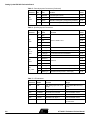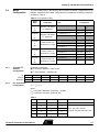
1
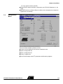
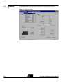
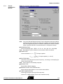
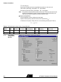
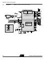
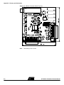
AT76C651 Evaluation Kit
USER MANUAL
Table of Contents
Section 1
Introduction ........................................................................................... 1-1
1.1
1.2
1.3
Scope........................................................................................................1-1
Deliverables ..............................................................................................1-1
System Requirements...............................................................................1-1
Section 2
Setting Up the EBC651 Evaluation Board ............................................ 2-1
2.1
2.2
2.3
2.4
Board Functionality ...................................................................................2-1
Board Interfaces........................................................................................2-1
EBC651 Board and Layout .......................................................................2-1
External Access ........................................................................................2-2
2.4.1
Power Supply .....................................................................................2-2
2.4.2
RF Input..............................................................................................2-2
2.4.3
PC Control Data .................................................................................2-2
2.4.4
MPEG2 Data Output...........................................................................2-3
2.4.5
Timing Waveforms..............................................................................2-5
2.5
2.6
Test ...........................................................................................................2-5
Board Configuration ..................................................................................2-7
2.6.1
AT76C651 I2C Address Configuration................................................2-7
2.6.2
PLL Control Bits Configuration ...........................................................2-7
Section 3
Software Installation ............................................................................. 3-1
3.1
3.2
3.3
Main Window ............................................................................................3-2
Configuration Menu...................................................................................3-3
Parameters Menu .....................................................................................3-4
3.3.1
General Configuration Window...........................................................3-5
3.3.2
Output Mode Configuration Window...................................................3-6
3.3.3
AGC1 Control Window .......................................................................3-8
3.3.4
Timing Recovery Configuration Window ............................................3-9
i
Table of Contents
3.3.5
Carrier Recovery Configuration Window ..........................................3-10
3.3.6
AGC2 Configuration Window............................................................3-10
3.3.7
Equalizer Window.............................................................................3-11
3.3.8
Forward Error Correction Window ....................................................3-12
3.3.9
PID Filtering Window ........................................................................3-13
3.4
View Menu ..............................................................................................3-13
Section 4
Appendix - Glossary and Schematics................................................... 4-1
4.1
4.2
ii
Abbreviations ............................................................................................4-1
Schematics ...............................................................................................4-2
Section 1
Introduction
1.1
Scope
The AT76C651 Evaluation Kit is designed to show the performance of the AT76C651
DVB/DAVIC QAM Demodulator and to give an example of its implementation. The principal application is the digital demodulation of QAM signals used for digital TV over
cable networks. The AT76C651 device can also be used in a number of other applications, e.g. MMDS, radio transmission, satellite transmission.
This manual is structured as follows:
1. Section 1 provides an overview.
2. Section 2 contains set-up information for the evaluation board.
3. Section 3 describes the software installation.
4. An appendix contains a glossary and schematics of the device and board.
1.2
1.3
Deliverables
System
Requirements
The AT76C651 Evaluation Kit contains:
■ An Atmel evaluation board EBC651 containing the AT76C651 circuit
■
Microsoft Windows® 95/98-compatible software on CD-ROM to configure and monitor
the AT76C651 device. The CD-ROM contains all documentation for the AT76C651
device and the EBC651 evaluation board.
■
A cable to connect the evaluation board between the PC CONTROL Connector to a
PC parallel port
The pre-requisites for use of the AT76C651 Evaluation Kit are:
■ Three DC power supplies
■
A QAM signal source (e.g. QAM modulator, Digital CATV Network, etc.)
■
A PC with:
- Windows 95/98 installed (Windows NT® is not supported)
- A CD-ROM drive(to install software)
- An SVGA display
- An available parallel port (LPT1 or LPT2)
AT76C651 Evaluation Kit User Manual
1-1
Introduction
AT76C651 Evaluation Kit User Manual
1-2
Section 2
Setting Up the EBC651 Evaluation
Board
2.1
Board
Functionality
The RF input signal is downconverted to an IF signal by a tuner integrating an AGC.
The analog signal goes through a SAW filter to attenuate adjacent channels.
A fixed-gain amplifier is used to compensate the SAW filter attenuation.
The analog signal is sent to the AT76C651 device via an external 10-bit analog-to-digital
converter to be processed (see AT76C651 datasheet, Literature Number 1293).
At the output, the digital MPEG2 frame and synchronization signals are available.
2.2
Board Interfaces
The EBC651 evaluation board consists of three interfaces:
■ CATV Tuner: Analog input ready to receive UHF - VHF frequencies in compliance with
European or US regulations.
■
MPEG2 Data: MPEG2 frame and several synchronization signals are available:
- to be sent to an MPEG2 device (e.g. Demux, Decoder, etc.)
- to effect measurement (bit error rate, channel distortion, constellation, ...)
■
2
I C Interface: Controlled by a PC parallel port, used to configure the AT76C651
demodulator and the DAT702X tuner
Note:
2.3
EBC651 Board
and Layout
It is possible to observe some signals to evaluate the transmission quality and
other information by using test connectors and LEDs.
Storage temperature: -25°C to +75°C
Operating Temperature: 0°C to +55°C
Board dimensions: 100 x 100 mm (without connectors) - Height: 50 mm
ESD protection: The PCB is not sensitive if standard EMC rules are followed.
PCB Design: Is provided as a reference design for Atmel customers.
AT76C651 Evaluation Kit User Manual
2-1
Setting Up the EBC651 Evaluation Board
2.4
External Access
2.4.1
Power Supply
Three power supplies are required:
Table 1. Power Supply Requirements
Name
VCC
Voltage
Current
Devices
96 mA max
Tuner
20 mA max
PC Buffers
40 mA max
MPEG2-DATA Buffers
600 mA max
+3.3V AT76C651
63 mA max
+3.3V External ADC (if used)
80 mA max
LEDs
+5V ± 5%
Total
VEE
VGG
2.4.2
RF Input
900 mA max
1.5 mA max
Op Amplifier (if used)
20 mA max
IF Amplifier
+12V ± 5%
Total
22 mA max
+32V ± 1V
1.5 mA max
Tuner Varicap (very sensitive)
Table 2. RF Input
Tuner Type
Characteristics
2.4.3
PC Control Data
DAT7021
(European Version)
DAT7025
(US Version)
Input Impedance
75Ω ± 5Ω unbalanced
75Ω ± 5Ω unbalanced
Input Frequency Range (RF)
48.25 MHz to 863.25 MHz
55.25 MHz to 801.25 MHz
Band Width
8 MHz
6 MHz
Connector Type
RCA Jack
Type F (3/8 UNEF 2A)
Level Input (Range for Digital
Signals)
-61 dBm to -41 dBm
-63 dBm to -37 dBm
Output Frequency (IF)
36 MHz
44 MHz
Connector Type
Mechanical: female SUB-D 25 pins
PCB Reference: J6 - PC CONTROL
DC Characteristics
Technology: 74LS05 (Low Shottky)
Output low level current: 8 mA max (open collector)
High Level Input Voltage: 2.00V min
Low Level Input Voltage: 0.80V max
Low Level Output Voltage: 0.50V max (8 mA load)
High Level Output Voltage: VCC supply on board (+5.50V max)
AC Characteristics
Frequency Input: 10 MHz max
2-2
AT76C651 Evaluation Kit User Manual
Setting Up the EBC651 Evaluation Board
Table 3. Connection Table
Pin
MPEG2 Data Output
Description
1
No Connect
2
PC_CTRL0
Bit 0 for AT76C651 PLL Control
3
PC_CTRL1
Bit 1 for AT76C651 PLL Control
4
No Connect
5
RESET_PC
6
No Connect
7
No Connect
8
No Connect
9
No Connect
10
No Connect
11
SDA_IN
12
No Connect
13
No Connect
14
SDA_OUT
15
No Connect
16
No Connect
17
SCL_OUT
18
GND
19
GND
20
GND
21
GND
22
GND
23
GND
24
GND
25
GND
Notes:
2.4.4
Signal Name(1)
Hardware Reset
I2C data from AT76C651 to PC(2)
I2C data from PC to AT76C651(2)
I2C clock from PC to AT76C651(2)
1. All signals are inverted by buffers 74LS05 mounted on the board.
2. These signals are also inverted by the PC parallel port.
Connector Type
Mechanical: female SUB-D 25 pins
PCB Reference: J7 - DATA OUTPUT
DC Characteristics
Technology: 74HCT541 (high-speed CMOS, TTL logic)
Output Max Current: 20 mA
Low-Level Output Voltage: 0.33V max (6 mA load)
High-Level Output Voltage: 4.00V min (6 mA load), 5.00V Max
AT76C651 Evaluation Kit User Manual
2-3
Setting Up the EBC651 Evaluation Board
Table 4. Connection Table
Pin
2-4
Signal Name
Description
1
CORBYTE
Corrected Byte Indicator
2
FVALID
Valid MPEG2-TS Frame
3
FSTART
Start of MPEG2-TS Frame
4
DVALID
Byte Clock - MPEG2-TS Byte Output Enable
5
D0
LSB
6
D1
7
D2
8
D3
9
D4
10
D5
11
D6
12
D7
MSB
13
CORFAIL
RS Packet Not Corrected
14
GND
15
GND
16
GND
17
GND
18
GND
19
GND
20
GND
21
GND
22
GND
23
GND
24
GND
25
GND
DATAOUT: MPEG2-TS Parallel Byte
AT76C651 Evaluation Kit User Manual
Setting Up the EBC651 Evaluation Board
2.4.5
Timing Waveforms
25 ns
DVALID
FSW
D(0..7)
FSTART
FVALID
188 bytes
16 bytes
2.5
Test
Table 5. General-purpose Connectors
Reference
TP2
FLAG
TP5
I 2C
TP7
MPEG2
DATA
AT76C651 Evaluation Kit User Manual
Signal
Name
Function
Level
1
IRQ
Interrupt Request Generated by AT76C651
3.3V
2
PID0
PID Filtering Indicator Bit 0
3.3V
3
PID1
PID Filtering Indicator Bit 1
3.3V
4
CLKO
Auxiliary Clock (for tuner or other specific usage)
3.3V
1
T_SDA
I2C Bus Data Line SDA between Tuner and
AT76C651 (bi-directional)
5.0V
2
T_SCL
I2C Bus Clock SCL from AT76C651 to Tuner
5.0V
3
SDA
SDA Line of I2C Bus (bi-directional)
5.0V
Pin
2
4
SCL
SCL line of I C Bus
5
GND
GND
1
GND
GND
2
FVALID
FRAMVALID: Valid MPEG2-TS Frame (in // mode)
3.3V
3
FSTART
FRAMSTART: Start of MPEG2-TS Frame
3.3V
4
DVALID
DATAVALID: MPEG2-TS Byte Output Enable
(active low)
3.3V
5
D7
MSB
6
D6
7
D5
8
D4
9
D3
10
D2
11
D1
12
D0
DATAOUT: MPEG2-TS Parallel Byte
5.0V
3.3V
LSB
2-5
Setting Up the EBC651 Evaluation Board
Table 5. General-purpose Connectors (Continued)
Reference
TP8
FAULT
Signal
Name
Function
Level
1
CORBYTE
Corrected Byte Indicator
3.3V
2
CORFAIL
RS Packet Not Corrected
3.3V
3
LOCK2
Maskable Lock Signal 2 (configured by software)
3.3V
4
LOCK1
Maskable Lock Signal 1 (configured by software)
3.3V
Pin
Table 6. Specific-purpose Connectors
Reference
TP1
JTAG
TP3
PC I2C
TEST
TP4
TEST
TP6
PC_CTRL
Pin
Signal
Name
Function
Level
1
TDO
3.3V
2
TRST
3.3V
3
TCK
4
TMS
5
TDI
3.3V
JTAG i.e. IEEE 1149.1
3.3V
3.3V
2
1
-> SDA_N
I C DATA from AT76C651 to PC
5.0V
2
<- SDA_N
I2C DATA from PC to AT76C651
5.0V
3
<- SCL_N
I2C CLOCK from PC to AT76C651
5.0V
4
GND
GND
1
REF2CLK
2
PHASYM
3
ENSYM
1
CTRL0_ PC
Bit 0 for AT76C651 PLL Control (inverted)
5.0V
2
CTRL1_ PC
Bit 1 for AT76C651 PLL Control (inverted)
5.0V
3
RESET_PC
Hardware Reset (inverted - active high )
5.0V
0V
3.3V
Test Pins
3.3V
3.3V
Table 7. LED Indicators
2-6
Reference
PCB
Name
CR1
Function
Origin
OR
ADC Analog Input level Out of
Range
From AD9051BRS Device (if
used)
CR2
CORBYTE
Corrected Byte Indicator
From AT76C651 Device
CR3
CORFAIL
RS Packet not Corrected
From AT76C651 Device
CR4
LOCK2
Maskable Lock Signal 2
From AT76C651 Device
CR5
LOCK1
Maskable Lock Signal 1
From AT76C651 Device
CR6
RESET
Reset of the AT76C651 Device
Push Button or Software via
PC Connector
AT76C651 Evaluation Kit User Manual
Setting Up the EBC651 Evaluation Board
2.6
Board
Configuration
The cells shaded gray in the following table indicate the default configuration on the
EBC651 evaluation board. Other configurations are available by modifying resistances
as shown in Table 8.
Table 8. Pin Description Table
Signal
Name
Designation
I2CADDR
0
(A)
Logic
Selection of AT76C651
I2C address bit 0
AT76C651 I2C
Address
Configuration
Bit
2.6.2
I C address bit 0 = 1
R48 = 0Ω
R50 =
NC(1)
I2C address bit 0 = 0
R48 = NC
R50 = 0Ω
I C address bit 1 = 1
R34 = 0Ω
R49 = NC
I2C address bit 1 = 0
R34 = NC
R49 = 0Ω
Selection by PC CONTROL
R10 = 0Ω
PLLCTRL0 = 0
R10 = NC
R37 = 0Ω
PLLCTRL0 = 1
R10 = NC
R37 = NC
Selection by PC CONTROL
R11 = 0Ω
PLLCTRL1 = 0
R11= NC
R38 = 0Ω
PLLCTRL1 = 1
R11= NC
R38 = NC
PLLCTRL2 = 0
R6 = 0Ω
R27 = NC
PLLCTRL2 = 1
R6 = NC
R27 = 0Ω
2
I2CADDR
1
(A)
Selection of AT76C651
I2C address bit 1
PLLCTRL
0
(B)
Selection of bit 0 for
AT76C651 PLL control
PLLCTRL
1
(B)
Selection of bit 1 for
AT76C651 PLL control
PLLCTRL
Selection of bit 2 for
2
AT76C651 PLL control
(B)
Note:
1. NC = No Connect
2.6.1
Configuration
2
By default on the board
2
■ I C AT76C651 address = 0001101 bin
■
I2C Tuner address = 11000010 bin
MSB
LSB
Contents
0
0
0
1
1
I2CADDR1
I2CADDR0
-
Read/write
-
-
-
-
-
-
-
R/W
PLL Control Bits
Configuration
n
F ref = --- × F xtal
2
where:
Fref = AT76C651 Reference Frequency ≤ 80 MHz
Fxtal = Oscillator Frequency (Quartz or XO)
Table 9.
n
PLLCTRL2
PLLCTRL1
PLLCTRL0
2
1
0
0
4
0
0
0
5
0
0
1
6
0
1
0
7
Note:
AT76C651 Evaluation Kit User Manual
Note
Bypass the PLL
When using XTAL oscillator
by default, PC drives PLLCTRL1 & 0
0
1
1
Results of other configurations cannot be assured.
2-7
Setting Up the EBC651 Evaluation Board
2-8
AT76C651 Evaluation Kit User Manual
Section 3
Software Installation
The AT76C651 Evaluation Kit software is provided for performance evaluation of the
AT76C651 circuit.
The software simplifies the configuration and transmission monitoring. By default, the
software is configured to be used with this evaluation board in DVB mode, however it is
possible to configure some parameters to effect specific test and measurement
operations.
To install the software, execute SETUP.EXE and follow the instructions given. When the
software starts, the PC printer ports are scanned to find a powered evaluation board. If
no board is found, a special DEMO MODE is enabled. In this mode the software can be
tested without the evaluation board.
Note: To prevent damage on your PC printer port, connect the board only when the
PC is turned off. The following screen images can differ slightly depending on
user software version.
AT76C651 Evaluation Kit User Manual
3-1
Software Installation
3.1
Main Window
Figure 3-1. Main Window
■
MONITORING indicates data registers read on chip:
BER1: Indicates a BER estimate over the last 10E8 bits
BER2: Indicates an alternate BER estimate (only informative for highly degraded
signal)
NPERR: Indicates the number of uncorrected frames on the last 108 bits
AGC1: Output level for AGC pin, value in percent between max. and min. AGC
values
AGC2: Value of AGC2 indicated in dB
Timing Offset: Offset on Symbol Rate recovered
Frequency Offset: Offset on Intermediate Frequency recovered
C/N: Carrier to Noise Ratio estimation
Phase Noise: Indicates Phase Noise in dBc integrated in the signal BandWidth
Indicates estimated Phase Noise at 10 kHz offset from the carrier
XXX Lock: A point appears when signal is activated
I/Q Inverted: Indicates whether or not I and Q channels are inverted
■
GENERAL CONFIGURATION indicates configuration of main registers:
Modulation Type
Symbol Rate
DDS Downconverting Frequency
Coherent Modulation (Visible only if QPSK modulation is selected)
■
TUNER - RF indicates tuner data registers
RF Frequency (Input)
3-2
AT76C651 Evaluation Kit User Manual
Software Installation
I2C Tuner switch activation (On/Off)
3.2
Configuration
Menu
■
SETAUTOCFG enables automatic configuration (see AT76C651 Datasheet, Lit. No.
1293).
■
RESTART performs a Software Reset to initialize device datapath (the configuration
registers are not modified).
Figure 3-2. Configuration Menu
This menu allows standard operations on files:
■ Creates a new configuration and executes a hardware reset.
■
Opens a configuration file.
■
Saves a configuration file.
■
Prints I2C registers list.
■
Print Preview displays saved I2C parameters and Monitoring registers.
AT76C651 Evaluation Kit User Manual
3-3
Software Installation
3.3
Parameters
Menu
The Parameters Menu opens a series of windows for configuring the AT76C651.
Figure 3-3. Parameters Menu
3-4
AT76C651 Evaluation Kit User Manual
Software Installation
3.3.1
General
Configuration
Window
Figure 3-4. General Configuration Window
Note:
■
If one of the General Registers (except Tuner Configuration) has been modified,
a SetAutoCfg must be carried out so that other registers are reconfigured coherently. Some registers may then be modified to match specific needs. A software
restart in the Main Window is recommended after a configuration change.
QAM MODULATION
Select demodulation type : QPSK - 16 - 32 - 64 - 128 - 256 - 512 - 1024 QAM.
Note: Demodulation Type is indicated in main window if QPSK is selected.
■ SYMBOL RATE
F ref
Indicate in Mbaud D symbol ≤ --------- if 32-taps equalizer.
8
F xtal
D symbol ≤ ---------------------- if 16-taps equalizer (α = roll-off).
2( 1 + α )
■ DDS FREQUENCY
Indicate the internal Downconverted Frequency, according to subsampling frequency used by the ADC.
Note: Correct value is automatically computed.
■ MAPPING TYPE
Select DVB or DAVIC mapping.
■
DEMODULATION TYPE FOR QPSK ONLY
■
TUNER CONFIGURATION
Select coherent demodulation or non-coherent demodulation.
Indicate RF Frequency Input (62.50 kHz step size).
Indicate I2C TUNER address (Fixed on this evaluation board).
AT76C651 Evaluation Kit User Manual
3-5
Software Installation
I2C Tuner On [on]
Select type of board and tuner recognizable by a sticker on the tuner unit:
USA version (DAT7025): 48.25 MHz ≤ RF ≤ 863.25 MHz
European version (DAT7021): 55.25 MHz ≤ RF ≤ 801.25 MHz
It is generally recommended to switch off the tuner I2C bus as soon as the tuner
frequency is configured in order to reduce the phase noise introduced by the
tuner (see AT76C651 datasheet, Literature Number 1293).
BOARD PARAMETERS
Note:
■
Indicate parameter values configured on the board:
Quartz or XO frequency: Enter the value of the component (Fxtal)
IC Reference Frequency: Enter value of n in the following formula (see Table 9)
n
F ref = --- × F xtal
2
Table 9. DVB Application using a Quartz: 32-taps Equalizer
Board
BW
IF Tuner
Fxtal = Fsampl
DDS Frequency
USA
6 MHz
44 MHz
25 MHz
2x25 - 44 = 6 MHz
EUROPE
8 MHz
36 MHz
28.9 MHz
36 - 28.9 = 7.1 MHz
3.3.2
3-6
Output Mode
Configuration
Window
Reference
Frequency
Dsymbol max
n=4
2x25 = 50 MHz
50/8 = 6.25 Mbaud
n=4
2x28.9 = 57.8 MHz
57.8/8 = 7.225 Mbaud
n
Figure 3-5. Output Mode Configuration Window
AT76C651 Evaluation Kit User Manual
Software Installation
This window allows the configuration of AT76C651 output pin:
■ OUTPUT MODE
Select format and type of the Data Output.
■
LOCK 1 and LOCK 2 MASK
Select one or more lock signals for MASKLOCK output pin:
FEC : Forward Error Correction
Carrier Recovery
Equalizer Recovery
Timing Recovery: Symbol Rate Recovery
AGC2
AGC1
PLL
■
TUNCLK
Enable the TUNCLK output (also called CLKO on TP2 pin 4) with the selected rate
of Fxtal (Oscillator Frequency).
■
IRQ POLARITY
Select the activation level for IRQ output (tri-state when released).
■
IRQ MASK
Select the event which activates the IRQ:
Unlock 1: IRQ activated when LOCK 1 signal goes low
Lock 1: IRQ activated when LOCK 1 signal goes high
Unlock 2: IRQ activated when LOCK 2 signal goes low
Lock 2: IRQ activated when LOCK 2 signal goes high
Signal Input Loss: IRQ activated when there is no input signal to AT76C651
Frame Lost: IRQ activated when a frame is uncorrected by the RS Decoder
Periodic Interruptions: Generate a periodic interruption with the selected period.
( Periodic_Interruptions ) × 204 × 8
T = -----------------------------------------------------------------------------------------D symbol × ( Nbits ⁄ Symbol )
Example:
Periodic interruptions
2048 frames
16384 frames
100 million bits
T (Dsymbol = 6 Mbaud, 64 QAM)
0.09 s
0.74 s
2.77 s
AT76C651 Evaluation Kit User Manual
3-7
Software Installation
3.3.3
AGC1 Control
Window
Figure 3-6. AGC1 Control Window
This dialog window allows the configuration of the external Analog AGC (AGC1) and
PWM output:
■ External AGC
Minimum Value: Define the minimum limit of the AGC1 Output Level (1V for this
tuner, so 51 dec).
Maximum Value: Define the maximum limit of the AGC1 Output Level (3V for this
tuner, so 153 dec).
Freeze AGC1: Freeze the current value of AGC1.
■
Baseband conversion configuration:
Disable DC Offset Compensation: Disable the DC Offset correction.
Amplifier with negative slope: Change sign of slope for AGC Output (positive for this
TUNER) Slope negative: Activated when the control voltage increases and the
amplifier gain decreases.
■
Constant PWM Output
Define CSTPWM Level Output if used (optional).
3-8
AT76C651 Evaluation Kit User Manual
Software Installation
3.3.4
Timing Recovery
Configuration
Window
Figure 3-7. Timing Recovery Configuration Window
This window allows the configuration of Timing Recovery Parameters.
These parameters are automatically configured by the SetAutoCfg button in the Main
Window.
AT76C651 Evaluation Kit User Manual
3-9
Software Installation
3.3.5
Carrier Recovery
Configuration
Window
Figure 3-8. Carrier Recovery Configuration Window
This window allows the configuration of Carrier Recovery Parameters.
These parameters are automatically configured by the SetAutoCfg button in the Main
Window.
3.3.6
AGC2 Configuration
Window
Figure 3-9. AGC2 Configuration Window
This window allows the configuration of AGC2 parameters.
These parameters are automatically configured by the SetAutoCfg button in the Main
Window.
3-10
AT76C651 Evaluation Kit User Manual
Software Installation
3.3.7
Equalizer Window
Figure 3-10. Equalizer Window
■
Equalizer Inhibition
■
Freeze Equalizer
Make the Equalizer transparent.
Freeze the coefficients in the Equalizer Filter.
■
Equalizer 16-taps only
Select 16-taps equalizer (enable Symbol Rate < FREF/4 ) else equalizer will have 32
taps.
■
Equalizer Structure
LE: Linear Equalizer (mandatory if 16-taps equalizer is chosen)
DFE: Decision Feedback Equalizer with central tap between 0..7 or 8..15
■
Central Tap Adaptation Mode
This parameter enables (or inhibits) the adaptation of the equalizer central tap. It
controls both the real part and the imaginary part.
■
Equalizer Adaptation Step
The adaptation speed of the equalizer is proportional to this parameter. A small
value slows the adaptation of the equalizer taps and reduces the noise influence on
the equalizer transfer function.
■
Central Tap Position
0..15 for 16-taps LE structure
0..31 for 32-taps LE structure
0..7 or 8..15 for DFE structure
AT76C651 Evaluation Kit User Manual
3-11
Software Installation
3.3.8
Forward Error
Correction Window
Figure 3-11. Forward Error Correction Window
This window allows the configuration of FEC Parameters.
These parameters are automatically configured by the SetAutoCfg button in the Main
Window.
■ I/Q Manual Inversion
Select manual inversion, otherwise the setting is automatic.
■
Frame Length
Length of frame (L = I x M Deinterleaver).
■
Frame Synchronization Word
First byte of MPEG2 Frame.
■
Deinterleaver Branch Number (I)
Deinterleaver configuration.
■
Deinterleaver Memory Step (M)
■
FEC Inhibitions
Deinterleaver configuration.
Disable the specified functions.
3-12
AT76C651 Evaluation Kit User Manual
Software Installation
3.3.9
PID Filtering
Window
Figure 3-12. PID Filtering Window
This menu specifies the PID of MPEG frames which must be flagged by FLAGPID0 &
FLAGPIDG1 pin output.
PID values can be configured only if the filter is on (PID1/PID2) and the mask is not null
(PID3).
3.4
View Menu
Figure 3-13. View Menu
This menu enables the user to configure the screen display, and view the QAM constellation and equalizer.
■ STATUS BAR
Enable/Disable the status bar at the bottom of the Main Window.
■
MONITORING On/Off
Enable/Disable the automatic update of monitoring information.
AT76C651 Evaluation Kit User Manual
3-13
Software Installation
■
CONSTELLATION DISPLAY
Opens a window displaying the QAM constellation
Note:
As data are collected by a slow I2C interface, all points cannot be displayed. In
Demo Mode, all points are random data.
The cursor allows the user to choose the zoom level (no effect on the device).
3-14
AT76C651 Evaluation Kit User Manual
Software Installation
■
EQUALIZER DISPLAY
Opens a window monitoring the equalizer, coefficients and the spectrum
compensation.
AT76C651 Evaluation Kit User Manual
3-15
Software Installation
3-16
AT76C651 Evaluation Kit User Manual
Section 4
Appendix - Glossary and Schematics
4.1
Abbreviations
The following abbreviations are used in this document:
ADC
Analog to Digital Converter
AGC
Automatic Gain Control
CATV
Cable Television
DVB
Digital Video Broadcasting
EMC
Electromagnetic Compatibility
ESD
Electromagnetic Discharge
ETS
European Telecommunication Standards
FEC
Forward Error Correction
IF
Intermediate Frequency
2
IC
Standard I2C bus described by “The I2C bus and how to use it - Philips
Semiconductor - April 1995”
IRQ
Interrupt Request
ITU -T
International Transmission Union - Telecommunication
MPEG
Moving Picture Expert Group
PID
Program Identifier of MPEG2 frame
PLL
Phase Locked Loop
PWM
Pulse Width Modulation
QAM
Quadrature Amplitude Modulation
QPSK
Quadrature Phase Shift Keying
RF
Radio Frequency
RS
Reed Solomon - to Correct DATA on MPEG2 frame
SAW
Surface Acoustic Wave (filters type)
TS
Transport Stream
XO
Crystal Oscillator unit
XTAL
Crystal unit
AT76C651 Evaluation Kit User Manual
4-1
Appendix - Glossary and Schematics
Schematics
Figure 4-1. EBC651 Evaluation Board Schematic
TP1 - JTAG
0
TP2
TP4 - TEST
REF2CLK
ENSYM
PHASYM
IRQ
FLAGPID0
TCK
TDO
TDI
TMS
TRST
IEEE 1149.1
JTAG PINOUT
LOCK1
LOCK2
J7 - SUB-D 25 pts
MPEG2 FRAME - I&Q DATA
SMPLPHASE
R7
TUNCLK
TP8
R13
VDD
FLAGPID1
4.2
1
CORFAIL
TEST OUTPUTS
CORBYTE
TUNER CATV
RF Input
SAW
Filter
OR
IF1
10
Amp
D[9..0]
VGG
FRMVALID
ADCLK
TP5
VCC
TP3
AGC Amp
SCL
SDA
CLK
1
FMRSTART
TP7
AGC
DATAVALID
AINB
IF2
VCC
AT76C651
QAM DEMODULATOR
ADC
AIN
DATAOUT[7..0]
10k
1
R60
R14
1
I2C SDA
TI2C SDA
J6 - SUB-D 25 pts
PC Parallel Port
R61
R15
TI2C SCL
1
I2C SCL
R37
AGC
R10
AT76C651 POWER CONNECTIONS
R63
TESTADC
R66
(1=ADC ext ; 0 = test)
QBB1
VDD_EXT
R67
(+3.3V - external)
QBB0
VDD3 = +3.3V
I2CVDD
VDD5 = +5.0V
PLLCTRL1
PLLCTRL2
R27
R50
LFTPLL
(0=XTAL ; 1=XO)
VEE (+12V)
RESET*
OSCMODE
VGG (+35V)
1
I2CADDR1
XTAL_I
+35V
+12V
PC reset
R48
R49
CSTPWM
XTAL_O
VDD5 (+5V )
I2CADDR0
Optional
AGC Amp
XOCLK
VDD3
(+3.3V - digit)
PC reset
GND = Ground Power
R64
Reg
1
R38
R6
GND
VDD
+5V
1
R11
TP6
R65
Reg
TEST SWITCH
R68
BOARD POWER CONFIGURATION
VDD
PLLCTRL0
R34
R33
TEST MODE
R51
PLL RC Filter
R28
VDD
VDD
XO
XTAL
R9
(VDD_EXT)
4-2
AT76C651 Evaluation Kit User Manual
Appendix - Glossary and Schematics
Figure 4-2. EBC651 Evaluation Board Top View
Note:
4-3
This drawing is not to scale.
AT76C651 Evaluation Kit User Manual
Appendix - Glossary and Schematics
Figure 4-3. EBC651 Evaluation Board Bottom View
Note:
4-4
This drawing is not to scale.
AT76C651 Evaluation Kit User Manual
Appendix - Glossary and Schematics
Figure 4-14. EBC651 Evaluation Board Connection
QAM MODULATOR
or
CATV NETWORK OUTPUT
GND
+5V
+12V
+32V
POWER SUPPLY
CATV NETWORK
TUNER
651
76C
AT
PC CONTROL
EBC651AA01
TA
DA
2
EG
UT
MP
TP
OU
DVB/DAVIC
QAM DEMODULATOR
AT76C651 Evaluation Kit User Manual
4-5
Appendix - Glossary and Schematics
Document Details
Title:
Literature Number:
Date:
AT76C651 Evaluation Kit User Manual
1320A
October 1999
Revision History
Revision A:
October 1999
Important Notice
Because the program is licensed free of charge, there is no warranty for the program, to
the extent permitted by applicable law. Except when otherwise stated in writing the
copyright holders and/or other parties provide the program “as is” without warranty of
any kind, either expressed or implied, including, but not limited to, the implied warranties
of merchantability and fitness for a particular purpose. The entire risk as to the quality
and performance of the program is with you. Should the program prove defective, you
assume the cost of all necessary servicing, repair or correction.
In no event unless required by applicable law or agreed to in writing will any copyright
holder, or any other party who may modify and/or redistribute the program as permitted
above, be liable to you for damages, including any general, special, incidental or consequential damages arising out of the use or inability to use the program (including but not
limited to loss of data or data being rendered inaccurate or losses sustained by you or
third parties or a failure of the program to operate with any other programs), even if such
holder or other party has been advised of the possibility of such damages.
Due to software upgrades, slight differences may exist between the version described in
this manual and the version delivered to customer.
This design can vary slightly depending on the version of the board used.
The user must assume the entire risk of using this evaluation kit.
For all questions regarding the information in this document, please contact:
Atmel Corporation
Digital TV Development Center
Orlytech Bat. 526
2 allée Maryse Bastié
91781 Wissous Cedex
France
Tel.: (+33) (0)1 70 03 30 05
Fax (+33) (0)1 70 03 30 13
e-mail address: [email protected]
4-6
AT76C651 Evaluation Kit User Manual
Atmel Headquarters
Atmel Operations
Corporate Headquarters
Atmel Colorado Springs
2325 Orchard Parkway
San Jose, CA 95131
TEL (408) 441-0311
FAX (408) 487-2600
Europe
1150 E. Cheyenne Mtn. Blvd.
Colorado Springs, CO 80906
TEL (719) 576-3300
FAX (719) 540-1759
Atmel Rousset
Atmel U.K., Ltd.
Coliseum Business Centre
Riverside Way
Camberley, Surrey GU15 3YL
England
TEL (44) 1276-686677
FAX (44) 1276-686697
Zone Industrielle
13106 Rousset Cedex, France
TEL (33) 4 42 53 60 00
FAX (33) 4 42 53 60 01
Asia
Atmel Asia, Ltd.
Room 1219
Chinachem Golden Plaza
77 Mody Road
Tsimshatsui East
Kowloon, Hong Kong
TEL (852) 27219778
FAX (852) 27221369
Japan
Atmel Japan K.K.
Tonetsu Shinkawa Bldg., 9F
1-24-8 Shinkawa
Chuo-ku, Tokyo 104-0033
Japan
TEL (81) 3-3523-3551
FAX (81) 3-3523-7581
Fax-on-Demand
North America:
1-(800) 292-8635
International:
1-(408) 441-0732
e-mail
[email protected]
Web Site
http://www.atmel.com
BBS
1-(408) 436-4309
© Atmel Corporation 1999.
Atmel Corporation makes no warranty for the use of its products, other than those expressly contained in the Company’s standard warranty which is detailed in Atmel’s Terms and Conditions located on the Company’s web site. The Company assumes no responsibility for
any errors which may appear in this document, reserves the right to change devices or specifications detailed herein at any time without
notice, and does not make any commitment to update the information contained herein. No licenses to patents or other intellectual property of Atmel are granted by the Company in connection with the sale of Atmel products, expressly or by implication. Atmel’s products are
not authorized for use as critical components in life suppor t devices or systems.
Marks bearing
®
and/or
™
are registered trademarks and trademarks of Atmel Corporation.
Terms and product names in this document may be trademarks of others.
Printed on recycled paper.
1320A–10/99/0M