1
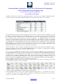
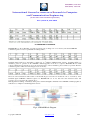
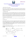
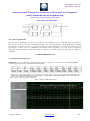
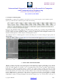
ISSN(Online): 2320-9801
ISSN (Print): 2320-9798
International Journal of Innovative Research in Computer
and Communication Engineering
(An ISO 3297: 2007 Certified Organization)
Vol. 2, Issue 6, June 2014
Design and Verification of High Speed SDRAM
Controller with Adaptive Bank Management
and Command Pipeline
Ganesh Mottee, P.Shalini
Mtech student, Dept of ECE, SIR MVIT Bangalore, VTU university, Karnataka, India.
Assistant Professor, Dept of ECE, SIR MVIT Bangalore, VTU university, Karnataka, India .
ABSTRACT: As the performance gap between microprocessors and memory continues to increase,main memory
accesses result in long latencies which become a factor limiting system performance. Previous studies show that main
memory access streams contain significant Localities and SDRAM devices provide parallelism through multiple banks
and channels.These locality and parallelism have not been exploited thoroughly by conventional memory controllers. In
this thesis, SDRAM address mapping techniques and memory access reordering mechanisms are studied and applied to
memory controller design with the goal of reducing observed main memory access latency. The application of the
synchronous dynamic random access memory (SDRAM) has gone beyond the scope of personal computers for quite a
long time. It comes into hand whenever a big amount of low price and still high speed memory is needed. Most of the
newly developed stand alone embedded devices in the field of image, video and sound processing take more and more
use of it. The big amount of low price memory has its trade off – the speed. In order to take use of the full potential of
the memory, an efficient controller is needed. Efficient stands for maximum random accesses to the memory both for
reading and writing and less area after implementation.
I. INTRODUCTION
The High-Speed SDRAM Controller offers storage extension for memory critical applications. For example with
packet-based traffic as in IP networks, storage requirements can become crucial when complete frames need to be
stored . The Controller implements a burst optimized access scheme, which offers transfer rates up to 4 Gbit/s at
125MHz. All SDRAM device specifics, like row and column multiplexing, page burst handling; page and bank
switching are completely hidden from the user application. Power-up initialization, refresh and other management tasks
necessary to provide data integrity in the SDRAM are done automatically and also hidden from the user application.
The Controller interfaces directly to SDRAM memory devices and provides a simple and easy-to-use split-port user
interface (separate read and write ports). It allows for single word accesses as well as arbitrary length bursts emulating
a linear memory space with no page or bank boundaries. The SDRAM Controller can easily be connected to other
MorethanIP solutions or us backend for large FIFO application
II. RELATED WORK
Synchronous DRAM (SDRAM) has become a mainstream memory of choice in embedded system memory design. For
high-end applications using processors the interface to the SDRAM is supported by the processor’s built-in peripheral
module. However, for other applications, the system designer must design a controller to provide proper commands for
SDRAM initialization, read/write accesses and memory refresh. This SDRAM controller reference design, located
between the SDRAM and the bus master, reduces the user’s effort to deal with the SDRAM command interface by
providing a simple generic system interface to the bus master. Figure 1 shows the relationship of the controller between
the bus master and SDRAM. The bus master can be either a microprocessor or a user’s proprietary module interface.
SDRAM is high-speed Dynamic Random Access Memory (DRAM) with a synchronous interface. The synchronous
interface and fully pipelined internal architecture of SDRAM allows extremely fast data rates if used efficiently.
SDRAM is organized in banks of memory addressed by row and column. The number of row and column address bits
depends on the size and configuration of the memorySDRAM is controlled by bus commands that are formed using
Copyright to IJIRCCE
www.ijircce.com
4802
ISSN(Online): 2320-9801
ISSN (Print): 2320-9798
International Journal of Innovative Research in Computer
and Communication Engineering
(An ISO 3297: 2007 Certified Organization)
Vol. 2, Issue 6, June 2014
combinations of the ras_n, cas_n, and we_n signals. For instance, on a clock cycle where all three signals are high, the
associated command is a No Operation (NOP). A NOP is also indicated when the chip select is not asserted.
Fig 2.1 Table of command
These banks must be opened before a range of addresses can be written to or read from. The row and bank to be opened
are registered coincident with the Active command. When a new row on a bank is accessed for a read or a write it may
be necessary to first close the bank and then re-open the bank to the new row. Closing a bank is performed using the
Prec command. Opening and closing banks costs memory bandwidth, so the SDRAM Controller Core has been
designed to monitor and manage the status of the four banks simultaneously. This enables the controller to intelligently
open and close banks only when n When the Read or Write command is issued, the initial column address is presented
to the SDRAM devices. The initial data is presented concurrent with the Write command. For the read command, the
initial data appears on the data bus 1 known as CAS latency and is due to the time required to physically read the
internal DRAM andregister the data on the bus. The CAS latency depends on the speed frequency of the memory clock.
In general, the faster the clock, the more cycles of CAS latency is required.
After the initial Read or Write command, sequential read and writes will continue until the burst length is reached or
support a burst length of up to 8 data cycles. The SDRAM Controller Core is capable of cascading bursts to maximize
SDRAM bandwidth. Fig 2.1 Table of command1-4 clock cycles later.
This is grade of the SDRAM and thea Burst Terminate command is issued. SDRAM devices command Precharge
necessary SDRAM devices require periodic refresh operations to maintain the data. The SDRAM Controller Core
automatically issues the Auto Refresh comman periodically. No user intervention is required The Load Mode Register
command is used to configure the SDRAM operation. This register stores the CAS latency, burst length, burst type, and
write burst mode. The SDR controller only writes to the base mode register Non-adaptive controller opens and closes
banks for each transaction. SDRAM command time sequence for two sequential block writing to the same bank like:
Fig 2.2 Nonadaptive controller opens and closes bank for each transactions
Consider SDRAM command sequence for block writing with closed bank a and to the row controller keeps these banks
open also. Then the sequence for non the following:
Consider SDRAM command sequence for block writing with Burst Length equal to 4 to closed bank a and to the row
1 of bank b with opened row 0. Assume, that the non-adaptive controller keeps these banks open also. Then the
sequence for non adaptive controller will be the following
Copyright to IJIRCCE
www.ijircce.com
4803
ISSN(Online): 2320-9801
ISSN (Print): 2320-9798
International Journal of Innovative Research in Computer
and Communication Engineering
(An ISO 3297: 2007 Certified Organization)
Vol. 2, Issue 6, June 2014
III. PROPOSED ALGORITHM
HSSDRC IP Core keeps all banks open and closes them only to change row or for memory refresh and SDRAM
command sequence for two sequential block writing will be :
These two write transaction will consume 11 clock ticks. It gives a benefit of 8 clock ticks or 42 % of a memory write
bandwith. This bank access algorithm is called here as “Adaptive SDRAM bank control“. Command NOP is a
mandatory pause in operation of the SDRAM command pipeline in the above sequences HSSDRC IP Core bank
control commands for next memory access are inserted in place of these mandatory pauses whenever possible. Then the
command sequence will be the following (best case is shown):
These two write transactions will consume 11 clock ticks. It gives a benefit of 8 clock tick or 42 % of a memory write
bandwith again. SDRAM command sequence for HSSDRC IP core do not have Twr time interval because this
sequence does not need it in the example above.
This algorithm for filling of mandatory NOP pauses with meaningful commands in the SDRAM command pipeline is
called here as “Adaptive command pipeline control“.
Fig 4..SDRAM Block Diagram
.
Copyright to IJIRCCE
www.ijircce.com
4804
ISSN(Online): 2320-9801
ISSN (Print): 2320-9798
International Journal of Innovative Research in Computer
and Communication Engineering
(An ISO 3297: 2007 Certified Organization)
Vol. 2, Issue 6, June 2014
4.1 Refresh window generator module
While the memory is operating, each memory cell must be refreshed repetitively, within the maximum interval between
refreshes specified by the manufacturer, which is millisecond region. Refreshing does not employ the normal memory
operations (read and write cycles) used to access data, but specialized cycles called generated by separate counter
circuits in the memory circuitry a normal memory accesses. The storage cells on a memory chip are laid out in a
rectangular array of rows and columns.
4.2 Input arbiter module
Contains round-robin arbiter for three independent SDRAM command decoders. A roundrobin token passing bus or
switch arbiter guarantees fairness (no starvation) among masters allows any unused time slot to be allocated to a master
whose round-robin turn is later but who is ready now A reliable prediction of the worst-case wait time is another
advantage of the round-robin protocol. The worst-case wait time is proportional to number of requestors minus one.
The protocol of a round-robin token passing bus or switch arbiter works as follows. In each cycle, one of the masters
(in round-robin order) has the highest priority (i.e., owns the token) for access to a shared resource. If the token-holding
master does not need the resource in this cycle, the master with the next highest priority who sends a request can be
granted the resource, and the highest priority master then passes the token to the next master in round-robin order.
4.3 SDRAM memory bank using map module
Contains memory for storage of the open bank and row indexes. This memory state is changed by SDRAM command
decoders.
4.3.1 Memory bank
A memory bank is a logical unit of storage in electronics, which is hardware dependent. In computer the memory bank
may be determined by the memory access controller along with physical organization of the hardware memory slots. In
a typical synchronous dynamic random-access memory (SDRAM) or double data rate synchronous dynamic randomaccess memory (DDR SDRAM), a bank consists of multiple rows and columns of storage units and is usually spread
out across several chips. In a single read or write operation, only one bank is accessed, therefore bits in a column or a
row, per bank, per chip = memory bus width in bits (single channel). The size of a bank is further determined by bits in
a column and a row, per chip× number of chips in a bank.
4.4 SDRAM command sequence decoders module
Contains three independent SDRAM command sequence decoders. The proper SDRAM command sequence is chosen
depending upon information from memory bank usage map.
DECODER
Fig 4.4 Decoder
Copyright to IJIRCCE
www.ijircce.com
4805
ISSN(Online): 2320-9801
ISSN (Print): 2320-9798
International Journal of Innovative Research in Computer
and Communication Engineering
(An ISO 3297: 2007 Certified Organization)
Vol. 2, Issue 6, June 2014
After the arbiter has accepted a command from the host, the command is passed onto the command generator portion of
the command module. The command module uses three shift registers to generate the appropriate timing between the
commands that are issued to SDRAM. One shift register is used to control the timing the ACTIVATE com second is
used to control the positioning of the READA or WRITEA commands; a third is used to time com- mand durations,
which allows the arbiter to determine if the last operation has been completed. The command module also performs the
multiplexing of the address to the SDRAM. The row portion of the address is multiplexed out to the SDRAM outputs
A[11:0] during the ACTIVATE(RAS) command. The column portion is then multiplexed out to the SDRAM address
outputs during a READA(CAS) or WRITEA command. The output signal OE is generated by the command module to
control tristate buffers in the last stage of the DATAIN path in the data path module.
4.5 Output arbiter module
Module contains round-robin arbiter and adaptive access to SDRAM command pipeline logic, analyzing decoded
commands and SDRAM banks state taken from access manager.
4.5.1 Round robin arbiter
Round robin arbitration is a scheduling scheme which gives to each requestor its share of using a common resource for
a limited time or data elements. The basic algorithm implies that once a requestor has been serves he would “go
around” to the end of the line and be the last to be served again. The simplest form of round robin arbiter is based on
assignment of a fixed time slot per requestor; this can be implemented using a circular counter. Alternatively, the
weighted round robin arbiter is defined to allow a specific number X of data elements per each requestor, in which case
X data elements from each requestor would be processed before moving to the next one. Round robin arbiters are
typically used for arbitration for shared resources, load balancing, queuing systems, and resource allocation. Any
application requiring a minimal fairness where none of the requestors is suffering from starvation is a valid application
for a round robin arbiter.
Fig 4.5 round robin arbiter
4.6 . SDRAM command pipeline access manager module
Contains FSMs for each memory bank. Module permits or inhibits access to given SDRAM bank. In the state idle the
main FSM accepts from the scheduler the best fitting requestor and splits the request into bank access (states: serve
bank0 – serve bank3). In case of a pending refresh the main FSM indicates the command generation unit the scheduled
refresh with the signal start refresh (state: serve refresh). The main FSM breaks the access granularity from requestor
level down to bank accesslevel.The scheduler provides the main FSM with the information about the best fitting
requestor, according to the arbitration policy. The main FSM accepts with a handshake the requestor prepares the
Copyright to IJIRCCE
www.ijircce.com
4806
ISSN(Online): 2320-9801
ISSN (Print): 2320-9798
International Journal of Innovative Research in Computer
and Communication Engineering
(An ISO 3297: 2007 Certified Organization)
Vol. 2, Issue 6, June 2014
access. Therefore, it routes the target address of the selected requestor to the address mapping unit. Furthermore, the
main FSM indicates to the command
Fig 4.6. FSM
4.7 SDRAM initialization module
Contains counter-based FSM creating necessary command chain for SDRAM initialization. The Controller has to go
through an initialization process by a sequence of command signals before the normal memory access.The memory
controller starts the memory initialization sequence when the init_start signal is asserted by the user interface. Once
asserted, the init_start signal needs to be held high until the initialization process is com-pleted. The output signal
init_done is asserted High for one clock cycle indicating that the core has com-pleted the initialization sequence and is
now ready to access the memory. The init_start signal must be deasserted as soon as init_done is sampled high at the
rising edge of sclk. If the init_start is left high at the next rising edge of sclk the memory controller takes it as another
request for initialization and starts the initialization process again. Memory initialization is required only once
immediately after the system reset. As part of Initialization the core performs write leveling for all the available ranks
and stores the write level delay values. The memory controller ensures a minimum gap of 500 μs between
em_ddr_reset_n deassertion and em_ddr_cke assertion. It is user’s responsibility to ensure minimum reset duration of
200 μs.
4.8. Logical command multiplex module
Contains simple command multiplexer for mixing outputs of output arbiter and initialization module. Because of
controller being passive during initialization routine due to internal synchronous reset of all decoders and arbiters,
multiplexing is substituted with logical OR.
4.9 Datapath module
Contains FSM for access to read/write data and SDRAM masking logic. The data flow design between the SDRAM
and the system interface is shown in figure. The datapath circuit consists of four number of 16-bit D flip flops and a
tristate buffer. Flip flop is used to shift the data. Tristate buffer is used to determine the direction of bidirectional data
bus. Tri state buffer has a control input which determines whether it is a read or write operation.
Copyright to IJIRCCE
www.ijircce.com
4807
ISSN(Online): 2320-9801
ISSN (Print): 2320-9798
International Journal of Innovative Research in Computer
and Communication Engineering
(An ISO 3297: 2007 Certified Organization)
Vol. 2, Issue 6, June 2014
Fig 4.9 Datapath
4.10. Address-path module
Once the memory initialization is done, the core waits for user commands in order to setup and/or access the memory.
The user logic needs to provide the command and address to the core along with the control signals. The com-mands
and addresses are delivered to the core using the following procedure. The memory controller core informs the user
logic that it is ready to receive a command by asserting the cmd_rdy signal for one cycle. If the core finds the
cmd_valid signal asserted by the user logic while it’s cmd_rdy is asserted, it takes the cmd input as a valid user
command.
IV. SIMULATION RESULTS
5.1.1 Adaptive bank management
HSSDRC IP Core keeps all banks open and closes them only to change row or form memory refresh and SDRAM
command sequence for two sequential block writing will be
The simulated result we got as shown below Fig .5.1
Fig 5.1 Adaptive bank management
Copyright to IJIRCCE
www.ijircce.com
4808
ISSN(Online): 2320-9801
ISSN (Print): 2320-9798
International Journal of Innovative Research in Computer
and Communication Engineering
(An ISO 3297: 2007 Certified Organization)
Vol. 2, Issue 6, June 2014
5.1.2 Adaptive Command pipeline
HSSDRC IP Core bank control commands for next memory access are inserted in place of these mandatory pauses
whenever possible. Then the command sequence will be the following
These two write transactions will consume 11 clock ticks. It gives a benefit 42 % of a memory write bandwith again.
SDRAM command sequence for HSSDRC IP core do not have Twr time interval because this sequence does not need
it in the example above.This algorithm for filling of mandatory NOP pauses with meaningful commands in the
SDRAM command pipeline is called “Adaptive command pipeline control“
The simulated result for command pipeline is shown below taking only 11 clock for writing two right operation in
different bank
Fig 5.1.2 Command pipeline
V. CONCLUSION AND FUTURE WORK
Pipeline operations can reduce access latency and provide bank and row address relationship of two adjacent
instructions in advance. Then the controller can make use of the address relationship to take a dynamic memory access
policy. It is really advisable for controller to choose a preferable memory access policy according to different address
relationship. So unlike the traditional memory controller, the pipeline memory controller can take both bank
interleaving and page hit optimization in the same memory system, which can maximize the utilization of memory data
bus and reduce memory access latency. The performance analysis of the execution time and throughput proves that this
pipeline SDRAM memory controller can reduce memory access latency and improve the throughput of SDRAM
memory greatly. Such a pipeline memory controller can be applied to the need of high throughput of processing.
Additionally an address reordering mechanism was introduced, which saves a lot of clock cycles on the price of
Copyright to IJIRCCE
www.ijircce.com
4809
ISSN(Online): 2320-9801
ISSN (Print): 2320-9798
International Journal of Innovative Research in Computer
and Communication Engineering
(An ISO 3297: 2007 Certified Organization)
Vol. 2, Issue 6, June 2014
comparatively less extra area. These observations coupled with the novel contributions of this work, can indicate where
future work in the field should be done to further improve the performance of the memory system, decreasing the
memory acess time, power and area. The constant need to boost memory performance for increasingly powerful system
processors drives the development of advanced memory technologies.
REFERENCES.
[1]
Single data Rate (SDR) SDRAM Specification, JEDEC STANDARD, JESD79E, May 2005
[2]
The Love/Hate Relationship with SDR SDRAM Controllers, Graham Allan, MOSAID,
[3]
128Mb SDR SDRAM, Device Specification, Hynix, April 2006
[4]
Altdq & altdqs Megafunction, User Guide, Altera, March 2005
[5]
PLLs in Stratix II & Stratix II GX Devices, April 2006
[6]
How to Use SDR SDRAM, User’s Manual, Document No. E0234E40, ALPIDA, September 2005
[7]
SDR SDRAM Controller Using Virtex-4 FPGA Devices, Oliver Despaux, Application Note, March 27, 2006.
[8]
SAULSBURY, ASHLEY, PONG, FONG, AND NOWATZYK, ANDREAS, Missing the Memory Wall: The Case for
Processor/MemoryIntegration. In Proceedings of the International Symposium on Computer Architecture (May 1996), pp.90101.
BIOGRAPHY
Ganesh.A.Mottee is a student of MTECH in the electronics and communication Department, College of SIR MVIT,
VTU University,Banglore, India
P.Shalini is currently Assistant Professor in the Department of Electronics and communication at Sir M Visvesvaraya
Institute of Technology, Bangalore, India.
Copyright to IJIRCCE
www.ijircce.com
4810