1
User’s Manual
HOW TO USE SDRAM
Document No. E0123N50 (Ver.5.0)
Date Published October 2002 (K) Japan
URL: http://www.elpida.com
© Elpida Memory, Inc. 2001-2002
© NEC Corporation 1998
Elpida Memory, Inc. is a joint venture DRAM company of NEC Corporation and Hitachi, Ltd.
SUMMARY OF CONTENTS
CHAPTER 1 PRODUCT OUTLINE .........................................................................................................................14
CHAPTER 2 FEATURES OF PRODUCTS.............................................................................................................23
CHAPTER 3 OPERATION AFTER POWER APPLICATION ................................................................................35
CHAPTER 4 BASIC SETTING (MODE REGISTER SETTING) ...........................................................................36
CHAPTER 5 STATUS TRANSITIONS ....................................................................................................................46
CHAPTER 6 COMMAND OPERATIONS ................................................................................................................50
CHAPTER 7 BASIC OPERATION MODE..............................................................................................................57
CHAPTER 8 DQM CONTROL OPERATION..........................................................................................................64
CHAPTER 9 CKE CONTROL OPERATION ..........................................................................................................68
CHAPTER 10 BURST OPERATION .......................................................................................................................77
CHAPTER 11 MULTIBANK OPERATION ...............................................................................................................84
CHAPTER 12 CALCULATION OF CURRENT CONSUMPTION ...........................................................................112
2
User’s Manual E0123N50
NOTES FOR CMOS DEVICES
1
PRECAUTION AGAINST ESD FOR MOS DEVICES
Exposing the MOS devices to a strong electric field can cause destruction of the gate
oxide and ultimately degrade the MOS devices operation. Steps must be taken to stop
generation of static electricity as much as possible, and quickly dissipate it, when once
it has occurred. Environmental control must be adequate. When it is dry, humidifier
should be used. It is recommended to avoid using insulators that easily build static
electricity. MOS devices must be stored and transported in an anti-static container,
static shielding bag or conductive material. All test and measurement tools including
work bench and floor should be grounded. The operator should be grounded using
wrist strap. MOS devices must not be touched with bare hands. Similar precautions
need to be taken for PW boards with semiconductor MOS devices on it.
2
HANDLING OF UNUSED INPUT PINS FOR CMOS DEVICES
No connection for CMOS devices input pins can be a cause of malfunction. If no
connection is provided to the input pins, it is possible that an internal input level may be
generated due to noise, etc., hence causing malfunction. CMOS devices behave
differently than Bipolar or NMOS devices. Input levels of CMOS devices must be fixed
high or low by using a pull-up or pull-down circuitry. Each unused pin should be connected
to VDD or GND with a resistor, if it is considered to have a possibility of being an output
pin. The unused pins must be handled in accordance with the related specifications.
3
STATUS BEFORE INITIALIZATION OF MOS DEVICES
Power-on does not necessarily define initial status of MOS devices. Production process
of MOS does not define the initial operation status of the device. Immediately after the
power source is turned ON, the MOS devices with reset function have not yet been
initialized. Hence, power-on does not guarantee output pin levels, I/O settings or
contents of registers. MOS devices are not initialized until the reset signal is received.
Reset operation must be executed immediately after power-on for MOS devices having
reset function.
CME0107
User’s Manual E0123N50
3
Intel is trademark or registered trademark of Intel Corporation or its subsidiaries in the United States and other
countries.
The mark ★ shows major revised points.
The information in this document is subject to change without notice. Before using this document, confirm that this is the latest version.
No part of this document may be copied or reproduced in any form or by any means without the prior
written consent of Elpida Memory, Inc.
Elpida Memory, Inc. does not assume any liability for infringement of any intellectual property rights
(including but not limited to patents, copyrights, and circuit layout licenses) of Elpida Memory, Inc. or
third parties by or arising from the use of the products or information listed in this document. No license,
express, implied or otherwise, is granted under any patents, copyrights or other intellectual property
rights of Elpida Memory, Inc. or others.
Descriptions of circuits, software and other related information in this document are provided for
illustrative purposes in semiconductor product operation and application examples. The incorporation of
these circuits, software and information in the design of the customer's equipment shall be done under
the full responsibility of the customer. Elpida Memory, Inc. assumes no responsibility for any losses
incurred by customers or third parties arising from the use of these circuits, software and information.
[Product applications]
Elpida Memory, Inc. makes every attempt to ensure that its products are of high quality and reliability.
However, users are instructed to contact Elpida Memory's sales office before using the product in
aerospace, aeronautics, nuclear power, combustion control, transportation, traffic, safety equipment,
medical equipment for life support, or other such application in which especially high quality and
reliability is demanded or where its failure or malfunction may directly threaten human life or cause risk
of bodily injury.
[Product usage]
Design your application so that the product is used within the ranges and conditions guaranteed by
Elpida Memory, Inc., including the maximum ratings, operating supply voltage range, heat radiation
characteristics, installation conditions and other related characteristics. Elpida Memory, Inc. bears no
responsibility for failure or damage when the product is used beyond the guaranteed ranges and
conditions. Even within the guaranteed ranges and conditions, consider normally foreseeable failure
rates or failure modes in semiconductor devices and employ systemic measures such as fail-safes, so
that the equipment incorporating Elpida Memory, Inc. products does not cause bodily injury, fire or other
consequential damage due to the operation of the Elpida Memory, Inc. product.
[Usage environment]
This product is not designed to be resistant to electromagnetic waves or radiation. This product must be
used in a non-condensing environment.
If you export the products or technology described in this document that are controlled by the Foreign
Exchange and Foreign Trade Law of Japan, you must follow the necessary procedures in accordance
with the relevant laws and regulations of Japan. Also, if you export products/technology controlled by
U.S. export control regulations, or another country's export control laws or regulations, you must follow
the necessary procedures in accordance with such laws or regulations.
If these products/technology are sold, leased, or transferred to a third party, or a third party is granted
license to use these products, that third party must be made aware that they are responsible for
compliance with the relevant laws and regulations.
M01E0107
4
User’s Manual E0123N50
INTRODUCTION
Target Readers
This manual is intended for users who wish to understand the function of SDRAM and
design application systems for them.
Purpose
This manual is intended to give users understanding of the basic function of SDRAM
and how to use them.
How to Use This Manual
It is assumed that readers of this manual should have general knowledge in the fields of
electrical engineering, logic circuits, and memory products. For details about the
functions of individual products, refer to the corresponding data sheet. Since the
operation examples that appear in this user's manual are strictly illustrative examples,
numerical values that appear are not guaranteed values. Use them only as reference
values.
(For specifications, refer to the Data Sheet of each product.)
Conventions
Note:
Footnote for items marked with Note in the text
Caution:
Information requiring particular attention
Remark:
Supplementary information
Numeric notation: Decimal ... xxxx
Related Documents
The related documents indicated in this publication may include preliminary versions.
However, preliminary versions are not marked as such.
Document Name
Synchronous DRAM User’s Manual
User’s Manual E0123N50
Document Number
E0124N
5
Organization
This manual consists of the following chapters.
EXPLANATION OF THE FEATURES OF THE SDRAM
CHAPTER 1 PRODUCT OUTLINE
EXPLANATION OF THE SYNCHRONOUS OPERATIONS AND SPECIFIC FUNCTIONS
CHAPTER 2 FEATURES OF PRODUCTS
CHAPTER 3 OPERATION AFTER POWER APPLICATION
CHAPTER 4 BASIC SETTING (MODE REGISTER SETTING)
CHAPTER 5 STATUS TRANSITIONS
CHAPTER 6 COMMAND OPERATIONS
CHAPTER 7 BASIC OPERATION MODE
CHAPTER 8 DQM CONTROL OPERATION
CHAPTER 9 CKE CONTROL OPERATION
CHAPTER 10 BURST OPERATION
CHAPTER 11 MULTIBANK OPERATION
CHAPTER 12 CALCULATION OF CURRENT CONSUMPTION
6
User’s Manual E0123N50
CONTENTS
CHAPTER 1 PRODUCT OUTLINE..........................................................................................................................14
1.1 Pin Configuration.........................................................................................................................................15
1.2 Pin Functions...............................................................................................................................................16
1.2.1 CLK input ...........................................................................................................................................16
1.2.2 CKE input ...........................................................................................................................................16
1.2.3 /CS input ..........................................................................................................................................16
1.2.4 /RAS, /CAS, /WE input.....................................................................................................................16
1.2.5 VCC, VSS ............................................................................................................................................16
1.2.6 VCCQ, VSSQ ......................................................................................................................................16
1.2.7 Address (A0 through Ax) input .........................................................................................................17
1.2.8 DQM0 through DQM3 input..............................................................................................................19
1.2.9 DQ0 through DQx I/O.......................................................................................................................19
1.3 Block Diagram .............................................................................................................................................20
1.3.1 Block diagram of 128M SDRAM (µPD45128163) ............................................................................20
1.4 Description of Block Diagram ....................................................................................................................21
1.4.1 Memory cell array of 128M SDRAM (µPD45128163).......................................................................21
1.4.2 Address (Row, Column) decoders ...................................................................................................22
1.4.3 I/O buffer ..........................................................................................................................................22
1.4.4 Refresh counter................................................................................................................................22
CHAPTER 2 FEATURES OF PRODUCTS.............................................................................................................23
2.1 Clock Synchronization Operation ..............................................................................................................24
2.2 Control by Command ..................................................................................................................................25
2.2.1 Command input timing .....................................................................................................................25
2.2.2 SDRAM command list ......................................................................................................................26
2.3 Plural Bank Configuration ..........................................................................................................................27
2.3.1 Four-bank configuration ...................................................................................................................27
2.4 Burst Transfer ..............................................................................................................................................28
2.5 Comparison with General-Purpose DRAM ................................................................................................30
2.5.1 Increasing speed of DRAM ..............................................................................................................30
2.5.2 Basic control method and access time ............................................................................................31
CHAPTER 3 OPERATION AFTER POWER APPLICATION ................................................................................35
3.1 Initialization after Power Application.........................................................................................................35
3.2 Initializing .....................................................................................................................................................35
CHAPTER 4 BASIC SETTING (MODE REGISTER SETTING) ...........................................................................36
4.1 Mode Register Setting.................................................................................................................................36
4.1.1 Setting ..............................................................................................................................................36
4.1.2 Set parameters.................................................................................................................................37
4.1.3 Setting of burst length, wrap type, and /CAS latency.......................................................................45
CHAPTER 5 STATUS TRANSITIONS ....................................................................................................................46
5.1 Status Transition Diagram ..........................................................................................................................46
5.1.1 Status transition diagram of 128M SDRAM (µPD45128163) ...........................................................47
5.2 Status Description .......................................................................................................................................48
5.2.1 Idle ...................................................................................................................................................48
User’s Manual E0123N50
7
5.2.2 Row active........................................................................................................................................48
5.2.3 Precharge ........................................................................................................................................48
5.2.4 Read and write .................................................................................................................................48
5.2.5 Read and write with auto precharge ................................................................................................48
5.2.6 Suspend...........................................................................................................................................49
5.2.7 Mode register setting .......................................................................................................................49
5.2.8 CBR (auto) refresh ...........................................................................................................................49
5.2.9 Self refresh.......................................................................................................................................49
5.2.10 Power down ...................................................................................................................................49
CHAPTER 6 COMMAND OPERATIONS ................................................................................................................50
6.1 Command Execution Condition .................................................................................................................50
6.2 Command Operations of 128M SDRAM (µPD45128163) ..........................................................................51
CHAPTER 7 BASIC OPERATION MODE..............................................................................................................57
7.1 Read Mode ...................................................................................................................................................57
7.2 Write Mode ...................................................................................................................................................60
7.3 Refresh Mode...............................................................................................................................................63
CHAPTER 8 DQM CONTROL OPERATION..........................................................................................................64
8.1 DQM Pin........................................................................................................................................................64
8.2 DQM Control in Read Cycle ........................................................................................................................65
8.3 DQM Control in Write Cycle ........................................................................................................................66
8.4 DQM Truth Table..........................................................................................................................................67
CHAPTER 9 CKE CONTROL OPERATION ..........................................................................................................68
9.1 Basic Control ...............................................................................................................................................68
9.2 Example of CKE Control .............................................................................................................................69
9.2.1 Power down mode ...........................................................................................................................70
9.2.2 Clock suspend mode .......................................................................................................................71
9.2.3 Self refresh mode.............................................................................................................................73
9.2.4 CKE command truth table (128M SDRAM (µPD45128163)) ...........................................................74
CHAPTER 10 BURST OPERATION .......................................................................................................................77
10.1 Ending Burst Operation ............................................................................................................................77
10.1.1 Data interrupt by read command ...................................................................................................78
10.1.2 Data interrupt by write command...................................................................................................79
10.1.3 Ending burst operation by burst stop command ............................................................................80
10.1.4 Ending burst operation by precharge command............................................................................81
10.2 Burst Read & Single Write ........................................................................................................................83
CHAPTER 11 MULTIBANK OPERATION ...............................................................................................................84
11.1 Basic Timing Types ...................................................................................................................................84
11.1.1 Case when, during burst operation (read or write), burst operation (read or write) for a different
bank is performed..........................................................................................................................84
11.1.2 Case when, during burst operation (read or write), a different bank is activated and burst
operation (read or write) for that bank is performed ......................................................................84
11.1.3 Case when, during auto precharge burst operation (read or write), burst operation (read or write)
for a different bank is performed....................................................................................................84
11.2 Case When, During Burst Operation (Read or Write), Burst Operation (Read or Write) for a Different
Bank Is Performed ....................................................................................................................................85
11.2.1 Burst read operation -> Burst read operation..................................................................................86
8
User’s Manual E0123N50
11.2.2 Burst read operation -> Burst write operation .................................................................................88
11.2.3 Burst write operation -> Burst read operation .................................................................................90
11.2.4 Burst write operation -> Burst write operation .................................................................................92
11.3 Case When, During Burst Operation (Read or Write), a Different Bank Is Activated and Burst
Operation (Read or Write) for That Bank Is Performed..........................................................................94
11.3.1 Burst read operation -> Activation of different bank -> Burst read operation ..................................95
11.3.2 Burst read operation -> Activation of different Bank -> Burst write operation .................................97
11.3.3 Burst write operation -> Activation of different bank -> Burst read operation..................................99
11.3.4 Burst write operation -> Activation of different bank -> Burst write operation ...............................101
11.4 Case When, During Auto Precharge Burst Operation (Read or Write), Burst Operation (Read or
Write) for a Different Bank Is Performed...............................................................................................103
11.4.1 Auto precharge burst read operation -> Burst read operation ......................................................104
11.4.2 Auto precharge burst read operation -> Burst write operation ......................................................106
11.4.3 Auto precharge burst write operation -> Burst read operation ......................................................108
11.4.4 Auto precharge burst write operation -> Burst write operation......................................................110
CHAPTER 12 CALCULATION OF CURRENT CONSUMPTION ...........................................................................112
12.1 Definition of Average Current Consumption Value ..............................................................................112
12.2 Formula for Calculating Average Current Consumption Value...........................................................112
12.2.1 Formula for calculating value of operating current element .........................................................113
12.2.2 Formula for calculating value of standby current element............................................................113
12.2.3 Formula for calculating value of burst operating current element ................................................114
12.2.4 Formula for calculating value of refresh current element .............................................................114
12.3 Average Current Consumption of 128M SDRAM ..................................................................................115
12.3.1 Operation example.......................................................................................................................115
12.3.2 Items required to calculate average current consumption value..................................................116
12.3.3 Calculation of each element.........................................................................................................117
User’s Manual E0123N50
9
LIST OF FIGURES (1/3)
Figure No.
Title
Page
Figure 1-1. Pin configuration of 64M/128M SDRAM ............................................................................................15
Figure 1-2. Block diagram of 128M SDRAM (µPD45128163)..............................................................................20
Figure 1-3. Memory Cell Array (128M SDRAM)...................................................................................................21
Figure 2-1. Read Cycle Timing ............................................................................................................................24
Figure 2-2. Write Cycle Timing ............................................................................................................................24
Figure 2-3. Command Input Timing .....................................................................................................................25
Figure 2-4. Four-Bank Configuration ...................................................................................................................27
Figure 2-5. Pipeline Architecture..........................................................................................................................29
Figure 2-6. Increasing Speed of DRAM ...............................................................................................................30
Figure 2-7. Read Cycle of SDRAM and General-Purpose DRAM .......................................................................31
Figure 2-8. Burst Read Cycle...............................................................................................................................33
Figure 3-1. Initializing SDRAM.............................................................................................................................35
Figure 4-1. Mode Register Setting Cycle .............................................................................................................36
Figure 4-2. Read/Write Cycle with Burst Length of 8...........................................................................................38
Figure 4-3. Read/Write Cycle with Burst Length of Full Page (256) ....................................................................39
Figure 4-4. Wrap Type.........................................................................................................................................40
Figure 4-5. Timing Differences between /CAS Latency = 2 and 3 .......................................................................43
Figure 4-6. Options in Mode Register (with 128M SDRAM).................................................................................44
Figure 4-7. Field of Mode Register (with 128M SDRAM) .....................................................................................45
Figure 5-1. Status Transition Diagram of 128M SDRAM (µPD45128163) ...........................................................47
Figure 7-1. Read Cycle ........................................................................................................................................58
Figure 7-2. Read Cycle with Auto Precharge.......................................................................................................59
Figure 7-3. Write Cycle ........................................................................................................................................61
Figure 7-4. Write Cycle with Auto Precharge.......................................................................................................62
Figure 7-5. CBR (Auto) Refresh Cycle.................................................................................................................63
Figure 8-1. DQM Control during Read Operation ................................................................................................65
Figure 8-2. DQM Control during Write Operation ................................................................................................66
Figure 9-1. Signal Input Timing Controlled by CKE .............................................................................................68
Figure 9-2. Example of CKE Control....................................................................................................................69
Figure 9-3. Power Down Mode ............................................................................................................................70
Figure 9-4. Clock Suspend Mode (read cycle: CL = 2) ........................................................................................71
Figure 9-5. Clock Suspend Mode (write cycle) ....................................................................................................72
Figure 9-6. Self Refresh Mode.............................................................................................................................73
10
User’s Manual E0123N50
LIST OF FIGURES (2/3)
Figure No.
Title
Page
Figure 10-1. Read/Read Command .....................................................................................................................78
Figure 10-2. Write/Read Command .....................................................................................................................78
Figure 10-3. Write/Write Command .....................................................................................................................79
Figure 10-4. Read/Write Command .....................................................................................................................79
Figure 10-5. Read/Burst Stop Command.............................................................................................................80
Figure 10-6. Write/Burst Stop Command.............................................................................................................80
Figure 10-7. Read/Precharge Command .............................................................................................................81
Figure 10-8. Write/Precharge Command .............................................................................................................82
Figure 10-9. Burst Read & Single Write...............................................................................................................83
Figure 11-1. Burst Read Operation (Completion) -> Burst Read Operation ........................................................86
Figure 11-2. Burst Read Operation (Interruption) -> Burst Read Operation ........................................................87
Figure 11-3. Burst Read Operation (Completion) -> Burst Write Operation ........................................................88
Figure 11-4. Burst Read Operation (Interruption) -> Burst Write Operation ........................................................89
Figure 11-5. Burst Write Operation (Completion) -> Burst Read Operation ........................................................90
Figure 11-6. Burst Write Operation (Interruption) -> Burst Read Operation ........................................................91
Figure 11-7. Burst Write Operation (Completion) -> Burst Write Operation ........................................................92
Figure 11-8. Burst Write Operation (Interruption) -> Burst Write Operation ........................................................93
Figure 11-9. Burst Read Operation (Completion)->Activation of Different Bank-> Burst Read Operation of That Bank........95
Figure 11-10. Burst Read Operation (Interruption)->Activation of Different Bank->Burst Read Operation for That Bank .....96
Figure 11-11. Burst Read Operation (Completion)->Activation of Different Bank->Burst Write Operation for That Bank .....97
Figure 11-12. Burst Read Operation (Interruption)->Activation of Different Bank->Burst Write Operation for That Bank .....98
Figure 11-13. Burst Write Operation (Completion)->Activation of Different Bank->Burst Read Operation for That Bank .....99
Figure 11-14. Burst Write Operation (Interruption)->Activation of Different Bank->Burst Read Operation for That Bank ...100
Figure 11-15. Burst Write Operation (Completion)->Activation of Different Bank->Burst Write Operation for That Bank ...101
Figure 11-16. Burst Write Operation (Interruption)->Activation of Different Bank->Burst Write Operation for That Bank ...102
Figure 11-17. Auto Precharge Burst Read Operation (Completion) -> Burst Read Operation ..........................104
Figure 11-18. Auto Precharge Burst Read Operation (Interruption) -> Burst Read Operation ..........................105
Figure 11-19. Auto Precharge Burst Read Operation (Completion) -> Burst Write Operation ..........................106
Figure 11-20. Auto Precharge Burst Read Operation (Interruption) -> Burst Write Operation ..........................107
Figure 11-21. Auto Precharge Burst Write Operation (Completion) -> Burst Read Operation ..........................108
Figure 11-22. Auto Precharge Burst Write Operation (Interruption) -> Burst Read Operation ..........................109
Figure 11-23. Auto Precharge Burst Write Operation (Completion) -> Burst Write Operation ..........................110
Figure 11-24. Auto Precharge Burst Write Operation (Interruption) -> Burst Write Operation ...........................111
User’s Manual E0123N50
11
LIST OF FIGURES (3/3)
Figure No.
Title
Page
Figure 12-1. Definition of Average Current Consumption Value........................................................................112
Figure 12-2. Formula for Calculating Average Current Consumption Value......................................................112
Figure 12-3. Formula for Calculating Value of Operating Current Element .......................................................113
Figure 12-4. Formula for Calculating Value of Standby Current Element..........................................................113
Figure 12-5. Formula for Calculating Value of Burst Operating Current Element..............................................114
Figure 12-6. Formula for Calculating Value of Refresh Current Element ..........................................................114
Figure 12-7. Timing Example.............................................................................................................................115
Figure 12-8. Average Current Consumption Value of Operating Current Element ............................................117
Figure 12-9. Average Current Consumption Value of Standby Current Element...............................................117
Figure 12-10. Average Current Consumption Value of Burst Operating Current Element.................................118
Figure 12-11. Average Current Consumption Value of Refresh Current Element .............................................118
Figure 12-12. Average Current Consumption Value..........................................................................................118
12
User’s Manual E0123N50
LIST OF TABLES
Table No.
Title
Page
Table 1-1. Address Pins.......................................................................................................................................18
Table 1-2. DQM Pin .............................................................................................................................................19
Table 2-1. 128M SDRAM (×4/×8/×16-bit organization) Command List ................................................................26
Table 2-2. Comparison of Access Time of SDRAM and EDO DRAM ..................................................................33
Table 2-3. Access Times of SDRAMs and EDO DRAMs .....................................................................................34
Table 6-1. Command Executable Condition ........................................................................................................50
Table 8-1. DQM Truth Table ................................................................................................................................67
User’s Manual E0123N50
13
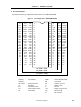
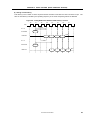
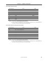
CHAPTER 1 PRODUCT OUTLINE
This chapter provides an outline of SDRAM products, taking the µPD45128163 128M SDRAM (512 K words × 16
bits × 4 banks) as examples. Unless otherwise specified, these models are treated as the representative products in
this User’s Manual.
14
User’s Manual E0123N50
CHAPTER 1 PRODUCT OUTLINE
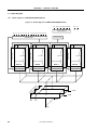
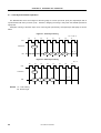
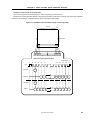
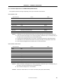
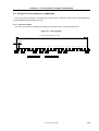
1.1 Pin Configuration
This section shows the pin configuration and pin names of the 64M/128M SDRAM.
Figure 1-1. Pin configuration of 64M/128M SDRAM
VCC
DQ0
VCCQ
DQ1
DQ2
VSSQ
DQ3
DQ4
VCCQ
DQ5
DQ6
VSSQ
DQ7
VCC
LDQM
/WE
/CAS
/RAS
/CS
A13
A12
A10
A0
A1
A2
A3
VCC
VCC
DQ0
VCCQ
NC
DQ1
VSSQ
NC
DQ2
VCCQ
NC
DQ3
VSSQ
NC
VCC
NC
/WE
/CAS
/RAS
/CS
A13
A12
A10
A0
A1
A2
A3
VCC
VCC
NC
VCCQ
NC
DQ0
VSSQ
NC
NC
VCCQ
NC
DQ1
VSSQ
NC
VCC
NC
/WE
/CAS
/RAS
/CS
A13
A12
A10
A0
A1
A2
A3
VCC
54
53
52
51
50
49
48
47
46
45
44
43
42
41
40
39
38
37
36
35
34
33
32
31
30
29
28
1
2
3
4
5
6
7
8
9
10
11
12
13
14
15
16
17
18
19
20
21
22
23
24
25
26
27
VSS
NC
VSSQ
NC
DQ3
VCCQ
NC
NC
VSSQ
NC
DQ2
VCCQ
NC
VSS
NC
DQM
CLK
CKE
NC
A11
A9
A8
A7
A6
A5
A4
VSS
VSS
DQ7
VSSQ
NC
DQ6
VCCQ
NC
DQ5
VSSQ
NC
DQ4
VCCQ
NC
VSS
NC
DQM
CLK
CKE
NC
A11
A9
A8
A7
A6
A5
A4
VSS
VSS
DQ15
VSSQ
DQ14
DQ13
VCCQ
DQ12
DQ11
VSSQ
DQ10
DQ9
VCCQ
DQ8
VSS
NC
UDQM
CLK
CKE
NC
A11
A9
A8
A7
A6
A5
A4
Vc
x4 (64M / 128M)
x8 (64M / 128M)
x16 (64M / 128M)
A0 - A13
: Address inputs
UDQM
: Upper DQ mask enable
A12 (BA1),
: Bank address
LDQM
: Lower DQ mask enable
CKE
: Clock enable
A13 (BA0)
DQ0 - DQ15
: Data inputs/outputs
CLK
: System clock input
/CS
: Chip select
VCC
: Supply voltage
/RAS
: Row address strobe
VSS
: Ground
/CAS
: Column address strobe
VCCQ
: Supply voltage for DQ
/WE
: Write enable
VSSQ
: Ground for DQ
NC
: No connection
User’s Manual E0123N50
15
CHAPTER 1 PRODUCT OUTLINE
1.2 Pin Functions
1.2.1 CLK input
An external clock is input to the CLK pin.
All input signals and data input/output signals are synchronized with the rising edge of CLK.
1.2.2 CKE input
CKE determines whether CLK is valid or not. If the CKE signal is high at the rising edge of a given CLK, the rising
edge of the next CLK is valid. Otherwise, the rising edge of the next CLK is invalid.
If the rising edge of CLK is invalid, the internal clock does not operate, and the product temporarily stops.
<Burst mode>
The internal burst clock temporarily stops if the CKE signal is made low in the burst mode.
<Self refresh mode>
Self refreshing is executed if the CKE signal is made low in the self refresh mode. In this mode, the CKE
signal must be kept low.
<Modes other than burst and self refresh modes>
In a mode other than the burst and self refresh modes, the power down mode is set if the CKE signal is made
low. In this mode, the CKE signal must be kept low.
1.2.3 /CS input
Low level: Starts a command input cycle.
High level: Command is ignored but the operation continues.
1.2.4 /RAS, /CAS, /WE input
/RAS, /CAS, and /WE have the same name as the signals of conventional DRAM but they differ in their function.
For details, refer to the list of commands.
1.2.5 VCC, VSS
Power supply pins. VCC and VSS are power supply pins for the internal circuit.
1.2.6 VCCQ, VSSQ
Power supply pins. VCCQ and VSSQ are power supply pins for the output buffer.
16
User’s Manual E0123N50
CHAPTER 1 PRODUCT OUTLINE
1.2.7 Address (A0 through Ax) input
<Row address>
Determined by A0 through Ax input when an active command is input.
<Column address>
Determined by A0 through Ax input when a read or write command is input.
<Bank address (BA)>
The bank to be selected differs depending on the input level of BA when a command is input.
<Precharge mode select address (AP)>
The function of this pin differs depending on the input level of AP when a precharge command is input or when
a read command (or write command) is input.
When precharge command is input
AP
Function
High level
Precharging all the banks is started (all bank precharge).
Low level
Precharging only the bank selected by a bank address is started.
When read/write command is input
AP
Function
High level
Precharge is automatically started after burst access (auto precharge).
Low level
Precharge command must be input to start precharge.
User’s Manual E0123N50
17
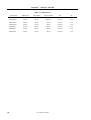
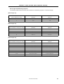
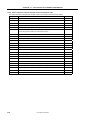
CHAPTER 1 PRODUCT OUTLINE
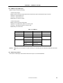
Table 1-1. Address Pins
Part Number
Address Pins
Row Address
Column Address
BA
AP
µPD45128441
A0-A13
A0-A11
A0-A9,A11
A12, A13
A10
µPD45128841
A0-A13
A0-A11
A0-A9
A12, A13
A10
µPD45128163
A0-A13
A0-A11
A0-A8
A12, A13
A10
µPD4564441
A0-A13
A0-A11
A0-A9
A12, A13
A10
µPD4564841
A0-A13
A0-A11
A0-A8
A12, A13
A10
µPD4564163
A0-A13
A0-A11
A0-A7
A12, A13
A10
SDRAM
18
User’s Manual E0123N50
CHAPTER 1 PRODUCT OUTLINE
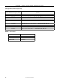
1.2.8 DQM0 through DQM3 input
DQM is used to control the I/O buffer.
<Read mode (output)>
DQM is used to control the output buffer and is the same as the conventional /OE pin in function.
High level: Output buffer is off.
Low level : Output buffer is on.
DQM latency for read is 2 clocks.
<Write mode (input)>
DQM is used to control the word mask.
High level: Input data is not written to a memory cell.
Low level : Input data is written to a memory cell.
DQM latency for write is zero.
Table 1-2. DQM Pin
Bit Organization
Control Pin
Part Number
×4 bits
DQM
DQ0-DQ3
µPD45128441
×8 bits
DQM
DQ0-DQ7
µPD45128841
×16 bits
LDQM
DQ0-DQ7
µPD45128163
UDQM
DQ8-DQ15
DQM0
DQ0-DQ7
DQM1
DQ8-DQ15
DQM2
DQ16-DQ25
DQM3
DQ26-DQ31
×32 bits
Remark
Pin Name
µPD4564323
DQM latency is the number of clocks necessary for controlling the I/O buffer after DQM has been made
high.
1.2.9 DQ0 through DQx I/O
The function of the DQ pin is the same as that of the I/O pin of conventional DRAM.
User’s Manual E0123N50
19
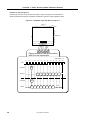
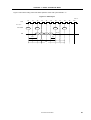
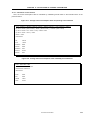
CHAPTER 1 PRODUCT OUTLINE
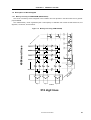
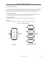
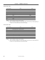
1.3 Block Diagram
1.3.1 Block diagram of 128M SDRAM (µPD45128163)
Figure 1-2. Block diagram of 128M SDRAM (µPD45128163)
CLK CKE /CS /RAS /CAS /WE
Vss Vcc
Timing Generator
A6 A7 A8 A9 A10 A11 A12 A13
Address Buffer
Refresh Counter
4 K Rows
512 columns
Row Decoder
512 columns
Row Decoder
Row Decoder
512 columns
4 K Rows
Memory Cell Array
Memory Cell Array
Bank A
4 K Rows
Memory Cell Array
Bank B
512 columns
Row Decoder
A0 A1 A2 A3 A4 A5
4 K Rows
Memory Cell Array
Bank C
Bank D
Sense Amp.
Sense Amp.
Sense Amp.
Column Decoder
Column Decoder
Column Decoder
do
m
I/O
Bu
ffe
r
Sense Amp.
Column Decoder
R
an
UDQM
LDQM
DQ15
VCCQ
VSSQ
DQ0
20
User’s Manual E0123N50
CHAPTER 1 PRODUCT OUTLINE
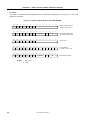
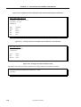
1.4 Description of Block Diagram
1.4.1 Memory cell array of 128M SDRAM (µPD45128163)
The circuit of a memory cell is configured of one transistor and one capacitor in the same manner as a generalpurpose DRAM.
The µPD45128163 (×16-bit organization) has a total capacity of 128M bits and consists of 4096 word lines, 512
digit lines, 16 I/O lines, and four banks.
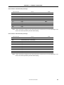
Word 1
Word 2
Word 3
Word 4
16
Word 4096
I/O
4096 word lines
Figure 1-3. Memory Cell Array (128M SDRAM)
Digit 1
Digit 2
Digit 512
512 digit lines
User’s Manual E0123N50
21
CHAPTER 1 PRODUCT OUTLINE
1.4.2 Address (Row, Column) decoders
These products employ an address multiplex method. To decode a certain address, a bank select signal and a
row address are loaded at the same time as an active command, and the corresponding word line is selected. Next,
a bank select signal and a column address are loaded at the same time as a read command or write command, the
corresponding digit line is selected, and an address is decoded.
1.4.3 I/O buffer
Buffer for data input/output.
1.4.4 Refresh counter
This counter automatically counts row addresses in the memory.
22
User’s Manual E0123N50
CHAPTER 2 FEATURES OF PRODUCTS
Elpida memory’s SDRAM can access successive data at high speeds in synchronization with a system clock of
133 MHz at a voltage of as low as 3.3 V.
This chapter explains the following basic features of the SDRAM.
(1) Clock synchronization operation
(2) Control by command
(3) Plural bank configuration
(4) Burst transfer
(5) Comparison with general-purpose DRAM
User’s Manual E0123N50
23
CHAPTER 2 FEATURES OF PRODUCTS
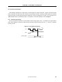
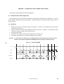
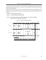
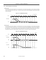
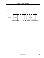
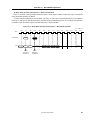
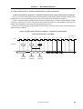
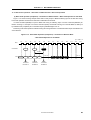
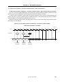
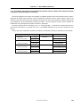
2.1 Clock Synchronization Operation
The SDRAM latch each control signal at the rising edge of a basic input clock (CLK) and input/output data in
synchronization with the input clock (CLK). Therefore, designing the timing is easy when the SDRAM operates at
high speed.
Examples of timing of the basic input clock, control signals (commands), and input/output data (DQ) are shown
below.
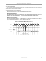
Figure 2-1. Read Cycle Timing
CL = 2, BL = 4
T0
T1
T2
T3
T4
T5
T6
T7
CLK
Command
READ
Hi - Z
Q0
DQ
Q1
Q2
Q3
Figure 2-2. Write Cycle Timing
BL = 4
T0
T1
T2
T3
T4
T5
T6
CLK
Command
WRIT
Hi - Z
DQ
Remark
D0
D1
D2
D3
CL: /CAS Latency
BL: Burst Length
24
User’s Manual E0123N50
T7
CHAPTER 2 FEATURES OF PRODUCTS
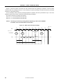
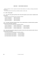
2.2 Control by Command
With SDRAM, combinations of logic levels of control signals are called commands. Typical commands include
active command, read command, write command, and precharge command. Although control signals are combined
at logic level when controlling general-purpose DRAM, the concept of commands is not used. The commands of the
128M SDRAM is listed on the following page. For examples of command operations, refer to Chapter 7.
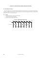
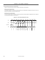
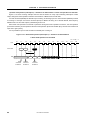
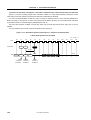
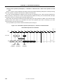
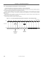
2.2.1 Command input timing
All the commands are latched in synchronization with the rising edge of CLK. To activate CLK, signal CKE is
used. When inputting a command, a high level must be input to CKE at the timing of CLK “n – 1” where “n” indicates
the rising of CLK.
Figure 2-3. Command Input Timing
n–1
n
n+1
CLK
CKE
Control signals
H
Command
User’s Manual E0123N50
25
CHAPTER 2 FEATURES OF PRODUCTS
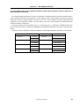
2.2.2 SDRAM command list
The commands of the 128M SDRAM are listed below.
Table 2-1. 128M SDRAM (×
×4/×
×8/×
×16-bit organization) Command List
No
Command
CKE
Symbol
n–1
/CS
/RAS
/CAS
/WE
Address
DQM
n
BA0,
A10
BA1
A9-A0
A11
1
Mode register set
MRS
H
×
L
L
L
L
×
L
L
V
2
CBR (auto) refresh
REF
H
H
L
L
L
H
×
×
×
×
3
Self refresh start
SELF
H
L
L
L
L
H
×
×
×
×
4
Self refresh exit
–
L
H
L
H
H
H
×
×
×
×
H
×
×
×
×
×
×
×
5
Precharge select bank
PRE
H
×
L
L
H
L
×
V
L
×
6
Precharge all banks
PALL
H
×
L
L
H
L
×
×
H
×
7
Bank active
ACT
H
×
L
L
H
H
×
V
V
V
8
Write
WRIT
H
×
L
H
L
L
×
V
L
V
9
Write (with auto precharge)
WRITA
H
×
L
H
L
L
×
V
H
V
READ
H
×
L
H
L
H
×
V
L
V
READA
H
×
L
H
L
H
×
V
H
V
12 Burst stop
BST
H
×
L
H
H
L
×
×
×
×
13 No operation
NOP
H
×
L
H
H
H
×
×
×
×
14 Device deselect
DESL
H
×
H
×
×
×
×
×
×
×
15 Data input/output enable
-
H
×
×
×
×
×
L
×
×
×
16 Data mask
-
H
×
×
×
×
×
H
×
×
×
10 Read
11 Read (with auto precharge)
Remark
26
H: High level, L: Low level, ×: High or low level (Don’t care), V: Valid data
User’s Manual E0123N50
CHAPTER 2 FEATURES OF PRODUCTS
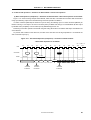
2.3 Plural Bank Configuration
The SDRAM divide the internal circuits of the chip (address decoder, memory cell arrays, and sense amplifier)
into plural banks. Each bank can be controlled independently. With this configuration and by making the best use of
the interleave operation of each bank, another bank can be accessed even while one bank is precharged.
2.3.1 Four-bank configuration
A four-bank model has four banks: A, B, C, and D. These banks are selected by a bank address (BA0 or BA1).
The four-bank model is outlined below through comparison with general-purpose DRAM.
General-purpose DRAM
To use four banks, four devices are necessary. These banks are selected by the /RAS signal.
SDRAM
Because four banks are provided to a device, four banks can be configured with one device.
Figure 2-4. Four-Bank Configuration
/RAS1
BANK A
/RAS2
BANK B
BANK A
BANK B
BA0
BA1
Data In
Data Out
Data In
Data Out
BANK C
/RAS3
BANK C
/RAS4
BANK D
BANK D
SDRAM
General-purpose DRAM
User’s Manual E0123N50
27
CHAPTER 2 FEATURES OF PRODUCTS
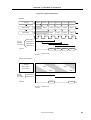
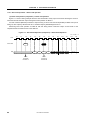
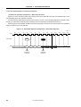
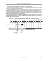
2.4 Burst Transfer
Because the SDRAM internally perform pipeline processing, they can successively input/output a fixed number of
memory data in synchronization with an external clock.
Pipeline processing divides the operations, including column address input and data input/output, into several
blocks and executes these blocks in parallel, in order to enhance the data transfer capability.
Figure 2-6 illustrates the concept of three-stage pipeline architecture, comparing it with that of the generalpurpose DRAM.
(1) General-purpose DRAM
The next operation cannot be started until a series of operations, from address input to data output, has been
completed.
(2) SDRAM
A column operation is divided into three operation blocks. When one operation block has been completed, the
operation can proceed to the next operation block. When a column address is input, the internal column
address counter automatically increments the internal column address in synchronization with the clock. The
number by which the column address is to be incremented is determined by the burst length. This internal
structure enables reading or writing of data of successive addresses.
(3) Comparison between general-purpose DRAM and SDRAM
The time for the first data to be output is the same for general-purpose DRAM and SDRAM.
When plural data are successively input/output, however, the SDRAM that perform parallel processing as
described in (2) can transfer data at high speeds.
28
User’s Manual E0123N50
CHAPTER 2 FEATURES OF PRODUCTS
Figure 2-5. Pipeline Architecture
SDRAM
Y - Decoder
Address 1 Address 2
Data amplifer
Address 3 Address 4
Data 1
Output buffer
T1
T2
Address 5 Address 6
Data 2
Data 3
Data 4
Data 5
Data 1
Data 2
Data 3
Data 4
T3
T4
T5
T6
Data1
Data2
Data3
Data4
Output data 1
Time for
each data
to be output
Output data 2
Output data 3
Output data 4
Data out
Unused portion
General-purpose DRAM
Address 1
Address 2
Y - Decoder
Data amplifer
Data 1
Data 2
Output buffer
Time for
each data
to be output
Data 1
Data 2
Data1
Data2
Output data 1
Output data 2
Data out
Unused portion
User’s Manual E0123N50
29
CHAPTER 2 FEATURES OF PRODUCTS
2.5 Comparison with General-Purpose DRAM
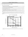
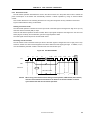
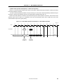
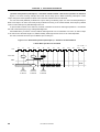
2.5.1 Increasing speed of DRAM
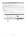
The figure below compares the access times of the SDRAM and an EDO DRAM.
Although there is not much difference in /RAS access time (random access time), the burst cycle time of SDRAM
is much shorter than the burst cycle time of EDO DRAM.
There is not much difference in the /RAS access time between SDRAM and EDO DRAM because their internal
basic configurations are almost the same.
However, SDRAM can shorten the burst cycle time, as compared with general-purpose DRAM, by employing
techniques different from those of general-purpose DRAM, such as pipelining.
Generally, EDO DRAM is synchronized with a 66-MHz (15-ns) clock. In contrast, SDRAM is planned to be
synchronized with a 133-MHz (7.5-ns) clock. Synchronization with a clock of more than 200 MHz is also under
study.
As the frequency of the clock system increases in the future, it is expected that the performance of systems can
be improved by employing SDRAM instead of EDO DRAM when a system with a memory clock of 75 MHz or more is
designed.
Figure 2-6. Increasing Speed of DRAM
35
General-purpose DRAM
(EDO DRAM, etc.)
Burst cycle time (ns)
30
25
20
15
10
Synchronous DRAM
5
80
70
60
50
40
30
/RAS access time (ns)
Remark
30
The burst cycle time indicates the /CAS cycle time of DRAM and the clock cycle time of SDRAM.
User’s Manual E0123N50
CHAPTER 2 FEATURES OF PRODUCTS
2.5.2 Basic control method and access time
The actual control method is explained, taking the read cycle as an example.
(1) Basic control method
Figure 2-7. Read Cycle of SDRAM and General-Purpose DRAM
SDRAM
T0
T1
T2
T3
T4
T5
T6
T7
T8
T9
T10
CLK
tRAS
Command
ACT
READ
Address
Row
Col.
tRCD
PRE
ACT
Row
/CAS latency=2
Data out
Hi - Z
Dout
General-purpose DRAM
tRAS
/RAS
/CAS
/WE
High level
tRCD
/CAS access time
Hi - Z
Data out
Dout
<1>
<2>
<3>
Caution General-purpose DRAM is asynchronous.
User’s Manual E0123N50
31
CHAPTER 2 FEATURES OF PRODUCTS
Timing <1>
SDRAM: Input of active command (ACT)
General-purpose DRAM: Status in which the /RAS signal goes low when the /CAS signal is high
Timing <2>
SDRAM: Input of read command (READ)
General-purpose DRAM: Status in which the /CAS signal goes low when the /RAS signal is low and when the
/WE signal is high
SDRAM: /CAS latency
(Number of clocks since a column address signal has been latched until the valid data is output)
General-purpose DRAM: /CAS access time
SDRAM: Input of burst length (number of words of data successively output)
General-purpose DRAM: Number of page mode cycles
Timing <3>
SDRAM: Input of precharge command (PRE)
General-purpose DRAM: Status in which the /RAS and /CAS signals go high
32
User’s Manual E0123N50
CHAPTER 2 FEATURES OF PRODUCTS
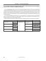
(2) Access time
The following figure indicates the bust read cycle where burst length = 4. The access time of this SDRAM is
compared with the access time of an EDO DRAM with a /RAS access time of 60 ns, assuming that the clock rate
of the SDRAM is 66 MHz.
Figure 2-8. Burst Read Cycle
SDRAM
T0
T1
T2
T3
T4
T5
T6
T7
T8
Dout
Dout
Dout
T9
T10
CLK
15 ns
Command
ACT
READ
Address
Row
Col.
Hi - Z
Data out
Dout
60 ns
General-purpose DRAM
/RAS
/CAS
25 ns
/WE
High level
Data out
Dout
60 ns
Dout
Dout
Dout
Table 2-2. Comparison of Access Time of SDRAM and EDO DRAM
Access Time
SDRAM
EDO DRAM
Comparison
First access time
60 ns
60 ns
Same
Second access time
75 ns
85 ns
SDRAM is shorter by 10 ns.
Third access time
90 ns
110 ns
SDRAM is shorter by 20 ns.
Fourth access time
105 ns
135 ns
SDRAM is shorter by 30 ns.
The first access times of SDRAM and EDO DRAM are the same. As the burst length increases, however, the
transfer speed of SDRAM goes up.
User’s Manual E0123N50
33
CHAPTER 2 FEATURES OF PRODUCTS
The following table compares the access times of various SDRAMs and EDO DRAMs.
Table 2-3. Access Times of SDRAMs and EDO DRAMs
Grade
SDRAM
EDO DRAM
First Access
Second Access
Third Access
Fourth Access
133 MHz (7.5 ns)
45 ns
52.5 ns
59 ns
66.5 ns
125 MHz (8 ns)
40 ns
48 ns
56 ns
64 ns
100 MHz (10 ns)
50 ns
60 ns
70 ns
80 ns
66 MHz (15 ns)
60 ns
75 ns
90 ns
105 ns
−60
60 ns
85 ns
110 ns
135 ns
−50
50 ns
70 ns
90 ns
110 ns
The first access times of SDRAM: 100 MHz (10 ns) and EDO DRAM: −50 are the same.
However, the
difference between SDRAM and EDO DRAM is evident at the fourth access. Although the above table shows
data of up to burst length = 4, SDRAM is superior to EDO DRAM in data transfer capability as the burst length
increases.
34
User’s Manual E0123N50
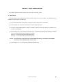
CHAPTER 3 OPERATION AFTER POWER APPLICATION
This chapter explains initialization after power application.
3.1 Initialization after Power Application
The logical status of the internal circuit of SDRAM is undefined immediately after power application. To ensure
correct operation, SDRAM must always be initialized. Unless initialization is correctly executed, the device may not
operate correctly.
3.2 Initializing
1.
Supply power and clock. At this time, make sure that CKE = H, DQM = H, and maintain the other input pins
in the NOP or DESL status.
2.
After the power and clock have been stabilized, make sure that CKE = H, DQM = H, and maintain the other
input pins in the NOP or DESL status for at least 200 µs.
3.
Precharge all the banks.
4.
Execute the auto refresh command at least eight times as a dummy cycle.
5.
Execute the mode register set command to initialize the mode register.
Cautions
To ensure that the output goes into a high-impedance state after the pause period of at least
200 µs in step 2 above, keep CKE and DQM high until the precharge command is input.
Figure 3-1. Initializing SDRAM
VCC
VCC(MIN.)
CLK
CKE
H
tRP
tRC
t RC
t RSC
Pause period of at least 200 µs
Command
DQM
PALL
REF
REF
MRS
CMD
H
User’s Manual E0123N50
35
CHAPTER 4 BASIC SETTING (MODE REGISTER SETTING)
4.1 Mode Register Setting
The mode register sets the operation modes of SDRAM, such as the latency mode, wrap type, and burst length.
At this time, addresses A0 through Ax are used as input data. Once the mode register has been set, it holds the set
data until it is reset or the power is turned off.
4.1.1 Setting
1
Execute the precharge command to all the banks.
→ Set all the banks in the idle status.
2.
Execute the mode register set command.
Figure 4-1. Mode Register Setting Cycle
T0
T1
T2
T3
T4
T5
T6
CLK
Command
PALL
MRS
tRP
36
User’s Manual E0123N50
ACT
t RSC
T7
CHAPTER 4 BASIC SETTING (MODE REGISTER SETTING)
4.1.2 Set parameters
The mode register has the following four functions:
(1) A0 through A2 : Sets a burst length.
(2) A3
: Sets a wrap type.
(3) A4 through A6 : Sets a /CAS latency.
(4) A7 through Ax : Option
(1) Setting of burst length
The burst length is the number of data that can be successively input or output. The burst length may be 1, 2, 4,
8, or full page.
User’s Manual E0123N50
37
CHAPTER 4 BASIC SETTING (MODE REGISTER SETTING)
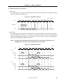
Example 1) Burst length of 8
Data of eight columns can be successively input or output by inputting a command once.
When the read burst has been completed, the data bus goes into a high-impedance state.
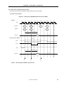
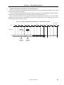
Figure 4-2. Read/Write Cycle with Burst Length of 8
512 Col.
511
4095
0
4096 Row
0
0
1
2
3
4
5
6
7
Eight successive data synchronized
with CLK are input/output.
/CAS latency = 2
T-1
T0
T1
T2
T3
T4
T5
T6
T7
T8
T9
T10
T11
CLK
Command
READ
Data Out
38
Command
WRIT
Data In
0
1
0
1
2
3
4
5
2
3
4
5
6
7
User’s Manual E0123N50
6
7
Hi-Z
Hi-Z
CHAPTER 4 BASIC SETTING (MODE REGISTER SETTING)
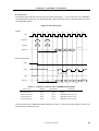
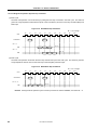
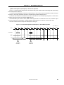
Example 2) Burst length of full page (512)
Data of a full page are successively input or output by inputting a command once.
Because the input/output data perform a wrap-around operation at this time, the burst stop command, read/write
command, and precharge command must be used to stop input/output of data.
Figure 4-3. Read/Write Cycle with Burst Length of Full Page (256)
512 Col.
0
511
4095
4096 Row
0
0
1
2
3
508 509 510 511
256 successive data synchronized
with CLK are input/output.
/CAS latency = 2
T-1
T0
T1
T2
T3
T4
T511 T512
T513 T514
T515
CLK
Command
READ
Data Out
Command
WRIT
Data In
0
1
0
1
508 509 510 511
0
2
3
510 511
2
User’s Manual E0123N50
0
1
39
CHAPTER 4 BASIC SETTING (MODE REGISTER SETTING)
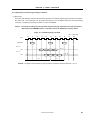
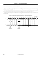
(2) Setting of wrap type
The wrap type specifies the sequence in which the address of burst data is incremented. SDRAM supports the
sequential type and interleave type. When A3 = 0, the sequential type is selected; when A3 = 1, the interleave
type is selected. Which type is to be selected is determined by the type of CPU used in each system.
Figure 4-4. Wrap Type
Interleave
Sequential
Start address
A
Carry
Start address
A
A+B
Addr
Binary counter
40
B
A + B Sequential
address
Binary counter
User’s Manual E0123N50
B
Interleave
address
CHAPTER 4 BASIC SETTING (MODE REGISTER SETTING)
Burst length and addressing sequence
The following tables indicate the start column address and addressing sequence of each burst length.
[Burst length = 2]
Start Address
(column address A0, binary)
Sequential Addressing Sequence
(decimal)
Interleave Addressing Sequence
(decimal)
0
0, 1
0, 1
1
1, 0
1, 0
Start Address
(column address A1 through A0, binary)
Sequential Addressing Sequence
(decimal)
Interleave Addressing Sequence
(decimal)
00
0, 1, 2, 3
0, 1, 2, 3
01
1, 2, 3, 0
1, 0, 3, 2
10
2, 3, 0, 1
2, 3, 0, 1
11
3, 0, 1, 2
3, 2, 1, 0
Start Address
(column address A2 through A0, binary)
Sequential Addressing Sequence
(decimal)
Interleave Addressing Sequence
(decimal)
000
0, 1, 2, 3, 4, 5, 6, 7
0, 1, 2, 3, 4, 5, 6, 7
001
1, 2, 3, 4, 5, 6, 7, 0
1, 0, 3, 2, 5, 4, 7, 6
010
2, 3, 4, 5, 6, 7, 0, 1
2, 3, 0, 1, 6, 7, 4, 5
011
3, 4, 5, 6, 7, 0, 1, 2
3, 2, 1, 0, 7, 6, 5, 4
100
4, 5, 6, 7, 0, 1, 2, 3
4, 5, 6, 7, 0, 1, 2, 3
101
5, 6, 7, 0, 1, 2, 3, 4
5, 4, 7, 6, 1, 0, 3, 2
110
6, 7, 0, 1, 2, 3, 4, 5
6, 7, 4, 5, 2, 3, 0, 1
111
7, 0, 1, 2, 3, 4, 5, 6
7, 6, 5, 4, 3, 2, 1, 0
[Burst length = 4]
[Burst length = 8]
User’s Manual E0123N50
41
CHAPTER 4 BASIC SETTING (MODE REGISTER SETTING)
[Full-page burst (column length: 512)]
Start Address
(column address A7 through A0, binary)
000000000
0, 1, 2, 3, 4, 5, 6, 7, 8, 9, 10, ……. 506, 507, 508, 509, 510, 511
000000001
1, 2, 3, 4, 5, 6, 7, 8, 9, 10, ……. 506, 507, 508, 509, 510, 511, 0
000000010
2, 3, 4, 5, 6, 7, 8, 9, 10, ……. 506, 507, 508, 509, 510, 511, 0, 1
000000011
3, 4, 5, 6, 7, 8, 9, 10, ……. 506, 507, 508, 509, 510, 511, 0, 1, 2
:
:
Remark
:
:
111111100
508, 509, 510, 511, 0, 1, 2, 3, 4, 5, 6, ……. 502, 503, 504, 505, 506, 507
111111101
509, 510, 511, 0, 1, 2, 3, 4, 5, 6, 7, ……. 503, 504, 505, 506, 507, 508
111111110
510, 511, 0, 1, 2, 3, 4, 5, 6, 7, 8, ……. 504, 505, 506, 507, 508, 509
111111111
511, 0, 1, 2, 3, 4, 5, 6, 7, 8, 9, ……. 505, 506, 507, 508, 509, 510
Column length
Part Number
42
Sequential Addressing Sequence
(decimal)
Full Column Length
µPD45128441
2,048 columns
µPD45128841
1,024 columns
µPD45128163
512 columns
User’s Manual E0123N50
CHAPTER 4 BASIC SETTING (MODE REGISTER SETTING)
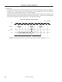
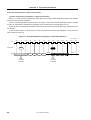
(3) Setting of /CAS latency
/CAS latency is the number of clocks required until the first data is read after the read command is input. The
value of /CAS latency is limited by the operating frequency of the clock and speed grade of the SDRAM.
Figure 4-5. Timing Differences between /CAS Latency = 2 and 3
T0
T1
T2
T3
T4
T5
T6
T7
CLK
2 clocks
CL = 2
Command
Read
Hi-Z
0
Data Out
Data Out
2
3
0
1
2
3 clocks
CL = 3
Command
1
Read
Hi-Z
User’s Manual E0123N50
3
43
CHAPTER 4 BASIC SETTING (MODE REGISTER SETTING)
(4) Option
The mode is changed as follows depending on the information on addresses A7 through A13 of the mode
register set command.
Figure 4-6. Options in Mode Register (with 128M SDRAM)
13
12
11
10
9
8
7
0
0
0
0
0
0
1
13
12
11
10
9
8
7
x
x
x
x
1
0
0
13
12
11
10
9
8
7
1
0
6
5
4
3
1
0
JEDEC standard test set
(refresh counter test)
6
5
4
LTMODE
6
5
3
2
WT
4
3
1
0
Burst read & single write
(for write through cache)
BL
2
1
0
Use in future
13
12
11
10
9
8
7
6
5
4
3
2
1
0
x
x
x
x
x
1
1
V
V
V
V
V
V
V
13
12
11
10
9
8
7
6
5
4
3
2
1
0
0
0
0
0
0
0
0
Remark
LTMODE
WT
×: Don’t care
V: Valid
44
2
User’s Manual E0123N50
BL
Vendor-specific
(V: Valid, ×: Don’t care)
Mode register setting
CHAPTER 4 BASIC SETTING (MODE REGISTER SETTING)
4.1.3 Setting of burst length, wrap type, and /CAS latency
To set the burst length, wrap type, and /CAS latency, set the option of mode register setting (A7 through A13:
0000000) by using the mode register set command.
Although the burst length, wrap type, and /CAS latency can also be set by means of burst read and single write
(A7, A8, A9: 001), the burst length of the write cycle is set to 1 in this case.
Figure 4-7. Field of Mode Register (with 128M SDRAM)
13
12
11
10
9
8
7
x
x
x
x
1
0
0
13
12
11
10
9
8
7
0
0
0
0
0
0
0
6
5
4
LTMODE
6
5
3
2
1
WT
4
LTMODE
3
0
Burst read & single write
(for write through cache)
BL
2
1
WT
0
Mode register setting
BL
Burst length
A2
A1
A0
WT = 0
WT = 1
0
0
0
1
1
0
0
1
2
2
0
1
0
4
4
0
1
1
8
8
1
0
0
R (reserved)
R (reserved)
1
0
1
R (reserved)
R (reserved)
1
1
0
R (reserved)
R (reserved)
1
1
1
Full page
R (reserved)
Wrap type
A3
Wrap type (WT)
0
Sequential
1
Interleave
/CAS latency
A6
A5
A4
/CAS latency
0
0
0
R (reserved)
0
0
1
R (reserved)
0
1
0
2
0
1
1
3
1
0
0
R (reserved)
1
0
1
R (reserved)
1
1
0
R (reserved)
1
1
1
R (reserved)
User’s Manual E0123N50
45
CHAPTER 5 STATUS TRANSITIONS
This chapter explains the status transitions of SDRAM.
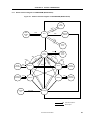
5.1 Status Transition Diagram
Figure 5-1 shows the status transition diagram of SDRAM. The circles in the figure indicate the device status,
and the status is changed in the direction indicated by the arrow.
46
User’s Manual E0123N50
CHAPTER 5 STATUS TRANSITIONS
5.1.1 Status transition diagram of 128M SDRAM (µPD45128163)
Figure 5-1. Status Transition Diagram of 128M SDRAM (µPD45128163)
Self
Refresh
LF
SE
t
LF
exi
SE
MRS
Mode
Register
Set
REF
IDLE
CBR (Auto)
Refresh
CK
E
ACT
CK
E
Power
Down
CKE
ROW
ACTIVE
BS
T
ite
wit
pre h
ch
arg
Wr
CKE
Read
ad
WRITE
CKE
CKE
WRITEA
CKE
Precharge
PR
E(
Pre
cha
rge
ter
min
atio
n)
Write
CKE
POWER
ON
Read
READ
n)
atio
min
ter
rge
cha
Pre
E(
PR
WRITEA
SUSPEND
Au
WRITE
SUSPEND
to
W
T
Re
h
wit e
ad
rg
Re cha
pre
to
PRE
Write
Au
e
rit
e
BS
Active
Power
Down
CKE
CKE
CKE
READA
CKE
READ
SUSPEND
READA
SUSPEND
Precharge
Automatic sequence
Manual input
User’s Manual E0123N50
47
CHAPTER 5 STATUS TRANSITIONS
5.2 Status Description
This section explains the statuses of SDRAM.
5.2.1 Idle
The idle status is the status from which all operations are started. Commands such as the active command,
register set command, and refresh command must be input when the device (the bank to be selected) is in the idle
status.
5.2.2 Row active
In the row active status, a row address is selected and an operation request (read command or write command) is
not made. To change the status from idle to row active, input an active command to the selected row address.
5.2.3 Precharge
In the precharge status, the operation to the current row address ends and an operation to another row address is
started. When the precharge command is input, the device automatically returns to the idle status.
5.2.4 Read and write
In the read or write status, the read or write operation is executed. To change the status from row active to this
status, input the read or write command to the selected column address. When the read or write operation is
completed, the device automatically returns to the row active status.
5.2.5 Read and write with auto precharge
When the read or write command with auto precharge is input, the device automatically starts precharging and
returns to the idle status after the read or write operation is completed.
48
User’s Manual E0123N50
CHAPTER 5 STATUS TRANSITIONS
5.2.6 Suspend
If the CKE pin goes low during read operation or write operation (including read and write with auto precharge),
the operation is temporarily stopped.
5.2.7 Mode register setting
The mode register can be set when all banks of the device are in the idle status. When data has been written to
the mode register, the device automatically returns to the idle status.
5.2.8 CBR (auto) refresh
The CBR refresh command can be executed when all banks of the device are in the idle status. When the CBR
refresh command is input, a certain row address of all banks is selected, and refreshing is executed. When CBR
refreshing is completed, the device automatically returns to the idle status.
5.2.9 Self refresh
The self refresh command can be executed when all banks of the device are in the idle status, like the CBR
refresh command. In the self refresh status, the device automatically performs refreshing. During this time, it is not
necessary to execute the refresh command from an external source. When the device exits from the self refresh
status, it automatically returns to the idle status.
5.2.10 Power down
If CKE is made low in the idle status or row active status, the power down mode is set. In this mode, all input
buffers except CLK and CKE are off, and the power consumption of the device is lowered. To return to the original
status (idle or active), make CKE high.
User’s Manual E0123N50
49
CHAPTER 6 COMMAND OPERATIONS
This chapter explains the points to be noted in executing commands.
For command lists, refer to 2.2.2 SDRAM command list, 5.1.1 Status transition diagram of 128M SDRAM.
6.1 Command Execution Condition
The status in which each command can be executed is shown below.
Table 6-1. Command Executable Condition
Command
Symbol
Command Executable (Input) Condition
Mode register set
MRS
All banks are in idle status.
CBR (auto) refresh
REF
All banks are in idle status.
Self refresh
SELF
All banks are in idle status.
Precharge select bank
PRE
tRAS after active command input (selected bank)
Precharge all banks
PALL
tRAS after active command input (all banks)
Bank active
ACT
Selected bank is in idle status.
Write
WRIT
tRCD after active command input (selected bank)
Write with auto precharge
WRITA
tRCD after active command input (selected bank)
Read
READ
tRCD after active command input (selected bank)
Read with auto precharge
READA
tRCD after active command input (selected bank)
Burst stop
BST
During read or write operation
No operation
NOP
All status
Device deselect
DESL
All status
50
User’s Manual E0123N50
Remark
CHAPTER 6 COMMAND OPERATIONS
6.2 Command Operations of 128M SDRAM (µPD45128163)
The operation status that changes depending on the input command is shown below.
Current status: Idle
Input Command
Action
Notes
DESL
NOP or power down
Note 1
NOP
NOP or power down
Note 1
BST
NOP or power down
Note 1
READ/READA
Illegal
Note 2
WRIT/WRITA
Illegal
Note 2
ACT
Row activating
PRE/PALL
NOP
Note 3
REF/SELF
CBR (auto) refresh/self refresh
Note 4
MRS
Mode register set
Note 5
Notes 1. If all banks are in the idle status and CKE is inactive (low level), the power down mode is set.
2. These commands are illegal for the same bank (these commands may be valid depending on
the status of the bank specified by the bank address (BA)).
3. Precharging is enabled depending on the status of the bank specified by the bank address (BA).
4. If all banks are in the idle status and CKE is inactive (low level), the self refresh mode is set.
5. This command is illegal if there is a bank that is not in the idle status.
Current status: Row active
Input Command
Action
Notes
DESL
NOP
NOP
NOP
BST
NOP
READ/READA
Begin read: Determine AP
WRIT/WRITA
Begin write: Determine AP
ACT
Illegal
Note 1
PRE/PALL
Precharge
Note 2
REF/SELF
Illegal
MRS
Illegal
Notes 1. These commands are illegal for the same bank (these commands may be valid depending on
the status of the bank specified by the bank address (BA)).
2. This command is illegal if tRAS is not satisfied.
Remark
Row active: Status after tRCD from active command (ACT) input (selected bank)
User’s Manual E0123N50
51
CHAPTER 6 COMMAND OPERATIONS
Current status: Read
Input Command
Action
Notes
DESL
Continue burst to end → Row active
NOP
Continue burst to end → Row active
BST
Burst stops → Row active
READ/READA
Burst stops → Start read: Determine AP
Note 1
WRIT/WRITA
Burst stops → Start write: Determine AP
Note 1
ACT
Illegal
Note 2
PRE/PALL
Burst stops → precharging
REF/SELF
Illegal
MRS
Illegal
Notes 1. The burst interrupt condition must be satisfied.
2. These commands are illegal for the same bank (these commands may be valid depending on
the status of the bank specified by the bank address (BA)).
Current status: Write
Input Command
Action
Notes
DESL
Continue burst to end → Write recovering
NOP
Continue burst to end → Write recovering
BST
Burst stops → Row active
READ/READA
Burst stops → Start read: Determine AP
Note 1
WRIT/WRITA
Burst stops → Start write: Determine AP
Note 1
ACT
Illegal
Note 2
PRE/PALL
Burst stops → precharging
Note 1
REF/SELF
Illegal
MRS
Illegal
Notes 1. The burst interrupt condition must be satisfied.
2. These commands are illegal for the same bank (these commands may be valid depending on
the status of the bank specified by the bank address (BA)).
52
User’s Manual E0123N50
CHAPTER 6 COMMAND OPERATIONS
Current status: Read with auto precharge
Input Command
Action
Notes
DESL
Continue burst to end → Precharging
NOP
Continue burst to end → Precharging
BST
Illegal
READ/READA
Illegal
Note
WRIT/WRITA
Illegal
Note
ACT
Illegal
Note
PRE/PALL
Illegal
Note
REF/SELF
Illegal
MRS
Illegal
Note These commands are illegal for the same bank (these commands may be valid depending on the
status of the bank specified by the bank address (BA)).
Current status: Write with auto precharge
Input Command
Action
Notes
DESL
Continue burst to end → Precharging
NOP
Continue burst to end → Precharging
BST
Illegal
READ/READA
Illegal
Note
WRIT/WRITA
Illegal
Note
ACT
Illegal
Note
PRE/PALL
Illegal
Note
REF/SELF
Illegal
MRS
Illegal
Note These commands are illegal for the same bank (these commands may be valid depending on the
status of the bank specified by the bank address (BA)).
User’s Manual E0123N50
53
CHAPTER 6 COMMAND OPERATIONS
Current status: Precharging
Input Command
Action
Notes
DESL
NOP → Enter idle after tRP
NOP
NOP → Enter idle after tRP
BST
Illegal
READ/READA
Illegal
Note 1
WRIT/WRITA
Illegal
Note 1
ACT
Illegal
Note 1
PRE/PALL
NOP → Enter idle after tRP
Note 2
REF/SELF
Illegal
MRS
Illegal
Notes 1. These commands are illegal for the same bank (these commands may be valid depending on
the status of the bank specified by the bank address (BA)).
2. Precharging is enabled depending on the status of the bank specified by the bank address
(BA).
Current status: Row activating
Input Command
Action
Notes
DESL
NOP → Enter bank active after tRCD
NOP
NOP → Enter bank active after tRCD
BST
Illegal
READ/READA
Illegal
Note 1
WRIT/WRITA
Illegal
Note 1
ACT
Illegal
Notes 1, 2
PRE/PALL
Illegal
Note 1
REF/SELF
Illegal
MRS
Illegal
Notes 1. These commands are illegal for the same bank (these commands may be valid depending on
the status of the bank specified by the bank address (BA)).
2. This command is illegal if tRRD is not satisfied.
Remark
54
Row activating: Status of less than tRCD from active command (ACT) input (selected bank)
User’s Manual E0123N50
CHAPTER 6 COMMAND OPERATIONS
Current status: Write recovering
Input Command
Action
Notes
DESL
NOP → Enter row active after tDPL
NOP
NOP → Enter row active after tDPL
BST
NOP → Enter row active after tDPL
READ/READA
Start read, Determine AP
WRIT/WRITA
Start write, Determine AP
ACT
Illegal
Note 2
PRE/PALL
Illegal
Note 2
REF/SELF
Illegal
MRS
Illegal
Note 1
Notes 1. Refer to 10.1.1 Data interrupt by read command.
2. These commands are illegal for the same bank (these commands may be valid depending on
the status of the bank specified by the bank address (BA)).
Current status: Write recovering with auto precharge
Input Command
Action
Notes
DESL
NOP → Enter precharge after tDPL
NOP
NOP → Enter precharge after tDPL
BST
NOP → Enter precharge after tDPL
READ/READA
Illegal
WRIT/WRITA
Illegal
ACT
Illegal
Note 2
PRE/PALL
Illegal
Note 2
REF/SELF
Illegal
MRS
Illegal
Note 1
Notes 1. Refer to 10.1.1 Data interrupt by read command.
2. These commands are illegal for the same bank (these commands may be valid depending on
the status of the bank specified by the bank address (BA)).
User’s Manual E0123N50
55
CHAPTER 6 COMMAND OPERATIONS
Current status: Refreshing
Input Command
DESL
NOP → Enter idle after tRC
NOP
NOP → Enter idle after tRC
BST
Illegal
READ/READA
Illegal
WRIT/WRITA
Illegal
ACT
Illegal
PRE/PALL
Illegal
REF/SELF
Illegal
MRS
Illegal
Action
Notes
Action
Notes
Current status: Mode register set
Input Command
56
DESL
NOP → Enter idle after tRSC
NOP
NOP → Enter idle after tRSC
BST
Illegal
READ/READA
Illegal
WRIT/WRITA
Illegal
ACT
Illegal
PRE/PALL
Illegal
REF/SELF
Illegal
MRS
Illegal
User’s Manual E0123N50
CHAPTER 7 BASIC OPERATION MODE
This chapter explains the basic operation in the read, write, and refresh modes.
7.1 Read Mode
The read operation is executed when the read command is input in the row active status. The following series of
operations are performed in the read cycle.
(1) The corresponding bank is activated by inputting the active command and a row address.
(2) After the lapse of tRCD, the read command and a column address are input.
(3) The data at the specified address is output in accordance with the burst length (BL) and /CAS latency (CL)
set by the mode register.
(4) After the lapse of tRAS, the precharge command is input. The earliest input timing of the precharge command
so as to read data without all burst data lost is as follows:
When CL = 2: One clock earlier than the last read data
When CL = 3: Two clocks earlier than the last read data
Caution The input timing of the precharge command differs depending on the model of the SDRAM.
For details, refer to the Data Sheet of each model.
(5) After the lapse of tRP, the corresponding bank enters the idle status.
User’s Manual E0123N50
57
CHAPTER 7 BASIC OPERATION MODE
Figure 7-1 shows the timing chart of the basic operation of the read cycle where BL = 4.
Figure 7-1. Read Cycle
T0
T1
T2
T3
T4
T5
T6
T7
T9
T8
BL = 4
T10
CLK
CL = 2
Command
ACT
PRE
READ
Q1
DQ
Q2
Q3
ACT
Hi - Z
Q4
CL = 3
Command
ACT
PRE
READ
ACT
Hi - Z
DQ
Q1
Q2
Q3
Q4
tRCD
tRAS
tRP
tRC
58
User’s Manual E0123N50
CHAPTER 7 BASIC OPERATION MODE
Figure 7-2 shows the read cycle when the read command with auto precharge is selected. When the read
command with auto precharge is input, it is not necessary to input the precharge command because the precharge
operation is automatically started.
When using auto precharge in the read cycle, it is necessary to know when the precharge operation is started
because tRAS and tRP must be satisfied.
The next active command for the bank being precharged cannot be
executed until the precharge cycle is completed. The active command can be input tRP after the start of auto
precharge.
The timing to start auto precharge is as follows:
When CL = 2: One clock earlier than the last read data
When CL = 3: Two clocks earlier than the last read data
Caution
The timing to start auto precharge differs depending on the model of the SDRAM.
For details, refer to the Data Sheet of each model.
Figure 7-2. Read Cycle with Auto Precharge
T0
T1
T2
T3
T4
T5
T6
T7
T8
T9
BL = 4
T10
CLK
CL = 2
Auto precharge
starts
Command
ACT
ACT
READA
Hi - Z
Q1
DQ
Q2
CL = 3
Q3
Q4
Auto precharge
starts
Command
ACT
ACT
READA
Q1
DQ
Q2
Q3
Q4
Hi - Z
tRCD
tRAS
tRP
tRC
User’s Manual E0123N50
59
CHAPTER 7 BASIC OPERATION MODE
7.2 Write Mode
The write operation is executed when the write command is input in the row active status. The following series of
operations are performed in the write cycle.
(1) The corresponding bank is activated by inputting the active command and a row address.
(2) After the lapse of tRCD, the write command and a column address are input.
(3) Data is input to the specified address in accordance with the burst length (BL) set by the mode register.
(4) After the lapse of tRAS, the precharge command is input. tDPL must be satisfied to write all data correctly to
memory cells.
(5) After the lapse of tRP, the corresponding bank enters the idle status.
60
User’s Manual E0123N50
CHAPTER 7 BASIC OPERATION MODE
Figure 7-3 shows the timing chart of the basic operation of the write cycle where BL = 4.
Figure 7-3. Write Cycle
T0
T1
T2
T3
T4
T5
T6
T7
T8
T9
BL = 4
T10
CLK
CL = 2, 3
Command
ACT
PRE
WRIT
DQ
D1
D2
D3
tRCD
ACT
Hi - Z
D4
tDPL
tRAS
tRP
tRC
User’s Manual E0123N50
61
CHAPTER 7 BASIC OPERATION MODE
Figure 7-4 shows the write cycle when the write command with auto precharge is selected. When the write
command with auto precharge is input, it is not necessary to input the precharge command because the precharge
operation is automatically started.
It is not necessary to know when the precharge operation is started in the write cycle because only tDAL has to be
satisfied to input the next active command for the bank being precharged.
The timing to start auto precharge is as follows:
When CL = 2: One clock after the last write data
When CL = 3: One clock after the last write data
Caution
The timing to start auto precharge differs depending on the model of SDRAM.
For details, refer to the Data Sheet of each model.
Figure 7-4. Write Cycle with Auto Precharge
T0
T1
T2
T3
T4
T5
T6
T7
T8
CLK
CL = 2, 3
Command
ACT
Auto precharge
starts
WRITA
DQ
D1
D2
D3
D4
tRCD
tDAL
tRAS
tRP
tRC
62
Hi - Z
User’s Manual E0123N50
ACT
T9
BL = 4
T10
CHAPTER 7 BASIC OPERATION MODE
7.3 Refresh Mode
Like the conventional DRAM, a refresh operation is necessary for SDRAM. Refreshing is performed in two
modes: CBR (auto) refresh
Note 1
and self refresh
Note 2
.
The following series of operations are performed in the CBR (auto) refresh cycle.
(1) Because a single refresh operation must be executed in the idle status, if the device is not in the idle status,
it must be set in the idle status by executing the precharge operation.
(2) Input the CBR (auto) refresh command.
Because the internal refresh counter of the device automatically generates a refresh address, it is not necessary
to specify an address from an external device.
(3) The device enters the idle status after the lapse of tRC.
Figure 7-5 shows the timing chart of the basic operation in the CBR (auto) refresh cycle.
Figure 7-5. CBR (Auto) Refresh Cycle
T0
T1
T2
T3
T11
T12
T13
T21
T22
CLK
Command
PALL
REF
tRP
ACT
REF
tRC
tRC
Notes 1. The refresh operation is completed even if a read or write cycle is executed to all the row addresses
within tREF.
2. Refer to 9.2.3 Self refresh mode.
User’s Manual E0123N50
63
CHAPTER 8 DQM CONTROL OPERATION
This chapter explains DQM control. The DQM signal masks input/output data. The control timing of the DQM pin
differs depending on whether the cycle is read or write.
8.1 DQM Pin
The input/output pins to be controlled by the DQM signal differ depending on the bit organization as follows:
×4-bit organization
Four bits of input/output pins are controlled simultaneously.
DQM controls DQ0 through DQ3.
×8-bit organization
Eight bits of input/output pins are controlled simultaneously.
DQM controls DQ0 through DQ7.
×16-bit organization
The high-order 8 bits and low-order 8 bits of the 16 bits of input/output pins are controlled independently.
LDQM controls DQ0 through DQ7 (low-order 8 bits).
UDQM controls DQ8 through DQ15 (high-order 8 bits).
×32-bit organization
Thirty-two bits of input/output pins are controlled in 8-bit units independently.
DQM0 controls DQ0 through DQ7.
DQM1 controls DQ8 through DQ15.
DQM2 controls DQ16 through DQ23.
DQM3 controls DQ24 through DQ31.
64
User’s Manual E0123N50
CHAPTER 8 DQM CONTROL OPERATION
8.2 DQM Control in Read Cycle
The DQM latency in the read cycle is two clocks regardless of the /CAS latency.
As shown in Figure 8-1, the output buffer corresponding to the DQM goes in to a high-impedance in state T5 two
clocks after T3 and the read data is stopped when some DQM goes high.
Figure 8-1. DQM Control during Read Operation
T0
T1
T2
T3
T4
Q0
Q1
T5
T6
T7
T8
T9
CL = 2, BL = 4
T10
CLK
Command
READ
DQM
DQ
User’s Manual E0123N50
Q3
Hi - Z
65
CHAPTER 8 DQM CONTROL OPERATION
8.3 DQM Control in Write Cycle
The DQM latency in the write cycle is 0 regardless of the /CAS latency.
As shown in Figure 8-2, data corresponding to the DQM is not written when some DQM goes high (T3).
Figure 8-2. DQM Control during Write Operation
T0
T1
T2
T3
T4
T5
T6
CLK
Command
WRIT
DQM
DQ
66
D0
D1
D3
User’s Manual E0123N50
Hi - Z
T7
T8
T9
CL = 2, BL = 4
T10
CHAPTER 8 DQM CONTROL OPERATION
8.4 DQM Truth Table
Table 8-1 shows the command truth table of DQM.
Table 8-1. DQM Truth Table
Function
Symbol
CKE
DQM
n–1
n
U
L
Data write/output enable
ENB
H
×
L
Data write/output disable
MASK
H
×
H
Upper byte write enable/output enable
ENBU
H
×
L
×
Lower byte write enable/output enable
ENBL
H
×
×
L
Upper byte write disable/output disable
MASKU
H
×
H
×
Lower byte write disable/output disable
MASKL
H
×
×
H
Remark
H = High level, L = Low level, × = Don’t care
User’s Manual E0123N50
67
CHAPTER 9 CKE CONTROL OPERATION
This chapter explains the basic control method by the CKE signal and limitations (control timing and control signal
level) during operation. CKE is a signal that controls inputting CLK.
When CKE = H at the rising edge of preceding CLK
The rising edge of the next CLK is valid and each signal is input.
When CKE = L at the rising edge of preceding CLK
The rising edge of the next CLK is invalid and each signal is not input.
9.1 Basic Control
Figure 9-1 shows the signal input timing when CKE = H.
Figure 9-1. Signal Input Timing Controlled by CKE
<1>
<2>
<3>
<4>
<5>
CLK
tCKS
CKE
tCKH
L
H
A
B
C
D
Invalid
Valid
Valid
Valid
Command
E
Invalid
If CKE = high level at the rising edge of CLK as in <2>, <3>, and <4> in the above figure (where setup time tCKS
and hold time tCKH are satisfied), commands B, C, and D input at the rising edge of the next CLK can be loaded.
When CKE = low level at the rising edge of CLK as in <1> and <5>, the command input at the rising edge of the next
CLK is invalid and is not loaded.
The above control is performed by controlling the internal clock of the device. If CKE goes low in the middle of an
operation, the internal operation of the memory is temporarily stopped. When CKE goes high, the internal operation
is resumed.
68
User’s Manual E0123N50
CHAPTER 9 CKE CONTROL OPERATION
9.2 Example of CKE Control
The CKE control operations are performed in the following modes:
Power down mode
Clock suspend mode
Self refresh mode
Figure 9-2 illustrates the status transition of the device if the CKE signal level is changed after any command <4>
has been input. In this figure, the command is loaded only during the period between <1> and <3>, and the
command cannot be loaded during period <2>.
Figure 9-2. Example of CKE Control
<1>
<2>
<3>
CLK
CKE
<4>
Command
User’s Manual E0123N50
69
CHAPTER 9 CKE CONTROL OPERATION
9.2.1 Power down mode
In the power down mode, the internal clock of the device is deactivated to reduce the power consumption of the
device.
Figure 9-3 shows the timing in the power down mode.
Starting power down mode
The power down mode is started at T2 if the input level of the CKE signal is changed from high to low (T1-T2)
when all the banks are in the idle status or row active status (bank active).
When the power down operation is started, all the input signals other than the CKE signal are in the don’t care
status (high or low level), and the data bus goes into a high-impedance state. The CKE signal must be kept low
in power down status.
Releasing power down mode
The power down mode is released at T9 if the input level of the CKE signal is changed from low to high (T8-T9),
and the next command can be input at the timing subsequent to T10. However, at least one clock must be
supplied to the device before the CKE signal goes high.
Figure 9-3. Power Down Mode
T0
T1
T2
T3
T4
T5
T6
T7
T8
T9
T10
CLK
CKE
tCKSP
Start of power down mode
End of power down mode
Remarks 1. Commands cannot be input in the power down mode.
2. Make sure that tREF is satisfied.
70
User’s Manual E0123N50
CHAPTER 9 CKE CONTROL OPERATION
9.2.2 Clock suspend mode
The clock suspend operation stops transmission of the clock to the internal circuits of the device during burst
transfer of data to stop the operation of the device.
(1) Clock suspend mode during a read operation
Figure 9-4 shows the timing of the clock suspend mode during a read operation.
Starting clock suspend mode
The suspend operation is started at T3 if the input level of the CKE signal is changed from high to low (T1-T2),
regardless of the value of the /CAS latency. In the clock suspend mode, outputting data (Q2) goes on.
Releasing clock suspend mode
The clock suspend mode is released at T6 if the input level of the CKE signal is changed from low to high (T5T6), the read operation is resumed at T7, and new data (Q3) is output at T8.
Figure 9-4. Clock Suspend Mode (read cycle: CL = 2)
T0
T1
T2
T3
T4
T5
T6
T7
T8
T9
Q3
Q4
T10
CLK
CKE
Command
DQ
READ
Q1
Q2
Q5
Clock suspend mode
User’s Manual E0123N50
71
CHAPTER 9 CKE CONTROL OPERATION
(2) Clock suspend mode during a write operation
Figure 9-5 shows the timing of the clock suspend mode during a write operation.
Starting clock suspend mode
The suspend operation is started at T3 if the input level of the CKE signal is changed from high to low (T1-T2).
Data cannot be written in the clock suspend mode.
Releasing clock suspend mode
The clock suspend mode is released at T6 if the input level of the CKE signal is changed from low to high (T5T6), and the write operation is resumed at T7.
Figure 9-5. Clock Suspend Mode (write cycle)
T0
T1
T2
D2
D3
T3
T4
T5
T6
T7
T8
T9
D4
D5
D6
T10
CLK
CKE
Command
DQ
WRIT
D1
Clock suspend mode
72
User’s Manual E0123N50
D7
CHAPTER 9 CKE CONTROL OPERATION
9.2.3 Self refresh mode
The self refresh operation deactivates the clock in the same manner as in the power down mode to reduce the
power consumption of the device and automatically executes a refresh operation by using an internal refresh
counter.
This mode is effective for not accessing the device for a long time though the memory cell data must be held.
Figure 9-6 illustrates the timing of self refresh.
Starting self refresh mode
The self refresh operation is started at T2 if the input level of the CKE signal is changed from high to low (T1-T2)
when the refresh command (REF) is input.
When the self refresh operation has been started, all the input signals except the CKE signal is in the don’t care
status (high or low level), and the data bus goes into a high-impedance state.
The CKE signal must be kept low in the self refresh mode.
Releasing self refresh mode
The self refresh mode is released if the input level of the CKE signal is changed from low to high (T101-T102).
However, at least one clock must be supplied to the device before the CKE signal goes high. In addition, tRC(MIN.)
must be satisfied by the NOP or DESL command if the next command is input.
Figure 9-6. Self Refresh Mode
T0
T1
T2
T3
T100
T101
T102
T103
T104
IDLE
T105
CLK
CKE
Command
REF
Self refresh mode
tRC
Caution
(MIN.)
When using concentrated refresh during normal operation, CBR refresh (auto refresh)
must be concentrated and executed for the duration of the total number of refresh
cycles before and after the self refresh operation.
User’s Manual E0123N50
73
CHAPTER 9 CKE CONTROL OPERATION
9.2.4 CKE command truth table (128M SDRAM (µPD45128163))
The CKE command truth table is shown below.
Current status: Self refresh
CKE(n – 1) CKE(n)
/CS
/RAS
/CAS
/WE
Address
Action
H
×
×
×
×
×
×
Invalid
L
H
H
×
×
×
×
Releases self refresh mode → Self refresh recovery
L
H
L
H
H
×
×
Releases self refresh mode → Self refresh recovery
L
H
L
H
L
×
×
Illegal
L
H
L
L
×
×
×
Illegal
L
L
×
×
×
×
×
Continues self refresh
Remark
Notes
H: High level, L: Low level, ×: High or low level (Don’t care)
Current status: Self refresh recovery
CKE(n – 1) CKE(n)
/CS
/RAS
/CAS
/WE
Address
Action
H
H
H
×
×
×
×
NOP → after tRC, idle status
H
H
L
H
H
×
×
NOP → after tRC, idle status
H
H
L
H
L
×
×
Illegal
H
H
L
L
×
×
×
Illegal
H
L
H
×
×
×
×
Illegal
H
L
L
H
H
×
×
Illegal
H
L
L
H
L
×
×
Illegal
H
L
L
L
×
×
×
Illegal
Remark
Notes
H: High level, L: Low level, ×: High or low level (Don’t care)
Current status: Power down
CKE(n – 1) CKE(n)
/RAS
/CAS
/WE
Address
Action
H
×
×
×
×
×
×
Invalid
L
H
H
×
×
×
×
Releases power down mode → idle status
L
H
L
H
H
H
×
Releases power down mode → idle status
L
L
×
×
×
×
×
Continues power down mode.
Remark
74
/CS
H: High level, L: Low level, ×: High or low level (Don’t care)
User’s Manual E0123N50
Notes
CHAPTER 9 CKE CONTROL OPERATION
Current status: When all banks are in idle status
CKE(n – 1) CKE(n)
/CS
/RAS
/CAS
/WE
Address
Action
H
H
H
×
×
×
Refer to 6.2 Command Operations of 128M SDRAM
H
H
L
H
×
×
Refer to 6.2 Command Operations of 128M SDRAM
H
H
L
L
H
×
Refer to 6.2 Command Operations of 128M SDRAM
H
H
L
L
L
H
×
CBR(auto) refresh entry
H
H
L
L
L
L
V
Refer to 6.2 Command Operations of 128M SDRAM
H
L
H
×
×
×
Refer to 6.2 Command Operations of 128M SDRAM
H
L
L
L
H
×
Refer to 6.2 Command Operations of 128M SDRAM
H
L
L
L
L
H
×
Self refresh entry
H
L
L
L
L
L
V
Refer to 6.2 Command Operations of 128M SDRAM
L
×
×
×
×
×
×
Power down entry
Notes
H: High level, L: Low level, ×: High or low level (Don’t care), V: Valid data
Remark
Current status: Row active
CKE(n – 1) CKE(n)
/CS
/RAS
/CAS
/WE
Address
Action
H
×
×
×
×
×
×
Refer to 6.2 Command Operations of 128M SDRAM
L
×
×
×
×
×
×
Power down entry
Remark
Notes
H: High level, L: Low level, ×: High or low level (Don’t care), V: Valid data
User’s Manual E0123N50
75
CHAPTER 9 CKE CONTROL OPERATION
Current status: Other than above
CKE(n – 1) CKE(n)
/CS
/RAS
/CAS
/WE
Address
Action
H
H
×
×
×
×
×
Refer to 6.2 Command Operations of 128M SDRAM
H
L
×
×
×
×
×
Starts clock suspend in next cycle.
L
H
×
×
×
×
×
Releases clock suspend in next cycle.
L
L
×
×
×
×
×
Continues clock suspend.
Notes
Note
Note The command indicated as “Illegal” in 6.2 Command Operations of 128M SDRAM (µPD45128163)
cannot be used.
Remark
76
H: High level, L: Low level, ×: High or low level (Don’t care)
User’s Manual E0123N50
CHAPTER 10 BURST OPERATION
This chapter explains the burst operation.
10.1 Ending Burst Operation
The burst operation can be ended in the following ways:
(1) By using read command
(2) By using write command
(3) By using burst stop command
(4) By using precharge command
User’s Manual E0123N50
77
CHAPTER 10 BURST OPERATION
10.1.1 Data interrupt by read command
(1) Read cycle
The preceding burst read operation can be aborted and a new burst read operation can be started by inputting
a new read command in the read cycle. The data for the new read command (READb) is output after the lapse
of the /CAS latency.
Figure 10-1. Read/Read Command
T0
T1
T2
T3
T4
T5
T6
T7
Qa1
Qb1
Qb2
Qb3
Qb4
T9
T8
CL = 2, BL = 4
T10
CLK
Command
READa READb
DQ
Hi - Z
(2) Write cycle
The preceding burst write operation can be aborted and a new burst read operation can be started by inputting
a new read command in the write cycle. The data of the read command (READa) is output after the lapse of
the /CAS latency. The preceding write operation (WRITa) writes only the data input before the read command.
The data bus must go into a high-impedance state at least one cycle before output of the latest data.
Figure 10-2. Write/Read Command
T0
T1
T2
WRITa
READa
T3
T4
T5
T6
T7
Qa1
Qa2
Qa3
Qa4
Qa1
Qa2
Qa3
T8
T9
CLK
CL = 2
Command
DQ
Da1
Hi - Z
Hi - Z
CL = 3
Command
DQ
78
WRITa
Da1
READa
Hi - Z
User’s Manual E0123N50
Qa4
Hi - Z
BL = 4
T10
CHAPTER 10 BURST OPERATION
10.1.2 Data interrupt by write command
(1) Write cycle
The preceding burst write operation can be aborted and a new burst write operation can be started by inputting
a new write command in the write cycle.
Figure 10-3. Write/Write Command
T0
T1
T2
WRITa
WRITb
Da1
Db1
T3
T4
T5
Db2
Db3
Db4
T6
T7
T8
CL = 2, 3, BL = 4
T10
T9
CLK
Command
DQ
Hi - Z
(2) Read cycle
The preceding burst read operation can be aborted and a burst write operation can be started by inputting a
new write command in the read cycle. At this time, the data bus must be made to go into a high-impedance
state by using DQM before inputting the write command, to avoid data collision. Therefore, make DQM high at
least three clocks before input of the write command.
Caution The timing of interrupting data by inputting the write command differs depending on the
SDRAM product. For details, refer to the Data Sheet of each model.
Figure 10-4. Read/Write Command
T0
T1
T2
T3
T4
T5
T6
T7
T8
T9
Da2
Da3
Da4
Da2
Da3
Da4
BL = 4
T10
CLK
CL = 2
Command
WRITa
READa
DQM
Qa1
DQ
Qa2
Da1
Hi - Z
Hi - Z
CL = 3
Command
WRITa
READa
DQM
DQ
Qa1
Da1
Hi - Z
User’s Manual E0123N50
Hi - Z
79
CHAPTER 10 BURST OPERATION
10.1.3 Ending burst operation by burst stop command
(1) Read cycle
The burst read operation can be aborted by inputting the burst stop command in the read cycle. The data bus
goes into a high-impedance state after the lapse of the /CAS latency since the burst stop command (BST) has
been input.
Figure 10-5. Read/Burst Stop Command
T0
T1
T2
T3
T4
T5
T6
T7
T8
BL = 4, 8, Full page
T10
T9
CLK
Command
BST
READa
CL = 2
DQ
Qa1
Qa2
Qa3
Qa1
Qa2
Hi - Z
CL = 3
DQ
Hi - Z
Qa3
(2) Write cycle
The burst write operation ends when the burst stop command is input in the write cycle. The data bus goes into
a high-impedance state as soon as the burst stop command (BST) has been input.
Figure 10-6. Write/Burst Stop Command
T0
T1
T2
T3
T4
T5
T6
T7
T8
BL = 4, 8, Full page
T10
T9
CLK
Command
BST
WRITa
CL = 2, 3
Hi - Z
DQ
Remark
80
Da1
Da2
Da3
Ending the burst operation by the burst stop command is valid for SDRAM, even when BL = 2.
User’s Manual E0123N50
CHAPTER 10 BURST OPERATION
10.1.4 Ending burst operation by precharge command
(1) Read cycle
The burst read operation ends and the precharge operation is started by inputting the precharge command in
the read cycle. The same bank can be made active again if tRP has elapsed after input of the precharge
command. To input the precharge command, tRAS must be satisfied.
Caution The timing of ending the burst operation by the precharge command in the read cycle differs
depending on the SDRAM product. For details, refer to the Data Sheet of each product.
Figure 10-7. Read/Precharge Command
T0
T1
T2
T3
T4
T5
T6
T7
T8
BL = 8, Full page
T10
T9
CLK
Command
PRE
READa
ACT
CL = 2
DQ
Qa1
Qa2
Qa3
Qa4
Qa1
Qa2
Qa3
Hi - Z
CL = 3
DQ
tRAS
Remark
Qa4
Hi - Z
tRP
Ending the burst operation by the precharge command is valid even when BL = 2 or 4.
User’s Manual E0123N50
81
CHAPTER 10 BURST OPERATION
(2) Write cycle
The burst write operation can be ended and precharge can be started by inputting the precharge command in
the write cycle. The same bank can be made active again if tRP has elapsed after input of the precharge
command. To input the precharge command, tRAS must be satisfied.
The data written before input of the precharge command is correctly written to memory cells. However, invalid
data may be written as soon as the precharge command has been executed. To prevent this, make DQM high
as soon as the precharge command has been input. This masks the invalid data.
Figure 10-8. Write/Precharge Command
T0
T1
T2
T3
T4
T5
T6
T7
T8
BL = 8, Full page
T10
T9
CLK
Command
PRE
WRITa
ACT
DQM
CL = 2, 3
DQ
Da1
Da2
Da3
Da4
tRAS
Remark
82
Hi - Z
tRP
Ending the burst operation by the precharge command is valid even when BL = 2 or 4.
User’s Manual E0123N50
CHAPTER 10 BURST OPERATION
10.2 Burst Read & Single Write
The SDRAM supports the burst read & single write mode. This mode can be used by setting any command to the
mode register (refer to Chapter 4 Basic Setting (Mode Register Setting)). This is a function suitable for a write
through cache system.
Figure 10-9. Burst Read & Single Write
T0
T1
T2
T3
T4
T5
T6
T7
T8
T9
CL = 2, BL = 4
T10
CLK
Command
READa
WRITb
Hi - Z
Hi - Z
DQ
Qa1
Qa2
Qa3
User’s Manual E0123N50
Qa4
Db1
83
CHAPTER 11 MULTIBANK OPERATION
Multibank operation is a form of operation control that makes efficient use of banks by controlling several banks
independently.
This chapter describes the basic timing of multibank operation for three cases.
11.1 Basic Timing Types
11.1.1 Case when, during burst operation (read or write), burst operation (read or write) for a different bank
is performed
In this case, there are the following types of operation transitions.
(1) Burst read operation
->
Burst read operation
(2) Burst read operation
->
Burst write operation
(3) Burst write operation
->
Burst read operation
(4) Burst write operation
->
Burst write operation
11.1.2
Case when, during burst operation (read or write), a different bank is activated and burst operation
(read or write) for that bank is performed
In this case, there are the following types of operation transitions.
(1) Burst read operation ->
Activation of different bank
->
Burst read operation
(2) Burst read operation ->
Activation of different bank
->
Burst write operation
(3) Burst write operation ->
Activation of different bank
->
Burst read operation
(4) Burst write operation ->
Activation of different bank
->
Burst write operation
11.1.3 Case when, during auto precharge burst operation (read or write), burst operation (read or write) for
a different bank is performed
In this case, there are the following types of operation transitions.
84
(1) Auto precharge burst read operation ->
Burst read operation
(2) Auto precharge burst read operation ->
Burst write operation
(3) Auto precharge burst write operation ->
Burst read operation
(4) Auto precharge burst write operation ->
Burst write operation
User’s Manual E0123N50
CHAPTER 11 MULTIBANK OPERATION
11.2 Case When, During Burst Operation (Read or Write), Burst Operation (Read or Write) for a
Different Bank Is Performed
The timing examples described in this section are examples of multibank operation when burst operation (read or
write) is performed for Bank B during execution of burst operation (read or write) for Bank A. Each of the following
sub-sections shows two timing examples: the timing for the start of burst operation for Bank B following the end
(completion) of burst operation to Bank A, and the timing for the start of burst operation for Bank B after burst
operation for Bank A is interrupted.
The timing examples are for /CAS latency (CL) = 2, burst length (BL) = 4, with Bank A and Bank B both active.
(An interval of time equal to or greater than tRDC(MIN.) has elapsed following input of the active command to both
banks.)
Various other bank combinations in addition to the Bank A and Bank B combination described here are possible.
Current Operation (Bank A)
Burst read
Next Operation (Bank B)
Completed
Burst read
Completed
Burst write
Completed
Burst read
Completed
See Fig. 11-5
See Fig. 11-6
Interrupted
Burst write
See Fig. 11-3
See Fig. 11-4
Interrupted
Burst write
See Fig. 11-1
See Fig. 11-2
Interrupted
Burst read
Timing Example
Burst write
Interrupted
User’s Manual E0123N50
See Fig. 11-7
See Fig. 11-8
85
CHAPTER 11 MULTIBANK OPERATION
11.2.1 Burst read operation -> Burst read operation
(1) Burst read operation (completion) -> Burst read operation
Figure 11-1 shows a timing example when the data of Bank B is newly output at the clock following the clock for
which the last data has been output during burst read operation for Bank A.
If a read command (READa) for Bank A is input at timing T2 and a read command (READb) for Bank B is input at
timing T6, data output by READa ends at T7 and data output by READb begins from T8.
Performing burst read operation for Bank B with this timing allows continuous output of burst data for the
respective banks and effective use of the data bus.
Figure 11-1. Burst Read Operation (Completion) -> Burst Read Operation
T0
T1
T2
T3
T4
T5
T6
T7
T8
T9
T10
T11
Qa4
Qb1
Qb2
Qb3
Qb4
CL = 2, BL = 4
T13
T12
CLK
Command
DQ
Qa1
Read
command
for Bank A
86
READ b
READ a
Qa2
Qa3
Read
command
for Bank B
User’s Manual E0123N50
Hi - Z
CHAPTER 11 MULTIBANK OPERATION
(2) Burst read operation (Interruption) -> Burst read operation
Figure 11-2 shows a timing example when the data of Bank B is newly output following interruption of data output
during burst read operation for Bank A.
If a read command (READa) for Bank A is input at timing T2 and a read command (READb) for bank B is input at
timing T4, data output by READa ends at T5 and data output by READb begins from T6.
When burst read operation for Bank B is performed during burst read operation for Bank A, the first burst read
operation (burst read of Bank A) is interrupted, and burst read operation (burst read of Bank B) by the read
command that is input next is given priority.
Figure 11-2. Burst Read Operation (Interruption) -> Burst Read Operation
T0
T1
T2
T3
T4
T5
T6
T7
T8
T9
Qa2
Qb1
Qb2
Qb3
Qb4
T10
T11
CL = 2, BL = 4
T13
T12
CLK
Command
READ a
DQ
READ b
Qa1
Read
command
for Bank A
Hi - Z
Read
command
for Bank B
User’s Manual E0123N50
87
CHAPTER 11 MULTIBANK OPERATION
11.2.2 Burst read operation -> Burst write operation
(1) Burst read operation (Completion) -> Burst write operation
Figure 11-3 shows a timing example when write data is newly input to Bank B following output of the last data
during burst read operation for Bank A.
If a read command (READa) is input for Bank A at timing T1 and a write command (WRITEb) is input for Bank B
at timing T8, data output by READa ends (completes) at T6 and data input by WRITEb starts from T8.
Performing burst write operation for Bank B with this timing allows the most efficient data input and efficient use of
the data bus.
To prevent data conflicts on the data bus, the state of the data bus must be high impedance 1 clock before the
write command is input (T7).
Figure 11-3. Burst Read Operation (Completion) -> Burst Write Operation
T0
T1
T2
T3
T4
T5
T6
T7
T8
T9
T10
T11
Db2
Db3
Db4
CL = 2, BL = 4
T13
T12
CLK
Command
WRITE b
READ a
DQ
Qa1
Qa2
Qa3
Qa4
Hi - Z
Read
command
for Bank A
88
Db1
Write
command
for Bank B
User’s Manual E0123N50
Hi - Z
CHAPTER 11 MULTIBANK OPERATION
(2) Burst read operation (Interruption) -> Burst write operation
Figure 11-4 shows a timing example when write data is newly input to Bank B after interrupting data output during
burst read operation for Bank A.
If a read command (READa) for Bank A is input at timing T1 and a write command (WRITEb) for bank B is input
at timing T5, data output by READa ends at T3 and data input by WRITEb begins from T5.
To prevent data conflicts on the data bus, the state of the data bus must be made high impedance 1 clock before
the write command is input (T4) by making DQM high level.
Since DQM latency for read is 2 clocks, DQM is made high level at T2 to mask data at T4. Also, as data is output
at T5 and T6 since the burst length is 4, DQM is similarly made high level at T3 and T4 to mask output data.
The write command cannot be input for Bank B prior to timing T4.
Figure 11-4. Burst Read Operation (Interruption) -> Burst Write Operation
T0
T1
T2
T3
T4
T5
T6
T7
T8
Db2
Db3
Db4
T9
T10
T11
CL = 2, BL = 4
T13
T12
CLK
Command
WRITE b
READ a
DQM
DQ
Qa1
Read
command
for Bank A
Db1
Hi
Hi -- ZZ
Write
command
for Bank B
User’s Manual E0123N50
89
CHAPTER 11 MULTIBANK OPERATION
11.2.3 Burst write operation -> Burst read operation
(1) Burst write operation (Completion) -> Burst read operation
Figure 11-5 shows a timing example when data is newly output to Bank B following input of the last data during
burst write operation for Bank A.
If a write command (WRITEa) is input for Bank A at timing T1 and a read command (READb) is input for Bank B
at timing T5, data input by WRITEa ends (completes) at T4 and data output by READb starts from T7.
Performing burst read operation for Bank B with this timing allows the most efficient data output and efficient use
of the data bus.
Figure 11-5. Burst Write Operation (Completion) -> Burst Read Operation
T0
T1
T2
T3
T4
T5
T6
T7
T8
T9
T10
Qb1
Qb2
Qb3
Qb4
T11
CL = 2, BL = 4
T13
T12
CLK
Command
DQ
Da1
Write
command
for Bank A
90
READ b
WRITE a
Da2
Da3
Da4
Hi - Z
Read
command
for Bank B
User’s Manual E0123N50
Hi - Z
CHAPTER 11 MULTIBANK OPERATION
(2) Burst write operation (Interruption) -> Burst read operation
Figure 11-6 shows a timing example when read data is newly output to Bank B after data input is interrupted
during burst write operation for Bank A.
If a write command (WRITEa) is input for Bank A at timing T1 and a read command (READb) is input for Bank B
at timing T3, data input by WRITEa ends at T2 and data output by READb begins from T5. The burst write operation
for Bank A at this time writes only the write data input prior to input of READb.
Figure 11-6. Burst Write Operation (Interruption) -> Burst Read Operation
T0
T1
T2
T3
T4
T5
T6
T7
T8
Qb1
Qb2
Qb3
Qb4
T9
T10
T11
CL = 2, BL = 4
T13
T12
CLK
Command
DQ
READ b
WRITE a
Da1
Write
command
for Bank A
Da2
Hi - Z
Hi - Z
Read
command
for Bank B
User’s Manual E0123N50
91
CHAPTER 11 MULTIBANK OPERATION
11.2.4 Burst write operation -> Burst write operation
(1) Burst write operation (Completion) -> Burst write operation
Figure 11-7 shows a timing example when data is newly input to Bank B at the next clock following input of the
last data during burst write operation for Bank A.
If a write command (WRITEa) for Bank A is input at timing T3 and a write command (WRITEb) for Bank B is input
at timing T7, data input by WRITEa ends (completes) at T6 and data input by WRITEb begins from T7.
Performing burst write operation for Bank B with this timing allows continuous input of burst data to the respective
banks and efficient user of the data bus.
Figure 11-7. Burst Write Operation (Completion) -> Burst Write Operation
T0
T1
T2
T3
T4
T5
T6
T7
T8
T9
T10
Db2
Db3
Db4
T11
T12
BL = 4
T13
CLK
Command
DQ
Da1
Write
command
for Bank A
92
WRITE b
WRITE a
Da2
Da3
Da4
Db1
Write
command
for Bank B
User’s Manual E0123N50
Hi - Z
CHAPTER 11 MULTIBANK OPERATION
(2) Burst write operation (Interruption) -> Burst write operation
Figure 11-8 shows a timing example when data is newly input to Bank B following interruption of data input during
burst write operation for Bank A.
If a write command (WRITEa) for Bank A is input at timing T3 and a write command (WRITEb) for Bank B is input
at timing T5, data input by WRITEa ends at T4 and data input by WRITEb starts from T5.
When burst write operation for Bank B is performed during burst write operation for Bank A, the first burst write
operation (burst write of Bank A) is interrupted, and burst write operation (burst write to Bank B) by the write
command that is input next is given priority.
Figure 11-8. Burst Write Operation (Interruption) -> Burst Write Operation
T0
T1
T2
T3
T4
T5
T6
T7
T8
Db2
Db3
Db4
T9
T10
T11
T12
BL = 4
T13
CLK
Command
DQ
WRITE b
WRITE a
Da1
Write
command
for Bank A
Da2
Db1
Hi - Z
Write
command
for Bank B
User’s Manual E0123N50
93
CHAPTER 11 MULTIBANK OPERATION
11.3 Case When, During Burst Operation (Read or Write), a Different Bank Is Activated and Burst
Operation (Read or Write) for That Bank Is Performed
The timing examples described in this section are examples of multibank operation when burst operation (read or
write) is performed for Bank B following activation of Bank B using the active command during burst operation (read
or write) for Bank A. Each of the following sub-sections show two timing examples: The timing for the start of burst
operation for Bank B following the end (completion) of burst operation for Bank A and the activation of Bank B, and
the timing for the start of burst operation for Bank B following the interruption of burst operation for Bank A and the
activation of Bank B.
The timing examples are for /CAS latency (CL) = 2, burst length (BL) = 4, with Bank A active (An interval of time
equal to or greater than tRDC(MIN.) has elapsed following input of the active command), and Bank B idle (tRP(MIN.)
has elapsed following input of the precharge command).
Various other bank combinations in addition to the Bank A and Bank B combination described here are possible.
Current Operation (Bank A)
Burst read
Next Operation (Bank B)
Completed
Bank activation
Last Operation (Bank B)
Burst read
Completed
Burst write
Completed
Burst read
Completed
Burst write
See Fig. 11-15
See Fig. 11-16
Interrupted
94
See Fig. 11-13
See Fig. 11-14
Interrupted
Burst write
See Fig. 11-11
See Fig. 11-12
Interrupted
Burst write
See Fig. 11-9
See Fig. 11-10
Interrupted
Burst read
Timing Example
User’s Manual E0123N50
CHAPTER 11 MULTIBANK OPERATION
11.3.1 Burst read operation -> Activation of different bank -> Burst read operation
(1) Burst read operation (completion) -> Activation of different bank -> Burst read operation for that bank
Figure 11-9 shows a timing example when the data of Bank B is newly output following activation of Bank B from
the idle state, at the next clock following output of the last data during burst read operation for Bank A.
If a read command (READb) for Bank B is input at timing T5 following input of a read command (READa) for Bank
A at timing T1 and input of an active command (ACTb) for Bank B at timing T3 to activate Bank B, data output by
READa ends (completes) at T6 and data output by READb begins from T7.
Performing burst read operation for Bank B with this timing allows continuous output for the respective banks and
effective use of the data bus.
Figure 11-9. Burst Read Operation (Completion) -> Activation of Different Bank
-> Burst Read Operation of That Bank
T0
T1
T2
T3
T4
T5
T6
T7
T8
T9
T10
Qa4
Qb1
Qb2
Qb3
Qb4
T11
CL = 2, BL = 4
T13
T12
CLK
Command
READ a
READ b
ACT b
tRCD(MIN.)
Hi - Z
DQ
Read
command
for Bank A
Qa1
Activate
command
for Bank B
Qa2
Qa3
Hi - Z
Read
command
for Bank B
User’s Manual E0123N50
95
CHAPTER 11 MULTIBANK OPERATION
(2) Burst read operation (interruption) -> Activation of different bank -> Burst read operation for that bank
Figure 11-10 shows a timing example when the data of Bank B is newly output following interruption of data
output during burst read operation of Bank A and activation of Bank B from the idle state.
If a read command (READb) for Bank B is input at timing T4 following input of a read command (READa) for Bank
A at timing T1 and input of an active command (ACTb) for Bank B at timing T2 to activate Bank B, data output by
READa ends at T5 and data output by READb begins from T6.
When burst read operation for Bank B is performed during burst read operation for Bank A, the first operation
(burst read of Bank A) is interrupted and the burst read operation (burst read of Bank B) by the read command that is
input next is given priority.
It is not possible to input a read command for Bank B prior to timing T3.
Figure 11-10. Burst Read Operation (Interruption) -> Activation of Different Bank
-> Burst Read Operation for That Bank
T0
T1
T2
T3
T4
T5
T6
T7
T8
T9
Qa3
Qb1
Qb2
Qb3
Qb4
T10
T11
CL = 2, BL = 4
T13
T12
CLK
Command
READ a
READ b
ACT b
tRCD(MIN.)
DQ
Qa1
Read
command
for Bank A
96
Activate
command
for Bank B
Qa2
Read
command
for Bank B
User’s Manual E0123N50
Hi - Z
CHAPTER 11 MULTIBANK OPERATION
11.3.2 Burst read operation -> Activation of different Bank -> Burst write operation
(1) Burst read operation (completion) -> Activation of different Bank -> Burst write operation for that bank
Figure 11-11 shows a timing example when Bank B, which was idle, is activated and the write data for Bank B is
newly input following output of the last data during burst read operation for Bank A.
If a write command (WRITEb) for Bank B is input at timing T8 following input of a read command (READa) for
Bank A at timing T1 and input of an active command (ACTb) for Bank B at timing T3 to activate Bank B, data output
by READa ends (completes) at T6 and data input by WRITEb begins from T8.
Performing burst write operation for Bank B using this timing allows the most efficient data input and efficient use
of the data bus.
To prevent data conflicts on the data bus, the state of the data bus must be high impedance 1 clock before the
write command is input (T7).
Figure 11-11. Burst Read Operation (Completion) -> Activation of Different Bank
-> Burst Write Operation for That Bank
T0
T1
T2
T3
T4
T5
T6
T7
T8
T9
T10
T11
Db2
Db3
Db4
CL = 2, BL = 4
T13
T12
CLK
Command
DQM
READ a
tRCD(MIN.)
Low level
DQ
WRITE b
ACT b
Qa1
Read
command
for Bank A
Qa2
Qa3
Qa4
Hi - Z
Activate
command
for Bank B
Db1
Hi - Z
Write
command
for Bank B
User’s Manual E0123N50
97
CHAPTER 11 MULTIBANK OPERATION
(2) Burst read operation (interruption) -> activation of different bank -> Burst write operation for that bank
Figure 11-12 shows a timing example when write data is newly input to Bank B following interruption of data
output during burst read operation for Bank A and activation of Bank B from the idle state.
If a write command (WRITEb) for Bank B is input at timing T5 following input of a read command (READa) for
Bank A and input of an active command (ACTb) for Bank B at timing T3 to activate Bank B, data output by READa
ends at T3 and data input by WRITEb begins from T5.
To prevent data conflicts on the data bus, the state of the data bus must be made high impedance 1 clock before
the write command is input (T4) by making DQM high level.
Since DQM latency for read is 2 clocks, DQM is made high level at T2 to mask data at T4. Also, as data is output
at T5 and T6 since the burst length is 4, DQM is similarly made high level at T3 and T4 to mask output data.
The write command cannot be input for Bank B prior to timing T4.
Figure 11-12. Burst Read Operation (Interruption) -> Activation of Different Bank
-> Burst Write Operation for That Bank
T0
T1
T2
T3
T4
T5
T6
T7
T8
Db2
Db3
Db4
T9
T10
T11
CL = 2, BL = 4
T13
T12
CLK
Command
READ a
WRITE b
ACT b
tRCD(MIN.)
DQM
DQ
Read
command
for Bank A
98
Qa1
Db1
Activate
command
for Bank B
Write
command
for Bank B
User’s Manual E0123N50
Hi
Hi -- ZZ
CHAPTER 11 MULTIBANK OPERATION
11.3.3 Burst write operation -> Activation of different bank -> Burst read operation
(1) Burst write operation (completion) -> Activation of different bank -> Burst read operation for that bank
Figure 11-13 shows a timing example when data is newly output to Bank B following input of the last data during
burst write operation for Bank A and activation of Bank B from idle state.
If a read command (READb) is input for Bank B at timing T5 following input of a write command (WRITEa) for
Bank A at timing T1 and input of an active command (ACTb) for Bank B at timing T3 to activate Bank B, data input
by WRITEa ends (completes) at T4 and data output by READb begins from T7.
Performing burst read operation for Bank B using this timing allows the most efficient data output and efficient use
of the data bus.
Figure 11-13. Burst Write Operation (Completion) -> Activation of Different Bank
-> Burst Read Operation for That Bank
T0
T1
T2
T3
T4
T5
T6
T7
T8
T9
T10
Qb1
Qb2
Qb3
Qb4
T11
CL = 2, BL = 4
T13
T12
CLK
Command
WRITE a
READ b
ACT b
tRCD(MIN.)
DQ
Da1
Write
command
for Bank A
Da2
Da3
Activate
command
for Bank B
Da4
Hi - Z
Hi - Z
Read
command
for Bank B
User’s Manual E0123N50
99
CHAPTER 11 MULTIBANK OPERATION
(2) Burst write operation (interruption) -> Activation of different bank -> Burst read operation for that bank
Figure 11-14 shows a timing example when read data of Bank B is newly output following interruption of data
input during burst write operation for Bank A and activation of Bank B from idle state.
If a read command (READb) for Bank B is input at timing T4 following input of a write command (WRITEa) for
Bank A at timing T1 and input of an active command (ACTb) for Bank B at timing T2 to activate Bank B, data input
by WRITEa ends at T3 and data output by READb begins from T6.
The burst write operation for Bank A at this time writes only the write data that has been input prior to input of
READb.
It is not possible to input a write command for Bank B prior to timing T3.
Figure 11-14. Burst Write Operation (Interruption) -> Activation of Different Bank
-> Burst Read Operation for That Bank
T0
T1
T2
T3
T4
T5
T6
T7
T8
T9
Qb1
Qb2
Qb3
Qb4
T10
T11
CL = 2, BL = 4
T13
T12
CLK
Command
WRITE a
READ b
ACT b
tRCD(MIN.)
DQ
Da1
Write
command
for Bank A
100
Da2
Activate
command
for Bank B
Da3
Hi - Z
Read
command
for Bank B
User’s Manual E0123N50
Hi - Z
CHAPTER 11 MULTIBANK OPERATION
11.3.4 Burst write operation -> Activation of different bank -> Burst write operation
(1) Burst write operation (completion) -> Activation of different bank -> Burst write operation for that bank
Figure 11-15 shows a timing example when data is newly input to Bank B following activation of Bank B from idle
state at the next clock following input of the last data during burst write operation for Bank A.
If a write command (WRITEb) is input for Bank B at timing T5 following input of a write command (WRITEa) for
Bank A and input of an active command (ACTb) for Bank B at timing T3 to activate Bank B, data input by WRITEa
ends (completes) at T4 and data input by WRITEb begins from T5.
Performing burst write to Bank B using this timing allows continuous input of burst data to the respective banks
and efficient use of the data bus.
Figure 11-15. Burst Write Operation (Completion) -> Activation of Different Bank
-> Burst Write Operation for That Bank
T0
T1
T2
T3
T4
T5
T6
T7
T8
Db2
Db3
Db4
T9
T10
T11
T12
BL = 4
T13
CLK
Command
WRITE a
WRITE b
ACT b
tRCD(MIN.)
DQ
Da1
Write
command
for Bank A
Da2
Da3
Activate
command
for Bank B
Da4
Db1
Hi - Z
Write
command
for Bank B
User’s Manual E0123N50
101
CHAPTER 11 MULTIBANK OPERATION
(2) Burst write operation (interruption) -> Activation of different bank -> Burst write operation for that
bank
Figure 11-16 show a timing example when data is newly input to Bank B following interruption of data input during
burst write operation for Bank A and activation of Bank B from idle state.
If a write command (WRITEb) for Bank B is input at timing T4 following input of a write command (WRITEa) for
Bank A at timing T1 and input of an active command (ACTb) for Bank B at timing T2 to activate Bank B, data input
by WRITEa ends at T3 and data input by WRITEb begins from T4.
When burst write operation for Bank B is performed during burst write operation for Bank A, the first burst write
operation (burst write of Bank A) is interrupted and burst write operation (burst write of Bank B) by the write
command that is input next is given priority.
It is not possible to input a write command for Bank B prior to timing T3.
Figure 11-16. Burst Write Operation (Interruption) -> Activation of Different Bank
->Burst Write Operation for That Bank
T0
T1
T2
WRITE a
ACT b
T3
T4
T5
T6
T7
Db2
Db3
Db4
T8
T9
T10
T11
T12
BL = 4
T13
CLK
Command
WRITE b
tRCD(MIN.)
DQ
Da1
Write
command
for Bank A
102
Da2
Activate
command
for Bank B
Da3
Db1
Write
command
for Bank B
User’s Manual E0123N50
Hi - Z
CHAPTER 11 MULTIBANK OPERATION
11.4 Case When, During Auto Precharge Burst Operation (Read or Write), Burst Operation (Read
or Write) for a Different Bank Is Performed
The timing examples in this section are examples of multibank operation when burst operation (read or write) is
performed for Bank B during execution of auto precharge burst operation (read or write) for Bank A. Each of the
following sub-sections shows two timing examples: the timing for the start of burst operation for Bank B following the
end (completion) of auto precharge burst operation for Bank A, and the timing for the start of burst operation for
Bank B after auto precharge burst operation for Bank A is interrupted.
The timing examples are for /CAS latency (CL) = 2, burst length (BL) = 4, with Bank A and Bank B both active.
(An interval of time equal to or greater than tRDC(MIN.) has elapsed following input of the active command to both
banks.)
Various other bank combinations in addition to the Bank A and Bank B combination described here are possible.
Current Operation (Bank A)
Next Operation (Bank B)
Burst read
Completed
With Auto precharge
Interrupted
Burst read
Completed
With Auto precharge
Interrupted
Burst write
Completed
With Auto precharge
Interrupted
Burst write
Completed
With Auto precharge
Interrupted
Burst read
Timing Example
See Fig. 11-17
See Fig. 11-18
Burst write
See Fig. 11-19
See Fig. 11-20
Burst read
See Fig. 11-21
See Fig. 11-22
Burst write
User’s Manual E0123N50
See Fig. 11-23
See Fig. 11-24
103
CHAPTER 11 MULTIBANK OPERATION
11.4.1 Auto precharge burst read operation -> Burst read operation
(1) Auto precharge burst read operation (completion) -> Burst read operation
Figure 11-17 shows a timing example when data is newly output from Bank B at the next clock following output of
the last data during auto precharge burst read operation for Bank A.
If a read command (READb) is input for Bank B at timing T7 following input of an auto precharge read command
(READAa) for Bank A at timing T3, data output by READAa ends (completes) at T8 and data output by READb
begins from T9.
Performing burst read operation for Bank B using this timing allows continuous output of the burst data of the
respective banks and efficient use of the data bus.
Auto precharge operation for Bank A begins at timing T7.
Figure 11-17. Auto Precharge Burst Read Operation (Completion) -> Burst Read Operation
T0
T1
T2
T3
T4
T5
T6
T7
T8
T9
T10
T11
Qa4
Qb1
Qb2
Qb3
CL = 2, BL = 4
T13
T12
CLK
Command
DQ
Qa1
Read
with
Auto Precharge
command
for Bank A
104
READ b
READA a
Qa2
Qa3
Read
command
for Bank B
User’s Manual E0123N50
Qb4
Hi - Z
CHAPTER 11 MULTIBANK OPERATION
(2) Auto precharge burst read operation (interruption) -> Burst read operation
Figure 11-18 shows a timing example when data is newly output from Bank B following interruption of data output
during auto precharge burst read operation for Bank A.
If a read command (READb) for Bank B is input at timing T5 following input of an auto precharge read command
(READAa) for Bank A at timing T3, data output by READAa ends at T6 and data output by READb begins from T7.
When a burst read operation for Bank B is performed during auto precharge burst read operation for Bank A, the
first burst read operation (auto precharge burst read of Bank A) is interrupted and burst read operation (burst read of
Bank B) by the read command that is input next is given priority.
However, the auto precharge function for Bank A is effective even if the read cycle is interrupted, and when a
read command for Bank B is input at T5, precharging of Bank A begins immediately and after tRP+1 cycles, taking T5
as reference, Bank A goes in the idle state.
Figure 11-18. Auto Precharge Burst Read Operation (Interruption) -> Burst Read Operation
T0
T1
T2
T3
T4
T5
T6
T7
T8
T9
T10
Qa2
Qb1
Qb2
Qb3
Qb4
T11
CL = 2, BL = 4
T13
T12
CLK
Command
READA a
DQ
READ b
Qa1
Read
with
Auto Precharge
command
for Bank A
Hi - Z
Read
command
for Bank B
User’s Manual E0123N50
105
CHAPTER 11 MULTIBANK OPERATION
11.4.2 Auto precharge burst read operation -> Burst write operation
(1) Auto precharge burst read operation (completion) -> Burst write operation
Figure 11-19 shows a timing example when write data is input to Bank B following output of the last data during
auto precharge burst read operation for Bank A.
If a auto precharge read command for Bank A (READAa) is input at timing T2 and a write command for Bank B
(WRITEb) is input at timing T9, data output by READAa ends (completes) at T7 and data input by WRITEb begins
from T9.
Performing burst write operation for Bank B using this timing allows the most efficient data input and efficient use
of the data bus.
To prevent data conflicts on the data bus, the state of the data bus must be high impedance 1 clock before the
write command is input (T7).
Auto precharge operation for Bank A begins from timing T7.
Figure 11-19. Auto Precharge Burst Read Operation (Completion) -> Burst Write Operation
T0
T1
T2
T3
T4
T5
T6
T7
T8
T9
T10
T11
CL = 2, BL = 4
T13
T12
Db2
Db3
Db4
CLK
Command
DQM
WRITE b
READA a
Low level
DQ
Qa1
Qa2
Qa3
Qa4
Read
with
Auto Precharge
command
for Bank A
106
Db1
Write
command
for Bank B
User’s Manual E0123N50
Hi - Z
CHAPTER 11 MULTIBANK OPERATION
(2) Auto precharge burst read operation (interruption) -> Burst write operation
Figure 11-20 shows a timing example when write data is newly input to Bank B after interrupting data output
during auto precharge burst read operation for Bank A.
If an auto precharge read command (READAa) is input for Bank A at timing T3 and a write command (WRITEb) is
input for Bank B at timing T7, data output by READAa ends at T5 and data input by WRITEb begins from T7.
To prevent data conflicts on the data bus, the state of the data bus must be made high impedance 1 clock before
the write command is input (T6) by making DQM high level.
Since DQM latency for read is 2 clocks, DQM is made high level at T4 to mask data at T6. Also, as data is output
at T7 and T8 since the burst length is 4, DQM is similarly made high level at T5 and T6 to mask output data.
The write command cannot be input for Bank B prior to timing T4.
However, the auto precharge function for Bank A is effective even if the read cycle is interrupted, and when a
read command for Bank B is input at T7, precharging of Bank A begins immediately and after tRP+1 cycles, taking T7
as reference, Bank A goes in the idle state.
It is not possible to input a write command for Bank B before timing T6.
Figure 11-20. Auto Precharge Burst Read Operation (Interruption) -> Burst Write Operation
T0
T1
T2
T3
T4
T5
T6
T7
T8
T9
T10
Db2
Db3
Db4
T11
CL = 2, BL = 4
T13
T12
CLK
Command
WRITE b
READA a
DQM
DQ
Qa1
Read
with
Auto Precharge
command
for Bank A
Db1
Hi - Z
Write
command
for Bank B
User’s Manual E0123N50
107
CHAPTER 11 MULTIBANK OPERATION
11.4.3 Auto precharge burst write operation -> Burst read operation
(1) Auto precharge burst write operation (completion) -> Burst read operation
Figure 11-21 shows a timing example when data of Bank B is newly output following input of the last data during
auto precharge burst write operation for Bank A.
If an auto precharge write command (WRITEAa) is input for Bank A at timing T3 and a read command (READb) is
input for Bank B, data input by WRITEAa ends (completes) at T6 and data output by READb begins from T9.
Performing burst read operation for Bank B using this timing allows the most efficient data output and efficient use
of the data bus.
Figure 11-21. Auto Precharge Burst Write Operation (Completion) -> Burst Read Operation
T0
T1
T2
T3
T4
T5
T6
T7
T8
T9
T10
T11
CL = 2, BL = 4
T13
T12
Qb1
Qb2
Qb3
Qb4
CLK
Command
DQ
READ b
WRITEA a
Da1
Da2
Write
with
Auto Precharge
command
for Bank A
108
Da3
Hi - Z
Da4
Read
command
for Bank B
User’s Manual E0123N50
Hi - Z
CHAPTER 11 MULTIBANK OPERATION
(2) Auto precharge burst write operation (interruption) -> Burst read operation
Figure 11-22 shows a timing example when read data is newly output from Bank B following interruption of data
input during auto precharge burst write operation for Bank A.
If an auto precharge write command (WRITEAa) is input for Bank A at timing T3 and a read command (READb) is
input for Bank B at timing T5, data input by WRITEAa ends at T4 and data output by READb begins from T7. The
burst write operation for Bank A at this time writes only the write data input prior to input of READb.
However, the auto precharge function for Bank A is effective even if the write cycle is interrupted, and when a
read command for Bank B is input at T5, precharging of Bank A begins immediately and after tDAL(MIN.)+1 clock (in
Intel
TM
specs, after tDAL(MIN.)+2 clocks), taking T5 as reference, Bank A goes in the idle state.
Figure 11-22. Auto Precharge Burst Write Operation (Interruption) -> Burst Read Operation
T0
T1
T2
T3
T4
T5
T6
T7
T8
T9
T10
Qb1
Qb2
Qb3
Qb4
T11
CL = 2, BL = 4
T13
T12
CLK
Command
DQ
READ b
WRITEA a
Da1
Da2
Write
with
Auto Precharge
command
for Bank A
Hi - Z
Hi - Z
Read
command
for Bank B
User’s Manual E0123N50
109
CHAPTER 11 MULTIBANK OPERATION
11.4.4 Auto precharge burst write operation -> Burst write operation
(1) Auto precharge burst write operation (completion) -> Burst write operation
Figure 11-23 shows a timing example when data is newly input to Bank B at the next clock following input of the
last data during auto precharge burst write operation for Bank A.
If an auto precharge write command (WRITEAa) is input for Bank A at timing T2 and a write command (WRITEb)
for Bank B is input at timing T6, data input by WRITEAa ends (completes) at T5 and data input by WRITEb begins
from T6.
Performing burst write operation for Bank B using this timing allows continuous input of burst data to the
respective banks and efficient use of the data bus.
Figure 11-23. Auto Precharge Burst Write Operation (Completion) -> Burst Write Operation
T0
T1
T2
T3
T4
T5
T6
T7
T8
T9
Db2
Db3
Db4
T10
T11
T12
BL = 4
T13
CLK
Command
DQ
WRITE b
WRITEA a
Da1
Da2
Write
with
Auto Precharge
command
for Bank A
110
Da3
Da4
Db1
Write
command
for Bank B
User’s Manual E0123N50
Hi - Z
CHAPTER 11 MULTIBANK OPERATION
(2) Auto precharge burst write operation (interruption) -> Burst write operation
Figure 11-24 shows a timing example when data is newly input to Bank B following interruption of data input
during auto precharge burst write operation for Bank A.
If an auto precharge write command (WRITEAa) is input for Bank A at timing T2 and a write command (WRITEb)
is input for Bank B at timing T4, data input by WRITEAa ends at T3 and data input by WRITEb begins from T4.
When burst write operation for Bank B is performed during burst write operation for Bank A, the first burst write
operation (auto precharge burst write for Bank A) is interrupted, and the burst write operation (burst write for Bank B)
by the write command that is input next is given priority.
However, the auto precharge function for Bank A is effective even if the write cycle is interrupted, and when a
read command for Bank B is input at T4, precharging of Bank A begins immediately and after tDAL(MIN.)+1 clock (in
Intel
TM
specs, after tDAL(MIN.)+2 clocks), taking T4 as reference, Bank A goes in the idle state.
Figure 11-24. Auto Precharge Burst Write Operation (Interruption) -> Burst Write Operation
T0
T1
T2
T3
T4
T5
T6
T7
Db2
Db3
Db4
T8
T9
T10
T11
T12
BL = 4
T13
CLK
Command
DQ
WRITE b
WRITEA a
Da1
Da2
Write
with
Auto Precharge
command
for Bank A
Db1
Hi - Z
Write
command
for Bank B
User’s Manual E0123N50
111
CHAPTER 12 CALCULATION OF CURRENT CONSUMPTION
This chapter shows the formula for calculating the average current consumption. The average current
consumption value determined here is based on the specifications of 128M SDRAM (µPD45128163G5-A75-9JF).
12.1 Definition of Average Current Consumption Value
The average current consumption value is the sum of the current values of each element divided by the total time.
Figure 12-1. Definition of Average Current Consumption Value
Operating current value + Standby current value + Burst operating current value + Refresh current value
Total time
12.2 Formula for Calculating Average Current Consumption Value
The average current consumption value can be calculated using the following formula.
Figure 12-2. Formula for Calculating Average Current Consumption Value
Average current consumption (mA)
[{ICC1 – iRASmin × (tRASmin / tRCmin) – iRPmin × (tRPmin / tRCmin) } × AN × (tRASmin+tRPmin)
+ iRAS × ΣtRAS + iRP × ΣtRP
+ (iBST – iRAS) × (BN – AN) × tCK
+ICC5 × RN × tRC1min ]
/T
Burst operating current value
Refresh current value
Total time
Caution
The actual current consumption value varies depending on the design conditions, so be sure to
make allowances for I/O current, etc., when making this calculation.
112
Operating current value
Standby current value
User’s Manual E0123N50
CHAPTER 12 CALCULATION OF CURRENT CONSUMPTION
12.2.1 Formula for calculating value of operating current element
The operating current value is the value excluding the standby current element and is calculated using the
following formula.
Figure 12-3. Formula for Calculating Value of Operating Current Element
{ ICC1 – iRASmin × (tRASmin / tRCmin) – iRPmin × (tRPmin / tRCmin) } × AN × (tRASmin + tRPmin)
AN
Number of times Active command is input
ICC1
Operating current (refer to the data sheet value)
iRASmin
ICC3N × (tCKi3N / tCKmin)
tCKi3N=15ns, tCK when ICC3N is measured
tCKmin is tCK when ICC1 is measured
iRPmin
ICC2N × (tCKi2N / tCKmin)
tCKi2N=15ns, tCK when ICC2N is measured
tCKmin is tCK when ICC1 is measured
tRASmin
Active to Precharge command period (refer to the data sheet value)
tRCmin
Active to Active command period (refer to the data sheet value)
tRPmin
Precharge to Active command period (refer to the data sheet value)
12.2.2 Formula for calculating value of standby current element
The standby current value is the value of the standby current except in power down mode and is calculated using
the following formula.
Figure 12-4. Formula for Calculating Value of Standby Current Element
iRAS × ΣtRAS+iRP × ΣtRP
iRAS
ICC3N × (tCKi3N / tCK)
tCKi3N=15ns, tCK when ICC3N is measured
tCK is the value under the relevant usage conditions
iRP
ICC2N × (tCKi2N / tCK)
tCKi2N=15ns, tCK when ICC2N is measured
tCK is the value under the relevant usage conditions
ΣtRAS
Time between input of Active command (except CBR) and input of Precharge command
ΣtRP
T – ΣtRAS – tRC1min × RN
(time during which at least one of the banks is active)
User’s Manual E0123N50
113
CHAPTER 12 CALCULATION OF CURRENT CONSUMPTION
12.2.3 Formula for calculating value of burst operating current element
The burst operating current value is the value excluding the standby current element and is calculated using the
following formula.
Figure 12-5. Formula for Calculating Value of Burst Operating Current Element
(iBST – iRAS) × (BN – AN) × tCK
iBST
ICC4 × (tCKmin / tCK)
iRAS
ICC3N × (tCKi3N / tCK)
BN
Number of times write/read data is input/output
AN
Number of times Active command is input
tCK
tCK under relevant usage conditions (const. & non-powerdown mode)
tCKi3N=15ns, tCK when ICC3N is measured
tCK is the value under the relevant usage conditions
12.2.4 Formula for calculating value of refresh current element
The refresh current value is calculated using the following formula.
Figure 12-6. Formula for Calculating Value of Refresh Current Element
ICC5 × RN × tRC1min
114
ICC5
Refresh current (refer to the data sheet value)
RN
Number of times CBR command is input
tRC1min
Ref to Ref command period (refer to the data sheet value)
User’s Manual E0123N50
CHAPTER 12 CALCULATION OF CURRENT CONSUMPTION
12.3 Average Current Consumption of 128M SDRAM
This section gives an example of calculating the average current consumption value based on the specifications
of 128M SDRAM (µPD45128163G5-A75-9JF).
12.3.1 Operation example
The current consumption is calculated according to the operation shown in the timing chart below.
Figure 12-7. Timing Example
T = 230 ns (10 ns(tCK) x 23 cycles)
tCK=10 ns
0
ACT
1
2
3
4
5
6
7
PRE
READ
Q1
Q2
Q3
8
ACT
Q4
9
10
11
12
13
PRE
WRITE
D1
14
D2
D3
15
16
CBR
17
18
19
20
21
22
23
ACT
D4
User’s Manual E0123N50
115
CHAPTER 12 CALCULATION OF CURRENT CONSUMPTION
12.3.2 Items required to calculate average current consumption value
The items required to calculate the average current consumption value are shown below.
Symbol
Formula
Value
T
Total time (ns)
230ns
AN
Number of times Active command is input
2 times
BN
Number of times write/read data is input/output
8 times
RN
Number of times CBR command is input
1 time
tCK
tCK under relevant usage conditions (const. & non-power down mode)
10ns
ΣtRAS
Time between input of ACT command (except CBR) and input of PRE command
120ns
(time during which at least one of the banks is active)
116
ΣtRP
T – ΣtRAS – tRC1min × RN(= 230 ns – 120 ns – 67.5 ns × 1 time)
42.5ns
tRASmin
Active to Precharge command period (refer to the data sheet value)
45ns
tRPmin
Precharge to Active command period (refer to the data sheet value)
20ns
tRCmin
Active to Active command period (refer to the data sheet value)
67.5ns
tRC1min
Ref to Ref command period (refer to the data sheet value)
67.5ns
tCKmin
System clock cycle time (refer to the data sheet value)
7.5ns
ICC1
Operating current (refer to the data sheet value)
110mA
ICC2N
Standby current in non power down (refer to the data sheet value)
20mA
ICC3N
Active standby current in non power down (refer to the data sheet value)
30mA
ICC4
Burst operating current (refer to the data sheet value)
145mA
ICC5
Refresh current (refer to the data sheet value)
230mA
tCKi2N
tCK when ICC2N is measured (refer to the data sheet value)
15ns
tCKi3N
tCK when ICC3N is measured (refer to the data sheet value)
15ns
iRASmin
ICC3N × (tCKi3N / tCKmin) = 30mA × (15 ns / 7.5 ns)
60mA
iRPmin
ICC2N × (tCKi2N / tCKmin) = 20mA × (15 ns / 7.5 ns)
40mA
iRAS
ICC3N × (tCKi3N / tCK) = 30mA × (15 ns / 10 ns)
45mA
iRP
ICC2N × (tCKi2N / tCK) = 20mA × (15 ns / 10 ns)
30mA
iBST
ICC4 × (tCKmin / tCK) = 145mA × (7.5 ns / 10 ns)
108.75mA
User’s Manual E0123N50
CHAPTER 12 CALCULATION OF CURRENT CONSUMPTION
12.3.3 Calculation of each element
Here, the current consumption value is calculated by substituting actual values in the formulas shown in the
previous section.
Figure 12-8. Average Current Consumption Value of Operating Current Element
{ ICC1 – iRASmin × (tRASmin / tRCmin) – iRPmin × (tRPmin / tRCmin) } × AN × (tRASmin + tRPmin)
={110mA – 60mA × (45ns / 67.5ns) – 40mA × (20ns / 67.5ns) } × 2 times × (45ns + 20ns)
=(110mA – 60mA × 0.67 – 40mA × 0.30) × 2 times × 65ns
=(110mA – 40mA – 12mA ) × 130ns
=58mA × 130ns
=7540mA•ns
AN
2 times
ICC1
110mA
iRASmin
60mA
iRPmin
40mA
tRASmin
45ns
tRCmin
67.5ns
tRPmin
20ns
Figure 12-9. Average Current Consumption Value of Standby Current Element
iRAS × ΣtRAS+iRP × ΣtRP
=45mA × 120ns+30mA × 42.5ns
=5400mA•ns+1275mA•ns
=6675mA•ns
iRAS
45mA
iRP
30mA
ΣtRAS
120ns
ΣtRP
42.5ns
User’s Manual E0123N50
117
CHAPTER 12 CALCULATION OF CURRENT CONSUMPTION
Figure 12-10. Average Current Consumption Value of Burst Operating Current Element
(iBST – iRAS) × (BN – AN) × tCK
=(108.75mA – 45mA) × (8 – 2) × 10ns
=(63.75mA) × 6 × 10ns
=3825mA•ns
iBST
108.75mA
iRAS
45mA
BN
8 times
AN
2 times
tCK
10ns
Figure 12-11. Average Current Consumption Value of Refresh Current Element
ICC5 × RN × tRC1min
=230mA × 1 time × 67.5ns
=15525mA•ns
ICC5
230mA
RN
1 time
tRC1min
67.5ns
Figure 12-12. Average Current Consumption Value
According to the results of the above equations, the average current consumption is as follows.
(7540mA•ns+6675mA•ns+3825mA•ns+15525mA•ns) / 230ns
=145.93mA
118
User’s Manual E0123N50