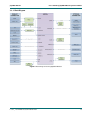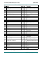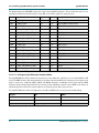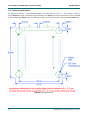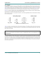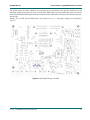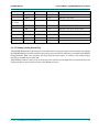
1
phyCORE-AM335x Hardware Manual Document No: L-771e_1 SOM Product No:PCM-051 SOM PCB No:1358.2 Carrier Board Product No:PCM-953 Carrier Board PCB No:1359.2 GPIO Expansion Board Product No: PCM-957 Edition November 2012 A product of a PHYTEC Technology Holding company phyCORE-AM335x In this manual are descriptions for copyrighted products that are not explicitly indicated as such. The absence of the trademark (™), registered trademark (®) and copyright (©) symbols does not imply that a product is not protected. Additionally, registered patents and trademarks are similarly not expressly indicated in this manual. The information in this document has been carefully checked and is believed to be entirely reliable. However, PHYTEC Messtechnik GmbH assumes no responsibility for any inaccuracies. PHYTEC Messtechnik GmbH neither gives any guarantee nor accepts any liability whatsoever for consequential damages resulting from the use of this manual or its associated product. PHYTEC Messtechnik GmbH reserves the right to alter the information contained herein without prior notification and accepts no responsibility for any damages which might result. Additionally, PHYTEC Messtechnik GmbH offers no guarantee nor accepts any liability for damages arising from the improper usage or improper installation of the hardware or software. PHYTEC Messtechnik GmbH further reserves the right to alter the layout and/or design of the hardware without prior notification and accepts no liability for doing so. © Copyright 2012 PHYTEC Messtechnik GmbH, D-55129 Mainz. Rights - including those of translation, reprint, broadcast, photomechanical or similar reproduction and storage or processing in computer systems, in whole or in part - are reserved. No reproduction may occur without the express written consent from PHYTEC Messtechnik GmbH. EUROPE NORTH AMERICA Address: PHYTEC Messtechnik GmbH Robert-Koch-Str. 39 D-55129 Mainz GERMANY PHYTEC America LLC 203 Parfitt Way SW, Suite G100 Bainbridge Island, WA 98110 USA Ordering Information: +49 (6131) 9221-32 [email protected] 1 (800) 278-9913 [email protected] Technical Support: +49 (6131) 9221-31 [email protected] 1 (800) 278-9913 [email protected] Fax: +49 (6131) 9221-33 1 (206) 780-9135 Web Site: www.phytec.de www.phytec.eu www.phytec.com First Edition November 2012 © PHYTEC Messtechnik GmbH 2012 L-771e_1 phyCORE-AM335x Table of content Table of Contents 1 Conventions, Abbreviations and Acronyms .............................................. 1 2 Preface............................................................................................... 4 3 Part I: PCM-051/phyCORE-AM335x System on Module ............................... 8 3.1 Introduction ................................................................................. 8 3.1.1Block Diagram .......................................................................10 3.1.2Component Placement Diagram ................................................11 3.1.3Minimum Requirements to Operate the phyCORE-AM335x...............13 3.2 Pin Description .............................................................................14 3.3 Jumpers......................................................................................25 3.4 Power .........................................................................................30 3.4.1Primary System Power (VDD_5V_IN) ..........................................30 3.4.2Backup Power (VBAT_IN_4RTC).................................................30 3.4.3Power Management IC (U4)......................................................30 3.4.3.1 Power Domains............................................................31 3.4.3.2 Real Time Clock (RTC)....................................................32 3.4.3.3 Power Management ......................................................33 3.4.3.4 External Battery Charging..............................................33 3.4.4Reference Voltages.................................................................33 3.5 Real-Time Clock Options (RTC) .........................................................34 3.5.1PMIC RTC ..............................................................................34 3.5.2External RTC..........................................................................34 3.5.3AM335x RTC ..........................................................................34 3.5.4Power-On Wake .....................................................................34 3.6 System Configuration and Booting ...................................................35 3.7 System Memory ............................................................................37 3.7.1DDR3-SDRAM (U7, U9) ............................................................37 3.7.2NAND Flash Memory (U10) .......................................................37 3.7.2.1 NAND Flash Lock Control (J2) .........................................38 3.7.3I2C EEPROM (U6) ...................................................................38 3.7.3.1 Setting the EEPROM Lower Address Bits (J7, J8).................39 3.7.3.2 EEPROM Write Protection Control (J9) ..............................39 3.7.4SPI Flash Memory (U5) ............................................................40 3.7.4.1 SPI Write-Protect Control (J4) ........................................40 3.7.4.2 SPI Hold Control (J3)....................................................40 3.7.5Memory Model.......................................................................40 L-771e_1 © PHYTEC Messtechnik GmbH 2012 Table of content phyCORE-AM335x 3.8 SD / MMC Card Interfaces................................................................ 41 3.9 Serial Interfaces ........................................................................... 42 3.9.1Universal Asynchronous Receiver/Transmitter Interfaces (UARTs) ... 42 3.9.2USB OTG Interface.................................................................. 43 3.9.3Ethernet Interfaces ................................................................ 44 3.9.3.1 Ethernet1 .................................................................. 44 3.9.3.1.1 Configuring the Ethernet1 Interface Mode ................. 45 3.9.3.2 Ethernet 2.................................................................. 46 3.9.4Profibus............................................................................... 47 3.9.5I2C Interface ........................................................................ 48 3.9.6SPI Interfaces ....................................................................... 48 3.9.7Controller Area Network (CAN) Interfaces ................................... 49 3.9.8Multichannel Audio Serial Ports (McASP) .................................... 50 3.10 General Purpose I/Os..................................................................... 51 3.11 Analog Inputs .............................................................................. 52 3.12 Debug Interface (X2) ..................................................................... 53 3.13 Display Interface .......................................................................... 55 3.13.1Parallel Display Interface....................................................... 55 3.13.2Touch Screen Controller ........................................................ 56 3.14 Technical Specifications ................................................................. 57 3.15 Hints for Integrating and Handling the phyCORE-AM335x ..................... 59 3.15.1Integrating the phyCORE-AM335x ........................................... 59 3.15.2Handling the phyCORE-AM335x .............................................. 61 4 Part II: PCM-953 / phyCORE-AM335x Carrier Board ..................................62 4.1 Introduction................................................................................ 62 4.1.1Concept of the phyCORE-AM335x Carrier Board ............................ 63 4.2 Overview of the phyCORE-AM335x Carrier Board Peripherals .................. 64 4.2.1Connectors and Pin Headers..................................................... 65 4.2.2Switches .............................................................................. 66 4.2.3LEDs ................................................................................... 68 4.2.4Jumpers .............................................................................. 70 4.2.5Carrier Board Bus Enable Decoder ............................................. 75 4.3 Functional Components of the phyCORE-AM335x Carrier Board .............. 78 4.3.1phyCORE-AM335x SOM Connectivity (X1 and X2) .......................... 78 4.3.2Power.................................................................................. 80 4.3.2.1 Wall Adapter Input (X3) ................................................ 81 4.3.2.2 Power Management...................................................... 82 © PHYTEC Messtechnik GmbH 2012 L-771e_1 phyCORE-AM335x Table of content 4.3.2.3 VBAT .........................................................................82 4.3.3Ethernet Connectivity .............................................................82 4.3.3.1 Ethernet 1 (X12)..........................................................83 4.3.3.2 Ethernet 2 (X9)............................................................84 4.3.4EtherCAT (X10 and X11)...........................................................85 4.3.5Profibus (X19).......................................................................86 4.3.6RS-232 (X18) ........................................................................87 4.3.7CAN (X13) ............................................................................88 4.3.8Universal Serial Bus (USB) (X7 and X8).......................................89 4.3.8.1 USB0 (X7) ..................................................................89 4.3.8.2 USB1 (X8) ..................................................................90 4.3.9I2C......................................................................................91 4.3.10SPI (X5) .............................................................................92 4.3.11JTAG (X21)..........................................................................93 4.3.12Display / Touch (X4 and X31) ..................................................94 4.3.12.1PHYTEC Display Interface (PDI) Data Connector (X4) ..........96 4.3.12.2PHYTEC Display Interface (PDI) Power Connector (X31).......99 4.3.12.3AM335x LCD Interface Display (X40) ............................. 100 4.3.12.4Touch Screen Connectivity .......................................... 100 4.3.13Secure Digital Memory (SD) / MultiMedia Card (MMC) Slot (X20) .. 101 4.3.14Audio (X14, X15, X16, X17) .................................................. 102 4.3.15WiFi (X27)......................................................................... 103 5 Part III: PCM-957 GPIO Expansion Board ..............................................106 5.1 GPIO Expansion Board Analog Signals ............................................. 106 5.2 GPIO Expansion Board Control Signals............................................. 107 5.3 GPIO Expansion Board GPIO Signals ................................................ 108 5.4 GPIO Expansion Board GPMC Signals ............................................... 109 5.5 GPIO Expansion Board Power Signals .............................................. 109 5.6 GPIO Expansion Board Serial Interfaces ........................................... 110 5.7 Signals Not Connected to the GPIO Expansion Board .......................... 111 L-771e_1 © PHYTEC Messtechnik GmbH 2012 phyCORE-AM335x List of tables List of Tables Table 1: Abbreviations and Acronyms used in this Manual .................................................. 2 Table 2: Types of Signals ............................................................................................. 3 Table 3: Pinout of the phyCORE-Connector X3, Row A .......................................................16 Table 4: Pinout of the phyCORE-Connector X3, Row B .......................................................18 Table 5: Pinout of the optional phyCORE-Connector X1, Row A ...........................................20 Table 6: Pinout of the optional phyCORE-Connector X1, Row B ...........................................23 Table 7: SOM Jumper Settings .....................................................................................27 Table 8: External Supply Voltages.................................................................................31 Table 9: PMIC Generated Voltages ................................................................................31 Table 10: Power Management Signals .............................................................................33 Table 11: Boot Device Order of AM335x Module ................................................................36 Table 12: NAND GPMC Signal Map...................................................................................37 Table 13: NAND Flash Lock Control via J2.........................................................................38 Table 14: U6 EEPROM I2C Address via J7 and J8 ................................................................39 Table 15: EEPROM Write Protection States Via J9...............................................................39 Table 16: SPI Flash Write-Protection via J4 ......................................................................40 Table 17: SPI Hold Control via J3 ...................................................................................40 Table 18: SD / MMC0 Interface Signal Locations................................................................41 Table 19: UART Signal Locations ....................................................................................42 Table 20: USB OTG Signal Locations................................................................................43 Table 21: Ethernet1 Signal Locations..............................................................................44 Table 22: Ethernet1 TTL Signal Locations.........................................................................45 Table 23: Jumper Configurations for MII and RMII modes ...................................................45 Table 24: Resistor Configurations for MII and RMII modes...................................................46 Table 25: Crystal Configurations for MII and RMII modes ....................................................46 Table 26: Ethernet 2 Signal Locations .............................................................................47 Table 27: Profibus Signal Location Options ......................................................................47 Table 28: I2C Interface Signal Locations..........................................................................48 Table 29: I2C Addresses in Use ......................................................................................48 Table 30: SPI0 Interface Signal Locations ........................................................................48 Table 31: DCAN0 and DCAN1 Signal Locations...................................................................49 Table 32: McASP Signal Locations ..................................................................................50 L-771e_1 © PHYTEC Messtechnik GmbH 2012 phyCORE-AM335x Table 33: Dedicated GPIO Signal Locations ......................................................................51 Table 34: Analog Input Signals......................................................................................52 Table 35: JTAG Connector X2 Signal Assignment ...............................................................54 Table 36: Location of the JTAG Signals on the optional phyCORE-Connector X1 .......................54 Table 37: Parallel Display Interface Signal Locations..........................................................55 Table 38: AIN[3:0] Signal Locations ...............................................................................56 Table 39: phyCORE-AM335x Carrier Board Connectors and Pin Headers ..................................65 Table 40: phyCORE-AM335x Carrier Board push-buttons Descriptions....................................67 Table 41: Carrier Board Boot Configuration Switch S5 ........................................................68 Table 42: phyCORE-AM335x Carrier Board LEDs Descriptions................................................69 Table 43: phyCORE-AM335x Carrier Board Jumper Descriptions............................................72 Table 44: Interfaces Enabled with JP3 and JP4 .................................................................77 Table 45: Bus Switch Enable Status LEDs .........................................................................77 Table 46: Specifically used Pins on the phyCORE-Connector.................................................79 Table 47: VCC_3V3 Jumper Settings................................................................................81 Table 48: Voltage Domains on the Carrier Board................................................................81 Table 49: JP3 and JP4 settings ......................................................................................82 Table 50: JP3 and JP4 settings ......................................................................................86 Table 51: Profibus Jumpers ..........................................................................................87 Table 52: USB Connectors for Different Operating Modes ....................................................90 Table 53: I2C Interface Signals......................................................................................91 Table 54: I2C0 Reserved Addresses.................................................................................92 Table 55: JTAG Connector X1 Pin Descriptions ..................................................................94 Table 56: JP3 and JP4 settings ......................................................................................96 Table 57: PDI Data Connector X4 Signal Description...........................................................97 Table 58: Auxiliary Interfaces at PDI Data Connector X4......................................................98 Table 59: PDI Power Connector X31 Signal Description .......................................................99 Table 60: AM335x LCD Interface Display Connector X40 .................................................... 100 Table 61: Audio Connectors ........................................................................................ 103 Table 62: JP3 and JP4 settings .................................................................................... 104 Table 63: WiFi Module Signals (X27) ............................................................................. 104 Table 64: GPIO Expansion Board Analog Signal Map......................................................... 106 Table 65: GPIO Expansion Board Control Signal Map ........................................................ 107 Table 66: GPIO Expansion Board GPIO Signal Map............................................................ 108 L-771e_1 © PHYTEC Messtechnik GmbH 2012 phyCORE-AM335x Table 67: GPIO Expansion Board GPMC Signal Map ...........................................................109 Table 68: GPIO Expansion Board Power Signal Map ..........................................................109 Table 69: GPIO Expansion Board Serial Interfaces Signal Map ............................................110 Table 70: AM335x SOM Signals Not Routed to the GPIO Expansion Connector X5 ....................111 © PHYTEC Messtechnik GmbH 2012 L-771e_1 phyCORE-AM335x List of figures List of Figures Figure 1: Block Diagram of the phyCORE-AM335x..............................................................10 Figure 2: phyCORE-AM335x Component Placement (top view) .............................................11 Figure 3: phyCORE-AM335x Component Placement (bottom view) ........................................12 Figure 4: Pinout of the phyCORE-Connector (top view, with cross section insert).....................15 Figure 5: Typical Jumper Pad Numbering Scheme..............................................................25 Figure 6: SOM Jumper Locations (top view) .....................................................................26 Figure 7: Power Supply Diagram ....................................................................................32 Figure 8: JTAG Interface at X2 (top view) ........................................................................53 Figure 9: Physical Dimensions.......................................................................................57 Figure 10: Footprint of the phyCORE-AM335x ....................................................................60 Figure 11: phyCORE-AM335x Carrier Board Overview of Connectors and Buttons (top view).........64 Figure 12: Carrier Board Buttons.....................................................................................66 Figure 13: Switch S5 Location ........................................................................................67 Figure 14: Carrier Board LEDs .........................................................................................69 Figure 15: Jumper Numbering Scheme .............................................................................70 Figure 16: Carrier Board Jumper Locations........................................................................71 Figure 17: Bus Enable Jumpers and LEDs ..........................................................................76 Figure 18: phyCORE-AM335x SOM Connectivity to the Carrier Board .......................................78 Figure 19: +5 VDC Power Input Connector .........................................................................80 Figure 20: Ethernet1 Connector ......................................................................................83 Figure 21: Ethernet 2 Connector .....................................................................................84 Figure 22: EtherCAT Connectors ......................................................................................85 Figure 23: Profibus Connector ........................................................................................86 Figure 24: RS-232 Connector..........................................................................................87 Figure 25: CAN Connector and Jumpers ............................................................................88 Figure 26: USB Connectors and Jumpers...........................................................................89 Figure 27: X5 GPIO Expansion Board Connectors ................................................................92 Figure 28: JTAG Connector.............................................................................................93 Figure 29: Display Connectors ........................................................................................95 Figure 30: SD / MMC Connector (X20) ............................................................................ 101 Figure 31: Audio Connectors (X14, X15, X16, X17)............................................................ 102 Figure 32: WiFi Connector............................................................................................ 103 L-771e_1 © PHYTEC Messtechnik GmbH 2012 Conventions, Abbreviations and Acronyms phyCORE-AM335x 1 Conventions, Abbreviations and Acronyms This hardware manual describes the PCM-051 System on Module in the following referred to as phyCORE-AM335x. The manual specifies the phyCORE-AM335x's design and function. Precise specifications for the Texas Instruments AM335x microcontrollers can be found in Texas Instrument's AM335x Data Sheet and Technical Reference Manual. Note: We refrain from providing detailed part specific information within this manual, which can be subject to continuous changes, due to part maintenance for our products. Please read the paragraph "Product Change Management and information in this manual on parts populated on the SOM" within the Section 2. Note: The BSP delivered with the phyCORE-AM335x usually includes drivers and/or software for controlling all components such as interfaces, memory, etc.. Therefore programming close to hardware at register level is not necessary in most cases. For this reason, this manual contains no detailed description of the controller's registers, or information relevant for software development. Please refer to the AM335x Reference Manual, if such information is needed to connect customer designed applications. Conventions The conventions used in this manual are as follows: • Signals that are preceded by a "n", "/", or “#” character (e.g.: nRD, /RD, or #RD), or that have a dash on top of the signal name (e.g.: RD) are designated as active low signals. That is, their active state is when they are driven low, or are driving low. • A "0" indicates a logic zero or low-level signal, while a "1" represents a logic one or high-level signal. • The hex-numbers given for addresses of I2C devices always represent the 7 MSB of the address byte. The correct value of the LSB which depends on the desired command (read (1), or write (0)) must be added to get the complete address byte. E.g. given address in this manual 0x41 => complete address byte = 0x83 to read from the device and 0x82 to write to the device • Tables which describe jumper settings show the default position in bold, blue text • Text in blue italic indicates a hyperlink within, or external to the document. Click these links to quickly jump to the applicable URL, part, chapter, table, or figure. • References made to the phyCORE-Connector always refer to the high density Samtec connectors on the undersides of the phyCORE-AM335x 1 © PHYTEC Messtechnik GmbH 2012 L-771e_1 phyCORE-AM335x Conventions, Abbreviations and Acronyms Abbreviations and Acronyms Many acronyms and abbreviations are used throughout this manual. Use the table below to navigate unfamiliar terms used in this document. Abbreviation Definition BSP Board Support Package (Software delivered with the Development Kit including an operating system (Windows or Linux) preinstalled on the module and Development Tools). CB Carrier Board; used in reference to the phyCORE-AM335x Development Kit Carrier Board. DFF D flip-flop EMB External memory bus EMI Electromagnetic interference GPI General purpose input GPIO General purpose input and output GPO General purpose output IRAM Internal RAM; the internal static RAM on the Texas Instruments AM335x microcontroller J Solder jumper; these types of jumpers require solder equipment to remove and place JP Solderless jumper; these types of jumpers can be removed and placed by hand with no special tools PCB Printed circuit board PDI PHYTEC Display Interface; defined to connect PHYTEC display adapter boards, or custom adapters PEB PHYTEC Extension Board PMIC Power management IC PoE Power over Ethernet PoP Package on Package POR Power-on reset RTC Real-time clock SMT Surface mount technology SOM System on Module; used in reference to the PCM-051 / phyCORE-AM335x System on Module Sx User button Sx (e.g. S1, S2, etc.) used in reference to the available user buttons, or DIP switches on the carrier board Sx_y Switch y of DIP switch Sx; used in reference to the DIP switch on the carrier board VBAT SOM standby voltage input Table 1: Abbreviations and Acronyms used in this Manual L-771e_1 © PHYTEC Messtechnik GmbH 2012 2 Conventions, Abbreviations and Acronyms phyCORE-AM335x Different types of signals are brought out at the phyCORE-Connector. The following table lists the abbreviations used to specify the type of a signal. Type of Signal Description Abbr. Power Supply voltage PWR Ref-Voltage Reference voltage REF USB-Power USB voltage USB Input Digital input IN Output Digital output OUT Input with pull-up Input with pull-up, must only be connected to GND (jumper or open-collector output). IPU Input / output Bidirectional input / output IO 5 V Input with pull-down 5 V tolerant input with pull-down 5V_PD 5 V Input with pull-up 5 V tolerant input with pull-up 5V_PU LVDS Differential line pairs 100 Ohm LVDS Pegel LVDS Differential 90 Ohm Differential line pairs 90 Ohm DIFF90 Differential 100 Ohm Differential line pairs 100 Ohm DIFF100 Analog Analog input or output Analog Table 2: Types of Signals 3 © PHYTEC Messtechnik GmbH 2012 L-771e_1 phyCORE-AM335x Preface 2 Preface As a member of PHYTEC's phyCORE product family the phyCORE-AM335x is one of a series of PHYTEC System on Modules (SOMs) that can be populated with different controllers and, hence, offers various functions and configurations. PHYTEC supports a variety of 8-/16- and 32-bit controllers in two ways: 1. as the basis for Rapid Development Kits which serve as a reference and evaluation platform 2. as insert-ready, fully functional phyCORE OEM modules, which can be embedded directly into the user’s peripheral hardware design Implementation of an OEM-able SOM subassembly as the "core" of your embedded design allows you to focus on hardware peripherals and firmware without expending resources to "re-invent" microcontroller circuitry. Furthermore, much of the value of the phyCORE module lies in its layout and test. Production-ready Board Support Packages (BSPs) and Design Services for our hardware will further reduce your development time and risk and allow you to focus on your product expertise. Take advantage of PHYTEC products to shorten time-to-market, reduce development costs, and avoid substantial design issues and risks. With this new innovative full system solution you will be able to bring your new ideas to market in the most timely and cost-efficient manner. For more information go to: www.phytec.de/de/leistungen/entwicklungsunterstuetzung.html, or www.phytec.eu/europe/oem-integration/evaluation-start-up.html L-771e_1 © PHYTEC Messtechnik GmbH 2012 4 Preface phyCORE-AM335x Ordering Information The part numbering of the phyCORE has the following structure1: 1. The structure shows the ordering options available as of the printing of this manual. Additional ordering options may have been added. Please contact our sales team to ´get an update on the ordering options available. 5 © PHYTEC Messtechnik GmbH 2012 L-771e_1 phyCORE-AM335x Preface In order to receive product specific information on changes and updates in the best way also in the future, we recommend to register at www.phytec.de/de/support/registrierung.html, or www.phytec.eu/europe/support/registration.html For technical support and additional information concerning your product, please visit the support section of our web site which provides product specific information, such as errata sheets, application notes, FAQs, etc. www.phytec.de/de/support/faq/faq-phycore-AM335x.html, or www.phytec.eu/europe/support/faq/faq-phycore-AM335x.html Declaration of Electro Magnetic Conformity of the PHYTEC phyCORE-AM335x PHYTEC System on Modules (henceforth products) are designed for installation in electrical appliances or as dedicated Evaluation Boards (i.e.: for use as a test and prototype platform for hardware/software development) in laboratory environments. Caution: PHYTEC products lacking protective enclosures are subject to damage by ESD and, hence, may only be unpacked, handled or operated in environments in which sufficient precautionary measures have been taken in respect to ESD-dangers. It is also necessary that only appropriately trained personnel (such as electricians, technicians and engineers) handle and/or operate these products. Moreover, PHYTEC products should not be operated without protection circuitry if connections to the product's pin header rows are longer than 3 m. PHYTEC products fulfill the norms of the European Union’s Directive for Electro Magnetic Conformity only in accordance to the descriptions and rules of usage indicated in this hardware manual (particularly in respect to the pin header row connectors, power connector and serial interface to a host-PC). Caution: Implementation of PHYTEC products into target devices, as well as user modifications and extensions of PHYTEC products, is subject to renewed establishment of conformity to, and certification of, Electro Magnetic Directives. Users should ensure conformance following any modifications to the products as well as implementation of the products into target systems. L-771e_1 © PHYTEC Messtechnik GmbH 2012 6 Preface phyCORE-AM335x Product Change Management and information in this manual on parts populated on the SOM When buying a PHYTEC SOM, you will, in addition to our HW and SW offerings, receive a free obsolescence maintenance service for the HW we provide. Our PCM (Product Change Management) Team of developers is continuously processing all incoming PCN's (Product Change Notifications) from vendors and distributors concerning parts which are being used in our products. Possible impacts to the functionality of our products, due to changes of functionality or obsolesce of a certain part, are being evaluated in order to take the right masseurs in purchasing or within our HW/SW design. Our general philosophy here is: We never discontinue a product as long as there is demand for it. Therefore we have established a set of methods to fulfill our philosophy: Avoiding strategies • Avoid changes by evaluating long-livety of a parts during design in phase • Ensure availability of equivalent second source parts • Stay in close contact with part vendors to be aware of roadmap strategies Change management in case of functional changes • Avoid impacts on Product functionality by choosing equivalent replacement parts • Avoid impacts on Product functionality by compensating changes through HW redesign or backward compatible SW maintenance • Provide early change notifications concerning functional relevant changes of our Products Change management in rare event of an obsolete and non replaceable part • Ensure long term availability by stocking parts through last time buy management according to product forecasts • Offer long term frame contract to customers Therefore we refrain from providing detailed part specific information within this manual, which can be subject to continuos changes, due to part maintenance for our products. In order to receive reliable, detailed and up-to-date information concerning parts used for our product, please contact our support team for through the given contact information within this manual. 7 © PHYTEC Messtechnik GmbH 2012 L-771e_1 phyCORE-AM335x Part I: PCM-051/phyCORE-AM335x System on Module 3 Part I: PCM-051/phyCORE-AM335x System on Module Part I of this three part manual provides detailed information on the phyCORE-AM335x System on Module (SOM) designed for custom integration into customer applications. The information in the following chapters is applicable to the 1358.2 PCB revision of the phyCORE-AM335x SOM. 3.1 Introduction The phyCORE-AM335x belongs to PHYTEC’s phyCORE System on Module family. The phyCORE SOMs represent the continuous development of PHYTEC System on Module technology. Like its mini-, micro- and nanoMODUL predecessors, the phyCORE boards integrate all core elements of a microcontroller system on a subminiature board and are designed in a manner that ensures their easy expansion and embedding in peripheral hardware developments. As independent research indicates that approximately 70% of all EMI (Electro Magnetic Interference) problems stem from insufficient supply voltage grounding of electronic components in high frequency environments, the phyCORE board design features an increased pin package. The increased pin package allows dedication of approximately 20% of all connector pins on the phyCORE boards to ground. This improves EMI and EMC characteristics and makes it easier to design complex applications meeting EMI and EMC guidelines using phyCORE boards even in high noise environments. phyCORE boards achieve their small size through modern SMD technology and multi-layer design. In accordance with the complexity of the module, 0402-packaged SMD components and laser-drilled microvias are used on the boards, providing phyCORE users with access to this cutting edge miniaturization technology for integration into their own design. The phyCORE-AM335x is a subminiature (44 mm x 50 mm) insert-ready System on Module populated with the Texas Instruments AM335x microcontroller. Its universal design enables its insertion in a wide range of embedded applications. All controller signals and ports extend from the controller to high-density pitch (0.5 mm) connectors aligning two sides of the board, allowing it to be plugged like a "big chip" into a target application. Precise specifications for the controller populating the board can be found in the applicable controller Technical Reference Manual or datasheet. The descriptions in this manual are based on the Texas Instruments AM335x. No description of compatible microcontroller derivative functions is included, as such functions are not relevant for the basic functioning of the phyCORE-AM335x. The phyCORE-AM335x offers the following features: • Insert-ready, sub-miniature (44 mm x 50 mm) System on Module (SOM) subassembly in low EMI design, achieved through advanced SMD technology • Populated with the Texas Instruments AM335x microcontroller (ZCZ 324-pin PBGA package) • Max. 720 MHz core clock frequency • Boot from NAND Flash or SPI Flash • Controller signals and ports extend to two high-density (0.5 mm) Samtec connectors aligning two sides of the board, enabling it to be plugged like a "big chip" into target application • Single supply voltage of 5 V (max. 600 mA) with on-board power management • All controller required supplies generated on board • Improved interference safety achieved through multi-layer PCB technology and dedicated ground pins L-771e_1 © PHYTEC Messtechnik GmbH 2012 8 Part I: PCM-051/phyCORE-AM335x System on Module phyCORE-AM335x • General-Purpose Memory Controller Bus (GPMC): flexible 8/16-bit asynchronous memory interface with up to 7 chip-select signals. • 128 MB (up to 512 MB) on-board NAND Flash1 • 8 MB (up to 32 MB) on-board SPI Flash1 • 256 MB (up to 1 GB) DDR3 SDRAM1 • 4 kB (up to 32 kB) I2C EEPROM1 • One serial interface (TTL) • Two High-Speed USB OTG interfaces • One 10/100 MBit Ethernet interface. Either with Ethernet transceiver on the phyCORE-AM335x allowing for direct connection to an existing Ethernet network, or without on-board transceiver and provision of the RMII signals at TTL-level at the phyCORE-Connector instead2 • One 10/100/1000 RGMII Ethernet interface. The TTL-level inteface is available at the optional phyCORE connector. • One I2C interface • One SPI interface • Up to two CAN interfaces • LCD Interface Display Driver with an integrated touch interface and up to 24 data bits • Up to two multichannel audio serial interfaces (McASP) • Support of standard 20 pin debug interface through JTAG connector2 • One SD/MMC card interfaces • On-board power management IC with integrated RTC • Real-Time Clock2 Caution: Samtec connectors guarantee optimal connection and proper insertion of the phyCORE-AM335x. Please make sure that the phyCORE-AM335x is fully plugged into the matting connectors of the carrier board. Otherwise individual signals may have bad, or no contact. 1. 2. 9 The maximum memory size listed is as of the printing of this manual. Please contact PHYTEC for more information about additional, or new module configurations available. Please refer to the order options described in the Preface, or contact PHYTEC for more information about additional module configurations. © PHYTEC Messtechnik GmbH 2012 L-771e_1 phyCORE-AM335x Part I: PCM-051/phyCORE-AM335x System on Module 3.1.1 Block Diagram Figure 1: Block Diagram of the phyCORE-AM335x L-771e_1 © PHYTEC Messtechnik GmbH 2012 10 Part I: PCM-051/phyCORE-AM335x System on Module phyCORE-AM335x 3.1.2 Component Placement Diagram Figure 2: phyCORE-AM335x Component Placement (top view) 11 © PHYTEC Messtechnik GmbH 2012 L-771e_1 phyCORE-AM335x Part I: PCM-051/phyCORE-AM335x System on Module Figure 3: phyCORE-AM335x Component Placement (bottom view) L-771e_1 © PHYTEC Messtechnik GmbH 2012 12 Part I: PCM-051/phyCORE-AM335x System on Module phyCORE-AM335x 3.1.3 Minimum Requirements to Operate the phyCORE-AM335x Basic operation of the phyCORE-AM335x requires only supply of a +5.0 V input voltage with minimum 2.0 A capacity and the corresponding GND connections. These supply pins are located at the phyCORE-Connector X3: VCC_5V0: Connector: X3 Pins: 1B, 2B, 3B, 5B Connect all 5 V input pins to your power supply and at least the matching number of GND pins. Corresponding GND: Connector: X3 Pins: 1A, 4A, 8A, 4B, 7B Please refer to Section 3.2 for information on additional GND Pins located at the phyCORE-Connector X3. Caution: We recommend connecting all available 5 V input pins to the power supply system on a custom carrier board housing the phyCORE-AM335x and at least the matching number of GND pins neighboring the 5 V pins. In addition, proper implementation of the phyCORE-AM335x module into a target application also requires connecting all GND pins neighboring signals that are being used in the application circuitry. Please refer to Section 3.4 for more information. 13 © PHYTEC Messtechnik GmbH 2012 L-771e_1 phyCORE-AM335x Part I: PCM-051/phyCORE-AM335x System on Module 3.2 Pin Description Please note that all module connections are not to exceed their expressed maximum voltage or current. Maximum signal input values are indicated in the corresponding controller manuals/data sheets. As damage from improper connections varies according to use and application, it is the user's responsibility to take appropriate safety measures to ensure that the module connections are protected from overloading through connected peripherals. All controller signals extend to surface mount technology (SMT) connectors (0.5 mm) lining two sides of the module (referred to as the phyCORE-Connector). This allows the phyCORE-AM335x to be plugged into any target application like a "big chip". The numbering scheme for the phyCORE-Connector is based on a two dimensional matrix in which column positions are identified by a letter and row position by a number. Pin A1, for example, is located in the upper left hand corner of the matrix looking down through the top of the SOM. The pin numbering values increase moving down on the board. Lettering of the pin connector rows progresses alphabetically from left to right for each connector (refer to Figure 4 ). The numbered matrix can be aligned with the phyCORE-AM335x (viewed from above; phyCORE-Connector pointing down) or with the socket of the corresponding phyCORE Carrier Board/user target circuitry. The upper left-hand corner of the numbered matrix (pin 1A) is thus covered with the corner of the phyCORE-AM335x marked with a triangle. The numbering scheme is always in relation to the PCB as viewed from above, even if all connector contacts extend to the bottom of the module. The numbering scheme is thus consistent for both the module’s phyCORE-Connector as well as the mating connector on the phyCORE-AM335x Carrier Board or target hardware, thereby considerably reducing the risk of pin identification errors. Since the pins are exactly defined according to the numbered matrix previously described, the phyCOREConnector is usually assigned a single designator for its position (X1 for example). In this manner the phyCOREConnector comprises a single, logical unit regardless of the fact that it could consist of more than one physical socketed connector. The following figure illustrates the numbered matrix system. It shows a phyCORE-AM335x with SMT phyCOREConnectors on its underside (defined with dotted lines) mounted on a carrier board. In order to facilitate understanding of the pin assignment scheme, the diagram presents a cross-view of the phyCORE-module showing these phyCORE-Connectors mounted on the underside of the module’s PCB. L-771e_1 © PHYTEC Messtechnik GmbH 2012 14 Part I: PCM-051/phyCORE-AM335x System on Module phyCORE-AM335x Figure 4: Pinout of the phyCORE-Connector (top view, with cross section insert) Table 3 provides an overview of the pinout of the phyCORE-Connector with signal names and descriptions specific to the phyCORE-AM335x. It also provides the appropriate signal level interface voltages listed in the SL (Signal Level) column and the signal direction. Caution: Most of the controller pins have multiple multiplexed functions. Because most of these pins are connected directly to the phyCORE-Connector the functions are also available there. Signal names and descriptions in Table 3 however, are in regard to the specification of the phyCORE-AM335x and the functions defined therein. Please refer to the AM335x datasheet, or the schematic to to get to know about alternative functions. In order to utilize a specific pin's alternative function the corresponding registers must be configured within the appropriate driver of the BSP. To support all features of the phyCORE-AM335x Carrier Board a few changes have been made in the BSP delivered with the module. Table 33 lists all pins with functions different from what is described in Table 3. The Texas Instruments AM335x is a multi-voltage operated microcontroller and as such special attention should be paid to the interface voltage levels to avoid unintentional damage to the microcontroller and other on-board components. Please refer to the Texas Instruments AM335x Reference Manual for details on the functions and features of controller signals and port pins. Note: SL is short for Signal Level (V) and is the applicable logic level to interface a given pin. 15 © PHYTEC Messtechnik GmbH 2012 L-771e_1 phyCORE-AM335x Part I: PCM-051/phyCORE-AM335x System on Module Pin Row X3A Pin # Signal Type SL Description 1A GND - - Ground 0 V 2A VBAT_IN_4RTC PWR 3V-5V Optional always-on power for the Real-Time Clock (RTC). If a backup batter is not used, connect this pin to the primary 5V supply. 3A VDIG1_1P8V REF 1.8 V 1.8 V reference voltage out 4A GND - - Ground 0 V 5A X_AM335_NMIn IPU 3.3 V Non-maskable interrupt to the AM335x processor 6A X_ETH1_RXn IO 3.3 V Ethernet PHY data minus 7A X_ETH1_RXp IO 3.3 V Ethernet PHY data plus 8A GND - - Ground 0 V 9A X_ETH1_TXn IO 3.3 V Ethernet PHY data minus 10A X_ETH1_TXp IO 3.3 V Ethernet PHY data plus 11A X_PB_RESETn IN 3.3 V Push-button reset 12A GND - - Ground 0 V 13A X_ETH_LED2 / INTSELn IO 3.3 V Ethernet configuration input and speed LED control output. For Ethernet configuration, this signal should be pulled HIGH until system reset is deasserted. 14A X_ETH_LED1 / REGOFF IO 3.3 V Ethernet configuration input and activity LED control output. For Ethernet configuration, this signal should be pulled LOW until system reset is deasserted. 15A X_SPI0_SCLK OUT 3.3 V Serial Peripheral Interface 0 clock. 16A GND - - Ground 0 V 17A X_SPI0_CS0 OUT 3.3 V Serial Peripheral Interface 0 chip select 0. This signal is not externally available in the default SOM configuration as it connectes to a SPI Flash. 18A X_SPI0_CS1 / MMC0_SDCD IO 3.3 V Serial Peripheral Interface 0 chip select 1 or MMC/SD0 Card Detect 19A X_I2C0_SCL IO 3.3 V I²C bus 0 clock. Some I2C0 address are reserved. See Section 3.9.5 20A X_I2C0_SDA IO 3.3 V I²C bus 0 data. 21A GND - - Ground 0 V 22A X_MCASP0_AXR0 IO 3.3 V Multi-channel Audio Serial Port 0 data 0 23A X_GPIO_3_17 IO 3.3 V AM335x GPIO3_17 Table 3: Pinout of the phyCORE-Connector X3, Row A L-771e_1 © PHYTEC Messtechnik GmbH 2012 16 Part I: PCM-051/phyCORE-AM335x System on Module phyCORE-AM335x Pin Row X3A Pin # Signal Type SL Description 24A X_MII1_TXD2 IN 3.3 V Ethernet 1 MII transmit data 25A X_MII1_TXD3 OUT 3.3 V Ethernet 1 MII transmit data 26A GND - - Ground 0 V 27A X_MCASP0_AHCLKX IO 3.3 V Multi-channel Audio Serial Port 0 Tx bit clock 28A X_MCASP0_AXR1 IO 3.3 V Multi-channel Audio Serial Port 0 data 1 29A X_MCASP0_FSX IO 3.3 V Multi-channel Audio Serial Port 0 Tx frame sync 30A X_PORZ OUT 3.3 V Power-on reset (low-true) 31A GND - - Ground 0 V 32A X_UART0_TXD OUT 3.3 V UART0 Tx data from AM335x 33A X_UART0_RXD IN 3.3 V UART0 Rx data to AM335x 34A X_SPI0_D0 IN 3.3 V Serial Peripheral Interface 0 Master-In-SlaveOut (MISO) data 35A X_SPI0_D1 OUT 3.3 V Serial Peripheral Interface 0 Master-Out-SlaveIn (MOSI) data 36A GND - - Ground 0 V 37A X_LCD_D3 / P_MII0_TXD2 IO 3.3 V LCD data 3 or PRU Ethernet 0 Tx data 2 38A X_LCD_D2 / P_MII0_TXD3 IO 3.3 V LCD data 2 or PRU Ethernet 0 Tx data 3 39A X_LCD_D4 / P_MII0_TXD1 IO 3.3 V LCD data 4 or PRU Ethernet 0 Tx data 1 40A X_LCD_D5 / P_MII0_TXD0 IO 3.3 V LCD data 5 or PRU Ethernet 0 Tx data 0 41A GND - - Ground 0 V 42A X_LCD_D0 / P_MII0_MT_CLK IO 3.3 V LCD data 0 or PRU Ethernet 0 Tx clock 43A X_LCD_D1 / P_MII0_TXEN OUT 3.3 V LCD data 1 or PRU Ethernet 0 Tx enable 44A X_LCD_D13 / P_MII0_RXER IO 3.3 V LCD data 13 or PRU Ethernet 0 Rx error 45A X_LCD_HSYNC OUT 3.3 V LCD horizontal sync 46A GND - - Ground 0 V 47A X_USB0_DM DIFF1 3.3 V 00 USB 0 data minus 48A X_USB0_DP DIFF1 3.3 V 00 USB 0 data plus 49A X_LCD_D12 / P_MII0_RXLINK IO 3.3 V LCD data 12 or PRU Ethernet 0 Rx link 50A X_LCD_BIAS_EN / P_MII1_CRS IO 3.3 V LCD AC bias enable or PRU Ethernet 1 carrier sense 51A GND - - Ground 0 V 52A X_LCD_D8 / P_MII0_RXD3 IO 3.3 V LCD data 8 or PRU Ethernet 0 Rx data 3 Table 3: Pinout of the phyCORE-Connector X3, Row A 17 © PHYTEC Messtechnik GmbH 2012 L-771e_1 phyCORE-AM335x Part I: PCM-051/phyCORE-AM335x System on Module Pin Row X3A Pin # Signal 53A Type SL Description X_LCD_D14 / P_MII0_MR_CLK IO 3.3 V LCD data 14 or PRU Ethernet 0 Rx clock 54A X_LCD_D15 / P_MII0_RXDV IO 3.3 V LCD data 15 or PRU Ethernet Rx data valid 55A X_LCD_D6 OUT 3.3 V LCD data 56A GND - - Ground 0 V 57A X_LCD_D7 OUT 3.3 V LCD data 58A X_LCD_D9 / P_MII0_RXD2 IO 3.3 V LCD data 9 or PRU Ethernet 0 Rx data 2 59A X_LCD_D10 / P_MII0_RXD1 IO 3.3 V LCD data 10 or PRU Ethernet 0 Rx data 1 60A X_UART2_RX IN 3.3 V UART 2 Rx data to AM335x Table 3: Pinout of the phyCORE-Connector X3, Row A Pin Row X3B Pin # Signal Type SL Description 1B VDD_5V_IN PWR 5.0 V 3.6 V - 5 V power input 2B VDD_5V_IN PWR 5.0 V 3.6 V - 5 V power input 3B VDD_5V_IN PWR 5.0 V 3.6 V - 5 V power input 4B GND - - Ground 0 V 5B VDD_5V_IN PWR 5.0 V 3.6 V - 5 V power input 6B VAUX2_3P3V REF 3.3 V 3.3 V reference Voltage 7B GND - - Ground 0 V 8B X_UART1_CTS IN 3.3 V UART1 clear to send 9B X_UART1_RTS OUT 3.3 V UART1 ready to send 10B X_UART1_TX / P_UART0_TX OUT 3.3 V UART 1 Tx data or PRU UART0 Tx data 11B X_UART1_RX / P_UART0_RX IN 3.3 V UART 1 Rx data or PRU UART0 Rx data 12B GND - - Ground 0 V 13B X_RESET_OUTn OUT 3.3 V Reset output 14B X_PB_POWER IN 5.0 V Push-button power control. Behavior is configurable. See Section 3.4.3.3 15B GPIO_3_19 IO 3.3 V AM335x GPIO_3_19 16B X_MCASP0_ACLKX IO 3.3 V Multi-channel Audio Serial Port 0 Tx bit clock 17B GND - - Ground 0 V 18B X_USB1_DP DIFF10 3.3 V 0 USB 1 data plus 19B X_USB1_DM DIFF10 3.3 V 0 USB 1 data minus Table 4: Pinout of the phyCORE-Connector X3, Row B L-771e_1 © PHYTEC Messtechnik GmbH 2012 18 Part I: PCM-051/phyCORE-AM335x System on Module phyCORE-AM335x Pin Row X3B Pin # Signal Type SL Description 20B GND - - Ground 0 V 21B X_USB1_DRVVBUS OUT 3.3 V USB 1 VBUS control output 22B X_USB1_VBUS USB 5.0 V USB 1 bus voltage 23B X_USB1_ID IN 1.8 V USB 1 port identification. 1.8 V logic. 24B X_USB1_CE OUT 3.3 V USB 1 port charger enable 25B GND - - Ground 0 V 26B X_ECAP0_IN_PWM0_OUT IO 3.3 V Enhanced Capture 0 input or Auxiliary Pulse-Width Modulated 0 output 27B GNDA_ADC - - Analog Ground 0 V 28B X_AIN7 analog 1.8 V AM335x analog input 7 29B X_AIN6 analog 1.8 V AM335x analog input 6 30B GNDA_ADC - Analog Ground 0 V 31B X_AIN5 analog 1.8 V AM335x analog input 5 32B X_AIN4 analog 1.8 V AM335x analog input 4 33B GNDA_ADC - Analog Ground 0 V 34B X_AIN2 analog 1.8 V AM335x analog input 2 / Touch Y+ 35B X_AIN3 analog 1.8 V AM335x analog input 3 / Touch Y- 36B GNDA_ADC - Analog Ground 0 V 37B X_AIN1 analog 1.8 V AM335x analog input 1 / Touch X- 38B X_AIN0 analog 1.8 V AM335x analog input 0 / Touch X+ 39B X_AM335_EXT_WAKEUP IN 1.8 V AM335x processor external wakeup 40B GND - - Ground 0 V 41B X_USB0_VBUS IN 5.0 V USB 0 bus voltage 42B X_USB0_DRVVBUS OUT 3.3 V USB 0 VBUS control output 43B X_USB0_ID IN 1.8 V USB 0 port identification. 1.8 V logic 44B X_USB0_CE OUT 3.3 V USB 0 charger enable 45B GND - - Ground 0 V 46B X_LCD_PCLK / P_MII0_CRS IO 3.3 V LCD pixel clock or PRU Ethernet 0 carrier sense 47B X_LCD_VSYNC OUT 3.3 V LCD vertical sync 48B GND - - Ground 0 V 49B X_LCD_D11 / P_MII0_RXD0 IO 3.3 V LCD data 11 or PRU Ethernet 0 Rx data 0 50B X_GPIO_1_9 IO 3.3 V AM335x GPIO_1_9 51B X_GPIO_1_8 IO 3.3 V AM335x GPIO_1_8 - - - Table 4: Pinout of the phyCORE-Connector X3, Row B 19 © PHYTEC Messtechnik GmbH 2012 L-771e_1 phyCORE-AM335x Part I: PCM-051/phyCORE-AM335x System on Module Pin Row X3B Pin # Signal Type SL Description 52B GND - - Ground 0 V 53B X_MMC0_CLK IO 3.3 V MMC / SDIO 0 clock 54B X_MMC0_CMD IO 3.3 V MMC / SDIO 0 command 55B X_MMC0_D0 IO 3.3 V MMC / SDIO 0 data 0 56B X_MMC0_D1 IO 3.3 V MMC / SDIO 0 data 1 57B GND - - Ground 0 V 58B X_MMC0_D2 IO 3.3 V MMC / SDIO 0 data 2 59B X_MMC0_D3 IO 3.3 V MMC / SDIO 0 data 3 60B X_UART2_TX OUT 3.3 V UART 2 Tx data to Carrier Board Table 4: Pinout of the phyCORE-Connector X3, Row B Pin Row X1A (Optional Connector) Pin # Signal Type SL Description 1A X_RMII_RXER / MCASP1_FSX IO 3.3 V Ethernet1 RMII Rx error or Multichannel Audio Serial Port1 Tx frame sync 2A GND - - Ground 0 V 3A X_RMII1_RXD0 / GPIO_2_21 IO 3.3 V Ethernet1 RMII Rx data 0 or AM335x GPIO_2_21 4A X_RMII1_RXD1 / GPIO_2_20 IO 3.3 V Ethernet1 RMII Rx data 1 or AM335x GPIO_2_20 5A - - - Reserved, no-connect 6A - - - Reserved, no-connect 7A GND - - Ground 0 V 8A X_UART3_RX IN 3.3 V UART3 Rx data 9A X_UART3_TX OUT 3.3 V UART3 Tx data 10A X_RMII1_TXEN / MCASP1_AXR0 IO 3.3 V Ethernet1 RMII Tx enable or Multichannel Audio Serial Port 1 data 0 11A X_RMII1_TXD0 / GPIO_0_28 IO 3.3 V Ethernet1 RMII Tx data 0 or AM335x GPIO_0_28 12A GND - - Ground 0 V 13A X_RMII1_TXD1 / GPIO_0_21 IO 3.3 V Ethernet1 RMII Tx data 1 or AM335x GPIO_0_21 14A X_MII1_COL / MCASP1_AXR2 IO 3.3 V Ethernet1 MII collision detect or Multichannel Audio Serial Port 1 data 2 Table 5: Pinout of the optional phyCORE-Connector X1, Row A L-771e_1 © PHYTEC Messtechnik GmbH 2012 20 Part I: PCM-051/phyCORE-AM335x System on Module phyCORE-AM335x Pin Row X1A (Optional Connector) Pin # Signal Type SL Description 15A X_RMII1_CRS / MCASP1_ACLKX IO 3.3 V Ethernet1 RMII carrier sense or Multichannel Audio Serial Port 1 Tx bit clock 16A X_GPMC_AD1 IO 3.3 V General Purpose Memory Controller interface Address/Data 17A GND - - Ground 0 V 18A RMII1_REFCLK / GPIO_0_29 IO 3.3 V Ethernet1 RMII reference clock 19A - - - Reserved, no-connect 20A - - - Reserved, no-connect 21A - - - Reserved, no-connect 22A GND - - Ground 0 V 23A X_GPMC_AD0 IO 3.3 V General Purpose Memory Controller interface Address/Data 24A X_GPMC_AD2 IO 3.3 V General Purpose Memory Controller interface Address/Data 25A X_GPMC_AD4 IO 3.3 V General Purpose Memory Controller interface Address/Data 26A X_GPMC_AD5 IO 3.3 V General Purpose Memory Controller interface Address/Data 27A GND - - Ground 0 V 28A X_GPMC_AD3 IO 3.3 V General Purpose Memory Controller interface Address/Data 29A X_GPMC_AD6 IO 3.3 V General Purpose Memory Controller interface Address/Data 30A X_GPMC_AD7 IO 3.3 V General Purpose Memory Controller interface Address/Data 31A - - - Reserved, no-connect 32A GND - - Ground 0 V 33A X_GPMC_ADVn_ALE OUT 3.3 V General Purpose Memory Controller interface address valid / address latch enable 34A X_GPMC_BE0n_CLE OUT 3.3 V General Purpose Memory Controller interface byte enable 0 / command latch enable 35A X_RGMII2_RCTL / MMC2_DAT0 / P_MII1_TXD3 IO 3.3 V Ethernet 2 RGMII Rx control or MMC/ SDIO 2 data 2 or PRU Ethernet1 Tx data 3 Table 5: Pinout of the optional phyCORE-Connector X1, Row A 21 © PHYTEC Messtechnik GmbH 2012 L-771e_1 phyCORE-AM335x Part I: PCM-051/phyCORE-AM335x System on Module Pin Row X1A (Optional Connector) Pin # Signal Type SL Description 36A X_RGMII2_TD3 / MMC2_DAT1 / P_MII1_TXD2 IO 3.3 V Ethernet 2 RGMII Tx data 3 or MMC/SDIO 2 data 1 or PRU Ethernet1 Tx data 2 37A GND - - Ground 0 V 38A X_RMII2_CRS_DV IO 3.3 V Ethernet 2 RMII CRS/DV signal. This signal can replace the NAND Ready/Busy signal to AM335x pin T17. See section Section 3.9.3.2 39A X_RGMII2_TD2 / MMC2_DAT2 / P_MII1_TXD1 IO 3.3 V Ethernet 2 RGMII Tx data 2 or MMC/SDIO 2 data 2 or PRU Ethernet1 Tx data 1 40A X_RGMII2_TD0 / P_MII1_RXD3 IO 3.3 V Ethernet 2 RGMII Tx data 0 or PRU Ethernet1 Rx data 3 41A X_RGMII2_TCLK / MMC2_DAT4 / P_MII1_RXD2 IO 3.3 V Ethernet 2 RGMII transmit clock or MMC2 data 4 or PRU Ethernet1 Rx data 2 42A GND - - Ground 0 V 43A X_RGMII2_RCLK / MMC2_DAT5 / P_MII1_RXD1 IO 3.3 V Ethernet 2 RGMII Rx clock or MMC/ SDIO 2 data 5 or PRU Ethernet1 Rx data 1 44A X_RGMII2_RD2 / MMC2_DAT7 / P_MII1_MR1_CLK IO 3.3 V Ethernet 2 RGMII Rx data 2 or MMC/ SDIO 2 data 7 or PRU Ethernet1 Rx clock 45A X_RGMII2_RD1 / P_MII1_RXDV IO 3.3 V Ethernet 2 RGMII Rx data 1 or PRU Ethernet1 Rx data valid 46A X_RGMII2_RD0 / P_MII1_RXER IO 3.3 V Ethernet 2 RGMII Rx data 0 or PRU Ethernet1 Rx error 47A GND - - Ground 0 V 48A X_MMC2_CLK / P_MDIO_MDCLK IO 3.3 V MMC/SDIO 2 clock or PRU Ethernet1 MDIO clock 49A - - - Reserved, no-connect 50A - - - Reserved, no-connect Table 5: Pinout of the optional phyCORE-Connector X1, Row A L-771e_1 © PHYTEC Messtechnik GmbH 2012 22 Part I: PCM-051/phyCORE-AM335x System on Module phyCORE-AM335x Pin Row X1B (Optional Connector) Pin # Signal Type SL Description 1B X_SPI_WPn IPU 3.3 V SPI FLASH write-protect (low-true) 2B X_MDIO_DATA IO 3.3 V Ethernet MDIO interface data 3B X_MDIO_CLK OUT 3.3 V Ethernet MDIO interface clock 4B GND - - Ground 0 V 5B X_GPIO_3_18 IO 3.3 V AM335x GPIO_3_18 6B X_MII1_RCTL / GPIO_3_4 IO 3.3 V Ethernet MII1 Rx control or AM335x GPIO_3_4 7B X_TDI IN 3.3 V JTAG data in 8B X_TCK IN 3.3 V JTAG clock 9B GND - - Ground 0 V 10B X_TDO OUT 3.3 V JTAG data out 11B X_TRSTn IN 3.3 V JTAG reset (low-true) 12B X_TMS IN 3.3 V JTAG mode select 13B - - - Reserved, no-connect 14B GND - - Ground 0 V 15B X_INTR1 IPU 3.3 V AM335x Interrupt 1 16B X_INT_RTCn OUT 3.0 V External RTC interrupt (low-true) 17B X_GPMC_WEn OUT 3.3 V General Purpose Memory Controller write enable 18B X_GPIO_3_8 IO 3.3 V AM335x GPIO_3_8 19B GND - - Ground 0 V 20B X_GPIO_3_7 IO 3.3 V AM335x GPIO_3_7 21B X_GPMC_CS0n OUT 3.3 V General Purpose Memory Controller write enable 22B X_GPMC_OEN_REn OUT 3.3 V General Purpose Memory Controller output enable / read enable 23B X_GPMC_WAIT / P_MII0_COL IO 3.3 V General Purpose Memory Controller WAIT / PRU Ethernet0 collision 24B GND - - Ground 0 V 25B X_PMIC_POWER_EN IN 5V_PU PMIC power enable. 26B X_LCD_D21 OUT 3.3 V LCD data 27B X_LCD_D23 OUT 3.3 V LCD data 28B X_LCD_D22 / P_MII0_COL IO 3.3 V LCD data / PRU Ethernet0 collision detect Table 6: Pinout of the optional phyCORE-Connector X1, Row B 23 © PHYTEC Messtechnik GmbH 2012 L-771e_1 phyCORE-AM335x Part I: PCM-051/phyCORE-AM335x System on Module Pin Row X1B (Optional Connector) Pin # Signal Type SL Description 29B GND - - Ground 0 V 30B X_LCD_D20 OUT 3.3 V LCD data 31B X_LCD_D19 OUT 3.3 V LCD data 32B X_LCD_D18 OUT 3.3 V LCD data 33B X_P_MII1_TXEN OUT 3.3 V PRU Ethernet 1 MII Tx enable 34B GND - - Ground 0 V 35B X_GPIO_CKSYNC IO 3.3 V PMIC clock-sync input or PMIC General-Purpose-Input-Output 36B LCD_D16 OUT 3.3 V LCD data 37B X_RGMII2_INT / MMC2_DAT3 / P_MII1_RXLINK IO 3.3 V Ethernet 2 Rx data 3 or MMC/SDIO 2 data 6 or PRU Ethernet 1 Rx data 0 38B X_LCD_D17 OUT 3.3 V LCD data 39B GND - - Ground 0 V 40B X_RGMII2_RD3 / MMC2_DAT6 / P_MII1_RXD0 IO 3.3 V Ethernet2 Rx data 3 or MMC/SDIO2 data 6 or PRU Ethernet1 Rx data 0 41B X_RGMII2_TD1 / P_MMI1_TXD0 IO 3.3 V Ethernet2 Tx data 1 or PRU Ethernet1 Tx data 0 42B X_RGMII2_TCTL / P_MII1_MT_CLK IO 3.3 V Ethernet2 Tx control or PRU Ethernet1 Tx clock 43B - - - Reserved, no-connect 44B GND - - Ground 0 V 45B X_CLKOUT1 OUT 3.3 V AM335x CLKOUT1, 25 MHz 46B X_MMC2_CMD / P_MDIO_DATA IO 3.3 V MMC/SDIO2 command or PRU MDIO data 47B X_GPIO_1_30 IO 3.3 V AM335x GPIO_1_30 48B X_GPIO_1_31 IO 3.3 V AM335x GPIO_1_31. Selects which signal routes to AM335x pin T17. 0 = X_RMII2_CRS_DV. 1 = NAND Ready/Busy 49B GND - - Ground 0 V 50B - - - Reserved, no-connect Table 6: Pinout of the optional phyCORE-Connector X1, Row B L-771e_1 © PHYTEC Messtechnik GmbH 2012 24 Part I: PCM-051/phyCORE-AM335x System on Module phyCORE-AM335x 3.3 Jumpers For configuration purposes, the phyCORE-AM335x has ten solder jumpers. These have been installed prior to delivery. Figure 5 depicts the jumper pad numbering scheme for reference when altering jumper settings on the board. The beveled edge in the silkscreen around the jumper indicates the location of pin 1. Figure 6 indicates the location of the solder jumpers on the board with pin 1 shown in green. Table 7 below provides a functional summary of the solder jumpers which can be changed to adapt the phyCORE-AM335x to your needs. It shows their default positions, and possible alternative positions and functions. A detailed description of each solder jumper can be found in the applicable section listed in the table. Figure 5: Typical Jumper Pad Numbering Scheme 25 © PHYTEC Messtechnik GmbH 2012 L-771e_1 phyCORE-AM335x Part I: PCM-051/phyCORE-AM335x System on Module Figure 6: SOM Jumper Locations (top view) If manual jumper modification is required please ensure that the board as well as surrounding components and sockets remain undamaged while de-soldering. Overheating the board can cause the solder pads to loosen, rendering the module inoperable. Carefully heat neighboring connections in pairs. After a few alternations, components can be removed with the solder-iron tip. Alternatively, a hot air gun can be used to heat and loosen the bonds. Please pay special attention to the "TYPE" column to ensure you are using the correct type of jumper (0 Ohm, 10 kOhms, etc.). The jumpers are either 0805 package or 0402 package with a 1/8 W or better power rating. L-771e_1 © PHYTEC Messtechnik GmbH 2012 26 Part I: PCM-051/phyCORE-AM335x System on Module phyCORE-AM335x The jumpers on the AM335x SOM have the following functions: Jumper Setting J1 Description Type J1 routes CLKOUT1 to either the phyCORE-Connector or to the Ethernet1 transceiver's clock input. CLKOUT1 can be used for the Ethernet refereence clock if the Ethernet1 interface is running in MII mode. Use J1 together with J5 to select the clock for the Ethernet 1 interface 0R (0805) 1+2 CLKOUT1 connects to the phyCORE for use on the Carrier Board 2+3 CLKOUT1 connects to the Ethernet1 transceiver's clock input. Make sure jumper J5 is set to (1+2) and XT3 is not populated. Table 23 J2 connects the low-true write-protect 0R (0402) input of the NAND-Flash (U10) to either the power-on reset signal or to GND. On many NAND memory devices this pin enables or disables the activation of the lock function. It is not guaranteed that the standard NAND memory populating the phyCOREAM335x will have this lock function. Please refer to the corresponding NAND memory data sheet for more detailed information. J2 1+2 The NAND is locked 2+3 The NAND is not locked. J3 J3 asserts the low-true HOLD input of the SPI Flash (U5). The HOLD function disables the SPI Flash. 1+2 The SPI Flash is disabled, in HOLD. 2+3 The SPI Flash works normally. Chapter Section 3.7.2 0R (0805) Section 3.7.4 Table 7: SOM Jumper Settings 27 © PHYTEC Messtechnik GmbH 2012 L-771e_1 phyCORE-AM335x Jumper Setting Part I: PCM-051/phyCORE-AM335x System on Module Description Type J4 connects the low-true write-protect 0R (0805) input of the SPI-Flash (U5) to one of three signals: 1. the power-on reset signal, X_PORZ. This prevents data corruption during power-up. 2. GND. This write-protects the Flash. 3. the SPI write-protect signal from the Carrier Board, X_SPI_WPn. Please refer to the corresponding memory data sheet for more information about using the write-protect function. J4 1+2 The SPI Flash's write-protect input is controlled with the SPI Flash write-protect signal from the Carrier Board, X_SPI_WPn 2+3 The SPI Flash is write-protected. 2+4 The SPI Flash is writable. Jumper J5 is used together with jumper 0R (0402) J1 to select the clock for the Ethernet1 transceiver. To run RMII at 10M, the AM335x_RMII1_REFCLK signal can be used for the transceiver's clock input: J1 to (1+2) and J5 to (2+3). To run RMII at 100M, populate a 50 MHz crystal at XT3 for the clock input. This is a SOM ordering option. Set jumpers J1 and J5 both to (1+2). To run MII mode, set jumpers J1 and J5 so that CLKOUT1 routes to the transceiver's clock input: J1 to (2+3) and J5 to (1+2). J5 1+2 RMII1_REFCLK/GPIO0_29 routes to the phyCORE connector. Use when the Ethernet1 interface is running in MII mode, or in RMII mode at 100M. 2+3 RMII1_REFCLK routes to the transceiver clock input. Use when the Ethernet1 interface is running in RMII mode at 10M. Make sure jumper J1 is set to (1+2) Chapter Section 3.7.4 Table 23 Table 7: SOM Jumper Settings L-771e_1 © PHYTEC Messtechnik GmbH 2012 28 Part I: PCM-051/phyCORE-AM335x System on Module Jumper Setting J6 phyCORE-AM335x Description Type Selects the COL/CRS signal for the Ethernet1 transceiver depending on whether it is running in MII or RMII mode. 0R (0402) 1+2 Selects the COL/CRS signal for RMII mode 2+3 Selects the COL/CRS signal for MII mode. Table 23 J7 and J8 define the slave addresses (A1 0R (0805) and A2) of the serial memory I²C EEPROM (U6) on the I2C0 bus. In the high-nibble of the address, I2C memory devices have the slave ID 0xA. The low-nibble is built from A2, A1, A0 and the R/W bit. A0 is set to low. J7, J8 J7.1+2 J8.2+3 other settings J9 open Please refer toTable 14to find alternative addresses resulting from other combinations of jumpers J7 and J8. 0R (0805) Section 3.7.3.2 I²C EERPROM is writable I²C EEPROM is write-protected J10 connects the PMICs VBACKUP pin to 0R (0805) either the main system power, VDD_5V_IN, or to the backup battery power supply, VBAT_IN_4RTC When the PMIC's VBACKUP pin connects to the backup battery, the PMIC's RTC can run when the main system power is off and the PMIC can charge the backup battery when the main system power is on. J10 Table 14 A1 = 1 A2 = 0 J9 connects the write-protection input pin of the I²C EEPROM (U6) to GND. On many memory devices this pin enables or disables the activation of a write protect function. closed Chapter 1+2 The backup battery does not connect to the PMIC. 2+3 The backup battery connects to the PMIC Section 3.4.3 Table 7: SOM Jumper Settings 29 © PHYTEC Messtechnik GmbH 2012 L-771e_1 phyCORE-AM335x Part I: PCM-051/phyCORE-AM335x System on Module 3.4 Power The phyCORE-AM335x operates off of a single 5.0 V system power supply. The following sections of this chapter describe the power design of the phyCORE-AM335x. 3.4.1 Primary System Power (VDD_5V_IN) The phyCORE-AM335x operates off of a primary voltage supply with a nominal value of +5.0 V. On-board switching regulators generate the 1.1 V, 1.5 V, 1.8 V and 3.3 V voltage supplies required by the AM335x processor and on-board components from the primary 5.0 V supplied to the SOM. For proper operation the phyCORE-AM335x must be supplied with a voltage source of 5.0 V ± 5% with at least 1.0 A capacity at the VCC pins on the phyCORE-Connector X3. VDD_5V_IN: X3 1B, 2B, 3B, 5B Connect all +5 V VCC input pins to your power supply and at least the matching number of GND pins. Corresponding GND: X3 1A, 4A, 8A, 4B, 7B Please refer to Section 3.2 for the location of additional GND pins located on the phyCORE-Connector X3. Caution: As a general design rule we recommend connecting all GND pins neighboring signals which are being used in the application circuitry. For maximum EMI performance all GND pins should be connected to a solid ground plane. 3.4.2 Backup Power (VBAT_IN_4RTC) To backup the RTC on the module, a secondary voltage source of 3 V can be attached to the phyCORE-AM335x at pin X3.A2. This voltage source supplies the backup voltage domain VBACKUP of the phyCORE-AM335x which supplies the RTC (either the RTC integrated in the PMIC or the external RTC) and some critical registers when the primary system power (VCC_5V_IN) is removed. Applications not requiring a backup mode should connect the VBAT pin to the primary system power supply, VDD_5V_IN. 3.4.3 Power Management IC (U4) The phyCORE-AM335x provides an on-board Power Management IC (PMIC), Texas Instruments TPS65910A3, at position U4 to source the different voltages required by the processor and on-board components. Figure 7 presents a graphical depiction of the SOM powering scheme. The PMIC supports many functions including an integrated RTC and different power management functions. It is connected to the AM335x via the I2C0 interface. The I2C0 addresses of the Power Management IC is 0x2D. The smart reflex address is 0x12 (7 MSB addressing). Please refer to the Power Management IC's Datasheet and User Guide for further information. L-771e_1 © PHYTEC Messtechnik GmbH 2012 30 Part I: PCM-051/phyCORE-AM335x System on Module phyCORE-AM335x 3.4.3.1 Power Domains The PMIC has two input voltage rails VDD_5V_IN and VBAT_IN_4RTC, as can be seen in Figure 7 . VDD_5V_IN is supplied from the primary voltage input pins VDD_5V_IN of the phyCORE-AM335x. VBAT_IN_4RTC may optionally be supplied to the PMIC from the secondary voltage input pin X3.A3 through jumper J10. The following tables summarize the relation between the different voltage rails and the devices on the phyCORE-AM335x: External Voltage Name in Schematics Description Goes to VDD_5V_IN 5 V main system power supply U4 PMIC VBAT_IN_4RTC 3 V optional backup battery supply U4 PMIC. if jumper J10 is installed at (2+3) U11 power switch Table 8: External Supply Voltages PMIC Output Name in Schematics Voltage Goes to VDD1 VDD1_1P1V 1.1 V AM335x MPU VDD2 VDD_CORE_1P1V 1.1 V AM335x Core VIO VDDR_1P5V 1.5 V AM335x SDRAM and SDRAM devices VDIG1 VDIG1_1P8V 1.8 V phyCORE connector VDIG2 VDIG2_1P8V 1.8 V AM335x PLLs and oscillator VAUX1 VAUX1_1P8V 1.8 V AM335x USB VAUX2 VAUX2_3P3V. 3.3 V phyCORE connector and AM335x VDDSHV2, VDDSHV3 and VDDSHV4 VAUX33 VAUX33_3P3V 3.3 V AM335x USB VDAC VDAC_1P8V 1.8 V AM335x VDDS VPLL VPLL_1P8V 1.8 V AM335x Analog/Digital Converter (ADC) VMMC VMMC_3P3V 3.3 V AM335x VDDSHV1, VDDSHV5, VDDSHV6 and digital devices VRTC VRTC_1P8V 1.8 V PMIC BOOT1 pin Table 9: PMIC Generated Voltages 31 © PHYTEC Messtechnik GmbH 2012 L-771e_1 phyCORE-AM335x Part I: PCM-051/phyCORE-AM335x System on Module Figure 7: Power Supply Diagram 3.4.3.2 Real Time Clock (RTC) The PMIC, which is populated on the module, provides a real time clock (RTC) with alarm and timekeeping functions. The RTC is supplied by the backup voltage VBAT_IN_4RTC when the main power supply VDD_5V_IN is not applied if jumper J10 is installed at (2+3). The RTC stores the time (seconds / minutes / hours) and date (day / month / year / day of the week) information in binary-coded decimal (BCD) code up to year 2099. It can generate two programmable interrupts. The timer interrupt is a periodically generated interrupt (1 second / 1 minute / 1 hour / 1 day period), while the alarm interrupt can be generated a precise time of the day to initiate a wake-up of the platform.1 1. All special functions of the PMIC such as RTC interrupts, use of power groups, etc. require the PMIC to be programmed via I2C interface. At the time of delivery only the generation of the required voltages is implemented. Please refer to the Power Management IC's User Guide. for more information on how to program the PMIC. L-771e_1 © PHYTEC Messtechnik GmbH 2012 32 Part I: PCM-051/phyCORE-AM335x System on Module phyCORE-AM335x 3.4.3.3 Power Management The PMIC provides different power management functions. Two signals to control the power-on/off state of the system (X_PB_POWER and X_PMIC_POWER_EN) are available. The following table shows the power management signals and their functions. Pin # Signal name Connected to Description X3B14 X_PB_POWER phyCORE-Connector (X3) External switch-on control (ON button). The PMIC's response to this signal can be configured in the PMIC registers. See the PMIC's User Guide for more information. X1B25 X_PMIC_POWER_EN phyCORE-Connector (X1) Switch-on/-off control signal. The PMIC's response to this signal can beconfigured in the PMIC registers. See the PMIC's User Guide for more information. Table 10: Power Management Signals 3.4.3.4 External Battery Charging The Power Management IC is able to charge the VBACKUP battery when the main system power is on if jumper J10 is installed at pins (2+3). Enabling and configuring the battery charger is done through the PMIC's control registers. Please see the PMIC's User Guide for detailed information. 3.4.4 Reference Voltages The voltage level of the phyCOREs logic circuitry is 3.3 V with a few exceptions. All of the signals with their interface voltages are listed in Table 3. In order to allow external devices to avoid driving interface signals into the SOM before it is powered, a reference voltage, VAUX2_3P3V, is brought out at pin X3.B6 of the phyCOREConnector. This voltage should be used to determine when the SOM voltages are on, and so signals can be driven to the SOM without damaging any devices. Use of level shifters supplied with VAUX2_3P3V allows converting the signals according to the needs on the custom target hardware. Alternatively signals can be connected to an open drain circuitry with a pull-up resistor attached to VAUX2_3P3V. A second voltage supplied by the SOM is VDIG1_1P8V. VDIG1_1P8V is provided for customer use. The VDIG1_1P8V voltage is brought out at pin X3.A3. Please take care not to load the reference voltages too heavily to avoid any disfunction or damage of the module. The following maximum loads are allowed: • VDIG1_1P8V (1.8 V): 300 mA • VAUX2_3P3V (3.3 V): 150 mA 33 © PHYTEC Messtechnik GmbH 2012 L-771e_1 phyCORE-AM335x Part I: PCM-051/phyCORE-AM335x System on Module 3.5 Real-Time Clock Options (RTC) There are three options for an RTC on the AM335x-SOM. 3.5.1 PMIC RTC The default RTC is the one integrated in the Power Management IC at U4. This RTC includes alarm and timekeeping functions. The RTC is supplied by the main system power when it is on, and by the backup battery voltage VBAT_IN_4RTC, if present, when the main system power is off and the jumper J10 has been moved from its default position of (1+2) to position (2+3). 3.5.2 External RTC The SOM also provides an ordering option to populate an additional, external RTC at U2. This external RTC uses less power than the RTC integrated in the PMIC, and it could be used where very-low battery power is important. The external RTC typically uses 350 nA. For comparison, the PMIC's RTC typically uses 6 uA. When using the external RTC, a low-power supervisory device must be populated at U11. The supervisor supplies the power to the external RTC from the system when the system is on, or from the VBAT_IN_4RTC backup battery supply when the system is off, using very low operating current. 3.5.3 AM335x RTC The AM335x processor also includes an integrated RTC. However, the RTC integrated in the AM335x uses significantly more power than the RTC in the PMIC. Because of this power disadvantage, the SOM has not been designed to support the AM335x RTC with backup power. 3.5.4 Power-On Wake Two signals, the interrupts from the external RTC (X_INT_RTCn) and from the PMIC's RTC (X_MII1_RCTL/_GPIO3_4 ), are provided at the phyCORE connector to drive an external power wake circuit not provided on the SOM, allowing the RTCs to wake the system from sleep at a specified time. L-771e_1 © PHYTEC Messtechnik GmbH 2012 34 Part I: PCM-051/phyCORE-AM335x System on Module phyCORE-AM335x 3.6 System Configuration and Booting Although most features of the AM335x microcontroller are configured or programmed during the initialization routine, other features which impact program execution must be configured prior to initialization via pin termination. The system start-up configuration includes: • Clock configuration • Boot configuration During the power-on reset cycle the operational system boot mode of the AM335x processor is determined by the configuration of 16 SYSBOOT pins SYS_BOOT[15:0]. These are multiplexed onto the LCD_DATA[15:0] pins. Pins SYS_BOOT[4:0] are used to select interfaces or devices for the booting list. Pin SYS_BOOT[5] enables or disables the master oscillator clock out signal, CLKOUT1. Pins SYS_BOOT[7:6] set the PHY mode for booting from Ethernet. Pin SYS_BOOT[8] identifies the boot device as having 8- or 16-bit bus width. Pin SYS_BOOT[9] determines whether ECC is handled by the ROM or by the NAND Flash. Pins SYS_BOOT[15:14] set the master oscillator frequency. All 16 pins are sampled and latched into the SYS_BOOT register bit field on the rising edge of the power-on reset signal, X_PORZ. The internal ROM code is the first code executed during the initialization process of the AM335x after power-on reset. Besides the other configurations, the ROM code detects which boot devices the controller has to check by using the SYS_BOOT[4:0] pin configuration. For peripheral boot devices, the ROM code polls the communication interface selected, initiates the download of the code into the internal RAM and triggers its execution from there. Peripheral booting is normally not applicable only after a warm reset. For memory booting, the ROM code finds the bootstrap in permanent memories such as NAND-Flash or SD-Cards and executes it. Memory booting is normally applicable after a cold or a warm reset. Please refer to the AM335x Technical Reference Manual for more information. Configuration circuitry (pull-up and pull-down resistors connected to SYS_BOOT[15:0]) is located on the phyCORE module, so no further settings are necessary. The boot configuration of pins SYS_BOOT[4:0] on the standard module with 512 MB NAND Flash is ‘0b10011’. Consequently, the system tries to boot from NANDFlash first, and, in case of a failure, successively from NANDI2C, MMC0 and UART0. The on-board configuration circuitry of SYS_BOOT[15:0] can be overridden by pull-up, or pull-down resistors connected to the boot configuration pins X_LCD_D[15:0] of the phyCORE-AM335x. The following tables show the different boot device orders, which can be selected by configuring the five bootorder configuration pins, X_LCD_D[4:0] of the phyCORE-AM335x. Please note that only a subset of possible configurations are listed in the tables. For a complete list of the AM335x boot modes please refer to the Texas Instruments AM335x Technical Reference Manual. 35 © PHYTEC Messtechnik GmbH 2012 L-771e_1 phyCORE-AM335x Boot Mode Selection X_LCD_D[4:0] Part I: PCM-051/phyCORE-AM335x System on Module Booting Device Order 1st 2nd 3rd 4th 00010 UART0 SPI0 NAND NANDI2C 00110 EMAC1 SPI0 NAND NANDI2C 01011 USB0 NAND SPI0 MMC0 10010 NAND NANDI2C USB0 UART0 10011 NAND NANDI2C MMC0 UART0 10100 NAND NANDI2C SPI0 EMAC1 10110 SPI0 MMC0 UART0 EMAC1 10111 MMC0 SPI0 UART0 USB0 11000 SPI0 MMC0 USB0 UART0 11001 SPI0 MMC0 EMAC1 UART0 11100 MMC1 MMC0 UART0 USB0 Table 11: Boot Device Order of AM335x Module1 1. Defaults are in bold blue text L-771e_1 © PHYTEC Messtechnik GmbH 2012 36 Part I: PCM-051/phyCORE-AM335x System on Module phyCORE-AM335x 3.7 System Memory The phyCORE-AM335x provides four types of on-board memory: • DDR3 SDRAM • NAND Flash • SPI Flash • I2C-EEPROM These following sections of this chapter detail each memory type used on the phyCORE-AM335x. 3.7.1 DDR3-SDRAM (U7, U9) The RAM memory of the phyCORE-AM335x is comprised of two 8-bit wide DDR3-SDRAM chips at U7 and U9. The effective bus is 16-bits wide. The chips are connected to the dedicated DDR interface called the Extended Memory Interface (EMIF) of the AM335x processor. The DDR3-SDRAM memory is accessed via the EMIF0 port starting at 0x8000 0000. Typically the DDR3-SDRAM initialization is performed by a boot loader or operating system following a power-on reset and must not be changed at a later point by any application code. When writing custom code independent of an operating system or boot loader, SDRAM must be initialized through the appropriate SDRAM configuration registers on the AM335x controller. Refer to the AM335x Technical Reference Manual about accessing and configuring these registers. 3.7.2 NAND Flash Memory (U10) The use of NAND flash as non-volatile memory on the phyCORE-AM335x provides an easily reprogrammable means of code storage. The NAND Flash memory is connected to the AM335x GPMC interface with a bus-width of 8-bits on its CS0 chip-select signal. The full GPMC interface is available on the phyCORE connectors. See the AM335x datasheet for the pin-multiplexing options. The locations of the subset of the GPMC interface used for the NAND flash is shown in Table 12. Signal SOM pin GPIO ExpanType sion Board Pin SL Description X_GPMC_AD0 X1A23 3A IO 3.3 V Address / Data 0 X_GPMC_AD1 X1A16 2A IO 3.3 V Address / Data 1 X_GPMC_AD2 X1A24 5A IO 3.3 V Address / Data 2 X_GPMC_AD3 X1A28 6A IO 3.3 V Address / Data 3 X_GPMC_AD4 X1A25 8A IO 3.3 V Address / Data 4 X_GPMC_AD5 X1A26 9A IO 3.3 V Address / Data 5 X_GPMC_AD6 X1A29 11A IO 3.3 V Address / Data 6 X_GPMC_AD7 X1A30 12A IO 3.3 V Address / Data 7 X_GPMC_ADVn_ALE X1A33 14A IO 3.3 V Address Latch Enable X_GPMC_BE0n_CLE X1A34 15A IO 3.3 V Byte 0 Enable Table 12: NAND GPMC Signal Map 37 © PHYTEC Messtechnik GmbH 2012 L-771e_1 phyCORE-AM335x Part I: PCM-051/phyCORE-AM335x System on Module Signal SOM pin GPIO ExpanType sion Board Pin SL Description X_GPMC_CS0n X1B21 17A IO 3.3 V Chip select 0 X_GPMC_OEn_REn X1B22 18A IO 3.3 V Output enable / Read enable X_GPMC_WEn X1B17 19A IO 3.3 V Write enable Table 12: NAND GPMC Signal Map The Flash device is programmable with 3.3 V. No dedicated programming voltage is required. As of the printing of this manual NAND Flash devices generally have a life expectancy of at least 100,000 erase/ program cycles and a data retention rate of 10 years. 3.7.2.1 NAND Flash Lock Control (J2) Jumper J2 controls the block lock feature of the NAND Flash (U10). Setting this jumper to position (1 + 2) enables the block lock commands and protects or locks all blocks of the device, while position (2 + 3) will disable the block lock commands. The block lock feature can only be enabled or disabled at power-on of the NAND Flash device. The following configurations are possible: NAND Flash Lock State J2 Block lock commands disabled 2+3 Block lock commands enabled 1+2 Table 13: NAND Flash Lock Control via J21 1. Defaults are in bold blue text 3.7.3 I2C EEPROM (U6) The phyCORE-AM335x can be populated with a non-volatile 4 KB EEPROM with an I2C interface as an ordering option. This memory can be used to store configuration data or other general purpose data. This device is accessed through I2C port 0 on the AM335x. Two solder jumpers are provided to set two of the lower address bits: J7 and J8. Refer to Section 3.7.3.1 for details on setting these jumpers. Write protection to the device is accomplished via jumper J9. Refer to Section 3.7.3.2 for details on setting this jumper. L-771e_1 © PHYTEC Messtechnik GmbH 2012 38 Part I: PCM-051/phyCORE-AM335x System on Module phyCORE-AM335x 3.7.3.1 Setting the EEPROM Lower Address Bits (J7, J8) The I²C EEPROM populating U6 on the phyCORE-AM335x SOM allows the user to configure the lower address bits A0, A1, and A2. The four upper address bits of the 7-bit address are fixed at ‘1010’. On the SOM, A0 is tied to GND. J7 sets address bit A1. And J8 sets address bit A2. Table 14 below shows the resulting seven bit I2C device address for the four possible jumper configurations. U6 I2C Device Address J8 J7 1010 000x 2+3 2+3 1010 010x 2+3 1+2 1010 100x 1+2 2+3 1010 110x 1+2 1+2 Table 14: U6 EEPROM I2C Address via J7 and J81 1. The default address is shown is bold blue text 3.7.3.2 EEPROM Write Protection Control (J9) Jumper J9 controls write access to the EEPROM (U6) device. Closing this jumper allows write access to the device, while removing this jumper will cause the EEPROM to enter write protect mode, thereby disabling write access to the device. The following configurations are possible: EEPROM Write Protection State J9 Write access allowed closed Write protected open Table 15: EEPROM Write Protection States Via J91 1. 39 Defaults are in bold blue text © PHYTEC Messtechnik GmbH 2012 L-771e_1 phyCORE-AM335x Part I: PCM-051/phyCORE-AM335x System on Module 3.7.4 SPI Flash Memory (U5) The phyCORE-AM335x can be populated with a SPI Flash memory device as an ordering option. This would be suitable for applications which require a small code footprint or small RTOSes. Using a SPI Flash can eliminate the need to install NAND Flash memory on the SOM. This could reduce BOM costs, free up the NAND signals for other devices on the AM335x GPMC interface, and remove the need for doing the bad block management that is required when using NAND Flash. 3.7.4.1 SPI Write-Protect Control (J4) The SPI Flash includes a write-protect feature. Jumper J4 provides the option to use the SPI flash normally, to write-protect it, or to allow a signal from the carrier board (X_SPI_WPn) to control the SPI Flash's write-protection. These options are listed in Table 16 SPI Flash Write-Protection J4 SPI Flash is writeable 2+4 SPI Flash is write-protected 2+3 SPI Flash write-protection is controlled by signal X_SPI_WPn from the carrier board 2+1 1 Table 16: SPI Flash Write-Protection via J4 1. Defaults are in bold blue text 3.7.4.2 SPI Hold Control (J3) The SPI Flash includes a hold feature which disables the SPI Flash. The hold feature is controlled with jumper J3. In the default configuration, jumper J3 is installed at (2+3) and the SPI Flash operates normally on SPI0 chip select 0. When jumper J3 is installed at (1+2), the SPI Flash is in hold and SPI0 chip select 0 is available for another device. These options are listed in Table 17. SPI Flash Hold State J3 SPI Flash works normally 2+3 SPI Flash is in hold 1+2 Table 17: SPI Hold Control via J31 1. Defaults are in bold blue text 3.7.5 Memory Model There is no special address decoding device on the phyCORE-AM335x, which means that the memory model is given according to the memory mapping of the AM335x. Please refer to the AM335x Technical Reference Manual for the memory map. L-771e_1 © PHYTEC Messtechnik GmbH 2012 40 Part I: PCM-051/phyCORE-AM335x System on Module phyCORE-AM335x 3.8 SD / MMC Card Interfaces The phyCORE-AM335x includes three SD / MMC Card interfaces: MMC0, MMC1 and MMC2. Table 18 shows the location of the MMC0 interface signals identified on the phyCORE-Connector. Pin # Signal Type SL Description X3B54 X_MMC0_CMD IO 3.3 V SD / MMC0 command X3B53 X_MMC0_CLK OUT 3.3 V SD / MMC0 clock X3B55 X_MMC0_DAT0 IO 3.3 V SD / MMC0 data bit 0 X3B56 X_MMC0_DAT1 IO 3.3 V SD / MMC0 data bit 1 X3B58 X_MMC0_DAT2 IO 3.3 V SD / MMC0 data bit 2 X3B59 X_MMC0_DAT3 IO 3.3 V SD / MMC0 data bit 3 X3A18 X_MMC0_SDCD IN 3.3 V SD / MMC0 card detect Table 18: SD / MMC0 Interface Signal Locations 41 © PHYTEC Messtechnik GmbH 2012 L-771e_1 phyCORE-AM335x Part I: PCM-051/phyCORE-AM335x System on Module 3.9 Serial Interfaces The phyCORE-AM335x provides numerous serial interfaces, some of which are equipped with a transceiver to allow direct connection to external devices: 1. Up to four high speed Universal Asynchronous Receiver/Transmitter (UART) interfaces with up to 3.6 Mbps at TTL level. These support IrDA and CIR modes, and RTS and CTS flow control. One of them, UART1, which provides full modem control, is intended to be used for CAN, or Profibus connectivity. 2. Two high speed Universal Serial Bus On-The-Go (USB OTG) interfaces with integrated transceivers 3. One two-port 10/100/1000 Ethernet Media Access Controller (EMAC) in the MCU which supports MII, RMII and RGMII Ethernet modes. The phyCORE-AM335x includes a 10/100 Ethernet transceiver on the Ethernet0 port. 4. One two-port 10/100 Ethernet Media Access Controller (EMAC) in the PRU which supports EtherCAT 5. One Profibus interface 6. OneInter-Integrated Circuit (I²C) interfaces 7. One Serial Peripheral Interface (SPI) interfaces 8. Up to two Controller Area Network (CAN) interfaces 9. Up to two Multichannel Audio Serial Port (McASP) interfaces The following sections of this section detail each of these serial interfaces. Caution: Please pay special attention to the Signal Level (SL) column in the following tables. Most, but not all, of the serial interfaces signal level is 3.3 V. 3.9.1 Universal Asynchronous Receiver/Transmitter Interfaces (UARTs) The phyCORE-AM335x provides ´four high speed universal asynchronous interface with up to 3.6 Mbps. These are part of the AM335x MPU. All of these UARTs support IrDA and CIR modes and hardware flow control with RTS and CTS signals. One of them, UART1, supports full modem control. The following table shows the location of the UART signals which are identified by name on the phyCORE connectors. Pin # Signal Type SL Description X3A32 X_UART0_TXD OUT 3.3 V UART 0 transmit data X3A33 X_UART0_RXD IN 3.3 V UART 0 receive data X3B10 X_UART1_TXD OUT 3.3 V UART 1 transmit data X3B11 X_UART1_RXD IN 3.3 V UART 1 receive data X3B8 X_UART1_CTS IN 3.3 V UART 1 clear to send X3B9 X_UART1_RTS OUT 3.3 V UART 1 request to send X3B60 X_UART2_TX OUT 3.3 V UART 2 transmit data 1 X3A60 X_UART2_RX IN 3.3 V UART 2 receive data 1 X1A9 X_UART3_TX OUT 3.3 V UART 3 transmit data 1 X1A8 X_UART3_RX IN 3.3 V UART 3 receive data 1 Table 19: UART Signal Locations 1. These UART2 and UART3 signals are not available if the Ethernet1 interface is configured for MII mode. Please see the AM335x Datasheet for pin options. L-771e_1 © PHYTEC Messtechnik GmbH 2012 42 Part I: PCM-051/phyCORE-AM335x System on Module phyCORE-AM335x 3.9.2 USB OTG Interface The phyCORE-AM335x provides two high speed USB OTG interfaces which use the AM335x embedded HS USB-OTG PHY. An external USB Standard-A (for USB host), USB Standard-B (for USB device), or USB mini-AB (for USB OTG) connector is all that is needed to inteface the phyCORE-AM335x USB OTG functionality. The applicable interface signals can be found on the phyCORE-Connector as shown in Table 20. Caution: Note the voltage level on the USB ID signals, X_USB0_ID and X_USB1_ID, is 1.8 V. Steady state voltages above 2.1 V applied to either of these signals may damage the AM335x. Pin # Signal Type SL Description X3A48 X_USB0_DP IO 3.3 V USB0 data plus X3A47 X_USB0_DM IO 3.3 V USB0 data minus X3B43 X_USB0_ID IN 1.8 V USB0 connector identification signal X3B41 X_USB0_VBUS IN 5.0 V USB0 VBUS detection input X3B42 X_USB0_DRVVBUS OUT 3.3 V USB0 VBUS control output X3B44 X_USB0_CE OUT 3.3 V USB0 charger enable X3A23 X_GPIO3_17 IN 3.3 V USB0 over-current detection, low true X3B18 X_USB1_DP IO 3.3 V USB1 data plus X3B19 X_USB1_DM IO 3.3 V USB1 data minus X3B23 X_USB1_ID IN 1.8 V USB1 connector identification signal X3B22 X_USB1_VBUS IN 5.0 V USB1 VBUS detection input X3B21 X_USB1_DRVVBUS OUT 3.3 V USB1 VBUS control output X3B24 X_USB1_CE OUT 3.3 V USB1 charger enable X1B5 X_GPIO3_18 IN 3.3 V USB1 over-current detection, low true Table 20: USB OTG Signal Locations 43 © PHYTEC Messtechnik GmbH 2012 L-771e_1 phyCORE-AM335x Part I: PCM-051/phyCORE-AM335x System on Module 3.9.3 Ethernet Interfaces Connection of the phyCORE-AM335x to the world wide web or a local area network (LAN) is possible using the AM335x processor's integrated 10/100/1000 Ethernet switch. The switch has two ports: Ethernet1 and Ethernet2. The phyCORE-AM335x provides access to both of these ports. 3.9.3.1 Ethernet1 With an Ethernet tranceiver mounted at U3 the phyCORE-AM335x has been designed for use in 10Base-T and 100Base-T networks. The 10/100Base-T interface with its LED signals extends to phyCORE-Connector X3. X3 Pin # Signal Type SL Description X3A10 X_ETH_TX+ DIFF100 3.3 V Ethernet transmit positive output X3A9 X_ETH_TX- DIFF100 3.3 V Ethernet transmit negative output X3A13 X_ ETH_LED2 OUT 3.3 V Ethernet Speed Indicator (open drain) X3A7 X_ETH_RX+ DIFF100 3.3 V Ethernet receive positive input X3A6 X_ETH_RX- DIFF100 3.3 V Ethernet receive negative input X3A14 X_ETH_LED1 OUT 3.3 V Ethernet link indicator (open drain) Table 21: Ethernet1 Signal Locations The LAN8710AI Ethernet tranceiver supports HP Auto-MDIX technology, eliminating the need for the consideration of a direct connect LAN cable, or a cross-over patch cable. It detects the TX and RX pins of the connected device and automatically configures the PHY TX and RX pins accordingly. The interrupt signal of the LAN8710AI connects to the AM335x interrupt 1 signal (X_INTR1) if resistor R55 is installed. Resistor R55 is not installed by default. Connecting the phyCORE-AM335x to an existing 10/100Base-T network involves adding an RJ45 and appropriate magnetic devices in your design. The required 50 Ohm +/-1 % termination resistors on the analog signals (ETH_RX±, ETH_TX±) are already populated on the module. Connection to an external Ethernet magnetics should be done using short signal traces. The TX+/TX- and RX+/RX- signals should be routed as 100 Ohm differential pairs. The same applies for the signal lines after the transformer circuit. The carrier board layout should avoid any other signal lines crossing the Ethernet signals. The two LED control output signals for the Ethernet1 interface are also configuration inputs for the Ethernet transceiver on the SOM. To ensure the transceiver powers up into the planned configuration, with its internal voltage regulator and interrupt signal enabled, the X_ETH_LED2/_INTSELn signal should connect on the GND side of its LED, and the X_ETH_LED1/_REGOFF signal should connect on the power side of its LED. Please consult the phyCORE-AM335x Carrier Board schematics or the SMSC LAN8710A datasheet for a reference circuit. Caution: Please see the datasheet of the SMSC LAN8710A Ethernet controller when designing the Ethernet transformer circuitry. L-771e_1 © PHYTEC Messtechnik GmbH 2012 44 Part I: PCM-051/phyCORE-AM335x System on Module phyCORE-AM335x The AM335x Ethernet1 MII/RMII signals also route to the phyCORE connectors. This provides the option to not populate the Ethernet transceiver (U3) on the SOM, to use these signals for other purposes. Pin # Signal Type SL Description X1B3 X_MDIO_CLK OUT 3.3 V Ethernet MDIO inteface clock X1B2 X_MDIO_DATA IO 3.3 V Ethernet MDIO interface data X3B60 X_UART2_TX IO 3.3 V MII/RMII Rx clock X1B6 X_MII1_RCTL/_GPIO3_4 IO 3.3 V MII Rx data valid X1A1 X_RMII1_RXER_/MCASP1_FSX IO 3.3 V RMII Rx error X1A3 X_RMII1_RXD0/_GPIO2_21 IO 3.3 V RMII/MII Rx data 0 X1A4 X_RMII1_RXD1/_GPIO2_20 IO 3.3 V RMII/MII Rx data 1 X1A9 X_UART3_TX IO 3.3 V MII Rx data 2 X1A8 X_UART3_RX IO 3.3 V MII Rx data 3 X3A60 X_UART2_RX IO 3.3 V MII/RMII Tx clock X1A10 X_RMII1_TXEN/_MCASP1_AXR0 IO 3.3 V MII/RMII Tx enable X1A11 X_RMII1_TXD0/_GPIO0_28 IO 3.3 V RMII/MII Tx data 0 X1A13 X_RMII1_TXD1/_GPIO0_21 IO 3.3 V RMII/MII Tx data 1 X3A24 X_DCAN0_RX IO 3.3 V MII Tx data 2 X3A25 X_DCAN0_TX IO 3.3 V MII Tx data 3 X1A14 X_MII1_COL/MCASP1_AXR2 IO 3.3 V MII COL X1A15 X_RMII1_CRS/_MCASP1_ACLKX IO 3.3 V MII CRS / RMII CRS_DV Table 22: Ethernet1 TTL Signal Locations 3.9.3.1.1 Configuring the Ethernet1 Interface Mode The phyCORE-AM335x design allows the transceiver on the Ethernet1 interface to run in either RMII or MII mode. The RMII mode has the advantage that it uses fewer signals than MII mode, freeing up some signals to be used for other uses, including UART2, UART3 and DCAN0. However, an AM335x silicon errata with the RMII reference clock prevents the interface from running at the 100 Mbit/s transfer rate in RMII mode unless an additional crystal is added. This can be added as an ordering option, but it does add cost. The phyCORE-AM335x hardware configurations for MII and RMII modes are shown in the tables below. Jumper MII RMII J1 2+3 1+2 J5 1+2 1+2 J6 2+3 1+2 Table 23: Jumper Configurations for MII and RMII modes 45 © PHYTEC Messtechnik GmbH 2012 L-771e_1 phyCORE-AM335x Part I: PCM-051/phyCORE-AM335x System on Module Resistor MII RMII Package R4 do not install 10 kOhm 0402 R30 100 Ohm do not install 0402 R31 100 Ohm do not install 0402 R32 10 kOhm do not install 0402 R50 do not install 0 Ohm 0402 R108 do not install 10 kOhm 0402 R134 100 Ohm do not install 0402 R138 100 Ohm do not install 0402 R139 100 Ohm do not install 0402 R140 100 Ohm do not install 0402 R141 100 Ohm do not install 0402 R143 100 Ohm do not install 0402 Table 24: Resistor Configurations for MII and RMII modes Crystal Oscillator MII (10/100M) RMII (10M) RMII (100M) Package XT3 do not install do not install 50.000 MHz 1 J032 Table 25: Crystal Configurations for MII and RMII modes 1. SOM ordering option 3.9.3.2 Ethernet 2 The AM335x Ethernet2 interface signals can connect to any industry-standard Ethernet tranceiver or they can be used for other purposes. The AM335x processor supports MII, RMII and RGMII modes on this interface. It does not support GMII mode. It is strongly recommended to place the Ethernet PHY on the Carrier Board close to the pins of the SOM's Ethernet interface to achieve a trace length of less than 100 mm. The Ethernet2 interface signals are available on the phyCORE connector on the pins listed in Table 26. All of these pins connect directly to the AM335x processor except for X_RMII2_CRS_DV. X_RMII2_CRS_DV shares a pin on the AM335x processor through a multiplexor with the NAND flash READY/BUSY signal, which is needed for the processor to boot from NAND flash. After the processor boots, its memory controller can be configured to access the NAND with wait cycles instead of by using the READY/BUSY signal, and the multiplexor can be set to connect the X_RMII2_CRS_DV signal to the processor by configuring GPIO1_31 as an output and driving it low. L-771e_1 © PHYTEC Messtechnik GmbH 2012 46 Part I: PCM-051/phyCORE-AM335x System on Module phyCORE-AM335x Pin# Signal name Type SL Description X1B42 X_RGMII2_TCTL OUT 3.3 V RGMII or RMII transmit control, MII transmit enable X1A41 X_RGMII2_TCLK OUT 3.3 V RGMII or MII transmit clock X1A36 X_RGMII2_TD3 OUT 3.3 V RGMII or MII transmit data bit 3 X1A39 X_RGMII2_TD2 OUT 3.3 V RGMII or MII transmit data bit 2 X1B41 X_RGMII2_TD1 OUT 3.3 V RGMII, MII or RMII transmit data bit 1 X1A40 X_RGMII2_TD0 OUT 3.3 V RGMII, MII or RMII transmit data bit 0 X1A38 X_RMII2_CRS_DV IN 3.3 V RMII carrier sense or data valid. Note that on the AM335x processor, this signal pin is shared with the WAIT0 signal, which is needed for booting from NAND flash. X1A35 X_RGMII2_RCTL IN 3.3 V RGMII receive control or MII receive data valid X1A43 X_RGMII2_RCLK IN 3.3 V RGMII or MII receive clock X1B40 X_RGMII2_RD3 IN 3.3 V RGMII or MII receive data bit 3 X1A44 X_RGMII2_RD2 IN 3.3 V RGMII or MII receive data bit 2 X1A45 X_RGMII2_RD1 IN 3.3 V RGMII, MII or RMII receive data bit 1 X1A46 X_RGMII2_RD0 IN 3.3 V RGMII, MII or RMII receive data bit 0 X1B37 X_RGMII2_INT IN 3.3 V Ethernet interrupt X1B3 X_MDIO_CLK OUT 3.3 V Control interface clock X1B2 X_MDIO_DATA IO 3.3 V Control interface data Table 26: Ethernet 2 Signal Locations 3.9.4 Profibus The Profibus interface is available on the AM335x Programmable Real-Time Unit (PRU) UART0 signals. This UART is in addition to the six high-speed UARTs mentioned above, which are part of the AM335x MPU. The PRU UART0 / Profibus signals are available on either UART1 or SPI0 pins as signal multiplexing options. Table 27 lists the signal locations on the phyCORE connectors. Pin# Signal Type SL Description X3B10 X_UART1_TXD/_P_UART0_TXD OUT 3.3 V Profibus Tx (option 1) X3B11 X_UART1_RXD/_P_UART0_RXD IN 3.3 V Profibus Rx (option 1) X3A17 X_SPI0_CS0 OUT 3.3 V Profibus Tx (option 2) X3A35 X_SPI0_D1 IN 3.3 V Profibus Rx (option 2) Table 27: Profibus Signal Location Options 47 © PHYTEC Messtechnik GmbH 2012 L-771e_1 phyCORE-AM335x Part I: PCM-051/phyCORE-AM335x System on Module 3.9.5 I2C Interface The Inter-Integrated Circuit (I2C) interface is a two-wire, bi-directional serial bus that provides a simple and efficient method for data exchange among devices. The AM335x contains three identical and independent I2C modules. Even though the signals of all three I2C modules are available on the phyCORE connector only I2C0 is intended to be used as I2C interface. I2C module IC0 connects also to the on-board EEPROM (refer to Section 3.7.3), to the PMIC (refer to Section 3.4.3), and to the optional RTC device at U2 (refer to Section 3.5). The following table lists the I2C ports on the phyCORE-Connector. Pin # Signal Type SL Description X3A19 X_I2C0_SCL OUT 3.3 V I2C0 clock (open drain with pull-up resistor on the SOM) X3A20 X_I2C0_SDA IO 3.3 V I2C0 data (open drain with pull-up resistor on the SOM) Table 28: I2C Interface Signal Locations To avoid any conflicts when connecting external I2C devices to the I2C0 interface of the AM335x, the addresses of the on-board I2C devices must be considered. Table 29 lists the addresses already in use. The address of the EEPROM can be configured by jumpers. The table shows only the default addresses. Please refer to Section 3.7.3.1 for alternative address settings. I2C Address (7 MSB) Connected Devices Maximum Speed Section 0x12 PMIC's (U4) SmartReflex (SR-I²C) control interface 3.4 Mbps Section 3.4.3 0x2D PMIC's (U4) general-purpose serial control (CTL-I²C) inteface 3.4 Mbps Section 3.4.3 0x52 I²C EEPROM (U6) 400 kbps Section 3.7.3.1 Optional Real-Time Clock (U2). 400 kbps Section 3.5.2 0x68 Table 29: I 2C Addresses in Use 3.9.6 SPI Interfaces The Serial Peripheral Interface (SPI) is a four-wire, bidirectional synchronous serial bus that provides a simple and efficient method for data exchange among devices. The AM335x includes two SPI modules. These modules are Master/Slave configurable and each support up to two devices. The interface signals of the first module (SPI0) are identified on the phyCORE-Connector. If there is a SPI Flash installed on the SOM, it connects to SPI1_CS0. Table 30 lists the SPI signals which are identified by name on the phyCORE-Connector: Pin # Signal Type SL Description X3A17 X_SPI0_CS0 OUT 3.3 V SPI0 chip select 0 (used by SPI Flash U5 if installed) X3A35 X_SPI0_D1 OUT 3.3 V SPI0 master output / slave input (MOSI) data X3A34 X_SPI0_D0 IN 3.3 V SPI0 master input / slave output (MISO) data X3A15 X_SPI0_CLK OUT 3.3 V SPI0 clock Table 30: SPI0 Interface Signal Locations L-771e_1 © PHYTEC Messtechnik GmbH 2012 48 Part I: PCM-051/phyCORE-AM335x System on Module phyCORE-AM335x 3.9.7 Controller Area Network (CAN) Interfaces The Controller Area Network (CAN) is a serial communications protocol which efficiently supports distributed real time control with a high level of security. The AM335x includes two CAN interfaces, DCAN0 and DCAN1. These support bitrates up to 1 MBit/s and are compliant to the CAN 2.0B protocol specification. Each of the two CAN interfaces has three different pin multiplexing options out of the AM335x processor. These signal options are listed in Table 31. Signal PhyCORE Pin Schematic Signal Name SL Availability Notes DCAN0_RX X3A24 X_DCAN0_RX 3.3 V Not available for CAN if the Ethernet1 PHY on the SOM is configured for MII mode X3A32 X_UART0_TXD 3.3 V Available, routes directly to the phyCORE connector X3B9 X_UART1_RTS 3.3 V Available, routes directly to the phyCORE connector X3A25 X_DCAN0_TX 3.3 V Not available for CAN if the Ethernet1 PHY on the SOM is configured for MII mode X3A33 X_UART0_RXD 3.3 V Available, routes directly to the phyCORE connector X3B8 X_UART1_CTS 3.3 V Available, routes directly to the phyCORE connector X3B54 X_MMC0_CMD 3.3 V Available, routes directly to the phyCORE connector X3B50 X_GPIO_1_9 3.3 V Available, routes directly to the phyCORE connector X3B10 X_UART1_TXD_/_P_UART0_TXD 3.3 V Available, routes directly to the phyCORE connector X3B53 X_MMC0_CLK 3.3 V Available, routes directly to the phyCORE connector X3B51 X_GPIO_1_8 3.3 V Available, routes directly to the phyCORE connector X3B11 X_UART1_RXD_/_P_UART0_RXD 3.3 V Available, routes directly to the phyCORE connector DCAN0_TX DCAN1_RX DCAN1_TX Table 31: DCAN0 and DCAN1 Signal Locations 49 © PHYTEC Messtechnik GmbH 2012 L-771e_1 phyCORE-AM335x Part I: PCM-051/phyCORE-AM335x System on Module 3.9.8 Multichannel Audio Serial Ports (McASP) The two multichannel audio serial port (McASP) interfaces of the phyCORE-AM335x are general audio serial ports optimized for the requirements of various audio applications. The McASP is useful for intercomponent digital audio interface transmission (DIT). The McASP interfaces support many audio formats including SPDIF, IEC60958-1, AES-3, TDM, I2S and similar formats. The McASP0 signals which are used on the PHYTEC Carrier Board are listed in Table 32. See Texas Instrument's AM335x Data Sheet for all of the pin-multiplexing options for the two McASP interface signals. Pin # Signal Type SL Description X3A22 X_McASP0_AXR0 IO 3.3 V McASP0 serial data X3A29 X_McASP0_FSX IO 3.3 V McASP0 frame synchronization transmit X3A27 X_McASP0_AHCLKX IO 3.3 V McASP0 high frequency clock X3A28 X_McASP0_AXR1 IO 3.3 V McASP0 serial data X3B16 X_McASP0_ACLKX IO 3.3 V McASP0 transmit bit clock X1A1 X_RMII1_RXER/_MCASP1_FSX IO 3.3 V McASP1 frame synchronization transmit X1A10 X_RMII1_TXEN/_MCASP1_AXR0 IO 3.3 V McASP1 serial data X1A14 X_MII1_COL/_MCASP1_AXR2 IO 3.3 V McASP1 serial data X1A15 X_RMII1_CRS/_MCASP1_ACLKX IO 3.3 V McASP1 transmit bit clock Table 32: McASP Signal Locations L-771e_1 © PHYTEC Messtechnik GmbH 2012 50 Part I: PCM-051/phyCORE-AM335x System on Module phyCORE-AM335x 3.10 General Purpose I/Os The phyCORE-AM335x provides seven GPIOs1. Beside these seven GPIOs, most of the pins of the phyCORE-AM335x which are connected directly to the AM335x can be configured to act as GPIOs, due to the function multiplexing at most controller pins. The GPIO pins can be used as data input with an optional and configurable debounce cell or data output. Furthermore many of the pins support an interrupt generation in active mode and wake-up request generation in idle mode upon the detection of external events. With the pad configuration feature of the AM335x, you can also configure the GPIO to optionally have a pull-up or pull-down. Pin # Signal Type SL Description X1B20 X_GPIO_3_7 IN 3.3 V Button 1 status X1B18 X_GPIO_3_8 IN 3.3 V Button 2 status X3A23 X_GPIO_3_17 IN 3.3 V USB0 over-current detection X1B5 X_GPIO_3_18 IN 3.3 V USB1 over-current detection X3B15 X_GPIO_3_19 OUT 3.3 V Profibus transceiver drive-enable X3B47 X_GPIO_1_30 OUT 3.3 V LED1 control X3B48 X_GPIO_1_31 OUT 3.3 V LED2 control Table 33: Dedicated GPIO Signal Locations As can be seen in Table 33, the voltage level is 3.3 V. To avoid driving signals into the SOM when it is not powered, external devices connected to these pins should be supplied by the reference voltage VAUX2_3P3V, or by a supply which is enabled by this voltage. Alternatively an open drain circuit with a pull-up resistor attached to VAUX2_3P3V can be connected to the GPIOs of the phyCORE-AM335x. Caution: Please take care to not load the reference voltage VAUX2_3P3V too heavily to avoid any disfunction or damage of the module. Its maximum load is 150 mA. 1. 51 To support all features of the phyCORE-AM335x Carrier Board special functions have been assigned to the GPIOs in the BSP delivered with the module. In order to otherwise utilize the GPIOs the software must be changed. Table 33 lists the functions assigned to the GPIO pins. © PHYTEC Messtechnik GmbH 2012 L-771e_1 phyCORE-AM335x Part I: PCM-051/phyCORE-AM335x System on Module 3.11 Analog Inputs The phyCORE-AM335x provides eight analog input signals. Table 34 lists the functions assigned to the analog input signals. Note: To support the display touch-control feature of the phyCORE-AM335x Carrier Board, the touch-control function has been assigned to the four analog input signals X_AIN0 to X_AIN3 in the BSP delivered with the module. In order to otherwise utilize these signals, the software must be changed. Pin # Signal Type SL Description X3B38 X_AIN0 IN 1.8 V Display touch X+ X3B37 X_AIN1 IN 1.8 V Display touch X- X3B34 X_AIN2 IN 1.8 V Display touch Y+ X3B35 X_AIN3 IN 1.8 V Display touch Y- X3B32 X_AIN4 IN 1.8 V Analog input X3B31 X_AIN5 IN 1.8 V Analog input X3B29 X_AIN6 IN 1.8 V Analog input X3B28 X_AIN7 IN 1.8 V Analog input Table 34: Analog Input Signals L-771e_1 © PHYTEC Messtechnik GmbH 2012 52 Part I: PCM-051/phyCORE-AM335x System on Module phyCORE-AM335x 3.12 Debug Interface (X2) The phyCORE-AM335x is equipped with a JTAG interface for downloading program code into the external flash, internal controller RAM or for debugging programs which are executing. The JTAG interface connects to a 2.54 mm pitch pin header at X2 on the edge of the module PCB and also to the optional phyCORE-Connector X1. Figure 8 shows the position of the debug interface connector X2 on the phyCORE-AM335x. Even numbered pins are on the top of the module, starting with 2 on the right to 20 on the left, while odd number pins are on the bottom, starting from (as viewed from the top) 1 on the right to 19 on the left. Figure 8: JTAG Interface at X2 (top view) 53 © PHYTEC Messtechnik GmbH 2012 L-771e_1 phyCORE-AM335x Part I: PCM-051/phyCORE-AM335x System on Module The JTAG edge card connector X2 provides an easy means of debugging the phyCORE-AM335x in your target system via an external JTAG probe. Note: The JTAG connector X2 only populates phyCORE-AM335x modules with order code PCM-051-xxxxxxxJxx. This version of the phyCORE module must be special ordered. The JTAG connector X2 is not populated on phyCORE modules included in the Rapid Development Kit. All JTAG signals are accessible from the carrier board. The JTAG signals are also accessible at the optional phyCORE-Connector X1 (Samtec connectors). We recommend integration of a standard (2.54 mm pitch) pin header connector in the user target circuitry to allow easy program updates via the JTAG interface. See Table 36 for details on the JTAG signal pin assignment. Table 35 shows the pin assignment of the JTAG connector X2. The location of the JTAG signals on the optional phyCORE-Connector X1 is shown in Table 36. Pin Row1 Signal Signal A B VMMC_3P3V 2 1 JTAG_TREF (3.3 V via 100 Ohm) GND 4 3 X_TRSTn GND 6 5 X_TDI GND 8 7 X_TMS GND 10 9 X_TCK GND 12 11 X_TCK GND 14 13 X_TDO GND 16 15 X_RESET_OUTn GND 18 17 no-connect GND 20 19 no-connect Table 35: JTAG Connector X2 Signal Assignment 1. Note: Row A is on the controller side of the module and Row B is on the connector side of the module Pin # Signal Type SL Description X1B10 X_TDO OUT 3.3 V JTAG test data output X1B12 X_TMS OUT 3.3 V JTAG test mode select X1B8 X_TCK OUT 3.3 V JTAG test clock input X1B11 X_TRSTn IN 3.3 V JTAG test reset X1B7 X_TDI IN 3.3 V JTAG test data input Table 36: Location of the JTAG Signals on the optional phyCORE-Connector X1 L-771e_1 © PHYTEC Messtechnik GmbH 2012 54 Part I: PCM-051/phyCORE-AM335x System on Module phyCORE-AM335x 3.13 Display Interface The phyCORE-AM335x provides a configurable parallel display interface with up to 24 data bits and backlight and touch-screen control. 3.13.1 Parallel Display Interface The 24-bit integrated LCD Interface Display Driver (LIDD) of the AM335x is directly connected to the phyCOREConnector. The location of the applicable interface signals can be found in the table below. In addition, signal X_ECAP0_IN_PWM0_OUT can be used as PWM output to control the display brightness. . Pin # Signal X3B26 Type SL Description X_ECAP0_IN_PWM0_OUT OUT 3.3 V PWM output, can be used for display brightness control X1B27 X_LCD_DATA23 OUT 3.3 V LCD data bit 23 X1B28 X_LCD_DATA22 OUT 3.3 V LCD data bit 22 X1B26 X_LCD_DATA21 OUT 3.3 V LCD data bit 21 X1B30 X_LCD_DATA20 OUT 3.3 V LCD data bit 20 X1B31 X_LCD_DATA19 OUT 3.3 V LCD data bit 19 X1B32 X_LCD_DATA18 OUT 3.3 V LCD data bit 18 X1B38 X_LCD_DATA17 OUT 3.3 V LCD data bit 17 X1B36 X_LCD_DATA16 OUT 3.3 V LCD data bit 16 X3A54 X_LCD_DATA15 OUT 3.3 V LCD data bit 15 X3A53 X_LCD_DATA14 OUT 3.3 V LCD data bit 14 X3A44 X_LCD_DATA13 OUT 3.3 V LCD data bit 13 X3A49 X_LCD_DATA12 OUT 3.3 V LCD data bit 12 X3B49 X_LCD_DATA11 OUT 3.3 V LCD data bit 11 X3A59 X_LCD_DATA10 OUT 3.3 V LCD data bit 10 X3A58 X_LCD_DATA9 OUT 3.3 V LCD data bit 9 X3A52 X_LCD_DATA8 OUT 3.3 V LCD data bit 8 X3A57 X_LCD_DATA7 OUT 3.3 V LCD data bit 7 X3A55 X_LCD_DATA6 OUT 3.3 V LCD data bit 6 X3A40 X_LCD_DATA5 OUT 3.3 V LCD data bit 5 X3A39 X_LCD_DATA4 OUT 3.3 V LCD data bit 4 X3A37 X_LCD_DATA3 OUT 3.3 V LCD data bit 3 X3A38 X_LCD_DATA2 OUT 3.3 V LCD data bit 2 X3A35 X_LCD_DATA1 OUT 3.3 V LCD data bit 1 X3A34 X_LCD_DATA0 OUT 3.3 V LCD data bit 0 X3A45 X_LCD_HSYNC OUT 3.3 V LCD horizontal synchronization Table 37: Parallel Display Interface Signal Locations 55 © PHYTEC Messtechnik GmbH 2012 L-771e_1 phyCORE-AM335x Part I: PCM-051/phyCORE-AM335x System on Module Pin # Signal Type SL Description X3B46 X_LCD_PCLK OUT 3.3 V LCD pixel clock X3B47 X_LCD_VSYNC OUT 3.3 V LCD vertical synchronization X3A50 X_LCD_BIAS_EN OUT 3.3 V LCD AC bias enable Table 37: Parallel Display Interface Signal Locations 3.13.2 Touch Screen Controller The AM335x processor includes an integrated touch screen controller for connection to a resistive touch panel such as is typically integrated in a LCD panel. The AM335x’s eight analog signals, AIN[7:0], are routed to the primary phyCORE connector, X3. Some or all of these can be connected to a resistive touch panel. The PHYTEC carrier board connects four of these signals to a touch screen integrated in a LCD display. These signals are mapped as follows: AIN0 = TOUCH_X+ AIN1 = TOUCH_XAIN2 = TOUCH_Y+ AIN3 = TOUCH_YCare should be taken in carrier board layout to isolate these analog signals from noise such as from power supplies or digital signals. Pin # Signal Type SL Description X3B38 X_AIN0 IN 1.8 V AM335x analog input (TOUCH_X+) X3B37 X_AIN1 IN 1.8 V AM335x analog input (TOUCH_X-) X3B34 X_AIN2 IN 1.8 V AM335x analog input (TOUCH_Y+) X3B35 X_AIN3 IN 1.8 V AM335x analog input (TOUCH_Y-) Table 38: AIN[3:0] Signal Locations L-771e_1 © PHYTEC Messtechnik GmbH 2012 56 Part I: PCM-051/phyCORE-AM335x System on Module phyCORE-AM335x 3.14 Technical Specifications The physical dimensions of the phyCORE-AM335x are represented in Figure 9 . The module's profile is max. 5.0 mm thick, with a maximum component height of 1.5 mm on the bottom (connector) side of the PCB and approximately 2.0 mm on the top (microcontroller) side. The board itself is approximately 1.5 mm thick. Figure 9: Physical Dimensions 57 © PHYTEC Messtechnik GmbH 2012 L-771e_1 phyCORE-AM335x Part I: PCM-051/phyCORE-AM335x System on Module Additional specifications: Dimensions: 44 mm x 50 mm Weight: Approximately 16 g with all optional components mounted on the circuit board Storage temperature: -40 °C to +125 °C Operating temperature: 0 °C to +70 °C (commercial) -40 °C to +85 °C (industrial)1 Humidity: 95 % r.F. not condensed Operating voltage: VCC 5.0 V Power consumption: VCC 5.0 V / 0.4 A / 2 Watts typical Maximum 3 Watts Conditions: 512 MB DDR3-SDRAM, 512 MB NAND Flash, Ethernet, 600 MHz CPU frequency, 20 °C 1. In order to guarantee reliable functioning of the SOM up to the maximum temperature appropriate cooling measures must be provided. Use of the SOM at high temperature impacts the SOM's life span. These specifications describe the standard configuration of the phyCORE-AM335x as of the printing of this manual. Connectors on the phyCORE: X1 Manufacturer: Samtec Number of pins per contact Rows: 100 (2 Rows of 50 pins each) Samtec part number (lead free): BSH-050-01-L-D-A (receptacle) Mating connector: BTH-050-01-L-D-A (header) Mated height: 5 mm X3 Manufacturer: Samtec Number of pins per contact Rows: 120 (2 Rows of 60 pins each) Samtec part number (lead free): BSH-060-01-L-D-A (receptacle) Mating connector: BTH-060-01-L-D-A (header) Mated height: 5 mm Different heights are offered for the receptacle sockets that correspond to the connectors populating the underside of the phyCORE-AM335x. The given connector height indicates the distance between the two connected PCBs when the module is mounted on the corresponding carrier board. In order to get the exact spacing, the maximum component height (1.5 mm) on the bottom side of the phyCORE must be subtracted. Please refer to the corresponding datasheets and mechanical specifications provided by Samtec (www.samtec.com). L-771e_1 © PHYTEC Messtechnik GmbH 2012 58 Part I: PCM-051/phyCORE-AM335x System on Module phyCORE-AM335x 3.15 Hints for Integrating and Handling the phyCORE-AM335x 3.15.1 Integrating the phyCORE-AM335x Successful integration in user target circuitry greatly depends on the adherence to the layout design rules for the GND connections of the phyCORE module. As a general design rule we recommend connecting all GND pins neighboring signals which are being used in the application circuitry. Just for the power supply of the module at least 10 GND pins corresponding to the VCC pins must be connected (refer to Section 3.1.3). For maximum EMI performance all GND pins should be connected to a solid ground plane. Besides this hardware manual much information is available to facilitate the integration of the phyCORE-AM335x into customer applications. • the design of the standard phyCORE carrier board can be used as a reference for any customer application • many answers to common questions can be found at www.phytec.de/de/support/faq/faq-phycore-AM335x.html, or www.phytec.eu/europe/support/faq/faq-phycore-AM335x.html • the link "Carrier Board" within the category Dimensional Drawing leads to the layout data as shown in Figure 10 . It is available in different file formats. • different support packages are available to support you in all stages of your embedded development. Please visit www.phytec.de/de/support/support-pakete.html, or www.phytec.eu/europe/support/support-packages.html, or contact our sales team for more details. 59 © PHYTEC Messtechnik GmbH 2012 L-771e_1 phyCORE-AM335x Part I: PCM-051/phyCORE-AM335x System on Module Figure 10: Footprint of the phyCORE-AM335x L-771e_1 © PHYTEC Messtechnik GmbH 2012 60 Part I: PCM-051/phyCORE-AM335x System on Module phyCORE-AM335x 3.15.2 Handling the phyCORE-AM335x Removal of various components, such as the microcontroller and the standard quartz, is not advisable given the compact nature of the module. Should this nonetheless be necessary, please ensure that the board as well as surrounding components and sockets remain undamaged while de-soldering. Overheating the board can cause the solder pads to loosen, rendering the module inoperable. Carefully heat neighboring connections in pairs. After a few alternations, components can be removed with the solder-iron tip. Alternatively, a hot air gun can be used to heat and loosen the bonds. Caution: If any modifications to the module are performed, regardless of their nature, the manufacturer guarantee is voided. 61 © PHYTEC Messtechnik GmbH 2012 L-771e_1 phyCORE-AM335x Part II: PCM-953 / phyCORE-AM335x Carrier Board 4 Part II: PCM-953 / phyCORE-AM335x Carrier Board Part 2 of this three part manual provides detailed information on the phyCORE-AM335x Carrier Board and its usage with the phyCORE-AM335x SOM. The information and all board images in the following chapters are applicable to the 1359.2 PCB revision of the phyCORE-AM335x Carrier Board. The carrier board can also serve as a reference design for development of custom target hardware in which the phyCORE SOM is deployed. Carrier Board schematics with BoM are available under a Non Disclosure Agreement (NDA). Re-use of carrier board circuitry likewise enables users of PHYTEC SOMs to shorten time-to-market, reduce development costs, and avoid substantial design issues and risks. 4.1 Introduction PHYTEC phyCORE-AM335x Carrier Boards are fully equipped with all mechanical and electrical components necessary for the speedy and secure start-up and subsequent communication to and programming of applicable PHYTEC System on Module (SOM) modules. phyCORE-AM335x Carrier Boards are designed for evaluation, testing and prototyping of PHYTEC System on Modules in laboratory environments prior to their use in customer designed applications. The phyCORE-AM335x Carrier Board provides a flexible development platform enabling quick and easy start-up and subsequent programming of the phyCORE-AM335x System on Module. The carrier board design allows easy connection of additional expansion boards featuring various functions that support fast and convenient prototyping and software evaluation. The phyCORE-AM335x Carrier Board has the following features for supporting the phyCORE-AM335x modules: • Power supply circuits to supply the phyCORE-AM335x and the peripheral devices of the carrier board • RS-232 transceiver supporting UART0 of the phyCORE-AM335x with data rates of up to 1 Mbps and RS-232 connector • One USB OTG interface brought out to a USB Standard-A connector • One USB OTG interface brought out to a USB Mini-AB connector • RJ45 jack for 10/100 Mbps Ethernet • 10/100/1000 Mbps Ethernet PHY and RJ-45 jack • Two EtherCAT transceivers with RJ-45 jacks • CAN transceiver and male DB9 connector • Profibus transceiver and female DB9 connector • Audio codec and jacks for microphone input and audio output • PHYTEC Display Interface connector with touch support • Secure Digital Memory Card / MultiMedia Card Interface (SD / MMC) • Connector for a WiFi / Bluetooth module • Expansion board connectors • Jumpers to configure interface options • Switch to configure the boot order of the AM335x processor • Backup battery to power the SOM Real-Time Clock (RTC) L-771e_1 © PHYTEC Messtechnik GmbH 2012 62 Part II: PCM-953 / phyCORE-AM335x Carrier Board phyCORE-AM335x 4.1.1 Concept of the phyCORE-AM335x Carrier Board The phyCORE-AM335x Carrier Board provides a flexible development platform enabling quick and easy start-up and programming of the phyCORE System on Module. The carrier board design allows easy connection of additional expansion boards featuring various functions that support fast and convenient prototyping and software evaluation This modular development platform concept includes the following components: • the phyCORE-AM335x System on Module populated with the AM335x processor and all applicable SOM circuitry such as DDR3 SDRAM, Flash, and an Ethernet tranceiver to name a few • the phyCORE-AM335x Carrier Board which offers all essential components and connectors for start-up including a power socket which enables connection to an external power adapter, interface connectors such as RS-232, USB, CAN and Ethernet, allowing for use of the SOM's interfaces with standard cables The following sections contain information specific to the operation of the phyCORE-AM335x mounted on the phyCORE-AM335x Carrier Board. 63 © PHYTEC Messtechnik GmbH 2012 L-771e_1 phyCORE-AM335x Part II: PCM-953 / phyCORE-AM335x Carrier Board 4.2 Overview of the phyCORE-AM335x Carrier Board Peripherals The phyCORE-AM335x Carrier Board is depicted in Figure 11 . It is equipped with the components and peripherals listed in Table 39, Table 40, Table 42 and Table 43. For a more detailed description of each peripheral, refer to the appropriate chapter listed in the applicable table. Figure 11 highlights the location of each peripheral for easy identification. Figure 11: phyCORE-AM335x Carrier Board Overview of Connectors and Buttons (top view) L-771e_1 © PHYTEC Messtechnik GmbH 2012 64 Part II: PCM-953 / phyCORE-AM335x Carrier Board phyCORE-AM335x 4.2.1 Connectors and Pin Headers Table 39 lists all available connectors on the phyCORE-AM335x Carrier Board. Figure 11 highlights the location of each connector for easy identification. Reference Designator Description See Section X1 phyCORE connector #2, 2x50 pins Section 3.2 X2 phyCORE connector #1, 2x60 pins Section 3.2 X3 Wall adapter input power jack to supply main board power (+5 V) Section 4.3.2 X4 PHYTEC Display Interface data Section 4.3.12 X5 Expansion connector Section 5 X7 USB0 On-The-Go connector (USB Mini-AB) Section 4.3.8 X8 USB1 Host connector (USB 2.0 Standard-A) Section 4.3.8 X9 Ethernet 2 RJ45 gigabit ethernet connector Section 4.3.3.2 X10 EtherCAT 0 RJ45 jack Section 4.3.4 X11 EtherCAT 1 RJ45 jack Section 4.3.4 X12 Ethernet 1 RJ45 jack Section 4.3.3.1 X13 CAN DB9-Male Section 4.3.7 X14 Microphone input connector (3.5 mm audio jack) Section 4.3.14 X15 Headphone output connector (3.5 mm audio jack) Section 4.3.14 X16 Mono audio output (3.5 mm audio jack) Section 4.3.14 X17 Loudspeaker output (3.5 mm audio jack) Section 4.3.14 X18 RS-232 DB9-Female Section 4.3.6 X19 Profibus DB9-Female Section 4.3.5 X20 Secure Digital Memory / MultiMedia Card slot Section 4.3.13 X21 JTAG pin header Section 4.3.11 X27 WiFi module pin header Section 4.3.15 X29 3.3 V power supply connection Section 4.3.2 X31 PHYTEC Display Interface power Section 4.3.12 Table 39: phyCORE-AM335x Carrier Board Connectors and Pin Headers Note: Ensure that all module connections are not to exceed their expressed maximum voltage or current. Maximum signal input values are indicated in the corresponding controller User's Manual/Data Sheets. As damage from improper connections varies according to use and application, it is the user‘s responsibility to take appropriate safety measures to ensure that the module connections are protected from overloading through connected peripherals. 65 © PHYTEC Messtechnik GmbH 2012 L-771e_1 phyCORE-AM335x Part II: PCM-953 / phyCORE-AM335x Carrier Board 4.2.2 Switches The phyCORE-AM335x Carrier Board is populated with four push-button switches which are essential for the operation of the phyCORE-AM335x module on the carrier board. Figure 12 shows the location of the pushbuttons. Figure 12: Carrier Board Buttons It is generally recommended to debounce all signals from buttons which route to the phyCORE connectors. It is required to debounce the reset signal to the phyCORE-AM335x. The AM335x reset input does not provide adequate debounce time to stabilize an external push-button circuit. And so without signal debouncing, the processor could potentially start running while external components are still in reset. L-771e_1 © PHYTEC Messtechnik GmbH 2012 66 Part II: PCM-953 / phyCORE-AM335x Carrier Board phyCORE-AM335x Button Description See Section S1 (SOM ON/OFF) Control switch for the PMIC on the SOM. Section 3.4.3.3 S6 (Reset) System Reset Button – issues a system warm reset, must include a debounce circuit Section 3.6 S7 (Power) Power Button – issues a system power on/off event to the Section 3.4.3.3 PMIC on the SOM S8 (Button1) User button BTN1 - Toggles AM335x GPIO_3_7 signal if jumper JP18 is installed on the Carrier Board. Section 3.3, Section 3.10 S9 (Button2) User button BTN2 - Toggles AM335x GPIO_3_8 signal if jumper JP19 is installed on the Carrier Board. Section 3.3, Section 3.10 Table 40: phyCORE-AM335x Carrier Board push-buttons Descriptions Figure 13: Switch S5 Location Additionally a DIP switch is available at S5. The DIP switch provides a way to override the booting device order of the AM335x which is defined by a resistor network on the phyCORE-AM335x. The default booting device order is 1st: NAND, 2nd: NANDI2C, 3rd: MMC0, 4th: UART0 (please refer to Section 3.6 for more information). 67 © PHYTEC Messtechnik GmbH 2012 L-771e_1 phyCORE-AM335x Part II: PCM-953 / phyCORE-AM335x Carrier Board DIP switch S5 on the Carrier Board is shown in Figure 13 . Setting switch S5_1 to ON enables switches S5_2 - S5_7 to control the SOM's SYSBOOT[6, 4:0] signals until the AM335x latches these signals on the rising edge of the power-on reset signal, X_PORZ. SYSBOOT[4:0] determine the processor's boot order. SYSBOOT[6] selects between MII and RMII mode for the Ethernet1 interface. Setting switch S5_1 to OFF, disables switches S5_2 - S5_7. So the processor boots following the default boot configuration which is set with resistors on the SOM. See Table 11. S5 switch Setting Description Signal Name on phyCORE Connector 1 ON to enable switches 2-6 n.a. 2 SYSBOOT0: ON = 1, OFF = 0 X_LCD_D0 3 SYSBOOT1: ON = 1, OFF = 0 X_LCD_D1 4 SYSBOOT2: ON = 1, OFF = 0 X_LCD_D2 5 SYSBOOT3: ON = 1, OFF = 0 X_LCD_D3 6 SYSBOOT4: ON = 1, OFF = 0 X_LCD_D4 7 SYSBOOT6: ON = 1, OFF = 0 X_LCD_D6 Table 41: Carrier Board Boot Configuration Switch S5 4.2.3 LEDs The phyCORE-AM335x Carrier Board is populated with numerous LEDs to indictate the status of various interfaces as well as the input power supply. Figure 14 shows the location of the LEDs. Their functions are listed in Table 42. L-771e_1 © PHYTEC Messtechnik GmbH 2012 68 Part II: PCM-953 / phyCORE-AM335x Carrier Board phyCORE-AM335x Figure 14: Carrier Board LEDs LED Label Color Description See Section D2 Power red +5 VDC input power Section 3.4 D9 ECAT green EtherCAT interfaces are enabled D10 WIFI green WiFi interface is enabled D11 RGMII2 green Ethernet 2 interface is enabled D12 LCD green LCD Display is enabled D13 ETH1 green Ethernet 1 interface is enabled D14 LED1 green User LED 1 / AM335x_GPIO1_30 D15 LED2 yellow User LED 2 / AM335x_GPIO1_31 Section 4.2.5 Section 5.3 Table 42: phyCORE-AM335x Carrier Board LEDs Descriptions Note: Detailed descriptions of the assembled connectors, jumpers and switches can be found in the following chapters. 69 © PHYTEC Messtechnik GmbH 2012 L-771e_1 phyCORE-AM335x Part II: PCM-953 / phyCORE-AM335x Carrier Board 4.2.4 Jumpers The phyCORE Carrier Board comes pre-configured with some removable jumpers (JP) and several solder jumpers (J). The jumpers allow the user flexibility of configuring a limited number of features for development purposes. Table 43 below lists the jumpers, their default positions, and their functions in each position. Figure 15 depicts the jumper pad numbering scheme for reference when altering jumper settings on the development board. Figure 16 provides a detailed view of the phyCORE-AM335x Carrier Board jumpers and their default settings. In this diagrams a beveled edge indicates the location of pin 1. Before making connections to peripheral connectors, consult the applicable sections in this manual for setting the associated jumpers. Figure 15: Jumper Numbering Scheme Table 43 provides a comprehensive list of all carrier board jumpers. The table provides only a concise summary of jumper descriptions. For a detailed description of each jumper see the applicable chapter listed in the right hand column of the table. Note: Jumpers not listed should not be changed as they are installed with regard to the configuration of the phyCORE-AM335x. If manual modification of the solder jumpers is required, please ensure that the board as well as surrounding components and sockets remains undamaged while de-soldering. Overheating the board can cause the solder pads to loosen, rendering the board inoperable. Carefully heat neighboring connections in pairs. After a few alternations, components can be removed with the solder-iron tip. Alternatively, a hot air gun can be used to heat and loosen the bonds. L-771e_1 © PHYTEC Messtechnik GmbH 2012 70 Part II: PCM-953 / phyCORE-AM335x Carrier Board phyCORE-AM335x Figure 16: Carrier Board Jumper Locations The following conventions were used in the Jumper column of the jumper table (Table 43). • J = solder jumper • JP or X = removable jumper 71 © PHYTEC Messtechnik GmbH 2012 L-771e_1 phyCORE-AM335x Part II: PCM-953 / phyCORE-AM335x Carrier Board Jumper Setting Description JP1 Jumper JP1 disables the 3 VCC_3V3_3000mA supply from voltage regulator U24, for when the system uses the other 3.3 V supply instead. Use with X29. open The VCC_3V3_3000mA supply is enabled closed The VCC_3V3_3000mA supply is disabled JP2 Section 4.3.2 Jumper JP2 connects the optional backup battery to the phyCORE connector 1+2 The backup battery connects to the phyCORE. 2+3 The backup battery does not connect to the phyCORE. JP3 JP4 See Section Section 4.3.2 Jumpers JP3 and JP4 control inputs to a logic decoder which enables some of the interfaces on the carrier board. Jumper JP3 controls input A and jumper JP4 controls input B of the decoder. open Decoder input A is HIGH 1+2 Decoder input A follows GPIO1_8 2+3 Decoder input B is LOW open Decoder input B is HIGH 1+2 Decoder input B follows GPIO1_9 2+3 Decoder input B is LOW JP5 Section 4.2.5 Jumper JP5 selects the Audio Codec's MICN input 1+2 2+3 JP6 U20 WM8974 Audio Codec's MICN input connects to X14 MIC IN connector pin "T". Section 4.3.14 U20 WM8974 Audio Codec's MICN input connects to X14 MIC IN connector pin "R" Jumper JP6 selects the Audio Codec's MCLK input 1+2 2+3 JP7 and JP8 U20 WM8974 Audio Codec's MCLK input connects to oscillator OZ1. Section 4.3.14 U20 WM8974 Audio Codec's MCLK input connects to signal X_MCASP0_AHCLKX from the SOM Jumpers JP7 and JP8 connect the UART1_Tx/Rx signals to the Wifi, CAN or Profibus connector. 1+2 UART1_Tx/Rx connects to the WiFi connector 3+4 UART1_Tx/Rx connects to the CAN connector 5+6 UART1_Tx/Rx connects to the Profibus connector Section 4.3.5 Section 4.3.7 Section 4.3.15 Table 43: phyCORE-AM335x Carrier Board Jumper Descriptions1 L-771e_1 © PHYTEC Messtechnik GmbH 2012 72 Part II: PCM-953 / phyCORE-AM335x Carrier Board phyCORE-AM335x Jumper Setting Description See Section JP9 Jumper JP9 connects a differential termination across the CAN signals open CAN differential termination at connector X13 is disconnected closed CAN differential termination at connector X13 is connected JP10 Section 4.3.7 Jumper JP10 selects the amount of capacitance on the USB0_VBUS line. JP10 should be set for 4.7 uF (OPEN) when jumper JP12 is OPEN, for OTG mode. JP10 should be set for 155 uF (CLOSED) when jumper Section 4.3.8.1 JP12 is CLOSED, for host mode. open USB0_VBUS signal has specified capacitance for OTG mode. closed USB0_VBUS signal has specified capacitance for host mode. JP11 Jumper JP11 sets the USB1 ID pin for host mode or OTG mode. open USB1_ID is configured for OTG mode. closed USB1_ID is configured for host mode JP12 Section 4.3.8.2 Jumper JP12 sets the USB0 ID pin for host mode or OTG mode. Use jumper JP12 together with jumper JP10. open USB0_ID is configured for OTG mode. closed USB0_ID is configured for host mode. JP13 Section 4.3.8.1 Jumper JP13 selects the logic input of the WM8974 (U20) Audio Codec's CSB/GPIO pin as HIGH or LOW. This pin's function is configurable with registers in the WM8974. open U20 WM8974 Audio Codec's CSB/GPIO pin is HIGH. closed U20 WM8974 Audio Codec's CSB/GPIO pin is LOW. JP17 Jumper JP17 connects the SPI0 interface chip select 0 to the PDI connector. This is to support displays which use a SPI communication interface. The display which comes with the PHYTEC kit does not use SPI. open The LCD display is not accessible via SPI0 closed The LCD display is accessible via SPI0 at device 0 (if the display includes a SPI interface) Section 4.3.14 Section 4.3.12.1 Table 43: phyCORE-AM335x Carrier Board Jumper Descriptions1 73 © PHYTEC Messtechnik GmbH 2012 L-771e_1 phyCORE-AM335x Part II: PCM-953 / phyCORE-AM335x Carrier Board Jumper Setting Description JP18 Jumper JP18 connects X_GPIO3_7 to user button 1 (S8), enabling the AM335x to read the button's state. open Button 1 (S8) is not connected to X_GPIO3_7. closed Button 1 (S8) is connected to X_GPIO3_7 JP19 Section 4.2.2 Jumper JP19 connects X_GPIO3_8 to user button 2 (S9), enabling the AM335x to read the button's state. open Button 2 (S9) is not connected to X_GPIO3_8. closed Button 2 (S9) is connected to X_GPIO3_8 JP20 JP21 See Section Section 4.2.2 Jumpers JP20 and JP21 connects the power pins of the Profibus connector (X19) to the carrier board's +5 V supply and to GND. This is to provide +5 V to the Profibus interface. If the Profibus interface already has +5 V supplied, then the carrier board's 5 V supply should not connect to it. The profibus signals will translate into the carrier board's power domain through the RS-485 transceiver at U13. open The power pin of the Profibus connector does not connect Section 23 to the carrier board's +5 V supply. closed The power pin of the Profibus connector connects to the carrier board's +5 V supply open The GND pin of the Profibus connector does not connect to the carrier board's ground (GND) . closed The GND pin of the Profibus connector connects to the carrier board's ground (GND) JP22 Jumper JP22 enables the write-protect function of the SPI Flash if the SOM is configured to use the SPI writeprotect signal from the carrier board to control this funcSection 3.7.4 tion, so if jumper J4 on the SOM is installed at (1+2). open SPI Flash on SOM is not write-protected closed The SPI Flash on the SOM is write-protected. JP23 Jumper JP23 connects the interrupt from the SOM's external RTC, X_INT_RTCn, to the AM335x interrupt1 input, X_INTR1. open The SOM's external RTC interrupt signal does not connect to the AM335x interrupt1 input closed The SOM's external RTC interrupt signal connects to the AM335x interrupt1 input. Section 3.5 Table 43: phyCORE-AM335x Carrier Board Jumper Descriptions1 L-771e_1 © PHYTEC Messtechnik GmbH 2012 74 Part II: PCM-953 / phyCORE-AM335x Carrier Board phyCORE-AM335x Jumper Setting Description JP24 Jumper JP24 connects the Shutdown input of the FLATLINK™ transmitter at U3 to reset, or GND 1+2 2+3 X29 See Section The X_RESET_OUTn signal of the phyCORE-AM335x shuts down the FLATLINK™ transmitter to avoid bad display signals during reset Section 4.3.12.1 The Shutdown input of the FLATLINK™ transmitter is connected to GND in order to disable the device Jumpers on X29 select the source for the VCC_3V3 supply from one of two voltage regulators on the carrier board. If VCC_3V3_800mA is selected, disable VCC_3V3_3000mA Section 4.3.2 by installing JP1. 1+2 & 3+4 VCC_3V3 is supplied by VCC_3V3_800mA 5+6 & 7+8 VCC_3V3 is supplied by VCC_3V3_3000mA J1 Jumpers J1 and J2 configure the connection of the AM335x AIN1 and AIN2 signals to two of the analog touch-screen interface signals. J2 1+2 The touchscreen TOUCH_Y+ signal connects to AIN2 2+3 The touchscreen TOUCH_Y+ connects to AIN1 1+2 The touchscreen TOUCH_X- connects to AIN1 2+3 The touchscreen TOUCH_X- connects to AIN2 J3 Section 4.3.12 Jumper J3 selects which clock edge clocks the display data into the LVDS transmitter U3. 1+2 The falling clock edge clocks the display data 2+3 The rising clock edge clocks the display data Section 4.3.12.1 Table 43: phyCORE-AM335x Carrier Board Jumper Descriptions1 1. Defaults are in bold blue text 4.2.5 Carrier Board Bus Enable Decoder The Carrier Board includes support for several interfaces which share some pins on the AM335x processor, so they are not all available from the processor at the same time. Several bus switches were added to the carrier board to optimize the routing of these interfaces. The interfaces on the Carrier Board which are enabled through these bus switches are: 1 Ethernet1 2 Ethernet2 3 EtherCAT 4 LCD Display 5 WiFi 75 © PHYTEC Messtechnik GmbH 2012 L-771e_1 phyCORE-AM335x Part II: PCM-953 / phyCORE-AM335x Carrier Board The enable signals for these interfaces are controlled by a logic decoder. The decoder disables all of the interfaces during sytem power-on reset, so while the X_PORZ signal is asserted. After the reset, the decoder asserts the interface enable signals to the bus-switches and to status LEDs according to the settings of jumpers JP3 and JP4. Jumpers JP3 and JP4 and the LED locations are shown in Figure 17 . The jumper settings are explained in Table 44. Figure 17: Bus Enable Jumpers and LEDs L-771e_1 © PHYTEC Messtechnik GmbH 2012 76 Part II: PCM-953 / phyCORE-AM335x Carrier Board phyCORE-AM335x JP4 Signal JP3 Signal Enable Signals Activated Enabled Interfaces (logic input B) (logic input A) 1+2 1+2 - Interfaces can be selected by software via GPIOs X_GPIO1_8 (logic input A) and X_GPIO1_9 (logic input B) 2+3 (logic low) 2+3 (logic low) CHOOSE_ECAT_OE CHOOSE_ETH1_OE EtherCAT Ethernet1 2+3 (logic low) OPEN (logic high) LCD WiFi CHOOSE_LCD_OE CHOOSE_WIFI_OE OPEN (logic high) 2+3 (logic low) CHOOSE_ETH1_OE CHOOSE_GMII_OE CHOOSE_LCD_OE Ethernet1 Ethernet2 LCD OPEN (logic high) OPEN (logic high) Ethernet1 LCD CHOOSE_ETH1_OE CHOOSE_LCD_OE Table 44: Interfaces Enabled with JP3 and JP4 The LEDs in Table 45 indicate which of the interfaces are enabled. LED Enabled Interfaces D9 EtherCAT D10 WiFi D11 Ethernet2 D12 LCD Display D13 Ethernet1 Table 45: Bus Switch Enable Status LEDs 77 © PHYTEC Messtechnik GmbH 2012 L-771e_1 phyCORE-AM335x Part II: PCM-953 / phyCORE-AM335x Carrier Board 4.3 Functional Components of the phyCORE-AM335x Carrier Board This section describes the functional components of the phyCORE-AM335x Carrier Board supporting the phyCORE-AM335x. Each subsection details a particular connector/interface and associated jumpers for configuring the interface. 4.3.1 phyCORE-AM335x SOM Connectivity (X1 and X2) Connectors X1 and X2 on the carrier board provide the phyCORE System on Module connectivity. The connectors are keyed for proper insertion of the SOM. Figure 18 above shows the location of the connectors X1 and X2, along with the pin numbering scheme as described in Figure 4 . Please refer to Section 3.14 for information on manufacturer, part number and ordering. Figure 18: phyCORE-AM335x SOM Connectivity to the Carrier Board To support all features of the phyCORE-AM335x Carrier Board the BSP provided assigns functions different from what is described in Table 3 to some pins of the phyCORE-AM335x. Table 46 lists all pins with functions different from what is described in Table 3. Use of these pins in their original function described in Section 3 of this manual requires changing the BSP. L-771e_1 © PHYTEC Messtechnik GmbH 2012 78 Part II: PCM-953 / phyCORE-AM335x Carrier Board phyCORE-AM335x Pin # at phyCORE- Signal Connector Type (from the SL SOM's perspective) Description X2B51 X_GPIO1_8 OUT 3.3 V If jumper JP3 is installed at (1+2), then X_GPIO1_8 controls input A of the busenable decoder. See Section 4.2.5 X2B50 X_GPIO1_9 OUT 3.3 V If jumper JP4 is installed at (1+2), then X_GPIO1_9 controls input B of the busenable decoder. See Section 4.2.5 X2A23 X_GPIO3_17 IN 3.3 V X_GPIO3_17 is used for over-current detection for the USB0 interface. See Section 4.3.8.1 X1B5 X_GPIO3_18 IN 3.3 V X_GPIO3_18 is used for over-current detection for the USB1 interface. See Section 4.3.8.2 X1B15 X_GPIO3_19 OUT 3.3 V X_GPIO3_19 controls the drive-enable (DE) input of the RS-485 transceiver (U13) for the Profibus interface. See Section 4.3.5 X1B47 X_GPIO1_30 OUT 3.3 V X_GPIO1_30 controls LED1. LED1 is on when X_GPIO1_30 is high. See Section 4.2.3 X1B48 X_GPIO1_31 OUT 3.3 V X_GPIO1_31 controls LED2. LED2 is on when X_GPIO1_31 is high. See Section 4.2.3 On the SOM, X_GPIO1_31 controls which signal routes to AM335x pin T17. 0=X_RMII2_CRS_DV. 1=NAND Ready/ Busy. Table 46: Specifically used Pins on the phyCORE-Connector 79 © PHYTEC Messtechnik GmbH 2012 L-771e_1 phyCORE-AM335x Part II: PCM-953 / phyCORE-AM335x Carrier Board 4.3.2 Power Figure 19: +5 VDC Power Input Connector The primary input power of the phyCORE-AM335x Carrier Board comes from the wall adapter jack X3 (+5 V). The red LED, D2, on the Carrier Board lights when the main supply voltage from the wall adapter, VCC_5V0, is on. Switching regulators on the phyCORE-AM335x Carrier Board generate two different voltages, 1.2 V and 3.3 V, to supply components on the carrier board. The carrier board's 1.2 V and 3.3 V local power supplies are enabled by the VAUX2_3P3V reference voltage from the SOM rather than powering up immediately with the VCC_5V0 main system supply. This is to prevent the carrier board from driving signals into the AM335x processor while the SOM's power supplies are off. There are two options for supplying the VCC_3V3 domain. These are: 1. VCC_3V3_800mA, from U15, and 2. VCC_3V3_3000mA, from U24. Select the supply for VCC_3V3 at connector X29 as shown in Table 47. Either the 800 mA supply or the 3000 mA supply can run the carrier board interfaces. The 3000 mA option is provided in order to also supply possible future circuits on the GPIO Expansion Board. If it is not used, U24 should be shut off by installing jumper JP1. The settings for selecting the 3.3 V source with X29 and JP1 are described in Table 47. L-771e_1 © PHYTEC Messtechnik GmbH 2012 80 Part II: PCM-953 / phyCORE-AM335x Carrier Board phyCORE-AM335x VCC_3V3 source JP1 Setting X29 Setting VCC_3V3_800mA, U15 (1+2) (1+2) and (3+4) VCC_3V3_3000mA, U24 OPEN (5+6) and (7+8) Table 47: VCC_3V3 Jumper Settings The following table lists the Carrier Board's voltage domains and their uses. Voltage domain Description VCC_5V0 Main supply voltage from wall adapter input at X3. VCC_5V0 powers the SOM, the other supplies on the carrier board, and also various interfaces which use 5 V, such as USB and Profibus. VCC_3V3 3.3 V voltage domain required for various interfaces such as the LCD transceiver, Ethernet ports, etc. VCC_1V2 1.2 V voltage domain required for the Ethernet2 transceiver, U14. VBAT 3 V backup battery supplying the RTC on the SOM if jumper JP2 is installed. Table 48: Voltage Domains on the Carrier Board Caution: Only one 3.3 V power supply, 800 mA or 3000 mA can be enabled at a time. 4.3.2.1 Wall Adapter Input (X3) Caution: Do not use a laboratory adapter to supply power to the carrier board! Power spikes during power-on could destroy the phyCORE module mounted on the carrier board! Do not change modules or jumper settings while the carrier board is supplied with power! Permissible input voltage at X3: +5 V DC. The required current load capacity of the power supply depends on the specific configuration of the phyCORE mounted on the carrier board, the particular interfaces enabled while executing software as well as whether an optional expansion board is connected to the carrier board. An adapter with a minimum supply of 1.5 A is recommended. Note: For powering up the phyCORE the following action has to be done: Plug in the power supply connector » The red power LED D2 should light up and the phyCORE sends serial data from UART0 to the DB9 connector X18. 81 © PHYTEC Messtechnik GmbH 2012 L-771e_1 phyCORE-AM335x Part II: PCM-953 / phyCORE-AM335x Carrier Board 4.3.2.2 Power Management Two signals on the phyCORE-AM335x Carrier Board support the features of the Power Management IC on the phyCORE-AM335x. They connect to pins X3.B14 (X_PB_POWER) and X1.B25 (X_PMIC_POWER_EN) at the phyCORE-Connector. Please refer to Section 3.4.3.3 to learn more about the power management available on the phyCORE-AM335x. Signal X_PB_POWER connects to switch S7 on the carrier board. Pressing this switch toggles the X_PB_POWER signal of the PMIC LOW.1 Signal X_PMIC_POWER_EN connects to switch S1 on the carrier board. Setting this switch ON or OFF sets the X_PMIC_POWER_EN signal HIGH or LOW. 4.3.2.3 VBAT To backup the RTC on the module, a secondary voltage source of 3 V can be attached to the phyCORE-AM335x at pin X2A2. This voltage source supplies the backup voltage domain VBAT of the AM335x which supplies the RTC and some critical registers when the primary system power, VDD_3V3, is removed. Install jumper JP2 at (1+2) to connect the VBAT supply to the phyCORE-AM335x. 4.3.3 Ethernet Connectivity The carrier board’s bus enable decoder must be configured with jumpers JP3 and JP4 to enable the Ethernet interfaces. See Table 49 for information on setting the jumpers. LED D13 is lit when the Ethernet1 interface is enabled and LED D11 is lit with Ethernet2. JP4 Signal (logic input B) JP3 Signal (logic input A) Enabled Interfaces 1+2 1+2 Selected by software, see Section 4.2.5 for detailed information. 2+3 (logic low) 2+3 (logic low) EtherCAT Ethernet1 2+3 (logic low) OPEN (logic high) LCD WiFi OPEN (logic high) 2+3 (logic low) Ethernet1 Ethernet2 LCD OPEN (logic high) OPEN (logic high) Ethernet1 LCD Table 49: JP3 and JP4 settings 1. All special functions of the PMIC such as its response to this power management input signal, etc. require the PMIC to be programmed via I2C interface. At the time of delivery only the generation of the required voltages is implemented . Please refer to the TPS65910A3 User Guide for more information on how to program the PMIC. L-771e_1 © PHYTEC Messtechnik GmbH 2012 82 Part II: PCM-953 / phyCORE-AM335x Carrier Board phyCORE-AM335x 4.3.3.1 Ethernet 1 (X12) Figure 20: Ethernet1 Connector The Ethernet1 interface of the phyCORE is accessible at an RJ-45 connector (X12) on the carrier board. The LEDs for LINK (green) and SPEED (yellow) indication are integrated in the connector. The required termination resistors for the Ethernet interface are assembled on the phyCORE-AM335x. This Ethernet tranceiver on the SOM supports the HP Auto-MDIX function, eliminating the need for considerations of a direct connect LAN cable or a cross-over patch cable. The tranceiver detects the TX and RX signals of the connected device and automatically configures its TX and RX pins accordingly. Note: Ensure the routing distance between the phyCORE connector and the Ethernet connector is as short as possible. Note: Ethernet1 cannot be used at the same time as WiFi. 83 © PHYTEC Messtechnik GmbH 2012 L-771e_1 phyCORE-AM335x Part II: PCM-953 / phyCORE-AM335x Carrier Board 4.3.3.2 Ethernet 2 (X9) Figure 21: Ethernet 2 Connector The Ethernet2 interface of the phyCORE is accessible at an RJ-45 connector (X9) on the carrier board. The LEDs for LINK (green) and SPEED (yellow) indication are integrated in the connector. The single-ended Ethernet 2 RGMII signals from the AM335x route through the phyCORE connector to an RGMII Ethernet transceiver at U14. The differential pairs from the transceiver route through a gigabit magnetics module to the RJ-45 Ethernet jack. L-771e_1 © PHYTEC Messtechnik GmbH 2012 84 Part II: PCM-953 / phyCORE-AM335x Carrier Board phyCORE-AM335x 4.3.4 EtherCAT (X10 and X11) Figure 22: EtherCAT Connectors The EtherCAT interfaces of the phyCORE are accessible at RJ-45 Ethernet jacks with integrated magnetics (X10 and X11) on the carrier board. The LEDs for LINK (green) and SPEED (yellow) indication are integrated in the connectors. The single-ended MII EtherCAT signals from the AM335x route through the phyCORE connector to two EthernCAT transceivers (U33 and U34). The differential pairs from the transceivers route to the two RJ-45 Ethernet jacks. The carrier board’s bus enable decoder must be configured with jumpers JP3 and JP4 to enable the EtherCAT interface. See Table 50 for information on setting the jumpers. LED D9 is lit when the EtherCAT interface is enabled. 85 © PHYTEC Messtechnik GmbH 2012 L-771e_1 phyCORE-AM335x Part II: PCM-953 / phyCORE-AM335x Carrier Board JP4 Signal (logic input B) JP3 Signal (logic input A) Enabled Interfaces 1+2 1+2 Selected by software, see Section 4.2.5 for detailed information. 2+3 (logic low) 2+3 (logic low) EtherCAT Ethernet1 2+3 (logic low) OPEN (logic high) LCD WiFi OPEN (logic high) 2+3 (logic low) Ethernet1 Ethernet2 LCD OPEN (logic high) OPEN (logic high) Ethernet1 LCD Table 50: JP3 and JP4 settings 4.3.5 Profibus (X19) Figure 23: Profibus Connector L-771e_1 © PHYTEC Messtechnik GmbH 2012 86 Part II: PCM-953 / phyCORE-AM335x Carrier Board phyCORE-AM335x The Profibus interface is accessible at the DB9 connector X19. The Carrier Board uses the AM335x UART1_TXD/RXD pins for the Profibus interface. These signals route from the phyCORE connector through jumpers JP7 and JP8 to a RS-485 transceiver at U13. The signals out of the transceiver route to the DB9 connector. See Table 51 for information on setting the jumpers. Because the Profibus interface shares some signals with the WiFi module, the carrier board was designed so that installing the WiFi module onto the carrier board disables the Profibus transceiver. Jumper Setting to enable Profibus JP7 5+6 JP8 5+6 Table 51: Profibus Jumpers 4.3.6 RS-232 (X18) Figure 24: RS-232 Connector The DB-9 connector X18 provides the UART0 signals of the AM335x at RS-232 level. A RS-232 transceiver at U28 converts the TTL level signals from the phyCORE-AM335x to RS-232 level signals. The AM335x can boot from this interface. This interface does not include the AM335x's UART0_ RTS and UART0_CTS signals for flow control. 87 © PHYTEC Messtechnik GmbH 2012 L-771e_1 phyCORE-AM335x Part II: PCM-953 / phyCORE-AM335x Carrier Board 4.3.7 CAN (X13) Figure 25: CAN Connector and Jumpers The CAN interface is accessible at the DB9 connector X13. The PHYTEC carrier board provides access to the CAN0 signals which are multiplexed onto the AM335x UART1_TX and UART1_RX pins. These signals route from the phyCORE connector through jumpers JP7 and JP8 to a CAN transceiver at U23. The signals out of the transceiver route to X13. The CAN signals on the carrier board share the UART1_TX/RX signals with the Profibus inteface and with the WiFi module. Jumpers JP7 and JP8 must be installed at pins (1+2) to select CAN rather than Profibus. If a WiFi module is installed at connector X27 then both the CAN and Profibus transceivers are disabled. Jumper JP9 can be installed to add a 120 Ohm termination resistor across the CAN data lines if needed. L-771e_1 © PHYTEC Messtechnik GmbH 2012 88 Part II: PCM-953 / phyCORE-AM335x Carrier Board phyCORE-AM335x 4.3.8 Universal Serial Bus (USB) (X7 and X8) Figure 26: USB Connectors and Jumpers The USB interfaces are accessible at connectors X7 (USB Mini-AB) and X8 (USB Standard-A). Both USB interfaces of the AM335x are On-The-Go (OTG). USB OTG devices are capable to initiate a session, control the connection and exchange host and peripheral roles between each other. The AM335x USB interfaces are compliant with USB revision 2.0. 4.3.8.1 USB0 (X7) Two jumpers control the configuration of the USB0 OTG interface. Jumper J12 configures the interface's operating mode with the USB0_ID signal. By default this jumper is open, which leaves the ID pin floating, and thus configures the interface mode as OTG. Alternatively this jumper can be closed, connecting the ID signal to GND, and configuring the interface mode as host. Typically the configuration of a connecting device as host or slave is done automatically via the USB cable. However, given the limited number of OTG enabled devices in the embedded market, this jumper is provided to either simulate an OTG cable, or force the OTG interface into host mode when OTG operation is not required. Jumper J10 connects the bus voltage signal (X_USB0_VBUS) to an additional 150 uF of capacitance. This is to meet the capacitance requirements when the interface is used in dedicated host mode. See Table 52. 89 © PHYTEC Messtechnik GmbH 2012 L-771e_1 phyCORE-AM335x Part II: PCM-953 / phyCORE-AM335x Carrier Board 4.3.8.2 USB1 (X8) One jumper controls the configuration of the USB1 OTG interface. The USB1 interface of the AM335x is an OTG interface. But its default configuration on the the carrier board is as a dedicated host. Jumper J11 connects the ID signal (X_USB1_ID) to GND. By default the jumper is closed, which configures the interface mode as a host. Alternatively this jumper can be open, leaving the ID signal floating, and configuring the interface mode as OTG. The carrier board's USB1 interface always has 150 uF on its bus voltage (X_USB1_VBUS). This amount of capacitance is appropriate for its default configuration as a USB host. It is above the capacitance specification for an OTG interface. Table 52 details the applicable connectors for the different USB operating modes. Note: The AM335x ID signals are in a 1.8 V power-domain. Steady state voltages above 2.1 V on the ID signals can cause permanent damage to the AM335x. Any pull-ups on the USB_ID signals should connect to 1.8 V. Please see the PHYTEC Carrier Board schematics for a reference implementation. Note: A USB interface is required to supply 8 mA of current at 5 V to a connecting device on the port’s bus voltage (VBUS) signal when it runs in host mode. The phyCORE-AM335x VBUS pin is not capable of supplying bus voltage. But the phyCORE-AM335x does provide a control signal for enabling a power distribution switch to supply the bus voltage for each USB interface. These control signals are named X_USB0_DRVVBUS and X_USB1_DRVVBUS in the phyCORE-AM335x carrier board schematics. Please see the phyCORE-AM335x Carrier Board schematics for a reference circuit. Operating Mode Applicable Connectors ID Signal on Carrier Board VBUS Capacitance Host Standard-A grounded at least 120 uF Mini-A grounded Device / Periph- Standard-B eral Mini-B floating OTG floating, the USB cable may ground it Mini-AB 1 uF - 10 uF floating 1 uF - 10 uF Table 52: USB Connectors for Different Operating Modes L-771e_1 © PHYTEC Messtechnik GmbH 2012 90 Part II: PCM-953 / phyCORE-AM335x Carrier Board phyCORE-AM335x 4.3.9 I2C The I2C interfaces of the phyCORE-AM335x are available on several signals on the phyCORE-AM335x Carrier Board. The following table lists the I2C interfaces, signals these can be multiplexed onto, the signal level, and where they are located on the GPIO Expander Board connector X5. I²C Interface Interface Signal Schematic Signal Name SL Connector X5 pin I2C0 SCL X_I2C0_SCL 3.3 V SDA X_I2C0_SDA 3.3 V 35C 36C SCL X_SPI0_CS0 3.3 V 39C X_UART0_RTSn 3.3 V - X_UART1_TXD 3.3 V 37X X_RMII1_RXER 3.3 V - X_SPI0_D1 3.3 V 41C X_UART0_CTSn 3.3 V - X_UART1_RXD 3.3 V 38D X_MII1_CRS 3.3 V - X_SPI0_D0 3.3 V 40C X_UART0_TXD 3.3 V 40D X_UART1_RTS 3.3 V 36D X_SPI0_SCLK 3.3 V 38C X_UART0_RXD 3.3 V 41D X_UART1_CTS 3.3 V 35D I2C1 SDA I2C2 SCL SDA Table 53: I2C Interface Signals To avoid any conflicts when connecting external I2C devices to the phyCORE-AM335x Carrier Board the addresses of the on-board I2C devices must be considered. Some of the addresses can be configured. Table 54 lists the addresses already in use by default on the PHYTEC kit. These addresses are all on the I2C0 interface. 91 © PHYTEC Messtechnik GmbH 2012 L-771e_1 phyCORE-AM335x Part II: PCM-953 / phyCORE-AM335x Carrier Board I2C0 Address (7 MSB) Device Device Section Location 0x12 TPS65910A3 PMIC (U4) SmartReflex (SR-I²C) control interface SOM Section 3.4.3 0x2D TPS65910A3 PMIC (U4) general-purpose serial control SOM (CTL-I²C) inteface Section 3.4.3 0x52 I²C EEPROM (U6). This address can be modified Section 3.7.3.1 0x68 External Real-Time Clock (U2). This RTC is an ordering SOM option, not installed by default Section 3.5.2 0x1A WM8974 Audio Codec (U20). Section 4.3.14 SOM Carrier Board Table 54: I2C0 Reserved Addresses 4.3.10 SPI (X5) Figure 27: X5 GPIO Expansion Board Connectors The two SPI interfaces from the AM335x are accessible on the phyCORE-Connectors. They are both master/slave interfaces. Each SPI interface supports up to two peripherals. L-771e_1 © PHYTEC Messtechnik GmbH 2012 92 Part II: PCM-953 / phyCORE-AM335x Carrier Board phyCORE-AM335x The SPI0 chip select 0 (X_SPI0_CS0) is not available for use on the GPIO Expansion Board if the SPI Flash is installed on the SOM unless the SPI Flash is disabled. The SPI Flash on the SOM can be disabled without physically removing it by installing jumper J3 on the SOM. See section Section 3.7.4.2. The SPI signals available on the GPIO Expansion Board are listed in Table 69. 4.3.11 JTAG (X21) Figure 28: JTAG Connector The JTAG interface of the phyCORE-AM335x is accessible at connector X21 on the carrier board. This interface is compliant with JTAG specification IEEE 1149.1 or IEEE 1149.7. No jumper settings are necessary for using the JTAG port. The following table describes the signal configuration at X21. When referencing contact numbers note that pin 1 is located at the angled corner. Pins towards the label "JTAG" are odd numbered. 93 © PHYTEC Messtechnik GmbH 2012 L-771e_1 phyCORE-AM335x Part II: PCM-953 / phyCORE-AM335x Carrier Board Pin # Signal Type SL Description 1, 2 VCC_3V3 REF 3.3 V JTAG Chain Reference Voltage 3 X_TRSTn IN 3.3 V JTAG Chain Test Reset 4, 6, 8, 10, 12, GND 14, 18, 20 - - Ground 5 X_TDI IN 3.3 V JTAG Chain Test Data Input 7 X_TMS IN 3.3 V JTAG Chain Test Mode Select signal 9 X_TCK IN 3.3 V JTAG Chain Test Clock signal 11 X_RTCK OUT 3.3 V JTAG Chain Return Test Clock signal 13 X_TDO OUT 3.3 V JTAG Chain Test Data Output 15 X_SRST IN 3.3 V System Reset Table 55: JTAG Connector X1 Pin Descriptions 4.3.12 Display / Touch (X4 and X31) The phyCORE-AM335x Carrier Board supports the LCD interface display and touch-screen interfaces provided by the phyCORE-AM335x. The LCD interface display signals are converted into LVDS and are available at the PHYTEC Display-Interface (PDI), data connector X4, along with the touch signals. In addition, the parallel display interface is available at pin header X40. The PHYTEC Carrier Board swaps some of the display data signals from the SOM before connecting them to the display interface to work around an errata in the AM335x processor. L-771e_1 © PHYTEC Messtechnik GmbH 2012 94 Part II: PCM-953 / phyCORE-AM335x Carrier Board phyCORE-AM335x Figure 29: Display Connectors The various performance classes of the phyCORE family allow to attach a large number of different displays varying in resolution, signal level, type of the backlight, pinout, etc. In order not to limit the range of displays connectable to the phyCORE, the phyCORE-AM335x Carrier Board has no special display connector suitable only for a small number of displays. The new concept intends the use of an adapter board (e.g. PHYTECs LCD display adapters LCD-014 and LCD-017) to attach a special display, or display family to the phyCORE. A new PHYTEC Display-Interface (PDI) was defined to connect the adapter board to the phyCORE-AM335x Carrier Board. It consists of two universal connectors which provide the connectivity for the display adapter. They allow easy adaption also to any customer display adapter. One connector (40 pin FCC connector 0.5mm pitch) at X4 is intend for connecting all data signals to the display adapter. It combines various interface signals like LVDS, SPI, I2C, etc. required to hook up a display. The second connector of the PDI (AMP microMatch 8-338069-2) at X31 provides all supply voltages needed to supply the display and the brightness control. The carrier board’s bus enable decoder must be configured with jumpers JP3 and JP4 to enable the Ethernet 1 interface. See Table 56 for information on setting the jumpers. LED D12 is lit when the display interface is enabled. 95 © PHYTEC Messtechnik GmbH 2012 L-771e_1 phyCORE-AM335x Part II: PCM-953 / phyCORE-AM335x Carrier Board JP4 Signal (logic input B) JP3 Signal (logic input A) Enabled Interfaces 1+2 1+2 Selected by software, see Section 4.2.5 for detailed information. 2+3 (logic low) 2+3 (logic low) EtherCAT Ethernet1 2+3 (logic low) OPEN (logic high) LCD WiFi OPEN (logic high) 2+3 (logic low) Ethernet1 Ethernet2 LCD OPEN (logic high) OPEN (logic high) Ethernet1 LCD Table 56: JP3 and JP4 settings The following sections contain specific information on each connector. 4.3.12.1 PHYTEC Display Interface (PDI) Data Connector (X4) PDI data connector X4 provides display data from the LCD Interface Display Driver of the AM335x after the signals have been converted to LVDS. The LCD interface display signals are converted into LVDS by the Texas Instruments SN65LVDS93 FlatLink™ transmitter at U3. The transmitter contains four 7-bit parallel-load serial-out shift registers with LVDS output drivers. Jumper J3 allows to select either rising, or falling edge strobe for the input clock signal of the FlatLink™ transmitter. The default configuration selects rising edge strobe (see Table 43 for details). Removing jumper JP1 enables the transmitter. The AM335x LCD interface display signals are also available at pin header X40 to enable design of a custom specific display interface. Please refer to Section 4.3.12.3. Note: If the LCD interface of the phyCORE-AM335x is intended to be used with custom hardware connected to pin header X40 closing jumper JP24 at position 2+3 shuts down the FlatLink™ transmitter. This allows to avoid signal conflicts and to reduce disturbances. On custom carrier boards, it is strongly recommended to include 50 Ohm series resistors on each of the LCD interface signals out of the phyCORE-AM335x to limit overshoot. In addition other useful interfaces such as SPI and I2C are available at PDI data connector X4. Table 58 lists the miscellaneous signals available on the AM335x Carrier Board PDI connector and gives detailed explanations. L-771e_1 © PHYTEC Messtechnik GmbH 2012 96 Part II: PCM-953 / phyCORE-AM335x Carrier Board phyCORE-AM335x The following table shows the pinout of the PDI's display data connector at X4. Pin # Signal Type SL Description 1 X_SPI0_SCLK OUT 3.3 V SPI 0 clock 2 X_SPI0_D0 IN 3.3 V SPI 0 master data in; slave data out 3 X_SPI0_D1 OUT 3.3 V SPI 0 master data out; slave data in 4 X_SPI0_CS0 OUT 3.3 V SPI 0 chip select display adapter 5 X_INTR1 IN 3.3 V Interrupt 6 VCC_3V3 OUT 3.3 V Logic supply voltage1 7 X_I2C0_SCL IO 3.3 V I2C clock signal 8 X_I2C0_SDA IO 3.3 V I2C data signal 9 GND - - Ground 10 X_ECAP0_IN_PWM0_OUT OUT 3.3 V PWM brightness control 11 VCC_3V3 OUT 3.3 V Logic supply voltage1 12 n.c. - - not connected 13 CHOOSE_LCD_OEn OUT 3.3 V Display enable signal 14 n.c. - - not connected 15 GND - - Ground 16 n.c. - - not connected 17 n.c. - - not connected 18 GND - - Ground 19 LVDS_Y1M LVDS 3.3 V LVDS data channel 0 negative output 20 LVDS_Y1P LVDS 3.3 V LVDS data channel 0 positive output 21 GND - - Ground 22 LVDS_Y2M LVDS 3.3 V LVDS data channel 1 negative output 23 LVDS_Y2P LVDS 3.3 V LVDS data channel 1 positive output 24 GND - - Ground 25 LVDS_Y3M LVDS 3.3 V LVDS data channel 2 negative output 26 LVDS_Y3P LVDS 3.3 V LVDS data channel 2 positive output 27 GND - - Ground 28 LVDS_Y4M LVDS 3.3 V LVDS data channel 3 negative output 29 LVDS_Y4P LVDS 3.3 V LVDS data channel 3 positive output 30 GND - - Ground 31 LVDS_CLKOUTM LVDS 3.3 V LVDS clock channel negative output Table 57: PDI Data Connector X4 Signal Description 97 © PHYTEC Messtechnik GmbH 2012 L-771e_1 phyCORE-AM335x Part II: PCM-953 / phyCORE-AM335x Carrier Board Pin # Signal Type SL Description 32 LVDS_CLKOUTP LVDS 3.3 V LVDS clock channel positive output 33 GND - - Ground 34 TOUCH_X+ Analog 3.3 V Touch 35 TOUCH_X- Analog 3.3 V Touch 36 TOUCH_Y+ Analog 3.3 V Touch 37 TOUCH_Y- Analog 3.3 V Touch 38 n.c. - - not connected 39 GND - - Ground 40 n.c. - - not connected Table 57: PDI Data Connector X4 Signal Description 1. Provided to supply any logic on the display adapter. The table below describes the auxiliary interfaces at display data connector X4. Interface or Signal Description I2C0 I2C interface for a optional EEPROM, or other I2C devices. Additional information on the I2C interfaces can be found in Section 3.9.5. SPI0 SPI interface to connect optional SPI slave. Jumper JP17 must be closed to use the SPI interface, which is addressable at SPI0 device 0. The LCD from PHYTEC does not include a SPI interface. CHOOSE_LCD_OEn Can be used to enable or disable the display. CHOOSE_LCD_OEn is driven by a logic decoder which is controlled with jumpers JP3 and JP4. See section Section 4.2.5 X_ECAP0_IN_PWM0_OUT PWM output from the AM335x to control the brightness of a display's backlight (0% = dark, 100% = bright). TOUCH Analog touch-screen interface signals. These TOUCH signals connect to the AIN[3:0] signals of the AM335x. Table 58: Auxiliary Interfaces at PDI Data Connector X4 L-771e_1 © PHYTEC Messtechnik GmbH 2012 98 Part II: PCM-953 / phyCORE-AM335x Carrier Board phyCORE-AM335x 4.3.12.2 PHYTEC Display Interface (PDI) Power Connector (X31) The display power connector X31 (AMP microMatch 8-338069-2) provides supply voltages and brightness control. Pin # Signal Type SL Description 1 GND - - Ground 2 VCC_3V3 PWR 3.3 V 3.3 V power supply display 3 GND - - Ground 4 VCC_5V PWR 5.0 V 5 V power supply display 5 GND - - Ground 6 VCC_5V PWR 5.0 V 5 V power supply display 7 GND - - Ground 8 VCC_5V PWR 5.0 V 5 V power supply display 9 GND - - Ground 10 X_ECAP0_IN_PWM0_OUT OUT 3.3 V PWM brightness output1 11 n.c. - - Not connected 12 n.c. - - Not connected Table 59: PDI Power Connector X31 Signal Description 1. (refer to Table 58 for detailed information) Caution: There is no protective circuitry for the display power connector. The output for the display supply voltage connects directly to the main power input at X3. Thus the main supply voltage must match the input voltage of your backlight power circuitry. 99 © PHYTEC Messtechnik GmbH 2012 L-771e_1 phyCORE-AM335x Part II: PCM-953 / phyCORE-AM335x Carrier Board 4.3.12.3 AM335x LCD Interface Display (X40) The AM335x LCD interface display signals are available at pin header X40 to enable design of a custom display interface. If using the interface at X40, disable the LVDS transmitter by installing jumper JP1. Pin # Signal Pin # Signal 1 LCD_D22 2 LCD_D15 3 X_LCD_D21 4 LCD_D2 5 X_LCD_D20 6 LCD_D0 7 X_LCD_D19 8 LCD_D1 9 X_LCD_D18 10 LCD_D3 11 X_LCD_D17 12 LCD_D4 13 X_LCD_D23 14 LCD_D5 15 LCD_D10 16 X_LCD_D6 17 LCD_D11 18 X_LCD_D7 19 LCD_D12 20 X_LCD_HSYNC 21 LCD_D8 22 X_LCD_VSYNC 23 LCD_D9 24 LCD_AC_BIAS_EN 25 LCD_D13 26 X_LCD_D16 27 LCD_D14 28 LCD_PCLK 29 GND 30 GND Table 60: AM335x LCD Interface Display Connector X40 4.3.12.4 Touch Screen Connectivity As many smaller applications need a touch screen user interface, provisions are made to connect 4-wire resistive touch screens to the PDI data connector X12 (pins 34 - 37, refer to Table 57). The signals from the touch screen panel are processed by a touch panel controller which is integrated in the AM335x. L-771e_1 © PHYTEC Messtechnik GmbH 2012 100 Part II: PCM-953 / phyCORE-AM335x Carrier Board phyCORE-AM335x 4.3.13 Secure Digital Memory (SD) / MultiMedia Card (MMC) Slot (X20) Figure 30: SD / MMC Connector (X20) The phyCORE Carrier Board provides a standard Secure Digital Memory SDHC card slot at X20 for connection to SD / MMC interface cards. It allows easy and convenient connection to peripheral devices such as SD- and MMC cards. Power to the SD interface is supplied by inserting the appropriate card into the SD / MMC connector. The AM335x processor on the SOM can boot from this interface. 101 © PHYTEC Messtechnik GmbH 2012 L-771e_1 phyCORE-AM335x Part II: PCM-953 / phyCORE-AM335x Carrier Board 4.3.14 Audio (X14, X15, X16, X17) Figure 31: Audio Connectors (X14, X15, X16, X17) The audio interface provides a method of exploring the AM335x's audio capabilities. The phyCORE-AM335x Carrier Board is populated with a Wolfson Microelectronics WM8974 audio codec at U20. The WM8974 is connected to the AM335x's McASP0 interface to support stereo microphone input, stereo headphone output, mono output, and direct speaker output. The phyCORE-AM335x accesses the WM8974 registers via the I2C0 interface at address 0x1A (7-bit MSB addressing). Audio devices can be connected at X14, X15, X16 and X17. The carrier board's audio interface includes three hardware configuration jumpers: JP5, JP6 and JP13. These are described in paragraphs below. The audio connectors are listed in Table 61. Jumper JP5 selects the source for the audio codec's microphone input from connector X14. The default configuration (1+2) connects the microphone input to X14's "R" signal. If JP5 is set to (2+3) then the microphone input connects to X14's "T" signal. Jumper JP6 allows flexible control over the audio codec's master clock source (MCLK). The audio codec's master clock can range from 12.288 MHz to 50 MHz. In the default position (2+3) the codec is clocked from the module's X_MCASP0_AHCLKX clock signal. If J6 is set to (1+2) the clock is generated by a crystal oscillator (12.2880 MHz) at OZ1 on the carrier board. L-771e_1 © PHYTEC Messtechnik GmbH 2012 102 Part II: PCM-953 / phyCORE-AM335x Carrier Board phyCORE-AM335x Jumper JP13 selects whether the audio codec's GPIO pin is HIGH or LOW. The codec's behavior for either level is configurable through registers in the WM8974 via I2C0. Connector Audio Feature X14 microphone in X15 headphones out X16 mono out X17 speakers out Table 61: Audio Connectors 4.3.15 WiFi (X27) Figure 32: WiFi Connector A WiFi / Bluetooth module, such as the PHYTEC PCM-958, can connect to the Carrier Board’s pin header at X27. The WiFi connector and associated jumpers are shown in Figure 32 . The Carrier Board’s logic decoder must be configured with jumpers JP3 and JP4 to enable the WiFi interface signals. See Section 4.2.5 for information about enabling different interfaces with the logic decoder. Jumpers JP7 and JP8 must also be installed at (1+2) to connect the UART1_Tx/Rx signals to the WiFi connector. 103 © PHYTEC Messtechnik GmbH 2012 L-771e_1 phyCORE-AM335x Part II: PCM-953 / phyCORE-AM335x Carrier Board The carrier board’s bus enable decoder must be configured with jumpers JP3 and JP4 to enable the WiFi interface. See Table 62 for information on setting the jumpers. LED D10 is lit when the WiFi interface is enabled. JP4 Signal (logic input B) JP3 Signal (logic input A) Enabled Interfaces 1+2 1+2 Selected by software, see Section 4.2.5 for detailed information. 2+3 (logic low) 2+3 (logic low) EtherCAT Ethernet1 2+3 (logic low) OPEN (logic high) LCD WiFi OPEN (logic high) 2+3 (logic low) Ethernet1 Ethernet2 LCD OPEN (logic high) OPEN (logic high) Ethernet1 LCD Table 62: JP3 and JP4 settings The WiFi module requires signals from several of the AM335x interfaces. The signals used for the WiFi module are listed in Table 63. Signal Type Signal SL Description X27 Pin Audio MCASP1_FSX 3.3 V Audio frame 1 MCASP1_AXR0 3.3 V Audio data 3 MCASP1_AXR2 3.3 V Audio data 20 MCASP1_ACLKX 3.3 V Audio clock 5 X_UART1_TXD 3.3 V UART transmit data 9 X_UART1_RXD 3.3 V UART receive data 22 X_UART1_CTS 3.3 V UART clear to send 24 X_UART1_RTS 3.3 V UART request to send 11 MMC2_DAT0 3.3 V MMC data 29 MMC2_DAT1 3.3 V MMC data 27 MMC2_DAT2 3.3 V MMC data 25 MMC2_DAT3 3.3 V MMC data 21 MMC2_DAT4 3.3 V MMC data 17 MMC2_DAT5 3.3 V MMC data 13 MMC2_DAT6 3.3 V MMC data 19 MMC2_DAT7 3.3 V MMC data 28 MMC2_CLK 3.3 V MMC clock 32 MMC2_CMD 3.3 V MMC command 30 UART SD / MMC Table 63: WiFi Module Signals (X27) L-771e_1 © PHYTEC Messtechnik GmbH 2012 104 Part II: PCM-953 / phyCORE-AM335x Carrier Board Signal Type Signal phyCORE-AM335x SL Description X27 Pin Module Detect WIFI_DETECT 3.3 V Low-true detect signal 2 Power VCC_3V3 - 3.3 V supply 10, 12, 14, 16 VDIG1_1P8V - 1.8 V supply 4. 6 GND - Ground 7, 8, 15, 18, 23, 26, 31 Table 63: WiFi Module Signals (X27) WiFi shares the UART1 interface signals with the Profibus and CAN interfaces. When the WiFi module is installed, the Profibus and CAN tranceivers are automatically disabled with the WiFi module detect signal. 105 © PHYTEC Messtechnik GmbH 2012 L-771e_1 phyCORE-AM335x Part III: PCM-957 GPIO Expansion Board 5 Part III: PCM-957 GPIO Expansion Board Part III of this three part manual provides detailed information on the signals available at the GPIO Expansion Connectors X5 and their use on the GPIO Expansion Board (part # PCM-957). The GPIO Expansion Connectors at X5 on the Carrier Board provide access to many of the phyCORE-AM335x SOM signals. As an accessory, a GPIO Expansion Board (part # PCM-957) is made available through PHYTEC to connect to the X5 GPIO Expansion Connectors. This Expansion Board provides a patch field for easy access to all of the signals and additional board space for testing and prototyping. A summary of the signal mapping between the phyCORE connectors and the patch field on the GPIO Expansion Board is provided in the tables below. 5.1 GPIO Expansion Board Analog Signals The analog signals on the GPIO Expansion Board are shown in Table 64 below. Signal SOM Pin GPIO Expansion Board Pin Type SL Description X_AIN0 X3B38 13D IO 1.8 V analog input / TOUCH_X+ X_AIN1 X3B37 14D IO 1.8 V analog input / TOUCH_X- X_AIN2 X3B34 16D IO 1.8 V analog input / TOUCH_Y+ X_AIN3 X3B35 17D IO 1.8 V analog input / TOUCH_Y- X_AIN4 X3B32 19D IO 1.8 V analog input X_AIN5 X3B31 20D IO 1.8 V analog input X_AIN6 X3B29 22D IO 1.8 V analog input X_AIN7 X3B28 23D IO 1.8 V analog input Table 64: GPIO Expansion Board Analog Signal Map L-771e_1 © PHYTEC Messtechnik GmbH 2012 106 Part III: PCM-957 GPIO Expansion Board phyCORE-AM335x 5.2 GPIO Expansion Board Control Signals The control signals on the GPIO Expansion Board are shown in Table 65 below. Signal SOM Pin GPIO Expansion Board Pin Type SL Description X_AM335_NMIn X3A5 2C IN 3.3 V AM335x non-maskable interrupt X_PB_RESETn X3A11 3C IN 3.3 V Push-button reset X_RESET_OUTn X3B13 2D OUT 3.3 V Warm reset X_AM335x_EXT_WAKEUP X3B39 3D IN 3.3 V External wakeup X_INTR1 X1B15 4D IN 3.3 V Interrupt 1 X_SPI_WPn X1B1 6D IN 3.3 V SPI write-protect X_INT_RTCn X1B16 7D IN 3.3 V Interrupt from the external RTC X_PMIC_POWER_EN X1B25 8D IN 3.3 V PMIC power enable X_GPIO_CKSYNC X1B35 9D IO 3.3 V PMIC GPIO / clock-sync Table 65: GPIO Expansion Board Control Signal Map 107 © PHYTEC Messtechnik GmbH 2012 L-771e_1 phyCORE-AM335x Part III: PCM-957 GPIO Expansion Board 5.3 GPIO Expansion Board GPIO Signals The GPIO signals on the GPIO Expansion Board are shown in the Table 66 below. Signal SOM pin GPIO Type Expansion Board Pin SL Notes X_GPIO3_18 X1B5 5B IO 3.3 V Used for USB1 over-current detection X_GPIO3_17 X3A23 6B IO 3.3 V Used for USB0 over-current detection X_GPIO3_8 X1B18 7B IO 3.3 V Used for User button 1 X_GPIO3_7 X1B20 9B IO 3.3 V Used for User button 2 X_GPIO1_31 X1B48 10B IO 3.3 V Used for User LED 2 X_GPIO1_30 X1B47 11B IO 3.3 V Used for User LED 1 X_RMII1_RXD0/_GPIO2_21 X1A3 13B IO 3.3 V Available on the Expansion Board only when the logic decoder enables the WiFi interface X_RMII1_RXD1/_GPIO2_20 X1A4 14B IO 3.3 V Available on the Expansion Board only when the logic decoder enables the WiFi interface X_RMII1_TXD0/_GPIO0_28 X1A11 15B IO 3.3 V Available on the Expansion Board only when the logic decoder enables the WiFi interface X_RMII1_TXD1/_GPIO0_21 X1A13 17B IO 3.3 V Available on the Expansion Board only when the logic decoder enables the WiFi interface X_RMII1_REFCLK/_GPIO0_29 X1A18 18B IO 3.3 V Available on the Expansion Board only when the logic decoder enables the WiFi interface X_MII1_RCTL/_GPIO3_4 19B IO 3.3 V Available on the Expansion Board only when the logic decoder enables the WiFi interface X1B6 Table 66: GPIO Expansion Board GPIO Signal Map L-771e_1 © PHYTEC Messtechnik GmbH 2012 108 Part III: PCM-957 GPIO Expansion Board phyCORE-AM335x 5.4 GPIO Expansion Board GPMC Signals The GPMC signals on the GPIO Expansion Board are shown in Table 67 below. Signal SOM pin GPIO ExpanType sion Board Pin SL Description X_GPMC_AD0 X1A23 3A IO 3.3 V Address / Data 0 X_GPMC_AD1 X1A16 2A IO 3.3 V Address / Data 1 X_GPMC_AD2 X1A24 5A IO 3.3 V Address / Data 2 X_GPMC_AD3 X1A28 6A IO 3.3 V Address / Data 3 X_GPMC_AD4 X1A25 8A IO 3.3 V Address / Data 4 X_GPMC_AD5 X1A26 9A IO 3.3 V Address / Data 5 X_GPMC_AD6 X1A29 11A IO 3.3 V Address / Data 6 X_GPMC_AD7 X1A30 12A IO 3.3 V Address / Data 7 X_GPMC_ADVn_ALE X1A33 14A IO 3.3 V Address Latch Enable X_GPMC_BE0n_CLE X1A34 15A IO 3.3 V Byte 0 Enable X_GPMC_CS0n X1B21 17A IO 3.3 V Chip select 0 X_GPMC_OEn_REn X1B22 18A IO 3.3 V Output enable / Read enable X_GPMC_WEn X1B17 19A IO 3.3 V Write enable Table 67: GPIO Expansion Board GPMC Signal Map 5.5 GPIO Expansion Board Power Signals The power signals on the GPIO Expansion Board are shown in Table 68 below. Carrier Board Signal phyCORE Pin GPIO Expansion Board Pin GPIO Expansion Board Signal VAUX2_3P3V X3B6 47C, 48C, 47D, 48D VCCIO1 VCC_1V2 - 49C, 50C, 51, 49D, 50D, 51D VCC4 VDIG1_1P8V X3A3 52C, 53C, 54C, 52C, 53D, 54D VCC3 VCC_3V3 - 55C, 56C, 57C, 55D, 56D, 57D VCC2 VCC_5V0 - 58C,59C,60,58D,59D,60D VCC1 Table 68: GPIO Expansion Board Power Signal Map 109 © PHYTEC Messtechnik GmbH 2012 L-771e_1 phyCORE-AM335x Part III: PCM-957 GPIO Expansion Board 5.6 GPIO Expansion Board Serial Interfaces The serial interfaces on the GPIO Expansion Board are shown in Table 69 below. Signal SOM Pin GPIO Type Expansion Board Pin SL Description X_USB1_DRVVBUS X3B21 5C OUT 3.3 V USB1 VBUS control X_USB1_CE X3B24 6C OUT 3.3 V USB1 charger enable X_USB1_VBUS X3B22 7C IO 5V USB1 bus voltage X_USB0_DRVVBUS X3B42 9C OUT 3.3 V USB0 VBUS control X_USB0_CE X3B44 10C OUT 3.3 V USB0 charger enable X_I2C0_SCL X3A19 35C OUT 3.3 V I2C0 clock X_I2C0_SDA X3A20 36C IO 3.3 V I2C0 data X_SPI0_SCLK X3A15 38C OUT 3.3 V SPI0 clock X_SPI0_CS0 X3A17 39C OUT 3.3 V SPI0 chip select 0 X_SPI0_D0 X3A34 40C IN 3.3 V SPI0 Master-In-Slave-Out (MISO) data X_SPI0_D1 X3A35 41C OUT 3.3 V SPI0 Master-Out-Slave-In (MOSI) data X_DCAN0_RX X3A24 26D IN 3.3 V DCAN0 receive data X_DCAN0_TX X3A25 27D OUT 3.3 V DCAN0 transmit data X_UART3_TX X1A9 29D OUT 3.3 V UART3 transmit data X_UART3_RX X1A8 30D IN 3.3 V UART3 receive data X_UART2_TX X3B60 32D OUT 3.3 V UART2 transmit data X_UART2_RX X3A60 33D IN 3.3 V UART2 receive data X_UART1_CTS X3B8 35D IN 3.3 V UART1 clear to send X_UART1_RTS X3B9 36D OUT 3.3 V UART1 request to send X_UART1_TXD / P_UART0_TXD X3B10 37D OUT 3.3 V UART1 transmit data X_UART1_RXD / P_UART0_RXD X3B11 38D IN 3.3 V UART1 receive data Table 69: GPIO Expansion Board Serial Interfaces Signal Map L-771e_1 © PHYTEC Messtechnik GmbH 2012 110 Part III: PCM-957 GPIO Expansion Board phyCORE-AM335x Signal SOM Pin GPIO Type Expansion Board Pin SL Description X_UART0_TXD X3A32 40D OUT 3.3 V UART0 transmit data X_UART0_RXD X3A33 41D IN 3.3 V UART0 receive data X_MDIO_CLK X1B3 2B OUT 3.3 V MDIO clock X_MDIO_DATA X1B2 3B IO 3.3 V MDIO data Table 69: GPIO Expansion Board Serial Interfaces Signal Map 5.7 Signals Not Connected to the GPIO Expansion Board Some of the AM335x SOM signals do not connect to the GPIO Expansion Connector for signal integrity reasons. Table 70 below lists the signal groups which are not routed to the GPIO Expansion Connector. It also provides references to where these signals are located on the Carrier Board and the chapter for the interface in which each signal is used. Signal Group Routes through Routes to Chapter EtherCAT0 U6 bus switch U33 EtherCAT0 PHY Section 4.3.4 EtherCAT1 U18 bus switch U34 EtherCAT1 PHY Section 4.3.4 Ethernet1 direct connection X12 Ethernet1 connector Section 4.3.3.1 Ethernet2 U16 bus switch U14 Ethernet2 PHY Section 4.3.3.2 JTAG direct connection X21 pin header Section 4.3.11 LCD U4 bus switch X40 pin header Section 4.3.12 MCASP0 resistors U20 audio codec Section 4.3.7 MCASP1 U9 bus switch X27 header for WiFi module Section 4.3.14 MMC0 resistors X20 SD / MMC connector MMC2 U9 bus switch X27 header for WiFi module Section 4.3.13 USB0 data D16 U7 USB0 connector Section 4.3.8.1 USB0 ID JP12 U7 USB0 connector Section 4.3.8.1 USB1 data D17 U8 USB1 connector Section 4.3.8.2 USB1 ID JP11 U8 USB1 connector Section 4.3.8.2 Section 4.3.13 Table 70: AM335x SOM Signals Not Routed to the GPIO Expansion Connector X5 111 © PHYTEC Messtechnik GmbH 2012 L-771e_1 phyCORE-AM335x Revision History 6 Revision History Date Version numbers Changes in this manual June 14, 2012 Hardware Manual PCM-051 Preliminary documentation. Describes the phyCORE-AM335x with phyCORE-AM335x Carrier Board. November 26, 2012 Version 1 Updated for .2 version of the SOM and the Carrier Board L-771e_1 © PHYTEC Messtechnik GmbH 2012 112