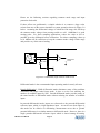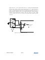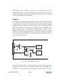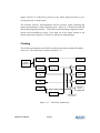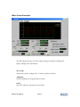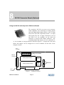
1
Acquitek CM Series
Multifunction Analog I/O Boards for PCI Bus
User Manual
July 2004
Information in this document is subject to change without notice.
© Copyright 2004, Acquitek, SAS. All rights reserved.
Acquitek is a trademark of Acquitek, SAS. Other trademarks and trade names may be used in
this document to refer to either the entities claiming the marks and names or their products.
Acquitek, disclaims any proprietary interest in trademarks and trade names other than its own.
Acquitek makes no warranty of any kind with regard to this material, including, but not limited to,
the implied warranties of merchantability and fitness for a particular purpose. Acquitek shall not
be liable for errors contained herein or for incidental or consequential damages in connection with
the furnishing, performance, or use of this manual.
Acquitek, SAS.
12 avenue des prés
Montigny le Bretonneux
78059 Saint-Quentin en Yvelines
France
Acquitek CM Series
Multifunction Analog I/O Boards for PCI Bus
TABLE OF CONTENTS
1 Introduction ..................................................................................................................5
Features:......................................................................................................................... 6
CM Series Product Line: ...................................................................................................7
2 Installation ....................................................................................................................8
CM Series Installation ....................................................................................................8
3 Hardware Overview ..................................................................................................10
Hardware Overview................................ ................................ ................................ ...... 10
Connectors .................................................................................................................. 12
Analog Inputs............................................................................................................... 14
Analog Outputs............................................................................................................ 22
Digital I/O ..................................................................................................................... 22
Counter/Timers ............................................................................................................ 23
Triggers........................................................................................................................ 24
Clocking....................................................................................................................... 25
Accessories ................................................................................................................. 27
4 Acquitek Control Center ........................................................................................30
Menu and Toolbar ........................................................................................................ 31
System Tree Pane ........................................................................................................ 32
Configuration Pane ................................ ................................ ................................ ...... 33
Info Tab ........................................................................................................................ 34
Configuration Tab ........................................................................................................ 35
Test Tab ....................................................................................................................... 36
5 Acquitek Bench........................................................................................................37
Menu and Toolbar ........................................................................................................ 38
DC Source .................................................................................................................... 40
Logic Analyzer ............................................................................................................. 41
Volt Meter ..................................................................................................................... 44
Oscilloscope ................................................................................................................ 46
Spectrum Analyzer....................................................................................................... 49
Strip Chart Recorder .................................................................................................... 51
Wave Form Generator .................................................................................................. 53
6 Third Party Drivers ..................................................................................................55
LabVIEW ................................ ................................ ................................ ...................... 55
MATLAB....................................................................................................................... 57
TestPoint................................ ................................ ................................ ...................... 59
ExcelDA – Microsoft Excel Add-In ................................................................................ 61
DASYLab ................................ ................................ ................................ ...................... 66
7 Technical Specifications .......................................................................................70
8 B-1350 Connector Board (Optional) ...................................................................74
Using the B-1350 with Acquitek CM-Series Boards ............................................................. 74
9 Cables & Connectors (Optional) ..........................................................................78
9 Cables & Connectors (Optional) ..........................................................................79
10 Glossary ...................................................................................................................82
11 Technical Support .................................................................................................87
1
Introduction
The Acquitek CM Series of multifunction analog I/O boards was designed to
provide high speed and 16 Bit precision at a low price to meet challenging PCbased instrumentation applications. All CM Series boards utilize an onboard
processor, large local memory buffers, and PCI bus mastering to provide glitchfree capture and output of analog waveforms with nearly unlimited lengths. This
performance is provided even under non-realtime PC operating systems when
running complex user applications, which are supported by a comprehensive
Software Development Kit and sample code.
With up to 32 inputs sampled at up to 1 MHz and flexible trig gering, the CM
Series is ideal for high-speed automation and control applications. The onboard
DSP coprocessor can offload critical real- time tasks, such as event-driven channel
sequence changes or sensor input linearization (through look up tables or
computation), to free the host program for higher- level algorithms and
applications. The outputs are waveform quality with both waveform playback
capability and function generation, or they can be slaved to the input channel
sequence. The board is PCI Plug-and-Play and autocalibrating, so there are no
jumpers or potentiometers to manually adjust.
CM-Series User Manual
Page 5
Features:
•
16/32 Single Ended Inputs (8/16 in Differential Mode)
•
Up to 1 MS/s Maximum Sampling Rate
•
16 Bit A/D Resolution
•
Up to 16 MB (8 MSample) Local Acquisitio n Memory
•
64K Channel-Gain List
•
Flexible Triggering Modes
•
Up to 2 Output Channels (Waveform Quality)
•
Up to 1 MS/s D/A Converter per Channel
•
16 Bit D/A Resolution
•
Up to 16 MB (8 MSample) Local Waveform Memory
•
1 Hz Sample Clock Resolution from onboard DDS
•
16/32 Digital I/O’s (synchronous with analog I/O)
•
Up to 3 Counter/Timers
•
PCI Bus-Mastering Transfers
•
Onboard 143 MHz, 32 Bit DSP for Real- Time Processing and Control
•
Windows 98/Me/2000/XP, Linux Compatibility
CM-Series User Manual
Page 6
CM Series Product Line:
CM Series - 250 kHz (1x, 2x, 4x, 8x Gain)
CM-2120
CM-2110
CM-2150
CM-2140
16 analog in, 16 digital I/O, 2 analog outputs, 250 kHz
16 analog in, 16 digital I/O, 0 analog outputs, 250 kHz
32 analog in, 32 digital I/O, 2 analog outputs, 250 kHz
32 analog in, 32 digital I/O, 0 analog outputs, 250 kHz
CM Series - 250 kHz (High Gain: 1x,10x,100x,1000x Gain)
CM-2121
CM-2111
CM-2151
CM-2141
16 analog in, 16 digital I/O, 2 analog outputs, 250 kHz
16 analog in, 16 digital I/O, 0 analog outputs, 250 kHz
32 analog in, 32 digital I/O, 2 analog outputs, 250 kHz
32 analog in, 32 digital I/O, 0 analog outputs, 250 kHz
CM Series - 1 MHz (1x, 2x, 4x, 8x Gain)
CM-2220
CM-2210
CM-2250
CM-2240
16 analog in, 16 digital I/O, 2 analog outputs, 1 MHz
16 analog in, 16 digital I/O, 0 analog outputs , 1 MHz
32 analog in, 32 digital I/O, 2 analog outputs, 1 MHz
32 analog in, 32 digital I/O, 0 analog outputs, 1 MHz
CM Series - 1 MHz (High Gain: 1x,10x,100x,1000x Gain)
CM-2221
CM-2211
CM-2251
CM-2241
CM-Series User Manual
16 analog in, 16 digital I/O, 2 analog outputs, 1 MHz
16 analog in, 16 digital I/O, 0 analog outputs, 1 MHz
32 analog in, 32 digital I/O, 2 analog outputs, 1 MHz
32 analog in, 32 digital I/O, 0 analog outputs, 1 MHz
Page 7
2
Installation
CM Series Installation
To install the CM Series hardware and software, complete the following steps:
Install the Acquitek Data Acquisition Hardware
•
•
•
•
•
•
•
•
Turn off your computer and disconnect the power cord.
Remove the computer cover.
Locate a free PCI expansion slot.
Carefully remove the card from its packaging.
Press the card into the PCI expansion slot.
Insure that the card is fully seated.
Reinstall the computer cover.
Reconnect the power cord.
Connect the Cables
•
Connect the IO cables to your external devices or breakout board.
Install the Windows Device Drivers
•
•
•
•
•
•
Turn on the computer.
When Microsoft Windows boots, it should discover the new device and launch
the New Hardware Wizard.
Insert the Acquitek Data Acquisition Setup CD into your CD-ROM drive.
Direct the New Hardware Wizard to search the CD-ROM drive for the device
drivers.
Windows may warn that the drivers are not authenticated. Proceed with
installation.
After the drivers are installed, remove the CD and reboot your computer.
CM-Series User Manual
Page 8
Install the Application Software and Third Party Drivers
•
•
•
•
Insert the Acquitek Data Acquisition Setup CD into your CD-ROM drive.
Run Setup.exe from the root directory of the CD
Follow the onscreen instructions to install the application and driver software. It
is recommended that you leave installation options unchanged to perform a full
installation of all software components.
After the installation completes, remove the CD and reboot your computer.
Configure the Data Acquisition Hardware
•
•
•
•
Run Acquitek Control Center from the Acquitek program group on the Windows
Start menu.
The new data acquisition device should appear as a node in the Local System |
Hardware | Acquitek | PCI/PXI branch of the System tree. Click on the node.
The serial number and logical device number will display in the Configuration
pane. The logical device number is the tag that all application software uses to
specify which hardware device will be used.
To change the assigned device number, click on the configuration tab and select a
new number using the device number edit control. Clic k the save button to make
the change permanent.
Test the Data Acquisition Hardware
•
•
•
If Acquitek Control Center is not still running, re-run the application from the
Acquitek program group on the Windows Start menu and select the System tree
node for the data acquisition device.
Select the Test tab in the Configuration pane.
The displayed test panels can be used to test all analog input channels and analog
output channels as well as the digital IO lines. Connecting an analog output to an
analog input, then turning on both panels can be used as a quick check to verify
basic operation.
Run Application Software
•
•
•
Installation and configuration of the Acquitek data acquisition hardware and
software is now complete.
You can run the included Acquitek Bench application software to use the device
in a wide range of test and measurement tasks.
Remember that all application software will refer to the data acquisition
hardware using the logical number assigned by Acquitek Control Center.
CM-Series User Manual
Page 9
3
Hardware Overview
Hardware Overview
The Acquitek CM Series of multifunction analog I/O boards was designed to
provide high speed and 16 bit precision at a low price to meet challenging PCbased instrumentation applications. All CM Series boards utilize an onboard
processor, large local memory buffers, and PCI bus mastering to provide glitchfree capture and output of analog waveforms with nearly unlimited lengths. This
performance is provided even under non-realtime PC operating systems when
running complex user applications, which are supported by a comprehensive
Software Development Kit and sample code. With up to 32 inputs sampled at up
to 1 MHz and flexible triggering, the CM Series is ideal for high-speed
automation and control applications. The onboard DSP coprocessor can offload
critical real-time tasks, such as event-driven channel sequence changes or sensor
input linearization (through look up tables or computation), to free the host
program for higher-level algorithms and applications. The outputs are waveform
quality with both waveform playback capability and function generation, or they
can be slaved to the input channel sequence. The board is PCI Plug-and-Play and
autocalibrating, so there are no jumpers or potentiometers to manually adjust.
The CM architecture is shown below in figure 3-1.
CM-Series User Manual
Page 10
Aux I/O
(Header)
Local Control Bus
(16)
Analog In
Gain &
Offset
Trim
16 SE/
8 DI
(16)
Control, Timing, and
Data Management FPGA
16 Bit, 1 MHz A/D
Converter
16 SE/
8 DI
(32)
+
Precision 2.5V Ref
VRef
_
Input Data
(3)
Analog Out 0
(3)
Ext Clk
Ext Trig
Sync
Int Clk
Output Data
SCSI 68 Connector
I/O
Drvr/
Rcvr
32 Digital I/O
(16)
Gain &
Offset
Trim
Local Control Bus
Calibration
EEPROM
(16/32)
8/16 MBytes
133 MHz
SDRAM
VLIW Processor
16 Bit, 1 MHz D/A
Converter
16 Bit, 1 MHz D/A
Converter
Addr/Data
PCI Bus Master Unit
Gain &
Offset
Trim
Command
Analog Out 1
32 Bit, 33 MHz PCI Bus
Figure 3-1 – CM Board Block Diagram
The mechanical layout of the CM Series board is depicted in Figure 3-2 below.
Depending upon the revision, the board may appear as in Figure 3-2a or 3-2b.
The functionality of the boards did not change, only the connector locations. All
members of the CM family share the same board footprint. Family members
without analog outputs will have unpopulated components in the analog output
section.
CM-Series User Manual
Page 11
Pin 1
Aux IO Header
Analog Input Section
FPGA
Analog Output Section
DSP/
PCI
Interface
SDRAM
68 Pin SCSI
Pin 1
Figure 3-2a – CM Board Layout
Secondary I/O
68 Pin VHDCI
Pin 1
Analog Input Section
FPGA
Analog Output Section
DSP/
PCI
Interface
SDRAM
Primary I/O
68 Pin VHDCI
Pin1
Figure 3-2b – CM Board Layout
Connectors
Every CM board has a primary 68 pin female connector on which 16 analog
inputs, 16 digital I/O’s, two analog outputs (if applicable) and a variety of timing
and reference signals are brought out. The pinout of this connector is shown in
CM-Series User Manual
Page 12
Figure 3-3a below. An Acquitek B-1150/1155 is recommended for use with this
connector. The B-1150/1155 is described below in the Accessories section.
In addition, on an Acquitek 32 input board (i.e CM-2250), analog inputs 16-31
and digital I/O 16-31 are brought out to a second connector, which may be an
auxiliary 40 pin header (shown in Figure 3-3b) or a secondary 68 pin female
connector (shown in Figure 3-3c). An Acquitek B-1050/1055 is recommended
for use with the 40 pin header. The B-1050/1055 is described below in the
Accessories section. The B-1150/1155 is recommended for use with the
secondary SCSI connector.
AIn0/0+ AInGnd AIn9/1- AIn2/2+ AInGnd AIn11/3- AInGndSense0-15AIn12/4- AIn5/5+ AInGnd AIn14/6- AIn7/7+ AInGnd AOutGnd AOutGnd DGnd PortA0 PortA5 DGnd PortA2 PortA7 PortA3 PortB1 PortB3 PortB5 A/D Trig I/O Cntr1 Clk Cntr1 Gate Cntr1 Out DGnd A/D SeqSt I/O Cntr0 Clk DGnd DGnd -
68
67
66
65
64
63
62
61
60
59
58
57
56
55
54
53
52
51
50
49
48
47
46
45
44
43
42
41
40
39
38
37
36
35
34 - AIn8/033 - Ain1/1+
32 - AInGnd
31 - AIn10/230 - AIn3/3+
29 - AInGnd
28 - AIn4/4+
27 - AInGnd
26 - AIn13/525- AIn6/6+
24 - AInGnd
23 - AIn15/722 - AOut0
21 - AOut1
20- Reserved
19 - PortA4
18 - DGnd
17 - PortA1
16- PortA6
15 - DGnd
14 - +5V Fused
13 - PortB0
12 - PortB2
11 - PortB4
10 - PortB6
9 - DGnd
8 - +5V Fused
7 - DGnd
6 - D/A Trig I/O
5 - D/A SeqSt I/O
4 - DGnd
3 - Cntr0 Gate
2 - Cntr0 Out
1- PortB7
DB-68
(PCI Finger Edge)
Figure 3-3a – Primary CM DB-68
Pinout
CM-Series User Manual
Page 13
Gnd - 40
Gnd - 38
Cntr2 Gate - 36
PortD7 - 34
PortD5 - 32
PortD3 - 30
PortD1 - 28
PortC7 - 26
PortC5 - 24
PortC3 - 22
PortC1 - 20
Gnd - 18
AIn31/15- - 16
AIn30/14- - 14
AIn29/13- - 12
AIn28/12- - 10
AIn27/11- - 8
AIn26/10- - 6
AIn25/9- - 4
AIn24/8- - 2
39 - Gnd
37 - Cntr2 Out
35 - Cntr2 Clk
33 - PortD6
31 - PortD4
29 - PortD2
27 - PortD0
25 - PortC6
23 - PortC4
21 - PortC2
19 - PortC0
17 - AInGndSense16-31
15 - AIn23/15+
13 - AIn22/14+
11 - AIn21/13+
9 - AIn20/12+
7 - AIn19/11+
5 - AIn18/10+
3 - AIn17/9+
1 - AIn16/8+
40 Pin Header
Figure 3-3b – CM Aux Header
Pinout
AIn16/8+ AInGnd AIn25/9- AIn18/10+ AInGnd AIn27/11- AInGndSense16-31 AIn28/12- AIn21/13+ AInGnd AIn30/14- AIn23/15+ AInGnd AOutGnd AOutGnd DGnd PortC0 PortC5 DGnd PortC2 PortC7 PortC3 PortD1 PortD3 PortD5 NC NC NC NC DGnd NC Cntr2 Clk DGnd DGnd -
68
67
66
65
64
63
62
61
60
59
58
57
56
55
54
53
52
51
50
49
48
47
46
45
44
43
42
41
40
39
38
37
36
35
34 - AIn24/833 - Ain17/9+
32 - AInGnd
31 - AIn26/1030 - AIn19/11+
29 - AInGnd
28 - AIn20/12+
27 - AInGnd
26 - AIn29/1325- AIn22/14+
24 - AInGnd
23 - AIn31/1522 - AOut0
21 - AOut1
20- NC
19 - PortC4
18 - DGnd
17 - PortC1
16- PortC6
15 - DGnd
14 - +5V Fused
13 - PortD0
12 - PortD2
11 - PortD4
10 - PortD6
9 - DGnd
8 - +5V Fused
7 - DGnd
6 - NC
5 - NC
4 - DGnd
3 - Cntr2 Gate
2 - Cntr2 Out
1- PortD7
Figure 3-3c – Secondary CM DB68 Pinout
Analog Inputs
The Acquitek CM board has up to 32 analog inputs which are multiplexed into a
programable gain instrumentation amplifier and then converted into digital data
by a 16 bit successive approximation A/D. The analog inputs are high impedance
to prevent undesired loading of the system to be measured. High impedance
inputs are prone to noise pickup. While crosstalk between channels of the CM
board is small, best performance can be obtained by grounding unused inputs or
capacitively coupling them to ground or to the reference in differential mode.
This will minimize any chance for crosstalk. Additionally, it is possible for noise
on an unused, unconnected input to saturate the instrumentation amplifier,
particularly in high gain applications. The recovery time of the instrumentation
amplifier from saturation is longer than normal switching time. Taking
CM-Series User Manual
Page 14
precautions not to leave unused inputs floating will minimize the chance that such
an input could be selected inadvertently leading to unexpected saturation and
issues with switching.
Signal Input Modes
Three input modes are available to suit a variety of applications. A knowledge of
the analog input signal modes and operation will help in achieving the maximum
performance in any application.
Single Ended – In single ended mode, the input voltage is measured with respect
to system ground at the computer. As shown in Figure 3-4, this can work well on
a floating source.
+
++
-
+
Vsignal
-
+
Measured V
- at A/D
Figure 3-4 – Single Ended, Floating Source
However, as shown in Figure 3-5, in the situation where the source is referenced,
problems may arise. It is common for the source being measured to have a
different reference potential than the measurement computer, for example if they
are powered from different circuits of the electrical distribution system. In this
case, the resulting voltage measured by the A/D converter is Vsignal + Vcm,
where Vcm is the potential difference between the source ground and
measurement computer ground. This can easily be on the order of volts in a
typical commercial setting, and fluctuate as loads are connected or removed from
the electrical distribution system.
CM-Series User Manual
Page 15
++
V signal
-
++
-
+
-
+
Vcm
-
Measured V
at A/D
Wire
Resistance
Figure 3-5 – Single Ended, Referenced Source
Finally, as shown in Figure 3-6, even the simple floating source scenario shown in
Figure 3-4 can result in measurement errors due to noise pickup. This is because
the signal line terminates in a high impedance PGIA input, while the reference
line terminates in low impedance ground. The noise pickup will be far more
severe on the high impedance signal line, resulting in the measurement of Vsignal
+ Vnoisepickup at the A/D converter. The noise pickup will be most severe in
long cable runs and with high impedance sources.
+
V noise
++
V signal
-
++
-
+
Measured
V
at A/D
Figure 3-6 – Single Ended, Floating Source + Noise
CM-Series User Manual
Page 16
For the given considerations, it is recommended that single ended mode only be
used under the following conditions:
•
cable runs of less than 3 meters, and
•
signal levels of 1V or greater, and
•
common power ground between input source and measurement
computer.
Differential – Differential mode eliminates many of the problems associated with
single ended input mode. As shown in Figure 3-7, a referenced source with a
different reference potential than the measurement computer results in no
measurement error when using differential mode.
++
V signal
-
++
-
+
Measured V
- at A/D
+
V cm
-
Figure 3-7 – Differential, Referenced Source
Also with differential mode, measurement error due to noise pickup is also
reduced as compared to the single ended case. This is because both lines in the
differential pair are terminated by a high impedance PGIA input. As long as both
lines pass through essentially the same electromagnetic fields, which is the case
when using twisted pair wires or wires in close proximity to each other, the noise
induced on each line will be the same. The PGIA will reject the noise which is
common to both lines of the differential pair.
When using differential mode with floating sources, care must be taken to keep
the floating source within the common mode range of the CM board and outside
the range which will trigger the input protection circuitry on the input multiplexer.
CM-Series User Manual
Page 17
Please see the following sections regarding common mode range and input
protection for details.
If these effects are problematic, a simple solution is to connect a large value
resistor from one of the source terminals to system ground as shown in Figure 3-8
below. Assuming the differential voltage is within the CM range, this will keep
the common mode voltage from causing trouble as well. 100KOhm is a good
starting point. For faster sampling applications, reduce the value as low as
possible given the differential source constraints. For slower sampling, values up
to 10 MOhm will be sufficient to keep the common mode voltage within range
and provide very little source loading.
++
Vsignal
-
++
-
+
-
R=100K
Measured V
at A/D
Figure 3-8 – Differential, large common mode source
Differential mode is the recommended input operating mode in nearly all cases.
Pseudo-Differential – While differential mode eliminates many of the problems
associated with single ended input mode, it does so at the cost reducing the
number of available inputs by half. Pseudo-differential mode provides many of
the same benefits of differential mode without reducing the number of available
inputs.
In pseuedo-differenetial mode, inputs are referenced to the pseuedo-differenetial
reference input, which is a high impedance input. As can be seen from Figure 9,
this mode can be effective in eliminating measurement errors due to ground
potential differences in a similar manner to differential mode. However, there is a
single pseuedo-differenetial reference input which is shared among all analog
CM-Series User Manual
Page 18
inputs from 0-15. On 32 input boards, there is a second pseuedo-differenetial
reference input which is shared among analog inputs 16-31. Again referring to
Figure 3-9, pseuedo-differenetial mode will eliminate measurement errors due to
ground potential difference only if all pseuedo-differenetial inputs sharing a
common pseuedo-differenetial reference input also share the same voltage
reference (which need not be the same as the measurement computer ground
reference).
+
V signal
-
++
-
++
V signal
-
-
+
V cm
-
Figure 3-9 – Pseudo-Differential inputs
CM-Series User Manual
+
Page 19
Measured V
at A/D
Common Mode Range
As shown in Figure 3-9 above, the instrumentation amplifier will not measure any
signal between its inp uts and ground, and only measure the difference between
the voltages at its inputs. Both input signals must be in the range AinGnd – 10V
to AinGnd + 10V in order for the instrumentation amplifier to function correctly.
Input Protection
As shown in the CM block diagram (Fig 3-1), the input multiplexer is the first
component through which the analog inputs pass following the connector. The
input multiplexer is fault protected to protect it and the downstream components
from damage if the input is inadvertently connected to a source voltage outside
the analog input range. The overvoltage protection range is listed in the board
specifications section. When the overvoltage protection is operating, the mux
goes into a high impedance state and negligible current will flow into or from the
board.
It is possible that a floating source will have enough static charge that its common
mode voltage is in the range where the overvoltage protection is operable. In this
event, since the mux is high impedance, no current will flow from the floating
source to dissipate its common mode potential. It is therefore advisable to
connect a high value resistor to reference a floating source to the CM board
ground (10 MOhm is sufficient to drain static charge, but 10 kOhm may be
preferable in a fast switching application).
Input Bias Current
The PGIA on the CM Series boards, like all instrumentation amplifiers, requires a
return path for the bias currents at its inputs. In the case of the CM Series, the
bias currents are extremely small, typically less than 10 pA. On the CM Series
boards, there are onboard bias resistors of 10 MOhm on both the positive and
negative PGIA inputs. These provide a path for the PGIA input bias current and
introduce less than 100uV of measurement er ror. On a typical low impedance,
referenced source, most of the bias current will flow through the source resistance
and the measurement error will be much smaller. Having the bias resistors on
board simplifies connection to a floating source, subject to the limitations
discussed above in the Input Protection section. Without these onboard resistors,
one or both terminals of a floating source would always require a resistive
connection to ground to provide input bias current.
CM-Series User Manual
Page 20
Multi-Channel Scanning
The CM series of multifunction boards can scan multiple inputs at the maximum
sampling rate of the board. However, settling times of the analog input system
must be accounted for in order to achieve accurate measurement results. Settling
time is the amount of time required for a system to respond to a transient input
event, such as an input switch in a multiplexed data system. If all of the inputs to
be sampled are of similar magnitude and on the same input range, settling time
may not be a factor. However, if different gains are used between input channels,
it will be very important to consider how settling time may affect measurement
accuracy. Settling times for the CM input and outputs are provided in the
specifications section.
Settling time during multi-channel scanning is also adversely affected by a
multiplexer property called charge injection. The analog input multiplexer injects
a small amount of charge (given in the specifications section) into the selected
input upon switching. This introduces a voltage error on the input equal to the
charge injected divided by the input capacitance. The voltage error will decay
according to the RC time constant of the input resistance and capacitance. High
impedance inputs will cause the voltage error to take longer to decay, and thus the
settling time could increase.
Note that if an input signal saturates the PGIA, there is a significantly longer
overload recovery time than the normal PGIA settling time when switching inputs
in a non-saturated case. Therefore it is strongly advised to select input ranges
which will not cause the PGIA to become saturated. For the same reason, it is
also suggested that unused inputs be grounded (in single ended mode) or tied to
the reference signal (differential mode) to prevent noise pickup from saturating
the PGIA if an unused input is inadvertently selected in the multichannel scan.
As discussed above, there are several potential pitfalls with multi- channel
scanning. The user should consider alternatives to simple multi-channel scanning
if in doubt about any of the above settling time limitations to avoid any channel to
channel dependencies. One such alternative is to acquire multiple points
consecutively from each channel before switching to the next channel. These
points can be averaged to reduce the effects of system noise or noise pickup on
cables. If multi-channels scanning is used, always use low impedance input
sources.
CM-Series User Manual
Page 21
Analog Outputs
Only applicable to boards equipped with analog outputs (CM-2120/2121, CM2150/2151, CM-2220/2221, CM-2250/2251).
Many members of the CM Series are equipped with two analog outputs. These
outputs have software selectable output ranges of 0 to 10V and –10 to +10V. In
the unipolar mode, the data format is straight binary. In bipolar mode, the data
format is two’s complement.
The analog outputs can operate in quasi-static or clocked mode. The output
circuitry has been designed with both high accuracy and fast settling time to
permit output of high quality waveforms. The onboard DSP, deep onboard FIFO,
and PCI bus mastering ensure reliable output of waveforms or other sequences at
the full sample rate.
The outputs should not drive loads less than 2 KOhms. Output accuracy may be
degraded with a lower resistance load. The ouputs are short circuit current
limited, but care should be taken to avoid long duration output shorts as the
thermal strain may eventually damage the output driver.
Digital I/O
Each CM Series board has several digital I/O pins. The number of digital I/O’s is
equal to the number of analog inputs on the board. The digital I/O’s are grouped
into 8 bit ports. Each port can be configured as an input or output port. All 8
lines in each port are configured in the same direction. Upon reset, the port is
configured as an input.
The digital I/O architecture uses a 74ACT gate as the driver and receiver, along
with a 10 KOhm pull up resistor on each I/O. The 74ACT receiver has TTL
compatible input logic thresholds and and the driver can source or sink 24 mA
output cur rent.
The digital I/O’s are capable of quasi-static operation or clocked mode. In
clocked mode, each digital I/O is read on a clock which can be synchronous with
the analog input clock. Thus, every digital I/O can be read at the maximum
CM-Series User Manual
Page 22
sample rate of the board. Output is similar. All digital I/O’s can be updated on a
clock which can be synchronous with the analog output clock. In clocked mode,
the digital I/O’s share FIFO space with the analog inputs and outputs, but this has
no detrimental effect on the analog signals since the FIFOs on the CM Series of
boards are so large.
Counter/Timers
The CM series of boards are equipped with two or three identical counter/timer
circuits. Each counter/timer circuit is fully available to the user; they are not used
to provide timing clocks to either the analog inputs or analog outputs. The
counter/timers emulate 82C54 operating modes as described below:
§ Mode 1: Retriggerable One Shot
Out is high. Rising edge on gate triggers out to go low and down counting
to start. Out stays low until count expires, at which point out goes high.
§ Mode 2: Rate Generator
Out is high. Gate high enables down counting. When count expires, out
goes low for one clock cycle, then high again. Count is reloaded and
down counting continues. This results in a sequence of negative pulses of
width 1/clockFreq and period countReg/clockFreq being generated while
gate is active.
§ Mode 3: Square Wave Generator
Out is high. Gate high enables down counting. When count reaches
count/2, out goes low. When count expires, out goes high. Count is
reloaded and down counting continues. This results in a square wave of
approximately 50% duty cycle and period countReg/clockFreq being
generated while gate is active.
§ Mode 5: Retriggerable Strobe
Out is high. Rising edge on gate triggers down counting to start. Out
stays high until count expires, at which point out goes low for one clock,
then high again.
Note the countReg on the CM-22xx Series timers is 24 bits as compared to the 16
bit count registers on the 82C54. This provides for more versatility at high clock
rates.
The clock source is software selectable from either the on-board sample clock or
the external counter clock input pin. The gate source is also software selectable
between software controlled gating or gating from an external pin. The
CM-Series User Manual
Page 23
counter/timer output is available on a pin and can also trigger an interrupt in the
onboard DSP. There is a separate external clock, gate, and output pin for each
counter. The Acquitek Data Acquisition SDK has documentation on the functions
used for programming the counter/timers.
Triggers
The CM Series have many triggering options. Digital trigger inputs and outputs
are available on the main connector to signal the start of a conversion, the start of
an input sequence, the start of an output sequence, or an output update. Analog
triggering is typically implemented in the board hardware by comparing the past
and present A/D converter output values with register values corresponding to the
trigger voltage and slope. Additionally, an analog trigger is available. It lies
between the PGIA and the A/D converter as shown in Figure 3-10, and thus
operates on a scaled, multiplexed input signal. The analog comparator triggering
can be useful in detecting glitches on a signal which is being sampled at a low rate
relative to the glitch duration.
+
A/D
converter
++
PGIA
++ Analog Trigger
DSP
++
Aout1
Figure 3-10 – Analog Trigger Architecture
As can be seen from Figure 3-10, analog output 1 is used to set the trigger level,
and thus can not be used as a general purpose output while analog triggering is
operational. Also, on CM Series boards without analog outputs, the analog
CM-Series User Manual
Page 24
trigger reference is connected to ground, so the analog trigger becomes a zerocrossing detector on such boards.
The Acquitek software API implements all the necessary signal switching and
register programming to make triggering work. However, it should be noted that
both analog triggering methods – A/D value based and analog comparator based –
operate on the multiplexed signal. If an input set as the trigger channel is not
present in the input sequence, it will never generate an analog trigger.
Clocking
The clocking mechanism on the CM Series boards provides maximum flexibility
to the user. The architecture is shown in Figure 3-11.
÷N
Analog
Outputs
DDS
÷M
(1 Hz Res)
(M>40)
Analog
Inputs
DDS
66 MHz
Crystal
Oscillator
(1 Hz Res)
C/T 0 Ext
Clk
Counter/
Timer 0
C/T 1 Ext
Clk
Counter/
Timer 1
C/T 2 Ext
Clk
Counter/
Timer 2
÷ 64
4
Independent Clk
mux control
Figure 3-11 – CM Clock Architecture
CM-Series User Manual
Page 25
As shown in Figure 3-11, the analog inputs and counter/timers can be driven from
an external clock. The external clock source must be a TTL-compatible square
wave.
The analog input section shares its external clock source with
Counter/Timer 2 on CM-22xx boards. On CM-21xx boards with only two
counter/timers, the analog input external clock is not shared. It must still be
applied to the connector pin labeled Cntr2 Clk. In external clock mode, the
analog input sample rate is equal to the external clock frequency divided by 64.
This factor is required for the pipeline delay of the A/D converter and the trim
DACs which calibrate the analog input on a sample by sample basis according to
the range setting in the channel- gain list. In internal clock mode, the
counter/timers run off a clock that is an integer multiple M of the analog input
sample rate. Again, M is large (between 40 and 64k) to facilitate the analog input
pipeline. The Acquitek Data Acquisition SDK has documentation on the
functions used for programming the clock sources and frequencies.
CM-Series User Manual
Page 26
Accessories
There are several accessories available to simplify connecting signals to and from
the CM Series boards. All CM Series boards use a 68 pin female connector as the
primary I/O connector. The analog inputs 0-15, the digital I/O Ports A and B, the
analog outputs (if applicable) and timing and reference signals are available on
this connector. The Acquitek B-1150/1155 is a breakout board for this connector.
The layout of the B-1150/1155 is shown in Figure 3-12 below.
The B-1150/1155 is available in either a stand alone board format (B-1155) or in
a rackmountable box format (B-1150). In the standalone board format,
connectors J9, J10, and J11 will not be populated. In the rackmountable box
format, connectors J2, J3, J5, J6, and J8 will not be populated since they are
duplicated by J9, J10, and J11. J4 and J7 will be populated since there is not
enough space to bring the signals on these connectors out to the box edge.
With a 32 input CM Series board, analog inputs 16-31 and digital I/O Ports C and
D are brought out to either a 40 pin header or a secondary VHDCI-68 female
connector on the CM board. The Acquitek B-1050/1055 is a breakout board for
the 40 pin header. The layout of the B-1050/1055 is shown in Figure 3-13 below.
The B-1050/1055 is available in either a stand alone board format (B-1055) or in
a rackmountable box format (B-1050). In the standalone board format,
connectors J3, J5, and J8 will not be populated. In the rackmountable box format,
connectors J1, J2, J4, J6, and J7 will not be populated since they are duplicated by
J3, J5, and J8. J9 will be populated since there is not enough space to bring the
signals on this connector out to the box edge.
If the 32 input CM Series board uses a secondary VHDCI-68 connector, a second
B-1150/1155 should be used. The secondary I/O connector pinout matches the
primary I/O connector, so usage is easy:
§ Secondary I/O PortC pins => B-1150 PortA pins
§ Secondary I/O PortD pins => B-1150 PortB pins
§ Secondary I/O Cntr2 pins => B-1150 Cntr0 pins
§ Secondary I/O Ain pins => B-1150 Ain+16 (SE) or Ain+8 (Diff) pins
CM-Series User Manual
Page 27
Figure 3-12 – B-1150/1155 Layout
CM-Series User Manual
Page 28
Figure 3-13 – B-1050/1055 Layout
CM-Series User Manual
Page 29
4
Acquitek Control Center
Acquitek Control Center (ECC) provides a central location for the configuration
and test of data acquisition products from Acquitek . ECC is used to assign logical
device numbers to Acquitek hardware devices so that those devices can be
accessed from other software applications. ECC can also be used to specify
default configuration parameters for Acquitek hardware devices and to verify
correct installation and operation of those devices.
CM-Series User Manual
Page 30
Menu and Toolbar
File / Load Profile
Loads a previously saved set of configuration data, making those settings active.
File / Save Profile
Save the current configuration settings for all Acquitek devices to a named file.
File / Exit
Exit Acquitek Control Center
Edit / Preferences
Set general application preferences including whether to scan hardware and
software each time Acquitek Control Center is started.
View / Refresh
Scan the system for installed hardware and software
Help / Contents
View help for Acquitek Control Center
Help / Acquitek Web Site
Open the Acquitek home page in a default browser window
Help / About
Display version and copyright information for Acquitek Control Center
CM-Series User Manual
Page 31
System Tree Pane
The System Tree Pane displays a graphical representation of the hardware and
software discovered during the last system scan. This information can be updated
by selecting View / Refresh from the main menu.
There are separate branches on the tree representing Acquitek hardware devices,
system and third party hardware devices, Acquitek software components, OS
software components, and third party software components. The leaves on the
branches can be selected to display additional information in the Configuration
Pane.
CM-Series User Manual
Page 32
Configuration Pane
The Configuration Pane displays one or more tabbed pages with additional
information about the hardware device or software module currently selected in
the System Tree.
CM-Series User Manual
Page 33
Info Tab
The information displayed on the Info Tab varies according to the device or
module selected in the System Tree. Selected Acquitek hardware devices display
their serial number and the configured device number. Other hardware devices
display PCI configuration data. Software modules display version resource
information if available along with file date and size.
CM-Series User Manual
Page 34
Configuration Tab
The Configuration Tab is only available when an Acquitek hardware device is
selected in the System Tree Pane. This page is used to set the logical device
number for Acquitek devices to be used by other software applications.
CM-Series User Manual
Page 35
Test Tab
The Test Tab is only available when an Acquitek hardware device is selected in
the System Tree Pane. This page is used to test functionality of the selected
device. Select a device channel for analog IO, or configure direction for digital
IO, then activate the panel by clicking its 'On' button. Correct installation and
operation can be verified for all analog and digital channels.
CM-Series User Manual
Page 36
5
Acquitek Bench
Acquitek Bench is a collection of tools that enables a PC equipped with an
Acquitek data acquisition device to function as a DC voltage source, a logic
analyzer, a digital multimeter, an oscilloscope, a spectrum analyzer, a strip chart
recorder, and an arbitrary wave form generator
CM-Series User Manual
Page 37
Menu and Toolbar
The menu and toolbar are used to open and close the various instruments
windows and arrange the display of those windows.
File
Exit
Close Acquitek Bench
Edit
Preferences
Set application specific preferences
View
DC Source
Open or close the DC Source window
Logic Analyzer
Open or close the Logic Analyzer window
Meter
Open or close the Meter window
Oscilloscope
Open or close the Oscilloscope window
Spectrum Analyzer
Open or close the Spectrum Analyzer window
CM-Series User Manual
Page 38
Strip Chart
Open or close the Strip Chart window
Waveform Generator
Open or close the Waveform Generator window
Window
Cascade
Cascade all open child windows
Tile
Tile all open child windows
Minimize All
Minimize all open child windows
Close
Close the currently selected child window
Help
Contents
Display help contents
Acquitek Web Site
Launch the default browser and direct to www.Acquitek.com
About
Display version and copyright information
CM-Series User Manual
Page 39
DC Source
The DC Source is used to output a constant voltage on an analo g output channel.
Analog Out Channel
Zero based analog output channel number.
Device Number
Data acquisition device number as configured in Acquitek Control Center. You
must assign a device number to the acquisition board before it can be used in
Acquitek Bench or other application software.
CM-Series User Manual
Page 40
Logic Analyzer
The Logic Analyzer is used to capture and inspect logic level (0V - +5V) signals
using the digital IO lines.
SEC/DIV
Specify the number of seconds per division on the Horizontal Axis Displa y
Position (Time Base)
Specify the vertical offset of the entire channel in percent of the Display.
Pre-Capture
Specify how much data to capture before the beginning of the display. The value
is specified in divisions of the horizontal axis.
CM-Series User Manual
Page 41
Post-Capture
Specify how much data to capture after the end of the display. The value is
specified in divisions of the horizontal axis.
Level
Specify the level where the trigger mechanism will trigger a new frame to be
displayed.
Source
Specify the channel index used as the data source by the Trigger.
Slope
Specify whether a positive or negative slope is used when triggering.
Auto
Specify whether the Trigger is Automatic or Manual. If this value is FALSE, then
you must manually evaluate the Trigger by pressing the trigger button in the
Trigger section of the Scope Panel.
Volts/DIV
Specify the number of volts per division on the vertical axis display.
Position (Channel)
Specify the vertical offset of the entire channel in Percent of the Display.
Coupling
Specify the signal coupling of this channel.
Visible
Specify whether the channel trace line is visible.
Digital In Lines
Digital inputs which will be sampled and displayed. Only the first 8 DIOs can
currently be used.
Samples / Second
Input sampling rate.
CM-Series User Manual
Page 42
Device Number
Data acquisition device number as configured in Acquitek Control Center. You
must assign a device number to the acquisition board before it can be used in
Acquitek Bench or other application software.
Note: Additional configuration options can be accessed by right clicking on the
instrument.
CM-Series User Manual
Page 43
Volt Meter
The Volt Meter is used to measure voltages on analog input channels.
AC
Enable RMS AC signal measurement
Range
Voltage range of signal under test. Selecting 'Auto' will cause the volt meter to
automatically determine the smallest range which encompasses the measured
voltage, thereby yielding the highest precision.
Mode
Analog input type – differential (2 wire), single ended (1 wire), or non-referenced
single ended (1 wire)
Coupling
Analog input coupling and impedance
Analog In Channel
Zero based analog input channel number
CM-Series User Manual
Page 44
Device Number
Data acquisition device number as configured in Acquitek Control Center. You
must assign a device number to the acquisition board before it can be used in
Acquitek Bench or other application software.
CM-Series User Manual
Page 45
Oscilloscope
The Oscilloscope is used to provide a two-dimensional visual display of an analog
signal. Most commonly it is used to show signal amplitude versus time,
displaying the waveform of the signal being monitored.
SEC/DIV
Specify the number of seconds per division on the Horizontal Axis Display
Position (Time Base)
Specify the vertical offset of the entire channel in percent of the Display.
CM-Series User Manual
Page 46
Pre-Capture
Specify how much data to capture before the beginning of the display. The value
is specified in divisions of the horizontal axis.
Post-Capture
Specify how much data to capture after the end of the display. The value is
specified in divisions of the horizontal axis.
Level
Specify the level where the trigger mechanism will trigger a new frame to be
displayed.
Source
Specify the channel index used as the data source by the Trigger.
Slope
Specify whether a positive or negative slope is used when triggering.
Auto
Specify whether the Trigger is Automatic or Manual. If this value is FALSE, then
you must manually evaluate the Trigger by pressing the trigger button in the
Trigger section of the Scope Panel.
Volts/DIV
Specify the number of volts per division on the vertical axis display.
Position (Channel)
Specify the vertical offset of the entire channel in Percent of the Display.
Coupling
Specify the signal coupling of this channel.
Visible
Specify whether the channel trace line is visible.
CM-Series User Manual
Page 47
Mode
Analog input type – differential (2 wire), single ended (1 wire), or non-referenced
single ended (1 wire)
Coupling
Analog input coupling and impedance
Probe
Specifies a 1x, 10x, or 100x probe for scaling of display values.
Analog In Channel
Zero based analog input channel number
Device Number
Data acquisition device number as configured in Acquitek Control Center. You
must assign a device number to the acquisition board before it can be used in
Acquitek Bench or other application software.
Note: Additional configuration options can be accessed by right clicking on the
instrument.
CM-Series User Manual
Page 48
Spectrum Analyzer
The Spectrum Analyzer is used to measure the frequency spectrum of a signal on
an analog input channel.
Range
Voltage range of signal under test
Mode
Analog input type – differential (2 wire), single ended (1 wire), or non-referenced
single ended (1 wire)
Coupling
Analog input coupling and impedance
CM-Series User Manual
Page 49
Analog In Channel
Zero based analog input channel number
Samples / Second
Input sampling rate.
Device Number
Data acquisition device number as configured in Acquitek Control Center. You
must assign a device number to the acquisition board before it can be used in
Acquitek Bench or other application software.
CM-Series User Manual
Page 50
Strip Chart Recorder
The Strip Chart Recorder is used to capture and save voltage levels from the
analog input channels.
Range
Voltage range of signal under test
Mode
Analog input type – differential (2 wire), single ended (1 wire), or non-referenced
single ended (1 wire)
Coupling
Analog input coupling and impedance
CM-Series User Manual
Page 51
Probe
Specifies a 1x, 10x or 100x probe for scaling of display values.
Record
Activate logging of data to disk
File
Name of data log text file. Each line of the file contains a time offset value
followed by a tab, then the sample value and a carriage return
Analog In Channel
Zero based analog input channel number
Samples / Second
Input sampling rate.
Device Number
Data acquisition device number as configured in Acquitek Control Center. You
must assign a device number to the acquisition board before it can be used in
Acquitek Bench or other application software.
Note: Additional configuration options can be accessed by right clicking on the
instrument.
CM-Series User Manual
Page 52
Wave Form Generator
The Waveform Generator is used to output analog waveforms including sine,
square, triangle, DC, and arbitrary.
Wave Type
Selects sine, square, triangle, DC, or arbitrary (File) waveform
Amplitude
Sets the amplitude of the generated waveform
Offset
Sets a DC offset for the generated waveform
CM-Series User Manual
Page 53
WF File
When File wavetype is chosen, selects the file containing waveform data. Each
line of the file should contain a time offset value followed by a tab, then the
sample value and a carriage return.
Analog Out Channel
Zero based analog output channel number.
Frequency
Output cycles per second. Waveform files are assumed to be 1024 points per
cycle.
Range
Waveform amplitude min and max values.
Device Number
Data acquisition device number as configured in Acquitek Control Center. You
must assign a device number to the acquisition board before it can be used in
Acquitek Bench or other application software.
CM-Series User Manual
Page 54
6
Third Party Drivers
LabVIEW
The Acquitek Data Acquisition LabVIEW VIs provide a LabVIEW interface for
all calls available through the Acquitek Data Acquisition API. The names and
parameters are identical to those exported by XDADAQ.DLL.
CM-Series User Manual
Page 55
If the installation application was able to locate a LabVIEW installation on your
computer, the Acquitek VIs have been installed into the LabVIEW directory and
can be accessed from the LabVIEW function palette by choosing the Acquitek
Data Acquisition palette view. If a LabVIEW installation was not detected,
manual installation can be completed by copying the XDADaqLV and Menus
directories from the [installdir]\ThirdParty\LabVIEW directory into the main
LabVIEW installation directory (the directory containing LabVIEW.exe).
A number of sample VIs are included and can be found in the
[installdir]\ThirdParty\LabVIEW \Samples directory. These samples demonstrate
wiring of the API level VIs and can also be used as higher level building blocks
within new LabVIEW applications. The first time you attempt to open one of the
samples from the [installdir]\ThirdParty\LabVIEW\Samples subdirectory,
LabVIEW will not be able to find the XDADaqLV VIs used by the sample. You
can either browse to the correct [LabVIEW_Install] \XDADaqLV\* directory
using the 'find vi' dialog displayed by LabVIEW while loading the sample, or you
can permanently fix the problem for all samples by opening the LabVIEW 'Tools
/ Options' menu, selecting 'Paths' and 'VI Search Path' then entering
'[LabVIEW_Install]\XDADaqLV\*' and clicking 'Insert Before'. Note
'[LabVIEW_Install]' should be replaced by the actual name of the directory where
LabVIEW is installed on your system. Also note that the '\*' after XDADaqLV is
needed so that LabVIEW will search the subdirectories under XDADaqLV.
CM-Series User Manual
Page 56
MATLAB
Acquitek currently provides access to its data acquisition API in MATLAB via
MEX-files. These functions are contained in .dll files in the
\Acquitek\ThirdPary\MATLABMEX directory. Their help text documentation is
contained in .m files with filenames that correspond to the .dll files. To see this
documentation, type “help XXX" at the MATLAB prompt, where "XXX" is the
part of the filename before the .dll extension, such as "XDA_Ain_Volts." The
functions can be called just as any M- function is called. For example, to read a
sequence of 5000 input voltages between -5V and 5V from analog input channels
0 and 1 of device 1 at 10000 Hz, type the following at the MATLAB prompt:
[ch0 ch1] = XDA_Ain_Volts(1, [0 1], [5.0 5.0], 10000, 5000)
CM-Series User Manual
Page 57
The \Acquitek\ThirdPary\MATLABMEX directory currently contains MEX- files
for analog input and output, digital input and output, and counter/timer functions.
The analog input functions can be found in the following files:
XDA_Ain_Coupling.dll
XDA_Ain_Raw.dll
XDA_Ain_Volts.dll
Analog output functions can be found in the following files:
XDA_Aout_Func.dll
XDA_Aout_Raw.dll
XDA_Aout_Volts.dll
Digital input and output functions can be found in the following files:
XDA_Din_Read.dll
XDA_Dout_Write.dll
Counter/timer functions can be found in the following files:
XDA_CT_Config.dll
XDA_CT_Gate.dll
XDA_CT_Read.dll
Example M- functions that use these MEX-files can be found in the
\Acquitek\ThirdPary\MATLABMEX \Samples directory.
CM-Series User Manual
Page 58
TestPoint
Capital Equipment Corporation’s TestPoint is software for designing test,
measurement, and data acquisition applications. The Acquitek TestPoint driver
enables the use of all Acquitek hardware with TestPoint to simplify data
acquisition.
CM-Series User Manual
Page 59
Installation
•
•
•
Copy the file TPAcquitek.dll from
[AcquitekInstallDirectory]\ThirdParty\TestPoint to the directory where
TestPoint is installed.
Edit the TestPoint.ini file found in the TestPoint directory. Replace the entire
[AD0] section with this text:
[AD0]
manufacturer=AUTO
MODE=Bipolar
TYPE=Pseudo
COUPLING=DC
DACOUPLING=DC
Edit the TPAD.ini file found in the TestPoint directory. Find the
[ADDRIVERS32] section and add this line:
ACQUITEK WDM=TPACQUITEK.DLL
The Acquitek data acquisition board assigned logical device number one using
Acquitek Control Center can now be accessed in TestPoint as AD device zero. To
use multiple boards, or change the logical device t hat will be used, copy the board
configuration information added for [AD0] into another section ([ADn]). The
Acquitek device number will always be one greater than the TestPoint AD number.
Notes
You must run Acquitek Control Center to assign logical device numbers to all
Acquitek devices and verify basic functionality before using the devices with
TestPoint.
The TestPoint driver will be copied to the
[AcquitekInstallDirectory]\ThirdParty\TestPoint directory by Acquitek Setup.
You must complete the installation as documented above.
A sample TestPoint application called AD_DA.tst is copied to
[AcquitekInstallDirectory]\ThirdParty\TestPoint\samples by Setup. This
application can be used to verify basic functionality.
CM-Series User Manual
Page 60
ExcelDA – Microsoft Excel Add-In
ExcelDA is a Microsoft Excel Add-In that enables data acquisition from within
Excel using any Acquitek hardware device. It is included with all Acquitek
products and installed into the ThirdParty directory when Acquitek Data
Acquisition Setup is run.
Installation
To Install ExcelDA follow these steps:
•
•
•
•
•
•
•
•
Start Microsoft Excel
Choose 'Add-Ins...' from the Excel 'Tools' menu
Click the 'Browse...' button on the Add-Ins dialog
Navigate to [AcquitekInstallDirectory] \ThirdParty\ ExcelDA
Double click ExcelDA.xla
Click the 'OK' button on the Add-Ins dialog
Choose 'ToolBars' from the Excel 'View' menu
Select 'Acquitek Data Acquisition' from the ToolBars list
Once you have completed these steps, the Acquitek Data Acquisition toolbar will
be available for use with any workbook within Excel. You can drag and dock the
toolbar to a convenient spot on the Excel toolbar, or let it float within the work
area as you prefer.
CM-Series User Manual
Page 61
General Configuration
Display the General Configuration tab on the configuration dialog by clicking
'Configure' on the Acquitek Data Acquisition toolbar, then choosing the 'General'
tab.
Device Number
Logical device number of the Acquitek hardware device that will be used for acquisition.
This number must be assigned in Acquitek Control Center.
Target Workbook
The workbook to which data will be acquired. You must provide the entire name
including the .xls extension if one is present.
Target Worksheet
The worksheet to which data will be acquired. This sheet must already be present in the
specified workbook.
Target Column
Starting Column for data acquisition. Data for a single channel will be captured to the
specified column. Data for multiple channels will be captured to consecutive columns.
Target Row
Starting row for data acquisition. Samples for each channel will be captured in
consecutive rows starting with the specified row.
CM-Series User Manual
Page 62
Analog In Configuration
Display the Analog In Configuration tab on the configuration dialog by clicking
'Configure' on the Acquitek Data Acquisition toolbar, then choosing the 'Analog
In' tab.
Channel Count
The number of channels from which data will be acquired.
Sample Count
The number of samples to acquire from each channel. Note that Excel limits this value to
about 65000.
Sample Rate
The sampling clock frequency to be used for the acquisition.
Scan Rate
The time between channel sample sets when using hardware that does not support
simultaneous sampling. Set this value to 0 when acquiring one channel or when you wish
to use the frequency specified by 'Sample Rate'.
Range
The maximum voltage of the input signal. Valid values for this parameter depend on the
particular hardware device being used. Please see the hardware reference manual for a
list of valid values.
CM-Series User Manual
Page 63
Polarity
Input signal polarity - Bipolar or Unipolar.
Coupling
Input signal coupling - AC, DC, or DC Terminated.
Mode
Input signal mode - Differential, Single Ended, or Pseudo Differential.
Trigger Channel
Analog channel used to trigger acquisition.
Trigger Level
Voltage level at which data acquisition will trigger.
Trigger Type
Trigger mode - Falling, Rising, External, or None. To begin acquisition as soon as the
'Acquire' toolbar button is clicked, set this value to none.
Trigger Noise Reject
Enable Trigger Noise Reject to avoid tr iggering on noise from the trigger input signal.
CM-Series User Manual
Page 64
Acquisition
Once all data acquisition parameters have been set using the configuration dialog, simply
click the 'Acquire' button on the Acquitek Data Acquisition toolbar to acquire data
directly into your Excel spreadsheet. If you have specified a non-existent target for
acquisition, or your configuration parameters are otherwise incorrect, an error message
will be displayed. You can then click 'Configure' again to display the configuration
dialog and correct the problem.
CM-Series User Manual
Page 65
DASYLab
DASYLab is an easy-to-use, Windows-based graphical data acquisition software
package with which you build data acquisition and control applications more
quickly. By using an icon-based flowchart, you develop your application with
point-and-click ease -- no programming required.
Installing the Acquitek DASYLab® Driver
1. Copy XDADASY.dll from the [installdir]\ThirdParty\DASYLab folder
(most likely C:\Program Files\Acquitek\ThirdParty\DASYLab) to
DASYLab's root folder (most likely C:\Program Files\DASYLab).
2. Open DASYLab.
CM-Series User Manual
Page 66
3. Choose Select Driver... from the Experiment menu in DASYLab.
4. Find XDADASY.dll in this dialog box. Highlight it and click OK. If
XDADASY.dll does not show up in this dialog, the file may be in the
wrong place. Make sure you have completed step 1 correctly.
5. DASYLab will inform you that you must restart DASYLab for the
changes to take effect. Restart DASYLab.
The Acquitek DASYLab Driver should now be installed and can be accessed
from the Input/Output item in the Modules menu.
Adding Acquitek Driver Modules to your DASYLab Worksheet
To add modules using the Acquitek DASYLab driver to your worksheet, select
Analog Input, Analog Output, Digital Input, or Digital Output from the
Input/Output submenu of the Modules menu.
Selecting a Device
To choose a device, select “Hardware Setup” from the Experiment menu. Choose
a device number (as defined in Acquitek Control Center) and click OK.
CM-Series User Manual
Page 67
Setting up Triggering
To set up analog input triggering (CM/XM or CH/XH) or analog output triggering
(CH/XH), select “Hardware Setup” from the Experiment menu. Select trigger
options from the dialog box. To set up digital trigger mode, click the “Set up
digital trigger” button and specify a port, mode, and which lines to enable. If you
select Edge trigger, the bottom row of checkboxes allows you to specify which
ports require a rising edge and which ports require a falling edge. If you select
Pattern trigger, you can specify which ports will be logic high in the pattern and
which ports will be logic low.
CM-Series User Manual
Page 68
Setting Input Channel Options
To set coupling or input mode, double-click on an analog input module. In the
dialog box that opens, select the channel you wish to set up and click “Channel
Setup”. Specify options for each of these and click OK.
For More Information
For more information, please consult the DASYLab User Guide.
CM-Series User Manual
Page 69
7
Technical Specifications
CM-21x0
Analog Inputs
Number of Channels
16SE/8D
16SE/8D
16SE/8D
32-input CM boards
32SE/16D
32SE/16D
32SE/16D
32SE/16D
16 bits
16 bits
16 bits
16 bits
250 kHz
1000 kHz
250 kHz
1000 kHz
+-10 V
+-10 V
+-10 V
+-10 V
range=0, polarity = 0
range=1, polarity = 0
+-5 V
+-5 V
+-1 V
+-1 V
range=2, polarity = 0
+-2.5 V
+-2.5 V
+-0.1 V
+-0.1 V
range=3, polarity = 0
+-1.25 V
+-1.25 V
+-0.01 V
+-0.01 V
range=0, polarity = 1
0-10 V
0-10 V
0-10 V
0-10 V
range=1, polarity = 1
0-5 V
0-5 V
0-1 V
0-1 V
range=2, polarity = 1
0-2.5 V
0-2.5 V
0-0.1 V
0-0.1 V
range=3, polarity = 1
0-1.25 V
0-1.25 V
0-0.01 V
0-0.01 V
DC
DC
DC
DC
10M Ohms
10M Ohms
10M Ohms
10M Ohms
2 pA
2 pA
10 pA
10 pA
-40 - +55V
-40 - +55V
-40 - +55V
-40 - +55V
+-10 V
+-10 V
+-10 V
+-10 V
4 pC
4 pC
4 pC
4 pC
3.5 uS
3.5 uS
Input Coupling
Input Impedance
Typical at 25C
Input Protection
Input Operating Voltage
potential diff from sys
ground
Charge Injection
Settling Time
Analog Bandwidth (3dB)
CM-22x1
16SE/8D
Max Sample Rate
Input Bias Current
CM-21x1
16-input CM boards
Resolution
Ranges
CM-22x0
2 uS
2 uS
(10 uS on range 3)
(10 uS on range 3)
range=0
600 kHz
600 kHz
800 kHz
1000 kHz
range=1
800 kHz
1300 kHz
800 kHz
1000 kHz
range=2
800 kHz
4000 kHz
800 kHz
1000 kHz
range=3
800 kHz
5000 kHz
250 kHz
250 kHz
INL
max
+-3 LSB
+-2.5 LSB
+-3 LSB
+-2.5 LSB
System Noise (typical)
range=0
0.9 LSB
1.5 LSB
2 LSB
2.5 LSB
range=1
0.9 LSB
1.5 LSB
2 LSB
3 LSB
range=2
1.1 LSB
1.8 LSB
6 LSB
7.5 LSB
range=3
1.2 LSB
1.9 LSB
22 LSB
28 LSB
DNL
CM-Series User Manual
<1 LSB (no missing codes)
Page 70
CM-21x0
Analog Inputs (cont’d)
Accuracy (1 year)
CM-22x0
CM-21x1
CM-22x1
range=0, polarity = 0
3.175 mV
3.1805 mV
4.89663 mV
4.81565 mV
at full scale for range
range=1, polarity = 0
1.71 mV
1.7155 mV
1.22078 mV
1.22395 mV
+/- 10C from cal temp
range=2, polarity = 0
0.985 mV
0.983 mV
0.91231 mV
0.91928 mV
100 samples avg
range=3, polarity = 0
0.618 mV
0.6167 mV
0.91288 mV
0.93796 mV
range=0, polarity = 1
2.587 mV
2.5895 mV
4.15098 mV
4.21791 mV
range=1, polarity = 1
1.406 mV
1.4091 mV
1.13872 mV
1.14952 mV
range=2, polarity = 1
0.82 mV
0.819 mV
0.88945 mV
0.89719 mV
range=3, polarity = 1
Gain Stability (typical)
0.524 mV
0.5239 mV
0.89414 mV
0.9172 mV
range=0
3 ppm/C
3 ppm/C
5 ppm/C
5 ppm/C
range=1
3 ppm/C
3 ppm/C
5 ppm/C
5 ppm/C
range=2
3 ppm/C
3 ppm/C
42 ppm/C
42 ppm/C
range=3
3 ppm/C
3 ppm/C
102 ppm/C
102 ppm/C
Clock Source
Data Transfer Modes
internal, <1 Hz resolution on sampling clock
DMA
SG
SG
SG
SG
PIO
Yes
Yes
Yes
Yes
64k
64k
64k
64k
<4M
<8M
<4M
<8M
Channel gain list
FIFO size
Analog Outputs
Number of Output Channels
Resolution
CM-21xx
CM-22xx
2
2
16 bits
16 bits
250 kHz
<4M samples
1000 kHz
<8M samples
Scatter Gather
Scatter Gather
Yes
Yes
+/-0.5 bits
+/-0.5 bits
+/-4 bits
+/-4 bits
DNL
<1 bits
<1 bits
Monotonocity
16 bits
16 bits
Maximum Update Rate
FIFO Size
Data Transfer Modes
DMA
PIO
Relative Accuracy (INL)
typical
max
Voltage Output Ranges
Unipolar
Bipolar
Output Coupling
Output Impedance
DC
10 KHz
CM-Series User Manual
Page 71
0 – 10V
0 - 10V
-10 - 10V
-10 - 10V
DC
DC
<0.1 Ohms
<0.1 Ohms
0.3 Ohms
0.3 Ohms
CM-22xx
CM-21xx
+/-15 mA
+/-15mA
Yes
Yes
< 0.100 abs (V)
< 0.100 abs (V)
to 0.1%
1.0 us
1.0 us
to 0.01%
1.3 us
1.3 us
to 1 LSB
1.7 us
1.7 us
27 V/s
27 V/s
200 uV rms
200 uV rms
Unipolar
2.02 mV
2.02 mV
Bipolar
unipolar and
bipolar
2.13 mV
2.13 mV
2 ppm/C
2 ppm/C
Analog Outputs (cont’d)
Output Current (Max)
Protection (Short to Gnd)
Power On State
Settling Time for Full-Scale Step
Slew Rate
Noise
Accuracy (1 year)
Gain stability (typical)
DC - 1 MHz
Digital I/O
Number of I/O
Up to 32 (four 8 Bit ports).
Each port selectable as input or output
Input High:
2.0 V, 5 V max
Input Low:
0.8 V, 0 V min
Logic family compatibility:
TTL
Output High:
2.4 V min @ 24 mA
Output Low:
0.4 V max @ 24 mA
Power Up State:
Input (High Impedance)
Pull-up resistor:
10 K Ohm
Counter/Timers
CM-21xx
CM-22xx
2
3
16
24
20 MHz max
40 MHz max
Num of counter/timers:
Bits per counter:
Clock speed:
Clock Source:
internal clock or external pin
Gate source:
software control or external pin
Supported modes:
82C54 Mode 1 - Triggered pulse
82C54 Mode 2 - Rate Generator
82C54 Mode 3 - Square Wave
82C54 Mode 5 - Triggered Strobe
CM-Series User Manual
Page 72
Physical/Environmental
Dimensions:
7.15 in x 4.20 in
182 mm x 107 mm
Power Consumption:
50 mA +5 V
30 mA +12 V
610 mW
Operating Temperature:
0°C to 55°C
Storage Temperature:
-20°C to 70°C
Connectors:
68 Pin SCSI Female (primary I/O) and 40 Pin Header (secondary I/O)
or
2 - 68 pin VHDCI Female (primary and secondary I/O)
Form Factor:
CM-Series User Manual
PCI Plug-in card
Page 73
8
B-1350 Connector Board (Optional)
Using the B-1350 with Acquitek CM-Series Boards
The Acquitek B-1350 is an easy to use accessory
which simplifies user connection of Analog Inputs
(AI) and digital input/outputs (DI/O) on the 32- input
CM Series PCI data acquisition boards. 32 input
CM boards, like the 16 input CM boards, AI 0-15
and DIO 0-15 are available on the main I/O
connector, a 68-pin SCSI female connector. The
remaining inputs and outputs, AI 16-31 and DIO 1631, are available on a 40 pin header as shown in Figure 1. Using the B-1350, these
inputs and outputs can be brought out to screw terminals on the back of the
computer chassis.
Pin 1
Location
Ana/Dig 16-31 Header
Main I/O
Connector
Analog Input Section
Analog Output Section
Pin 1
Location
CM-Series User Manual
FPGA
DSP/
PCI
Interface
Figure 1 – CM Board Layout
Page 74
SDRAM
The B-1350 plugs into an empty expansion slot in a computer chassis. It makes no
connection to the slot connector, so the slot can be either PCI or an ISA. The
included 40-conductor ribbon cable connects from via the indicated 40 pin, 0.100
inch spaced header on the CM board to an identical header on the B-1350. A single
B-1350 can be used for either DIO or AI, not both. For both, two B-1350s must be
used.
The B-1350 has multiple headers for use with a variety of Acquitek boards.
•
When using for AI from a 32- input CM Series board, connect to the header
labeled CM AIn as shown in Figure 2 below. The conductor labeled as Pin 1
on the ribbon cable (usually marked in red) should be connected to Pin 1 of the
header, marked with a large dot on the B-13500 board. This same conductor
should be connected to Pin 1 of the Ana/Dig 16-31 header on the 32 input CM
Series board indicated in Figure 1.
•
When using for DIO from a 32 input CM Series board, connect to the header
labeled CM DI/O as shown in Figure 2 below. The conductor labeled as Pin 1
on the ribbon cable (usually marked in red) should be connected to Pin 1 of the
header, marked with a large dot on the B-1350 board. This same conductor
should be connected to Pin 1 of the Ana/Dig 16-31 header on the 32 input CM
Series board indicated in Figure 1.
•
When using for both AI and DIO from a 32 input CM Series board, connect
from the board to the header labeled CM AIn on the first B-1350. The
conductor labeled as Pin 1 on the ribbon cable (usually marked in red) should be
connected to Pin 1 of the header, marked with a large dot on the B-1350 board.
This same conductor should be connected to Pin 1 of the Ana/Dig 16-31 header
on the 32 input CM Series board indicated in Figure 1. The ribbon cable from
the second B-1350 should then connect from the header labeled Loop Out on
the first B-1350 to the header labeled CM DI/O on the second B-1350. Again,
observe the proper polarity by connecting Pin 1 of the Loop Out header to Pin 1
of the CM DI/O header.
CM-Series User Manual
Page 75
CM Analog Input Header
Screw Terminal Plugs
Pin 1 Location
CM Digital I/O Header
Loop Out Header
Figure 1 – B-1350 Layout
CM-Series User Manual
Page 76
The pinout of the screw terminal plugs in CM AIn mode is shown below. Note
that the screw terminal plugs are removable to simplify the connection of wires.
AIn16
AIn17
AIn18
AIn19
AIn20
AIn21
AIn22
AIn23
AIn24
AIn25
AIn26
AIn27
AIn28
AIn29
AIn30
AIn31
AInPDSense
Gnd
+5V
Figure 3 – B-1350 CM AIn
CM-Series User Manual
Page 77
The pinout of the screw terminal plugs in CM DI/O mode is shown below. Note
that the screw terminal plugs are removable to simplify the connection of wires.
PortC0
PortC1
PortC2
PortC3
PortC4
PortC5
PortC6
PortC7
PortD0
PortD1
PortD2
PortD3
PortD4
PortD5
PortD6
PortD7
NC
Gnd
NC
Figure 4 – B-1350 CM DI/O
CM-Series User Manual
Page 78
9
Cables & Connectors (Optional)
Acquitek offer a wide array of breakout boxes, connector panels, cables and
cable assemblies to assist in making analog and digital I/O connections to the CH
Series boards. Available connectivity options include:
B-1050
Breaks out analog and digital I/Os 16-31 on 32 input CM
boards. Requires L-4700 37-pin header and either L-480x, L482x or L-483x series cables.
B-1055
Same as above, but without enclosure.
B-1150
Breaks out analog and digital I/Os 0-15 on CM boards.
Connects to board via 68-pin connector. Requires L-4841 or L4842 cable to connect.
B-1155
Same as above, but without enclosure.
CM-Series User Manual
Page 79
B-1410
Rackmount kit for CM Series.
B-1350
Header bracket providing easy screw-terminal header access to
the analog and digital I/Os 16-31 on 32 input CM boards. Can
be used instead of B-1050 breakout box.
L-4700
DB37 bracket to header connector. Used in conjunction with L480x, L-482x or L-483x series cables to connect B-1050/1055
digital I/O breakout units to CM Series board.
L-4801, L-4802
Use with all CM Series boards. Connects from DB37 connector
of L-4700 to B-1050/1055. Available in 1M (L-4801) and 2M
(L-4802) lengths.
L-4841, L-4842
Use with all CM Series boards. Connects from DB68 connector
on CM board to B-1150/1155. Available in 1M (L-4841) and
2M (BL-4842) lengths.
CM-Series User Manual
Page 80
The complete line of breakout boxes and cables is as follows:
Breakout Boxes & Connector Boards
B-1050
37-pin breakout. Breaks out digital I/O for CH boards; analog and digital I/Os
16-31 on all 32-input CM boards. Requires L-4700 37-pin header and L-480x
cables.
B-1055
B-1150
Same as above, but without enclosure
B-1155
B-1350
Same as above, but without enclosure
B-1410
Rackmount kit: front panel and 2 empty hole covers (use with any of the
boxes above)
68-pin breakout. Breaks out analog and digital I/Os 0-15 on CM boards,
connects to board via 68 pin connector. Requires L-483x cables to connect
Header bracket with screw terminals, breaks out analog and digital I/Os 16-31
on all 32-input CM boards. Can be used instead of B-105x 37-pin breakout
units.
Cables
L-4700
DB37 Bracket to Header: Used in c onjucntion with L-480x cables or L-482x
cables to connect B-105 37-pin breakout units to CM series boards
L-4801
DB37 Ext 1m: For CM boards. Connects from DB37 connector on L-4700 to
one B-105x 37-pin breakout unit.
L-4802
DB37 Ext 2m: For CM boards. Connects from DB37 connector on L-4700 to
one B-105x 37-pin breakout unit.
L-4841
DB68 Ext 1m: For CM boards. Connects from DB68 connector on CM boards
to B-115x 68-pin breakout unit
L-4842
DB68 Ext 2m: For CM boards. Connects from DB68 connector on CM boards
to B-115x 68-pin breakout unit
CM-Series User Manual
Page 81
10
Glossary
Aliasing - The term used to describe the observed effect of sampling an analog signal at a
sampling frequency less than two times the highest frequency content of the signal. Signal
processing theory, specifically Nyquist’s Theorem, states that an analog signal can be exactly
reconstructed from a periodic sampling of that signal if the sampling rate is greater than twice
the highest frequency contained in the analog signal.
With the exception of some specialized undersampling applications it is important to prevent
aliasing before it happens through the use of high sampling rates and/or anti-aliasing filters.
Once a signal has been corrupted by aliasing, it can no longer be exactly reconstructed from its
samples.
Anti -Aliasing filter - A filter with a frequency cutoff below one half the sampling rate. It is
used to prevent aliasing during the sampling of an analog signal.
A/D – Analog to digital converter. A component which produces a digital representation of the
voltage of an input analog signal at an instant in time called the sample time. Typically an A/D
will sample an input signal periodically at a rate called the sample frequency.
Bessel filter – A type of filter which has excellent time domain distortion properties (i.e. pulse
response with very little ringing) but poor frequency domain cutoff properties. This filter
characteristic can be implemented in either the analog or digital domain.
Butterworth filter – A type of filter which has a good compromise between frequency domain
cutoff properties and time domain distortion such as “ringing”. This filter characteristic can be
implemented in either the analog or digital domain.
Charge Injection – An undesirable property of a multiplexer in which a small amount of
electrical charge is injected into the selected multiplexer input when the multiplexer switches.
A voltage error is introduced which is equal to the injected charge divided by the input
capacitance. The voltage error decays over time as a function of the source resistance. Lower
source resistance results in faster decay of the voltage error.
CMRR – Common Mode Rejection Ratio. See common mode range.
Common Mode Range – With a differential voltage, the relevant measure ment is the difference
in voltage between the two signals in the pair. The absolute voltage between either signal and
ground should not affect the differential measurement. In practice, voltages between the
differential signals and ground can distort the differential measurement. Common mode
CM-Series User Manual
Page 82
rejection ratio (CMRR) is a measure of how much the voltage between the differential pair and
ground distorts the differential measurement. The common mode range defines how large the
voltage between either signal and ground can be before the differential inputs no longer
function.
D/A – Digital to analog converter. A component which produces an analog output signal which
is proportional to a digital input value. Typically a D/A will hold the same analog output
voltage for a period of time called the sample time, and be updated periodically with digital
input values at a rate called the sample frequency.
dB – A decibel, or dB, is 10 * log10 (power ratio between to signals). Since power is
proportional to voltage squared, when dealing with voltages a dB is 20 * log10 (voltage ratio).
dBfs – dB relative to a full scale A/D or D/A signal
dBV – dB relative to one Volt.
dBm – dB relative to one milliWatt.
dBmV – dB relative to one milliVolt.
Differential Input - An input through which the difference of two signals at the positive and
negative inputs is measured rather than the difference between a signal and system ground.
There is a limit to how far the two signals can be from the system ground before the input is no
longer able to measure simply the difference between the two inputs but instead is distorted by
the difference between the signals and ground. This limit is called the common mode voltage
range.
Elliptic Filter - A type of filter which has excellent frequency domain cutoff properties but poor
time domain distortion properties (i.e. pulse response with excessive ringing). This filter
characteristic can be implemented in either the analog or digital domain.
FFT – Fast Fourier Transform. A mathematical tool for analyzing the frequency content of a
signal.
FIFO – First In, First Out. A temporary storage memory with no addressing in which data is
stored and retrieved in first in, first out order.
On a data acquisition board, a FIFO is used to free th e host processor from servicing the data
acquisition hardware on a periodic interval. Typically, the hardware accesses one side of the
FIFO at the periodic sample rate (or a multiple of it). The host accesses the other side of the
FIFO to either fill it with data for output or read the input data. The host can do so in burst
mode, which is much more efficient. For example, a burst transfer across the host PCI bus can
reach nearly 132 Mbytes/sec whereas non-burst transfers are a small fraction of that rate.
With a non-realtime operating system such as Windows, it is important for the FIFO to hold
enough data to sustain periodic data acquisition during intervals when the processor is not
available to service the data acquisition hardware.
CM-Series User Manual
Page 83
Floating Source – A voltage source in which the voltage at the positive or negative terminal is
referenced only to the other terminal, not to an absolute reference or ground. Batteries and
thermocouples are common floating sources.
Gibbs Phenomena – Signals with sharp edges in their time domain response, such as square
waves, require high frequency content in their frequency domain response to produce the rapid
time domain changes. If such a signal is passed through a low pass filter which removes the
high frequency energy, there may be substantial “ringing” at the time domain edges. This is
known as Gibbs Phenomena. Careful design of the lowpass filter transition band can greatly
reduce the amount of time domain ringing.
Harmonic distortion – Typically expressed in dB, this is the ratio of power at the fundamental
signal frequency to the power at N times the fundamental frequency, where N is an integer. The
largest distortion typically occurs at N equal two or three.
Non-linearities in components through which a signal passes change the characteristics of the
signal. Typically, these changes are best observed in the frequency domain through the use of
tools such as the Fast Fourier Transform (FFT). Harmonic distortion results in energy in a
signal being increased at integer multiples of the fundamental frequency of the input signal.
Instrumentation Amplifier – A electrical circuit with two inputs and one output. An ideal
instrumentation amplifier presents no load to the two inputs, and the output voltage with respect
to ground is proportional to the difference between the two input voltages.
In practice, an input bias current must flow through the instrumentation amplifier inputs. The
input bias current is a measure of the extent to which the instrumentation amplifier will disturb
the inputs to be measured, with a smaller bias current causing less disturbance. A practical
instrumentation amplifier will also have an offset voltage which is present at the output when
the difference between the inputs is zero. Calibration of this offset voltage, along with external
nulling circuitry, can eliminate this offset prior to analog to digital conversion.
Multiplexer – A device with several inputs and one output. External controls cause the desired
input to be connected to the output. In a multifunction board, the multiplexer can operate at
high speed to allow many inputs to be measured with a single instrumentation amplifier and
analog to digital converter.
Mux – Multiplexer.
Noise – Any undesired modification of a signal is called noise. Unfortunately, everything adds
noise to a signal, but some components or systems add more than others. The noise can be
thermal noise, which is caused by the random motion of charge carriers in conductors (or
semiconductors). This random motion increases as temperature increases, hence the name
“thermal noise”. The noise can also be from interference “leaking” into a signal from other
circuitry. In particular, high speed digital circuitry is prone to corrupt analog signals.
Quantization is another type of noise imparted by the conversion between analog and digital
signal.
In general, it is good for the noise to be small. Since noise is generally a random process, it is
best measured in terms of an RMS voltage. Statistically, the peak value of random noise is
CM-Series User Manual
Page 84
unlimited, but the likelihood of such peaks is infinitesimally small. The likelihood of a noise
magnitude exceeding two times the RMS value is less than 5%.
Nyquist Frequency – Nyquist’s Sampling Theorem states that an analog signal can be exactly
reconstructed from a periodic sampling of that signal if the sampling rate is greater than twice
the highest frequency contained in the analog signal. Therefore, the Nyquist Frequency is ½ the
sampling rate (Fs/2). Any frequencies contained in the analog signal above the Nyquist
Frequency will be aliased into the band 0 – Fs/2 by the sampling process.
PGIA – Programmable Gain instrumentation Amplifier.
Programmable Gain Instrumentation Amplifier – An instrumentation amplifier in which the
scaling coefficient which multiplies the difference between the input voltages to produce the
output voltage can be changed via control signals. In an instrumentation amplifier which is not
programmable, the scaling coefficient is typically set by a resistor.
Pseudodifferential Input - A differential input in which the negative input is intended as a
voltage reference only, not to carry signal information. The negative input is isolated from the
system ground, and the pseudodifferential input is therefore useful for preventing ground loops.
In a multichannel system, many pseudodifferential inputs may share the same reference input;
while it is common to the inputs, it is still isolated from system ground.
Quantization noise – Because of the limited number of bits available in a practical A/D, the
digital output of the A/D does not exactly represent the input analog voltage. In an ideal A/D,
the quantization noise is, on average, equal to the voltage represented by ½ of the least
significant output bit. Quantization noise can usually be effectively modeled as flat frequency
spectrum between 0 and ½ the sampling frequency, i.e. the Nyquist Frequency. Quantization
noise improves by 6 dB for every bit in an A/D.
Reconstruction filter – Also known as a smoothing filter. A D/A converter typically operates
by generating a voltage proportional to a digital value, and holding that voltage constant for a
time period equal to the 1/sample rate. This operation, known as a “zero-order hold”, has
consequences in the frequency spectrum of the analog signal output from the D/A converter.
Specifically, the desired frequency spectrum of the D/A output is replicated at every integer
multiple of the D/A sampling frequency (Fs). A reconstruction filter “smoothes” the D/A output
in the time domain, or attenuates the undesired replicas of the output signal at higher order
multiples of the D/A sample rate.
A second effect of the “zero-order hold” architecture of the D/A is that within the desired signal
range, (i.e. from 0 Hz up to Fs) there is an amplitude rolloff proportional to sin (?*f/Fs) /
(?*f/Fs). This ratio is known as the sinc function, and results from the rectangular “stair step”
shape of the D/A converter time -domain output. The sinc response causes the output of a D/A
converter to be attenuated by 3.9 dB at the Nyquist Frequency, Fs/2. Some reconstruction filters
will have sinc (or sin (x)/x) compensation. In this case, the filter not only attenuates signals
outside the 0 - Fs/2 frequency band, but also provides an inverse sinc amplitude response within
the 0 – Fs/2 band.
CM-Series User Manual
Page 85
Referenced Source – A voltage source in which not only the difference in voltage between the
positive and negative terminal is defined, but also the difference between either terminal’s
voltage and a reference voltage such as ground.
Settling Time – The time taken for a system to respond to a transient event, such as a voltage
step when switching from one input to the next in a multiplexed data acquisition system.
Settling time is typically measured in microseconds from the transient input event until the
measurement output is within some small tolerance of the final output, such as 0.1%, 0.01%, or
1LSB.
Single Ended Input – An input whose voltage is measured with respect to system ground.
SNR – Signal to noise ratio. Typically expressed in dB, this is the ratio of the desired signal
power to the undesired noise power.
SFDR – Spur free dynamic range. Typically expressed in dB, this is the ratio between the
power in an input signal and the largest spurious signal, either harmonically related to the input
signal or not.
Successive Approximation – An analog to digital converter architecture capable of high
resolution conversion at moderate speed. Unlike pipelined converters and sigma-delta
converters, the input sampling rate does not need to be periodic and the start and end of a
conversion are well -defined, making it the most suitable architecture for multiplexing inputs.
CM-Series User Manual
Page 86
11
Technical Support
Acquitek is committed to providing exceptional technical and engineering
support. When you need help with your Acquitek CM Series product, please have
the following information available:
•
A complete description of the problem, including any error messages or
instructions on re-creating the error.
•
Your computer configuration, including brand, processor, speed, memory,
and other hardware installed.
•
Description of what is connected to the CM Series boards.
•
Operating System Environment (Windows, Linux, etc).
•
Information on the compiler you are using, if applicable.
•
Sample code, if applicable.
Technical support can be contacted as follows:
Acquitek , SAS.
12 avenue des prés
Montigny le Bretonneux
78059 St Quentin en Yvelines
France
Phone: +33 1 61 37 32 11
Fax: +33 1 61 37 32 13
e-mail:
[email protected]
Web:
http://www.acquitek.com
Technical Support Hours
Monday – Friday:
Saturday, Sunday & Holidays :
CM-Series User Manual
Page 87
9:00 am – 6:00 pm (GMT +1)
Closed