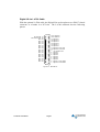
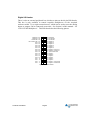
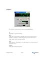
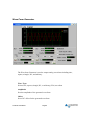
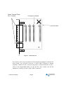
1
Acquitek CH Series High Speed Data Acquisition Boards for PCI Bus User Manual September 2006 Information in this document is subject to change without notice. © Copyright 2006, Acquitek, SAS. All rights reserved. Acquitek is a trademark of Acquitek, SAS. Other trademarks and trade names may be used in this document to refer to either the entities claiming the marks and names or their products. Acquitek, disclaims any proprietary interest in trademarks and trade names other than its own. Acquitek makes no warranty of any kind with regard to this material, including, but not limited to, the implied warranties of merchantability and fitness for a particular purpose. Acquitek shall not be liable for errors contained herein or for incidental or consequential damages in connection with the furnishing, performance, or use of this manual. Acquitek, SAS. 1 bis rue Marcel Paul, 91300 Massy France Acquitek CH Series High Speed Data Acquisition Boards for PCI Bus TABLE OF CONTENTS 1 INTRODUCTION ................................................................................................ 5 Features: ........................................................................................................................................6 CH Series Product Line: .................................................................................................................7 2 INSTALLATION................................................................................................... 8 CH Series Installation .....................................................................................................................8 3 HARDWARE OVERVIEW ..................................................................................10 Input Architecture .........................................................................................................................12 Output Architecture.......................................................................................................................15 Triggers ........................................................................................................................................17 Auxiliary Connections ...................................................................................................................18 Data Flow .....................................................................................................................................23 4 ACQUITEK CONTROL CENTER......................................................................25 Menu and Toolbar ........................................................................................................................26 System Tree Pane........................................................................................................................27 Configuration Pane.......................................................................................................................28 Info Tab ........................................................................................................................................29 Configuration Tab .........................................................................................................................30 Test Tab .......................................................................................................................................31 5 ACQUITEK BENCH ..........................................................................................32 Menu and Toolbar ........................................................................................................................33 DC Source ....................................................................................................................................35 Logic Analyzer ..............................................................................................................................36 Volt Meter .....................................................................................................................................39 Oscilloscope .................................................................................................................................41 Spectrum Analyzer .......................................................................................................................44 Strip Chart Recorder.....................................................................................................................46 Wave Form Generator..................................................................................................................48 6 THIRD PARTY DRIVERS ..................................................................................50 LabVIEW ......................................................................................................................................50 MATLAB .......................................................................................................................................52 TestPoint ......................................................................................................................................54 ExcelDA – Microsoft Excel Add-In................................................................................................56 DASYLab......................................................................................................................................61 CH-Series User Manual Page 3 7 TECHNICAL SPECIFICATIONS .......................................................................65 8 B-1350 CONNECTOR BOARD (OPTIONAL) ...................................................68 9 B-1250/1255 RF MULTIPLEXER (OPTIONAL) ................................................72 Architecture ..................................................................................................................................72 Connection ...................................................................................................................................73 Operation......................................................................................................................................77 Configuration ................................................................................................................................77 10 CABLES & CONNECTORS (OPTIONAL) ......................................................80 11 GLOSSARY.....................................................................................................83 12 TECHNICAL SUPPORT ..................................................................................88 CH-Series User Manual Page 4 1 Introduction The Acquitek CH Series of High Speed Data Acquisition Boards was designed to provide superior high-speed functionality and performance at a low price. All CH Series Boards utilize 16 MB of onboard memory, a local processor, and PCI bus mastering to provide glitch-free capture and/or playback of analog signals of length limited only by host RAM size, even with a non-realtime PC operating system. With multiple simultaneous inputs, dual simultaneous outputs, and excellent dynamic specifications, the CH Series boards are ideal for communications applications, such as IQ modulation and demodulation. With 12 bit resolution, high-speed precision and flexible triggering options, they are ideal for high-speed control applications. The onboard DSP coprocessor can offload intensive processing steps, such as FFTs, to free the host program for higher-level algorithms and applications. The outputs are full-featured arbitrary waveform generators with both waveform playback capability and function generation mode, and analog reconstruction filters on board. The board is PCI Plug-and-Play, and digitally calibrated, so there are no jumpers or potentiometers to manually adjust. CH-Series User Manual Page 5 Features: • Up to 4 input channels • Separate 40 MS/s A/D Converter per Channel • 12 Bit A/D Resolution • Up to 16 MB Local Acquisition Memory • Analog, Digital, Software Triggering Modes • 1 Hz A/D Sample Clock Resolution from onboard DDS • Up to 2 Output Channels with Arb/Function Generation Modes • Up to 40 MS/s D/A Converter per Channel • 12 Bit D/A Resolution • Analog Reconstruction Filtering • Up to 16 MB (64 MB optional) Local Waveform Memory • 1 Hz D/A Sample Clock Resolution from onboard DDS • • 16 Digital I/Os (Synchronous with Analog I/O) • 2 Counter/Timers • PCI Bus-Mastering Transfers at >80 MB/s sustained • Onboard 143 MHz, 32 Bit DSP for Numerical Coprocessing • Windows 98/ME/2000/XP, Linux Compatibility CH-Series User Manual Page 6 CH Series Product Line: CH-3160 CH-3150 4 analog inputs, 0 analog outputs, 50 Ohms 2 analog inputs, 2 analog outputs, 50 Ohms CH-3161 CH-3151 4 analog inputs, 0 analog outputs, 75 Ohms 2 analog inputs, 2 analog outputs, 75 Ohms CH-Series User Manual Page 7 2 Installation CH Series Installation To install the CH Series hardware and software, complete the following steps: Install the Acquitek Data Acquisition Hardware • • • • • Turn off your computer and disconnect the power cord. Locate a free PXI expansion slot. Carefully remove the card from its packaging. Insert the card into the PXI expansion slot and activate the latch Reconnect the power cord. Connect the Cables • Connect the IO cables to your external devices or breakout board. Install the Windows Device Drivers • • • • • • Turn on the computer. When Microsoft Windows boots, it should discover the new device and launch the New Hardware Wizard. Insert the Acquitek Data Acquisition Setup CD into your CD-ROM drive. Direct the New Hardware Wizard to search the CD-ROM drive for the device drivers. Windows may warn that the drivers are not authenticated. Proceed with installation. After the drivers are installed, remove the CD and reboot your computer. CH-Series User Manual Page 8 Install the Application Software and Third Party Drivers • • • • Insert the Acquitek Data Acquisition Setup CD into your CD-ROM drive. Run Setup.exe from the root directory of the CD Follow the onscreen instructions to install the application and driver software. It is recommended that you leave installation options unchanged to perform a full installation of all software components. After the installation completes, remove the CD and reboot your computer. Configure the Data Acquisition Hardware • • • • Run Acquitek Control Center from the Acquitek program group on the Windows Start menu. The new data acquisition device should appear as a node in the Local System | Hardware | Acquitek | PCI/PXI branch of the System tree. Click on the node. The serial number and logical device number will display in the Configuration pane. The logical device number is the tag that all application software uses to specify which hardware device will be used. To change the assigned device number, click on the configuration tab and select a new number using the device number edit control. Click the save button to make the change permanent. Test the Data Acquisition Hardware • • • If Acquitek Control Center is not still running, re-run the application from the Acquitek program group on the Windows Start menu and select the System tree node for the data acquisition device. Select the Test tab in the Configuration pane. The displayed test panels can be used to test all analog input channels and analog output channels as well as the digital IO lines. Connecting an analog output to an analog input, then turning on both panels can be used as a quick check to verify basic operation. Run Application Software • • • Installation and configuration of the Acquitek data acquisition hardware and software is now complete. You can run the included Acquitek Bench application software to use the device in a wide range of test and measurement tasks. Remember that all application software will refer to the data acquisition hardware using the logical number assigned by Acquitek Control Center. CH-Series User Manual Page 9 3 Hardware Overview Hardware Overview The Acquitek CH family of PCI data acquisition cards has the functionality of an oscilloscope, logic analyzer, function generator, and arbitrary waveform generator. The oscilloscope features two channels with software selectable high impedance inputs for light circuit loading or 501 Ohm inputs for minimum noise on small signals. The logic analyzer samples up to 16 inputs synchronously with the analog inputs. The signal generators can drive low distortion signals up to 10 Vpp into a 501 Ohm load. A memory controller with a large bank of onboard memory buffers both input and output signals from the PCI bus. This is critical, since even though the board can sustain bus master transfers at nearly 100 MBps across the bus, the net throughput of the board is up to 160 MBps and PCI activity could cause interruptions in the data streaming. Finally, an onboard digital signal processor (DSP) is used for real-time control of inputs, outputs, triggering, and to implement algorithm acceleration and real-time execution. The CH-3150 board is shown in figure 3-1a, with the major sections and connectors identified. A CH-3150/1 is fully populated with two inputs and two outputs. The CH-3160 board is shown in figure 3-1b. A CH-3160/1 features four inputs and no outputs. The control hardware, onboard processor, memory, and software interface are identical for the entire family of CH boards. 1 75 Ohms on CH-3131/41/51/61 boards CH-Series User Manual Page 10 Pin 1 Ain0 Analog Input Section Ain1 DIO Header FPGA Aux Aout0 Analog Output Section DSP/ PCI Interface SDRAM Aout1 Figure 3-1a – CH-3130/40/50 DIO Header Ain0 Ain1 Analog Input Section FPGA Ain2 DSP/ PCI Interface Ain3 SDRAM Aux Figure 3-1b – CH-3160 Board There are no manual adjustments or switches on the CH board. Calibration is performed at the factory, and the calibration settings are stored in an on-board EEPROM. The calibration settings are used to set digital gain and offset trimming potentiometers. Therefore, the calibration is performed in the analog domain, preserving the full dynamic range of the A/D and D/A converters and eliminating any processing overhead for software calibration. CH-Series User Manual Page 11 Input Architecture Two identical analog input chains drive a two channel, 12 bit analog-to-digital converter (A/D) on CH boards equipped with analog inputs. There is one clock for the A/D, ensuring that both channels are sampled simultaneously. The input channel is shown in figure 2. 0/7dB 1 MOhm 12 Bit A/D Converter ++ - 50 Ohms Gain/Offset Trim 1 MOhm Figure 3-2 – CH Input Architecture The signal is connected to the board through a BNC connector into a high speed instrumentation amplifier. This is a differential input amplifier, allowing the signal reference to be electrically isolated from the board ground. The purpose of this isolation is to prevent ground loops from occurring in the measurement setup. A typical ground loop setup is depicted in figure 3-3a. As can be seen from the figure, the measured voltage is in error by the amount of ground potential difference between the source and measurement device. This can be a major problem, preventing accurate measurements, particularly when the signal source is a long distance away from the measurement point, or the source and measurement devices are powered from different electrical circuits. In figure 3-3b, the CH differential input is shown. However, the voltage difference from the input reference to the local computer ground (Vgnd from figures 3-3a and 3-3b) should not exceed ±3.5 V. Any voltage difference will limit the available input range of the CH board. CH-Series User Manual Page 12 ++ - Vsignal ++ - Vgnd ++ - Vsignal + Vgnd Figure 3-3a - Ground Loop ++ - Vsignal ++ - Vgnd ++ - Vsignal Figure 3-3b - CH Differential Input Eliminates Ground Loop NOTE: The differential input structure of the CH is only intended to eliminate ground loops. With a balanced transmission medium, such as twisted pair wire, a differential input will also reject noise picked up on the transmission medium due to the symmetry of the noise between both differential inputs. However, with the coax connection typical for the CH input, noise will couple onto the coax shield, not the center conductor, and therefore the differential input may increase the amount of noise picked up on the transmission medium. If ground loops are not an issue in the CH application and excessive noise is being picked up on the coax, please contact the factory. A switchable termination resistor can be enabled to terminate the input. 50 Ohms is the nominal termination impedance. 75 Ohm termination for video applications is available. Please contact the factory for this option. CH-Series User Manual Page 13 An AC coupling capacitor can also be switched in line. The AC coupling can block up to 25 VDC. However, be extremely careful when measuring such signals with large DC offsets. If the AC coupling capacitor is switched out when connected to a signal with a large DC offset, the large voltage could damage the CH input circuitry. Signals larger than the ±12V from the board ground are potentially damaging to the CH board. A variable gain stage follows the input instrumentation amplifier. This stage provides sufficient low noise gain to allow a full-scale A/D input from an analog input signal of 100 mVpp, and attenuation to allow full-scale A/D input from an analog input signal of 10 Vpp. Following the variable gain stage is a buffer amplifier which drives the A/D. Note that there is no anti-aliasing filter preceding the A/D. This gives the user maximum flexibility with the signal input. There is a single pole noise limiting filter with a cutoff frequency of approximately 70 MHz just preceding the A/D. With that exception, there is no restriction on exceeding the Nyquist bandwidth at the selected sampling rate. The rest of the signal chain will operate up to 90 MHz, although harmonic distortion will be increased at higher input frequencies. The A/D converter is 12 bits. The A/D data format is two’s complement, as the CH family always operates in bipolar signal mode. In addition to the analog inputs, there are sixteen digital input/output (DIO) pins which can be sampled. The DIO’s must be set as input or output. The pins are divided into two 8 bit ports. All pins in each port must be set for the same direction. If a port is set as an output, the output state will be returned when the port is read. The DIO port can be sampled in two ways. A simple single reading mode which is asynchronous with the A/D clock is useful for signals which are not expected to change quickly. A clocked mode in which the DIO’s are sampled synchronously with the analog inputs and the data is streamed to host memory is also available. Due to data rate limitations, this mode is not available when the sample clock is over 10 MHz. In input mode, the DIO’s are pulled to +5V through a 10 K Ohm resistor. There is also a 100 Ohm software switchable termination resistor which can be used to improve signal integrity on high speed digital switching signals. CH-Series User Manual Page 14 Output Architecture There are two identical output channels on CH boards equipped with analog outputs. The output chain is depicted in figure 3-4. The analog output starts with a 12 bit digital to analog converter (D/A). The D/A on the CH board always operates bipolar mode; therefore, the data input format is two’s complement. 0/20 dB 0/6/14/20 dB 50 Ohms th 7 Order Filter Offset Trim 12 Bit D/A Converter Gain Trim Figure 3-4 – CH Output Architecture Following the D/A output buffer amplifier is an analog reconstruction (antialiasing) filter. This filter is a 7th order Butterworth low pass filter, with cutoff frequency of 8 MHz. A Butterworth response was chosen as the best compromise between frequency domain cutoff properties and time domain transient response. In the Acquitek software library, square and triangle waveforms are implemented. Their frequency is limited to 1 MHz so that the ringing which results from Gibbs Phenomena is kept to a minimum. In arbitrary waveform mode, it is recommended that the user keep the sample clock close to the maximum rate of 20 MHz in order to maximize the benefit of the onboard reconstruction filter. If a low frequency waveform is desired, digital interpolation can be used prior to loading the waveform. At the output of the reconstruction filter are two banks of switched attenuators. The first bank provides attenuation of 0 dB, 6 dB, 14 dB, and 20 dB. The second bank provides attenuation of 0 dB or 20 dB. Following the attenuation is the output high power amplifier. This amplifier is source terminated in 50 Ohms. 75 Ohm source termination for video applications is available. Please contact the factory for this option. The high power amplifier is capable of driving 10 Vpp into a 50 CH-Series User Manual Page 15 Ohm load, or 20 Vpp into a high impedance load. NOTE: The CH output amplifier depends upon the PC power supply for its +12V supply. While the PC +12V power is filtered before it is used to power the output amplifier, it is not stepped up with a switching supply. If the PC power supply does not provide 12V, the CH output may be clipped slightly below the 10V maximum output. Pay careful attention to the PC power supply if it is intended to operate the CH output at its maximum level, as some supplies may only provide 11.5V or less. With this maximum output drive capability and the analog attenuation ranges, the following full-scale output ranges are possible (all assuming a 50 Ohm load): 100 mVpp, 200 mVpp, 500 mVpp, 1 Vpp, 2 Vpp, 5 Vpp, 10 Vpp. CAUTION: With an unterminated load, the voltage delivered to the load will be twice that delivered to a terminated load (i.e. up to 20Vpp, or +/-10V). Be sure that this voltage will not damage the load. The output amplifier has a very low noise voltage level of 1.7 nV/sqrt(Hz). It operates at a gain of 10. At low signal levels when the 2nd stage 20 dB attenuator is active, the CH analog output delivers only -140 dBm/Hz into a 50 Ohm load, excluding D/A quantization noise. At higher levels, when the 20 dB attenuator is not active, the noise level increases to approximately –130 dBm/Hz. In addition to the two analog outputs, there are sixteen DIO’s which can be driven as outputs. The DIO’s must be set as input or output. The DIO pins are divided into two 8 bit ports. All pins in each port must be set for the same direction. Pins can be written in two ways. A simple single write mode which is asynchronous to the D/A clock is useful for outputs which do not change quickly. A clocked mode in which the DIO’s are driven synchronously with the D/A clock is also available. In this mode, the DIO’s share the output data with the Analog Output 1 channel D/A converter. The DIO output is driven through a 47 Ohm source termination resistor to improve signal integrity of high speed switched signals. CH-Series User Manual Page 16 Triggers The CH and XH series of boards support a variety of triggering options. Trigger sources are: Analog Input 0, Analog Input 1, External, Digital. The XH board also supports additional PXI triggers. See the “XH Series PXI Implementation” section of the manual. The Ain and External triggers support rising or falling edge triggering. There is also a hardware noise reject filter which requires the trigger to exceed the threshold for approximately one half microsecond before signaling the trigger event. This mechanism will introduce a delay in the trigger point of approximately one half microsecond, which may be an appreciable number of samples at high sample rates. Digital triggering supports either a pattern match mode, where all of the enabled digital trigger bits (up to 16) must match a predefined pattern, or edge mode, where a selectable rising or falling edge on any of the enabled digital trigger bits generates a trigger. Trigger sources are selected by software. See the Acquitek Data Acquisition SDK manual documentation for the set trigger functions. It should be noted that in addition to triggering an input capture, outputs can also be triggered from the above sources (i.e. analog output triggered by an analog input signal crossing a threshold). Not all possible combinations of functionality are possible. For example, the external clock and external trigger share a connector and circuitry, so it is not possible to use both simultaneously. CH-Series User Manual Page 17 Auxiliary Connections Auxiliary BNC Connector An auxiliary BNC connector is available for several functions. Only one of these functions is operable at any time. Software can select one of these modes: external analog trigger input, D/A waveform sync output, external clock input for the analog I/O channels, or external clock output synchronous with the A/D clock or D/A clock. The circuitry driving the auxiliary BNC connector is shown in figure 3-5. Output Enable D/A Sync Pulse Int Mx D/A Clk Int Nx A/D Clk 50 Ohms ÷N A/D Clk ÷M D/A Clk Ext Trig 100k Ohms +4V -4V Figure 3-5 – Aux BNC Architecture In input modes, the input is a high impedance input. As can be seen from figure 35, the input signal first passes through a high speed comparator. When set for external clock input, the comparator threshold is set for 1V. The input signal can be a square wave or sine wave, bipolar or unipolar. It should be limited to the range of ±5V. When set for external trigger input, the comparator voltage is set to the external trigger level. The external trigger level is limited to ±4V. CH-Series User Manual Page 18 In output modes, the signal is terminated in 50 Ohms, and will drive a D/A sync pulse or square wave clock at approximately 0 – 2 V into a 50 Ohm load, or 0 – 4 V into a high impedance load. The on-board circuitry for both analog input and analog output is clocked at an integer multiple of the actual sample rate. The external clock port on the board, whether taking in or driving an external clock, operates at the multiplied clock rate. The actual integer multiple varies. When using the internal clock, the multiple is completely handled by the Acquitek driver software transparently to the user. In external mode, it can not be completely transparent. Typically, the analog output clock runs at 4 times the sample rate in single channel mode or 2 times the sample rate in dual channel mode. The analog input clock typically runs at a high frequency, and the divide ratio is increased as the desired sample rate is decreased. In all cases, 80 MHz is the maximum frequency of the external clock. Refer to the Acquitek Data Acquisition SDK manual for details on setting the frequency when using external clock modes. Note that the signals on the CH board auxiliary BNC are high speed, and should be treated as such. Typically, 50 Ohm coaxial cable should be used to connect the output of the auxiliary BNC to its load. If it is being connected to another board or boards’ auxiliary BNC input, which is high impedance, BNC “T” connectors should be used, and the cable should be terminated in 50 Ohms after connection to the last auxiliary BNC in the chain. Counter/Timers The CH board has two hardware-based counter/timers. These counter/timers are based upon the 8254 functionality, and take in a clock and gate signal and generate an output signal. On the CH board, the clock sources are fixed: CT0 takes its clock from the analog input sample clock (i.e. not the integer multiple of sample clock as described in the auxiliary BNC section), while CT1 takes its clock from the analog output clock which is 2x or 4x the D/A clock depending upon whether one or two output channels are enabled. The gate source is either from a software register or from an input pin shared with the digital I/O. The output goes to a software register and can be directed to an output pin shared with digital I/O. See the digital I/O pinout drawings (figures 3-7, 3-8) for the specific pin information. CH-Series User Manual Page 19 The Acquitek Data Acquisition SDK has documentation on the functions used for programming the counter/timers. Use the SDK functions for setting the Ain and Aout clock to set the CT0 and CT1 frequencies, respectively. Note that the DIO port which contains the counter/timer output pins must be set to output mode for the counter/timer output to be driven on the pins. The DIO port which contains the counter/timer gate pins must be set to input mode for the gate signal to be read from the pins. Count is up to 24 bits, and is programmed with the number of clocks to be counted. The operating modes are: Mode 1: Retriggerable One Shot Out is high. Rising edge on gate triggers out to go low and down counting to start. Out stays low until count expires, at which point out goes high. Mode 2: Rate Generator Out is high. Gate high enables down counting. When count expires, out goes low for one clock cycle, then high again. Count is reloaded and down counting continues. This results in a sequence of negative pulses of width 1/clockFreq and period countReg/clockFreq being generated while gate is active. Mode 3: Square Wave Generator Out is high. Gate high enables down counting. When count reaches count/2, out goes low. When count expires, out goes high. Count is reloaded and down counting continues. This results in a square wave of approximately 50% duty cycle and period countReg/clockFreq being generated while gate is active. Mode 5: Retriggerable Strobe Out is high. Rising edge on gate triggers down counting to start. Out stays high until count expires, at which point out goes low for one clock, then high again. CH-Series User Manual Page 20 Digital I/O via L-4700 Cable With the optional L-4700 cable, the Digital I/Os are brought out to a DB-37 female connector as a header in a PCI slot. The L-4700 connector has the following pinout: B-1250 SD - 37 +5V Fused 0.75A - 36 Gnd - 35 Gnd - 34 Gnd - 33 Gnd - 32 Gnd - 31 Gnd - 30 Gnd - 29 Gnd - 28 Gnd - 27 Gnd - 26 Gnd - 25 Gnd - 24 Gnd - 23 Gnd - 22 Gnd - 21 Gnd - 20 19 - B-1250 CS 18 - B-1250 SC 17 - DigI/O 15 16 - DigI/O 14 15 - DigI/O 13 14 - DigI/O 12 13 - DigI/O 11 12 - DigI/O 10 11 - DigI/O 9 / Cntr1 Out 10 - DigI/O 8 / Cntr0 Out 9 - +5V Fused 0.75A 8 - DigI/O 7 7 - DigI/O 6 6 - DigI/O 5 5 - DigI/O 4 4 - DigI/O 3 3 - DigI/O 2 2 - DigI/O 1 / Cntr1 Gate 1 - DigI/O 0 / Cntr0 Gate Figure 3-7 - DI/O DB-37 CH-Series User Manual Page 21 Digital I/O Header There is also an external peripheral bus which uses pins on the 40-pin DIO header. This bus is only available to control Acquitek multiplexers via the Acquitek software toolkit. Up to eight external muxes, which can be used to mux the analog inputs or outputs, can be connected at one time. See Section 9 of this manual - “B1250/1255 RF Multiplexer”. This DIO header has the following pinout: Reserved - 40 Reserved - 38 B-1250 SD - 36 +5V Fused 0.75A - 34 Gnd - 32 Gnd - 30 Gnd - 28 Gnd - 26 Gnd - 24 Gnd - 22 Gnd - 20 Gnd - 18 Gnd - 16 Gnd - 14 Gnd - 12 Gnd - 10 Gnd - 8 Gnd - 6 Gnd - 4 Gnd - 2 39 - Reserved 37 - B-1250 CS 35 - B-1250 SC 33 - DigI/O 15 31 - DigI/O 14 29 - DigI/O 13 27 - DigI/O 12 25 - DigI/O 11 23 - DigI/O 10 21 - DigI/O 9 / Cntr1 Out 19 - DigI/O 8 / Cntr0 Out 17 - +5V Fused 0.75A 15 - DigI/O 7 13 - DigI/O 6 11 - DigI/O 5 9 - DigI/O 4 7 - DigI/O 3 5 - DigI/O 2 3 - DigI/O 1 / Cntr1 Gate 1 - DigI/O 0 / Cntr0 Gate Figure 3-8 - 40 Pin Header CH-Series User Manual Page 22 Data Flow The input data flow of the CH board is depicted in figure 3-9. The output data flow is depicted in figure 3-10. There are two performance features to note from these figures. First, when the input is set for triggered capture, the A/D converters are continually capturing data into the local SDRAM. When an enabled trigger event occurs, the local processor records the current sample number at the time when the trigger occurred. Until this happens, data is not transferred across the PCI bus. A large pre-trigger buffer is supported by the large bank of onboard SDRAM memory. Triggering is available from the following sources: analog level from either analog input channel or the external trigger with positive and negative slope, or on logical combinations of up to all sixteen DIO’s. Software can also trigger data capture or place the analog inputs into free run mode. A/D Local SDRAM FPGA PCI Bus Host SDRAM Analog Trigger Ext Trigger DIO Trigger S/W Trig (free run) Figure 3-9 – Input Data Flow Host SDRAM PCI Bus Local SDRAM FPGA D/A Sync Ext Trig Figure 3-10 – Output Data Flow CH-Series User Manual Page 23 D/A Also, note that input and output data is transferred as 16 bit words. This minimizes processor overhead which would be required to separate 12 bit A/D and D/A words if they were packed into 3 bytes. However, with 20 MHz * 2 bytes/sample * 2 channels = 80 Mbytes/sec on both the input and the output, net data throughput required of the CH board is 160 Mbytes/sec. The theoretical maximum for the PCI bus is only 132 Mbytes/sec, and even with a bus mastering controller on the CH, 100 Mbytes/sec is difficult to sustain due to other activity on the bus. In this case, the large onboard SDRAM memory bank is used to ease the PCI throughput bottleneck. In most cases, the output waveform will be loaded into onboard memory, and streamed to the D/A converters from there. As the waveform repeats, the D/A waveform sync can be driven out the auxiliary BNC connector. This frees the entire PCI bandwidth to support the 80 MByte/sec stream from the analog input channels. This mechanism is typical because a deterministic, repetitive output waveform is often sufficient to stimulate a test or measurement setup, while it is often desired to capture large amounts of input data for analysis. With the described implementation, a waveform stimulus of up to 8 million samples can be stored in the onboard memory, and input samples captured up to the amount of free RAM in the host computer system. CH-Series User Manual Page 24 4 Acquitek Control Center Acquitek Control Center (ECC) provides a central location for the configuration and test of data acquisition products from Acquitek . ECC is used to assign logical device numbers to Acquitek hardware devices so that those devices can be accessed from other software applications. ECC can also be used to specify default configuration parameters for Acquitek hardware devices and to verify correct installation and operation of those devices. CH-Series User Manual Page 25 Menu and Toolbar File / Load Profile Loads a previously saved set of configuration data, making those settings active. File / Save Profile Save the current configuration settings for all Acquitek devices to a named file. File / Exit Exit Acquitek Control Center Edit / Preferences Set general application preferences including whether to scan hardware and software each time Acquitek Control Center is started. View / Refresh Scan the system for installed hardware and software Help / Contents View help for Acquitek Control Center Help / Acquitek Web Site Open the Acquitek home page in a default browser window Help / About Display version and copyright information for Acquitek Control Center CH-Series User Manual Page 26 System Tree Pane The System Tree Pane displays a graphical representation of the hardware and software discovered during the last system scan. This information can be updated by selecting View / Refresh from the main menu. There are separate branches on the tree representing Acquitek hardware devices, system and third party hardware devices, Acquitek software components, OS software components, and third party software components. The leaves on the branches can be selected to display additional information in the Configuration Pane. CH-Series User Manual Page 27 Configuration Pane The Configuration Pane displays one or more tabbed pages with additional information about the hardware device or software module currently selected in the System Tree. CH-Series User Manual Page 28 Info Tab The information displayed on the Info Tab varies according to the device or module selected in the System Tree. Selected Acquitek hardware devices display their serial number and the configured device number. Other hardware devices display PCI configuration data. Software modules display version resource information if available along with file date and size. CH-Series User Manual Page 29 Configuration Tab The Configuration Tab is only available when an Acquitek hardware device is selected in the System Tree Pane. This page is used to set the logical device number for Acquitek devices to be used by other software applications. CH-Series User Manual Page 30 Test Tab The Test Tab is only available when an Acquitek hardware device is selected in the System Tree Pane. This page is used to test functionality of the selected device. Select a device channel for analog IO, or configure direction for digital IO, then activate the panel by clicking its 'On' button. Correct installation and operation can be verified for all analog and digital channels. CH-Series User Manual Page 31 5 Acquitek Bench Acquitek Bench is a collection of tools that enables a PC equipped with an Acquitek data acquisition device to function as a DC voltage source, a logic analyzer, a digital multimeter, an oscilloscope, a spectrum analyzer, a strip chart recorder, and an arbitrary wave form generator CH-Series User Manual Page 32 Menu and Toolbar The menu and toolbar are used to open and close the various instruments windows and arrange the display of those windows. File Exit Close Acquitek Bench Edit Preferences Set application specific preferences View DC Source Open or close the DC Source window Logic Analyzer Open or close the Logic Analyzer window Meter Open or close the Meter window Oscilloscope Open or close the Oscilloscope window Spectrum Analyzer Open or close the Spectrum Analyzer window CH-Series User Manual Page 33 Strip Chart Open or close the Strip Chart window Waveform Generator Open or close the Waveform Generator window Window Cascade Cascade all open child windows Tile Tile all open child windows Minimize All Minimize all open child windows Close Close the currently selected child window Help Contents Display help contents Acquitek Web Site Launch the default browser and direct to www.Acquitek.com About Display version and copyright information CH-Series User Manual Page 34 DC Source The DC Source is used to output a constant voltage on an analog output channel. Analog Out Channel Zero based analog output channel number. Device Number Data acquisition device number as configured in Acquitek Control Center. You must assign a device number to the acquisition board before it can be used in Acquitek Bench or other application software. CH-Series User Manual Page 35 Logic Analyzer The Logic Analyzer is used to capture and inspect logic level (0V - +5V) signals using the digital IO lines. SEC/DIV Specify the number of seconds per division on the Horizontal Axis Display Position (Time Base) Specify the vertical offset of the entire channel in percent of the Display. Pre-Capture Specify how much data to capture before the beginning of the display. The value is specified in divisions of the horizontal axis. CH-Series User Manual Page 36 Post-Capture Specify how much data to capture after the end of the display. The value is specified in divisions of the horizontal axis. Level Specify the level where the trigger mechanism will trigger a new frame to be displayed. Source Specify the channel index used as the data source by the Trigger. Slope Specify whether a positive or negative slope is used when triggering. Auto Specify whether the Trigger is Automatic or Manual. If this value is FALSE, then you must manually evaluate the Trigger by pressing the trigger button in the Trigger section of the Scope Panel. Volts/DIV Specify the number of volts per division on the vertical axis display. Position (Channel) Specify the vertical offset of the entire channel in Percent of the Display. Coupling Specify the signal coupling of this channel. Visible Specify whether the channel trace line is visible. Digital In Lines Digital inputs which will be sampled and displayed. Only the first 8 DIOs can currently be used. Samples / Second Input sampling rate. CH-Series User Manual Page 37 Device Number Data acquisition device number as configured in Acquitek Control Center. You must assign a device number to the acquisition board before it can be used in Acquitek Bench or other application software. Note: Additional configuration options can be accessed by right clicking on the instrument. CH-Series User Manual Page 38 Volt Meter The Volt Meter is used to measure voltages on analog input channels. AC Enable RMS AC signal measurement Range Voltage range of signal under test. Selecting 'Auto' will cause the volt meter to automatically determine the smallest range which encompasses the measured voltage, thereby yielding the highest precision. Mode Analog input type – differential (2 wire), single ended (1 wire), or non-referenced single ended (1 wire) Coupling Analog input coupling and impedance CH-Series User Manual Page 39 Analog In Channel Zero based analog input channel number Device Number Data acquisition device number as configured in Acquitek Control Center. You must assign a device number to the acquisition board before it can be used in Acquitek Bench or other application software. CH-Series User Manual Page 40 Oscilloscope The Oscilloscope is used to provide a two-dimensional visual display of an analog signal. Most commonly it is used to show signal amplitude versus time, displaying the waveform of the signal being monitored. SEC/DIV Specify the number of seconds per division on the Horizontal Axis Display Position (Time Base) Specify the vertical offset of the entire channel in percent of the Display. CH-Series User Manual Page 41 Pre-Capture Specify how much data to capture before the beginning of the display. The value is specified in divisions of the horizontal axis. Post-Capture Specify how much data to capture after the end of the display. The value is specified in divisions of the horizontal axis. Level Specify the level where the trigger mechanism will trigger a new frame to be displayed. Source Specify the channel index used as the data source by the Trigger. Slope Specify whether a positive or negative slope is used when triggering. Auto Specify whether the Trigger is Automatic or Manual. If this value is FALSE, then you must manually evaluate the Trigger by pressing the trigger button in the Trigger section of the Scope Panel. Volts/DIV Specify the number of volts per division on the vertical axis display. Position (Channel) Specify the vertical offset of the entire channel in Percent of the Display. Coupling Specify the signal coupling of this channel. Visible Specify whether the channel trace line is visible. CH-Series User Manual Page 42 Mode Analog input type – differential (2 wire), single ended (1 wire), or non-referenced single ended (1 wire) Coupling Analog input coupling and impedance Probe Specifies a 1x, 10x, or 100x probe for scaling of display values. Analog In Channel Zero based analog input channel number Device Number Data acquisition device number as configured in Acquitek Control Center. You must assign a device number to the acquisition board before it can be used in Acquitek Bench or other application software. Note: Additional configuration options can be accessed by right clicking on the instrument. CH-Series User Manual Page 43 Spectrum Analyzer The Spectrum Analyzer is used to measure the frequency spectrum of a signal on an analog input channel. Range Voltage range of signal under test Mode Analog input type – differential (2 wire), single ended (1 wire), or non-referenced single ended (1 wire) Coupling Analog input coupling and impedance CH-Series User Manual Page 44 Analog In Channel Zero based analog input channel number Samples / Second Input sampling rate. Device Number Data acquisition device number as configured in Acquitek Control Center. You must assign a device number to the acquisition board before it can be used in Acquitek Bench or other application software. CH-Series User Manual Page 45 Strip Chart Recorder The Strip Chart Recorder is used to capture and save voltage levels from the analog input channels. Range Voltage range of signal under test Mode Analog input type – differential (2 wire), single ended (1 wire), or non-referenced single ended (1 wire) Coupling Analog input coupling and impedance CH-Series User Manual Page 46 Probe Specifies a 1x, 10x or 100x probe for scaling of display values. Record Activate logging of data to disk File Name of data log text file. Each line of the file contains a time offset value followed by a tab, then the sample value and a carriage return Analog In Channel Zero based analog input channel number Samples / Second Input sampling rate. Device Number Data acquisition device number as configured in Acquitek Control Center. You must assign a device number to the acquisition board before it can be used in Acquitek Bench or other application software. Note: Additional configuration options can be accessed by right clicking on the instrument. CH-Series User Manual Page 47 Wave Form Generator The Waveform Generator is used to output analog waveforms including sine, square, triangle, DC, and arbitrary. Wave Type Selects sine, square, triangle, DC, or arbitrary (File) waveform Amplitude Sets the amplitude of the generated waveform Offset Sets a DC offset for the generated waveform CH-Series User Manual Page 48 WF File When File wavetype is chosen, selects the file containing waveform data. Each line of the file should contain a time offset value followed by a tab, then the sample value and a carriage return. Analog Out Channel Zero based analog output channel number. Frequency Output cycles per second. Waveform files are assumed to be 1024 points per cycle. Range Waveform amplitude min and max values. Device Number Data acquisition device number as configured in Acquitek Control Center. You must assign a device number to the acquisition board before it can be used in Acquitek Bench or other application software. CH-Series User Manual Page 49 6 Third Party Drivers LabVIEW The Acquitek Data Acquisition LabVIEW VIs provides a LabVIEW interface for all calls available through the Acquitek Data Acquisition API. The names and parameters are identical to those exported by XDADAQ.DLL. CH-Series User Manual Page 50 If the installation application was able to locate a LabVIEW installation on your computer, the Acquitek VIs have been installed into the LabVIEW directory and can be accessed from the LabVIEW function palette by choosing the Acquitek Data Acquisition palette view. If a LabVIEW installation was not detected, manual installation can be completed by copying the XDADaqLV and Menus directories from the [installdir]\ThirdParty\LabVIEW directory into the main LabVIEW installation directory (the directory containing LabVIEW.exe). A number of sample VIs are included and can be found in the [installdir]\ThirdParty\LabVIEW\Samples directory. These samples demonstrate wiring of the API level VIs and can also be used as higher level building blocks within new LabVIEW applications. The first time you attempt to open one of the samples from the [installdir]\ThirdParty\LabVIEW\Samples subdirectory, LabVIEW will not be able to find the XDADaqLV VIs used by the sample. You can either browse to the correct [LabVIEW_Install]\XDADaqLV\* directory using the 'find vi' dialog displayed by LabVIEW while loading the sample, or you can permanently fix the problem for all samples by opening the LabVIEW 'Tools / Options' menu, selecting 'Paths' and 'VI Search Path' then entering '[LabVIEW_Install]\XDADaqLV\*' and clicking 'Insert Before'. Note '[LabVIEW_Install]' should be replaced by the actual name of the directory where LabVIEW is installed on your system. Also note that the '\*' after XDADaqLV is needed so that LabVIEW will search the subdirectories under XDADaqLV. CH-Series User Manual Page 51 MATLAB Acquitek currently provides access to its data acquisition API in MATLAB via MEX-files. These functions are contained in .dll files in the \Acquitek\ThirdPary\MATLABMEX directory. Their help text documentation is contained in .m files with filenames that correspond to the .dll files. To see this documentation, type “help XXX" at the MATLAB prompt, where "XXX" is the part of the filename before the .dll extension, such as "XDA_Ain_Volts." The functions can be called just as any M-function is called. For example, to read a sequence of 5000 input voltages between -5V and 5V from analog input channels 0 and 1 of device 1 at 10000 Hz, type the following at the MATLAB prompt: [ch0 ch1] = XDA_Ain_Volts(1, [0 1], [5.0 5.0], 10000, 5000) CH-Series User Manual Page 52 The \Acquitek\ThirdPary\MATLABMEX directory currently contains MEX-files for analog input and output, digital input and output, and counter/timer functions. The analog input functions can be found in the following files: XDA_Ain_Coupling.dll XDA_Ain_Raw.dll XDA_Ain_Volts.dll Analog output functions can be found in the following files: XDA_Aout_Func.dll XDA_Aout_Raw.dll XDA_Aout_Volts.dll Digital input and output functions can be found in the following files: XDA_Din_Read.dll XDA_Dout_Write.dll Counter/timer functions can be found in the following files: XDA_CT_Config.dll XDA_CT_Gate.dll XDA_CT_Read.dll Example M-functions that use these MEX-files can be found in the \Acquitek\ThirdPary\MATLABMEX\Samples directory. CH-Series User Manual Page 53 TestPoint Capital Equipment Corporation’s TestPoint is software for designing test, measurement, and data acquisition applications. The Acquitek TestPoint driver enables the use of all Acquitek hardware with TestPoint to simplify data acquisition. CH-Series User Manual Page 54 Installation • • • Copy the file TPAcquitek.dll from [AcquitekInstallDirectory]\ThirdParty\TestPoint to the directory where TestPoint is installed. Edit the TestPoint.ini file found in the TestPoint directory. Replace the entire [AD0] section with this text: [AD0] manufacturer=AUTO MODE=Bipolar TYPE=Pseudo COUPLING=DC DACOUPLING=DC Edit the TPAD.ini file found in the TestPoint directory. Find the [ADDRIVERS32] section and add this line: ACQUITEKWDM=TPACQUITEK.DLL The Acquitek data acquisition board assigned logical device number one using Acquitek Control Center can now be accessed in TestPoint as AD device zero. To use multiple boards, or change the logical device that will be used, copy the board configuration information added for [AD0] into another section ([ADn]). The Acquitek device number will always be one greater than the TestPoint AD number. Notes You must run Acquitek Control Center to assign logical device numbers to all Acquitek devices and verify basic functionality before using the devices with TestPoint. The TestPoint driver will be copied to the [AcquitekInstallDirectory]\ThirdParty\TestPoint directory by Acquitek Setup. You must complete the installation as documented above. A sample TestPoint application called AD_DA.tst is copied to [AcquitekInstallDirectory]\ThirdParty\TestPoint\samples by Setup. This application can be used to verify basic functionality. CH-Series User Manual Page 55 ExcelDA – Microsoft Excel Add-In ExcelDA is a Microsoft Excel Add-In that enables data acquisition from within Excel using any Acquitek hardware device. It is included with all Acquitek products and installed into the ThirdParty directory when Acquitek Data Acquisition Setup is run. Installation To Install ExcelDA follow these steps: • • • • • • • • Start Microsoft Excel Choose 'Add-Ins...' from the Excel 'Tools' menu Click the 'Browse...' button on the Add-Ins dialog Navigate to [AcquitekInstallDirectory]\ThirdParty\ExcelDA Double click ExcelDA.xla Click the 'OK' button on the Add-Ins dialog Choose 'ToolBars' from the Excel 'View' menu Select 'Acquitek Data Acquisition' from the ToolBars list Once you have completed these steps, the Acquitek Data Acquisition toolbar will be available for use with any workbook within Excel. You can drag and dock the toolbar to a convenient spot on the Excel toolbar, or let it float within the work area as you prefer. CH-Series User Manual Page 56 General Configuration Display the General Configuration tab on the configuration dialog by clicking 'Configure' on the Acquitek Data Acquisition toolbar, then choosing the 'General' tab. Device Number Logical device number of the Acquitek hardware device that will be used for acquisition. This number must be assigned in Acquitek Control Center. Target Workbook The workbook to which data will be acquired. You must provide the entire name including the .xls extension if one is present. Target Worksheet The worksheet to which data will be acquired. This sheet must already be present in the specified workbook. Target Column Starting Column for data acquisition. Data for a single channel will be captured to the specified column. Data for multiple channels will be captured to consecutive columns. Target Row Starting row for data acquisition. Samples for each channel will be captured in consecutive rows starting with the specified row. CH-Series User Manual Page 57 Analog In Configuration Display the Analog In Configuration tab on the configuration dialog by clicking 'Configure' on the Acquitek Data Acquisition toolbar, then choosing the 'Analog In' tab. Channel Count The number of channels from which data will be acquired. Sample Count The number of samples to acquire from each channel. Note that Excel limits this value to about 65000. Sample Rate The sampling clock frequency to be used for the acquisition. Scan Rate The time between channel sample sets when using hardware that does not support simultaneous sampling. Set this value to 0 when acquiring one channel or when you wish to use the frequency specified by 'Sample Rate'. Range The maximum voltage of the input signal. Valid values for this parameter depend on the particular hardware device being used. Please see the hardware reference manual for a list of valid values. CH-Series User Manual Page 58 Polarity Input signal polarity - Bipolar or Unipolar. Coupling Input signal coupling - AC, DC, or DC Terminated. Mode Input signal mode - Differential, Single Ended, or Pseudo Differential. Trigger Channel Analog channel used to trigger acquisition. Trigger Level Voltage level at which data acquisition will trigger. Trigger Type Trigger mode - Falling, Rising, External, or None. To begin acquisition as soon as the 'Acquire' toolbar button is clicked, set this value to none. Trigger Noise Reject Enable Trigger Noise Reject to avoid triggering on noise from the trigger input signal. CH-Series User Manual Page 59 Acquisition Once all data acquisition parameters have been set using the configuration dialog, simply click the 'Acquire' button on the Acquitek Data Acquisition toolbar to acquire data directly into your Excel spreadsheet. If you have specified a non-existent target for acquisition, or your configuration parameters are otherwise incorrect, an error message will be displayed. You can then click 'Configure' again to display the configuration dialog and correct the problem. CH-Series User Manual Page 60 DASYLab DASYLab is an easy-to-use, Windows-based graphical data acquisition software package with which you build data acquisition and control applications more quickly. By using an icon-based flowchart, you develop your application with point-and-click ease -- no programming required. Installing the Acquitek DASYLab® Driver 1. Copy XDADASY.dll from the [installdir]\ThirdParty\DASYLab folder (most likely C:\Program Files\Acquitek\ThirdParty\DASYLab) to DASYLab's root folder (most likely C:\Program Files\DASYLab). CH-Series User Manual Page 61 2. Open DASYLab. 3. Choose Select Driver... from the Experiment menu in DASYLab. 4. Find XDADASY.dll in this dialog box. Highlight it and click OK. If XDADASY.dll does not show up in this dialog, the file may be in the wrong place. Make sure you have completed step 1 correctly. 5. DASYLab will inform you that you must restart DASYLab for the changes to take effect. Restart DASYLab. The Acquitek DASYLab Driver should now be installed and can be accessed from the Input/Output item in the Modules menu. Adding Acquitek Driver Modules to your DASYLab Worksheet To add modules using the Acquitek DASYLab driver to your worksheet, select Analog Input, Analog Output, Digital Input, or Digital Output from the Input/Output submenu of the Modules menu. Selecting a Device To choose a device, select “Hardware Setup” from the Experiment menu. Choose a device number (as defined in Acquitek Control Center) and click OK. CH-Series User Manual Page 62 Setting up Triggering To set up analog input triggering (CM/XM or CH/XH) or analog output triggering (CH/XH), select “Hardware Setup” from the Experiment menu. Select trigger options from the dialog box. To set up digital trigger mode, click the “Set up digital trigger” button and specify a port, mode, and which lines to enable. If you select Edge trigger, the bottom row of checkboxes allows you to specify which ports require a rising edge and which ports require a falling edge. If you select Pattern trigger, you can specify which ports will be logic high in the pattern and which ports will be logic low. CH-Series User Manual Page 63 Setting Input Channel Options To set coupling or input mode, double-click on an analog input module. In the dialog box that opens, select the channel you wish to set up and click “Channel Setup”. Specify options for each of these and click OK. For More Information For more information, please consult the DASYLab User Guide. CH-Series User Manual Page 64 7 Technical Specifications Analog Inputs Number of Inputs: Impedance: Coupling: Analog Bandwidth: Resolution: Full Scale Input Range: Absolute Max: Common Mode Range: CMRR: Gain Accuracy: Zero Accuracy: DNL: INL: SNR: SFDR: Triggering: Source: Levels: Slope: External: Sample Rate: Internal Clock: CH-Series User Manual CH-3150: 2 (synchronous) CH-3160: 4 (synchronous) 1M Ohm or 50 Ohm (75 Ohm available) Software Selectable AC or DC (Software Selectable) 70 MHz (-3 dB) 12 Bits ±50mV, ±100mV, ±200mV, ±500mV, ±1V, ±2V, ±5V Software Selectable ±12 V ±3.5 V 46 dB (at DC) ± 0.1 dB relative to full scale (at 100kHz) 0.1% of range +/- 1mV (at DC) < 1 LSB (monotonic) < 4 LSB 64 dB (500 kHz input, 1Vpp range) 60 dB (1Vpp range) Any Ain Channel, Ext, S/W, Dig I/O ±4V, 256 Steps + or – ±4V,100k Ohm Zin, 50 ns min Pulse width 10kHz – 10MHz (1Hz resolution) quad channel 10kHz – 20MHz (1Hz resolution) dual channel 10kHz - 40MHz (1Hz resolution) single channel Software Selectable Independent from output clk Page 65 External Clock: Memory: PCI Interface: Analog Outputs Number of Outputs: Impedance: Coupling: Analog Filters: Resolution: Full Scale Output Range: (into matched load) Gain Accuracy: Zero Accuracy: DNL: INL: SNR: SFDR: Triggering: Source: Ext Level: Ext Slope: Ext Input: Sample Rate: Internal Clock: External Clock: CH-Series User Manual Must be >=4x sample rate 100k Ohm Zin, 80 MHz max 16 MB (64MB option) local capture memory (shared with output memory) 32 bit, 33 MHz Bus Mastering (Continuous full speed capture of 2 chan at 20MSps per chan (80 MB/s) to PC memory is supported) CH-3160: 0 CH-3150: 2 (synchronous) 50 Ohm (75 Ohm available) DC 7th Order Butterworth, 8 MHz 3 dB Frequency 12 Bits ±50mV, ±100mV, ±200mV, ±500mV, ±1V, ±2V, ±5V Software Selectable ± 0.1 dB relative to full scale (at 100kHz) 0.1% of range ± 1mV (at DC) < 1 LSB (monotonic) 1 LSB 72 dB (500 kHz output, 1Vpp range) 55 dB (1Vpp range) Any Ain Channel, Ext, S/W, Dig I/O ±4V, 256 Steps + or – ±4V,100k Ohm Zin, 50 ns min Pulse width 1Hz – 20MHz (1Hz resolution) dual channel Up to 40 MHz single channel Software Selectable Independent from input clk Must be >=4x sample rate 100k Ohm Zin, 80 MHz max Page 66 Memory: Operating Modes: Sync Output: Digital I/O Number of I/O: Input High: Input Low: Output High: Output Low: Power Up State: Counter/Timers: Number: Clock: Speed: Modes: up to 16 MB (64 MB option) local waveform memory Arbitrary Waveform with Automatic looping Function (sine, square, triangle) Software enabled TTL compatible, 50 Ohm Zout 1 sample duration at segment boundary 16 (two 8-bit ports). Each port selectable as input or output 2.0 V, 5 V max 0.8 V, 0 V min 2.4 V min @ 24 mA 0.4 V max @ 24 mA Input (High Impedance) 2 (24 bits) Internal from A/D or D/A clk 80 MHz Max 8254 modes 1, 2, 3, 5 Physical/Environmental Dimensions: 7.15 in x 4.20 in 182 mm x 107 mm Power Consumption: 1.75A at +5V 0.5A at +12V Operating Temperature: 0°C to 55°C Storage Temperature: -20°C to 70°C Connectors: 5 BNC Female (CH-3130/40/50: 2 In, 2 Out, 1 Ext trig/clk/sync out) (CH-3160: 4 In, 1 Ext trig/clk) 40 Pin Header (digital I/O) 32 Bit PCI CH-Series User Manual Page 67 8 B-1350 Connector Board (Optional) The Acquitek B-1350 is an easy to use accessory which simplifies user connection to the sixteen digital input/output (DI/O) pins on the CH-Series PCI data acquisition boards. The B-1350 plugs into an empty expansion slot in a computer chassis. It makes no connection to the slot connector, so the slot can be either PCI or an ISA. The included 40-conductor ribbon cable connects from the CH board to the B-1350 via 40 pin, 0.100” spaced headers. The B-1350 has multiple headers for use with a variety of Acquitek boards; when using with a CH-Series board, connect to the header labeled CH DI/O as shown in Figure 1 below. The conductor labeled as Pin 1 on the ribbon cable (usually marked in red) should be connected to Pin 1 of the header, marked with a large dot on the B-1350 board. This same conductor should be connected to Pin 1 of the DI/O header on the CH-Series board, shown in Figure 2 below. CH-Series User Manual Page 68 Screw Terminal Plugs Pin 1 Location CH Digital I/O Header Loop Out Header Figure 1 – B-1350 Layout If you plan to also use an Acquitek B-1250 external RF multiplexer with the CHSeries board, you will have received a L-4700 (DB-37 Bracket to Header assembly) with the B-1250. After the steps above, connect the header of the L4700 to the Loop Out header on the B-1350, then connect the B-1250 multiplexer, as always, to the L-4700’s DB-37 connector. CH-Series User Manual Page 69 Analog Input Section DI/O Header Ain0 Ain1 FPGA Aux Analog Output Section Aout0 DSP/ PCI Interface Aout1 Figure 2 – CH Board Layout CH-Series User Manual Page 70 SDRAM DI/O Header Pin 1 Location The pinout of the screw terminal plugs is shown below. Note that the screw terminal plugs are removable to simplify the connection of wires. DI/O 0 DI/O 1 DI/O 2 DI/O 3 DI/O 4 DI/O 5 DI/O 6 DI/O 7 DI/O 8 DI/O 9 DI/O 10 DI/O 11 DI/O 12 DI/O 13 DI/O 14 DI/O 15 NC Gnd +5V Figure 3 – B-1350 Pinout CH-Series User Manual Page 71 9 B-1250/1255 RF Multiplexer (Optional) The Acquitek B-1250 is a 4:1, high frequency analog multiplexer/ demultiplexer (the B-1255 is the same unit without a physical enclosure). It is intended to operate under software control in conjunction with an Acquitek CH or XH Series high speed analog I/O board. The signal path is passive, so the mux is bidirectional (i.e. it can be used on either the inputs or outputs of the CH or XH board). The control interface utilizes a non-volatile configuration identity so that up to eight B-1250s can be controlled by a single CH or XH board. The low loss and excellent gain flatness allow cascading of several B-1250s with no significant signal degradation. Architecture A block diagram of the B-1250 is shown in figure 9-1 below. Four bi-directional mux terminals can be connected to a single common terminal. Mux terminals not connected to the common terminal are resistively terminated. Nominal termination resistance is 50 Ohms. Contact the factory for a 75 Ohm version. Switching elements are mechanical relays for low loss and excellent gain flatness. They are non-latching relays, so while powered down, on power up, and prior to the first software switch command, all mux terminals are terminated and the common terminal is open. CH-Series User Manual Page 72 DB-9 Control Interface 4 COM Rterm Rterm Rterm Rterm Figure 9-1 – B-1250 Block Diagram Connection Up to eight B-1250 multiplexers can be controlled by one CH board. In the tree configuration shown in figure 9-2, this allows up to 26 inputs to be muxed into the CH-3150 board. Note also that the B-1250 is bi-directional. The same type of tree configuration allows expansion for driving up to 26 outputs from a CH-3150 as shown in figure 9-3. With a CH-3160 board, up to 28 inputs can be muxed into the CH board as shown in figure 9-4. CH-Series User Manual Page 73 B-1250 ID=0 1 2 3 4 B-1250 ID=1 COM 1 2 3 4 B-1250 ID=2 COM 1 2 3 4 COM Ain0 B-1250 ID=3 Ain1 1 2 3 4 COM CH-3140/50 Aout0 Aout1 B-1250 ID=4 1 2 3 4 B-1250 ID=5 COM B-1250 ID=7 B-1250 ID=6 1 2 3 4 COM 1 2 3 4 COM 1 2 3 4 COM Figure 9-2 – CH-3140/50 Expansion to 26 Inputs Using Multiple B-1250 B-1250 ID=0 1 2 3 4 B-1250 ID=1 COM 1 2 3 4 B-1250 ID=2 COM 1 2 3 4 COM Ain0 B-1250 ID=3 Ain1 1 2 3 4 COM CH-3130/50 Aout0 Aout1 B-1250 ID=4 1 2 3 4 B-1250 ID=5 COM B-1250 ID=7 B-1250 ID=6 1 2 3 4 COM 1 2 3 4 COM 1 2 3 4 COM Figure 9-3 CH-3130/50 Expansion to 26 Outputs Using Multiple B-1250 CH-Series User Manual Page 74 B-1250 ID=0 B-1250 ID=1 1 2 3 4 COM B-1250 ID=2 1 2 3 4 1 2 3 4 COM Ain0 B-1250 ID=3 COM Ain1 Ain2 1 2 3 4 CH-3160 Ain3 COM B-1250 ID=4 B-1250 ID=5 1 2 3 4 COM 1 2 3 4 COM B-1250 ID=6 B-1250 ID=7 1 2 3 4 COM 1 2 3 4 COM Figure 9-4 CH-3160 Expansion to 28 Inputs Using Multiple B-1250 The control signals for the B-1250 are located on the 40 pin DIO header on the CH board. Connection of the B-1250 to the CH board depends upon whether the B1050 DIO breakout board will be used in the system. Figures 9-5 and 9-6 illustrate the cables and connections required to use the B-1250 with and without the B-1050 digital I/O breakout board. The figures show a CH-3150, but the cable requirements are common to the entire CH board family. CH-Series User Manual Page 75 L-480x B-1050 D B37 L-4700 D B9 L-489x Control Out 1 2 3 4 Control In L-489x COM Ain0 Ain1 B-1250 ID=0 CH-3150 Aout0 (CH-3151) Aout1 Control In L-420x (L-421x) 1 2 3 4 COM Notes •X denotes length in meters •CH-3151 is 75 Ohm version •L-421x 75 Ohm coaxial cables B-1250 ID=1 L-420x (L-421x) recommended with CH-3151 Figure 9-5 – B-1250 Connection to CH with B-1050 DIO Breakout L-4700 L-489x Control Out 1 2 3 4 Control In L-486x COM Ain0 Ain1 B-1250 ID=0 CH-3150 Aout0 (CH-3151) Aout1 Control In L-420x (L-421x) 1 2 3 4 COM Notes B-1250 ID=1 L-420x (L-421x) •X denotes length in meters •CH-3151 is 75 Ohm version •L-421x 75 Ohm coaxial cables recommended with CH-3151 Figure 9-6 – B-1250 Connection to CH without B-1050 DIO Breakout CH-Series User Manual Page 76 Operation The mux position can be set via software command from the Acquitek Data Acquisition SDK. See the Acquitek Data Acquisition SDK manual for details of the software commands. A visible LED indicates a currently active BNC connector. Because the switching elements are mechanical relays designed for low loss switching of RF signals, no calibration data is required to be read from or stored in the B-1250. Also due to the mechanical nature of the switching, the switching time and switch lifetime specifications should be considered as a part of the system integration of the B-1250. Configuration Before using multiple B-1250s in a system, a configuration step must be performed. All B-1250s are shipped with a factory default configuration ID of 0. Up to eight B-1250s can be controlled from a single Acquitek CH or XH board. Each of the B-1250s controlled by the same board must have a unique configuration ID. The configuration step entails a one time operation of connecting a single B-1250 to a CH or XH board and running a simple program to store the configuration ID in the B-1250 non-volatile memory. This program is called B1250Cfg.exe, and is included in the root directory of the Acquitek Data Acquisition Setup installation (\Acquitek\Util directory). Procedure NOTE: Only a single B-1250 can be connected to the CH or XH board during the configuration step. Connect a SINGLE B-1250 to the CH board as shown in either figure 9-4 or 95 depending upon whether a B-1050 DIO breakout board is used. The cable MUST be connected to the DB-9 connector on the B-1250 labeled “Control In”. Start the B1250Cfg application. It should appear similar to the screen shot in figure 9-7 below CH-Series User Manual Page 77 Figure 9-7 – B1250Cfg Main Screen Use the CH Device Number spin edit control to select the CH or XH board to which the B-1250 is connected. Assign the configuration ID by selecting the appropriate B-1250 ID radio button. Ensure that all B-1250s to be connected to the same CH or XH board are assigned a unique configuration ID. This step automatically stores the configuration ID in the B-1250 non-volatile memory. Test the connection by switching the mux position with the Channel radio button. Exit the B1250Cfg application. CH-Series User Manual Page 78 B-1250 Specifications DC Parameters Maximum I/O Voltage Maximum I/O current On resistance Termination resistance 30 V max 0.5 A max 100 mOhms 50 Ohms +/- 1% (Contact factory for 75 Ohm version) AC Parameters Insertion loss Gain Flatness Off Isolation < 0.05 dB at 1 MHz < 0.1 dB DC to 10 MHz >55 dB at 10 MHz Physical Switching time Switch cycles Power consumption Size Connectors CH-Series User Manual 10 ms max 300,000 operations while meeting full electrical specs 1,000,000 operations mechanical lifetime 20 mA at 5V (No terminals enabled) 70 mA at 5V (One terminal enabled) 7.2 x 5.528 x 1.52 inches (in box with connectors) 183 x 141 x 39 mm 7.2 x 5.28 x 0.58 inches (board only with connectors) 183 x 134 x 15 mm 4 BNC bi-directional multiplexed terminals 1 BNC bi-directional common terminal DB-9 for power and control input DB-9 for power and control daisy chaining Page 79 10 Cables & Connectors (Optional) Acquitek offer a wide array of breakout boxes, connector panels, cables and cable assemblies to assist in making analog and digital I/O connections to the CH Series boards. Available connectivity options include: B-1050 Breaks out digital I/O channels for CH Series. Requires L-4700 37-pin header and L-480x series cable. B-1055 Same as above, but without enclosure. B-1250 Four to One RF multiplexer for CH Series. Also available without enclosure (B-1255). Requires L-4700 37-pin header and L-486x series cable or B-105x and L-489x series cable. B-1410, B-1420 B-1410 is the Rackmount kit and termination panel for CH Series. B-1420 is the BNC termination panel for the B-1410. CH-Series User Manual Page 80 B-1350 PCI board providing easy screw-terminal header access to the 16 Digital I/O channels of the CH Series. Can be used instead of B-1050 breakout unit. L-4700 DB37 bracket to header connector. Used in conjunction with L-480x series cables to connect B105x digital I/O breakout units and/or B-125x RF multiplexers to CH Series board. L-4801, L-4802 Connects from DB37 connector of L-4700 to B-105x. Available in 1M (L-4801) and 2M (L-4802) lengths. L-420x, L-421x BNC to BNC cables, available in 50 Ohm (L-420x) and 75 Ohm (L-421x) configurations, and in 1m and 2m lengths. L-422x BNC to clip cables, available in 1m and 2m lengths. L-486x DB37 to DB9. Used to connect from L-4700 to B1250. Available in 1m and 2m lengths. CH-Series User Manual Page 81 L-489x DB9 to DB9. Used to connect from B-1050 to B-1250 or to daisy chain B-1250. Available in 1m and 2m lengths. The complete line of breakout boxes and cables is as follows: Breakout Boxes & Connector Boards B-1050 B-1055 B-1250 37-pin breakout. Breaks out digital I/O for CH boards. Requires L-4700 37-pin header and either L-480x cables or L-482x cables Same as above, but without enclosure 4 to 1 RF multiplexer for use with CH boards. Requires L-4700 37-pin header and either L-480x cables or L-482x cables B-1255 B-1350 Same as above, but without enclosure B-1410 B-1420 Rackmount kit: front panel and 2 empty hole covers (use with any of the boxes above) Header bracket with screw terminals, breaks out digital I/O for CH boards. Can be used instead of B-105x 37-pin breakout units. BNC termination panel for B-1410 Rackmount kit Cables L-4201 L-4202 L-4211 L-4212 L-4221 L-4222 L-4230 L-4700 BNC 50 Ohm -1m L-4801 DB37 Ext 1m: Connects from DB37 connector on L-4700 to one B-105x 37-pin breakout unit or one B-125x RF multiplexer unit. L-4802 DB37 Ext 2m: Connects from DB37 connector on L-4700 to one B-105x 37-pin breakout unit or one B-125x RF multiplexer unit. L-4861 DB37 to DB9 1m: Connects from DB37 connector on L-4700 to one B-125x multiplexer L-4862 DB37 to DB9 2m: Connects from DB37 connector on L-4700 to one B-125x multiplexer L-4891 DB9 to DB9 1m: Connects from DB9 connector on B-105x breakout unit to one B-125x multiplexer, or to daisy chain between two B-125x multiplexers. L-4892 DB9 to DB9 2m: Connects from DB9 connector on B-105x breakout unit to one B-125x multiplexer, or to daisy chain between two B-125x multiplexers. CH-Series User Manual BNC 50 Ohm - 2m BNC 75 Ohm - 1m: Use with 75 Ohm CH boards BNC 75 Ohm - 2m: Use with 75 Ohm CH boards BNC to clip 1m BNC to clip - 2m BNC to Scope Probe DB37 Bracket to Header: Used in conjunction with L-480x cables or L-482x cables to connect B-105 37-pin breakout units and/or B-125x RF multiplexers to CH and CM series boards Page 82 11 Glossary Aliasing - The term used to describe the observed effect of sampling an analog signal at a sampling frequency less than two times the highest frequency content of the signal. Signal processing theory, specifically Nyquist’s Theorem, states that an analog signal can be exactly reconstructed from a periodic sampling of that signal if the sampling rate is greater than twice the highest frequency contained in the analog signal. With the exception of some specialized undersampling applications it is important to prevent aliasing before it happens through the use of high sampling rates and/or anti-aliasing filters. Once a signal has been corrupted by aliasing, it can no longer be exactly reconstructed from its samples. Anti-Aliasing filter - A filter with a frequency cutoff below one half the sampling rate. It is used to prevent aliasing during the sampling of an analog signal. A/D – Analog to digital converter. A component which produces a digital representation of the voltage of an input analog signal at an instant in time called the sample time. Typically an A/D will sample an input signal periodically at a rate called the sample frequency. Bessel filter – A type of filter which has excellent time domain distortion properties (i.e. pulse response with very little ringing) but poor frequency domain cutoff properties. This filter characteristic can be implemented in either the analog or digital domain. Butterworth filter – A type of filter which has a good compromise between frequency domain cutoff properties and time domain distortion such as “ringing”. This filter characteristic can be implemented in either the analog or digital domain. Charge Injection – An undesirable property of a multiplexer in which a small amount of electrical charge is injected into the selected multiplexer input when the multiplexer switches. A voltage error is introduced which is equal to the injected charge divided by the input capacitance. The voltage error decays over time as a function of the source resistance. Lower source resistance results in faster decay of the voltage error. CMRR – Common Mode Rejection Ratio. See common mode range. CH-Series User Manual Page 83 Common Mode Range – With a differential voltage, the relevant measurement is the difference in voltage between the two signals in the pair. The absolute voltage between either signal and ground should not affect the differential measurement. In practice, voltages between the differential signals and ground can distort the differential measurement. Common mode rejection ratio (CMRR) is a measure of how much the voltage between the differential pair and ground distorts the differential measurement. The common mode range defines how large the voltage between either signal and ground can be before the differential inputs no longer function. D/A – Digital to analog converter. A component which produces an analog output signal which is proportional to a digital input value. Typically a D/A will hold the same analog output voltage for a period of time called the sample time, and be updated periodically with digital input values at a rate called the sample frequency. dB – A decibel, or dB, is 10 * log10 (power ratio between to signals). Since power is proportional to voltage squared, when dealing with voltages a dB is 20 * log10 (voltage ratio). dBfs – dB relative to a full scale A/D or D/A signal dBV – dB relative to one Volt. dBm – dB relative to one milliWatt. dBmV – dB relative to one milliVolt. Differential Input - An input through which the difference of two signals at the positive and negative inputs is measured rather than the difference between a signal and system ground. There is a limit to how far the two signals can be from the system ground before the input is no longer able to measure simply the difference between the two inputs but instead is distorted by the difference between the signals and ground. This limit is called the common mode voltage range. Elliptic Filter - A type of filter which has excellent frequency domain cutoff properties but poor time domain distortion properties (i.e. pulse response with excessive ringing). This filter characteristic can be implemented in either the analog or digital domain. FFT – Fast Fourier Transform. A mathematical tool for analyzing the frequency content of a signal. FIFO – First In, First Out. A temporary storage memory with no addressing in which data is stored and retrieved in first in, first out order. On a data acquisition board, a FIFO is used to free the host processor from servicing the data acquisition hardware on a periodic interval. Typically, the hardware accesses one side of the FIFO at the periodic sample rate (or a multiple of it). The host accesses the other side of the FIFO to either fill it with data for output or read the input data. The host can do so in burst mode, which is much more efficient. For example, a burst transfer across the host PCI bus can reach nearly 132 Mbytes/sec whereas non-burst transfers are a small fraction of that rate. With a non-realtime operating system such as Windows, it is important for the FIFO to hold enough data to sustain periodic data acquisition during intervals when the processor is not available to service the data acquisition hardware. CH-Series User Manual Page 84 Floating Source – A voltage source in which the voltage at the positive or negative terminal is referenced only to the other terminal, not to an absolute reference or ground. Batteries and thermocouples are common floating sources. Gibbs Phenomena – Signals with sharp edges in their time domain response, such as square waves, require high frequency content in their frequency domain response to produce the rapid time domain changes. If such a signal is passed through a low pass filter which removes the high frequency energy, there may be substantial “ringing” at the time domain edges. This is known as Gibbs Phenomena. Careful design of the lowpass filter transition band can greatly reduce the amount of time domain ringing. Harmonic distortion – Typically expressed in dB, this is the ratio of power at the fundamental signal frequency to the power at N times the fundamental frequency, where N is an integer. The largest distortion typically occurs at N equal two or three. Non-linearities in components through which a signal passes change the characteristics of the signal. Typically, these changes are best observed in the frequency domain through the use of tools such as the Fast Fourier Transform (FFT). Harmonic distortion results in energy in a signal being increased at integer multiples of the fundamental frequency of the input signal. Instrumentation Amplifier – A electrical circuit with two inputs and one output. An ideal instrumentation amplifier presents no load to the two inputs, and the output voltage with respect to ground is proportional to the difference between the two input voltages. In practice, an input bias current must flow through the instrumentation amplifier inputs. The input bias current is a measure of the extent to which the instrumentation amplifier will disturb the inputs to be measured, with a smaller bias current causing less disturbance. A practical instrumentation amplifier will also have an offset voltage which is present at the output when the difference between the inputs is zero. Calibration of this offset voltage, along with external nulling circuitry, can eliminate this offset prior to analog to digital conversion. Multiplexer – A device with several inputs and one output. External controls cause the desired input to be connected to the output. In a multifunction board, the multiplexer can operate at high speed to allow many inputs to be measured with a single instrumentation amplifier and analog to digital converter. Mux – Multiplexer. Noise – Any undesired modification of a signal is called noise. Unfortunately, everything adds noise to a signal, but some components or systems add more than others. The noise can be thermal noise, which is caused by the random motion of charge carriers in conductors (or semiconductors). This random motion increases as temperature increases, hence the name “thermal noise”. The noise can also be from interference “leaking” into a signal from other circuitry. In particular, high speed digital circuitry is prone to corrupt analog signals. Quantization is another type of noise imparted by the conversion between analog and digital signal. In general, it is good for the noise to be small. Since noise is generally a random process, it is best measured in terms of an RMS voltage. Statistically, the peak value of random noise is unlimited, but the likelihood of such peaks is infinitesimally small. The likelihood of a noise magnitude exceeding two times the RMS value is less than 5%. CH-Series User Manual Page 85 Nyquist Frequency – Nyquist’s Sampling Theorem states that an analog signal can be exactly reconstructed from a periodic sampling of that signal if the sampling rate is greater than twice the highest frequency contained in the analog signal. Therefore, the Nyquist Frequency is ½ the sampling rate (Fs/2). Any frequencies contained in the analog signal above the Nyquist Frequency will be aliased into the band 0 – Fs/2 by the sampling process. PGIA – Programmable Gain instrumentation Amplifier. An instrumentation amplifier in which the scaling coefficient which multiplies the difference between the input voltages to produce the output voltage can be changed via control signals. In an instrumentation amplifier which is not programmable, the scaling coefficient is typically set by a resistor. Pseudodifferential Input - A differential input in which the negative input is intended as a voltage reference only, not to carry signal information. The negative input is isolated from the system ground, and the pseudodifferential input is therefore useful for preventing ground loops. In a multichannel system, many pseudodifferential inputs may share the same reference input; while it is common to the inputs, it is still isolated from system ground. Quantization noise – Because of the limited number of bits available in a practical A/D, the digital output of the A/D does not exactly represent the input analog voltage. In an ideal A/D, the quantization noise is, on average, equal to the voltage represented by ½ of the least significant output bit. Quantization noise can usually be effectively modeled as flat frequency spectrum between 0 and ½ the sampling frequency, i.e. the Nyquist Frequency. Quantization noise improves by 6 dB for every bit in an A/D. Reconstruction filter – Also known as a smoothing filter. A D/A converter typically operates by generating a voltage proportional to a digital value, and holding that voltage constant for a time period equal to the 1/sample rate. This operation, known as a “zero-order hold”, has consequences in the frequency spectrum of the analog signal output from the D/A converter. Specifically, the desired frequency spectrum of the D/A output is replicated at every integer multiple of the D/A sampling frequency (Fs). A reconstruction filter “smoothes” the D/A output in the time domain, or attenuates the undesired replicas of the output signal at higher order multiples of the D/A sample rate. A second effect of the “zero-order hold” architecture of the D/A is that within the desired signal range, (i.e. from 0 Hz up to Fs) there is an amplitude rolloff proportional to sin (π*f/Fs) / (π*f/Fs). This ratio is known as the sinc function, and results from the rectangular “stair step” shape of the D/A converter time-domain output. The sinc response causes the output of a D/A converter to be attenuated by 3.9 dB at the Nyquist Frequency, Fs/2. Some reconstruction filters will have sinc (or sin (x)/x) compensation. In this case, the filter not only attenuates signals outside the 0 - Fs/2 frequency band, but also provides an inverse sinc amplitude response within the 0 – Fs/2 band. Referenced Source – A voltage source in which not only the difference in voltage between the positive and negative terminal is defined, but also the difference between either terminal’s voltage and a reference voltage such as ground. Settling Time – The time taken for a system to respond to a transient event, such as a voltage step when switching from one input to the next in a multiplexed data acquisition system. Settling time is typically measured in microseconds from the transient input event until the measurement output is within some small tolerance of the final output, such as 0.1%, 0.01%, or 1LSB. CH-Series User Manual Page 86 Single Ended Input – An input whose voltage is measured with respect to system ground. SNR – Signal to noise ratio. Typically expressed in dB, this is the ratio of the desired signal power to the undesired noise power. SFDR – Spur free dynamic range. Typically expressed in dB, this is the ratio between the power in an input signal and the largest spurious signal, either harmonically related to the input signal or not. Successive Approximation – An analog to digital converter architecture capable of high resolution conversion at moderate speed. Unlike pipelined converters and sigma-delta converters, the input sampling rate does not need to be periodic and the start and end of a conversion are well-defined, making it the most suitable architecture for multiplexing inputs. CH-Series User Manual Page 87 12 Technical Support Acquitek is committed to providing exceptional technical and engineering support. When you need help with your Acquitek CH Series product, please have the following information available: • A complete description of the problem, including any error messages or instructions on re-creating the error. • Your computer configuration, including brand, processor, speed, memory, and other hardware installed. • Description of what is connected to the CH Series boards. • Operating System Environment (Windows, Linux, etc). • Information on the compiler you are using, if applicable. • Sample code, if applicable. Technical support can be contacted as follows: Acquitek , SAS. 1 bis Rue Marcel Paul 91300 Massy France Phone: +33 1 60 13 52 73 Fax: +33 1 60 13 03 68 e-mail: [email protected] Web: http://www.acquitek.com Technical Support Hours Monday – Friday: Saturday, Sunday & Holidays: CH-Series User Manual Page 88 9:00 am – 6:00 pm (GMT +1) Closed