1
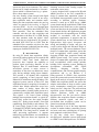
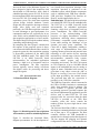
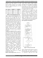
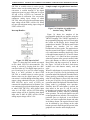
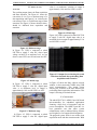
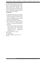
DEVELOPMENT OF USER FRIENDLY DATA ACQUISITION
AND ACTUATION SYSTEM ON EMBEDDED PLATFORM
1
Moolya Ashwar Shankar, 2Mr. Sukesh Rao M.
PG Scholar ,2Assistant Professor, NMAMIT Nitte
Email:[email protected], [email protected]
1
Abstract— Data acquisition is the process
of acquiring signals that measure real
world physical conditions and converting the
resulting samples into digital numeric values
that can be manipulated by a computer.
Data acquisition systems typically convert
analog signals into digital values for
processing. The components of data
acquisition systems include Sample and
Hold circuit or equivalent Signal Sampler
and ADC will convert conditioned sensor
signals to digital values. The proposed
system accepts both digital and analog
signals of different precision. The system
works in t w o ways, data acquisition mode
and actuation mode. During data acquisition
operation the analog values / digital bits are
read b y the processor, where t h e
processing is carried out based on the
constraints provided by the user through
GUI.
The processed data is transferred to the
embedded controller through Host PC with
the help of a USB hub/Host controller,
connected through a serial Bus (USB2.0).
Data acquisition starts with the input
provided by the user command. The
Embedded Host controller unit performs the
data acquisition and transmits to the Host
PC via USB. In data actuation operation the
input can be analog value or digital value.
When user provides digital value in Host PC,
those digital input values are given to
professor via USB. The processor unit
performs processing by converting digital
input to digital output values, result will be
obtained from output port of processor.
When user gives analog values in Host PC,
conversion of analog to discrete values will be
done. Converted discrete values are given as
input to processor unit via USB. The
processing will be performed in processor by
converting input discrete values to analog
output value. Output values will be obtained
from output ports of processor.
Index Terms— GUI, Host PC, mbed NXP
LPC 1768 embedded controller, ADC, DAC,
USB.
I. INTRODUCTION
Data acquisition is the process of sampling
signals that measure real world physical
conditions and converting the resulting samples
into digital numeric values that can be
manipulated by a computer. Data acquisition
systems typically convert analog waveforms
into digital values for processing. Data
acquisition interfaces helps in measuring
information provided by both digital and
analog signals. Digital signals can come from
variety of sources such as switch closures, relay
contacts or TTL compatible interfaces.
Through proper interfaces they can be read
Directly and processed by computers. Similarly
an actuator is a type of driver circuit that is
responsible for controlling a system. An
actuator is the mechanism by which a control
ISSN (PRINT): 2393-8374, (ONLINE): 2394-0697,VOLUME-2, ISSUE-3,2015
17
INTERNATIONAL JOURNAL OF CURRENT ENGINEERING AND SCIENTIFIC RESEARCH (IJCESR)
system acts upon an environment. The control
system can be simple mechanical or electronic
system which is software-based (e.g. a printer
driver, robot control system).
Our user friendly system accepts both digital
and analog signals and it works in two ways,
data acquisition mode and actuation mode.
During the data acquisition mode, the a n al o g
values are passed to the Analog to Digital
converter (ADC) by the user through input
port which is connected to mbed NXP LPC1768
Host controller. Then the embedded Host
controller unit does the data acquisition and
transmits data to the Host PC via USB. During
the data actuation mode the digital values
entered by the user in the host PC are passed to
the mbed NXP LPC1768 via USB. Then the
embedded Host controller unit does the data
actuation and output is obtained from the analog
output port of mbed NXP LPC1768.
II. RELATED WORK
By using PC based data acquisition (DAQ)
systems [1], analog signals can be acquired and
processed. Today Intel based multi-core
processors have acquired the capability to
perform signal processing functions on the
digitized data of multi-channel underwater
surveillance systems. A major concern is
acquisition of data from an underwater sensor
array having multiple analog input channels.
This presents a 96 channel data acquisition
system comprising of Intel processor based
industrial PC mainframe running Windows. The
suggested system consists of three PCI data
acquisition boards for acquiring 96 channels of
acoustic data. Mostly underwater arrays have
more number of analog inputs than the
maximum number of analog inputs present on a
commercially available data acquisition board.
This requires a PC based system utilizing
multiple data acquisition boards. A typical PC
based DAQ system has four major modules
namely PC, Analog input module, Front End
conditioning, DAQ board(s) and software. The
PC based DAQ system in this comprises of
32-channel PCI-24DSI32 analog input boards by
ACQUITEK. This DAQ board is suitable for
audio processing applications. It supports
multi-board synchronization and simultaneous
sampling. These two factors are important for
obtaining accurate beam forming outputs for
underwater sensor arrays.
A newly designed idea is proposed in [2] with
ARM9 processor as the core components to
design a common data acquisition system. A
user-defined data acquisition system is formed
according to different signals. Hardware
structure is made up of Web Server, ARM9
system board and the multi-block STM8L data
acquisition board. With Linux as the operating
system and based on the Qt platform ARM9 as
system board develops the application program
and completes the corresponding tests. It mainly
includes in accordance with the actual
application requirements, It proposes that the
system should focus on the characteristics of
high-precision, high speed, low-power and
strong anti-jamming to design, and gives the
overall system design and structural design of
intelligent nodes. The concrete hardware circuit
design of common data acquisition system has
been accomplished, which mainly includes
designing STM8L data acquisition board and
ARM9 system board]. The concrete software
design of common data acquisition system has
been accomplished, which mainly includes
building Linux operating system, building Qt
development environment, ADC, digital
filtering,
designing
real-time
data
communications, and real-time graphics display
applications and so on. Because it is
battery-powered in STM8L data acquisition
board, the system needs to work with low power.
Based on the analysis of energy consumption in
STM8L data acquisition board, the system has
adaptive mechanisms of sleep to reduce system
power consumption, ensuring the system can
orderly run for a long time. The universal data
acquisition system consisting of hardware and
software platforms, based on ARM9
microprocessor core. We just need to choose
different data acquisition boards according to
different measured signals, and then a
user-defined data acquisition system can be
formed conveniently and flexibly.
Data acquisition is one of the most important
sections in modem industry controlling system,
and more and more technologists are putting
much emphasis on this kind of study.
In [3], they firstly have designed a
microprocessor minimum system which based
on ARM7 kernel Microprocessor S3C44BOX.
ISSN (PRINT): 2393-8374, (ONLINE): 2394-0697,VOLUME-2, ISSUE-3,2015
18
INTERNATIONAL JOURNAL OF CURRENT ENGINEERING AND SCIENTIFIC RESEARCH (IJCESR)
And on the basis of the Minimum System, we
have designed a kind of data acquisition card
which based on USB interface. And a kind of
embedded operating system Jl C/OS- II also has
been transplanted in the data acquisition; we also
have used Jl C/OS- II to manage the whole data
acquisition system. The whole data acquisition
systems design includes hardware circuits'
design and data acquisition interrupt software's
design. After being used and examined
practically, the USB data acquisition card takes
on such advantages as good performance, low
consumption and low cost, especially for its use
value. And it can be embedded in many kinds of
data acquisition applications as a basic module.
This kind of design will help the modem industry
controlling and producing greatly.
By comparing the above papers, conclude that
the response of the proposed system is faster,
convenient and reliable than the above model. In
proposed system, the data acquisition operation
is successfully performed on the mbed NXP
LPC1768 embedded model. This mbed NXP
LPC1768 is an ARM Cortex-M3 based
microcontrollers for embedded applications
featuring a high level of integration and low
power consumption. The data acquisition
systems typically convert analog waveforms
into digital values for processing and hence
sample the signals.
III. SYSTEM DESCRIPTION
3.1 Functional Block Diagram:
Figure 3.1: Block diagram of data acquisition
and actuation system on embedded platform
Figure 3.1 describes the functional Block
diagram representation for the development of
user friendly data acquisition technique. Data
acquisition operation is performed on the
embedded system, which includes components
such as embedded unit, USB Host controller,
USB serial bus, Graphical User Interface on
Host PC and the output display device.
Embedded unit: This data acquisition technique
uses mbed NXP LPC1768 as the embedded unit.
The LPC1768 is an ARM Cortex-M3 based
microcontroller for embedded applications
featuring a high level of integration and low
power consumption. The ARM Cortex-M3
processor is the industry-leading 32-bit
processor for highly deterministic real-time
applications, delivering robust computational
performance, exceptional system response to
events while meeting the challenges of low
dynamic and static power constraints. The
Cortex-M3 is highly configurable, enabling a
wide range of implementations from those
requiring memory protection and powerful trace
technology to cost sensitive devices requiring
minimal area. A broad range of devices include
microcontrollers, automotive body systems,
industrial control systems and wireless
networking and sensors. The LPC1768 operate
at CPU frequencies of up to 100 MHz and the
inputs to the embedded unit may be analog or
digital in nature. Embedded unit converts the
given data it may either convert the ADC or
Digital to Analog Converter (DAC) based
on the input provided by the external sources.
The processed data after the conversion is
provided to the USB Host controller.
The USB Host Controller, which is integrated in
the USB or FireWire hardware to communicate
with a host controller driver in software. The
driver software is typically provided with
an operating system of a personal computer, but
may also be implemented by application-specific
devices such as mbed LPC1768. The data
processed after the conversion from the mbed
LPC1768 is provided to the USB Host
controller, where this device controls the
number of Hosts. It passes single data at a time
to the USB.
The Universal Serial Bus (USB) is a 4-wire bus
that supports communication between a Host and
one or more (up to 127) peripherals. The Host
controller allocates the USB bandwidth to
attached devices through a token-based protocol.
The bus supports hot plugging and dynamic
configuration of the devices. All transactions are
ISSN (PRINT): 2393-8374, (ONLINE): 2394-0697,VOLUME-2, ISSUE-3,2015
19
INTERNATIONAL JOURNAL OF CURRENT ENGINEERING AND SCIENTIFIC RESEARCH (IJCESR)
initiated by the Host controller. The USB
interface includes a Host device is an on-chip
device and Host functions. The switching
protocol is supported through the use of an
external controller.
Table 3.1: Pin configuration for USB
Table 3.1 shows the Pin configuration for the
USB 2.0 serial bus. It uses 4 shielded wires, two
for power (+5v & GND) and two for
differential data signals (labeled as D+ and Din pin out). NRZI (Non Return to Zero Invert)
encoding scheme used to send data with a field
to synchronize the Host and receiver clocks. In
USB data cable Data+ and Data- signals are
transmitted on a twisted pair. Half-duplex
differential signaling helps to combat the effects
of electromagnetic noise on longer lines.
Contrary to popular belief, D+ and D- operate
together; they are not separate simplex
connections. USB provides for a maximum
cable length of 5 meters for devices running at
Hi Speed.
Graphical User Interface (GUI): A graphical
user interface (GUI) is a type of interface that
allows users to interact with mbed controller
through graphical icons and visual indicators
that enable a user to perform interactive tasks.
The user of the GUI does not have to create a
script or type commands at the command line to
accomplish the tasks. Unlike coding programs
to accomplish tasks, the user of a GUI need not
understand the details of how the tasks are
performed. GUI components can include
menus, toolbars, push buttons, radio buttons,
list boxes, and sliders. The actions in a GUI are
usually
performed
through direct
manipulation of the graphical elements. In
addition to computers, GUIs can be found
in hand-held devices such as MP3 players,
portable media players, gaming devices and
smaller household, office and industry
equipment. The creation of GUI is
accomplished with the help of a coding
language called VB.NET.
Host PC and the display device: Host PC is
system which operates through windows
operating system and supports many languages
like Vb.net, C, C++ etc; Host PC is connected to
the processor via USB. In data acquisition
mode, the Host PC is used to verify output result
and in data actuation mode Host PC is used to
provide input to processor via USB.
A display device is an output device that
visually conveys text, graphics and video
information. Information shown on a display
device is called soft copy because the
information exists electronically and is
displayed for a temporary period of time. When
the input information is supplied as an electrical
signal, the display is called an electronic
display. The display device is used for the
visualization of the results. The required output
results are displayed on this display device.
Data acquisition and actuation:
Figure 3.2: Flow chart for ADC
Figure 3.2 shows the ADC module was tested on
mbed LPC1768. The testing is carried by
providing analog input voltage ranging from 0 to
3.3v provided to input port 20 of mbed
ISSN (PRINT): 2393-8374, (ONLINE): 2394-0697,VOLUME-2, ISSUE-3,2015
20
INTERNATIONAL JOURNAL OF CURRENT ENGINEERING AND SCIENTIFIC RESEARCH (IJCESR)
LPC1768. A variable resistor is used to get the
distinct values on the analog input port. ADC
conversion is verified through 12 bit digital
output ports (port 9 to port 14 and port 21 to port
26) and a series of LED’s are connected for
simplification of verification. User can provide
continuous analog input voltage to mbed
LPC1768, when user provides maximum analog
input voltage all the LED’s will be ON. When
user provides minimum analog input voltage all
LED’s will be OFF.
Interrupt Handler:
Figure 3.3: Flow chart for DAC
Figure 3.3 shows the DAC module was tested
on the mbed LPC1768 microcontroller. The
testing is carried by looping back the ADC
converted value as 12 bit digital input (port 9 to
port 14 and port 21 to port 26) values ranging
from 0 to 4095 provided to mbed NXP
LPC1768. A variable resistor is used to get the
distinct values on the digital input port. DAC
conversion is verified through measuring analog
output voltage obtained from port 18 of mbed
NXP LPC1768, and a series of LED’s are
connected for simplification of verification. User
can continuously provide the digital input values
to mbed NXP LPC1768, when digital input
value is 0 all LED’s will be OFF and analog
output voltage will be 0. Similarly when digital
input value is 4095 all LED’s will be ON and
analog output voltage will be 2.54v.
Sample example on graphical user interface:
Figure 3.4: Snapshot of graphical user
interface using VB.NET
Figure 3.4 shows the snapshot of the
programmable graphical user interface using the
VB.NET language. The VB.NET application is
the programming language and is used to display
the results on the display device through the
graphical user interface. The display mode on the
graphical user interface can be either
hexadecimal or binary mode. The graphical user
interface created in the Figure 3.4 mainly consists
of six radio buttons and three check boxes. Three
of the radio buttons namely P1, P2 and P3 shown
in the Figure 3.4 is linked to three operations,
where the response of the system is needed. Other
three radio buttons are linked to operations on
Read, Write and Stop respectively as shown in
the Figure 3.4 Each of the three check boxes
includes two radio buttons namely read and
write.
When P1 radio button is pressed, the data stored
in the port P1 will be read by performing read
operation and will be displayed in hexadecimal or
binary mode by performing write operation. And
when P2 radio button is pressed, the data stored
in the port P2 will be read by performing read
operation and will be displayed in hexadecimal or
binary mode by performing write operation.
Similarly when P3 radio button is pressed, the
data stored in the port P3 will be read by
performing read operation and will be displayed
in hexadecimal or binary mode by performing
write operation. The stop radio button resets the
created graphical user interface. The results for a
particular port are displayed in two different
forms, one in the hexadecimal format and other
in the binary format. The required form of result
can be obtained by just clicking on the radio
buttons present in the dialogue box present in the
graphical user interface under display mode.
ISSN (PRINT): 2393-8374, (ONLINE): 2394-0697,VOLUME-2, ISSUE-3,2015
21
INTERNATIONAL JOURNAL OF CURRENT ENGINEERING AND SCIENTIFIC RESEARCH (IJCESR)
IV. RESULTS AND
ANALYSIS
value is at continuous variation so output is
approximately 1.06v and few LED’s are ON.
The resulting output shows the Data acquisition
and Data actuation. The Figure 4.1 shows the
conversion of A to D, at a moderate stage of a
data acquisition and Figure 4.2 to 4.4 shows the
conversion of D to A, at a different stage of data
actuation. The Figure 4.5 shows decimal values,
should be indicated data acquisition and
actuation.
Figure 4.4: Final stage
Figure 4.4, USB is connected to mbed LPC1768
to supply 5 volts DC, digital input value is at
maximum level so output is approximately 2.54v
and all LED’s are ON.
Figure 4.1: Moderate stage
In Figure 4.1, USB is connected to mbed
LPC1768 to supply 5 volts DC, where input
voltage variation is at moderate level, we can
observe some LED’s are ON and some are OFF.
Figure 4.5: Output Screen showing the result
of the data obtained after performing Data
Acquisition and Actuation
Figure 4.2: Initial stage
In Figure 4.2, USB is connected to mbed
LPC1768 to supply 5 volts DC, digital input
value is at minimum level so output is
approximately 0.02v and all LED’s are OFF.
Figure 4.3: Moderate stage
In Figure 4.3, USB is connected to mbed
LPC1768 to supply 5 volts DC, digital input
In Figure 4.5 shows the Putty software console
window, in that connected COM28 using USB
serial communication. This output screen
showing the resultant of the data obtained for
performing Data Acquisition and actuation. This
output is showing in decimal format.
V. CONCLUSION
The mbed LPC1768 is ARM Cortex-M3 based
microcontrollers for embedded applications
featuring a high level of integration and low
power consumption. The ARM Cortex-M3 is a
next generation core that offers system
enhancements such as enhanced debug features
and a higher level of support block integration.
The proposed system works in two modes, data
acquisition mode and data actuation mode. With
ISSN (PRINT): 2393-8374, (ONLINE): 2394-0697,VOLUME-2, ISSUE-3,2015
22
INTERNATIONAL JOURNAL OF CURRENT ENGINEERING AND SCIENTIFIC RESEARCH (IJCESR)
help of mbed online compiler .bin file is deployed
into mbed LPC1768 through USB for both
modes. In data acquisition mode testing of ADC
module is achieved by mbed LPC1768. Result is
verified through LED’s. Similarly in data
actuation mode loop back of tested ADC module
is used as input to DAC of mbed LPC1768 and
result is verified through analog output port and
shows the result in console window.
REFERENCES
[1] Umar Hamid, Rahim Ali Qamar, Mohsin
Shahzad,”2013,” PC Based Data Acquisition
and Signal Processing for Underwater Sensor
Arrays”; Proceedings of 2013 10th
International Bhurban Conference on Applied
Sciences & Technology(IBCAST).
[2] Wang Jiannong, Wang Wei, ICEMI‟2011,”
The Common Data Acquisition System
Based On Arm9”;The Tenth International
Conference on Electronic Measurement &
Instruments.
[3] Yujun Bao, Xiaoyan Jiang, ICCASM
“2010,” Design of USB Data Acquisition
Card which based upon ARM kernel
Microprocessor”;2010
International
conference on computer Application and
System modeling.
[4] LPC1768 User Manual” Philips
Semiconductors.
[5] www.mbed.org
[6] http://en.wikipedia.org/wiki/Universal
serial bus.
ISSN (PRINT): 2393-8374, (ONLINE): 2394-0697,VOLUME-2, ISSUE-3,2015
23