1
Creating
AXI-LITE
‘Custom IP’
in Vivado
Lab for COMP4601
Developed by: Shivam Garg,
Alexander Kroh
Contents
1
Introduction .................................................................................................................................... 2
2
High-level design configuration ...................................................................................................... 3
3
Creating Custom IP.......................................................................................................................... 4
4
3.a
Generating a Custom IP component ....................................................................................... 4
3.b
Creating a Project file for the Custom IP................................................................................. 7
Customising the Custom IP ........................................................................................................... 10
4.a
AXI Tutorial............................................................................................................................ 10
4.a.i
AXI Writes.......................................................................................................................... 11
4.a.ii
AXI Reads........................................................................................................................... 12
4.b
4.b.i
Customising the Custom IP ................................................................................................... 13
Changes to Slave_AXI ........................................................................................................ 14
4.b.ii Changes to Toplevel .......................................................................................................... 15
5
6
7
Packaging and testing your IP ....................................................................................................... 17
5.a
IP Packager (Within the Custom IP’s Vivado project) ........................................................... 17
5.b
IP upgrade in high-level design (Within the high-level Vivado project) ............................... 20
5.c
Interfacing with the Custom IP ............................................................................................. 21
Implementation Exercises ............................................................................................................. 23
6.a
Timer implementation .......................................................................................................... 23
6.b
FIFO implementation ............................................................................................................ 24
6.c
GPIO implementation ........................................................................................................... 26
6.d
Block RAM implementation .................................................................................................. 27
Conclusion ..................................................................................................................................... 29
1
1 Introduction
The aim of this lab is to introduce a design flow that will allow you to create your own Custom
Intellectual Property (Custom IP) targeted at a Zynq device using Xilinx’s Vivado 2013.4. The lab has
been created for senior undergraduates using the ZedBoard. We assume the reader is familiar with
the use of VHDL for specifying hardware. The lab explains how to modify the generated component,
by focusing on how the AXI-LITE protocol works and how it can be utilised to establish a two-way
data flow between the Processing System (PS) and the hardware component implemented in
programmable logic (PL). This lab concludes on methods for maintaining and integrating this IP as
part of a larger design.
As a high-level overview, this document will cover the following:
Section 2:
Section 3:
Section 4:
Section 5:
Section 6:
Section 7:
Setting up your Vivado high-level design, focussing on the configuration of the
Processing System.
Using Vivado’s built-in tools to generate your own ‘Custom IP’ and modifying this IP.
Provides a tutorial on the AXI protocol that explains the critical modifications that
allow the Slave AXI implementation to be abstracted, thereby making the AXI
communication logic as simple as possible.
Shows you how to package and upgrade your IP. Sample software will be presented
in order to test the modifications that were made to your hardware.
The penultimate section of this documentation consists of a series of
implementation exercises. These exercises are designed to get you comfortable with
developing custom IP, and to familiarise you with alternative ways of interfacing via
the AXI bus.
Concludes this lab by listing methods of going forward and developing your own
hardware based solutions.
By the end of this lab you should be able to generate your own IP quickly, implement hardware
solutions, and effectively utilise the AXI bus to transfer data between the PS and the PL. You’ll also
become proficient in the hardware design flow within the Vivado framework, and learn methods of
debugging for producing hardware solutions as effortlessly as possible.
Assumed knowledge/precursors for this tutorial include:
VHDL coding ability
Read through “Zedboard Getting Started Guide”
Completed the Advanced Embedded Design courses to familiarise yourself with Vivado
(minimum lab 1 and 2)
2
2 High-level design configuration
The first step in this lab is to use Vivado to configure a high-level design that features a ZynQ7
processing core. For detailed instructions on the Vivado design flow please refer to Lab1 of the Xilinx
Advanced Embedded Design course. As we progress through this lab, we will create custom AXI
based IP components that provide fundamental hardware implementations such as a timer, a FIFO
and GPIO.
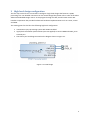
The starting point for this lab is the following high-level configuration:
Instantiate a Zynq7 processing system with UART1 enabled.
Apply block automation (without board pre-sets applied) to connect DDR and FIXED_IO to
external pins
Check that your bock diagram matches the diagram shown in Figure 2-1.
Figure 2-1: Initial design
3
3 Creating Custom IP
In this section you will be creating your own Custom IP which features an AXI-LITE interface for
communication between the Processing System (PS) and the Programmable Logic (PL). We will then
connect this IP to the PS and prepare a project file so that you can readily modify the design later.
3.a Generating a Custom IP component
3.1. Open the project created in Section 2. Click on Project Settings, then ensure that the Target
Language is set to VHDL (else the generated IP will be in Verilog). Click OK when done.
Figure 3-1: Step 3.1, Project target language
3.2. Go to the tools menu > “Create and Package IP”
3.3. On the introductory screen, select the next option.
3.4. Select “Create new AXI4 peripheral” and then in the IP location, go up one level in the directory
hierarchy from where the high-level project file is located. The high-level project directory and
the IP that will be created should be located in the same directory (e.g. C:/…./XX/high-level &
C:/…/XX/IP)
Figure 3-2: Step 3.4, selecting IP type and location
4
3.5. Name the IP as “lab0_ip”, update the display name, and provide a description of the peripheral.
Figure 3-3: Step 3.5, naming the new IP
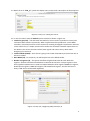
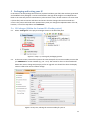
3.6. In the next menu, keep the default options selected as shown in Figure 3-4.
Interface Type (LITE) – Full and Steam AXI allows for burst transfers (4 packets at a time) and
continuous data transfers respectively. When coupled with other peripherals, such as DMA
controllers, these AXI protocols can be essential for meeting throughput requirements. AXI LITE,
on the other hand, is a simpler protocol that satisfies the minimum hardware requirements of
the AXI bus. This means that there will be fewer signals and state to worry about when
designing your custom IP.
Interface Mode (SLAVE) – Since this IP is going to be issued commands by the processor this IP
will act as a Slave.
Data Width (32) – For simplicity, we will keep the bus at the default width.
Number of registers (4) – This option will affect the generated Slave AXI code. With four
registers, the data transferred from Master to Slave will be stored in 4 unique registers. The 4
least significant address bits are used to multiplex between these registers (b0000 first register,
b0100 second register, b1000 third register and b1100 fourth register. The last two bits are
always “b00” due to 32 bit width alignment).
Figure 3-4: Step 3.6, configuring AXI protocol for IP
5
3.7. When you are happy with the configuration, click Next.
3.8. On the “Generation Options” screen, leave the options unchecked and click next.
3.9. Finally, select “Add IP to catalog” and hit finish.
Figure 3-5: Step 3.9, Finishing off the creation of Custom IP
You have now generated your own Custom IP component! In the next section, we will create a
Vivado project file for the Custom IP so that we can independently modify the Custom IP, abstracting
it from the high-level design (Vivado block diagram).
6
3.b Creating a Project file for the Custom IP
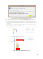
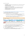
3.10. In the block diagram view (with only the ZynQ7 IP instantiated), select “Add IP” and find the
lab0_ip that you just created.
3.11. Select the “Run connection automation” to the s00_AXI of the Custom IP that we just
created. The end result should resemble that shown in Figure 3-6.
Figure 3-6: Step 3.11, Adding Custom IP to your high level design
3.12.
3.13.
Save the block design and project file.
Right click the lab0_ip_v1_0 (Custom IP) in your design and select “Edit in IP Packager”
Figure 3-7: Step 3.13, opening the IP packager
3.14.
Select “Ok” in the project location screen
7
Figure 3-8: Step 3.14, selecting the project name and location
3.15. When the new instance of Vivado shows up, the first thing to do is close it so that a
permanent project file will form. This will make it easier to edit the IP in future, without the
need to generate (and regenerate) temporary project files, also protecting against data loss if
Vivado crashes.
You should now have two project files as shown in Figure 3-9. One is the high-level module
(lab0) and the second contains the IP (lab0_ip_1.0).
Figure 3-9: Step 3.15, Expected directory structure
8
3.16. Now we will reopen the Vivado project file for the Custom IP. Navigate to the lab0_ip_1.0/
lab0_ip_v1_0_project folder and open the .xpr file shown above.
3.17. Open the VHDL file named “lab0_ip_v_1_0_S00_AXI.vhd”, from the project manager view.
Figure 3-10: Step 3.17, Opening the Slave AXI file
Now that we have a suitable development environment now in place, we can begin to develop our
AXI peripheral. In the following sections of this manual, we will extend the operation of our new IP
and repackage it so that we can upgrade the instantiated component in the high-level module.
9
4 Customising the Custom IP
This section provides an AXI-LITE interface tutorial and will walk you through customising the Slave
AXI file that was generated in Section 3. You will modify the Custom IP component to set the stage
for extending the generated skeleton implementation.
4.a AXI Tutorial
The Advanced eXtensible Interface (AXI) bus protocol was developed by ARM to control access to a
shared bus. Some of the key features of this protocol are as follows:
Independent address, control and data lines
Simple handshaking due to the independent control lines
Burst mode transfer support with the provision of only a starting address
Uses a Master Slave model, with the Master being solely responsible for the arbitration of
the bus; directing writes and requesting reads from the Slave
This section is limited to an overview of the AXI protocol. For more information, see the “AXI
Reference Guide” [2].
The Master accesses a connected Slave by first applying an appropriate address on the address bus.
Each Slave then determines if the provided address lies within its assigned addressable range before
either ignoring or acting on the request. When connection automation was run on your Custom AXI
IP, Vivado inserted a Xilinx AXI Interconnect between the Master and your Slave IP (See the “Xilinx
AXI Interconnect documentation” [3]). The Interconnect provides a layer of abstraction that prevents
a Slave from receiving any signal, unless the significant bits of the address match the assigned
address range of the Slave. This is achieved by multiplexers and internally embedded routing data
and explains why the observable address width of your Slave IP may not match the width of the bus.
The downside of this abstraction layer is the introduction of some delay (which will be seen in the
timing diagrams in the following subsections).
10
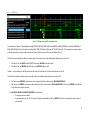
4.a.i
AXI Writes
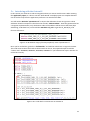
Figure 4-1: Debug output for AXI write transactions
The waveforms in Figure 4-1 show the Master writing 0xFFFFFFFF @ BASE_ADDR (0x0) then 0x00000001 @ BASE_ADDR (0x0), and finally 0x0000000a @
BASE_ADDR+4 (0x4). Note that the signals are prefixed with “M00_AXI” (Master AXI) instead of “S00_AXI” (Slave AXI). This is because the net was assigned
a label by arbitrarily choosing the name of just one of the ports that it connects (in this case, the Master AXI port).
The AXI writes are initiated by the Master as follows, where the numbers refer to the labelled signals between clock cycles 10-12:
1. The Master* sets up WDATA (with 0xFFFFFFFF) and asserts WVALID (write data is valid)
2. The Master* sets up AWADDR (with 0x0) and asserts AWVALID (address valid)
*Master – strictly speaking it is the AXI interconnect which acts as the Master for this Slave AXI component, not the PS.
The Slave then responds as follows, where the numbers refer to the labelled signals between clock cycles 13-15:
3. The Slave asserts AWREADY (write address can be accepted by the Slave, determined by WVALID && AWVALID)
4. The Slave asserts WREADY (write data can be accepted by the Slave, determined by WVALID && AWVALID), at this point, AWADDR is also latched
to free the bus for another operation.
Once WVALID & AWVALID & AWREADY & WREADY are all asserted
o Slave register write is enabled
o On the next clock cycle, the 14th clock cycle in the figure marked with a yellow line, WDATA is written to the appropriate Slave register in
your custom IP.
11
4.a.ii
AXI Reads
Figure 4-2: Debug output for AXI read transactions
The waveforms in Figure 4-2 show the processor reads, via AXI-LITE, from a FIFO at address BASEADDR+4 (0x4). The FIFO contains the data {0x0a, 0x0b,
0x0c, …..}.
The Master initiates an AXI read as follows, where numbers refer to the labelled signals between the clock cycles 175 – 177:
1. For AXI-LITE, the Master generally always has the signal RREADY asserted, signalling that it is able to receive data from the Slave
2. The Master then places the requested address (0x4) onto the ARADDR bus and asserts ARVALID
The Slave then performs the following, where numbers refer to the labelled signals between the clock cycles 177 – 180:
3. The Slave asserts ARREADY to signal that the address has been accepted by the Slave
4. The Slave then sets RDATA to reflect the appropriate data (0x0000000a), and asserts RVALID and de-asserts ARREADY. At this point (the 178th clock
cycle) the correct data has been placed onto the bus and the Master has just one clock cycle to read it before RVALID is de-asserted.
Since the Master (AXI Interconnect) and the Slave are clocked at the same rate (FCLK_CLK0) the RVALID signal can be viewed as a latch signal for the
AXI Interconnect to store this data into its own internal register and later forward it to the up-stream Master, the Zynq Processor.
12
4.b Customising the Custom IP
Based on the tutorial on the AXI protocol in the previous subsection, it should be clear that AXI
signals can be used by the hardware designer to determine whether or not a read or write has been
requested by the Master.
There are a few files and naming conventions to take note of before we begin to modify the IP:
Slave_AXI (lab0_ip_v1_0_S00_AXI.vhd) – a generated file which implements the AXI-LITE
handshaking process and stores all writes to local registers. These same registers are
currently configured to also be used for read values.
Toplevel (lab0_ip_v1_0.vhd) - refers to the VHDL file that encapsulates the Slave_AXI file
described above. You’ll notice that it is largely empty. This is where we will be focussing our
implementation efforts. When coding your own designs, it is recommended that you use this
file only as a connection point between your VHDL components. Given that this is a
relatively short lab, we will code entirely within this file for convenience.
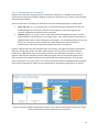
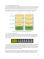
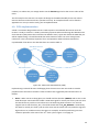
Figure 4-3 below shows the overall organization of our design. The high-level project encapsulates
the Zynq, the AXI Interconnect and your Custom IP block. The source for your custom IP block
resides in an independent project and contains the files mentioned above. The green arrows in
Figure 4-3 denotes the changes we will be making to expose some of the internal signals of the
Slave_AXI file into the Toplevel where we can then design the peripheral directly, or instantiate
other components. The reason for this is so that we preserve the protocol implemented by the Slave
AXI file and concentrate our efforts on the implementation of the device logic (shown in orange).
High Level Design
Lab0_ip (Toplevel)
Zynq7
AXI BUS
AXI
Interconnect
AXI BUS
Data_in
Slave
AXI
Data_out
Latched_addr
Processing
System
Programmable
Logic
Implementation
code
Select signals
Figure 4-3: System diagram denoting the changes we are about to make (green arrows) and a high
level overview of how all the components are connected.
13
4.b.i Changes to Slave_AXI
Figure 4-4 presents a subset of the Slave_AXI design file. You should note that the RDATA bus for AXI
reads is driven by reg_data_out. The generated Slave implementation drives this signal from the
local signals named slv_reg. The first modification will be to introduce four externally visible signals
to take the place of these signals during a read operation. We will call these signals datain as shown
in Figure 4-4.
Figure 4-4: Changes to AXI read data within lab0_ip_v1_0_S00_AXI.vhd
Now that we have taken care of the output values, we next need to expose the data that the master
writes to this Slave so that their values can be used by the Toplevel. In this case, instead of modifying
the Slave logic, we simply map the local signals named slv_reg to external signals named dataout.
Recall from the timing figures in Sections 4.a.i and 4.a.ii, that the address bus value is only valid for a
very short amount of time. The axi_awaddr and axi_araddr registers are used in the generated code
as latches to ensure that their values are persistent for the duration of a transaction. These signals
will also need to be made available to the Toplevel. The changes that need to be made are shown in
Figure 4-5.
Figure 4-5: Exposing the written values and latched addresses within lab0_ip_v1_0_S00_AXI.vhd
To ensure that the Toplevel can access the signals introduced above, the port definition of the
Slave_AXI component needs to be modified as shown in Figure 4-6.
14
Figure 4-6: Required signal additions to the Slave_AXI entity declaration
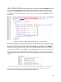
4.b.ii Changes to Toplevel
There are two ways that one can utilise the values from the processor:
The first approach is to use registers which will be accessed independently by both the AXI
bus and the underlying peripheral. The peripheral need not know exactly when a read or
write operation has taken place.
The second approach is to handle AXI communication in real time. One can effectively
‘snoop’ the AXI bus lines and be reactive to communication from the master as it occurs. An
example would be an address which always reads 0, but when written with any value, a
state transition occurs within the peripheral. The data in either case, has no tangible value.
We’ll come back to these ideas in the Section 6, but for now we’ll stick to some simple modifications
so that we can determine if the changes that we have made to the IP source have carried through to
our high-level design.
Your next task is to modify the Toplevel source file to reflect the port changes that were made to the
Slave_AXI component in Section 4.b.i as shown in Figure 4-7. You will also need to declare these
signals within the Toplevel.
Figure 4-7: Signal additions to the port map of the Slave_AXI. Lines 110-129 require no changes.
15
We will now implement some trivial logic (shown in Figure 4-8) for the purposes of testing the
changes that we have made. Notice that the registers which store the data written by the Master
(dataout0, dataout1) are routed to the AXI read registers (datain1, datain0). Writes to register 1
(BASE_ADDR + 0x4) which set the read value of register 0 (BASE_ADDR + 0x0). Similarly, writes to
register 0 set the read value of register 1. Meanwhile, for the reads from register 2 (BASE_ADDR +
0x8) and register 3 (BASE_ADDR + 0xC), the constant values of 3 and 4 will be read respectively and
writes to these registers will be ignored.
Figure 4-8: Simple IP logic to test the changes that we have made
Within the IP project file, check for compilation errors by clicking on the “Synthesise” button in the
left hand pane. Once you have corrected any outstanding errors, all that remains is to save these
changes within the IP. In the next section of this manual, you will update the instantiated
component within your high-level design and test the implementation of your updated IP via the PS.
The importance of the steps outlined in this section is that you no longer have to worry about the
Slave_AXI implementation file because you have exposed all of the signals that will be useful for
your implementation. From now on, you are free to modify only the Toplevel file when changing the
behaviour of your custom IP or to instantiate additional components.
16
5 Packaging and testing your IP
In this Section we will package the Custom IP (Toplevel and Slave_AXI files) that we have generated
and modified. Once packaged, it can be instantiated in the high-level design as an independent IP
block in the same way that we instantiate any other IP block. Then, all that remains is to write some
C (driver-like) code to interact with the IP and ensure that the changes that we have made are
correct. This process will need to be repeated every time you change the implementation of the IP,
however, a lot of the steps below are conditional.
5.a IP Packager (Within the Custom IP’s Vivado project)
5.1.
Select “Package IP” in the project manager section in the left hand pane.
Figure 5-1: Step 5.1, starting the packaging process
5.2.
At the start screen, leave all the options the same except for the version number; ensure that
you INCREASE the version number (e.g. 1.0 -> 2.0). The reason for this is so that Vivado will
detect the version change and prompt you for an upgrade. You should also alter the display
name to reflect the version number change.
Figure 5-2: Step 5.2, altering the version number for your IP
17
5.3.
If the changes to the file involved adding new VHDL files, they must be added in the “IP File
Groups” to both the “VHDL synthesis” and “VHDL Simulation” folders, as shown in Figure 5-3.
Figure 5-3: Step 5.3, Add VHDL files to the IP definition if needed
5.4.
If the ports to the Toplevel have been changed, then use the “IP Ports” page by clicking on the
Port import dialog and following the prompts.
Figure 5-4: Step 5.4, Modifying IP ports if needed
5.5.
If you used the “IP ports” page to add/remove ports, you should now go to the “IP GUI
Customization Layout” and use the IP GUI customization layout wizard to regenerate the
18
image of the IP component. Simply follow the “run the wizard” link to regenerate the diagram
of the IP.
Figure 5-5: Step 5.5, Regenerating the IP GUI
5.6.
Complete the process by clicking on the Re-Package IP button in the “Review and package”
screen.
Figure 5-6: Step 5.6, finalising the packaging process
19
Screens that were skipped:
IP compatibility - is used to list the valid target boards for the IP. It should always include the
ZYNQ board for our designs.
IP Customisation Parameters – should be used if the customisation parameters (generic
parameters) for the IP have been changed.
IP interfaces – This screen is used to match or create a standardised interface port by
grouping signals (e.g. a FIFO_WRITE port for interfacing with a Xilinx FIFO instance).
IP Addressing and Memory – Informational only
IP Licencing and Security – Informational only
5.b IP upgrade in high-level design (Within the high-level Vivado project)
5.7. Reopen the high-level design Vivado file and open the Block Design
5.8. Select the TCL console window and run the following commands
a. ‘update_ip_catalog –rebuild’ This refreshes the IP repositories specified in
Project Settings > IP > IP Repositories (you can do this manually if you wish)
b. ‘report_ip_status -name ip_status_1’ This generates an IP report which
shows whether or not the IP in your design are up to date. You should see that
lab0_ip_0 has a “Major Version Change” as shown in Figure 5-7.
Figure 5-7: Step 5.9, Vivado reporting changes to the IP in your high-level design
5.9.
Tick the checkbox associated with our IP and click the upgrade selected button. Vivado will
now upgrade the instantiated IP while retaining all existing connections.
5.10. Regenerate the HDL wrapper for your high-level design, and save your project file.
5.11. Generate a bitstream for the project.
5.12. Once generated, open the ‘Implemented Design’ and export it to the SDK so that we can
begin the development of driver software for interfacing with our custom IP.
20
5.c Interfacing with the Custom IP
In this section you will write C code to integrate and test our new IP with the CPU. When creating
the application project, it is best to use the “Hello World” example project as a template because
one of the first steps that the application performs is to initialize the UART.
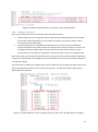
You will need to #include “xparameters.h” to import the definitions shown in Figure 5-8. These
addresses should correspond to those listed in Vivado’s “Address Editor”. Since the generated IP has
a 4 register implementation, only the bottom 4 bits of the address will be seen at the Slave (byte
addressing, 32 bit data bus). You should also #include <xil_io.h> to get the Xil_Out32/Xil_in32
function definitions.
Figure 5-8: AXI address range of the AXI peripheral, inside “xparameters.h”
Once you’ve verified this, go back to “helloworld.c” and add the code shown in Figure 5-9 below.
This code writes 4 values and reads 4 values back from the IP. The expected output should be
“Values read = 00000002, 00000001, 00000003, 00000004” if you followed the steps in Section 4.b
of this lab correctly.
Figure 5-9: C code which is used to test our Custom IP
21
If you were to write to the address: XPAR_LAB0_IP_0_S00_AXI_BASEADDR + 0x10, it would mimic
the effect of writing to XPAR_LAB0_IP_0_S00_AXI_BASEADDR + 0x0, since the Slave only sees the
least significant 4 bits of the address.
The xil_io.h file contains definitions for IO functions of various widths such as Xil_in8, Xil_out16. You
may have considered using these functions given that we are reading and writing such small data
sizes. A problem with this approach lies in our AXI bus abstraction layer where we have chosen not
to expose the signals required for detecting these access widths. It is common to find that AXI
devices will only support 32 bit IO.
You will also find definitions for fixed size data types, such as u32 (unsigned 32 bit), within xil_io.h.
As you may already be aware, the size of an int data type is not well defined. For this reason, it is
good practice to use fixed size data types when accessing fixed size peripheral registers.
22
6 Implementation Exercises
By now, you should be familiar with the process of modifying a Custom IP component, repackaging
the IP and integrating it back into your high-level design. In this section, we will extend the custom IP
design to produce a useful AXI peripheral. The peripheral will be split into 4 functions; a timer, a
FIFO, a GPIO controller and CPU accessible BRAM. All exercises are intended to be implemented in
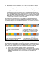
the Toplevel file of the Custom IP. The AXI register layout for this lab is shown in Figure 6-1.
Writes via AXI
Reads via AXI
0xYY0
Start/Stop/Reset timer
Read timer value
0xYY4
Write to FIFO
Pull value from FIFO
0xYY8
Set LED (8) value
Read physical switch (8)
values
0xYYB
0x0 | ADDR
(sets addr for R/W)
0x80000000 | DATA
(commit write)
Read from BRAM at set
address
Address
Figure 6-1: AXI Protocol for the Implementations to follow
6.a Timer implementation
The first task will be to implement a simple AXI accessible, 32 bit timer within the FPGA. The timer
will run at FCLK_CLK0 and counts the number of clock cycles elapsed since the timer was last reset
by the user (CPU; AXI Master). The register interface for the timer is shown in Error! Reference
source not found.:
Bit 31 30 ….. …… ……
1
0
Function on write n/a n/a ….. …… …… Reset Enable
Function on read
Timer value
Table 6-1: Timer register interface
The timer can be considered to be a counter which has a reset signal controlled by bit 1 of dataout0
and an enable counter signal controlled by bit 0 of dataout0. In this case, the counter is counting
rising edges in the FCLK_CLK0 signal (number of FCLK_CLK0 periods elapsed). The implementation of
the timer will be quite simple since AXI writes from the Master to the Slave are stored in the Slave
registers which we have piped out to the Toplevel.
After implementing the timer control logic, all that remains is to get the value of the timer back to
the Master (PS). Since the selected AXI data bus width was 32 bits, we will implement a 32 bit timer.
The timer value will need to be provided every time the user reads from 0xYY0 (where YY is any
23
number). To achieve this, we simply need to set the datain0 signal to be the current value of the
timer.
The final step for this exercise is to export the design to the SDK and modify the IP test code to
exercise the timer and ensure that it operates correctly. An example solution can be found in
Appendix A in case you wish to verify your IP implementation.
6.b FIFO implementation
A FIFO is a common design element that is used to queue a transmitted data stream until the
receiver is ready to collect it. A FIFO is particularly important when transferring data between two
clock domains (subsystems that are clocked at different rates). Figure 6-2 details the FSM that you
will be implementing. It should be noted that state transitions must not occur during an AXI
transaction. This is particularly important for a read operation where the data read will be
unpredictable if the data on the data bus does not remain stable. S.
AXI Write occurs
Insert AXI
WDATA into
FIFO
Idle
Increment FIFO
insertion
pointer
AXI read occurs
Read RDATA
from FIFO
Increment
FIFO read
position
(valid for next
read)
Figure 6-2: FIFO Finite State Machine (FSM)
Implementing a FIFO will be more challenging than the timer since we now need to consider
peripheral state and state transitions. State transitions are triggered by AXI communication as
follows:
Write – When a write is taking place, we should read the data bus (WDATA) and set this as the
FIFO data input. We should also enable a FIFO write signal for exactly one clock cycle such that
the FIFO knows to push the current data to its tail. Referring back to Section 4.a.i and the
original source code for Slave_AXI, it should be noted that the S_AXI_WREADY is asserted by
the Slave for exactly one clock cycle once the write was successful. We can probe this signal as
high and once so, enable a write to the FIFO. For example, we will be performing our FIFO
insertion operation at the start of the 14th clock cycle in Figure 4-1 on page 11.
24
Read – From the timing diagrams in Section 4.a.ii on pages 11 and 12, it should be apparent
that the Slave has only a couple of clock cycles to correctly set the data to be read onto the data
bus. Instead of trying to provide a read result at the exact instance it is required, we shall set up
the next read value as soon as any read transaction has completed. Referring back to Section
4.a.ii on page 12 and the original source code, it should be noted that when S_AXI_RVALID is
asserted, the Slave has updated the data bus with valid read data. Furthermore, this signal is
asserted for exactly 1 clock cycle. If we were to wait for this signal to be asserted on the rising
edge of a clock pulse (which would mean the falling edge of the signal S_AXI_RVALID), we know
that the data, datain1, has been accepted by the Master and we can safely replace the value of
datain1 with the next value in the FIFO. The position in time at which this happens is denoted
by the start of the 179th clock cycle in Figure 4-2 on page 12.
The last point to note is that you also have to check the address of the write/read operation to
ensure that it is a FIFO operation (denoted by the addressing corresponding to 0xYY4). However if
you refer back to the timing diagrams in Figure 4-1 and Figure 4-2, you’ll notice that the read/write
address is only valid for a very small amount of time. Therefore, we will need to make use of the
latched write and read addresses and check that the (3 downto 2) bits are equal to “01”.
1
2
3
Read ptr
0
0
1
0
3
2
Write ptr
3
4
0
0
0
Read ptr
Write ptr
Write ptr
1. Initial FIFO, after 3 values have been
written
7
2
5
2. After 3 values read by user, note that the
next read should not move read ptr. Set bit 31
to indicate that the current read is invalid
6
7
8
9
Read ptr
3. After 4 more values have been written by
the user, note read ptr is now valid
10
11
Read ptr
Write ptr
6
4. More values written, note the write ptr has
moved beyond read ptr. Undefined behaviour.
Figure 6-3: Run through of FIFO behaviour
The FIFO diagrams in Figure 6-3 denote the functioning of the FIFO; they should all be fairly easy to
follow. The one which causes some concern is the 4th diagram where the user has written over data
that has not yet been read by the user. It is up to you to decide how to respond in this case:
a. Just ignore the transaction and assume the user knows not to overfill the FIFO
b. Store the current size of the FIFO by counting writes and decrement with reads. If the FIFO is
full, the request should be ignored. Note that it will not be possible to provide the client with
immediate feedback when this occurs as this information is only reported by a read
transaction.
25
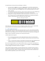
The specification for the FIFO that you will design is as follows:
FIFO data width of 16 bits and a capacity of 1024 words. This should be implemented as
block ram in the Toplevel. The BRAM should have both an address and a data width of 16. If
you need a refresher on the use of BRAM refer to the “Distributed and Block ram on Xilinx
FPGA’s” guide [5]
If we reach the end of FIFO addressing, reads and writes should wrap around the BRAM. This
can trivially be achieved by ignoring underflows and overflows in FIFO position.
Reading from an empty FIFO should not affect the FIFO position. If the user tries to read
from an empty FIFO, bit 31 (Most Significant Bit) should be set to indicate that the data is
invalid. It is expected that the user checks this bit for data validity.
Table 6-2: FIFO register interface
Bit
31
30 …..
Read
Function on read Invalid n/a …..
Function on write
n/a
n/a …..
15
……
1
0
Data out
Data in
At this stage, you should be able to verify your design by writing C code on the PS to sequentially
push 1023 values onto the HW FIFO and then read them back in the same order.
6.c GPIO implementation
The GPIO implementation will mimic that of the Xilinx GPIO IP as seen in the Advanced Embedded
design (AED) Lab 1, however, it will be implemented entirely within our Custom IP component. This
exercise will involve adding ports to our IP as well as external pins and constraints to our high-level
design in order to extend the connectivity of our IP beyond the AXI bus.
We will implement two registers:
LED – The value of this register can be assigned directly from the most recent AXI write
transaction (dataout2). The output of this register should be directly connected to the LED
pins.
Switch – The value of this register is associated with the logical state of the SWITCH pins and
should be reported on the data bus during AXI read transactions from datain2.
Once you have implemented this very simple hardware solution, you will need to repackage the IP.
Since you have added two ports to the IP, you’ll need to run the “IP ports” and “GUI customisation”
of the IP packager as described in Section 5.a on page 17.
Finally, within the high-level design, you need to declare the LED’s and SW’s and connect them to
external pins (see AED lab1 for pin assignments within the xdc file and refer to the “Zedboard user
manual” [4] for the IO pin numbers). A sample constraints file for both the LED’s and Switches has
been provided in Appendix B, if you are stuck at this stage.
26
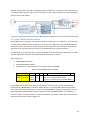
Figure 6-4 shows what your high-level design should resemble. For testing your IP through the PS, it
is recommended that you write an infinite loop that reads the switch values and writes this pattern
back out to the LED register.
Figure 6-4: High-Level Vivado project file, denoting the relevant pin to port connections to be made
6.d Block RAM implementation
Block RAM plays an important role in peripheral local storage for PL IP components. As an example,
you may wish to perform a DSP operation on an image. This image may need to be uploaded from
the CPU into the IP for efficient random data access. The image may also need to be downloaded
again later such that the processed result can be forwarded to the next process block.
For this exercise, it is assumed that you are now familiar with the design flow. We provide you with
only the register API and leave the implementation details entirely to you.
API Assumptions:
16 bit BRAM data width.
16 bit BRAM address width.
The Master can read and write to any address within the BRAM.
Table 6-3: Block RAM register interface
Bit
Function on read
Function on write
31
30 ….. 15
……
0
n/a n/a …..
Data at active address
A/D n/a ….. If bit 31 = 0: Active address select
select
If bit 31 = 1: Data to write to active address
Bit 31 selects the context for an AXI write transaction. If this bit is not set, the data should be
interpreted as a BRAM address selection. When this bit is set, the AXI data represents the 16bit
value which should be written to the current active BRAM address. During a read request, bit 31 is
always ignored and data should always be read from the active BRAM address. For example, to
perform a read or write transaction at a particular address, you would need to write a driver which
executes the functions shown in Figure 6-5.
27
Figure 6-5: C functions to interface with the BRAM within the Custom IP
28
7 Conclusion
Now that you are comfortable with utilising Vivado’s built-in tools to generate and modify Custom
IP, and the design flow related to the process; it’s time to go out and design full-fledged hardware
solutions. While designing your own solutions we have a few recommendations:
Simulation – In terms of compilation time and quality of debugging output, Simulation
provides the fastest way to test your design. You should first make sure that your individual
components are flawless before attempting to integrate them with the AXI bus. This will
save a substantial amount of time when diagnosing faults. One important point to keep in
mind of while when simulating on an FPGA, with clock speeds in the MegaHertz range, is
that the number of clock cycles that occur within a second is more than what you could
possibly view within a simulation frame. Consequently ensure that your FSMs’ within the
custom IP are initiated by an AXI transaction, and STOP when the transaction has completed.
Your FSMs should wait for a second AXI transaction before continuing the data processing.
This is particularly evident if you decide to print characters to the console between reading
and writing data from the Custom IP. A large amount of clock cycles will be used up writing
out to the UART, thus distorting your perception of time elapsed between the two AXI
transactions.
Debug – If your hardware is not working the way you envisioned (despite simulations telling
you otherwise) one method of identifying the problem is to set all relevant signals as
outputs to the Toplevel of the Custom IP. Then, utilising the knowledge gained in lab2 of
Advanced Embedded Design, set all of these ports as debug. Once you have assigned the
debug cores, set the waveform to trigger on a change in one of the AXI signals and run
through your software. Finally, analyse the waveform to work out where the issue lies. This
approach has been tried and found to be much faster at identifying problems than trying to
simulate your Toplevel/Custom IP individually since that approach involves having to
“simulate” Master AXI behaviour!
Advanced users – If you can churn out perfect (syntax error free) VHDL every time then
potentially you may wish to skip the IP synthesis & repackaging every time and instead
modify the files within C:\....\XX\HIGH-LEVEL\HIGH-LEVEL.srcs\sources_1\bd\system\ip\
system_lab0_ip_0_0\hdl\*.vhd. The obvious traps with this method include: a much longer
time for the compilation to fail on syntax errors, and the fact that you can only modify the
logic of the IP and not add extra VHDL files and ports to the definition of the IP. For most
users it is recommended that you repackage and upgrade the IP every time, as the extra
minute or two added via this process allows for faster identification and fix-up of errors &
warnings should they occur.
29
References
[1] Xilinx Custom IP guide, slightly outdated but quite comprehensive guide to Custom IP
http://www.xilinx.com/support/documentation/application_notes/xapp1168-axi-ip-integrator.pdf
[2] AXI reference guide
http://www.xilinx.com/support/documentation/ip_documentation/ug761_axi_reference_guide.pdf
[3] Xillinx AXI Interconnect
http://www.xilinx.com/support/documentation/ip_documentation/axi_interconnect/v2_1/pg059axi-interconnect.pdf
[4] Zedboard user manual
http://www.zedboard.org/sites/default/files/ZedBoard_HW_UG_v1_1.pdf
[5] Block and distributed RAM’s on Xilinx
http://vhdlguru.blogspot.com.au/2011/01/block-and-distributed-rams-on-xilinx.html
30
Appendix
Appendix A (Timer Solution)
--Timer implementation: uses the dataout0 signal to represent
--the current value which has been written to the timer’s control
--register. And datain0 signal to output the timer value.
process(clk,dataout0)
begin
if (dataout0(1) = '1') then
--"asynchronous" reset
timer32 <= (others=>'0');
else
if (rising_edge(clk)) then
if (dataout0(0) = '1') then
timer32 <= timer32 + X"00000001";
end if;
end if;
end if;
end process;
datain0 <= timer32;
31
Appendix B (GPIO constraints)
########################################################
# LED constraints
#
########################################################
set_property IOSTANDARD LVCMOS33 [get_ports {led_out[7]}]
set_property IOSTANDARD LVCMOS33 [get_ports {led_out[6]}]
set_property IOSTANDARD LVCMOS33 [get_ports {led_out[5]}]
set_property IOSTANDARD LVCMOS33 [get_ports {led_out[4]}]
set_property IOSTANDARD LVCMOS33 [get_ports {led_out[3]}]
set_property IOSTANDARD LVCMOS33 [get_ports {led_out[2]}]
set_property IOSTANDARD LVCMOS33 [get_ports {led_out[1]}]
set_property IOSTANDARD LVCMOS33 [get_ports {led_out[0]}]
set_property PACKAGE_PIN U14 [get_ports {led_out[7]}]
set_property PACKAGE_PIN U19 [get_ports {led_out[6]}]
set_property PACKAGE_PIN W22 [get_ports {led_out[5]}]
set_property PACKAGE_PIN V22 [get_ports {led_out[4]}]
set_property PACKAGE_PIN U21 [get_ports {led_out[3]}]
set_property PACKAGE_PIN U22 [get_ports {led_out[2]}]
set_property PACKAGE_PIN T21 [get_ports {led_out[1]}]
set_property PACKAGE_PIN T22 [get_ports {led_out[0]}]
########################################################
# Switch constraints
#
########################################################
set_property IOSTANDARD LVCMOS33 [get_ports {sw_in[7]}]
set_property IOSTANDARD LVCMOS33 [get_ports {sw_in[6]}]
set_property IOSTANDARD LVCMOS33 [get_ports {sw_in[5]}]
set_property IOSTANDARD LVCMOS33 [get_ports {sw_in[4]}]
set_property IOSTANDARD LVCMOS33 [get_ports {sw_in[3]}]
set_property IOSTANDARD LVCMOS33 [get_ports {sw_in[2]}]
set_property IOSTANDARD LVCMOS33 [get_ports {sw_in[1]}]
set_property IOSTANDARD LVCMOS33 [get_ports {sw_in[0]}]
set_property PACKAGE_PIN M15 [get_ports {sw_in[7]}]
set_property PACKAGE_PIN H17 [get_ports {sw_in[6]}]
set_property PACKAGE_PIN H18 [get_ports {sw_in[5]}]
set_property PACKAGE_PIN H19 [get_ports {sw_in[4]}]
set_property PACKAGE_PIN F21 [get_ports {sw_in[3]}]
set_property PACKAGE_PIN H22 [get_ports {sw_in[2]}]
set_property PACKAGE_PIN G22 [get_ports {sw_in[1]}]
set_property PACKAGE_PIN F22 [get_ports {sw_in[0]}]
32