1
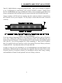
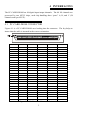
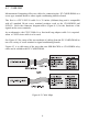
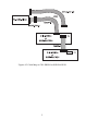
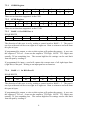
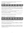
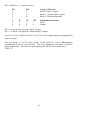
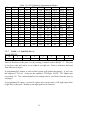
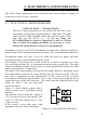
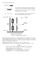
PC-CARD-DIO48
User’s Manual
Revision 5
August, 2001
MEGA-FIFO, the CIO prefix to data acquisition board model numbers, the PCM prefix to data
acquisition board model numbers, PCM-DAS08, PCM-D24C3, PCM-DAC02, PCM-COM422,
PCM-COM485, PCM-DMM, PCM-DAS16D/12, PCM-DAS16S/12, PCM-DAS16D/16,
PCM-DAS16S/16, PCI-DAS6402/16, Universal Library, InstaCal, Harsh Environment
Warranty and Measurement Computing Corporation are registered trademarks of Measurement
Computing Corporation.
IBM, PC, and PC/AT are trademarks of International Business Machines Corp. Windows is a
trademark of Microsoft Corp. All other trademarks are the property of their respective owners.
Information furnished by Measurement Computing Corp. is believed to be accurate and
reliable. However, no responsibility is assumed by Measurement Computing Corporation
neither for its use; nor for any infringements of patents or other rights of third parties, which
may result from its use. No license is granted by implication or otherwise under any patent or
copyrights of Measurement Computing Corporation.
All rights reserved. No part of this publication may be reproduced, stored in a retrieval system,
or transmitted, in any form by any means, electronic, mechanical, by photocopying, recording
or otherwise without the prior written permission of Measurement Computing Corporation.
Notice
Measurement Computing Corporation does not authorize any
Measurement Computing Corporation product for use in life support
systems and/or devices without the written approval of the President of
Measurement Computing Corporation Life support devices/systems are
devices or systems which, a) are intended for surgical implantation into
the body, or b) support or sustain life and whose failure to perform can
be reasonably expected to result in injury. Measurement Computing
Corp. products are not designed with the components required, and are
not subject to the testing required to ensure a level of reliability suitable
for the treatment and diagnosis of people.
(C) Copyright 2001 Measurement Computing Corporation
HM PC-CARD-DIO48.lwp
TABLE OF CONTENTS
1 INTRODUCTION . . . . . . . . . . . . . . . . . . . . . . . .
2 SOFTWARE INSTALLATION . . . . . . . . . . . . . . .
3 HARDWARE INSTALLATION . . . . . . . . . . . . . . .
4 INTERFACING . . . . . . . . . . . . . . . . . . . . . . . . . .
4.1 PC-CARD-DIO48 CONNECTOR . . . . . . . . . . .
4.2 CABLING . . . . . . . . . . . . . . . . . . . . . . . . . .
5 PROGRAMMING & APPLICATIONS . . . . . . . . . .
5.1 PROGRAMMING LANGUAGES . . . . . . . . . . .
5.2 PACKAGED APPLICATIONS PROGRAMS . . .
6 CALIBRATION & SERVICES . . . . . . . . . . . . . . .
7 I/O ADDRESS MAP & REGISTER FUNCTIONS . .
7.1 CONTROL REGISTERS . . . . . . . . . . . . . . . . .
7.2 PORT ADDRESSES & FUNCTIONS . . . . . . . . .
7.2.1 CORR Register . . . . . . . . . . . . . . . . . . . .
7.2.2 CCSR Register . . . . . . . . . . . . . . . . . . . .
7.2.3 BASE + 0 1st DIO Port A . . . . . . . . . . . . .
7.2.4 BASE + 1 1st DIO Port B . . . . . . . . . . . .
7.2.5 BASE + 2 1st DIO Port C . . . . . . . . . . . .
7.2.6 BASE + 3 1st 82C55 Configuration Register
7.2.7 BASE + 4 2nd DIO Port A . . . . . . . . . . . .
7.2.8 BASE + 5 2nd DIO Port B . . . . . . . . . . . .
7.2.9 BASE + 6 2nd DIO Port C . . . . . . . . . . . .
7.2.10 BASE + 7 2nd 82C55 Configuration Register
8 SPECIFICATIONS . . . . . . . . . . . . . . . . . . . . . . .
9 ELECTRONICS AND INTERFACING . . . . . . . . . .
9.1 PULL-UP/PULL-DOWN RESISTORS . . . . . . . .
9.2 TTL TO SOLID STATE RELAYS . . . . . . . . . .
9.3 VOLTAGE DIVIDERS . . . . . . . . . . . . . . . . . .
9.4 LOW PASS FILTERS DE-BOUNCE INPUTS . .
............... 1
............... 1
............... 2
............... 3
............... 3
............... 4
............... 6
............... 6
............... 6
............... 6
............... 7
............... 7
............... 7
............... 8
............... 8
............... 8
............... 8
............... 9
............... 9
. . . . . . . . . . . . . . 11
. . . . . . . . . . . . . . 12
. . . . . . . . . . . . . . 12
. . . . . . . . . . . . . 12
. . . . . . . . . . . . . . 14
. . . . . . . . . . . . . . 15
. . . . . . . . . . . . . . 15
. . . . . . . . . . . . . . 16
. . . . . . . . . . . . . . 16
. . . . . . . . . . . . . . 18
This page is blank.
1 INTRODUCTION
The PC-CARD-DIO48 is a data acquisition and control board for IBM PC compatible
computers having PC-CARD/PCMCIA type slots. The primary functional elements
of the board are a pair 82C55 digital I/O chips. The 82C55 chip uses TTL logic. Each
has 24, digital, bi-directional (input or output) channels (Figure 1-1).
Figure 1-1. PC-CARD-DIO48 Block Diagram
2 SOFTWARE INSTALLATION
InstaCal is the installation, calibration and test software supplied with your data
acquisition / IO hardware. The complete InstaCal package is also included with the
Universal Library. If you have ordered the Universal Library, use the Universal
Library disk set to install InstaCal. The installation will create all required files and
unpack the various pieces of compressed software. To install InstaCal, refer to the
Extended Software Installation Manual for complete instructions.
1
3 HARDWARE INSTALLATION
The PC-CARD-DIO48 is completely plug and play. There are no switches or jumpers
to set. Configuration is controlled by your systems’ PCMCIA software. Simply insert
the PC-CARD-DIO48 into any available slot. Refer to the orientation guide below for
proper orientation of the card (the typical system orients the card with the label up).
Figure 3-1shows a PCM card case looking into the connector which is inserted into
the PCMCIA slot of your computer. The key helps to insure that the board is inserted
correctly.
Figure 3-1. Card Orientation
If you are using an operating system with support for Plug and Play (such as Windows
95 or 98), a dialog box will pop up upon insertion of the card indicating that new
hardware has been detected. If the information file for this board is not already loaded
onto your PC, you will be prompted for a disk containing it. The InstaCal software
that was supplied with your board (as well as the optional Universal Library software)
contains this file. Just insert the disk or CD and click OK.
In order to easily test your installation, it is recommended that you install InstaCal, the
installation, calibration and test utility that was supplied with your board. Refer to the
Extended Software Installation Manual for information on the initial setup, loading,
and installation of InstaCal and optional Universal Library software.
2
4 INTERFACING
The PC-CARD-DIO48 has 48 digital input/output channels. The 48 I/O channels are
processed by two 82C55 chips, each chip handling three “ports” A, B, and C (24
channels total per 82C55).
4.1 PC-CARD-DIO48 CONNECTOR
Figure 4-1 is a PC-CARD-DIO48 case looking into the connector. The key helps to
insure that the cable is inserted in the correct orientation.
50
PIN NO.
1
2
3
4
5
6
7
8
9
10
11
12
13
14
15
16
17
18
19
20
21
22
23
24
25
1
NAME
A7
A6
A5
A4
A3
A2
A1
A0
B7
B6
B5
B4
B3
B2
B1
B0
C7
C6
C5
C4
C3
C2
C1
C0
A7
PORT NO.
2
2
2
2
2
2
2
2
2
2
2
2
2
2
2
2
2
2
2
2
2
2
2
2
1
PIN NO.
26
27
28
29
30
31
32
33
34
35
36
37
38
39
40
41
42
43
44
45
46
47
48
49
50
NAME
A6
A5
A4
A3
A2
A1
A0
B7
B6
B5
B4
B3
B2
B1
B0
C7
C6
C5
C4
C3
C2
C1
C0
+5V
GND
Figure 4-1. I/O Connector Pin-out & Orientation
3
PORT NO.
1
1
1
1
1
1
1
1
1
1
1
1
1
1
1
1
1
1
1
1
1
1
1
-
4.2 CABLING
Measurement Computing offers two cables for connecting the PC-CARD-DIO48 to a
screw-type terminal board or other signal conditioning interface board.
The first is a CPCC-50F-39 cable. It is 39 inches (990mm) long and is compatible
with all standard 50-pin screw terminal products such as the CIO-MINI50 and
SCB-50. Refer the connector diagram above (Figure 4-1) for the functions of the
signals at the screw terminals.
As an alternative, the CPCC-50M-4 is a four-inch long adapter cable. It is required
when a C50FF-series cable is to be used.
See Figure 4-2 for a map of the two methods of cabling from the PC-CARD-DIO48 to
one of a variety of screw terminal or signal conditioning boards.
Figure 4-3 is a cable map of the ways that two SSR-RACK24 or CIO-ERB24 relay
racks can be cabled to the PC-CARD-DIO48.
Figure 4-2. Cable Maps
4
Figure 4-3 Cable Map to CIO-ERB24 or SSR-RACK24
5
5 PROGRAMMING & APPLICATIONS
5.1 PROGRAMMING LANGUAGES
Universal Library provides complete access to the PC-CARD-DIO48 functions from a
range of programming Windows languages. If you are planning to write programs, or
would like to run the example programs for Visual Basic or any other language, please
turn now to the Universal Library manual.
5.2 PACKAGED APPLICATIONS PROGRAMS
Many packaged application programs, such as SoftWIRE™, have drivers for the
PC-CARD-DIO48. If the package you own does not appear to have drivers, please
call us with the package name and the revision number from the install disks. We will
research the package for you and advise you on how to obtain the correct drivers.
6 CALIBRATION & SERVICES
There is no calibration required. The case cannot be opened and there are no parts
inside which you can service. There are no socketted components.
Opening the PC-CARD-DIO48 case will void your warranty!
If you
PC-CARD-DIO48 requires service, please contact the factory for an RMA# and return
it.
6
7 I/O ADDRESS MAP & REGISTER FUNCTIONS
A base address register controls the beginning, or “Base” address of the I/O addresses
occupied by the registers of the PC-CARD-DIO48. Nine addresses are used. The
base address is assigned by PCMCIA software, read by InstaCal and stored in the
CB.CFG file installed in your computer. Please read about installing and using
InstaCal.
7.1 CONTROL REGISTERS
After installation and a base address has been established, the PC-CARD-DIO48 can
be controlled by reading and writing to the registers. While it is possible to write your
own control routines, many have been written and are available in Universal Library
for Windows programming languages.
NOTE ON REGISTER PROGRAMMING SUPPORT
Only limited support for assembly language or direct register programming is
available. Register level programming should only be attempted by experienced
programmers. We support the use of the PC-CARD-DIO48 through high level
languages using Universal Library and the example programs provided.
7.2 PORT ADDRESSES & FUNCTIONS
Table 7-1 lists the card registers and their function. All registers perform 8-bit byte
operations. A Port C can be divided into two, 4-bit ports, CU (upper) and CL (lower).
Table 7-1. Card Register Functions
READ
WRITE
CORREG COR REGISTER
COR REGISTER
CCSRREG CCSR REGISTER
CCSR REGISTER
Base + 0
Digital Input - 1st Port A Data
Digital Output - 1st Port A Data
Base + 1
Digital Input - 1st Port B Data
Digital Output - 1st Port B Data
Base + 2
Digital Input - 1st Port C Data
Digital Output - 1st Port C Data
Base + 3
No readback function
1st 8255 Configuration
Base + 4
Digital Input - 2nd Port A Data
Digital Output - 2nd Port A Data
Base + 5
Digital Input - 2nd Port B Data
Digital Output - 2nd Port B Data
Base + 6
Digital Input - 2nd Port C Data
Digital Output - 2nd Port C Data
Base + 7
No readback function
2nd 8255 Configuration
REGISTER
7
7.2.1
CORR Register
7
x
6
x
5
x
4
x
3
x
2
x
1
x
0
x
3
x
2
x
1
x
0
x
3
A3
2
A2
1
A1
0
A0
There are no functions supported in the COR.
7.2.2
7
x
CCSR Register
6
x
5
x
4
x
There are no functions supported in the CCSR.
7.2.3 BASE + 0 1st DIO Port A
READ/WRITE
7b
6
5
4
A7
A6
A5
A4
The direction of this port is set by writing a control word to BASE + 3. The port is
one byte wide and can be set as eight-in or eight-out. Data is written to and read from
this port in bytes.
If programmed for output, a write to this register will update the outputs. A zero sets
the output to TTL Low. A one sets the output to TTL High. NOTE: TTL High is not
actually 5V but something less. The current high/low bit settings can be read back
from the port by reading it.
If programmed for input, a read will capture the current state of all eight input lines
(eight bits) of the port. Writing to an input port has no function.
7.2.4
BASE + 1 1st DIO Port B
READ/WRITE
7
6
B7
B6
5
B5
4
B4
3
B3
2
B2
1
B1
0
B0
The direction of this port is set by writing a control word to BASE + 3. The port is
one byte wide and can be set as eight in or eight out. Data is written to and read from
this port in bytes.
If programmed for output, a write to this register will update the outputs. A zero sets
the output to TTL Low. A one sets the output to TTL High. NOTE: TTL High is not
actually 5V, but something less. The current high/low bit settings can be read back
from the port by reading it.
8
If programmed for input, a read will capture the current state of all eight input lines
(8 bits) of the port. Writing to an input port has no function.
7.2.5 BASE + 2 1st DIO Port C
READ/WRITE
7
6
5
4
CH7
CH6
CH5
CH4
3
CL3
2
CL2
1
CL1
0
CL0
The direction of this port is set by writing a control word to BASE + 3. The port is
one byte wide but can be configured in two, 4-bit nibbles. It can be set as eight-in,
eight-out, or split to four-in and four-out. Data is written to and read from this port in
bytes even when split as four + four. The rules for writing and reading data apply
regardless of eight or four + four operation.
If programmed for output, a write to this register will update the outputs. A zero sets
the output to TTL Low. A one sets the output to TTL High.
NOTE: TTL High is not necessarily 5V. The current high/low bit settings can be
read back from the port by reading it.
If programmed for input, a read will capture the current state of all eight input lines
(8 bits) of the port. Writing to an input port has no function.
7.2.6 BASE + 3 1st 82C55 Configuration Register
WRITE
7
6
5
4
3
2
1
1 (MS) 0 (M3)
0 (M2) D4 (A) D3 (CU) 0 (M1)
D1 (B)
Group A
Group B
0
D0 (CL)
The 82C55 can be programmed to operate in Input/ Output (mode 0), Strobed Input/
Output (mode 1) or Bi-Directional Bus (mode 2).
Information on programming the 82C55 in mode 0 is included here. To program an
82C55 for Mode 1 or 2 you will need the Applications Manual that is available at
www.measurementcomputing.com/82c55.
When the PC is powered up or RESET, the 82C55 is reset. This places all 48 lines in
Input mode and no further programming is needed to use the 48 lines as TTL inputs.
To program the 82C55 for other modes, the following control code byte must be
assembled into an 8-bit byte.
9
MS = Mode Set. 1 = mode set active
M3
0
0
1
A
1
0
M2
0
1
X
B
1
0
CL
1
0
Group A Function
Mode 0 Input / Output
Mode 1 Strobed Input / Output
Mode 2 Bi-Directional Bus
CH
1
0
Independent Function
Input
Output
M1 = 0 is mode 0 for group B. Input / Output
M1 = 1 is mode 1 for group B. Strobed Input / Output
The Ports A, B, C High (CH) and C Low (CL) can be independently programmed for
input or output.
The two groups of 82C55 ports, group A and group B, can be independently
programmed in one of several modes. The most commonly used mode is mode 0,
input/output mode. The codes for programming the 82C55 in this mode are in
Table 7-2.
10
D4
D3
0
0
0
0
0
0
0
0
0
1
0
1
0
1
0
1
1
0
1
0
1
0
1
0
1
1
1
1
1
1
1
1
D7 is always one;
Table 7-2. 82C55 Mode 0 Programming Modes
D1
D0
HEX DEC
A
B
0
0
80
128
OUT
OUT
0
1
81
129
OUT
OUT
1
0
82
130
OUT
IN
1
1
83
131
OUT
IN
0
0
88
136
OUT
OUT
0
1
89
137
OUT
OUT
1
0
8A
138
OUT
IN
1
1
8B
139
OUT
IN
0
0
90
144
IN
OUT
0
1
91
145
IN
OUT
1
0
92
146
IN
IN
1
1
93
147
IN
IN
0
0
98
152
IN
OUT
0
1
99
153
IN
OUT
1
0
9A
154
IN
IN
1
1
9B
155
IN
IN
D6, D5, and D2 are always zero.
7.2.7 BASE + 4 2nd DIO Port A
READ/WRITE
7b
6
5
4
A7
A6
A5
A4
3
A3
2
A2
CU
OUT
OUT
OUT
OUT
IN
IN
IN
IN
OUT
OUT
OUT
OUT
IN
IN
IN
IN
1
A1
CL
OUT
IN
OUT
IN
OUT
IN
OUT
IN
OUT
IN
OUT
IN
OUT
IN
OUT
IN
0
A0
The I/O direction of this port is set by writing a control word to BASE + 7. The port
is one byte wide and can be set as eight-in or eight-out. Data is written to and read
from this port in bytes.
If programmed for output, a write to this register will update the outputs. A zero sets
the output to TTL Low. A one sets the output to TTL High. NOTE: TTL High is not
necessarily 5V. The current high/low bit settings can be read back from the port by
reading it.
If programmed for input, a read will capture the current state of all eight input lines
(eight bits) of the port. Writing to an input port has no function.
11
7.2.8 BASE + 5 2nd DIO Port B
READ/WRITE
7
6
5
4
B7
B6
B5
B4
3
B3
2
B2
1
B1
0
B0
The direction of this port is set by writing a control word to BASE + 7. The port is
one byte wide and can be set as eight in or eight out. Data is written to and read from
this port in bytes.
If programmed for output, a write to this register will update the outputs. A zero sets
the output to TTL Low. A one sets the output to TTL High. NOTE: TTL High is not
actually 5V but something less. The current high/low bit settings can be read back
from the port by reading it.
If programmed for input, a read will capture the current state of all eight input lines
(8 bits) of the port. Writing to an input port has no function.
7.2.9 BASE + 6 2nd DIO Port C
READ/WRITE
7
6
5
4
CH7
CH6
CH5
CH4
3
CL3
2
CL2
1
CL1
0
CL0
The direction of port C is set by writing a control word to BASE + 7. The port is one
byte wide but can be configured in two, 4-bit nibbles. It can be set as eight-in,
eight-out, or split to four-in and four-out. Data is written to and read from this port in
bytes even when split as four + four. The rules for writing and reading data apply
regardless of whether eight or four + four operation is used.
If programmed for output, a write to this register will update the outputs. A zero sets
the output to TTL Low. A one sets the output to TTL High. The current high/low bit
settings can be read back from the port by reading it.
If programmed for input, a read will capture the current state of all eight input lines
(8 bits) of the port. Writing to an input port has no function.
7.2.10 BASE + 7 2nd 82C55 Configuration Register
WRITE
7
6
5
4
3
2
1
1 (MS) 0 (M3)
0 (M2) D4 (A) D3 (CU) 0 (M1)
D1 (B)
Group A
Group B
0
D0 (CL)
The 82C55 can be programmed to operate in Input/ Output (mode 0), Strobed Input/
Output (mode 1) or Bi-Directional Bus (mode 2).
12
To program the 82C55 for other modes, the following control code byte must be
assembled into an 8-bit byte.
MS = Mode Set. 1 = mode set active
M3
0
0
1
A
1
0
M2
0
1
X
B
1
0
CL
1
0
Group A Function
Mode 0 Input / Output
Mode 1 Strobed Input / Output
Mode 2 Bi-Directional Bus
CH
1
0
Independent Function
Input
Output
M1 = 0 is mode 0 for group B. Input / Output
M1 = 1 is mode 1 for group B. Strobed Input / Output
The Ports A, B, C High (CH) and C Low (CL) can be independently programmed for
input or output.
The two groups of ports, group A and group B, can be independently programmed in
one of three modes. The most commonly used mode is mode 0, input/output mode.
NOTE: Measurement Computing’s Universal Library supports 82C55 Mode 0 only.
The codes for programming the 82C55 in mode 0 are in Table 7-2.
13
8 SPECIFICATIONS
Typical for 25°C unless otherwise specified.
POWER CONSUMPTION
+5V (normal operation)
DIGITAL I/O
Digital Type
Configuration
37 mA typical, 55 mA max
Number of channels
Output High
Output Low
Input High
Input Low
Power-up / reset state
82C55
4 ports of 8 each plus 4 nibbles of 4 each,
programmable by port (or nibble) as input or
output.
48 I/O
3.7 volts min @ −2.5 mA
0.4 volts max @ 2.5 mA
2.2 volts min, 5.5 volts absolute max
0.8 volts max, −0.5 volts absolute min
Input mode (high impedance)
ENVIRONMENTAL
Operating temperature range
Storage temperature range
Humidity
0 to 70°C
−40 to 100°C
0 to 95% non-condensing
14
9 ELECTRONICS AND INTERFACING
This short, simple introduction to the electronics most often needed by digital I/O
board users covers a few key concepts.
9.1 PULL-UP/PULL-DOWN RESISTORS
NOTE ON 82C55 ** PLEASE READ **
The 82C55 when powered up or reset, defaults all data lines to the
input mode. This presents a high impedance. With some TTL input
chips, the 82C55 high impedance input can cause the input to float
high and turn the device on.
If you are using the
PC-CARD-DIO48 to control a digital device and it is critical
that it remain off (outputs grounded) on power-up or reset,
attach 2.2K Ohm pull-down resistors to each output line.
Remember, if you have the 82C55 interfaced to an input chip, when the computer is
powered up you have an input connected to an input. This is an undefined connection.
Unconnected inputs will float. If you are using the board for inputs, and have
unconnected inputs, ignore the data from those lines.
For example, if you connect bit A0 and not bit A1, do not be surprised if A1 stays
low, stays high or tracks A0. It is unconnected and as such is unspecified. The input
buffer is not malfunctioning. In the absence of a pull-up/pull-down resistor, any input
which is unconnected, is unspecified.
The nature of the input means it will typically float high. However, depending on the
drive requirements of the device you are driving, they may float up or down. The way
they float is dependent on the characteristics of the circuit and the electrical
environment; and may be unpredictable. This is why it often appears that the board
outputs have gone 'high' after power up. The result is that the controlled device gets
turned on. That is why you need pull
up/down resistors.
Figure 9-1 shows digital outputs with a
pull-up resistor and a pull-down resistor
attached.
The pull-up resistor holds the output at
+5V if not driven low by the register. The
value of 2.2K ohms requires only 2.3 mA
of drive current.
If the board is reset and enters high
impedance input, the line is pulled high.
Figure 9-1. Pull-up/Pull-Down Resistors
15
At that point, both the board AND the device being controlled will sense a high signal.
In output mode, when a “1” is written to the output bit, the register has enough power
to override the pull-up resistor's current and drive the line to 0 volts.
A pull-down resistor accomplishes the opposite task in that the line is pulled low when
the board is reset. The register has enough power to drive the line high.
A resistor value of 2.2K is recommended. Use other values only if you have
determined the necessity for doing so.
9.2 TTL TO SOLID STATE RELAYS
Many applications require digital inputs to monitor AC and DC voltages. High AC
and DC voltages cannot be applied directly by the TTL digital lines.
Solid State Relays, such as those available from Measurement Computing Corp. allow
control and monitoring of high AC and DC voltages and provide 400V isolation.
Solid State Relays (SSRs) are recommended for interfacing to high voltages.
The most convenient way to use solid state relays is to purchase a Solid State Relay
Rack. SSR Racks are available from Measurement Computing Corp.
9.3 VOLTAGE DIVIDERS
An alternative method of measuring a signal which varies over a range greater than the
input range of a digital input, is to use a voltage divider. When correctly designed, it
can drop the voltage of the input signal to a safe level the digital input can accept.
Ohm's law states:
Voltage = Current x Resistance
Kirkoff's law states:
The sum of the voltage drops around a circuit will be equal to the voltage
drop for the entire circuit.
In a voltage divider, the voltage across one resistor in a series circuit is proportional to
the total resistance divided by the one resistor (see formula in Figure 9-2 and below).
The object in a voltage divider is to choose two resistors having the proportions of
the maximum voltage of the input signal to the maximum allowed input voltage.
16
The formula for attenuation is:
Attenuation = R1 + R2
R2
For example, if the signal varies between 0 and 20
volts and you wish to measure that with an analog
input with a full scale range of 0 to 10 volts, the
attenuation (A) is 2:1 or just 2.
2 = 10K + 10K
10K
R1 = (A-1) x R2
For a given attenuation, pick a resistor and call it
R2, the use this formula to calculate R1.
Vin
SIGNAL HIGH
Vout
R1
=
R1 + R2
R2
V1
BOARD
SIGNAL
VOLTS Vin
HIGH INPUT
R2
V2
Vout
BOARD
LOW INPUT
SIGNAL LOW
SIMPLE VOLTAGE DIVIDER
Figure 9-2. Voltage Divider Schematic
Digital inputs often require the use of voltage dividers. For example, if you wish to
measure a digital signal that is at 0 volts when off and 24 volts when on, you cannot
connect that directly to a digital input. The voltage must be dropped to 5 volts max
when on. The attenuation is 24:5 or 4.8.
Using the equation above, if R2 is 1K, R1 = (4.8−1) x 1000 = 3.8K.
Remember that a TTL input is 'on' when the input voltage is greater than 2.5 volts.
NOTE
The resistors, R1 and R2, are going to dissipate power in the divider
circuit according to the equation W = I2 x R; (Current (I) =
Voltage/Resistance). Here is a simple rule:
For attenuation of <5:1, no resistor should be less than 10K.
For attenuation of > 5:1, no resistor should be less than 1K.
17
9.4 LOW PASS FILTERS DE-BOUNCE INPUTS
A low-pass filter can be installed between a source and a board. It prevents
frequencies higher than the cutoff frequency from entering the board's inputs.
The cutoff frequency is that frequency above which no variation of voltage with
respect to time may enter the circuit. For example, if a low-pass filter had a cutoff
frequency of 30 Hz, interference associated with line voltage (60 Hz) would be mostly
filtered out but a signal of 25 Hz would pass with less attenuation.
Also, a low-pass filter is often used to remove contact bounce noise signals from a
switch or a relay contacts. In a digital circuit, a low pass filter can be used to
“de-bounce” an input from a switch or external relay. (Unless switch/relay contacts
are mercury-whetted, they tend to bounce briefly on closure, generating a pulsating
noise signal. This can easily lead to erroneous counts unless filtered out.)
A simple low-pass filter can be constructed from one resistor (R) and one capacitor
(C). The cutoff frequency is determined according to the formula:
Figure 9-3. Low Pass filter Schematic
Fc =
R=
1
2πRC
1
2π C Fc
Where π= 3.14...
R = ohms
C = farads
Fc = cutoff frequency in cycles/second.
18
EC Declaration of Conformity
We, Measurement Computing Corporation, declare under sole responsibility that the
product:
PC-CARD-DIO48
Part Number
PCMCIA Digital I/O Board
Description
to which this declaration relates, meets the essential requirements, is in conformity
with, and CE marking has been applied according to the relevant EC Directives listed
below using the relevant section of the following EC standards and other normative
documents:
EU EMC Directive 89/336/EEC: Essential requirements relating to electromagnetic
compatibility.
EU 55022 Class B: Limits and methods of measurements of radio interference
characteristics of information technology equipment.
EN 50082-1: EC generic immunity requirements.
IEC 801-2: Electrostatic discharge requirements for industrial process measurement
and control equipment.
IEC 801-3: Radiated electromagnetic field requirements for industrial process
measurements and control equipment.
IEC 801-4: Electrically fast transients for industrial process measurement and control
equipment.
Carl Haapaoja, Director of Quality Assurance
Measurement Computing Corporation
16 Commerce Boulevard,
Middleboro, Massachusetts 02346
(508) 946-5100
Fax: (508) 946-9500
E-mail: [email protected]
www. measurementcomputing.com