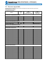
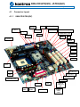
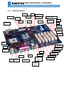
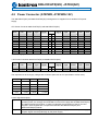
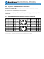
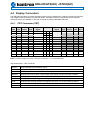
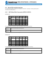
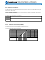
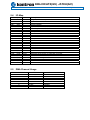
1
886LCD/ATX(GV) -/ATXU(GV) KTD-00647-E Public User Manual Date: 2009-01-14 User Manual for the Mother Boards: 886LCD/ATX(GV) 886LCD/ATXU(GV) Page 1 of 71 886LCD/ATX(GV) -/ATXU(GV) KTD-00647-E Public User Manual Date: 2009-01-14 Page 2 of 71 Document revision history. Revision Date By E D th Jan. 14 2009 May 30th 2008 MLA MLA C Feb 8th, 2007 MLA B 1.0 0.1 June 6th, 2006 Mar 13th, 2006 Dec 9th, 2005 MLA PJA PJA Comment Minor corrections. PXE/RPL selection added to BIOS. Battery type updated and Battery load information added. Correction: Processor support table. JP3 connector included. Removal of “PCI Slot-3/4/5 IRQ Preference” Many minor corrections. Release version. First preliminary manual version. Copyright Notice: Copyright © 2006, KONTRON Technology A/S, ALL RIGHTS RESERVED. No part of this document may be reproduced or transmitted in any form or by any means, electronically or mechanically, for any purpose, without the express written permission of KONTRON Technology A/S. Trademark Acknowledgement: Brand and product names are trademarks or registered trademarks of their respective owners. Disclaimer: KONTRON Technology A/S reserves the right to make changes, without notice, to any product, including circuits and/or software described or contained in this manual in order to improve design and/or performance. Specifications listed in this manual are subject to change without notice. KONTRON Technology assumes no responsibility or liability for the use of the described product(s), conveys no license or title under any patent, copyright, or mask work rights to these products, and makes no representations or warranties that these products are free from patent, copyright, or mask work right infringement, unless otherwise specified. Applications that are described in this manual are for illustration purposes only. KONTRON Technology A/S makes no representation or warranty that such application will be suitable for the specified use without further testing or modification. 886LCD/ATX(GV) -/ATXU(GV) KTD-00647-E Public User Manual Date: 2009-01-14 Page 3 of 71 Life Support Policy KONTRON Technology’s PRODUCTS ARE NOT FOR USE AS CRITICAL COMPONENTS IN LIFE SUPPORT DEVICES OR SYSTEMS WITHOUT EXPRESS WRITTEN APPROVAL OF THE GENERAL MANAGER OF KONTRON Technology A/S. As used herein: 1. Life support devices or systems are devices or systems which, (a) are intended for surgical implant into body, or (b) support or sustain life and whose failure to perform, when properly used in accordance with instructions for use provided in the labeling, can be reasonably expected to result in significant injury to the user. 2. A critical component is any component of a life support device or system whose failure to perform can be reasonably expected to cause the failure of the life support device or system, or to affect its safety or effectiveness. KONTRON Technology Technical Support and Services If you have questions about installing or using your KONTRON Technology Product, check this User’s Manual first – you will find answers to most questions here. To obtain support, please contact your local Distributor or Field Application Engineer (FAE). Before Contacting Support: Please be prepared to provide as much information as possible: CPU Board 1. Type. 2. Part-number (Number starting with “6”). 3. Serial Number. Configuration 1. CPU Type, Clock speed. 2. DRAM Type and Size. 3. BIOS Revision (Find the Version Info in the BIOS Setup in the Kontron Section). 4. BIOS Settings different than Default Settings (Refer to the Software Manual). System 1. O/S Make and Version. 2. Driver Version numbers (Graphics, Network, and Audio). 3. Attached Hardware: Harddisks, CD-rom, LCD Panels etc. 886LCD/ATX(GV) -/ATXU(GV) KTD-00647-E Public User Manual Date: 2009-01-14 Page 4 of 71 Table of contents: 1. INTRODUCTION .....................................................................................................................................7 2. INSTALLATION PROCEDURE ..............................................................................................................8 2.1 Installing the board............................................................................................................................8 2.2 Requirement according to EN60950: ...............................................................................................9 3. SYSTEM SPECIFICATION ...................................................................................................................10 3.1 Component main data .....................................................................................................................10 3.2 Processor support table..................................................................................................................12 3.3 System Memory support .................................................................................................................14 3.4 System overview ..............................................................................................................................15 3.5 Power Consumption ........................................................................................................................16 4. CONNECTOR DEFINITIONS................................................................................................................17 4.1 Connector layout..............................................................................................................................18 4.1.1 886LCD/ATXU(GV) ....................................................................................................................18 4.1.2 886LCD/ATX(GV) .......................................................................................................................19 4.2 Power Connector (ATXPWR, ATXPWR+12V)................................................................................20 4.3 Keyboard and PS/2 mouse connectors .........................................................................................21 4.3.1 Stacked MINI-DIN keyboard and mouse Connector (MSE & KBD) ...........................................21 4.4 Display Connectors .........................................................................................................................22 4.4.1 CRT Connector (CRT) ................................................................................................................22 4.4.2 (AGP)/DVO connector ................................................................................................................23 4.5 Parallel ATA harddisk interface......................................................................................................25 4.5.1 IDE Hard Disk Connector (IDE_P) .............................................................................................26 4.5.2 IDE Hard Disk Connector (IDE_S) .............................................................................................26 4.6 Serial ATA harddisk interface.........................................................................................................27 4.6.1 SATA Hard Disk Connector (SATA0, SATA1) ...........................................................................27 4.7 Floppy Disk Connector (FDC1).......................................................................................................28 4.8 Printer Port Connector (PRINTER).................................................................................................29 4.9 Serial Ports .......................................................................................................................................30 4.9.1 Serial Port Com1 DB9 Connector...............................................................................................30 4.9.2 Serial Port Com2 Pin Header Connectors..................................................................................30 4.10 Ethernet connector. .....................................................................................................................31 4.10.1 Ethernet connector (ETHER)......................................................................................................31 4.11 USB Connector (USB)..................................................................................................................32 4.11.1 USB Connector 0/1 (USB0/1).....................................................................................................32 4.11.2 USB Connector 2/3 (USB2/3).....................................................................................................33 4.11.3 USB Connector 4/5 (USB4/5).....................................................................................................33 886LCD/ATX(GV) -/ATXU(GV) KTD-00647-E Public User Manual Date: 2009-01-14 Page 5 of 71 4.12 Audio Connector ..........................................................................................................................34 4.12.1 Audio Line-in, Line-out and Microphone.....................................................................................34 4.12.2 CD-ROM Audio input (CDROM).................................................................................................34 4.13 Fan connectors, CPU FAN, CHASSIS FAN, PWR FAN. ............................................................35 4.14 The Clear CMOS Jumper, Clr-CMOS. .........................................................................................36 4.15 Front Side Bus Speed, FSB.........................................................................................................36 4.16 Case Open, S1 ..............................................................................................................................37 4.17 Trusted Platform Module (TPM) connector, CN7 (unsupported). ...........................................37 4.18 Front Panel connector, CN5. .......................................................................................................38 4.19 GAME / MIDI Connector, CN6......................................................................................................39 4.20 IR Connector (IR1)........................................................................................................................39 4.21 WOL Connector (W.O.L). .............................................................................................................40 4.22 JP3 (optional)................................................................................................................................40 4.23 PCI Slot 1, Slot 2 and Slot 3 connectors. ..................................................................................41 4.23.1 PCI Slot Connector ....................................................................................................................41 4.23.2 Signal Description –PCI Slot Connector.....................................................................................42 4.23.3 886LCD/ATX(GV) and 886LCD/ATXU(GV) PCI IRQ & INT routing ..........................................43 5. SYSTEM RESOURCES ........................................................................................................................44 5.1 Memory map .....................................................................................................................................44 5.2 PCI devices .......................................................................................................................................44 5.3 Interrupt Usage ................................................................................................................................45 5.4 I/O Map ..............................................................................................................................................46 5.5 DMA Channel Usage........................................................................................................................46 6. OVERVIEW OF BIOS FEATURES .......................................................................................................47 6.1.1 System Management BIOS (SMBIOS / DMI) .............................................................................47 6.1.2 Legacy USB Support ..................................................................................................................47 7. BIOS CONFIGURATION / SETUP .......................................................................................................48 7.1 Introduction ......................................................................................................................................48 7.2 Main Menu.........................................................................................................................................48 7.3 Advanced Menu................................................................................................................................49 7.3.1 Advanced settings – CPU Configuration ....................................................................................49 7.3.2 Advanced settings – IDE Configuration......................................................................................50 7.3.3 Advanced settings – Floppy Configuration .................................................................................52 7.3.4 Advanced settings – SuperIO Configuration ..............................................................................53 7.3.5 Advanced settings – Hardware Health Configuration ................................................................54 7.3.6 Advanced settings – ACPI Configuration ...................................................................................55 7.3.7 Advanced settings – General ACPI Configuration .....................................................................56 7.3.8 Advanced settings – Advanced ACPI Configuration ..................................................................57 7.3.9 Advanced settings – USB Configuration ....................................................................................58 886LCD/ATX(GV) -/ATXU(GV) KTD-00647-E 7.3.10 7.4 Public User Manual Date: 2009-01-14 Page 6 of 71 Advanced settings – USB Mass Storage Device Configuration.................................................59 PCIPnP Menu....................................................................................................................................60 7.5 Boot Menu.........................................................................................................................................61 7.5.1 Boot – Boot Settings Configuration ............................................................................................62 7.6 Security Menu...................................................................................................................................63 7.7 Chipset Menu....................................................................................................................................64 7.7.1 Advanced Chipset Settings – Intel Brookdale-G NorthBridge Configuration .............................65 7.7.2 Advanced Chipset Settings – SouthBridge Configuration ..........................................................66 7.8 Power Menu......................................................................................................................................67 7.9 Exit Menu ..........................................................................................................................................68 7.10 AMI BIOS Beep Codes .................................................................................................................69 8. OS SETUP.............................................................................................................................................70 9. WARRANTY..........................................................................................................................................71 886LCD/ATX(GV) -/ATXU(GV) KTD-00647-E 1. Public User Manual Date: 2009-01-14 Page 7 of 71 Introduction This manual describes the 886LCD/ATX(GV) and 886LCD/ATXU(GV) boards made by KONTRON Technology A/S. The boards will also be denoted 886LCD-GV family if no differentiation is required. All boards are to be used with the Intel® Pentium® 4, Intel Celeron® and Intel® Celeron® D Processors. Use of this manual implies a basic knowledge of PC-AT hard- and software. This manual is focused on describing the 886 Board’s special features and is not intended to be a standard PC-AT textbook. New users are recommended to study the short installation procedure stated in chapter 2 before switchingon the power. 886LCD/ATX(GV) -/ATXU(GV) KTD-00647-E Public User Manual 2. Installation procedure 2.1 Installing the board Date: 2009-01-14 Page 8 of 71 To get the board running, follow these steps. In some cases the board shipped from KONTRON Technology has CPU, DDR DRAM and Cooler mounted. In this case Step 2-4 can be skipped. 1. Turn off the power supply. ! Warning: Do not use Power Supply without voltage monitoring watchdog, which is standard feature in ATX Power Supplies. Running the board without 3.3V connected will damage the board after a few minuttes. 2. Insert the DIMM DDR 184pin DRAM module(s). Be careful to push it in the slot(s) before locking the tabs. For a list of approved DDR DRAM modules contact your Distributor or FAE. DIMM 184pin DRAM modules are supported. 3. Install the processor. The CPU is keyed and will only mount in the CPU socket in one way. Use the handle to open/ close the CPU socket. Intel® Pentium® 4, Celeron® and Celeron® D processors are supported. 4. Use heat paste or adhesive pads between CPU and cooler and connect the Fan electrically to the FAN3 connector. (See chapter 4.1 for identifying the FAN3 connector). 5. Insert all external cables for hard disk, keyboard etc. except for flat panel. A CRT monitor must be connected in order to change CMOS settings to flat panel support (with ADD-DVO module). To achieve UDMA-66/100/133 performance on the IDE interface, 80poled UDMA cables must be used. 6. Connect power supply to the board by the ATXPWR connector. 7. Turn on the ATX power supply. 8. The PWRSW must be toggled to start the Power supply; this is done by shorting pins pins 19 and 21 on the CN5 connector (see Connector description). A “normally open” switch can be connected via the CN5 connector. 9. Enter the BIOS setup by pressing the “F2” key during boot up. Refer to the Software Manual for details on BIOS setup. Note: To clear all CMOS settings, including Password protection, move the JP6 jumper (with or without power) for approximately 1 minute. Alternatively turn off power and remove the battery for 1 minute, but be careful to orientate the battery corretly when reinserted. 886LCD/ATX(GV) -/ATXU(GV) KTD-00647-E 2.2 Public User Manual Date: 2009-01-14 Page 9 of 71 Requirement according to EN60950: Users of 886LCD-GV boards should take care when designing chassis interface connectors in order to fulfill the EN60950 standard: When an interface/connector has a VCC (or other power) pin, which is directly connected to a power plane like the VCC plane: To protect the external power lines of peripheral devices the customer has to take care about: • That the wires have the right diameter to withstand the maximum available power. • That the enclosure of the peripheral device fulfils the fire protecting requirements of IEC/EN 60950. Lithium Battery precautions: CAUTION! VORSICHT! Danger of explosion if battery is incorrectly replaced. Explosionsgefahr bei unsachgemäßem Austausch der Batterie. Ersatz nur durch den selben oder einen vom Hersteller empfohlenen gleichwertigen Typ. Entsorgung gebrauchter Batterien nach Angaben des Herstellers. Replace only with same or equivalent type recommended by manufacturer. Dispose of used batteries according to the manufacturer’s instructions. ADVARSEL! ADVARSEL Lithiumbatteri – Eksplosionsfare ved fejlagtig håndtering. Udskiftning må kun ske med batteri af samme fabrikat og type. Levér det brugte batteri tilbage til leverandøren. Eksplosjonsfare ved feilaktig skifte av batteri. Benytt samme batteritype eller en tilsvarende type anbefalt av apparatfabrikanten. Brukte batterier kasseres i henhold til fabrikantens instruksjoner. VARNING VAROITUS Explosionsfara vid felaktigt batteribyte. Använd samma batterityp eller en ekvivalent typ som rekommenderas av apparattillverkaren. Kassera använt batteri enligt fabrikantens instruktion. Paristo voi räjähtää, jos se on virheellisesti asennettu. Vaihda paristo ainoastaan laltevalmistajan suosittelemaan tyyppiln. Hävitä käytetty paristo valmistajan ohjeiden mukaisesti. 886LCD/ATX(GV) -/ATXU(GV) KTD-00647-E 3. Public User Manual Date: 2009-01-14 Page 10 of 71 System specification 3.1 Component main data The table below summarises the features of the 886LCD-GV embedded motherboards. Form factor Processor Memory Chipset Video 886LCD/ATXU(GV): uATX (244,1 x 305,0 mm) 886LCD/ATX(GV): ATX (190,5 x 304,0 mm) • Support for Intel® Pentium® 4, Intel Celeron® and Intel® Celeron® D Processors in mPGA478 socket with 400MHz/ 533MHz system bus. • 0.13 micron and 90nm Architecture support • L2 cache: 128KB, 256KB and 512KB • 2x184pin DDR SDRAM Dual Inline Memory Module (DIMM) sockets. • Support for DDR 266 (PC2100). DRAM supporting higher speeds: DDR 333 (PC2700) and DDR 400 (PC3200) may be used after qualification testing. • Support for up to 2GB of system memory • ECC not supported Intel 845GV Chipset consisting of: • Intel® 82845GV Graphics and Memory Controller Hub (GMCH) • Intel® 82801DB I/O Controller Hub 4 (ICH4) • 4 Mbit Firmware Hub (FWH) for BIOS • Intel Extreme Graphics controller • Video memory support: maximum 64MB with more than 128MB DDR SDRAM installed. • The GMCH has an integrated 350 MHz RAMDAC that can directly drive a progressive scan analog monitor up to a resolution of 2048x1536 at 60 Hz. • The GMCH provides two multiplexed Digital Video Out Ports (DVOs) through the onboard AGP 2.0, 1.5V connector that are can drive a 165 MHz pixel clock. o DVI DVO ADD, CRT DVO ADD and LVDS DVO ADD cards supported Note: Only ADD cards are supported , AGP cards are not supported. Audio I/O Control Peripheral interfaces LAN Support BIOS Audio, AC97 version 2.3 subsystem using the Realtek ALC655 codec • Line-out • Line-in • CDROM in • Microphone Winbond W83627HG LPC Bus I/O Controller • USB host interface; 3 host controllers and supports 6 USB ports; includes a EHCI high-speed 2.0 USB controller. USB legacy keyboard function supported. • Two Serial ports (RS232). Port 2 can be set to operate in normal, IrDA or ASKIR mode • One Parallel port, SPP/EPP/ECP • One Floppy port • Two Serial ATA 150 IDE interfaces. • Two Parallel ATA IDE interfaces with UDMA 33, ATA-66, ATA-100 support • PS/2 keyboard and mouse ports • Game/Midi port 1x 10/100Mbits/s LAN subsystem using the Realtek RTL8100C LAN controllers. PXE netboot supported. Wake On LAN (WOL) supported. • Kontron Technology / AMI BIOS (core version 8.00) • Support for Advanced Configuration and Power Interface (ACPI 1.0, 2.0), Plug and Play o Suspend To Ram o Suspend To Disk • SW Watchdog not supported by BIOS • Secure CMOS/ OEM Setup Defaults • “Always On” BIOS power setting • SATA RAID Support (RAID modes 0 and 1) 886LCD/ATX(GV) -/ATXU(GV) KTD-00647-E Instantly Available PC Technology Expansion Capabilities Hardware Monitor Subsystem Operating Systems Support Environmental Conditions Public • • User Manual Date: 2009-01-14 Page 11 of 71 PCI Rev 2.2 compliant with support for 33 MHz PCI operations Suspend to RAM support • PCI Bus routed to PCI slot(s) (PCI Local Bus Specification Revision 2.2) • 3 x PCI bus with Bus master mode on 886LCD/ATXU(GV) board • 6 x PCI bus with Bus master mode on 886LCD/ATX(GV) board • 2 x DVO ports for ADD card expansion • LPC Bus routed to CN7 connector / Trusted Platform Module Header • Fan monitoring: CPU FAN, CHASSIS FAN, PWR FAN • Thermal monitoring: CPU die temperature, System temperature and External temperature input (routed to JP3 connector). • Voltage monitoring • Intrusion detect input (JP6) • SMI violations (BIOS) on HW monitor not supported. Supported by API (Windows) • WinXP • Win2000 • Win2003 • WinXP Embedded (limitations may apply) • WinCE.net (limitations may apply) • Linux: Feodora Core 3, Suse 9.2 (limitations may apply) Operating: 0°C – 60°C operating temperature (forced cooling). It is the customer’s responsibility to provide sufficient airflow around each of the components to keep them within allowed temperature range. Storage: -20°C – 70°C and 5% - 95% relative humidity (non-condensing) Electro Static Discharge (ESD) / Radiated Emissions (EMI): All Peripheral interfaces intended for connection to external equipment are ESD/ EMI protected. EN 61000-4-2:2000 ESD Immunity EN55022:1998 class B Generic Emission Standard. Safety: UL 60950-1:2003, First Edition CSA C22.2 No. 60950-1-03 1st Ed. April 1, 2003 Product Category: Information Technology Equipment Including Electrical Business Equipment Product Category CCN: NWGQ2, NWGQ8 File number: E194252 Theoretical MTBF: 129679 hours (14,5 years). Calculation based on Telcordia SR-332 method. Restriction of Hazardeous Substances (RoHS): 886LCD/ATX(GV) and 886LCD/ATXU(GV) boards are RoHS compliant. Battery Capacitor utilization: No Tantal capacitors on board. Only Japanese brand Aluminium capacitors rated for 100 ºC used on board. Exchangeable 3.0V Lithium battery for onboard Real Time Clock and CMOS RAM. Manufacturer Panasonic / PN CR2032NL/LE or CR-2032L/BE. Expected minimum 5 years retention varies depending on temperature, actual application on/off rate and variation within chipset and other components. Approximately current draw is 3.7µA (no PSU connected). CAUTION: Danger of explosion if the battery is incorrectly replaced. Replace only with the same or equivalent type recommended by the manufacturer. Dispose of used batteries according to the manufacturer’s instructions. 886LCD/ATX(GV) -/ATXU(GV) KTD-00647-E 3.2 Public User Manual Date: 2009-01-14 Page 12 of 71 Processor support table. 886LCD/ATX(GV) and 886LCD/ATX(GV) boards are designed to support the following processors: Intel® Pentium® 4 Processors Intel® Celeron® D Processors Intel Celeron® Processors Speed Cache size Intel Single Pack Product Order Code Intel OEM Product Order Code Intel® Pentium 4® Embedded Processors 2.0A GHZ 400MHz FSB 2.40 GHZ 533MHz FSB 2.60 GHZ 400MHz FSB 2.80 GHZ 400MHz FSB 512K 512K 512K 512K RK80532PC041512 RK80532PE056512 RK80532PC064512 RK80532PE072512 128K 128K RK80532RC041128 RK80532RC060128 Intel® Celeron® Embedded Processors 2.00 GHZ, 400MHz FSB 2.50 GHZ, 400MHz FSB Intel® Celeron® D Embedded Processors 2.80 GHz, 533MHz FSB 256K BX80546RE2800C RK80546RE072256 Intel® Pentium 4® Processors 1.60 GHZ, 400MHz FSB 1.60 GHZ, 400MHz FSB 1.80 GHZ, 400MHz FSB 1.80 GHZ, 400MHz FSB 2.00 GHZ, 400MHz FSB 2.20 GHZ, 400MHz FSB 2.26 GHZ, 533MHz FSB 2.40 GHZ, 400MHz FSB 2.40 GHZ, 533MHz FSB 2.50 GHZ, 400MHz FSB 2.53 GHZ, 533MHz FSB 2.60 GHZ, 400MHz FSB 2.66 GHZ, 533MHz FSB 2.80 GHZ, 533MHz FSB 3.06 GHZ, 533MHz FSB, HT* 512K 512K 512K 512K 512K 512K 512K 512K 512K 512K 512K 512K 512K 512K 512K RK80534PC025512 BX80532PC1600D BX80532PC1800D BX80532PC2000D BX80532PC2200D BX80532PE2266D BX80532PC2400D BX80532PE2400D BX80532PC2500D BX80532PE2533D BX80532PC2600D BX80532PE2667D BX80532PE2800D BX80532PE3066D RK80534PC033512 RK80532PC033512 RK80532PC041512 RK80532PC049512 RK80532PE051512 RK80532PC056512 RK80532PE056512 RK80532PC060512 RK80532PE061512 RK80532PC064512 RK80532PE067512 RK80532PE072512 RK80532PE083512 Intel® Celeron® Processors 1.70 GHZ, 400MHz FSB 1.80 GHZ, 400MHz FSB 2.00 GHZ, 400MHz FSB 2.10 GHZ, 400MHz FSB 2.20 GHZ, 400MHz FSB 2.30 GHZ, 400MHz FSB 2.30 GHZ, 400MHz FSB 2.40 GHZ, 400MHz FSB 2.50 GHZ, 400MHz FSB 2.60 GHZ, 400MHz FSB 2.70 GHZ, 400MHz FSB 2.80 GHZ, 400MHz FSB 128K 128K 128K 128K 128K 128K 128K 128K 128K 128K 128K 128K BX80531P170G128 BX80531P180G128 BX80532RC2000B BX80532RC2100B BX80532RC2200B BX80532RC2300B BX80532RC2400B BX80532RC2500B BX80532RC2600B BX80532RC2700B BX80532RC2800B RK80531RC029128 RK80531RC033128 RK80532RC041128 RK80532RC045128 RK80532RC049128 RK80532RC052128 B80532RC052128 RK80532RC056128 RK80532RC060128 RK80532RC064128 RK80532RC068128 RK80532RC072128 886LCD/ATX(GV) -/ATXU(GV) KTD-00647-E Public Speed User Manual Cache size Date: 2009-01-14 Intel Single Pack Product Order Code Page 13 of 71 Intel OEM Product Order Code Intel® Celeron® D Processors 3.20 GHz, 533MHz FSB 3.06 GHz, 533MHz FSB 2.93 GHz, 533MHz FSB 2.80 GHz, 533MHz FSB 2.66 GHz, 533MHz FSB 2.53 GHz, 533MHz FSB 2.40 GHz, 533MHz FSB 2.26 GHz, 533MHz FSB 2.13 GHz, 533MHz FSB * HT = Hyper Threading support 256K 256K 256K 256K 256K 256K 256K 256K 256K BX80546RE3200C BX80546RE3066C BX80546RE2933C BX80546RE2800C BX80546RE2667C BX80546RE2533C BX80546RE2400C BX80546RE2267C BX80546RE2130C RK80546RE088256 RK80546RE083256 RK80546RE077256 RK80546RE072256 RK80546RE067256 RK80546RE061256 RK80546RE056256 RK80546RE051256 RK80546RE046256 886LCD/ATX(GV) -/ATXU(GV) KTD-00647-E 3.3 Public User Manual Date: 2009-01-14 Page 14 of 71 System Memory support The 886LCD/ATX(GV) and 886LCD/ATXU(GV) boards have two onboard DIMM sockets and support the following memory features: • • • • • • • 2.5V (only) 184-pin DDR SDRAM DIMMs with gold-plated contacts Supports up to two single-sided and/or double-sided DIMMs (four rows populated) with unbuffered PC1600/PC2100 DDR-SDRAM Supports 64 Mbit, 128 Mbit, 256 Mbit and 512 Mbit technologies for x8 and x16 width devices. Maximum of 2 Gbytes system memory by using 512 Mbit technology devices (double sided) Supports 200 MHz and 266 MHz DDR devices 64-bit data interface ECC not supported with the Intel 845GV chipset The installed DDR SDRAM should support the Serial Presence Detect (SPD) data structure. This allows the BIOS to read and configure the memory controller for optimal performance. If non-SPD memory is used, the BIOS will attempt to configure the memory settings, but performance and reliability may be impacted. In general DDR SDRAM with higher speeds than 266MHz may be used (e.g. 333MHz or 400MHz), but it is recommended to run a qualification test before use or to use Kontron Technology validated DDR SDRAM. 886LCD/ATX(GV) -/ATXU(GV) KTD-00647-E 3.4 Public User Manual Date: 2009-01-14 Page 15 of 71 System overview The block diagram below shows the architecture and main components of the 886LCD boards. The two key components on the board are the Intel® 845GV and Intel® ICH4 Embedded Chipsets. 886LCD/ATX(GV) -/ATXU(GV) KTD-00647-E 3.5 Public User Manual Date: 2009-01-14 Page 16 of 71 Power Consumption This section describes static and dynamic power consumption on the 886LCD/ATXU(GV) board in a specific configuration: • • • • • 886LCD/ATXU(GV) P4, 2.0GHz, 400MHz FSB, 256MByte L2 cache P4 cooler 256Mbyte of PC2100 / 266MHz DDR SDRAM VGA monitor, Keyboard and mouse inserted Wire colour Yellow (CPU) Voltage 12,00 V /[A] State XP Idle DC XP Idle AC XP Idle power XP Full Load DC XP Full Load AC XP Full Load power Red Orange Yellow Blue Purple White 5,00 V /[A] 3,30 V /[A] 12,00 V -12,00 V 5,00 V /[A] /[A] /[A] -5,00 V /[A] 0,74 0,06 0,24 0,00 2,65 0,05 0,34 0,07 0,02 0,03 0,06 0,04 0,03 0,05 3,60 0,38 0,29 0,02 3,66 0,29 0,34 0,08 0,03 0,03 0,04 0,04 0,04 0,04 Total Power /[W] 23,60 2,54 26,13 61,57 7,34 68,91 886LCD/ATX(GV) -/ATXU(GV) KTD-00647-E 4. Public User Manual Date: 2009-01-14 Page 17 of 71 Connector Definitions The following sections provide pin definitions and detailed description of all on-board connectors. . The connector definitions follow the following notation: Column name Description Pin Shows the pin-numbers in the connector. The graphical layout of the connector definition tables is made similar to the physical connectors. Signal The mnemonic name of the signal at the current pin. The notation “XX#” states that the signal “XX” is active low. Type AI : Analog Input. AO : Analog Output. I: Input, TTL compatible if nothing else stated. IO : Input / Output. TTL compatible if nothing else stated. IOT : Bi-directional tristate IO pin. IS : Schmitt-trigger input, TTL compatible. IOC : Input / open-collector Output, TTL compatible. NC : Pin not connected. O: Output, TTL compatible. OC : Output, open-collector or open-drain, TTL compatible. OT : Output with tri-state capability, TTL compatible. LVDS: Low Voltage Differential Signal. PWR : Power supply or ground reference pins. Ioh: Typical current in mA flowing out of an output pin through a grounded load, while the output voltage is > 2.4 V DC (if nothing else stated). Iol: Typical current in mA flowing into an output pin from a VCC connected load, while the output voltage is < 0.4 V DC (if nothing else stated). Pull U/D On-board pull-up or pull-down resistors on input pins or open-collector output pins. Note Special remarks concerning the signal. The abbreviation TBD (To Be Determined) is used for specifications which are not available yet or which are not sufficiently specified by the component vendors. 886LCD/ATX(GV) -/ATXU(GV) KTD-00647-E 4.1 Public User Manual Date: 2009-01-14 Page 18 of 71 Connector layout 4.1.1 886LCD/ATXU(GV) FSB DIMM2 FLOPPY CASE OPEN Clr-CMOS DIMM1 FRONT PANEL, CN5 IDE_P IDE_S GAME/ MIDI, CN6 TPM WOL IR ATXPWR USB2/3 (AGP)/DVO COM2 FAN1 SATA1 SATA0 FAN3 JP3 PCI SLOT 3 PCI SLOT 2 FAN2 PCI SLOT 1 ATXPWR +12V CDROM CRT COM1 MSE KBD USB0 USB1 PRINTER LINE-IN LINE-OUT MIC ETHER USB4 USB5 886LCD/ATX(GV) -/ATXU(GV) KTD-00647-E 4.1.2 Public User Manual Date: 2009-01-14 Page 19 of 71 886LCD/ATX(GV) FSB DIMM2 DIMM1 FLOPPY IDE_P IDE_S CASE OPEN Clr-CMOS TPM USB2/3 FRONT PANEL, CN WOL GAME/ MIDI, CN6 IR ATXPWR COM2 (AGP)/DVO SATA1 SATA0 FAN3 PCI SLOT 6 FAN2 PCI SLOT 5 ATXPWR +12V PCI SLOT 4 FAN1 PCI SLOT 3 CRT COM1 MSE KBD USB0 USB1 CDROM PRINTER PCI SLOT 2 LINE-IN LINE-OUT MIC ETHER USB4 USB5 PCI SLOT 1 886LCD/ATX(GV) -/ATXU(GV) KTD-00647-E Public User Manual Date: 2009-01-14 Page 20 of 71 4.2 Power Connector (ATXPWR, ATXPWR+12V) The 886LCD/ATX(GV) and 886LCD/ATXU(GV) is designed to be supplied from a standard ATX power supply. ATX Power Connector 886LCD/ATX(GV) and 886LCD/ATXU(GV) Pull U/D Ioh/Iol Type PWR PWR 4K7 I PWR PWR PWR PWR PWR PWR PWR Note: -5V supply is not used onboard. Note PIN Signal +12V SB5V P_OK GND 5V GND 5V GND 3V3 3V3 10 9 8 7 6 5 4 3 2 1 20 19 18 17 16 15 14 13 12 11 Signal 5V 5V -5V GND GND GND PSON# GND -12V 3V3 Type PWR PWR PWR PWR PWR PWR OC PWR PWR PWR Ioh/Iol - Pull U/D - Type PWR PWR Ioh/Iol - Pull U/D - Note 1 +12V Power Connector 886LCD/ATX(GV) and 886LCD/ATXU(GV) Note Pull U/D - PIN Ioh/Iol - Type PWR PWR Signal GND GND 4 2 3 1 Signal +12V +12V Note The requirements to the supply voltages are as follows (also refer to ATX specification version 2.03): Supply Min Max Tolerance 3V3 3.14V 3.46V +/-5% 5V 4.75V 5.25V +/-5% SB5V 4.75V 5.25V +/-5% +12V 11.4V 12.6V +/-5% –12V –13.2V –10.8V +/-10% Control signal description: P_OK Active high signal from the power supply indicating that the 5V and 3V3 supplies are within operating limits. It is strongly recommended to use an ATX supply with the 886LCD/ATX(GV) and 886LCD/ATXU(GV) boards, in order to implement the supervision of the 5V and 3V3 supplies. These supplies are not supervised onboard the 886LCD/ATX(GV) and 886LCD/ATXU(GV) boards. PS_ON# Active low open drain signal from the board to the power supply to turn on the power supply outputs. Signal must be pulled high by the power supply. 886LCD/ATX(GV) -/ATXU(GV) KTD-00647-E Public User Manual Date: 2009-01-14 Page 21 of 71 4.3 Keyboard and PS/2 mouse connectors Attachment of a keyboard or PS/2 mouse adapter can be done through the stacked PS/2 mouse and keyboard connector (MSE & KBD). Both interfaces utilize open-drain signaling with on-board pull-up. The PS/2 mouse and keyboard is supplied from 5V_STB when in standby mode in order to enable keyboard or mouse activity to bring the system out from power saving states. The supply is provided through a 1.1A resetable fuse. 4.3.1 Note Stacked MINI-DIN keyboard and mouse Connector (MSE & KBD) Pull U/D Ioh/Iol Type Signal PIN - - - NC 6 - - PWR 5V/SB5V 4 - - - NC - NC 6 4 - - PWR 5V/SB5V - - - NC 2 2 Signal Type Ioh/Iol Pull U/D 5 MSCLK IOC TBD 2K2 3 GND PWR - - MSDAT IOC TBD 2K2 5 KBDCLK IOC TBD 2K2 3 GND PWR - - KBDDAT IOC TBD 2K2 1 1 Signal Description – Keyboard & and mouse Connector (MSE & KBD), see below. Note 886LCD/ATX(GV) -/ATXU(GV) KTD-00647-E Public User Manual Date: 2009-01-14 Page 22 of 71 4.4 Display Connectors The 886LCD board family provides onboard two basic types of interfaces to a display: Analog CRT interface and a digital interface typically used with flat panels. The digital interface to flat panels can be achieved through the DVO port available on the AGP connector by using a dedicated ADD card. 4.4.1 Note CRT Connector (CRT) Pull U/D PIN Ioh/Iol Type Signal 6 /75R * A0 RED 1 11 7 /75R * A0 GREEN 2 12 8 /75R * A0 BLUE 3 13 9 - - - NC 4 - - PWR DIG-GND 5 14 10 15 Signal Type Ioh/Iol Pull U/D ANA-GND PWR - - NC ANA-GND DDCDAT ANA-GND HSYNC 5V VSYNC DIG-GND DDCCLK PWR IO PWR O PWR O PWR IO TBD TBD TBD TBD 2K7 - Note 2K7 Note 1: The 5V supply in the CRT connector is fused by a 1.1A reset-able fuse. Signal Description - CRT Connector: HSYNC CRT horizontal synchronization output. VSYNC CRT vertical synchronization output. DDCCLK Display Data Channel Clock. Used as clock signal to/from monitors with DDC interface. DDCDAT Display Data Channel Data. Used as data signal to/from monitors with DDC interface. RED Analog output carrying the red color signal to the CRT. For 75 Ohm cable impedance. GREEN Analog output carrying the green color signal to the CRT. For 75 Ohm cable impedance. BLUE Analog output carrying the blue color signal to the CRT. For 75 Ohm cable impedance. DIG-GND Ground reference for HSYNC and VSYNC. ANA-GND Ground reference for RED, GREEN, and BLUE. 1 886LCD/ATX(GV) -/ATXU(GV) KTD-00647-E 4.4.2 Public User Manual Date: 2009-01-14 Page 23 of 71 (AGP)/DVO connector The 886LCD/ATX(GV) and 886LCD/ATXU(GV) boards are equipped with the Intel 845GV chipset. The GV chipset does not support AGP output, but only DVO output. Note Type PWR PWR PWR PWR I PWR I PWR I I PWR I I PWR PWR PWR PWR PWR PWR PWR PWR PWR PWR PWR PWR PWR PWR PWR Signal Type OVRCNT +5V +5V NC GND INTB AGPCLK GREQ +3.3V ST0 ST2 RBF GND RSVD ADD_ID0 +3.3V ADD_ID2 ADD_RS GND ADD_ID4 ADD_ID6 RSVD GND 3V3AUX +3.3V DVOC_Fld/Stl DVOC_D10 +3.3V DVOC_D8 DVOC_D6 GND DVOC_Clk+ DVOC_D4 +1.5V DVOC_D2 DVOC_D0 GND DVOC_Hsync ADD_RS +1.5V M_I2CClk Signal B1 B2 B3 B4 B5 B6 B7 B8 B9 B10 B11 B12 B13 B14 B15 B16 B17 B18 B19 B20 B21 B22 B23 B24 B25 B26 B27 B28 B29 B30 B31 B32 B33 B34 B35 B36 B37 B38 B39 B40 B41 PIN A1 A2 A3 A4 A5 A6 A7 A8 A9 A10 A11 A12 A13 A14 A15 A16 A17 A18 A19 A20 A21 A22 A23 A24 A25 A26 A27 A28 A29 A30 A31 A32 A33 A34 A35 A36 A37 A38 A39 A40 A41 +12V TYPEDET RSVD NC GND INTA RSTGGNT +3.3V ST1 RSVD PIPE GND WBF ADD_ID1 +3.3V ADD_ID3 ADD_RS GND ADD_ID5 ADD_ID7 RSVD GND RSVD +3.3V DVOBC_IntrDVOC_D11 +3.3V DVOC_D9 DVOC_D7 GND DVOC_ClkDVOC_D5 +1.5V DVOC_D3 DVOC_D1 GND DVOC_BlankDVOC_Vsync +1.5V M_DVI_Data PWR M_I2CData +1.5V GPERR GND GSERR DVOB_Blank+1.5V DVOB_Fld/Stl DVOB_D10 GND DVOB_D8 DVOB_D6 +1.5V DVOB_Clk+ DVOB_D4 GND DVOB_D2 DVOB_D0 +1.5V DVOB-Vsync VREFCG B46 B47 B48 B49 B50 B51 B52 B53 B54 B55 B56 B57 B58 B59 B60 B61 B62 B63 B64 B65 B66 A46 A47 A48 A49 A50 A51 A52 A53 A54 A55 A56 A57 A58 A59 A60 A61 A62 A63 A64 A65 A66 M_DVI_Clk M_DDCData PME GND ADD_Detect M_DDCClk +1.5V DVOBC_ClkInt DVOB_D11 GND DVOB_D9 DVOB_D7 +1.5V DVOB_ClkDVOB_D5 GND DVOB_D3 DVOB_D1 +1.5V DVOB_Hsync NC PWR PWR I PWR I I PWR I PWR I I PWR PWR PWR PWR PWR PWR PWR PWR PWR PWR PWR PWR PWR Note 886LCD/ATX(GV) -/ATXU(GV) KTD-00647-E Public User Manual Date: 2009-01-14 Page 24 of 71 Signal Description – (AGP)/DVO Connector: Signal DVOB_CLK; DVOB_CLK# DVOB_D[11:0] DVOB_HSYNC DVOB_VSYNC DVOB_BLANK# DVOBC_CLKINT# DVOB_FLDSTL DVOC_CLK; DVOC_CLK# DVOC_D[11:0] DVOC_HSYNC DVOC_VSYNC DVOC_BLANK# DVOBC_INTR# DVOC_FLDSTL M_I2CCLK M_I2CDATA M_DVI_CLK M_DVI_DATA M_DDCCLK M_DDCDATA ADD_ID[7:0] Description DVOB Clock Output: These signals provide a differential pair reference clock that can run up to 165 MHz. Formerly known by: DVOB_CLKOUT0=DVOB_CLK and DVOB_CLKOUT1=DVOB_CLK#. Care should be taken to be sure that DVOB_CLK is connected to the primary clock receiver of the Intel® DVO device. DVOB Data: This data bus is used to drive 12-bit pixel data on each edge of DVOB_CLK(#). This provides 24 bits of data per clock. Horizontal Sync: This is the HSYNC signal for the DVOB interface. The active polarity of the signal is programmable. Vertical Sync: This is the VSYNC signal for the DVOB interface. The active polarity of the signal is programmable. Flicker Blank or Border Period Indication: DVOB_BLANK# is a programmable output pin driven by the GMCH. When programmed as a blank period indication, this pin indicates active pixels excluding the border. When programmed as a border period indication, this pin indicates active pixel including the border pixels. DVOBC Pixel Clock Input/Interrupt: This signal may be selected as the reference input to the dot clock PLL (DPLL) for the multiplexed DVO devices. This pin may also be programmed to be an interrupt input for either of the multiplexed DVO devices. TV Field and Flat Panel Stall Signal: This input can be programmed to be either a TV Field input from the TV encoder or Stall input from the flat panel. When used as a Field input, it synchronizes the overlay field with the TV encoder field when the overlay is displaying an interleaved source. When used as the Stall input, it indicates that the pixel pipeline should stall one horizontal line. The polarity is programmable for both modes and the input may be disabled completely. DVOC Clock Output: These pins provide a differential pair reference clock that can run up to 165 MHz. Formerly known by: DVOC_CLKOUT0=DVOC_CLK and DVOC_CLKOUT1=DVOC_CLK#. Care should be taken to be sure that DVOC_CLK is connected to the primary clock receiver of the DVO device. DVOC Data: This data bus is used to drive 12-bit pixel data on each edge of DVOC_CLK(#). This provides 24 bits of data per clock. Horizontal Sync: This is the HSYNC signal for the DVOC interface. The active polarity of the signal is programmable. Vertical Sync: This is the VSYNC signal for the DVOC interface. The active polarity of the signal is programmable. Flicker Blank or Border Period Indication: DVOC_BLANK# is a programmable output pin driven by the GMCH. When programmed as a blank period indication, this signal indicates active pixels excluding the border. When programmed as a border period indication, this signal indicates active pixel including the border pixels. DVOBC Interrupt: This signal may be used as an interrupt input for either of the multiplexed DVO devices. TV Field and Flat Panel Stall Signal: This input can be programmed to be either a TV Field input from the TV encoder or Stall input from the flat panel. When used as a Field input, it synchronizes the overlay field with the TV encoder field when the overlay is displaying an interleaved source. When used as the Stall input, it indicates that the pixel pipeline should stall one horizontal line. The polarity is programmable for both modes and the input may be disabled completely. MI2C_CLK: The specific function of this signal is I2C_CLK for a multiplexed digital display. This signal is tri-stated during a hard reset. MI2C_DATA: The specific function of this signal is I2C_DATA for a multiplexed digital display. This signal is tri-stated during a hard reset. MDVI_CLK: The specific function is DVI_CLK (DDC) for a multiplexed digital display connector. This signal is tri-stated during a hard reset. MDVI_DATA: The specific function of this signal is DVI_DATA (DDC) for a multiplexed digital display connector. This signal is tri-stated during a hard reset. MDDC_CLK: This signal may be used as the DDC_CLK for a secondary multiplexed digital display connector. This signal is tri-stated during a hard reset. MDDC_DATA: This signal may be used as the DDC_Data for a secondary multiplexed digital display connector. This signal is tri-stated during a hard reset. ADD Card ID: These signals will be strapped on the ADD card for software identification purposes. These signals may need pull-up or pull-down resistors in a DVO device down scenario. 886LCD/ATX(GV) -/ATXU(GV) KTD-00647-E 4.5 Public User Manual Date: 2009-01-14 Page 25 of 71 Parallel ATA harddisk interface Two parallel ATA harddisk controllers are available on the board – a primary and a secondary controller. Standard 3½” harddisks or CD-ROM drives may be attached to the primary and secondary controller board by means of the 40 pin IDC connectors, IDE_P and IDE_S. The harddisk controllers support Bus master IDE, ultra DMA 33/66/100 MHz and standard operation modes. The signals used for the harddisk interface are the following: DA*2..0 Address lines, used to address the I/O registers in the IDE hard disk. HDCS*1..0# Hard Disk Chip-Select. HDCS0# selects the primary hard disk. D*15..8 High part of data bus. D*7..0 Low part of data bus. IOR*# I/O Read. IOW*# I/O Write. IORDY*# This signal may be driven by the hard disk to extend the current I/O cycle. RESET*# Reset signal to the hard disk. HDIRQ* Interrupt line from hard disk. CBLID* This input signal (CaBLe ID) is used to detect the type of attached cable: 80-wire cable when low input and 40-wire cable when 5V via 10Kohm (pull-up resistor). DDREQ* Disk DMA Request might be driven by the IDE hard disk to request bus master access to the PCI bus. The signal is used in conjunction with the PCI bus master IDE function and is not associated with any PC-AT bus compatible DMA channel. DDACK*# Disk DMA Acknowledge. Active low signal grants IDE bus master access to the PCI bus. HDACT*# Signal from hard disk indicating hard disk activity. The signal level depends on the hard disk type, normally active low. The signals from primary and secondary controller are routed together through diodes and passed to the connector FEATURE. “*” is “A” for primary and “B” for secondary controller. The pinout of the connectors are defined in the following sections. 886LCD/ATX(GV) -/ATXU(GV) KTD-00647-E 4.5.1 Public User Manual Date: 2009-01-14 Page 26 of 71 IDE Hard Disk Connector (IDE_P) This connector can be used for connection of up till two primary IDE drives. Note 4.5.2 Pull U/D Ioh/Iol Type Signal 4K7 10K - TBD TBD TBD TBD TBD TBD TBD TBD TBD TBD TBD TBD TBD TBD - O IO IO IO IO IO IO IO IO PWR I O O I O I O O O I RESETA# DA7 DA6 DA5 DA4 DA3 DA2 DA1 DA0 GND DDRQA IOWA# IORA# IORDYA DDACKA# HDIRQA DAA1 DAA0 HDCSA0# HDACTA# PIN 1 3 5 7 9 11 13 15 17 19 21 23 25 27 29 31 33 35 37 39 2 4 6 8 10 12 14 16 18 20 22 24 26 28 30 32 34 36 38 40 Signal Type Ioh/Iol GND DA8 DA9 DA10 DA11 DA12 DA13 DA14 DA15 KEY GND GND GND GND GND NC CBLIDA# DAA2 HDCSA1# GND PWR IO IO IO IO IO IO IO IO PWR PWR PWR PWR PWR I O O PWR TBD TBD TBD TBD TBD TBD TBD TBD /15K TBD TBD - Pull U/D Note - IDE Hard Disk Connector (IDE_S) This connector can be used for connection of up till two secondary IDE drive(s). Note Pull U/D Ioh/Iol Type Signal 4K7 /10K - TBD TBD TBD TBD TBD TBD TBD TBD TBD TBD TBD TBD TBD TBD - O IO IO IO IO IO IO IO IO PWR I O O I O I O O O I RESETB# DB7 DB6 DB5 DB4 DB3 DB2 DB1 DB0 GND DDRQB IOWB# IORB# IORDYB DDACKB# HDIRQB DAB1 DAB0 HDCSB0# HDACTB# PIN 1 3 5 7 9 11 13 15 17 19 21 23 25 27 29 31 33 35 37 39 2 4 6 8 10 12 14 16 18 20 22 24 26 28 30 32 34 36 38 40 Signal Type Ioh/Iol GND DB8 DB9 DB10 DB11 DB12 DB13 DB14 DB15 KEY GND GND GND GND GND NC CBLIDB# DAB2 HDCSB1# GND PWR IO IO IO IO IO IO IO IO PWR PWR PWR PWR PWR I O O PWR TBD TBD TBD TBD TBD TBD TBD TBD TBD TBD - Pull U/D - Note 886LCD/ATX(GV) -/ATXU(GV) KTD-00647-E 4.6 Public User Manual Date: 2009-01-14 Page 27 of 71 Serial ATA harddisk interface Two serial ATA harddisk controllers are available on the board – a primary controller (SATA0) and a secondary controller (SATA1). 4.6.1 SATA Hard Disk Connector (SATA0, SATA1) SATA0, J16: PIN Key 1 2 3 4 5 6 7 Signal Type Ioh/Iol Pull U/D GND SATA0 TX+ SATA0 TXGND SATA0 RXSATA0 RX+ GND PWR - - PWR - - PWR - - Note The signals used for the primary Serial ATA harddisk interface are the following: SATA0 RX+ Host transmitter differential signal pair SATA0 RXSATA0 TX+ Host receiver differential signal pair SATA0 TXAll of the above signals are compliant to [4]. SATA1, J15: PIN Key 1 2 3 4 5 6 7 Signal Type Ioh/Iol Pull U/D GND SATA1 TX+ SATA1 TXGND SATA1 RXSATA1 RX+ GND PWR - - PWR - - PWR - - Note The signals used for the secondary Serial ATA harddisk interface are the following: SATA1 RX+ Host transmitter differential signal pair SATA1 RXSATA1 TX+ Host receiver differential signal pair SATA1 TXAll of the above signals are compliant to [4]. 886LCD/ATX(GV) -/ATXU(GV) KTD-00647-E 4.7 Public User Manual Date: 2009-01-14 Page 28 of 71 Floppy Disk Connector (FDC1) Note Pull U/D Ioh/Iol Type Signal PIN - - PWR PWR PWR PWR PWR PWR PWR PWR PWR PWR PWR PWR PWR PWR - - PWR GND GND GND GND GND GND GND GND GND GND GND GND GND GND NC GND NC 1 3 5 7 9 11 13 15 17 19 21 23 25 27 29 31 33 2 4 6 8 10 12 14 16 18 20 22 24 26 28 30 32 34 Signal Type Ioh/Iol Pull U/D DENSEL0# NC DS1# INDEX# MOTEA# DRVB# DRVA# MOTEB# DIR# STEP# WDATA# WGATE# TRK0# WPT# RDATA# SIDE1# DSKCHG# OC IS OC OC OC OC OC OC OC OC IS IS IS OC IS /48 /48 /48 /48 /48 /48 /48 /48 /48 /48 - 330R 330R 330R 330R 330R Note Signal Description: RDATA# Read Disk Data, active low, serial data input from the floppy disk drive. WDATA# Write Disk Data, active low, serial data output to the floppy disk drive. WGATE# This output signal enables the head of the selected disk drive to write to the disk. MOTEA# This output signal enables the motor in floppy disk drive A. MOTEB# This output signal enables the motor in floppy disk drive B. DRVA# Active low output signal to select floppy disk drive A. DRVB# Active low output signal to select floppy disk drive B. SIDE1# This output signal selects side of the disk in the selected drive. DIR# This signal controls the direction of the floppy disk drive head movement during a seek operation. A low level request steps through centre. STEP# This output signal supplies step pulses to move the head during seek operations. DENSEL0# This output indicates whether a low data rate (250/300kbps at low level) or a high data rate (500/1000kbps at high level) has been selected. TRK0# Floppy Disk Track 0, active low input to indicate that the head of the selected drive is at track 0. INDEX# Floppy Disk Index, active low input indicates the beginning of a disk track. WPT# Active low input signal indicating that the selected drive contains a write protected disk. DSKCHG# Input pin that senses whether the drive door has been opened or the diskette has been changed. 886LCD/ATX(GV) -/ATXU(GV) KTD-00647-E 4.8 Public User Manual Date: 2009-01-14 Page 29 of 71 Printer Port Connector (PRINTER). The printer port connector is provided in a standard DB25 pinout. The signal definition in standard printer port mode is as follows: Note Pull U/D Ioh/Iol Type Signal 2K2 (24)/24 OC(O) STB# 1 2K2 24/24 IO PD0 2 2K2 24/24 IO PD1 3 2K2 24/24 IO PD2 4 2K2 24/24 IO PD3 5 2K2 24/24 IO PD4 6 2K2 24/24 IO PD5 7 2K2 24/24 IO PD6 8 2K2 24/24 IO PD7 9 2K2 - I ACK# 10 2K2 - I BUSY 11 2K2 - I PE 12 2K2 - I SLCT Signal Type Ioh/Iol Pull U/D 14 AFD# OC(O) (24)/24 2K2 15 ERR# I - 2K2 16 INIT# OC(O) (24)/24 2K2 17 SLIN# OC(O) (24)/24 2K2 18 GND PWR - - 19 GND PWR - - 20 GND PWR - - 21 GND PWR - - 22 GND PWR - - 23 GND PWR - - 24 GND PWR - - 25 GND PWR - - PIN Note 13 The interpretation of the signals in standard Centronics mode (SPP) with a printer attached is as follows: PD7..0 Parallel data bus from PC board to printer. The data lines are able to operate in PS/2 compatible bi-directional mode. SLIN# Signal to select the printer sent from CPU board to printer. SLCT Signal from printer to indicate that the printer is selected. STB# This signal indicates to the printer that data at PD7..0 are valid. BUSY Signal from printer indicating that the printer cannot accept further data. ACK# Signal from printer indicating that the printer has received the data and is ready to accept further data. INIT# This active low output initializes (resets) the printer. AFD# This active low output causes the printer to add a line feed after each line printed. ERR# Signal from printer indicating that an error has been detected. PE# Signal from printer indicating that the printer is out of paper. The printer port additionally supports operation in the EPP and ECP mode as defined in [3]. 886LCD/ATX(GV) -/ATXU(GV) KTD-00647-E 4.9 Public User Manual Date: 2009-01-14 Page 30 of 71 Serial Ports Two RS232 serial ports (EIA/TIA-232-E compliant) are available on the 886LCD/ATX(GV) and 886LCD/ATXU(GV). The typical interpretation of the signals in the COM ports is as follows: TxD Serial output. This signal sends serial data to the communication link. The signal is set to a marking state on hardware reset when the transmitter is empty or when loop mode operation is initiated. RxD Serial input. This signal receives serial data from the communication link. DTR Data Terminal Ready. This signal indicates to the modem or data set that the on-board UART is ready to establish a communication link. DSR Data Set Ready. This signal indicates that the modem or data set is ready to establish a communication link. RTS Request To Send. This signal indicates to the modem or data set that the on-board UART is ready to exchange data. CTS Clear To Send. This signal indicates that the modem or data set is ready to exchange data. DCD Data Carrier Detect. This signal indicates that the modem or data set has detected the data carrier. RI Ring Indicator. This signal indicates that the modem has received a telephone-ringing signal. The connector pinout for each operation mode is defined in the following sections. 4.9.1 Note Serial Port Com1 DB9 Connector. Pull U/D Ioh/Iol Type Signal - - PWR GND 5 - O DTR 4 - O TxD 3 I RxD 2 - - - 4.9.2 - I DCD Signal Type Ioh/Iol Pull U/D 9 RI I - - 8 CTS I - - 7 RTS O 6 DSR I PIN Note - - 1 Serial Port Com2 Pin Header Connectors. The pinout of Serial ports Com2 is as follows: Note Pull U/D - Ioh/Iol Type Signal - I I O O PWR DCD TxD GND RTS RI - PIN 1 3 5 7 9 2 4 6 8 10 Signal Type Ioh/Iol RxD DTR DSR CTS NC I O I I - Pull U/D - - - If the DB9 adapter (ribbon cable) is used, the DB9 pinout will be identical to the pinout of Serial Com1 Note 886LCD/ATX(GV) -/ATXU(GV) KTD-00647-E 4.10 Public User Manual Date: 2009-01-14 Page 31 of 71 Ethernet connector. The 886LCD/ATX(GV) and 886LCD/ATXU(GV) boards supports 1 channel of 10/100Mb Ethernet using the Realtek 8100C LAN controller. In order to achieve the specified performance of the Ethernet port, Category 5 twisted pair cables must be used with 10/100MB LAN networks. The signals for the Ethernet ports are as follows: TXD+ Transmit pair in 10Base-T and 100Base-TX mode. TXDRXD+ Receive pair in 10Base-T and 100Base-TX mode. RXD- 4.10.1 Ethernet connector (ETHER) The Ethernet connector is mounted together with USB Ports 4 and 5. The pinout of the RJ45 connector is as follows: Signal TXD+ TXDRXD+ PIN Type RXD- 8 7 6 5 4 3 2 1 Ioh/Iol Note 886LCD/ATX(GV) -/ATXU(GV) KTD-00647-E 4.11 Public User Manual Date: 2009-01-14 Page 32 of 71 USB Connector (USB) The 886LCD/ATX(GV) and 886LCD/ATXU(GV) contains three USB (Universal Serial Bus) ports UHCI Host Controllers. Each Host Controller includes a root hub with two separate USB ports each, for a total of 6 USB ports. The USB Host Controllers support the standard Universal Host Controller Interface (UHCI) Specification, Rev 1.1. All 6 USB ports support both USB1.0 and USB2.0 signaling. Over-current detection on all six USB ports is supported. USB Port 0 and 1 are supplied on the separate Rear IO connector. USB Port 4 and 5 are supplied on the combined ETHER, USB4, USB5 connector. USB Ports 2 and 3 are supplied on the USB2/3 connector. 4.11.1 USB Connector 0/1 (USB0/1) USB0 and USB 1 are located on a separate Rear IO connector (I/O Bracket connector). Note Pull U/D Ioh/Iol Type Signal 1 1 /15K 0.25/2 PWR IO /15K 0.25/2 PWR IO 5V/SB5V USB1- 2 3 Signal Type Ioh/Iol Pull U/D GND USB0+ PWR IO 0.25/2 /15K GND USB1+ PWR IO 0.25/2 /15K Note 4 5V/SB5V USB01 1 PIN 2 3 4 Note 1: The 5V supply for the USB devices is on-board fused with a 1.5A reset-able fuse. The supply is common for the two channels. SB5V is supplied during power down to allow wakeup on USB device activity. In order to meet the requirements of USB v.1.1 standard, the 5V input supply must be at least 5.00V. USB0+ USB0- Differential pair works as Data/Address/Command Bus. USB1+ USB1USB5V 5V supply for external devices. Fused with 1.5A reset-able fuse. 886LCD/ATX(GV) -/ATXU(GV) KTD-00647-E 4.11.2 Public User Manual Date: 2009-01-14 Page 33 of 71 USB Connector 2/3 (USB2/3). USB2 and USB3 are located on a a 2x5 pinrow connector. The pinout of the USB2/3 connector (USB2) is as follows: Note Pull U/D Ioh/Iol /15K /15K 0.25/2 0.25/2 1 Type Signal PWR IO IO PWR PWR 5V/SB5V USB2USB2+ GND GND PIN 1 3 5 7 9 2 4 6 8 10 Signal Type Ioh/Iol Pull U/D 5V/SB5V USB3USB3+ GND NC PWR IO IO PWR 0.25/2 0.25/2 /15K /15K Note 1 Note 1: The 5V supply for the USB devices is on-board fused with a 1.5A reset-able fuse. The supply is common for the two channels. SB5V is supplied during power down to allow wakeup on USB device activity. In order to meet the requirements of USB v.1.1 standard, the 5V input supply must be at least 5.00V. USB2+ USB2- Differential pair works as Data/Address/Command Bus. USB3+ USB3USB5V 4.11.3 5V supply for external devices. Fused with 1.5A reset-able fuse. USB Connector 4/5 (USB4/5) USB4 and USB5 are mounted together with ETHER ethernet port on a Rear IO connector (I/O Bracket connector). Pull U/D Ioh/Iol Type Signal 1 /15K 0.25/2 PWR IO 5V/SB5V USB4- 1 /15K 0.25/2 PWR IO 5V/SB5V USB5- Note 1 1 PIN 2 3 2 3 Signal Type Ioh/Iol Pull U/D GND USB4+ PWR IO 0.25/2 /15K GND USB5+ PWR IO 0.25/2 /15K Note 4 4 Note 1: The 5V supply for the USB devices is on-board fused with a 1.5A reset-able fuse. The supply is common for the two channels. SB5V is supplied during power down to allow wakeup on USB device activity. In order to meet the requirements of USB v.1.1 standard, the 5V input supply must be at least 5.00V. USB4+ USB4- Differential pair works as Data/Address/Command Bus. USB5+ USB5USB5V 5V supply for external devices. Fused with 1.5A reset-able fuse. 886LCD/ATX(GV) -/ATXU(GV) KTD-00647-E 4.12 Public User Manual Date: 2009-01-14 Page 34 of 71 Audio Connector 4.12.1 Audio Line-in, Line-out and Microphone Audio Line-in, Line-out and Microphone are available in the stacked audio jack connector. IN Signal Type Note TIP RING SLEEVE Line in – Left Line in – Right GND IA IA PWR 1 1 TIP RING SLEEVE Line out – Left Line out – Right GND OA OA PWR TIP RING SLEEVE Mic1 IA GND PWR 1 Note 1: Signals are shorted to GND internally in the connector, when jack-plug is not inserted. 4.12.2 CD-ROM Audio input (CDROM) CD-ROM audio input may be connected to this connector. It may also be used as a secondary line-in signal. PIN Signal Type Ioh/Iol 1 2 3 4 CD_Left CD_GND CD_GND CD_Right IA IA IA IA - Pull U/D - CD_Left CD_Right Left and right CD audio input lines or secondary Line-in. CD_GND Analogue GND for Left and Right CD. Note (This analogue GND is not shorted to the general digital GND on the board). 886LCD/ATX(GV) -/ATXU(GV) KTD-00647-E 4.13 Public User Manual Date: 2009-01-14 Page 35 of 71 Fan connectors, CPU FAN, CHASSIS FAN, PWR FAN. The CPU FAN (FAN3) is used for connection of the active cooler for the CPU. The CHASSIS FAN (FAN2) can be used to power, control and monitor a fan for chassis ventilation etc. PIN 1 2 3 Signal SENSE 12V_PWM GND Type PWR PWR Ioh/Iol - Pull U/D 1K - Note Signal description: 12V_PWM +12V supply for fan, can be turned on/off or modulated (PWM) by the chipset. A maximum of 1000 mA can be supplied from this pin. SENSE Tacho signal from the fan for supervision. The signals shall be generated by an open collector transistor or similar. On board is a pull-up resistor 1K to +5V. The signal has to be pulses, typically 2 Hz per rotation. The PWR FAN (FAN1) can be used for high power fans. PIN 1 2 3 Signal SENSE 12V GND Type PWR PWR Ioh/Iol - Pull U/D 1K - Note Signal description: 12V +12V supply for fan. A maximum of 2000 mA can be supplied from this pin. SENSE Tacho signal from the fan for supervision. The signals shall be generated by an open collector transistor or similar. On board is a pull-up resistor 1K to +5V. The signal has to be pulses, typically 2 Hz per rotation. 886LCD/ATX(GV) -/ATXU(GV) KTD-00647-E 4.14 Public User Manual Date: 2009-01-14 Page 36 of 71 The Clear CMOS Jumper, Clr-CMOS. The Clear CMOS Jumper is used to clear the CMOS content. To clear all CMOS settings, including Password protection, move the Clear CMOS jumper (with or without power on the system) for approximately 1 minute. Alternatively if no jumper is available, turn off power and remove the battery for 1 minute, but be careful to orientate the battery correctly when reinserted. 4.15 Front Side Bus Speed, FSB Select CPU base clock to one of 3 options by configuring the FSB jumper row (JP5) as shown below. The CPU used has itself output signals that indicate what the maximum/default frequency to be used is. Please also note that the CPU internal clock multiplier is fixed by the manufacturer. “CPU select”: Will let the CPU / BIOS automatically control the base clock (default). “100MHz setting”: Will force CPU input clock to 100MHz and the internal CPU clock and FSB will be set accordingly. CPU clock = 100MHz x Clock multiplier FSB clock = 400MHz “133MHz setting”: Will force CPU input clock to 133MHz and the internal CPU clock and FSB will be set accordingly. CPU clock = 133MHz x Clock multiplier FSB clock = 533MHz 886LCD/ATX(GV) -/ATXU(GV) KTD-00647-E 4.16 Public User Manual Date: 2009-01-14 Page 37 of 71 Case Open, S1 The Case Open connector can be used for Intrusion Detection. If Case is opened the switch should be closed. Note 4.17 Note Pull U/D Ioh/Iol Type PWR Signal GND PIN 1 2 Signal CASEOPEN# Type I Ioh/Iol Pull U/D Note 220K Trusted Platform Module (TPM) connector, CN7 (unsupported). Pull U/D Ioh/Iol Type CLK PWR PWR PWR Signal CLK_33MHz LFRAME# LRESET# LAD3 VCC3 LAD0 SMCLK VCC3SB GND SUS_STAT# PIN 1 3 5 7 9 11 13 15 17 19 2 4 6 8 10 12 14 16 18 20 Signal GND NC 5V/SB5V LAD2 LAD1 GND SMDATA GPIO SERIRQ LDRQ# Type PWR PWR PWR Ioh/Iol Pull U/D Note 886LCD/ATX(GV) -/ATXU(GV) KTD-00647-E 4.18 Public User Manual Date: 2009-01-14 Page 38 of 71 Front Panel connector, CN5. Note Pull U/D 330 330 330 330 Signal Ioh/Iol Type Signal PWR PWR O PWR O O PWR I PWR I PWR GRN LED+ GRN LED+ GRN LEDHDD LED+ HDD LEDHDD LEDHDD LED+ RESET# GND PWRSW 5V/SB5V PIN 1 3 5 7 9 11 13 15 17 19 21 2 4 6 8 10 12 14 16 18 20 22 Signal Type PWR LED+ PWR LED+ GND KBLOCK# GND SLEEP# GND +5V GND GND SPKR PWR PWR PWR I PWR I PWR PWR PWR PWR O Ioh/Iol Pull U/D Note 330 330 PWR LED Description Green Status LED. When the system is in Suspend, the green LED will flash. When the system is in normal working mode, the Green LED will be Off. ATX Power LED. LED for showing ATX Power On HDD LED HDD LED for showing SATA or PATA activity KBLOCK# Keyboard Lock Switch. Active low signal will cause keyboard to be locked GRN LED SLEEP# Suspend Switch Connector. RESET# Reset Switch Connector. PWRSW ATX Power Switch Connector 5V/SB5V Standby 5V or ATX Power 5V depending on power state. SPKR Chassis Speaker Connector 886LCD/ATX(GV) -/ATXU(GV) KTD-00647-E 4.19 Public User Manual Date: 2009-01-14 Page 39 of 71 GAME / MIDI Connector, CN6 Note Pull U/D Ioh/Iol Type Signal PWR VCC J1BUTTON1 J1X GND GND J1Y J1BUTTON2 VCC PWR PWR PWR Signal PIN 1 3 5 7 9 11 13 15 2 4 6 8 10 12 14 16 Signal Type VCC J2BUTTON1 J2X MIDI_OUT J2Y J2BUTTON2 MIDI_IN NC PWR Ioh/Iol Pull U/D Description J1BUTTON1 Active-low, Joystick I switch input 1 J2BUTTON1 Active-low, Joystick II switch input 1 J1X Joystick I timer pin. This pin connect to X positioning variable resistors for the Joystick J2X Joystick II timer pin. This pin connect to X positioning variable resistors for the Joystick J1Y Joystick II timer pin. This pin connect to Y positioning variable resistors for the Joystick J2Y Joystick I timer pin. This pin connect to Y positioning variable resistors for the Joystick J1BUTTON2 Active-low, Joystick II switch input 2. This pin has an internal pullup resistor J2BUTTON2 Active-low, Joystick I switch input 2. This pin has an internal pullup resistor MIDI_IN 4.20 MIDI serial data input IR Connector (IR1). Note Note Pull U/D Ioh/Iol Type Signal PWR VCC NC IRRX GND IRTX I PWR O Signal IRRX IRTX PIN 1 2 3 4 5 Description Infrared receive signal. Support IrDA version 1.0 SIR Protocol with maximum baudrate up to 115.2 K bps Infrared transmit signal Support IrDA version 1.0 SIR Protocol with maximum baudrate up to 115.2 K bps 886LCD/ATX(GV) -/ATXU(GV) KTD-00647-E 4.21 Public User Manual Date: 2009-01-14 Page 40 of 71 WOL Connector (W.O.L). Note Pull U/D Signal PME# 5V/SB5V 4.22 Ioh/Iol Type Signal PWR PWR I 5V/SB5V GND PME# PIN 1 2 3 Description Wake on LAN from an external LAN adapter is supported through this signal. Connect the W.O.L. signals from the adapter to this connector and install software to support W.O.L. Standby 5V or ATX Power 5V depending on power state. JP3 (optional). Note Pull U/D Signal R-NTC Ioh/Iol Type Signal I I R-NTC R-NTC PIN 1 2 Description Option for connection of external temperature sensor based on NTC Resistor 150mW 10Kohm or simialar. 886LCD/ATX(GV) -/ATXU(GV) KTD-00647-E 4.23 4.23.1 Public User Manual Date: 2009-01-14 Page 41 of 71 Note PCI Slot 1, Slot 2 and Slot 3 connectors. PCI Slot Connector Terminal Note Type Signal S C Signal Type PWR O PWR I PWR PWR I I I I OT PWR PWR O PWR O PWR I PWR IOT IOT PWR IOT IOT PWR IOT IOT PWR IOT IOT PWR IOT IOT PWR IOT PWR IOT PWR IOT IOT PWR IOC PWR IOT IOT PWR IOT IOT PWR -12V TCK GND TDO +5V +5V INTB# INTD# REQ2# REQ3# GNT2# GND GND CLKA GND CLKB GND REQ0# +5V (I/O) AD31 AD29 GND AD27 AD25 +3.3V C/BE3# AD23 GND AD21 AD19 +3.3V AD17 C/BE2# GND IRDY# +3.3V DEVSEL# GND LOCK# PERR# +3.3V SERR# +3.3V C/BE1# AD14 GND AD12 AD10 GND F01 F02 F03 F04 F05 F06 F07 F08 F09 F10 F11 F12 F13 F14 F15 F16 F17 F18 F19 F20 F21 F22 F23 F24 F25 F26 F27 F28 F29 F30 F31 F32 F33 F34 F35 F36 F37 F38 F39 F40 F41 F42 F43 F44 F45 F46 F47 F48 F49 E01 E02 E03 E04 E05 E06 E07 E08 E09 E10 E11 E12 E13 E14 E15 E16 E17 E18 E19 E20 E21 E22 E23 E24 E25 E26 E27 E28 E29 E30 E31 E32 E33 E34 E35 E36 E37 E38 E39 E40 E41 E42 E43 E44 E45 E46 E47 E48 E49 TRST# +12V TMS TDI +5V INTA# INTC# +5V CLKC +5V (I/O) CLKD GND GND GNT3# RST# +5V (I/O) GNT0# GND REQ1# AD30 +3.3V AD28 AD26 GND AD24 GNT1# +3.3V AD22 AD20 GND AD18 AD16 +3.3V FRAME# GND TRDY# GND STOP# +3.3V SDONE SB0# GND PAR AD15 +3.3V AD13 AD11 GND AD09 O PWR O O PWR I I PWR O PWR O PWR PWR OT O PWR OT PWR I IOT PWR IOT IOT PWR IOT OT PWR IOT IOT PWR IOT IOT PWR IOT PWR IOT PWR IOT PWR IO IO PWR IOT IOT PWR IOT IOT PWR IOT F52 F53 F54 F55 F56 F57 F58 F59 F60 F61 F62 E52 E53 E54 E55 F56 E57 E58 E59 E60 E61 E62 C/BE0# +3.3V AD06 AD04 GND AD02 AD00 +5V (I/O) REQ64# +5V +5V SOLDER SIDE IOT IOT PWR IOT IOT PWR IOT PWR IOT PWR PWR AD08 AD07 +3.3V AD05 AD03 GND AD01 +5V (I/O) ACK64# +5V +5V COMPONENT SIDE IOT PWR IOT IOT PWR IOT IOT PWR IOT PWR PWR 886LCD/ATX(GV) -/ATXU(GV) KTD-00647-E 4.23.2 Public User Manual Date: 2009-01-14 Page 42 of 71 Signal Description –PCI Slot Connector SYSTEM PINS Clock provides timing for all transactions on PCI and is an input to every PCI device. All other PCI signals, except RST#, INTA#, INTB#, INTC#, and INTD#, are sampled on the rising edge of CLK and all other timing parameters are defined with respect to this edge. PCI operates at 33 MHz. Reset is used to bring PCI-specific registers, sequencers, and signals to a consistent state. What RST# effect RST# has on a device beyond the PCI sequencer is beyond the scope of this specification, except for reset states of required PCI configuration registers. Anytime RST# is asserted, all PCI output signals must be driven to their benign state. In general, this means they must be asynchronously tri-stated. SERR# (open drain) is floated. REQ# and GNT# must both be tri-stated (they cannot be driven low or high during reset). To prevent AD, C/BE#, and PAR signals from floating during reset, the central resource may drive these lines during reset (bus parking) but only to a logic low level–they may not be driven high. RST# may be asynchronous to CLK when asserted or deasserted. Although asynchronous, deassertion is guaranteed to be a clean, bounce-free edge. Except for configuration accesses, only devices that are required to boot the system will respond after reset. ADDRESS AND DATA Address and Data are multiplexed on the same PCI pins. A bus transaction consists of an address AD[31::00] phase followed by one or more data phases. PCI supports both read and write bursts. The address phase is the clock cycle in which FRAME# is asserted. During the address phase AD[31::00] contain a physical address (32 bits). For I/O, this is a byte address; for configuration and memory, it is a DWORD address. During data phases AD[07::00] contain the least significant byte (lsb) and AD[31::24] contain the most significant byte (msb). Write data is stable and valid when IRDY# is asserted and read data is stable and valid when TRDY# is asserted. Data is transferred during those clocks where both IRDY# and TRDY# are asserted. Bus Command and Byte Enables are multiplexed on the same PCI pins. During the address phase of C/BE[3::0]# a transaction, C/BE[3::0]# define the bus command. During the data phase C/BE[3::0]# are used as Byte Enables. The Byte Enables are valid for the entire data phase and determine which byte lanes carry meaningful data. C/BE[0]# applies to byte 0 (lsb) and C/BE[3]# applies to byte 3 (msb). Parity is even parity across AD[31::00] and C/BE[3::0]#. Parity generation is required by all PCI PAR agents. PAR is stable and valid one clock after the address phase. For data phases, PAR is stable and valid one clock after either IRDY# is asserted on a write transaction or TRDY# is asserted on a read transaction. Once PAR is valid, it remains valid until one clock after the completion of the current data phase. (PAR has the same timing as AD[31::00], but it is delayed by one clock.) The master drives PAR for address and write data phases; the target drives PAR for read data phases. INTERFACE CONTROL PINS Cycle Frame is driven by the current master to indicate the beginning and duration of an access. FRAME# FRAME# is asserted to indicate a bus transaction is beginning. While FRAME# is asserted, data transfers continue. When FRAME# is deasserted, the transaction is in the final data phase or has completed. Initiator Ready indicates the initiating agent’s (bus master’s) ability to complete the current data phase IRDY# of the transaction. IRDY# is used in conjunction with TRDY#. A data phase is completed on any clock both IRDY# and TRDY# are sampled asserted. During a write, IRDY# indicates that valid data is present on AD[31::00]. During a read, it indicates the master is prepared to accept data. Wait cycles are inserted until both IRDY# and TRDY# are asserted together. Target Ready indicates the target agent’s (selected device’s) ability to complete the current data TRDY# phase of the transaction. TRDY# is used in conjunction with IRDY#. A data phase is completed on any clock both TRDY# and IRDY# are sampled asserted. During a read, TRDY# indicates that valid data is present on AD[31::00]. During a write, it indicates the target is prepared to accept data. Wait cycles are inserted until both IRDY# and TRDY# are asserted together. Stop indicates the current target is requesting the master to stop the current transaction. STOP# Lock indicates an atomic operation that may require multiple transactions to complete. When LOCK# LOCK# is asserted, non-exclusive transactions may proceed to an address that is not currently locked. A grant to start a transaction on PCI does not guarantee control of LOCK#. Control of LOCK# is obtained under its own protocol in conjunction with GNT#. It is possible for different agents to use PCI while a single master retains ownership of LOCK#. If a device implements Executable Memory, it should also implement LOCK# and guarantee complete access exclusion in that memory. A target of an access that supports LOCK# must provide exclusion to a minimum of 16 bytes (aligned). Host bridges that have system memory behind them should implement LOCK# as a target from the PCI bus point of view and optionally as a master. Initialization Device Select is used as a chip select during configuration read and write transactions. IDSEL Device Select, when actively driven, indicates the driving device has decoded its address as the target DEVSEL# of the current access. As an input, DEVSEL# indicates whether any device on the bus has been selected. CLK 886LCD/ATX(GV) -/ATXU(GV) KTD-00647-E Public User Manual Date: 2009-01-14 Page 43 of 71 ARBITRATION PINS (BUS MASTERS ONLY) Request indicates to the arbiter that this agent desires use of the bus. This is a point to point signal. REQ# Every master has its own REQ# which must be tri-stated while RST# is asserted. Grant indicates to the agent that access to the bus has been granted. This is a point to point signal. GNT# Every master has its own GNT# which must be ignored while RST# is asserted. While RST# is asserted, the arbiter must ignore all REQ# lines since they are tri-stated and do not contain a valid request. The arbiter can only perform arbitration after RST# is deasserted. A master must ignore its GNT# while RST# is asserted. REQ# and GNT# are tri-state signals due to power sequencing requirements when 3.3V or 5.0V only add-in boards are used with add-in boards that use a universal I/O buffer. ERROR REPORTING PINS. The error reporting pins are required by all devices and maybe asserted when enabled Parity Error is only for the reporting of data parity errors during all PCI transactions except a Special PERR# Cycle. The PERR# pin is sustained tri-state and must be driven active by the agent receiving data two clocks following the data when a data parity error is detected. The minimum duration of PERR# is one clock for each data phase that a data parity error is detected. (If sequential data phases each have a data parity error, the PERR# signal will be asserted for more than a single clock.) PERR# must be driven high for one clock before being tri-stated as with all sustained tri-state signals. There are no special conditions when a data parity error may be lost or when reporting of an error may be delayed. An agent cannot report a PERR# until it has claimed the access by asserting DEVSEL# (for a target) and completed a data phase or is the master of the current transaction. System Error is for reporting address parity errors, data parity errors on the Special Cycle command, SERR# or any other system error where the result will be catastrophic. If an agent does not want a nonmaskable interrupt (NMI) to be generated, a different reporting mechanism is required. SERR# is pure open drain and is actively driven for a single PCI clock by the agent reporting the error. The assertion of SERR# is synchronous to the clock and meets the setup and hold times of all bused signals. However, the restoring of SERR# to the deasserted state is accomplished by a weak pullup (same value as used for s/t/s) which is provided by the system designer and not by the signaling agent or central resource. This pull-up may take two to three clock periods to fully restore SERR#. The agent that reports SERR#s to the operating system does so anytime SERR# is sampled asserted. INTERRUPT PINS (OPTIONAL). Interrupts on PCI are optional and defined as “level sensitive,” asserted low (negative true), using open drain output drivers. The assertion and deassertion of INTx# is asynchronous to CLK. A device asserts its INTx# line when requesting attention from its device driver. Once the INTx# signal is asserted, it remains asserted until the device driver clears the pending request. When the request is cleared, the device deasserts its INTx# signal. PCI defines one interrupt line for a single function device and up to four interrupt lines for a multi-function device or connector. For a single function device, only INTA# may be used while the other three interrupt lines have no meaning. Interrupt A is used to request an interrupt. INTA# Interrupt B is used to request an interrupt and only has meaning on a multi-function device. INTB# INTC# Interrupt C is used to request an interrupt and only has meaning on a multi-function device. INTD# Interrupt D is used to request an interrupt and only has meaning on a multi-function device. 4.23.3 886LCD/ATX(GV) and 886LCD/ATXU(GV) PCI IRQ & INT routing Board type 886LCD/ATXU(GV) 886LCD/ATX(GV) Slot IDSEL INTA INTB INTC INTD 1 AD16 INT_PIRQ#F INT_PIRQ#G INT_PIRQ#H INT_PIRQ#E 2 AD17 INT_PIRQ#G INT_PIRQ#F INT_PIRQ#E INT_PIRQ#H 3 AD18 INT_PIRQ#C INT_PIRQ#D INT_PIRQ#B INT_PIRQ#A 1 AD16 INT_PIRQ#F INT_PIRQ#G INT_PIRQ#H INT_PIRQ#E 2 AD17 INT_PIRQ#G INT_PIRQ#F INT_PIRQ#E INT_PIRQ#H 3 AD18 INT_PIRQ#C INT_PIRQ#D INT_PIRQ#B INT_PIRQ#A 4 AD19 INT_PIRQ#B INT_PIRQ#C INT_PIRQ#A INT_PIRQ#D 5 AD23 INT_PIRQ#H INT_PIRQ#E INT_PIRQ#F INT_PIRQ#G 6 AD25 INT_PIRQ#E INT_PIRQ#H INT_PIRQ#G INT_PIRQ#F 886LCD/ATX(GV) -/ATXU(GV) KTD-00647-E 5. Public User Manual Date: 2009-01-14 Page 44 of 71 System Resources 5.1 Memory map The table below lists the system memory map. Address range (hex) 000000000007FFFF 000800000009FBFF 0009FC000009FFFF 000A0000000AFFFF 000B0000000BFFFF 000C0000000CBFFF 000CC000000CDFFF F0000000F7FFFFFF FEC00000FEC00FFF FEE00000FEE00FFF FF8FF800FF8FF8FF FF8FFC00FF8FFDFF FFA7F400FFA7F7FF FFA7F800FFA7F8FF FFA7FC00FFA7FDFF FFA80000FFAFFFFF FFB7FC00FFB7FFFF FFB80000FFBFFFFF FFC00000FFF7FFFF FFF80000FFFFFFFF 5.2 Size 512 Kbytes 127 Kbyte 1 Kbyte 64 Kbytes 64 Kbytes 48 Kbytes 8 Kbytes 0x8000000 0x1000 0x1000 0x100 0x200 0x400 0x100 0x200 0x80000 0x400 0x80000 0x380000 0x80000 Description Conventional memory Extended conventional memory Extended BIOS data 845 VGA Controller, Video memory and BIOS 845 VGA Controller, Video memory and BIOS 845 VGA Controller, Video memory and BIOS Realtek 8100 Ethernet boot. 845 VGA Controller Motherboard resource (APIC) Motherboard resource (APIC) Realtek 8100 Ethernet Controller SATA/RAID controller USB Controller Realtek AC97 Audio Realtek AC97 Audio 845 VGA Controller Ultra SATA Controller Intel 82802 Firmware Hub Device Motherboard reserved Intel 82802 Firmware Hub Device PCI devices Bus # Device # Function # Vendor ID Device ID 0 0 0 0 0 0 0 0 0 0 0 1 1 1 1 1 1 1 1 0 2 29 29 29 29 30 31 31 31 31 0 1 2 3 4 5 7 9 0 0 0 1 2 7 0 0 1 3 5 0 0 - 8086 8086 8086 8086 8086 8086 8086 8086 8086 8086 8086 1095 10EC - 2560 2562 24C2 24C4 24C7 24CD 244E 24C0 24CB 24C3 24C5 3512 8139 - IDSEL Chip Device Function AD16 AD17 AD18 AD19 AD20 AD21 AD23 AD25 MCH MCH ICHS ICHS ICHS ICHS ICHS ICHS ICHS ICHS ICHS SIL3512 RTL8100 - Northbridge Graphics USB USB USB USB PCI to PCI bridge ISA/LPC Bridge IDE Controller SMBUS Controller Audio Device PCI SLOT 1 PCI SLOT 2 PCI SLOT 3 PCI SLOT 4 SATA Controller Ethernet PCI SLOT 5 PCI SLOT 6 Note: All PCI slots for the 886LCD/ATX(GV) and 886LCD/ATXU(GV) boards support PCI BUS Mastering. IRQ NMI IRQ0 IRQ1 IRQ2 IRQ3 IRQ4 IRQ5 IRQ6 IRQ7 IRQ8 IRQ9 IRQ10 IRQ11 IRQ12 IRQ13 IRQ14 IRQ15 IRQ16 IRQ17 IRQ18 IRQ19 IRQ20 IRQ21 IRQ22 IRQ23 • • • • • • • • • • • • • • • • • • • • • • • • • • • • • • • • • 1,2 • • • • • • • • • • • • • • • • • • 1,2 1,2 1,2 • • 1 1 3 3 3 3 3 3 3 3 • • • • • May be used by onboard VGA Controller User Manual May be used by onboard Ethernet controller May be used by onboard USB controller Available on PCI slots as IRQA-IRQH depending on selections in the BIOS • May be used by onboard SMBus Controller • May be used for onboard Sound System May be used by secondary harddisk controller May be used by primary harddisk controller Used for Onboard co-processor support May be used by onboard P/S 2 support Used by onboard Real Time Clock Alarm May be used by onboard Floppy disk Controller Public May be used by onboard Parallel Port May be used by onboard SATA controller KTD-00647-E May be used by onboard Serial Port B / IrDA Port May be used by onboard Serial Port A Used for Cascading IRQ8-IRQ15 Onboard Keyboard Interrupt Onboard Timer 0 Interrupt 5.3 Onboard system parity errors and IOCHCHK signal activation 886LCD/ATX(GV) -/ATXU(GV) Date: 2009-01-14 • • Page 1,2 1,2 1,2 45 of 71 Interrupt Usage Notes Notes: 1. Availability of the shaded IRQs depends on the setting in the BIOS. According to the PCI Standard, PCI Interrupts IRQA-IRQH can be shared. 2. These interrupt lines are managed by the PnP handler and are subject to change during system initialisation. 3. IRQ16 to IRQ23 are APIC interrupts 886LCD/ATX(GV) -/ATXU(GV) KTD-00647-E 5.4 User Manual Date: 2009-01-14 I/O Map Address (hex) 00200021 00400043 00600060 00610061 00700071 017001F7 01F0- 01F7 02F8- 02FF 0378037F 03B0- 03BB 03C0- 03DF 03F8- 03FF 0CF8- 0CFF D000- D0FF D400- D40F D480- D483 D800- D807 D880- D883 DC00- DC07 E000- E01F E080- E09F E400 E41F E480- E49F E800- E8FF EC00- EC3F FFA0- FFAF 5.5 Public Size 2 4 1 1 2 8 8 8 8 0xC 0x20 8 8 0x100 0x10 4 8 4 8 0x20 0x20 0x20 0x20 0x100 0x40 0x10 Description Programmable interrupt controller System Timer Standard keyboard System speaker System CMOS/Real time clock Secondary Parallel ATA IDE Channel Primary Parallel ATA IDE Channel Comport 2 Printer Port 845 VGA Controller 845 VGA Controller Comport 1 PCI Bus Realtek 8100 Ethernet Controller SATA/Raid Controller SATA/Raid Controller SATA/Raid Controller SATA/Raid Controller SATA/Raid Controller Standard Universal PCI to USB Host Controller Standard Universal PCI to USB Host Controller Standard Universal PCI to USB Host Controller PCI System Management Bus Realtek AC97 Audio Realtek AC97 Audio Ultra ATA Controller DMA Channel Usage DMA Channel Number 0 1 2 3 4 5 6 7 Data Width 8 or 16 bits 8 or 16 bits 8 or 16 bits 8 or 16 bits 8 or 16 bits 16 bits 16 bits 16 bits System Resources Available Available Available Available DMA Controller Available Available Available Page 46 of 71 886LCD/ATX(GV) -/ATXU(GV) KTD-00647-E 6. Public User Manual Date: 2009-01-14 Page 47 of 71 Overview of BIOS features This Manual section details specific BIOS features for the 886LCD/ATX(GV) and 886LCD/ATX(GV) boards. The BIOS are based on the AMI BIOS core version 8 with Kontron BIOS extensions. 6.1.1 System Management BIOS (SMBIOS / DMI) SMBIOS is a Desktop Management Interface (DMI) compliant method for managing computers in a managed network. The main component of SMBIOS is the Management Information Format (MIF) database, which contains information about the computing system and its components. Using SMBIOS, a system administrator can obtain the system types, capabilities, operational status, and installation dates for system components. The MIF database defines the data and provides the method for accessing this information. The BIOS enables applications such as third-party management software to use SMBIOS. The BIOS stores and reports the following SMBIOS information: • BIOS data, such as the BIOS revision level • Fixed-system data, such as peripherals, serial numbers, and asset tags • Resource data, such as memory size, cache size, and processor speed • Dynamic data, such as event detection and error logging Non-Plug and Play operating systems, such as Windows NT, require an additional interface for obtaining the SMBIOS information. The BIOS supports an SMBIOS table interface for such operating systems. Using this support, an SMBIOS service-level application running on a non-Plug and Play operating system can obtain the SMBIOS information. The 886LCD Boards support reading certain MIF specific details by the Windows API. Refer to the API section in this manual for details. 6.1.2 Legacy USB Support Legacy USB support enables USB devices such as keyboards, mice, and hubs to be used even when the operating system’s USB drivers are not yet available. Legacy USB support is used to access the BIOS Setup program, and to install an operating system that supports USB. By default, Legacy USB support is set to Enabled. Legacy USB support operates as follows: 1. When you apply power to the computer, legacy support is disabled. 2. POST begins. 3. Legacy USB support is enabled by the BIOS allowing you to use a USB keyboard to enter and configure the BIOS Setup program and the maintenance menu. 4. POST completes. 5. The operating system loads. While the operating system is loading, USB keyboards and mice are recognized and may be used to configure the operating system. (Keyboards and mice are not recognized during this period if Legacy USB support was set to Disabled in the BIOS Setup program.) 6. After the operating system loads the USB drivers, all legacy and non-legacy USB devices are recognized by the operating system, and Legacy USB support from the BIOS is no longer used. To install an operating system that supports USB, verify that Legacy USB support in the BIOS Setup program is set to Enabled and follow the operating system’s installation instructions. 886LCD/ATX(GV) -/ATXU(GV) KTD-00647-E 7. Public User Manual Date: 2009-01-14 Page 48 of 71 BIOS Configuration / Setup 7.1 Introduction The BIOS Setup is used to view and configure BIOS settings for the 886LCD/ATX(GV) and 886LCD/ATXU(GV) boards. The BIOS Setup is accessed by pressing the DEL key after the Power-On SelfTest (POST) memory test begins and before the operating system boot begins. The Menu bar is shown below: Main Advanced PCIPnP BIOS Setup Utility Boot Security Chipset Power Exit The available keys for the Menu screens are as follows: Function Key Description <←> or <→> Select Screen <↑> or <↓> Select Item <+> or <-> Change Field <Tab> Select Field <F1> General Help <F10> Save and Exit <Esc> Exits the Menu The following section lists the available BIOS setup information and features of the different Menus. 7.2 Main Menu Main Advanced System Overview AMIBIOS Version : Build Date: ID : PCB ID : Serial # : Part # : PCIPnP BIOS Setup Utility Boot Security 08.00.10 10/18/05 886AT014 01 00375748 66610000 Chipset Power Exit Use [ENTER], [TAB] or [SHIFT-TAB] to select a field. Use [+] or [-] to configure system Time. Processor Type : Intel(R) Pentium(R) 4 CPU 2.4GHZ Speed : 2400MHz Count : 1 System Memory Size : 1016MB <|| +Tab F1 F10 ESC Select Screen Select Item Change Field Select Field General Help Save and Exit Exit System Time [10:18:15] System Date [Mon 03/15/2006] V02.53 (C)Copyright 1985-2002, American Megatrends, Inc. Main Menu Selections Feature System Time System Date Options HH:MM:SS MM/DD/YYYY Description Set the system time Set the system date 886LCD/ATX(GV) -/ATXU(GV) KTD-00647-E 7.3 Public User Manual Date: 2009-01-14 Page 49 of 71 Advanced Menu Main Advanced Advanced Settings PCIPnP BIOS Setup Utility Boot Security Chipset Power Exit Configure CPU. Warning: Setting wrong values in below sections May cause system to malfunction. > > > > > > > CPU Configuration IDE Configuration Floppy Configuration SuperIO Configuration Hardware Health Configuration ACPI Configuration USB Configuration <Select Screen || Select Item Enter Go to Sub Screen F1 General Help F10 Save and Exit ESC Exit V02.53 (C)Copyright 1985-2002, American Megatrends, Inc. 7.3.1 Advanced settings – CPU Configuration BIOS Setup Utility Advanced Configure advanced CPU settings Manufacturer: Brand String: Frequency : FSB Speed : Cache L1 Cache L2 Intel Intel (R) Pentium(R) CPU 2.40GHz 2.40GHz 533MHz This should be enabled in order to boot legacy OSes that cannot Support CPUs with Extended CPUID Functions. : 8 KB : 512 KB Ratio Status :Locked Ratio Actual Value :18 Ratio CMOS Setting: VID CMOS Setting : [18] [62] Max CPUID Value Limit: [Disabled] <|| +F1 F10 ESC Select Screen Select Item Change Option General Help Save and Exit Exit V02.53 (C)Copyright 1985-2002, American Megatrends, Inc. Feature Max CPUID Value Limit Options Disabled, Enabled Description This should be enabled in order to boot legacy OSes that cannot Support CPUs with Extended CPUID Functions. 886LCD/ATX(GV) -/ATXU(GV) KTD-00647-E 7.3.2 Public User Manual Date: 2009-01-14 Page 50 of 71 Advanced settings – IDE Configuration Main Advanced IDE Configuration PCIPnP BIOS Setup Utility Boot Security Chipset Power Exit DISABLED: disables the integrated IDE OnBoard PCI IDE Controller [Both] Controller. PRIMARY: enables only The Primary IDE Primary IDE Master : [Hard Disk] Controller. Primary IDE Slave : [Not Detected] SECONDARY: enables Secondary IDE Master : [Not Detected] Only the Secondary Secondary IDE Slave : [Not Detected] IDE Controller. Hard Disk Write Protect [Disabled] BOTH: enables both IDE Detect Time Out (Sec) [35] IDE ATA(PI) 80Pin Cable Detection [Host & Device] Controllers. <|| +F1 F10 ESC Select Screen Select Item change option General Help Save and Exit Exit V02.53 (C)Copyright 1985-2002, American Megatrends, Inc. Feature OnBoard PCI IDE Controller Hard Disk Write Protect IDE Detect Time Out (Sec) ATA(PI) 80Pin Cable Detection Options Disabled, Primary, Secondary, Both Disable, Enabled 0, 5, 10, 15, 20, 25, 30, 35 Host & Device, Host, Device Description Setup the configuration of the hard drive interfaces. Enable write protection on HDDs, only works when it is accessed through the BIOS. Select the time out value when the BIOS is detecting ATA/ATAPI Devices. Select the mechanism for detecting 80Pin ATA Cable. 886LCD/ATX(GV) -/ATXU(GV) KTD-00647-E Public User Manual Date: 2009-01-14 Page 51 of 71 BIOS Setup Utility Advanced Primary IDE Master Device Vendor Size LBA Mode Block Mode PIO Mode Async DMA Ultra DMA S.M.A.R.T. Select the type of devices connected to the system :Hard Disk :ST340014A :40.0GB :Supported :16Sectors :4 :MultiWord DMA-2 :Ultra DMA-5 :Supported Type LBA/Large Mode Block (Multi-Sector Transfer) PIO Mode DMA Mode S.M.A.R.T. 32Bit Data Transfer [Auto] [Auto] [Auto] [Auto] [Auto] [Auto] [Disabled] <|| +F1 F10 ESC Select Screen Select Item Change Option General Help Save and Exit Exit V02.53 (C)Copyright 1985-2002, American Megatrends, Inc. Feature Type LBA/Large Mode Block (Multi-Sector Transfer) PIO Mode DMA Mode S.M.A.R.T. 32Bit Data Transfer Options Not Installed, Auto, CDROM, ARMD Disabled, Auto Disabled, Auto Auto, 0, 1, 2, 3, 4 Auto, SWDMA0, SWDMA1, SWDMA2, MWDMA0, MWDMA1, MWDMA2, UDMA0, UDMA1, UDMA2, UDMA3, UDMA4, UDMA5 Auto, Disabled, Enabled Disabled, Enabled Description Select the type of device connected to the system. Enabling LBA causes Logical Block Addressing to be used in place of Cylinders, Heads, and Sectors. Select if the device should run in Block mode. Selects the method for transferring the data between the hard disk and system memory. The Setup menu only lists those options supported by the drive and platform. Selects the Ultra DMA mode used for moving data to/from the drive. Autotype the drive to select the optimum transfer mode. Note: To use UDMA Mode 2, 3, 4 and 5 with a device, the harddisk cable used MUST be UDMA66 cable (80 conductor cable). Select if the Device should be monitoring itself (SelfMonitoring, Analysis and Reporting Technology System). Select if the Device should be using 32Bit data Transfer. 886LCD/ATX(GV) -/ATXU(GV) KTD-00647-E 7.3.3 Public User Manual Date: 2009-01-14 Page Advanced settings – Floppy Configuration Main Advanced PCIPnP Floppy Configuration Floppy A Floppy B BIOS Setup Utility Boot Security [Disabled] [Disabled] Chipset Power Exit Select the type of floppy drive connected to the system <|| +F1 F10 ESC Select Screen Select Item change option General Help Save and Exit Exit V02.53 (C)Copyright 1985-2002, American Megatrends, Inc. Feature Floppy A Floppy B 52 of 71 Options Disabled, 360KB, 1.2MB, 720KB, 1.44MB, 2.88MB Disabled, 360KB, 1.2MB, 720KB, 1.44MB, 2.88MB Description Select Floppy device installed in the system. Select Floppy device installed in the system. 886LCD/ATX(GV) -/ATXU(GV) KTD-00647-E 7.3.4 Public User Manual Date: 2009-01-14 Page 53 of 71 Advanced settings – SuperIO Configuration BIOS Setup Utility Main Advanced PCIPnP Boot Security Configure Win627THF Super IO Chipset OnBoard Floppy Controller Floppy Drive Swap Serial Port1 Address Serial Port2 Address Serial Port2 Mode Parallel Port Mode OnBoard Game Port [Disabled] [Disabled] [3F8/IRQ4] [2F8/IRQ3] [Normal] [Disabled] [Disabled] Chipset Power Exit Allows BIOS to Enable or Disable Floppy Controller. <|| +F1 F10 ESC Select Screen Select Item change option General Help Save and Exit Exit V02.53 (C)Copyright 1985-2002, American Megatrends, Inc. Feature OnBoard Floppy Controller Serial Port1 Address Serial Port2 Address Serial Port2 Mode Parallel Port Address Parallel Port Mode EPP Version ECP Mode DMA Channel Parallel Port IRQ OnBoard Game Port Options Disabled, Enabled Disabled, 3F8/IRQ4, 2F8/IRQ3, 3E8/IRQ4, 2E8/IRQ3, Disabled, 3F8/IRQ4, 2F8/IRQ3, 3E8/IRQ4, 2E8/IRQ3, Normal, IRDA, ASK IR Disabled, 378, 278, 3BC Normal, Bi-Directional, EPP, ECP 1.9, 1.7 DMA0, DMA1, DMA3 IRQ5, IRQ7 Disabled, Enabled Description Enable or disable the Floppy Controller. Select the BASE I/O addresse and IRQ. Select the BASE I/O addresse and IRQ. Select Mode for Serial Port2. Select the I/O address for the LPT. Select the requested operation mode. Setup the required version of EPP. Select a DMA channel. Select the IRQ for the parallel port. Enable/ Disable Game Port. 886LCD/ATX(GV) -/ATXU(GV) KTD-00647-E 7.3.5 Public User Manual Date: 2009-01-14 Page 54 of 71 Advanced settings – Hardware Health Configuration BIOS Setup Utility Main Advanced PCIPnP Boot Security Hardware Health Event Monitoring H/W Health Function Chassis Intrusion [Enabled] [Disabled] System Temperature CPU Temperature :37ºC/98ºF :43ºC/109ºF Fan3 Speed Fan2 Speed Fan1 Speed :2657 RPM :2657 RPM :2657 RPM VcoreA VcoreB +3.3Vin +5Vin +12Vin -12Vin -5Vin :1.483 V :1.596 V :3.435 V :5.134 V :12.016 V :-11.787 V :-5.200 V Chipset Power Exit Enable Hardware Health Monitoring Device. <|| +F1 F10 ESC Select Screen Select Item change option General Help Save and Exit Exit V02.53 (C)Copyright 1985-2002, American Megatrends, Inc. Feature H/W Health Function Chassis Intrusion Options Enable, Disabled Enable, Disabled Description Enable Hardware Health Monitoring Device . Enable BIOS warning in case intrusion is detected on Case Open (S1). 886LCD/ATX(GV) -/ATXU(GV) KTD-00647-E 7.3.6 Public User Manual Date: 2009-01-14 Page 55 of 71 Advanced settings – ACPI Configuration Main Advanced ACPI Aware O/S PCIPnP > General ACPI Configuration > Advanced ACPI Configuration BIOS Setup Utility Boot Security [Yes] Chipset Power Exit Enable / disable ACPI support for Operating System ENABLE: IF OS supports ACPI. DISABLE: IF OS does not support ACPI. <|| +F1 F10 ESC Select Screen Select Item change option General Help Save and Exit Exit V02.53 (C)Copyright 1985-2002, American Megatrends, Inc. Feature ACPI Aware O/S Options No, Yes Description Select if O/S supports ACPI. 886LCD/ATX(GV) -/ATXU(GV) KTD-00647-E 7.3.7 Public User Manual Date: 2009-01-14 Page 56 of 71 Advanced settings – General ACPI Configuration Main Advanced PCIPnP General ACPI Configuration Suspend mode Repost Video on S3 Resume BIOS Setup Utility Boot Security [S1 & S3 (STR)] [No] Chipset Power Exit Select the ACPI state used for System Suspend. <|| +F1 F10 ESC Select Screen Select Item change option General Help Save and Exit Exit V02.53 (C)Copyright 1985-2002, American Megatrends, Inc. Feature Suspend mode Repost Video on S3 Resume Options S1 (POS) only, S1&S3 (STR) No, Yes Description Select the ACPI state used for System Suspend. Determines whether to invoke VGA BIOS post on S3/STR resume. 886LCD/ATX(GV) -/ATXU(GV) KTD-00647-E 7.3.8 Public User Manual Date: 2009-01-14 Page 57 of 71 Advanced settings – Advanced ACPI Configuration Main Advanced PCIPnP Advanced ACPI Configuration ACPI 2.0 Features ACPI APIC support AMI OEMB table Headless mode BIOS Setup Utility Boot Security [No] [Enabled] [Enabled] [Disabled] Chipset Power Exit Enable RSDP pointers to 64-bit Fixed System Description Tables. <|| +F1 F10 ESC Select Screen Select Item change option General Help Save and Exit Exit V02.53 (C)Copyright 1985-2002, American Megatrends, Inc. Feature ACPI 2.0 Features ACPI APIC support AMI OEMB table Headless mode Options No, Yes Enabled, Disabled Enabled, Disabled Enabled, Disabled Description Enable/ Disable ACPI 2.0 features. Setup if the APIC controller should be supported in the ACPI code. Enable/ Disable AMI OEMB table. Enable/ Disable Headless mode. 886LCD/ATX(GV) -/ATXU(GV) KTD-00647-E 7.3.9 Public User Manual Date: 2009-01-14 Page 58 of 71 Advanced settings – USB Configuration Main Advanced USB Configuration PCIPnP BIOS Setup Utility Boot Security Module Version – 2.23.2-6.4 USB Devices Enabled : 1 Drive Legacy USB Support USB 2.0 Controller Mode Chipset Power Exit Enables support for Legacy USB. AUTO Option disables Legacy support if No USB devices are connected. [Enabled] [FullSpeed] > USB Mass Storage Device Configuration <|| +F1 F10 ESC Select Screen Select Item change option General Help Save and Exit Exit V02.53 (C)Copyright 1985-2002, American Megatrends, Inc. Feature Legacy USB Support USB 2.0 Controller Mode Options Disabled, Enabled, Auto FullSpeed, HiSpeed Description Support for legacy USB Keyboard. Configures the USB 2.0 controller in HiSpeed (480Mbps) or FullSpeed (12Mbps). 886LCD/ATX(GV) -/ATXU(GV) KTD-00647-E 7.3.10 Public User Manual Date: 2009-01-14 Page 59 of 71 Advanced settings – USB Mass Storage Device Configuration BIOS Setup Utility Main Advanced PCIPnP Boot Security USB Mass Storage Device Configuration USB Mass Storage Reset Delay Device #1 Emulation Type [20 Sec] Chipset Power Exit Enables USB host controllers. JetFlash TS256MJF2L [Auto] <|| +F1 F10 ESC Select Screen Select Item change option General Help Save and Exit Exit V02.53 (C)Copyright 1985-2002, American Megatrends, Inc. Feature USB Mass Storage Reset Delay Emulation Type Options 10 Sec, 20 Sec, 30 Sec, 40 Sec Auto, Floppy, Forced FDD, Hard Disk, CDROM Description Number of seconds the BIOS waits for the USB device after start unit command. Setup the emulation type for the USB device. 886LCD/ATX(GV) -/ATXU(GV) KTD-00647-E 7.4 Public User Manual Date: 2009-01-14 Page 60 of 71 PCIPnP Menu Main Advanced PCIPnP Advanced PCI/PnP Settings BIOS Setup Utility Boot Security Warning: Setting wrong values in below sections May cause system to malfunction. Plug & Play O/S PCI Latency Timer Allocate IRQ to PCI VGA PCI IDE BusMaster Spread Spectrum Mode TPM Clock [No] [64] [Yes] [Enabled] [Disabled] [Enabled] PCI Slot-1 IRQ Preference PCI Slot-2 IRQ Preference PCI Slot-6 IRQ Preference [Auto] [Auto] [Auto] Chipset Power Exit NO: lets the BIOS configure all the devices in the system. YES: lets the operating system configure Plug and Play (PnP) devices not required for boot if your system has a Plug and Play operating system. <|| +F1 F10 ESC Select Screen Select Item change option General Help Save and Exit Exit V02.53 (C)Copyright 1985-2002, American Megatrends, Inc. Feature Plug & Play O/S PCI Latency Timer Allocate IRQ to PCI VGA Palette Snooping PCI IDE BusMaster Spread Spectrum Mode PCI Slot-1 IRQ Preference PCI Slot-2 IRQ Preference PCI Slot-6 IRQ Preference Options No, Yes 32, 64, 96, 128, 160, 192, 224, 248 Yes, No Disabled, Enabled Enabled, Disabled Enabled, Disabled Auto, 3, 4, 5, 7, 9, 10, 11, 12, 14, 15 Auto, 3, 4, 5, 7, 9, 10, 11, 12, 14, 15 Auto, 3, 4, 5, 7, 9, 10, 11, 12, 14, 15 Description Select if you have a PnP O/S. Value in units of PCI clocks for PCI device latency timer register. Assigns IRQ to PCI VGA card. ENABLED: informs the PCI device that an ISA graphics device is installed in the system so the card will function correctly. Setup PCI bus mastering for read/write to IDE drives. Spread Spectrum Mode. Manual IRQ selection. Manual IRQ selection. Manual IRQ selection. Only available on the 886LCD/ATX(GV) Note: PCI Slot-3 IRQ Preference, PCI Slot-4 IRQ Preference and PCI Slot-5 IRQ Preference do not exist. 886LCD/ATX(GV) -/ATXU(GV) KTD-00647-E 7.5 Public User Manual Date: 2009-01-14 Page 61 of 71 Boot Menu Main Advanced Boot Settings PCIPnP BIOS Setup Utility Boot Security Chipset Power Exit Configure Settings during System Boot. > Boot Settings Configuration 1st 2nd 3rd 4th Boot Boot Boot Boot Device Device Device Device [PM-ST3120022A] [1st FLOPPY DRIVE] [CORSAIR Flash Voya] [Realtek Boot Agent] <Select Screen || Select Item Enter Go to Sub Screen F1 General Help F10 Save and Exit ESC Exit V02.53 (C)Copyright 1985-2002, American Megatrends, Inc. 886LCD/ATX(GV) -/ATXU(GV) KTD-00647-E 7.5.1 Public User Manual Date: 2009-01-14 Page 62 of 71 Boot – Boot Settings Configuration Main Advanced Boot Settings PCIPnP Quick Boot Quiet Boot AddOn ROM Display Mode Bootup Num-Lock PS/2 Mouse Support Wait for `F1´ If Error Hit ‘DEL’ Message Display Interrupt 19 Capture BIOS Setup Utility Boot Security Chipset Power Exit Configure Settings during System Boot. [Enabled] [Disabled] [force BIOS] [On] [Auto] [Enabled] [Enabled] [Disabled] <Select Screen || Select Item Enter Go to Sub Screen F1 General Help F10 Save and Exit ESC Exit V02.53 (C)Copyright 1985-2002, American Megatrends, Inc. Feature Quick Boot Quiet Boot AddOn ROM Display Mode Bootup Num-Lock PS/2 Mouse Support Wait For ´F1´If Error Hit ‘DEL’ Message Display Interrupt 19 Capture Options Enabled, Disabled Disabled, Enabled, Enabled & Maintain Force BIOS, Keep Current Off, On Disabled, Enabled, Auto Enabled, Disabled Disabled, Enabled Disabled, Enabled Description Allows BIOS to skip certain test while booting. Shows boot logo instead of POST screen. Set display mode for Option ROM. Select Power-on state for numlock. Select support for PS/2 Mouse. Wait for F1 key to be pressed if error occurs. (See note 1 below) Display the message or not. Allows option ROMs to trap interrupt 19. Note 1: Errors: <INS> Pressed, Timer Error, Interrupt Controller-1 error, Keyboard/Interface Error, Primary Master Hard Disk Error, S.M.A.R.T HDD Error, Cache Memory Error, DMA Controller Error, Resource Conflict, PCI I/O conflict, PCI ROM conflict, PCI IRQ conflict, PCI IRQ routing table error, Halt on Invalid Time/Date, NVRAM Bad, Static Resource Conflict, PCI I/O conflict and PCI ROM conflict. 886LCD/ATX(GV) -/ATXU(GV) KTD-00647-E 7.6 Public User Manual Date: 2009-01-14 Page 63 of 71 Security Menu Main Advanced Security Settings PCIPnP BIOS Setup Utility Boot Security Chipset Power Exit Install or Change the password. Supervisor Password :Installed User Password :Installed Change Supervisor Password User Access Level Change User Password Clear User Password Password Check Boot Sector Virus Protection [Full Access] [Setup] [Disabled] Hard Disk Security Primary Master HDD User Password Primary Slave HDD User Password Secondary Slave HDD User Password <Select Screen || Select Item Enter Go to Sub Screen F1 General Help F10 Save and Exit ESC Exit V02.53 (C)Copyright 1985-2002, American Megatrends, Inc. Feature Change Supervisor Password User Access Level Change User Password Clear User Password Password Check Boot Sector Virus Protection HDD Password Options Password Description Change the Supervisor Password. No Access, View Only, Limited, Full Access Password Ok, Cancel Setup, Always Enabled, Disabled Password Set the user level Access for the BIOS. Change the User Password. Clears the User Password. Shall the BIOS prompt for password on boot or only when entering setup. Will write protect the MBR when the BIOS is used to access the harddrive. Locks the HDD with a password, the user needs to type the password on power on. 886LCD/ATX(GV) -/ATXU(GV) KTD-00647-E Public User Manual Date: 2009-01-14 Page 64 of 71 7.7 Chipset Menu Main Advanced PCIPnP Advanced Chipset Settings BIOS Setup Utility Boot Security Chipset Power Exit Intel Brookdale-G NorthBridge chipset configuration Warning: Setting wrong values in below sections may options. cause system to malfunction. > Intel Brookdale-G NorthBridge Configuration > Intel ICH4 SouthBridge Configuration <Select Screen || Select Item Enter Go to Sub Screen F1 General Help F10 Save and Exit ESC Exit V02.53 (C)Copyright 1985-2002, American Megatrends, Inc. 886LCD/ATX(GV) -/ATXU(GV) KTD-00647-E 7.7.1 Public User Manual Date: 2009-01-14 Page 65 of 71 Advanced Chipset Settings – Intel Brookdale-G NorthBridge Configuration BIOS Setup Utility Main Advanced PCIPnP Boot Security Configure advanced settings for NorthBrigde Primary Video Device Graphics Mode Select Graphics Aperture Size IGD – Device 2,Function 1: Boot Type: DVO: [Auto] [Enabled, 8MB] [64MB] [Enabled] [VBIOS Default] [N/A] Chipset Power Exit Select which graphics controller to use as the primary boot device. <Select Screen || Select Item Enter Go to Sub Screen F1 General Help F10 Save and Exit ESC Exit V02.53 (C)Copyright 1985-2002, American Megatrends, Inc. Feature Primary Video Device Graphics Mode Select Graphics Aperture Size IGD – Device 2, Function 1 Boot Type DVO Options Internal, External PCI, Auto Disabled, 1MB, 4MB, 8MB, 16MB, 32MB 4MB, 8MB, 16Mb, 32MB, 64MB, 128MB, 256MB Disabled, Enabled VBIOS Default, CRT, LFP, CRT+LFP, EFP, TV, CRT+EFP, CRT+TV, EFP+EFP2, EFP+TV [N/A] Description Select which graphics controller to use as the primary boot device. Select the amount of system memory used by the internal graphics device. Size of the AGP Aperture memory. Setup the multimonitor function. Setup type of boot screen. 886LCD/ATX(GV) -/ATXU(GV) KTD-00647-E 7.7.2 Public User Manual Date: 2009-01-14 Page 66 of 71 Advanced Chipset Settings – SouthBridge Configuration Main Advanced PCIPnP BIOS Setup Utility Boot Security Onboard IDE SMBUS AC´97 Audio USB #1 USB #2 USB #3 EHCI (USB 2.0) [Enabled] [Enabled] [Enabled] [Enabled] [Enabled] [Enabled] [Enabled] Onboard LAN Onboard SATA IOAPIC Extended IOAPIC [Enabled] [Enabled] [Enabled] [Enabled] Chipset Power Exit Enable / Disable the ICH4 IOAPIC function. <Select Screen || Select Item Enter Go to Sub Screen F1 General Help F10 Save and Exit ESC Exit V02.53 (C)Copyright 1985-2002, American Megatrends, Inc. Feature Onboard IDE SMBUS AC´97 Audio USB #1 USB #2 USB #3 EHCI (USB 2.0) Onboard LAN Onboard Sata IOAPIC Extended IOAPIC Options Enabled Disable Enabled Disable Enabled Disable Enabled Disable Enabled Disable Enabled Disable Enabled Disable Disable Enabled With RPL/PXE boot Enabled Disable Enabled Disable Enabled Disable Description Enable / Disable ICH4 IDE Controller function. Enable / Disable ICH4 SMBUS function. Enable / Disable ICH4 AC97 Audio Controller function. Enable / Disable ICH4 USB Host Controller#1 function. Enable / Disable ICH4 USB Host Controller#2 function. Enable / Disable ICH4 USB Host Controller#3 function. Enable / Disable ICH4 EHCI USB Controller function. Set up Onboard LAN for Disable, Enable or Enable with RPL/PXE boot. Enable / Disable Onboard SATA. Enable / Disable the ICH4 IOAPIC function. Enable / Disable the extended mode of ICH4 IOAPIC function. 886LCD/ATX(GV) -/ATXU(GV) KTD-00647-E 7.8 Public User Manual Date: 2009-01-14 Page 67 of 71 Power Menu Main Advanced PCIPnP BIOS Setup Utility Boot Security APM Configuration Power Management/APM Power Button Mode Restore on AC Power Loss Force Throttle Manual Throttle Ratio Wake on LAN Resume S5 [Enabled] [On/Off] [Last state] [Disabled] [50%] [Disabled] Keyboard PowerOn Mouse PowerOn [Disabled] [Disabled] Chipset Power Exit Enable/Disable SMI based power management and APM support. <|| +F1 F10 ESC Select Screen Select Item Change Option General Help Save and Exit Exit V02.53 (C)Copyright 1985-2002, American Megatrends, Inc. Feature Power Management/APM Power Button Mode Restore on AC Power Loss Force Throttle Manual Throttle Ratio Wake on LAN Resume S5 Keyboard PowerOn Mouse PowerOn Options Disabled, Enabled On/Off, Standby, Suspend Power Off, Power On, Last State Disabled, Enabled 87.5%, 75.0%, 62.5%, 50%, 37.5%, 25%, 12.5% Disabled, Enabled Disabled, Space Key Disabled, Double Left Button, Double Right Button Description Setup the SMI/APM support. Go Into On/Off, Standby or Suspend when Power button is pressed. Disable/Enable the force to thermal throtting function. Select the Duty Cycle in Throttle mode. Disabled,Enabled generate of SMI on SLP_EN sp we can wake from S5. 886LCD/ATX(GV) -/ATXU(GV) KTD-00647-E 7.9 Public User Manual Date: 2009-01-14 Page 68 of 71 Exit Menu Main Advanced Exit Options PCIPnP BIOS Setup Utility Boot Security Save Changes and Exit Discard Changes and Exit Discard Changes Chipset Power Exit Exit system setup after saving the changes. F10 Key can be used for this operation. Load Optimal Defaults Load Failsafe Defaults Secure CMOS Halt on invalid Time/Date [Disable] [Enabled] <Select Screen || Select Item Enter Go to Sub Screen F1 General Help F10 Save and Exit ESC Exit V02.53 (C)Copyright 1985-2002, American Megatrends, Inc. Feature Save Changes and Exit Discard Changes and Exit Discard Changes Load Optimal Defaults Load Failsafe Defaults Secure CMOS Halt on Invalid Time/Date Options Ok, Cancel Ok, Cancel Ok, Cancel Ok, Cancel Ok, Cancel Disable, Enabled Disable, Enabled Description Exit system setup after saving the changes Exit system setup without saving any changes Discards changes done so far to any of the setup questions Load Optimal Default values for all the setup questions Load Failsafe Default values for all the setup questions Enabled will store current CMOS in non volatile ram. This will maintain the settings even if battery is failing. 886LCD/ATX(GV) -/ATXU(GV) KTD-00647-E Public User Manual Date: 2009-01-14 Page 69 of 71 7.10 AMI BIOS Beep Codes Boot Block Beep Codes: Number of Beeps 1 2 3 4 5 6 7 8 9 10 11 12 13 Description Insert diskette in floppy drive A: ‘AMIBOOT.ROM’ file not found in root directory of diskette in A: Base Memory error Flash Programming successful Floppy read error Keyboard controller BAT command failed No Flash EPROM detected Floppy controller failure Boot Block BIOS checksum error Flash Erase error Flash Program error ‘AMIBOOT.ROM’ file size error BIOS ROM image mismatch (file layout does not match image present in flash device) POST BIOS Beep Codes: Number of Beeps 1 2 3 4 5 6 7 8 9 10 11 Description Memory refresh timer error. Parity error in base memory (first 64KB block) Base memory read/write test error Motherboard timer not operational Processor error 8042 Gate A20 test error (cannot switch to protected mode) General exception error (processor exception interrupt error) Display memory error (system video adapter) AMIBIOS ROM checksum error CMOS shutdown register read/write error Cache memory test failed Troubleshooting POST BIOS Beep Codes: Number of Beeps 1, 2 or 3 4-7, 9-11 8 Troubleshooting Action Reseat the memory, or replace with known good modules. Fatal error indicating a serious problem with the system. Consult your system manufacturer. Before declaring the motherboard beyond all hope, eliminate the possibility of interference by a malfunctioning add-in card. Remove all expansion cards except the video adapter. • If beep codes are generated when all other expansion cards are absent, consult your system manufacturer’s technical support. • If beep codes are not generated when all other expansion cards are absent, one of the add-in cards is causing the malfunction. Insert the cards back into the system one at a time until the problem happens again. This will reveal the malfunctioning card. If the system video adapter is an add-in card, replace or reseat the video adapter. If the video adapter is an integrated part of the system board, the board may be faulty. 886LCD/ATX(GV) -/ATXU(GV) KTD-00647-E 8. Public User Manual Date: 2009-01-14 Page 70 of 71 OS setup Use the Setup.exe files for all relevant drivers. The drivers can be found on the 886LCD/ATXU(GV) and 886LCD/ATX(GV) Driver CD or they can be downloaded from the homepage http://www.kontron-emea.com 886LCD/ATX(GV) -/ATXU(GV) KTD-00647-E 9. Public User Manual Date: 2009-01-14 Page 71 of 71 Warranty KONTRON Technology warrants its products to be free from defects in material and workmanship during the warranty period. If a product proves to be defective in material or workmanship during the warranty period, KONTRON Technology will, at its sole option, repair or replace the product with a similar product. Replacement Product or parts may include remanufactured or refurbished parts or components. The warranty does not cover: 1. Damage, deterioration or malfunction resulting from: A. Accident, misuse, neglect, fire, water, lightning, or other acts of nature, unauthorized product modification, or failure to follow instructions supplied with the product. B. Repair or attempted repair by anyone not authorized by KONTRON Technology. C. Causes external to the product, such as electric power fluctuations or failure. D. Normal wear and tear. E. Any other causes which does not relate to a product defect. 2. Removal, installation, and set-up service charges. Exclusion of damages: KONTRON TECHNOLOGY LIABILITY IS LIMITED TO THE COST OF REPAIR OR REPLACEMENT OF THE PRODUCT. KONTRON TECHNOLOGY SHALL NOT BE LIABLE FOR: 1. DAMAGE TO OTHER PROPERTY CAUSED BY ANY DEFECTS IN THE PRODUCT, DAMAGES BASED UPON INCONVENIENCE, LOSS OF USE OF THE PRODUCT, LOSS OF TIME, LOSS OF PROFITS, LOSS OF BUSINESS OPPORTUNITY, LOSS OF GOODWILL, INTERFERENCE WITH BUSINESS RELATIONSHIPS, OR OTHER COMMERCIAL LOSS, EVEN IF ADVISED OF THEIR POSSIBILITY OF SUCH DAMAGES. 2. ANY OTHER DAMAGES, WHETHER INCIDENTAL, CONSEQUENTIAL OR OTHERWISE. 3. ANY CLAIM AGAINST THE CUSTOMER BY ANY OTHER PARTY.