1
逢 ㆙ 大 學
資訊工程學系專題報告
使用 SOPC Builder 快速產生數位
雛型系統
學
生:
蔡祁名(資㆕㆚)
陳光和(資㆕㆚)
指 導 教 授: 陳德生老師
㆗華民國九十㆒年十㆒月
Abstract
There are many simple games written by VHDL code or C language, we may
run it on hardware like UP1 board or computer system. In our project, we
divide the game into two parts. One is hardware level, using VHDL code to
control I/O action and another is using C language to handle the game’s logic
part. We can implement this with C language because the Altera Excalibur
board can build a Nios system on it, and we can run C language by this Nios.
The purpose of using UP1 board and Excalibur board is to test that if we use
the I/O part on UP1 board and implement game logic by powerful Nios.
Index
Abstract
2
1.Introduction
1.2 Work Distribution
6
6
Hardware Part
2. VGA:
2.1 VGA display mechanism
2.2 The Altera UP1 board VGA interface:
2.3 VGA Timing:
2.4 VGA Operation:
2.5 Memory Mapping versus Calculation:
2.6 VGA Implement:VGA Synchronization:
2.7 VGA Implement:Memory Mapping
7
8
9
10
12
12
14
3. PS/2 Keyboard:
3.1 Keyboard Scan Code:
3.2 Make and Break code:
3.3 Keyboard Operation:
3.4 Filter keyboard clock:
3.5 Get scan code:
20
20
20
27
27
4. Combination of the Altera UP1 board and Excalibur board:
4.1 What is Nios??
4.2 Use SOPC builder to make a Nios 32-bit CPU:
30
30
5. Some problems of hardware:
5.1 Increasement of VGA's block refresh rate:
33
5.2 To clear the VGA blocks:
33
5.3 Keyboard contiunes sending the same scan code until the
other key is pressed:
33
6. Software Aspect
6.1 “Snakbyte”
6.1.1 Overview
6.1.2 Data Structure
6.1.3 Flowchart
6.1.4 I/O issue
34
35
35
38
6.1.5 Snakebyte implementation.
6.2 “Tetris”
6.2.1 Overview
6.2.2 Data structure
6.2.3 Implementation
6.2.4 I/O issue
Afterword
Reference
41
44
45
46
49
51
53
Graphic Figure Index :
Fig1 VGA monitor………………….7
Fig2 D-sub connection…………….8
Fig3 Refresh timing……………….9
Fig4 VGA sync……………………….13
Fig5 Address in RAM……………….15
Fig6 Display on monitor………….16
Fig7 VGA ram component………….16
Fig8 Combination of VGA ……….18
Fig9 PS/2 connection…………….20
Fig10 Position of keys…………….22
Fig11 Timing of receving data….24
Fig12 Timing of sending data…….26
Fig13 Nios development board…….28
Fig14 3.3V pins…………………….29
Fig15 SOPC builder………………….31
Fig16 Nios SDK shell……………….32
Fig17 Snakebyte concept………….34
Fig18 Process 1…………………….35
Fig19 Process 2…………………….36
Fig20 Flowchart of snakebyte…….37
Fig21 Screen………………………….38
Fig22 Single channel output …….39
Fig23 Classic tetris game……….44
Fig24 Blocks………………………….45
Fig25 Rotation of blocks………….45
Fig26 Shape Table………………….45
Fig27 Process……………………….46
Fig28 Screen………………………….46
Fig29 Flowchart of tetris……….47
Fig30 Flowchart of GoDown……….49
1.Introduction
To do a game, we must deal with Input, Output, and logic problems, so we can
divide this project to serval part:
1. VGA Display Mechanism
2. PS/2 Keyboard
3. Combination of the Altera UP1 board and Excalibur board.
4. Program which is written by Nios C
The softwares we use are the Altera MAX+plus II 10.2 BASELINE, Altera
Quarters 2.0, SOPC Builder, and the Nios SDK shell.
The hardwares we use are the
10K-EPF10K20RC240-4 and the
20K200EFC484.
Altera UP1 board FPGA FLEX
Altera Excalibur board APEX
1.2 Work Distribution:
Hardware Part ( Assign and connect wires, writing VHDL code) is by 蔡
祁名
Software Part(Code Programming and testing) is by 陳光和
Hardware Part
2. VGA:
2.1 VGA display mechanism
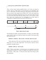
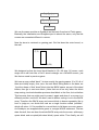
A standard VGA monitor can be separated into rows and columns.It typically
contains 480 rows,with 640 pixels per row.The coordinate value number is
start from top-left-hand corner to bottom-right-hand corner,as shown in Figure
VGA Monitor. And Each pixel can display various colors,depending on the
state of the red,green and blue signals.
Fig 1
Each VGA monitor has its internal clock that determines when each pixel is
updated.This clock operates at the VGA-spcefied frequency of 25.175
MHz.The VGA monitor refreshes the screen in a prescribed mechanism which
is controlled by the horizontal synchronization , vertical synchronization , Red
signal , Green signal , and Blue singal.
The VGA monitor starts each refresh action by updating pixel in the
top-left-hand corner of the screen,which can be treated as the origin point of an
X-Y plan(0,0)(also see Figure VGA Monitor).After the first pixel is refreshed,the
VGA monitor refreshes the remaining pixels in this row.When the monitor
receives a pulse on the horizontal synchronization , it refreshes the next row of
pixels.This process is repeated until the VGA monitor reaches the bottom of
the screen.When the VGA monitor reaches the bottom of the screen, it
receives the vertical synchronization pulses, causing the VGA monitor to begin
refreshing pixel at the top-left-hand corner of the screen.This is the operation
of the VGA monitor Updating Mechanism.
2.2 The Altera UP1 board VGA interface:
The Altera FLEX 10K-EPF10K20RC240-4 device has VGA 15 –pin D-Sub port
to connect the CRT (Cathod Ray Tube) monitor or LCD(Liquid Crystal Display)
monitor.Certainly , the UP1 board has internal diode-resistor network to handle
on the VGA protocol.The 15-pin D-Sub connector port with the diode-resistor
network are designed to generate signals that conform to the VGA standard.
Information about the color of the screen, and the row and column indexing of
the screen, are sent from the Red,Green,Blue signals of UP1
EPF10K20RC240-4 device. The other two signals are to control the horizontal
and vertical synchronization.This five signals allows images to be displayed to
the VGA monitor.
The 15-pin D-sub VGA connector consist of 15 pins including ground, red,
green, blue, horizontal synchronization, vertical synchronization and the other
pins are no connect.All of the lines are directional from the UP1
EPF10K20RC240-4 device (In this project, this device is to simultate a
computer system) to VGA monitor. Table D-Sub coneection lists the Pin
information of D-sub connector and the EPF10K20RC240-4 device.
Fig 2
2.3 VGA Timing:
For the VGA monitor to work ,it must receive data at specific time with specific
pulses.Both horizontal synchronization pulses and vertical synchronization
pulses must occur at specified times to synchronize the monitor while it is
receiving color data.The figures Horizontal Refresh Cycle and Vertical Refresh
Cycle show the timing waveforms for the color information with respect to the
horizontal synchronization signal and the vertical synchronization signal.
Fig 3
The frequency of operation and the number of pixels that the monitor must
update determines the time required to refresh each pixel, and the time
required to update the whole screen. The following equations calculate roughly
the time required for the monitor to perform all of its functions.(refer to UP1
board user manual)
(Notice:The UP1 board user manual use the wrong unit in the vertical part.)
Tpixel = 1 / fclk = 40 ns
Trow = A
= ( Tpixel * 640 pixels) / ( row + guard bands)
= 25 us + B + C + E
=31.77 us
TScreen = ( Trow * 480 rows ) + guard bands
= 15.5 ms + P + Q + S
= 16.6 ms
fRR = 1 / TROW = 31.5 kHz
fSR = 1 / TSCREEN = 60 Hz
Where Tpixel = Time require to update a pixel
fclk = 25.175 MHz
TROW = Time required to update one row
Tscreen = Time required to update the screen
fRR = Row Refresh frequency
fSR = Screen refresh frequency
The VGA monitor writes data to the screen by sending red, green,
blue ,horizontal synchronization, vertical synchronization signals when the
screen is at the expected location. Once the timing of the horizontal
synchronization signal and vertical synchronization signal is accurate, the VGA
monitor only need to keep track of the current location, so it can send the
correct color data to the pixel.
2.4 VGA Operation:
The VGA signals that are red, green, blue is sent from UP1
EPF10K20RC240-4 device to the VGA monitor amongst the pulses of the
horizontal synchronization signal and the vertical synchronization signal. At
beginning , the horizontal sychronization signal and the vertical sychronization
signal are high. If we want to show pixels in the screen, we have to send the
red, green, blue data of the first row and wait 0.94 us(Rear Guard) then we
send low of horizontal synchronization signal for 3.77us and wait 1.89us(Front
Guard) as the horizontal sychronization is high again.When we finish the first
row, we can send the second, third and the other rows in the screen by the
same way. While we send all of rows in the screen, we have to wait 0.35
ms(Rear guard) afterward vertical synchronization signal can be low for 64 us
and wait 1.02ms(Front Guard) as the vertical synchronization signal is high
again. Notice that whether the vertical synchronization signal is high or low, the
horizontal synchronization is still to send its singal to the VGA monitor, and the
RGB data keep low. The operation follows the step below:
1. The horizontal synchronization signal and vertical sychronization signal are
high.
2. Sending the RGB data in a row by RGB lines to the VGA monitor.
3. The RGB signal should be low and wait 0.94 us(Horizontal Front Guard).
4. The horizontal synchronization signal changes to low for 3.77 us.
5. The horizontal synchronization signal changes to high for 1.89 us and at this
moment, the RGB signals should be low(Horizontal Rear Guard).
6. Repeat step 1-5 to send the remaining rows until all of the rows in screen
have sent.
7. Repeat step 1-6 for 11 times. It is equal to wait for 0.35 ms(Vertical Rear
Guard).
8. The vertical synchronization signal becomes low for 64 us; It is equal to
repeat step 1-6 to for two times. Then the vertical synchronization signal
becomes to high.
9. Repeat step 1-6 for 32 times.It is equal to wait for 1.02 ms(Vertical Front
Guard).Then go to step 2 for refreshing new screen data.The whole process
is over.
Actually, if we compare these step with figure Horizontal Refresh Cycle and
figure Vertical Refresh Cycle then we can understand easily and know which
step mapped with the A,B,C,D,E,P,Q,R, and S. We will discuss how many
pulses we need in each step and we will use these letters for indicating each
step.
Horizontal Timing:
Horizontal Blank
B:
3.77 us
Front Guard
C:
1.89 us
Horizontal Columns
D:
25.17us
Rear Guard
E:
0.94 us
A=3.77us + 1.89us + 25.17us + 0.94us =31.77us
Vertical Timing:
Vertical Blank
P:
64 us
Front Guard
Q:
1.02 ms
Vertical Row
R:
15.25ms
Rear Guard
S:
0.35 ms
O=64us + 1.02ms + 15.25ms + 0.35ms=16.6ms
2.5 Memory Mapping versus Calculation:
We can roughly divide the VGA display methods into two types. One is
memory mapping, the other one is use circuit to calculate what color should be
shown in where of the screen. The idea of memory mapping is very simple, it is
just to keep the pixel of the VGA monitor correspond to memory. Just image
that each pixel of the VGA monitor refers to memory data, when the device
wants to send data to the VGA monitor , it only needs to check what color data
is stored in the corresponding memory address.
This method is one pixel (or block) refers to one memory address.
The other method, use circuit to calculate what color is be shown in the right
address.This method will not use the memory component, it uses logic circuit
to control what shape and where it is displayed on the screen.
We can image it works in the real-time environment, and it can be
implemented by registers and logic circuit.
In our project, we use memory mapping method, and the memory component
what we use is alter’s lpm_ram on the UP1 board.
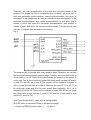
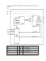
2.6 VGA Implement:VGA Synchronization:
We have discussed what time the horizontal synchronization sigal and vertical
synchronization signal should be high and low, and the clock and counter can
make us know what time it is while we send data to the VGA monitor.
Therefore, we must compute each of the time and find their number of the
pulses.In our project, we use a component which is called “vga_sync.vhd” to
deal with horizontal synchronization, vertical synchronization, and when to
send data. In this component, we use two counter to record the postion of the
horizontal synchronization and vertical synchronization in time axis. One in
named H_count that count the horizontal synchronization, and another is
named V_count that count the vertical synchronization. This two counter can
also use to evaluate the coordinate of the screen.
Fig 4
The program will be worked after every positive edge. Therefore, we can add
the horizontal counter at every positive edge. Certainly, we know every pulse is
40 ns (Actully, it is 39.722ns) so we can evaluate the number of the pulses in
every step. The H_Count must be added 640 times (each row has 640 pixels)
in step 2 or we can’t go to step 3. The counter will be needed to increase to
659 in 3 step, then we can go to step 4. Because we have 26.11 us (25.17 us
for horizontal pixels and 0.94 for rear guard) from beginning, 26.11 us is
divided by 40 ns (or 39.722ns) and the answer is nearly 659. So we can know
the 4 step need to wait until the H_count is 755. And the 5 step needs to wait
until the H_count is 799.
This Figure Shows that H_count and its’ timing relation
(B,C,D,E refer to Horizontal Timing in the previous page)
--<-Clock out RGB Pixel Row Data ->
<-H Sync->
---------------------------------------------______---------------________
--0
640 659
755
799
|**************D************|**E**|****B*****|**C****|
If H_count is 799, then set it zero and go to step 6. The program in the 6 step
we should increase V_count. The V_count in the program will inrease from 0 to
480(there are 480 rows on the screen) then go to step 7. Because the H_count
is still to add and the V_count is increased when H_count is 799. Therefore,
we can’t go to step 8 until V_count is 492. Because we have 15.59 ms (15.24
ms for rows and 0.35 ms for rear guard) from beginning, 15.59 ms is divided by
31.77 us (one horizontal over time) and the answer is 492. Therefore, we can
know the 8 step need to wait until the V_count is 494. This program finish to
draw a screen when V_count is 524, total time is 16.6 ms.
This Figure Shows that H_count and its’ timing relation
--<---- 480 Horizontal Syncs (pixel rows) --> ->V Sync<-------------------------------------------------_______------------- 0
480
493-494
524
|*************R************|**S***|**P***|***Q***|
2.7 VGA Implement:Memory Mapping
Because we use memory mapping in this project, so we must handle on the
memory. The Altera Maxplus provides the lpm_ram , we use this component to
save the data of the screen. But the UP1 board’s memory capability is not
enough to save all pixels of the screen, so we divide the screen into many
blocks, each block is 16 pixels * 16 pixels. In the memory , the data of color
uses 3 bits to record the red, green , and blue of each block, and use 11 bits to
save address of the block on the screen.
Because each block is 16*16, so the lower 4 bits (4 bits can indicate to 16)of
the horizontal counter (H_count) and vertical counter (V_count) we don’t use,
so we don’t care it. The lower 6 bits of this 11 bits address data is horizontal
part, and the high 5 bits of address data is vertical part. The horizontal part is
from H_count ( 10 bits) ‘s higher 6 bits., because the H_count ‘s range is from
0 to 799 so we must use 10 bits (0 ~ 1024) to save it. Each row has 640 pixels
(640 > 512) , so we must contain the highest bit and minus lower 4 bits (block
size).The vertical part is from V_count (10 bits)’s ninth bit to fifth bit, because
the V_count’s range is from 0 to 524 so we must use 10 bits (0 ~ 1024) to save
it. There are 480 rows (512 > 480) on the screen, so we need not to contain
the highest bit , just from ninth bit to fifth bit can show the block address of the
vertical part.
This figure is H_count and V_count address save in ram with abstract
coordinate.
Fig 5
This figure shows the coordinate when display on screen.The grid part is
not show on the VGA monitor.
Fig 6
This figure is the vga ram component.
Fig 7
There is one signal to do the enable of ram, when this signal is 1, we can write
data to the lpm_ram, when it is 0, the lpm_ram sends the data out. The
lpm_ram’s frequency synchronizes with UP1 board, so we can direct use the
global clock of UP1 board. The lpm_ram sends red, green, blue data to vga
synchronization part, because this two part (lpm_ram and vga synchronization)
work at the same frequency, so we can determine the coordinate of the screen
just by H_count and V_count. When V_Count is 481 (Rear guard), we assert
the write_enable to high for 1 H_count time, then we deassert it to low. During
this time, lpm_ram can receive data of color and address from other
component, in other time, lpm_ram does it job to send red, green, blue data to
VGA synchronization part.
In our project, we call this lpm_ram to vga_ram to identify the ram component.
Because we set a period time to access the vga_ram, so we must have a
control circuit to determine when the vga_ram should receive or send data.
And this control circuit should receive H_count and V_count from VGA
synchronization part to evaluate time, and receive data from Excalibur board.
Besides, we can load mif file to the lpm_ram, but in our project we use Nios on
Excalibur board to calculate the data and send it to the lpm_ram on UP1 board,
so we don’t use mif file.
The figure shows that the combination of VGA synchronization, VGA_ram, and
control unit.
Fig 8
Signal
I/O
Length Comment
reset
In
1 bit
Reset the screen
clock
In
1 bit
25.175 MHz clock
Clear
In
1 bit
Clear memory data
W0
In
14 bits Receive Data line 1
W1
In
14 bits Receive data line 2
Write_enable
1 bit
VGA_Ram enable signal
Write_dat
3 bits
VGA_Ram receivable data lines
Ram_address
11 bits Select ram address to save data
Red
Out 1 bit
The red signal
Green
Out 1 bit
The green signal
Blue
Out 1 bit
The blue signal
Horiz_sync
Out 1 bit
Horizontal Synchronization
Vert_sync
Out 1 bit
Vertical Synchronization
3 PS/2 Keyboard:
There is one PS/2 interface port on the Altera UP1 board. We can use
it to connect a mouse or a keyboard. The PS/2 port consist of 6 pins
including ground, VCC, keyboard data, and a keyboard clock line.Two
of the lines are not used. Both the clock and data lines are
bi-directional. The clock line is controlled by the keyboard, but it
is also manipulated by the processor or computer system when it sends
data. The data line is the only source for the communications between
the computer and keyboard.
Fig 9
The table is shown that the connection between pins of the EP10K240-4
FPGA on the UP1 board and the pins of PS/2.
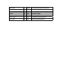
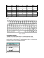
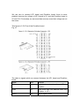
3.1 Keyboard Scan Code:
Data is passed serially to the computer from the keyboard using what
is known as scan code. Each keyboard key has unique code to identify
the key pressed.
3.2 Make and Break code:
The keyboard scan code can be divided into make code and break code.
The make code is sent every time a key is pressed. Once released, a
break code is sent. For most keys, the break code is a data stream
of F0 followed by the scan code for the the key. However, make and
break code may not be only one when it sends data.
The follow table shows the make and code.
Key
Make Code Break Code Key
Make Code Break Code
1
0E
F0 0E
31
1C
F0 1C
2
16
F0 16
32
1B
F0 1B
3
1E
F0 1E
33
23
F0 23
4
26
F0 26
34
2B
F0 2B
5
25
F0 25
35
34
F0 34
6
2E
F0 2E
36
33
F0 33
7
36
F0 36
37
3B
F0 3B
8
3D
F0 3D
38
42
F0 42
9
3E
F0 3E
39
4B
F0 4B
10
46
F0 46
40
4C
F0 4C
11
45
F0 45
41
52
F0 52
12
4E
F0 4E
43
5A
F0 5A
13
55
F0 55
44
12
F0 12
15
66
F0 66
46
1A
F0 1A
16
0D
F0 0D
47
22
F0 22
17
15
F0 15
48
21
F0 21
18
1D
F0 1D
49
2A
F0 2A
19
24
F0 24
50
32
F0 32
20
2D
F0 2D
51
31
F0 31
21
2C
F0 2C
52
3A
F0 3A
22
35
F0 35
53
41
F0 41
23
3C
F0 3C
54
49
F0 49
24
43
F0 43
55
4A
F0 4A
25
44
F0 44
57
59
F0 59
26
4D
F0 4D
58
14
F0 14
27
54
F0 54
60
11
F0 11
28
5B
F0 5B
61
29
F0 29
29
5D
F0 5D
62
E0 11
E0 F0 11
30
58
F0 58
64
E0 14
E0 F0 14
90
77
F0 77
110
76
F0 76
91
6C
F0 6C
112
05
F0 05
92
6B
F0 6B
113
06
F0 06
93
69
F0 69
114
04
F0 04
96
75
F0 75
115
0C
F0 0C
97
73
F0 73
116
03
F0 03
98
72
F0 72
117
0B
F0 0B
99
70
F0 70
118
83
F0 83
100
7C
F0 7C
119
0A
F0 0A
101
7D
F0 7D
120
01
F0 01
102
74
F0 74
121
09
F0 09
103
7A
F0 7A
122
78
F0 78
104
71
F0 71
123
07
F0 07
105
7B
F0 7B
125
7E
F0 7E
106
79
F0 79
The figure shows the position of key is mapped.
Fig 10
3.3 Keyboard Operation:
The scan code are sent serially on the bi-directional data line. When
neither the keyboard nor the computer want to send data, the data line
and the clock are high (inactive). The transmission data of a single key or
command consists of the following components:
BIT FUNCTION
11
Stop bit (always 1)
10
Party Bit (odd partly)
9
Data Bit 7
(most-significant)
8
Data Bit 6
7
Data Bit 5
6
Data Bit 4
5
Data Bit 3
(most-significant)
4
Data Bit 2
3
Data Bit 1
2
Data Bit 0
(least-significant)
1
Start Bit (always 0)
The following describes the typical sequence of events when the system is
receiving data from the keyboard.
1. The keyboard checks the 'clock' line. If the line is inactive(high), output from
the device is not allowed.
2. The keyboard checks the 'data' line. If the line is inactive, the controller
receives data from the system.
2. The keyboard checks the 'clock' line during the transmission at intervals not
exceeding 100 microseconds. If the device finds the system holding the
'clock' line inactive, the transmission is terminated. The system can
terminate transmission anytime during the first 10 clock cycles.
3. A final check for terminated transmission is performed at least 5 ms after the
10th clock.
5. The system can hold the 'clock' signal inactive to inhibit the next
transmission.
6. The system can set the 'data' line inactive if it has a byte to transmit to the
device. The 'data' line is set inactive when the start bit (always 0) is placed on
the 'data' line.
7. The system raises the 'clock' line to allow the next transmission.
The figure is timings for data received from the keyboard.
Fig 11
TIMING
PARAMETER
Min/Max
Time from DATA
T1 transition to falling 5/25 us
edge of CLK
Time from rising
T2 edge of CLK to
DATA transition
T3
T4
5/T4 - 5
us
Duration of CLK
30/50
inactive
us
Duration of CLK
30/50
active
us
Time to auxiliary
device inhibit after
clock 11 to ensure
T5 the auxiliary device
does not start
>0/50
us
another
transmission
The computer system can also send commands to the keyboard, These
include:
1. Keyboard initialization data.
2. Request for resend data of last time.
3. Illumination of status lights includeing CAPS-LOCK, SCROLL-LOCK, and
incNUM-LOCK LEDs
The following describes the typical sequence of events when the system is
sending data from the keyboard.
1. The system checks for a keyboard transmission in process. If a transmission
is in process and beyond the 10th clock, the system must receive the data.
2. The keyboard checks the 'clock' line. If the line is inactive, an I/O operation
is not allowed.
3. The keyboard checks the 'data' line. If the line is inactive, the system has
data to transmit. The 'data' line is set inactive when the start bit (always 0) is
placed on the 'data' line.
4. The keyboard sets the 'clock' line inactive. The system then places the first
bit on the 'data' line. Each time the keyboard sets the 'clock' line inactive, the
system places the next bit on the 'data' line until all bits are transmitted.
5. The keyboard samples the 'data' line for each bit while the 'clock' line is
active. Data must be stable within 1 microsecond after the rising edge of the
'clock' line.
6. The keyboard checks for a positive-level stop bit after the 10th clock. If the
'data' line is inactive, the keyboard continues to clock until the 'data' line
becomes active. Then it clocks the line-control bit and , at the next opportunity,
sends a Resend command to the system.
7. The keyboard pulls the 'data' line inactive, producing the line-control bit.
8. The system can pull the 'clock' line inactive, inhibiting the keyboard.
The figure is timings for data sent to the keyboard.
Fig 12
TIMING
PARAMETER
T7
T8
Min/Max
Duration of CLK
30/50
inactive
us
Duration of CLK
30/50
active
us
Time from inactive
to active CLK
T9
transition, used to
30/50
time when the
us
auxiliary device
samples DATA
T4
Duration of CLK
30/50
inactive
us
Time to auxiliary
device inhibit after
clock 11 to ensure
T5 the auxiliary device
does not start
another
transmission
But when we use the Altera UP1 board to connect keyboard, our data lines
zare unidirectional. Therefore, our project don’t implement the method of
computer sends data to keyboard.
3.4 Filter keyboard clock:
Because of the system clock is not the same as the keyboard clock. So we
must constructure a clock filter to make sure that there is keyboard’s data on
the clock block. In VHDL code, there is a 8 bits shift register to record the clock
data serially. When it records the keyboard clock by shift the data, we’ll check if
all of the bits of the register are 1, then the filter clock is high else the filter
clock is low. When the clock filter is high, we can get scan code.
3.5 Get scan code:
W can use positive edge of the filter clock to get the scan code. We must have
a counter to record which bit it is. And we must have to determine the start bit.
When we get the first data, we set the read_char to 1 and use this signal to
start get keyboard data serially. All of the scan code are 8 bits, so we set a
counter to count time and use a 8 bits shift register to record the data. When
the counter is 9, we send the scan code out and clear the counter and the
read_char signal for next scan code.
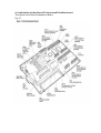
4. Combination of the Altera UP1 board and Excalibur board:
This figure is the Nios Development Board.
Fig 13
We use wire to connect UP1 board and Excalibur board, there is some
problem because the voltage of UP1 board is 5V, and the Excalibur board is
5V and 3.3V. Fortunately, we can send data correctly even their voltage are not
the same.
This figure is 3.3V Pins of the Excalibur board.
Fig 14
The table is signals which we connect between the UP1 board and Excalibur
board.
Signal
Bits
Commet
Action
3
Send keyboard action from UP1 to
Excalibur
Head
14
Send RGB data and address data from
Excalibur to UP1.
Body1
14
As the signal “Head”
Body2
14
As the signal “Head”
Tail
14
As the signal “Head”
Clear
1
This signal from Excalibur to UP1 to clear
the ram data.
Sel
1
This signal from Excalibur to UP1 to
select what type of keyboard style we
want to use.
4.1 What is Nios??
Nios is a 32 bits embedded processor, we can design this system module by
using SOPC builder and Quartus. Then we download it into the Nios
development board. With SOPC builder, we can connect the Nios system
module to the interface with RAM, flash memory, LEDs, LCD, switches,
buttons and others.
4.2 Use SOPC builder to make a Nios 32-bit CPU:
In this part, we follow the step of the pdf file “Nios_Tutorials_2_0.pdf” to make
a Nios CPU module. But we modify some part for our project.
Design Entry
1. Use Quartus to create a new project.
2. Create a BDF file.
3. Start SOPC Builder, and add CPU and peripherals.
4. Generate NIOS-32 and ADD It to the design.
5. Add the symbol to the BDF file.
6. Add pins and primitives.
7. Name the pins.
8. Make the final connection.
Compilation
1. Create compiler settings.
2. Assign signals to device pins.
3. Compile.
After compilation, the Quartus will create a file called “nios.h” , it is like header
file we use in C. Quartus defines the hardware data in this nios.h.
We can use it like we use header files in C language. Then we can use Nios
SDK shell to build it to “srec” file, and then we can run this “srec” file on the
Excalibur board.
Programming
1. Configure an APEX device.
2. Running Nios SDK shell.
The figure is using SOPC builder to build Nios and peripheral port.
Fig 15
This figure is using Nios SDK shell to build “srec file”.
Fig 16
Notice that when we use Nios SDK shell to run srec files, we use debug mode,
so we connect the Excalibur board to computer’s RS232 port. Then we use
Nios SDK shell to control Nios system module to do its job.
5. Some problems of hardware:
In order to improvement the performance of the game, we must solve some
problems. We can overcome them by software and hardware. This part is to
describe problems which we have encounted.
5.1 Increasement of VGA's block refresh rate:
When we start to use Nios to control the logic part of the game, we use one
channel (14 bits) to send RGB data (3bits) and address data (11 bits) to
memory. In this method, the Excalibur board send 1 block each time, but it is
too slow. So we increase 3 channel to send data, they are called “head”,
“body1”, “body2”, “tail” in our project.
Therefore, when we change the original 1 channel to 2 channels, the refresh
rate of the block is more faster. But when we increase to 4 channels, the
advancement of the refresh rate is not as good as 1 channel to 2 channels.
5.2 To clear the VGA blocks:
If we use software to fill all the VGA block to black, its looks like we clear the
monitor. But it is too slow, so we use a wire we called “clear” to do this job. This
signal is from the Excalibur board to the UP1 board. When the clear signal is
high, the UP1 board’s VHDL component fill all the vga_ram address with black
(RGB data is 000).
We use this method to make sure that we can clear the VGA monitor without
delay.
5.3 Keyboard contiunes sending the same scan code until the other key
is pressed:
We use a VHDL component to do a keyboard decoder. When the we pressed
“up”, “down”, “left”, “right”, “Enter” or“ESC”, this component decode them to
different data and send them to the Excalibur board. When we pressed the
other key, this component don’t pay attention to them, including the break code
“F0”.
Software Aspect
So far, we ‘ve designed literally a VGA system . What indeed is better to test a
nd validate a video system than some familiar video games ? And by the
powers of Quantus, despite some minor difference on I/O routines, we are
practically able to implement our small games in C++ languages. Now that is a
good news indeed.
Overview
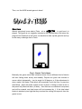
Thus, our first video game is a old game called “Snakebyte”, a.k.a. “貪食蛇”,
which is now very popular among most cellphones. In case that you haven’t
played this game, tts process screen is just like below :
Fig s1, Snakebyte concept.
As we can see, a hungery large snake trying to eat an apple. Everytime it gets
an apple, it grows larger, thus making the movement more difficult, since the
snake cannot bite itself or bump into the wall, otherwise the game ends.
Of course, our game won’t be as detailed as the picture shown above, since
the video system we designed can only held its resolution in 40 x 30 , and with
8 colors. Thus a minium pixel in our system equals to a 16x16 sized rectangle
on a 640x480 on PC. The snake will only appeared like a series of
not-so-small dots, each a size of 16 x 16 pixels in a normal 640x480 on a PC.
The wall will surround the whole screen bound, which makes it 40x30 “big”
pixels. And each apple will be an exact dot.
Data Structure
For convenience, I used a simple structure than contains two integers, which
is called “Crd”, abr of coord, which can be used to represent both the snake
segments and apples.
Typedef struct { int x,int y; } Crd;
Our snake , as shown above, is segmented, therefore can be treated as
separated dots. Using Crd structure defined above, the snake is defined like
this:
Crd snake[30];
Of course, the number of the snake’s segments varies dynamically. Our
thought is that we define another integer variable to record how long it is now,
and while dealing with snake, we only so care about those array blocks that
are smaller or equal to the snake length, thus compensating the stationary of
using array.
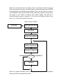
Flowchart
Now, lets talk something about implementation. The game itself can roughly
be divided into three parts : initalization, the gaming part, and end game :
Initalization
Game in process
End game
Fig s2.
On PC with Turbo C++, INITALIZATION means switching to graphic mode by
invoking BGI drivers. In our case on Nios, some I/O settings have to be done
before we can really draw anything on the screen and receiving messages
from the keyboard. We will then process to giving all the variables that require
initial values. For example, function “init_snake” gives the blocks in “snake”
array all the beginning values, which decides where the snake will appear the
the game is booted. And maybe we would like to show a title screen, some
fanfare to our hard work.( though with the poor resolution we get it don’t looks
that good anyway. ☺ )
Initalization
NIOS I/O settings.
Initial values assign.
Show title screen.
The gaming part, which I embedded into the MAIN function itself, is the
essence of this whole program. The game, is itself a WHILE statement. Until
the snake is dead, user win, or user quit the game manually which is
accomplished by pressing ESC key, the iteration goes on and on. Inside the
WHILE statement, we first have to draw the surrounding wall, which is
necessary only the first time, since its location on the screen is fixed , won’t
change, and won’t be covered by the snake unless it bumps into the wall,
which the game ends. Then we show the snake, show the current apple, then
we start reading the message from the keyboard, which is stored in integer
variable KEY. There is only so many possibilities : UP, DOWN, LEFT, RIGHT,
ESC, and ENTER. We use a switch to cover all these actions, and do the
respective actions like turn the direction of snake, start or quit the game. Then
we’ll have to check to see if the snake going this new direction (maybe it’s the
same with previous loop) will bump into a wall, get a fruit , or just going very
well. If it bumps, signal the game ends in DEAD. If it eats, and the total length
is not exceeding the winning standard, it length get a increment, else quit the
game and signal WIN. Else, (neither bump nor eat) just move the snake
according to the direction, then jump to next loop.
The gaming part flowchart is shown below:
Draw wall
Show snake
Show fruit.
Read keyboard message.
Respond to key stroke.
ESC
Arrow keys
Normal
Update new snake status
BUMP
Gets fruit
See if total length is long enough to win
Yes
Proceed to end game.
Increase length,
Generate new apple.
Move snake in new direction.
Then comes the endgame part. It clears the screen, show some endgame
screen of its own, and shows the total score the player earned.
Clear screen
Show end game screen
Show score
END
I/O issue
There is two I/O device involved in this video game. One is monitor, to which
we draw our gaming, thus an output device. The other is keyboard , from which
we get our message, thus an input device.
Of course, the detail of how to control these two devices are not the main
issue here. The UP1 board loaded with controlling VHDL codes ‘ll take care of
everything. Here we merely have to use them through the I/O channels defined
in NIOS.H, header file generated by Quartus II.
Before sending or reading anything from a channel, we first have to specify
wheather this channel is for INPUT or OUTPUT.
void initgraph(void)
{
na_key_pio->np_piodirection=0; //specific input
na_head_pio->np_piodirection=3; //specific output
na_body1_pio->np_piodirection=3; //specific output
na_body2_pio->np_piodirection=3; //specific output
na_tail_pio->np_piodirection=3; //specific output
}
There is three output channel specified above, all of them are going for
monitor., each as a “data window”. We put the data to the window(pin), then
once in a little while, the VHDL codes at the other side will come and “pick”
them up, decode, then update them to RAM on UP1. Since one window can
only held one pixel before being picked up by UP1, we cannot output too quick
ly or else some data will be lost, thus causing “holes” on the screen. In other
word, each entry outputed must be accompanied by a short delay to
compensate the frequency difference between NIOS and UP1.
Nios output delay Nios output
16ms
delay
16ms
Nios output
delay
16ms
VHDL pickups
Fig s4, single channel output.
The best delay time above, by experiementation, is roughly 16 ms each single
output, which is really not so short an interval if we want to fill the screen with
dots, which will cost :
40x30x16 = 14400ms = 144 seconds = 2 minutes and 24 seconds
That’s really slow !! But now, by add three channels, we can shorten the
delay time to 2 ms for each output action. Thus the time it takes to clear a
screen(fill it with black dots) is :
40x30x2 = 2400 ms, = 24 seconds.
WOW !! That’s much better !! ( We did scream in the laboratory when this
improvement is carried out ) Though in the game we actually use a much more
rapid method , VHDL codes , to clear the screen rather than having to paint
each dots black.
To switch active channels back and forth, we declared a integer flag to show
which one is to be written next, then write to it. Once the output is done, we
delay 2 ms, then change the flag to another channel for the next output action.
int flag=0;
void put_pixel(int x,int y,int color)
{
switch (flag) {
case 0:
na_head_pio->np_piodata=x+(y<<6)+color;
flag++; break;
case 1:
na_body1_pio->np_piodata=x+(y<<6)+color;
flag++; break;
case 2:
na_body2_pio->np_piodata=x+(y<<6)+color;
flag++; break;
case 3:
na_tail_pio->np_piodata=x+(y<<6)+color;
flag=0;
}
nr_delay(2); }
To invoke the hardware clearscreen function, we need only to specify below:
void clearscreen(void)
{
na_clear_pio->np_piodirection=1;
na_clear_pio->np_piodata=1;
nr_delay(16);
na_clear_pio->np_piodata=0;
}
// signal direction.
// Enable function
// wait UP1 to pick up the signal
// Disable function
As for input device , keyboard, since we have already set its channel to input,
now we merely have to get signal from it.
int key;
void readkey()
{
key=na_key_pio->np_piodata;
}
Therefore once we invoke readkey(), it will read the lastest pressed
recongizable key number from na_key_pio and store it in the variable KEY.
*Snakebyte implementation.
Now that we have all the tools we needed we can combine them with the
mid-leveled flowchart designed above, using these I/O functions to complete
the low level functions.
Initsnake( ) – This function sets the initial values of the snake by a simple FOR
loop.
Show_wall( ) – two FOR loop to draw a 40x30, 1-dot-deep rectangle on the
screen;
Show_snake( ) – In fact, this function only shows the head of the snake, which
is Snake[0]. Before doing so it first clear the last tail of that
snake, thus creating an illusion of a whole snake moving.
Show_fruit( ) – Prints the fruit on the screen according to its coord;
Next_snake( ) – this function first do below :
Snake[n] = snake[n-1]
Snake[n-1] = snake [n-2]
…
Snake[1] = snake[0]
,transfering each snake segments to next.
Then , according to current direction(another variable),
It updates snake[0] to a new coord.
Switch(direction)
{ case U: snake[0].y--; break;
case D: snake[0].y++; break;
case L: snake[0].x--; break;
case R: snake[0].x++; break;
}
So now the snake is in its next position.
Is_dead( ) – This function checks to see if snake[0] ‘s value is equal to the
coords of the wall , or equal to anyother segments of itself. That
is , if the snake bumps into a wall , or bite into itself. If any above
condition, then return 1. Else, it proceed to see that is snake[0] is
equal to the coord of the apple. If yes, then increase the length of
snake by 1, then generate a new apple.
Gameover( ) – Show the endgame screen as well as the total score(length) the
player has earned.
Title( ) – Show the introduction screen.
So the main function is roughly like this:
int main(void)
{
int a,b,dir=13;
char d='r';
long i,delay,k,start=0;
int location_y,location_x,l;
initgraph();
selftest();
printf("\n\n\n");
printf("Hello, from Nios!\n");
printf("Please observe the Nios board...\n");
initsnake();
show_snake();
show_wall();
do
{
show_snake_head();
show_fruit();
readkey();
if(key==5 && start==0)
{
start=1;
printf("Start moving!");
}
put_pixel(snake[top].x,snake[top].y,BLACK);
nextsnake();
if(key==0){
if(d!='d') d='u';
}
else if(key==1){
if(d!='u') d='d;
}
else if(key==2)
{
if(d!='r')d='l';
}
else {
if(d!='l') d='r';}
switch(d)
{
case 'u' : snake[0].y--; break;
case 'd' : snake[0].y++; break;
case 'l' : snake[0].x--; break;
case 'r' : snake[0].x++; break;
}
if(is_dead()) { printf("is_dead()==1)"); break; }
nr_delay(dir);
}while(key!=4);
clearscreen();
gameover();
printf("Good bye.\n\004");
}
Thus, our first NIOS arcade game is done!
Overview
Almost everybody know what a Tetris , a.k.a. “俄羅斯方塊” , is, and how it is
played. This game is not originally intended to be included here. But since the
progress on Snakbyte is well done, we decided to take up this gauntlet and up
to the many challenge that is Tetris.
Fig t1, Classic Tetris Game.
Basically, the game starts with a blanket sheet. Seven different kind of blocks
will then falling down slowly and steadily. Players are given the choices to
move a block horizantally , turn its angel for 90 degree, or if the adjustment is
done, make it fall faster. Each block will eventually touch the floor, or previous
dead block , which will make it dead, frozen in place. If doing so make a row in
the panel fully filled with dots (10 dots) , then that row is considered conquered,
and will be erased, and total score will be increased by 1. If the total dead
blocks is stacked up so high that they touched the celling of the panel, then the
game is over.
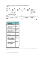
Data structure
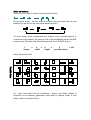
First of all, we ‘ll have to draw all seven kinds of blocks.
By using 4x4 arrays , we can cover all of them very accurately. But the real
problem is, how can we flip each block back and forth ?
To avoid doing some complicated and fruitless array caculation(which is
unique with every shape), we simply put all of the possibilities into the SHAPE
array as well. Therefore, the size and dimension of our SHAPE array is :
7
shapes
x
4
x
width
4
x
height
4
= 238
possible status
which will look like this:
Fig t3. Shape table.
So , each new block has two information : shape, and status. Shape is
supposed to be randomly generated, while status is always initally 0 until
player makes command to flip it.
Initalization
Game in process
End game
We use the same module as Snakbyte as the basic flowchart of Tetris game.
Basically, the Initalization and Endgame part is almost the same, only the title
screen are somewhat different in names.
Now the issue is centered on gaming part. We first draw the outer bound, or
the wall.
(7,3)
(18,24)
screen
We designed so that the inner block blanket is 10 x 20 dots. Of course, each
single dot is still look like a 16x16 sized rectangle on a 640x480 screen, just
like that we used in previous game.
We have a array called “back”, its size exactly the gaming space 10 x 20, all of
them are initally empty, thus, zero. As each block falling down to the base, we
‘ll put the shape of that “dead” block into the BACK space, as part of the dead
blocks, then go to next new block. (Note that we do so only when the block
stop moving, touched wheather previous dead block or the floor, but not before.
This because that we might need to erase it again and draw it on screen in a
different position next time. We don’t want to bother sorting it out in the BACK
array. Therefore the BACK array and current block is drawn separately) As to
how to judge so, we divide this task as a single function called “possible”,
which will return 1 if it’s possible for current block to fall down one more space.
As Snakbyte, we wrapped whole game in a single WHILE statement. First we
draw the wall, then we draw the whole BACK array onto the screen, with empty
space black and occupied(with dead block) space white. Then finally, we will
draw the current block onto the screen. Then, we will see if there is any key
stroke, and respond to them. (Left and Right for horizantal adjustment, ENTER
for flip 90 degree and DOWN for going down) Then, we will check a counter to
see wheather in this loop the block will be “affected by gravity” and go down
one space or not. There is another value called “speed”. We will see if
(counter%speed equals) to (speed-1). If yes, then we signal the block to go
down. If no, then we proceed to next loop.
Main function of Tetris.
Draw wall
Generate New Block
Draw Back
Draw Current Block
Counter increase by 1
Respond to Keyboard
(counter%speed) equals to (speed-1)?
Yes
GoDown
Above is a simple flowchart of our main program. Many details are wrapped
inside and will be expanded fully below.
First is the box of “Respond to keyboard”.
Readkey( );
switch(key)
{
case DOWN :GoDown(x,y,CurrentShape,Status);break;
case LEFT :GoLeft(x,y,CurrentShape,Status);break;
case RIGHT :GoRight(x,y,CurrentShape,Status);break;
case ENTER :ChageShape(x,y,CurrentShape,Status);break;
case ESC :end();
}
Among them, function GoLeft simply decreases the horizantal location of the
block while GoRight increases. Above two actions will only commence if that
block is not close the wall, thath is the value returned from function possible( )
is 1. ChangeShape will increase current shape status by 1, usless it’s already
3 ,in which case ,after executing ChangeShape, will be turn to 0 again. Again,
this function will first see to function possible( ) to decide wheather it will flip or
not.
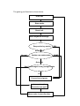
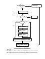
Function GoDown is far more complicated, for it has to deal with many
possibilities : normal going down with no other block below, touch-down,
touch-down and erase one or more row, and game over. Normal goind down
first check to see if going down is possible. If yes, then increase Y by 1. If no,
then proceed to touch down. When possible( ) return 0, the current block is to
be pasted into the BACK array, which makes it a dead block. After that, we ‘ll
see if this stack-up is too high(touching the celling). If it is, then invoke
Gameover( ). If not then, we proceed to check if there is any row being filled. If
there is, then we erase it(or them) from the BACK array, add up the score, then
update the screen with new BACK array. Then ,wheather any rows are erased
or not, we generate a new block, by involving CreateNewShape( ), then start it
all over again.
Possibility check
Location Y+1
Possible
Impossible
Paste shape of current block to BACK array
Is dead block too high ?
Game over
yes
NO
Check to see if any filled row
Yes
NO
Erase filled row
Add up score
Re-draw screen
Generate New Block with New Shape
Return to Main function.
Fig t4 Flowchrat of function GoDown( )
I/O issue
Basically, we use the same I/O functions as Snakbyte. Only now our keyboard
input driver is slightly different. In Snakbyte, the Readkey function returns the
last key pressed, wheather any key is currently being pressed or not. Now this
design is benefitical to Snakbyte, but not to Tetris. In Snakbyte, the snake is
always moving, even if we don’t press any key (except ESC, which quits the
game). In Tetris, we have to be very careful with the key we pressed. If we still
use the same keyboard driver as Snakbyte, then a single ENTER stroke will
make the block flipping continuously like a helicopter , for the Readkey( )
function keeps returning ENTER even if it’s no longer being pressed.
In the keyboard driver for Tetris, we added a new key number 7, that means
there is no key currently being pressed, thus solving the problem.
Afterword:
蔡祁名:
I think that our project name “Using SOPC builder to fast generate digital
prototype system” is very very metaphysical. I admire for our teacher because
he can make this great project name. Though Quartus is a very powerful
program, and SOPC builder is a very convenient to set Nios module’s I/O port
and other component. But the most of my job is to handle UP1’s I/O. Frankly,
we don’t cost much time on SOPC builder or Quartus.
I spent much time and energy on VGA part and keyboard part, both of this two
component are very skillful because they are changeful. In our project I add a
clear signal to VGA part and try to modify keyboard. Unfortunately, there is still
a bug on the keyboard part. At last time, I add a counter on Excalibur board,
but my partner doesn’t use it, so we don’t know how does it work.
As the teacher Wang said, can we put the VGA synchronization and control
unit with lpm ram on the Excalibur board? If we have a noiseless D-sub
channel to translate data, may be we can implement it without noise signal.
But……..the biggest problem is still “time”.
I think it is a pity that we have not enough time because our teacher change
our projects many times, so we only use two months to make all the project
done. If we have more time and more “care” from our teacher, we may make
this project more better.
陳光和:
So we did it, such a accomplishment. We really don't sure ( or know) what we
are doing until the last two months, which the hardware is 60% completed and
can accept C code. Thus I started to transplant those programs I have finished
on 80x86 with Turbo C ++ to NIOS C. The basic program(game) structure /
flow char didn't change much, only those of lower level I/O has to be
re-programmed(For example, function PUT_PIXEL, which outputs a pixel to
the given location of screen). Foreseeing this, I used modulizing concept while
programming them on PC, splitting the whole program into little pieces of
functions. Doing so decreased the overall performance since the switching
between functions and procedures took time and resource, but it's a small
friction that our hardware can afford to.
The real problem was that I programmed Tetris on a Pentium 450MHz, while
our NIOS CPU is only 25MHz. Thus when the transplant completed, the
performance was very poor. I had to do some modification (or "diet" )on the
program, extract as much resource as I can , while reducing the numbers of
output as possible. We developed the hardware Clearscreen function and
widened our data path to 4 channels. It was quite a advancement, quite an
improvement , with both software and hardware adjustment.
We originally intended to make the screen 640x480, then try to write a
role-playing game on it. Unfortunately, the hardware communication between
doesn't seem to be able to accept such high a frequency transfer. It's
suggested by the professor that if we move the hardware controlling codes
(VHDL) from the UP1 board to the NIOS board, which has almost 128K more
SRAM to use, thus greatly reducing the communications(thus wires) between
these two boards. If we have time and the determination in the future, maybe
we will do it.
Reference
1. http://www.networktechinc.com/ps2-prots.html
2. http://users.ece.gatech.edu/~hamblen/ALTERA/onedge/gatech/ps2keyboar
d.html
3. The Altera UP1 Manual.
4. The document of the Altera excalibur board.
5. http://www.ee.ualberta.ca/~elliott/ee552/studentAppNotes/
盧毅,賴杰,VHDL 與數位電路設計,文魁資訊股份有限公司,2002 年 2 月初版㆔刷