1
NC–930
V2
Isolated 24 Bit DIO Module
Rev: 1.0
Release date: 2013/07/25
1
Copyright
Copyright 2002 by NETCOM Co., Ltd. All rights reserved. No part of this publication
may be reproduced, stored in a retrieval system, or transmitted, in any form or by any
means, electronic, mechanical, photocopying, recording, or otherwise, without the prior
written permission of NETCOM Co., Ltd.
NETCOM Co., Ltd. believes to contribute accurate and conscientious information in
this manual. Nevertheless, no responsibility is assumed by NETCOM Co., Ltd. for its
use; nor for any infringements of patents or other right of third parties which may
result from its use. NETCOM Co., Ltd. reserves the right to change this document or
make improvements in the products described within at any time without notice.
IBM is a trademark of International Business Machines Corporation. MS-DOS,
MICROSOFT C and Quick BASIC are trademarks of Microsoft Corporation. TURBO
C is a trademark of Borland Inc. BASIC is a trademark of Dartmouth College. Intel is
a trademark of Intel Corporation
May, 2002
NETCOM Co., Ltd.
Printed in Taiwan
Edition Lili
2
CHECK LIST
Before getting started, check if your NC–930 Isolated 24 Bit DIO Module package
includes the following items:
NC–930 board
Screw 3mm (x 4)
Bronze stick 6mm (x 4)
NC–930 user’s manual
If anything is missing, please contact your dealer.
3
Table of Contents
CHAPTER 1 INTRODUCTION ......................................................................... 5
1.1 General Description .................................................................................. 5
1.2 Applications ................................................................................................ 5
1.3 Specifications ............................................................................................... 6
1.4 Accessories Guide 4……………………………………………………… 9
CHAPTER2 MODULE CONFIGURATION AND INSTALLATION……….9
2.1 Component Locator Diagram .................................................................... 9
2.2 Mechanical Information…………………………………………………..10
2.3 Base Address Switch.................................................................................... 11
2.4 IRQ Level Jumper ..................................................................................... 12
2.5 Isolated DI Port ........................................................................................... 13
2.6 Isolated DO Port.......................................................................................... 14
2.7 Hardware Description................................................................................. 15
2.8 Module Installation ..................................................................................... 15
CHAPTER 3 REGISTER STRUCTURE AND FORMAT............................... 16
3.1 I/O Address Map ......................................................................................... 16
3.2 Registers Description .................................................................................. 17
CHAPTER 4 PROGRAMMING......................................................................... 18
4.1 Digital Input and Output............................................................................ 18
4.2 Interrupt ..................................................................................................... 19
CHAPTER 5 APPLICATION ............................................................................ 24
5.1 Event Trigger ................................................................................. 24
APPENDIX A PC I/O PORT MAPPING............................................................ 27
APPENDIX B BLOCK DIAGRAM .................................................................... 28
APPENDIX C TECHNICAL REFERENCE...................................................... 29
General Usage of Digital Input and Output ................................................... 29
Port A, B and C Basic Definition ..................................................................... 31
APPENDIX D PC/104 MECHANICAL SPECIFICATION ............................. 32
PC/104 General Description............................................................................. 32
Module Dimensions ........................................................................................... 32
4
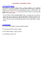
CHAPTER 1 INTRODUCTION
1.1 General Description
The NC-930 is a PC/104 module which is primary intended to PC embedded
application in industrial environment, containing Isolated 24-bit digital 16 input and
8output. It can used with TTL low-level input/output circuitry or with solid state relay
module such as NC-416 or NC-424 and provides 2500V isolation for interfacing with
high level AC and DC signals.
The 24 TTL/DTL/COMS compatible digital I/O lines are arranged into two separated
groups. Each group supports 8255 PPI (Programmable Peripheral Interface) chip
mode 0 but with stronger driving capability and consists of two 8-bit ports; Port A,
Port B. These ports can be functionally programmed as either digital inputs or digital
outputs.
1.2 Applications
Sense and control high level signals through I/O module
Sense low-level(TTL) switches or signals
Drive indicator light or control recorders
Parallel data transfer to PC
5
1.3 Specifications
INPUT AND OUTPUT
Input / Output Lines
Isolated Input16/ Output 8
Isolation up to 1000 Vrms
Operation Mode
8255 Mode 0
Input / Output Mode
Pair
Interrupt Options
Jumper-selectable to level
9(2),5,10,11,12 or 15
Improved Noise Margins
Hysteresis
VT+ - VT - =0.4typ.
Input / Output Level
TTL/DTL compatible
Added Pull-up Resistor
CMOS/dry contact compatible
Electrical Characteristics
VIH
VIL
IIH
IIL
VOH
VOL
IOH
IOL
2V min
0.8V max
20uA max. at VI=2.7V
–0.2mA max. at VIL=0.4V
2.4V min. at IOH=-3mA
0.4V max. at IOL=12mA
–15mA max.
24mA max
INTERFACE CHARACTERCTIC
I/O Cable Type
Ribbon Twisted Pair Cable
Ribbon Stripline Cable
Compatible Bus
Interface Type
Number of Locations occupied
Data Path
ZO = 50Ωto 100R typ
ZO = 30Ωto 80R typ
PC/104 bus
I/O mapped with 10-bit addressing
(A9 – 10)
8 consecutive addresses
8 bits
6
Power Requirements
+5V
0.4A typ
Physical/Environmental
Dimensions
95mm * 90mm
Weight
200g
Operating Temperature Rang
0 to 60℃
Storage Temperature Rang
–25 to85℃
Relative Humidity
To 90%, non-condensing
7
1.4 Accessories Guide 4
NC951
Screw terminal board for all digital I/O connections. Shipped with 3.3 feet (1 meter)
cable and 50-pin connector.
NC-954
24-channel opto-isolated D/I panel for signal connection and conditioning with the
NC-930. Shipped with 3.3 feet (1 meter) cable and 50-pin connector.
NC955
8-channel electromechanical single-pole, double-throw (SPDT) and 16-channel
opto-isolated digital I/P panel which is compatible with the NC-930 Shipped with 3.3
feet (1meter) cable and 50-pin connector.
NC956
24-channel electromechanical single-pole, double-throw (SPDT) which can be driven
by the NC-930. Shipped with 3.3 feet (1 meter) cable and 50-pin connector.
8
CHAPTER 2 MODULE CONFIGURATION AND INSTALLATION
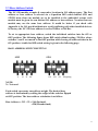
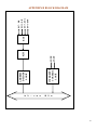
2.1 Component Locator Diagram
The following figure shows the location of NC-930’s components. All switch and
jumper settings in this figure are factory default setting.
9
2.2 Mechanical Information
10
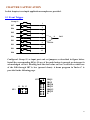
2.3 Base Address Switch
The NC-930 module occupies 8 consecutive locations in I/O address space. The first
address or base address is selected via a 8-position DIP switch labeled SW1 and
SW2.If more than one module are to be installed to the embedded system, each
module must be given its own distinct I/O address or base address. No more than one
module may use the same base address. It would be better if you check with
Appendix A for I/O port distribution to avoid conflicting with other installed devices.
In factory, the NC-930 base address is set for 220Hex or 544 Dec.
To set to appropriate base address, switch the individual switches into the ON or
OFF position. The following figure shows DIP switch default setting, 220 Hex, where
switches 1 and 5 are moved to the OFF position while leaving all other switches in the
ON position. A table for DIP switch setting is given in the following page.
BASE ADDRESS SWITCH SETTING
SW2
8
SW1
16
32
64
128
256
512
Weighting
NOTE:
X : Not used.
Each switch represents one address weight. The desired base
address is determined by adding the weight of the switches flipped
at OFF position. The base address calculation is as follow:
Base Address = 512 + 32 = 544 (Decimal)
=220 (Hexadecimal)
11
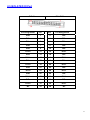
I/O PORT
RANGE
HEXADECIMAL
DIP SWITCH POSITION
200 – 207
1
A1
0
2
A2
0
3
A3
0
4
A4
0
5
A5
0
6
A6
0
7
A7
1
8
X
X
208 – 20F
1
0
0
0
0
0
1
X
210 – 217
0
1
0
0
0
0
1
X
218 – 21F
1
1
0
0
0
0
1
X
220 – 227 (*)
.
.
300 – 307
.
.
3F0 – 3F7
0
0
1
0
0
1
X
0
0
0
0
1
1
X
0
1
1
0
.
.
0
.
.
1
1
1
1
X
3F8 – 3FF
1
1
1
1
1
1
1
X
0 = ON,
1 = OFF,
(*): Factory Default Setting
X = don’t care
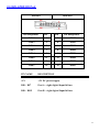
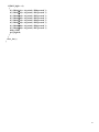
2.4 IRQ Level Jumper
Jumper labeled JP2 is used for selecting IRQ level (9(2),5, 10, 11, 12, 15). Below
figure gives the jumper configuration and default setting of JP2. Place jumper cap at
“x” position, if no interrupt is required.
JP2
1
13
IRQ9
IRQ5
IRQ10
IRQ11
IRQ12
IRQ15
X(NO connect)
12
2.5 ISOLATED DI Port
DIO-IN
DI0~DI15
Pin Assignment
Pin
Pin
Pin Assignment
DI0+
1
2
DI0-
DI8+
3
4
DI8-
DI1+
5
6
DI1-
DI9+
7
8
DI9-
DI2+
9
10
DI2-
DI10+
11
12
DI10-
DI3+
13
14
DI3-
DI11+
15
16
DI11-
DI4+
17
18
DI4-
DI12+
19
20
DI12-
DI5+
21
22
DI5-
DI13+
23
24
DI13-
DI6+
25
26
DI6-
DI14+
27
28
DI14-
DI7+
29
30
DI7-
DI15+
31
32
DI15-
NC
33
34
NC
13
2.6 ISOLATED DO Port
DIO-OUT
Pin Assignment
DO0~DO7
Pin
Pin
Pin Assignment
DOA0
1
2
DOB0
DOA1
3
4
DOB1
DOA2
5
6
DOB2
DOA3
7
8
DOB3
DOA4
9
10
DOB4
DOA5
11
12
DOB5
DOA6
13
14
DOB6
DOA7
15
16
DOB7
PIN NAME
DESCRIPTION
+5V
+5V PC power supply
DI0 – DI7
Port A – eight digital Input16 lines
DI8 – DI15
Port B – eight digital Input16 lines
14
2.7 Hardware Description
PC/104 module can be of two bus types, 8 bit and 16 bit. These correspond to the PC
and PC/AT buses, respectively. The detailed mechanical dimensions of these two
PC/104 bus types are provided in Appendix D.
Basically the NC-930 belongs to 16 bit bus option which is designed only to by pass
PC/AT bus signal in order to compatible to PC/AT type PC/104 module. The NC-930
uses only IRQ lines on P2 40-pin connector. If this module is going to plug onto PC
type PC/104 bus, do not use IRQ line above 10.
Beside bus option, there are stack through and non-stack through difference. The
stack through version provides a self-stacking PC bus. It can be placed any where in
a multi-module stack. The non-stack through version offers minimum thickness, by
omitting bus stack through pins. It must be positioned at one end of a stack.
For convenience, the NC-930 is equipped with stack through version only. (NOTE:
For safety, you are suggested to cut bus stack through pins of the last module on
condition; that you are sure you won’t add/plug any module to the module stack in
the future.)
2.8 Module Installation
The NC-930 board is shipped witch protective electrostatic cover. When unpacking,
touching the board electrostatically shielded packaging with the metal frame of your
computer to discharge the accumulated static electricity prior to touching the board.
Following description summarize the procedures for installing the NC-930.
WARNING
TURN OFF the PC and all accessories connected to the PC whenever installing or
removing any peripheral board including the NC-930 module.
Installation procedures:
1.
2.
3.
4.
5.
6.
7.
Turn off the system power.
Unplug all power cords.
Remove the case cover if necessary.
Remove the top module if it a non-stackthrough module.
Put the NC-930 module in line with the present module as described in Appendix D.
Install four spacers and fasten them if necessary.
Crush between the module until inside distance is SPACER’s height (0.6”). Restore
all the screws.
8. Repeat step 6 until all module are set into position.
9. Replace the case cover and connect all the necessary cables.
10. Turn on the system power.
15
CHAPTER 3 REGISTER STRUCTURE AND FORMAT
The NC-930 occupies 8 consecutive I/O addresses of PC/IO address space. During
installation, the first address or base address is determined by setting onboard DIP
switch (SW2 & SW1)
This chapter describes each NC-930 register in terms of function, address, bit structure
and bit function. Each register is easy to read and write to by using direct I/O
instruction of whatever application languages.
3.1 I/O Address MAP
The Isolated 24 digital I/O lines of NC-930 are arranged into two separated groups.
Each group supports 8255 PPI chip mode 0.
The NC-930 is programmable through configuration registers. By writing to control
register, the type of each group may be specified. If a group is configured as a write
port, the data drivers will drive the data value to the corresponding port. If a group
is configured as a read port, the data value on corresponding port will be sent to the
digital I/O lines.
The following table lists and describes the register and their locations (R = Read, W =
Write, Base = Base address).
Location
Function
Type
Base
Group #1 Port A
Group #1 Port B
Group #1 Port C
Group #1 Control Register
R/W
R/W
R/W
W
+0
+1
+3
+4
16
3.2
Register Description
Group #1 Data and Control Registers (Base + 0 to + 3)
Port A Data Register (Base +0, R/W)----- INPUT
base
+0
7
DI7
6
DI6
5
DI5
4
DI4
3
DI3
2
DI2
1
DI1
0
DI0
1
DI9
0
DI8
Port B Data Register (Base +1, R/W)----INPUT
base
7
+1
DI15
6
DI14
5
DI13
4
DI12
3
DI11
2
DI10
Port C Data Register (Base +2, R/W)----OUTPUT
base
+2
7
DO7
6
DO6
5
DO5
4
DO4
3
DO3
2
DO2
1
DO1
0
DO0
3
D3
2
0
1
D1
0
D0
Counter Register (Base +3, W)
base
+3
7
1
6
0
5
0
4
D4
Port A
Port C-upper
Port B
Port C-lower
NOTE:
DI0 – DI7, DI8 – DOB7 bits are associated to
pins at DIOIN1 connector.
DOA0 – DOA7, DOB0 – DOB7 bits are associated to
pins at DIOOUT connector.
For D0, D1, D3, D4: 1= Input , 0= Output
17
CHAPTER 4 PROGRAMMING
4.1 Digital Input and Output
NC-930 provides Isolated 24-bit digital I/O lines arranged into two groups. Each
group contains three 8-bit ports; Port A, B and C. Port C is divided into two 4-bit
nibbles; Port C-upper, Port C-lower. The I/O direction of the ports (Port A, B,
C-upper, and C-lower) can be determined by programming to the control register.
Programming Examples
The following BASIC program configures Group #1 Port A and B as input port
(install corresponding RP’s), Port C as output port. An increasing pattern is sent to
Port C. It is expected that user will connect both Port A and Port B to Port C before
running this program.
10
20
30
40
50
60
70
80
90
100
CLS
PORT%= &H220
OUT PORT% + 3, &H92
FOR J= 0 TO 255
OUT PORT% + 2, J
B= INP(PORT%)
C= INP(PORT% + 1)
PRINT B, C, J
NEXT J
END
’REM Base address
’REM Port A, B: input, Port C: output
’REM Decimal value from 00 to FF
’REM Output data to Port C
’REM Read data on Port A
’REM Read data on Port B
’REM Check data versus Port A and B
The following program configures Group #1 Port A, B and C as output ports. Data
value of 00 to FF Hex are sent to all ports and read back from output latch to ensure
that the transfer is successful.
10
20
30
40
50
60
70
80
90
100
Port%= &H220
Out Port%+3, &H80
For J= Port% to Port%+2
For X=0 TO 255
Out J, X
B= INP(J)
PRINT X,B,J
NEXT X
NEXT J
END
’REM Base address
’REM Port A, B, C, are all output
’REM Decimal value for Port A to C
’REM Decimal value for 00 to FF Hex
’REM Output value X to port J
’REM Read back from latch
’REM Print input, output value, port
18
4.2 Interrupt
The NC-930’s built-in interrupt control circuitry allows either Port C DO3 bit or
DO7 bit of each group to cause an interrupt request. The group where interrupt
comes from can be discovered by polling data from each group’s Port C bit 3 and bit
7.
Interrupt can be caused by external input to Port C or by direct output to Port C.
This feature can be used to detect external critical signal or to generate an interrupt
from program.
The following is another demo program written in Turbo Pascal. It is similar to the
preceeding program in Turbo C except here we select Group #1 and IRQ9. The
jumpers settings are thus differ as follows:
JP2
E
JP1
D
P
IRQ9
IRQ5
IRQ10
IRQ11
IRQ12
IRQ15
X
19
{ DEMO PROGRAM IN PASCAL }
{$M 1024, 0, 0}
PROGRAM NC920_IRQ9_INT;
USES DOS, CRT;
CONST
INTP = $0A;
{IRQ9}
MIMR = $FB;
{Enable peripheral interrupt controller for IRQ9}
BASE = $220
{Default base setting}
CTR_R = $89
VAR
INTOISR: INTEGER;
OLDISR; POINTER;
RKB; CHAR;
PROCEDURE NEW_ISR; INTERRUPT;
BEGIN
INTOISR: = 1;
PORT[$20]: = $20;
END;
BEGIN
GETINTVEC (INTP, OLDISR);
{Get old interrupt vector and save it}
SETINTVEC(INTP, @NEW_ISR);
{Install the new handler}
PORT[$21]:=MIMR AND PORT[$21]; {Enable IRQ9}
PORT[BASE+3]:=CTR_R;
{Set Port A as output, Port C as input}
WRITELN(’ENTER key to continue, ENTER ESC to end’);
INTOISR:=0;
READ(RKB);
REPEAT
BEGIN
PORT[BASE+0]:=$00;
{Generate a pulse to trigger interrupt}
PORT[BASE+0]:=$08;
PORT[BASE+0]:=$00;
IF INTOISR=1 THEN
BEGIN
WRITELN(‘Interrupt’);
INTOISR:=0;
END;
READ(RKB);
END;
UNTIL (readkey = #27);
SETINTVEC(INTP, OLDISR);
{Free interrupt $0b}
PORT[$21]:=PORT[$21]+8;
{Disable IRQ9}
END.
20
CHAPTER 5 APPLICATION
In this chapter, two simple application examples are provided.
5.1 Event Trigger
Group #1
1
DI7
2
DI6
3
DI5
4
DI4
8
DO3
5
DI3
6
74LS30
DI2
11
DI1
12
DI0
Configured Group #1 as input port and set jumpers as described in figure below.
Install the corresponding RP(s). If any of the push button is pressed, an interrupt is
acknowledged via DO3. Reading back the data value on Port A will tell us which one
of the DI0 through ID7 is low (pressed down). A demo program in Turbo C is
provided in the following page.
JP2
E
JP1
D
P
IRQ9
IRQ5
IRQ10
IRQ11
IRQ12
IRQ15
X
21
/* DEMO PROGRAM IN TURBO C FOR EVENT TRIGGER */
#include <dos.h>
#include <conio.h>
#include <static.h>
#define BASE 0×220
/* Default base address setting */
static int pc3_high=0;
static short int_num;
static int PA;
void interrupt far isr( );
static void interrup (*old_int) ( );
void initiate (void)
{
disable ( );
int_num=0×od;
old_int=getvect(int_num)
setvect(int_num, isr);
outp(0×21, inportb(0×21)&0×df)
enable ( );
}
void interrupt far isr(void)
{
enable ( );
if (pc3_high= =0)
{
PA=inp(BASE);
Pc3_high=1;
}
outp(0×20, 0×20);
}
void close_int(void)
{
disable ( );
setvect(0×0d, old_int);
outp(0×21, inp(0×21) | 0×20);
enable ( );
}
main ( )
{
clrscr ( );
initiate ( );
outp(BASE +3, 0×9B);
while (!kbhit ( ) )
{
/* IRQ5 interrupt number */
/* Get old interrupt vector and save it */
/* Install the new handler */
/* Unmask IRQ5 */
/* Read status */
/* If interrupt occur set pc3_high to 1 */
/* Interrupt completed */
/* Restore original interrupt vector */
/* Mask IRQ5 */
/* Assign Group #1 as input */
22
if (DO3_high= =1)
{
if ( (DI&0×01)= =0) printf (“DI0 pressed ”);
if ( (DI&0×02)= =0) printf (“DI1 pressed ”);
if ( (DI&0×04)= =0) printf (“DI2 pressed ”);
if ( (DI&0×08)= =0) printf (“DI3 pressed ”);
if ( (DI&0×10)= =0) printf (“DI4 pressed ”);
if ( (DI&0×20)= =0) printf (“DI5 pressed ”);
if ( (DI&0×40)= =0) printf (“DI6 pressed ”);
if ( (DI&0×80)= =0) printf (“DI7 pressed ”);
delay (250);
pc3_high=0;
}
}
close_int ( );
}
23
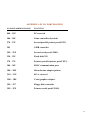
APPENDIX A PC I/O PORT MAPPING
I/O PORT ADDRESS RANGE
FUNCTION
000 – 1FF
PC reserved
200 – 20F
Game controller(Joystick)
278 – 27F
Second parallel printer port(LPT2)
2E1
GPIB controller
2F8 – 2FF
Second serial port(COM2)
320 – 32F
Fixed disk(XT)
378 – 37F
Primary parallel printer port(LPT1)
380 – 38F
SDLC communication port
3B0 – 3BF
Monochrome adapter/printer
3C0 – 3CF
EGA, reserved
3D0 – 3DF
Color/graphics adapter
3F0 – 3F7
Floppy disk controller
3F8 – 3FF
Primary serial port(COM1)
24
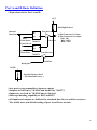
B
U
S
P
C
/
1
0
4
INTERRUPT
CONTROL
LOGIC
ADDRESS
DECODE
LOGIC
INTE
INTP
8255
BUF
DI7 – DI0
DI15 – DI8
DO7 – DO4
DO3 –DO0
APPENDIX B BLOCK DIAGRAM
25
APPENDIX C TECHNICAL REFERENCE
General Usage of Digital Input and Output
Digital signals are usually used for detecting logical status or controlling devices, a
brief description is given below. TTL level signals are developed by most DAS
systems.
TTL or LSTTL Level I/O Connections
TTL LEVEL I/O CONNECTION
TTL Devices
DO
DI
DGND
Connection with CMOS Device – Use a pull-up resistor if you wish to interface to
CMOS devices. This will raise the logic high output level from its minimum TTL
level of 2.4V to +5V suitable for CMOS interface.
VCC
PULL-UP RESISTOR
TTL
CMOS
26
Digital Input for Open/Short Switch Detection – A pull-up resistor must be connected,
especially at long distance wiring, to ensure logic high input level.
+5V
4.7K
DI
Switch
Digital Input for Large Signal
DI
R
Digital Output for relay Driving – The D1 diode is added to protect the IC driver
against the inductive “kickback” from the relay coil.
VCC
D1
DO
27
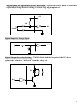
Port A and B Basic Definition
1.Equivalent ckt for Port A and B
VCC
Pull High Resistor
Internal
Data Bus
Line Driver
Data
Write Pulse
D
Q
74LS244
74LS273
Control Port
Data
34 Pin Connector for input
16 Pin Connector for output
DI0 – DI7
DI8 – DI15
DO0 – DO7
D
Q
Control Port
Write Pulse
Line Receiver
74LS273
74LS244
Read pulse
NOTE:
Optional Resistor Pack
( Not Installed Factory )
2.Any port is programmable to input or output.
3.Outputs are driven by 74LS244 and latched by 74LS273.
4.Inputs are received by 74LS244 but not latched.
5.Interrupt handing capability at DO3 and DO7.
6.All inputs and outputs are buffered by standard line drivers and line receivers.
7.The initial state and default setting of port A and B are tri-state.
28
APPENDIX D PC/104 MECHANICAL SPECIFICATION
PC/104 General Description
While the PC and PC/AT architectures have become extremely popular in both
general purpose (desktop) and dedicated (non-desktop) applications, its use in
embedded microcomputer applications has been limited due to the large size of
standard PC and PC/AT motherboards and expansion cards.
This document supplies the mechanical and electrical specifications for a compact
version of the PC/AT bus, optimized for the unique requirements of embedded
systems applications. The specification is herein referred to as “PC/104”, based on
the 104 signal contacts on the two bus connectors (64 pin on P1 plus 40 pin on P2).
Module Dimensions
PC/104 modules can be of two bus types, 8-bit and 16-bit. These correspond to the
PC and PC/AT buses, respectively.
29
APPENDIX D PROGRAMMING 8254 COUNTER/TIMER
Introduction
NETCOM’s NC-910 module uses INTEL 8254 which consist of three independently programmable
16-bit counters for its timing function. Each counter can be programmed to be divided by number
within the range of 2 – 65535. The 8254 is suitable for:
Event counter
Delay time generator
Programmable one-shot
Square wave generator
For detailed information, user should refer to the 8254 Programmable Interval Timer data sheet.
Counter Read/Write and Control Register
There are 4 registers need to program 8254 Time/Counter, including there Read/Write and one
Control register as follows:
Base +0 through Base +3:
Base +0
Base +1
Base +2
Base +3
Counter 0
Read/Write register
Counter 1
Read/Write register
Counter 2
Read/Write register
Control word register
Read/Write register is used to load divisor to select counter, or Read count from selected counter.
Control register is used to determine counter’s operation.
30