1
Programmable System-on-Chip Technology from Cypress Semiconductor
Digital Systems Architecture
Project Report
Submitted by: Abdallah Ismail
Student Number: 100304813
Date: December 3rd 2007
1.0 Introduction
A typical embedded system application makes use of a small processor that coordinates
execution and processing of data between peripherals. Program code is usually stored in
on-chip flash memory, while data is stored and retrieved from on-chip RAM [1].
A System-on-Chip (SOC)-based embedded system is one which uses configurable
hardware surrounding a soft or hard processor core [2]. The purpose of this report is to
study the architecture of Programmable System-on-Chip (PSoC) from Cypress
Semiconductor and compare it to the more conventional FPGA-based SoC architecture.
Next section provides a background on FPGA-based SoC and Cypress PSoC
architectures. The third section studies the configurable digital components of the PSoC
architecture in detail. The fourth section talks about Cypress Programmable Radio-onChip (PRoC) technology and discusses how it could be used to enable wireless
communication between PSoC devices. The fifth section Details the use of PSoC
Designer, an integrated IDE used to design PSoC applications. The sixth section
demonstrates two applications: one PSoC application which demonstrates the concept of
dynamic re-configurability of PSoC devices, and another PRoC application which
establishes a remote control channel between two PRoC devices.
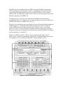
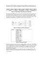
2.0 Background
Conventional FPGA-based SoC architecture consists of configurable logic blocks
(CLB’s), configurable I/O blocks, programmable interconnect, and a soft or hard
processor core [2], as shown in Figure 1 below.
Figure 1: FPGA-based SoC Architecture
The CLB is the basic building block in an FPGA. It contains RAM for lookup tables
(LUT), flip-flops for clocked storage elements, and multiplexers for routing signals to
and from the CLB. Programmable interconnect within the FPGA is used to connect
different CLB’s and I/O blocks together and act as buses to route the signals between the
different components of the FPGA [2].
A hard processor is a fixed processor embedded in the FPGA, and surrounded by
programmable logic [2]. A soft processor is a logic description of a processor than can be
included in the design of an FPGA-based SoC [2].
The low-level of abstraction and general-purpose nature of the building blocks making up
an FPGA makes it a very flexible solution. Design complexity however is high. To
design an FPGA-based SoC application one has to design (or select) a soft or hard
processor, design (or select) the required peripheral set for the application, compile the
design into a gate level description, place and route the design onto the FPGA, and finally
write the application’s software [2].
Similar to an FPGA-based SoC, a PSoC consists of (among other things) a fixed
processor core, a number of configurable digital blocks, and programmable interconnect
[3]. A high level view of the PSoC architecture is shown in Figure 2 below.
Figure 2: Cypress Semi PSoC Architecture
The basic building block in a PSoC is the Digital Block (Digital Block). This is
analogous to a CLB in an FPGA. A Digital Block however is a much higher level of
abstraction than a CLB is.
Figure 3: Digital Block Top Level Block Diagram
A Digital Block consists of the data path, input multiplexers, output de-multiplexers,
configuration registers, and chaining signals [3]. Through the RAM-based configuration
registers, a Digital Block may be configured to perform any one of seven functions: timer,
counter, pulse width modulator (PWM), pseudo random sequence (PRS), cyclic
redundancy check (CRC), SPI, and a full duplex UART [1]. Each Digital Block provides
8 bits of resolution (8-bit timer, 8-bit counter …etc.). Multiple Digital Block’s can be
chained together to provide higher resolution functions [1].
The programmable interconnect enables routing of signals from any Digital Block to any
of the on-chip I/O pins. Furthermore, any Digital Block’s output can be routed to any
Digital Block’s input. Configuring the digital interconnect is again done through RAMbased configuration registers [3].
By fixing the processor core and the component placement, and incorporating a highlevel configurable digital block and interconnect design, PSoC architecture provides its
users with a much simpler embedded system design model while still providing a degree
of flexibility, enough to meet the needs of a large segment of the embedded systems
market [1].
To design a PSoC-based embedded system application, one has to select the function of
each of the digital blocks, route the signals to their proper end-points, and write the
application’s software in C or Assembly language. Knowledge of hardware design is not
required [1]. The next section looks at the PSoC architecture in detail.
3.0 PSoC Architecture
Figure 4: PSoC top-level block diagram
A PSoC consists of four main elements [3], as shown above in the Figure 4:
1- The PSoC core is common to all PSoC families. It contains a proprietary 24MHz
M8C CPU core, on-chip RAM and flash memories, multiple clock sources, a
sleep-and-watchdog timer, and an interrupt controller [1].
2- The Digital System contains a number of digital blocks. Each digital block can be
configured (and reconfigured) to perform one of several digital functions such as
32-bit timer, 16-bit PWM, UART and SPI [1].
3- The Analog System contains a number of analog blocks. Each analog block can
be configured and reconfigured to perform one of several analog functions such as
filters, amplifiers, tone generators, ADCs, and DACs [1].
4- Finally, System Resources provide additional PSoC capability. They include
multiply-accumulates (MAC), decimators, I2C, a Switch Mode Pump (SMP), and
a full speed (12Mbps) USB [1].
All of the elements mentioned above are connected through a configurable digital and
analog interconnect switching fabric which enables different blocks to be connected to
each other and to drive or be driven from any of the I/O pins available on-chip. The
Analog System, the Digital System, and the interconnect form the configurable core of
the PSoC device [3].
This report is concerned with the reconfigurable digital components of the PSoC, as these
components most closely relate to the reconfigurable-hardware concept found in FPGAbased SoC’s. For information on the rest of the system, including the PSoC core, the
Analog System, and the System Resources please refer to [1] and [3].
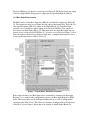
3.1 Digital System
Figure 5: PSoC Digital System Block Diagram
The configurable digital system in a PSoC consists of three main components [3]:
1. The Global Digital Interconnect (GDI)
2. The Row Digital Interconnect (RDI)
3. The digital blocks
The Digital Blocks can be configured to perform one of seven peripheral functions. The
RDI and GDI form the interconnect that allows signal routing to and from the digital
blocks. The RDI connects the outputs and inputs of digital blocks to the GDI. The GDI in
turn connects the RDI to the on-chip I/O pins. Together, the RDI and GDI can route the
inputs and outputs of any of the digital blocks between each other and to any of the onchip I/O pins. Figure 6 below shows a typical PSoC application that uses a Pulse-WidthModulated (PWM) Output. Digital Block 0 is configured as an 8-bit PWM whose output
is routed to pin 0 of port 0 through the configurable digital interconnect.
Figure 6: Digital Block_0 is configured as an 8-bit PWM whose output is routed to
pin 0 of port 0 through the digital interconnect. GDI buses are vertical green. RDI
Input bus is horizontal red. RDI output bus is horizontal blue. Digital blocks are the
4 blocks shown in the middle of the diagram
Configuration of the digital blocks and the digital interconnect is done by programming
various RAM-based registers. Specific configurations of these registers can be stored in
the on-chip flash and loaded into RAM whenever needed, thus allowing for dynamic
reconfiguration of the PSoC.
The next subsection studies the Global Digital Interconnect (GDI), the following
subsection studies the Row Digital Interconnect (RDI), and the last subsection studies the
Digital Block. The three subsections will therefore cover the configurable digital
components of PSoC devices.
3.1.1 Global Digital Interconnect
The GDI consists of four 8-bit buses which allow signals to pass to/from the device pins
from/to the core of the PSoC device [3]. Two of the buses are input buses called Global
Input Odd (GIO) and Global Input Even (GIE) [3]. The other two are output buses called
Global Output Odd (GOO) and Global Output Even (GOE) [3]. Odd busses connect to
odd I/O ports such as ports 1, 3, 5, and 7. Similarly, even buses connect to even I/O ports
such as ports 0, 2, 4, and 6.
The four GDI buses are shown as vertical green in Figure 6. The Figure shows the output
of the first Digital Block being routed to output pin 0 of port 0 through the GOE_0.
3.1.2 Row Digital Interconnect
The RDI consists of four Row Input nets (RI[3:0]) and four Row Output nets (RO[3:0])
[3]. The input nets can be seen in Figure 6 as the four red horizontal lines. Their job is to
route signals from the GDI to the inputs of the Digital Blocks [3]. Each Row Input
contains a 4-to-1 multiplexer whose inputs are fed by four GDI lines. The outputs of
these muxes are Row Inputs (RI[x]) [3]. This means that any single Row Input net can
connect to one of four possible GDI lines [3], as can be seen to the left of Figure 7 below.
Since the inputs to the muxes are unique to each mux, a complete Row Input has access
to every global input line in a PSoC device [3].
Figure 7: Digital PSoC Block Row Structure
Each of the four muxes in a Row Input can be controlled by writing to the Row Input
Register [3]. As with all other configuration registers, the Row Input Register is RAMbased. This means that it can be configured during start up, as well as during normal
operation of the PSoC device. This allows for dynamic reconfiguration of the input nets
of the PSoC device. Figure 8 below shows an example in which Digital Block 0 is
configured as an input capture 8-bit timer whose input is fed from pin 0 of port 0 through
Row Input RI[0].
Figure 8: Digital Block 0 is configured as an 8-bit input-capture Timer whose input
is fed from pin 0 of port 0 through the digital interconnect. Row Input nets are
horizontal red.
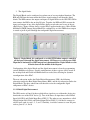
The Row Output nets are a bit more involved than the Row Input nets, as can be seen to
the right of Figure 7. In the Figure, the block labeled Lx represents a 2-input look-up
table (LUT). The LUT allows the user to specify any one of 16 logic functions that
should be applied to the two inputs [3]. A more detailed structure of one Row Output is
shown in figure 9 below. The 16 logic functions are shown in table 1 [3].
Figure 9: Example of LUT0 configuration
Table 1: LUT logic functions
The output of a LUT can drive as many as 4 GDI lines, through configurable tri-state
buffers [3]. The LUT’s inputs, outputs, and logic functions are configured through RAMbased registers which can be loaded with settings stored in flash memory after power up
or during normal operation of the device, thus allowing for initial configuration and
dynamic reconfiguration of signal routing from the digital blocks to the output pins.
Row Output RO[3:0] are shown as horizontal blue lines in Figure 6 and Figure 8.
3.1.3 Digital Blocks
Figure 10: Digital Block Top Level Block Diagram
A Digital Block consists of the data path, input multiplexers, output de-multiplexers,
configuration registers, and chaining signals [3]. Through the RAM-based configuration
registers, a Digital Block may be configured to perform any one of seven functions: timer,
counter, pulse width modulator (PWM), pseudo random sequence (PRS), cyclic
redundancy check (CRC), SPI, and a full duplex UART [3]. Each Digital Block provides
8 bits of resolution (8-bit timer, 8-bit counter …etc.). Multiple Digital Blocks can be
chained together to provide functions with higher resolution [3].
There are three inputs to a Digital Block: Clock, data, and auxiliary [3]. Typically, each
function has a clock and a data input that can be selected from one of 16 possible input
sources, through the 16-to-1 input mux [3]. This leaves the auxiliary input, which is
selected through the 4-to-1 mux. The auxiliary input is designed specifically to act as the
SPI Slave-Select signal for a Digital Block configured in Slave SPI mode [3].
There are five main outputs to a Digital Block: A primary output, an auxiliary output, a
chaining signal, and a block interrupt [3]. The primary and auxiliary outputs can be
configured to drive the RDI Row Output bus through two 1-to-4 de-muxes [3]. The
chaining signals propagate information from one Digital Block to the next, thus allowing
functions with higher resolutions to be implemented [3]. The block interrupt is functiondependant and is used to trigger a vector-based interrupt signal to the PSoC core [3].
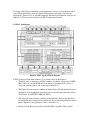
The input signals, the output signals, and the function of the data path are configured by
seven RAM-based registers: Three Data Registers, a Control Register, a Function
Register, an Input Register, and an Output Register [3].
The definition of most of these registers is function-dependant. For example, the Control
Register contains the function control and status bits for the selected function. The
definition for each bit in the Control Register changes depending on the selected function,
as shown in table 2 below [3].
Table 2: Control Register Description
Similarly, the definition for the three data registers changes depending on the selected
function of the Digital Block. For example, when the Timer function is selected, Data
Register 0 is automatically configured to hold the Count value, Data Register 1 is
automatically configured to hold the Period, and Data Register 2 is automatically
configured to hold the Capture/Compare value [3]. Alternately, if the SPI Master function
is selected, then Data Register 0 is automatically configured to function as the serial
shifter, Data Register 1 is automatically configured to function as the transmit buffer, and
Data Register 2 is automatically configured to function as the receive buffer [3].
This leaves the Function Register, the Input Register, and the Output Register. The
Function register enables selection of the intended function of the Digital Block [3]. The
Input Register enables configuration of the three input signals of the Digital Block [3].
The Output Register enables the configuration of the output signals of the Digital Block
[3].
Since all seven registers are RAM-based, several Digital Block settings can be stored in
flash memory and later reloaded as required by the application, thus allowing for the
function of each Digital Block to be dynamically reconfigured.
4.0 Programmable Radio-on-Chip Technology
Programmable Radio-on-Chip (PRoC) technology combines PSoC technology with a
fully-programmable on-chip wireless transceiver [4].
Figure 11: PRoC Block Diagram
The wireless transceiver portion is a complete SPI-to-antenna radio modem designed to
operate in the 2.4GHz ISM band [5]. It contains a low-Intermediate Frequency (low-IF)
front end, a Gaussian Frequency Shift Keying (GFSK) modem, and a reconfigurable
Direct Sequence Spread Spectrum (DSSS) baseband processor [5]. A
Serializer/Deserializer (SERDES) block provides byte-level framing of transmit and
receive data, and an SPI interface provides connectivity to the rest of the PSoC [5].
Figure 12: Wireless transceiver simplified block diagram
The transmit operation begins by loading a new byte into the Serializer using the SPI
interface of the radio. The Serializer in turn loads the byte into a serial shift register
whose output feeds the DSSS baseband processor [5]. The output of the Serializer is
programmable at 3 different data rates: 16kbps, 32kbps, and 64kbps [5].
The DSSS baseband processor uses Gold Codes to spread each incoming bit into a
maximum of 64 chips [5]. Gold Codes are chosen due to their excellent autocorrelation
and cross-correlation properties. The number of chips per bit (cpb), also known as the
spreading factor, depends on the selected data rate. 64cpb is used when 15kbps is selected,
32cpb is used when 32kbps is selected, and 16cpb is used when 64kbps is selected [5].
The output of the baseband processor is therefore a fixed 1Mcps baseband signal.
The output of the DSSS baseband processor feeds a GFSK modulator. This modulator
uses a DSP-based vector to convert the baseband signal to an accurate IF GFSK carrier
[5]. The modulated signal is then mixed up to the appropriate frequency channel by
tuning the frequency synthesizer to that channel. The frequency synthesizer is tunable
over 80 1MHz channels with channel 0 starting at 2.400GHz and channel 79 ending at
2.479GHz. The modulated signal occupies a bandwidth of 1MHz [5].
The output of the mixer feeds an integrated power amplifier that provides a
programmable output power control range of 30dB in seven steps, as shown in Table 3
below [5].
Table 3: Internal PA Output Power Step Table
On the receive side, an FM detector with automatic data slicer demodulates the mixed
down GFSK signal into baseband [5]. The DSSS baseband processor correlates the
incoming baseband signal with the programmed Gold Code sequence, thus de-spreading
the signal, and feeds the De-Serializer with the de-spread signal. The de-serializer issues
an interrupt to the external processor which in turn reads the newly received byte through
the SPI interface [5].
As mentioned above, programmable features in the radio include the Gold Code selection,
frequency channel, data rate, and output power. Other programmable features include
power management and RSSI functionality [5].
5.0 Designing with PSoC Designer
PSoC Designer is an Integrated Development Environment (IDE) used to develop
applications for PSoC and PRoC devices. It contains a Device Editor, an Application
Editor, a C-Compiler, an Assembler, a Builder, and a Real-Time Debugger [6].
The Device Editor is really what separates PSoC Designer from other microcontrollerbased development environments. It allows GUI-based configuration of the entire PSoC,
as well as automatically generates all the necessary API specific to an application [6].
Figure 13: Selected (Yet-to-be-placed) user modules
Figure 13 above shows a snapshot of the Device Editor. PSoC global resources can be
configured at the top left of the figure. I/O ports can be configured at the lower left of the
figure. Digital and Analog Blocks can be selected, placed, and routed in the main area in
the middle. All of this is done graphically.
After configuring, placing and routing a design, the Device Editor will generate
application files based on the device configuration. These application files include
Application Programming Interface (API) and Interrupt Service Routine (ISR) shells [6].
The Device Editor will also create a datasheet based on the device configuration [6].
Once the application files are generated, the Application Editor can be used to create the
application code and build it into a HEX file. The HEX file is then loaded into the on-
chip flash memory of the target device. Flash-programming is performed using the PSoC
Programmer tool which accompanies PSoC Designer [7].
6.0 PSoC Applications
Two applications are implemented and their hardware/firmware described in this section.
The first application generates multiple PWM signals from a single PWM generator and
is used to illustrate the concept of dynamic re-configurability of the PSoC device. The
second application establishes a point-to-point Remote Control channel using PRoC
technology. The purpose of this application is to illustrate the ease with which a Spread
Spectrum wireless application could be developed using PRoC technology.
6.1 Application 1: Multiple PWM Signal Generation
The first application generates multiple PWM signals from a single PWM generator. The
purpose of this application is to demonstrate the dynamic re-configurability of the Digital
system.
First, the PSoC is graphically configured as shown in the figure below.
Figure 14: Application configuration
As can be seen from the figure, Digital Blocks 0 and 1 are configured to function as a 16bit PWM. RDI0 (the horizontal blue lines) connects the output of the PWM to I/O pins
1_0 to 1_3. Reconfiguring the output of the PWM at run-time to different rows of RDI0
will route the PWM signal to different pins. For example, configuring the output of the
PWM to row 0 of RDI0 connects the PWM output to pin 1_0, while reconfiguring the
output of the PWM to row 1 of RDI0 connects the PWM output to pin 1_1. This enables
us to generate multiple PWM signals from a single PWM generator.
The output of a Digital Block is configured through its RAM-based Output Register [3],
shown below. Bits 1 and 0 select the RDI row to which the output of the block connects.
Figure 15: Digital Block Output Register bit definitions
The output of the PWM connects to one pin at a time. This means that all other pins are
left unconnected for a small period of time. To avoid glitches on the unconnected pins,
they must be driven low when not in use. This is done by reconfiguring the LUT which
drives these pins to false [3]. The operation of the LUT was discussed in section 3.1.2. Its
architecture and truth table are repeated here for the reader’s convenience.
Figure 16: Example of LUT0 configuration
Table 4: LUT logic functions
Application code is based on a Finite State Machine (FSM) with four states. The PWM is
driven by a 60 KHz clock. The period is set to 30000 (half a second), and the pulse width
is set to 15000 (quarter of a second). The PWM issues an interrupt every half a second.
The interrupt is used to trigger the next state transition in the FSM, during which the
reconfiguration takes place.
Main initializes the PWM FSM, enables global interrupts, and loops indefinitely. The
ISR calls the PWM task which triggers the next transition in the FSM. Application code
is shown below.
//---------------------------------------------------------------------------// C main line
//---------------------------------------------------------------------------#include <m8c.h>
// part specific constants and macros
#include "PSoCAPI.h" // PSoC API definitions for all User Modules
//External function prototypes
extern void pwm1_init(void);
extern void task_pwm1(void);
void main()
{
//initialize the PWM task
pwm1_init();
//enable global interrupts and loop indeinitely
M8C_EnableGInt;
while (TRUE);
}
//PWM ISR
//Triggers every 0.5 second on PWM terminal count
//calls the PWM task
#pragma interrupt_handler pwm1_isr
void pwm1_isr(void)
{
task_pwm1();
}
//---------------------------------------------------------------------------// PWM FSM
//---------------------------------------------------------------------------#include <m8c.h>
// part specific constants and macros
#include "PSoCAPI.h" // PSoC API definitions for all User Modules
//state definitions
#define STATE_PWM_P10
#define STATE_PWM_P11
0
1
//output PWM on Port 1 Pin 0
//output PWM on Port 1 Pin 1
#define STATE_PWM_P12
#define STATE_PWM_P13
2
3
//Bit masks for RDI LUT registers
#define RDIxLT0_LUT0_A
#define RDIxLT0_LUT0_FALSE
#define RDIxLT0_LUT1_A
#define RDIxLT0_LUT1_FALSE
#define RDIxLT1_LUT2_A
#define RDIxLT1_LUT2_FALSE
#define RDIxLT1_LUT3_A
#define RDIxLT1_LUT3_FALSE
//output PWM on Port 1 Pin 2
//output PWM on Port 1 Pin 3
0x03
0x00
0x30
0x00
0x03
0x00
0x30
0x00
//Bit masks for Digital Blocks Output Registers
#define DxBxxOU_AUXCLK_SYNC
0x40
#define DxBxxOU_OUTEN
0x04
#define DxBxxOU_ROW0
0x00
#define DxBxxOU_ROW1
0x01
#define DxBxxOU_ROW2
0x02
#define DxBxxOU_ROW3
0x03
//variable which holds the current state of the FSM
static BYTE state;
//initializes the PWM task
void pwm1_init(void);
//the PWM task
//implements an FSM which switches the output of the
//PWM to four different I/O pins: P1_0 to P1_3
void task_pwm1(void);
//Initializes the PWM task
void pwm1_init(void)
{
//initialize first state
state = STATE_PWM_P10;
//enable the block interrupt and start the PWM
PWM1_EnableInt();
PWM1_Start();
}
//the PWM task
//implements an FSM which switches the output of the
//PWM to four different I/O pins: P1_0 to P1_3
void task_pwm1(void)
{
//the FSM contains 4 states connected in a circular manner:
//the first state connects to 2nd, 2nd to 3rd, 3rd to 4th,
//and 4th back to 1st.
//Each state performs the following:
//1-stop the PWM
//2-reconfigure the output of the PWM to the proper pin
//3-reconfigure the drive of all other pins to low
//4-restart the PWM
//5-go to next state
switch (state)
{
case STATE_PWM_P10:
//stop the PWM
PWM1_Stop();
//reconfigure output of PWM to pin 1_0
PWM1_OUTPUT_MSB_REG = DxBxxOU_AUXCLK_SYNC |
DxBxxOU_OUTEN | DxBxxOU_ROW0;
//reconfigure the drive of pins 1_1, 1_2, and 1_3 to low
RDI0LT0 = RDIxLT0_LUT0_A | RDIxLT0_LUT1_FALSE;
RDI0LT1 = RDIxLT1_LUT2_FALSE | RDIxLT1_LUT3_FALSE;
//restart the PWM
PWM1_Start();
//go to next state
state = STATE_PWM_P11;
break;
case STATE_PWM_P11:
PWM1_Stop();
PWM1_OUTPUT_MSB_REG = DxBxxOU_AUXCLK_SYNC |
DxBxxOU_OUTEN | DxBxxOU_ROW1;
RDI0LT0 = RDIxLT0_LUT0_FALSE | RDIxLT0_LUT1_A;
RDI0LT1 = RDIxLT1_LUT2_FALSE | RDIxLT1_LUT3_FALSE;
PWM1_Start();
state = STATE_PWM_P12;
break;
case STATE_PWM_P12:
PWM1_Stop();
PWM1_OUTPUT_MSB_REG = DxBxxOU_AUXCLK_SYNC |
DxBxxOU_OUTEN | DxBxxOU_ROW2;
RDI0LT0 = RDIxLT0_LUT0_FALSE | RDIxLT0_LUT1_FALSE;
RDI0LT1 = RDIxLT1_LUT2_A | RDIxLT1_LUT3_FALSE;
PWM1_Start();
state = STATE_PWM_P13;
break;
case STATE_PWM_P13:
PWM1_Stop();
PWM1_OUTPUT_MSB_REG = DxBxxOU_AUXCLK_SYNC |
DxBxxOU_OUTEN | DxBxxOU_ROW3;
RDI0LT0 = RDIxLT0_LUT0_FALSE | RDIxLT0_LUT1_FALSE;
RDI0LT1 = RDIxLT1_LUT2_FALSE | RDIxLT1_LUT3_A;
PWM1_Start();
state = STATE_PWM_P10;
break;
}
}
6.2 Application: Remote Control
The second application establishes a point-to-point Remote Control channel in the
2.4GHz ISM band. The purpose of this application is to illustrate the ease with which a
Spread Spectrum wireless application can be developed using PRoC Technology.
The application consists of two components: Transmitter and Receiver. The hardware for
both nodes is shown below.
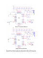
Figure 17: Transmitter Hardware
Figure 18: Receiver Hardware
The transmitter continuously samples the switch connected to P0_2. When pressed, the
transmitter sends a packet containing four predefined bytes to the receiver on channel 0
of the 2.4GHz band. The receiver listens to that channel continuously and when it
receives a valid packet it toggles the LED connected to P1_0.
The Device Editor in PSoC Designer is first used to graphically configure the transmitter
and receiver nodes. The Device Editor then generates all the necessary API for using the
device, including functions to establish wireless communication. The Application Editor
is then used to write the application code for each of the nodes. Transmitter and Receiver
codes are shown below.
//---------------------------------------------------------------------------// TRANSMITTER
//---------------------------------------------------------------------------#include <m8c.h>
// part specific constants and macros
#include "PSoCAPI.h" // PSoC API definitions for all User Modules
#define LED_PORT
#define LED
#define SWITCH_PORT
#define SWITCH
PRT2DR
0x80
PRT0DR
0x04
#define PACKET_LENGTH 4
#define MESSAGE_EMPTY
#define MESSAGE_TIMEOUT
0
1
//macros used to sample a switch
#define WAIT_FOR_PRESS
#define WAIT_FOR_RELEASE
while(SWITCH_PORT & SWITCH)
while(!(SWITCH_PORT & SWITCH))
//a 64-chip Gold Code
const BYTE pn_code[8] = {0x36, 0xF3, 0x8C, 0xB5, 0x11, 0x4A, 0xCA, 0x1F};
BYTE message;
//a predefined packet to be used as a command to toggle a LED at the receiver
BYTE packet[PACKET_LENGTH] = {0x12, 0x34, 0x56, 0x78};
//function used to debounce a switch once pressed or released
//implements a 40ms blocking wait
void debounce_switch(void);
//Main
void main()
{
//initialize the transceiver
Radio_Start();
//set the 64-chip Gold Code stored in flash
Radio_SetPnCode(pn_code);
//set channel 0 to be used for transmission
Radio_SetChannel(0);
//enable global interrupts
M8C_EnableGInt;
//do forever
while (TRUE) {
//wait for switch press
WAIT_FOR_PRESS;
//debounce
debounce_switch();
//wait for switch release
WAIT_FOR_RELEASE;
//debounce
debounce_switch();
//tx packet
LED_PORT ^= LED;
Radio_SendData(PACKET_LENGTH, packet);
}
}//end main
//implements a 40ms blocking wait
//used to debounce a switch press and release
//uses timer interrupt
void debounce_switch(void)
{
//set message to EMPTY, enable timer interrupt and start the timer
//Timer ISR will set message to TIMEOUT after 40ms
message = MESSAGE_EMPTY;
Timer_EnableInt();
Timer_Start();
//wait for timer ISR to set message to TIMEOUT
while (message == MESSAGE_EMPTY);
//stop timer
Timer_Stop();
}
//Timer ISR
//triggers when timer expires
#pragma interrupt_handler timer_isr
void timer_isr(void)
{
//set message to TIMEOUT
message = MESSAGE_TIMEOUT;
}//end of file
//---------------------------------------------------------------------------// RECEIVER
//---------------------------------------------------------------------------#include <m8c.h>
// part specific constants and macros
#include "PSoCAPI.h" // PSoC API definitions for all User Modules
#define LED_PORT
#define LED
PRT1DR
0x01
#define TIMEOUT_1S
60000
#define PACKET_LENGTH 4
//same 64-chip Gold Code used at the transmitter side
const BYTE pn_code[8] = {0x36, 0xF3, 0x8C, 0xB5, 0x11, 0x4A, 0xCA, 0x1F};
//used to buffer an incoming packet
BYTE packet[PACKET_LENGTH];
BYTE valid[PACKET_LENGTH];
void main()
{
BYTE length;
//initialize the transceiver
Radio_Start();
//set the Gold Code stored in flash
Radio_SetPnCode(pn_code);
//set channel 0 to be used in reception
Radio_SetChannel(0);
//do forever
while(TRUE) {
//try to receive a 4-byte packet within a 1 second timeout
//blocking read
length = Radio_bReadData(PACKET_LENGTH, packet, valid, TIMEOUT_1S);
//check that the packet length is correct
if (length != PACKET_LENGTH) continue;
//check that the command for toggling the LED is correct
if ((packet[0] == 0x12) && (packet[1] == 0x34) && (packet[2] == 0x56) &&
(packet[3] == 0x78)) {
LED_PORT ^= LED;
}
}
}//end of main
7.0 Conclusion
The fine-configurability of FPGA-based SoC’s provides an extremely flexible platform
that is both hardware and software programmable. The drawback to such architecture
however is the design complexity present and the complex hardware skills required to
mold an FPGA-based SoC into the desired application.
PSoC technology from Cypress Semiconductor tackles the design complexity and the
required hardware skill issues by fixing the components that are common to most
embedded systems including the processor, and incorporating a high-level configurable
Digital Block and interconnect design. In effect, PSoC architecture provides its users with
a much simpler embedded system design model while still providing a degree of
flexibility, enough to meet the needs of a large segment of the embedded systems market.
Moreover, PRoC technology adds Spread Spectrum wireless capabilities to the mix,
which enables the establishment of wireless communication channels between PSoC
devices with relative ease.
Design and development of both PSoC and PRoC technologies is made easy using the
PSoC Designer IDE. The IDE allows GUI-based configuration of a device, and the
generation of all the necessary API specific to that device. This process considerably
eases firmware design and increases its reliability.
8.0 Reference
[1] Monte Mar, Bert Sullam, Eric Blom, “Field Programmable Mixed-Signal SoC Offer
More Levels of Integration”, Cypress Microsystems Inc, May 13 2002, Available at:
http://www.planetanalog.com/showArticle.jhtml?articleID=12802111
[2] Bob Zeidman, “Introduction to Programmable Systems on a Chip”, Zeidman
Technologies, 07/27/2005, Available at:
http://www.pldesignline.com/showArticle.jhtml;jsessionid=SIR3M5OKG3NDUQSN
DLPSKH0CJUNN2JVN?articleID=166403118&queryText=bob+zeidman
[3] Cypress Semiconductor, “PSoC Mixed Signal Array: Technical Reference Manual”,
Cypress Semiconductor, PSoC TRM version 2.10, 2006, available at
www.cypress.com
[4] Cypress Semiconductor, “CYWUSB6953: Wireless PRoC Flash Programmable MCU
+ Radio”, Cypress Semiconductor, August 19, 2005
[5] Cypress Semiconductor, “CYWUSB6935: WirelessUSB LR 2.4-GHz DSSS Radio
SoC”, Cypress Semiconductor, November 18, 2004
[6] Cypress Semiconductor, “PSoC Designer: IDE User Manual”, Cypress
Semiconductor, Document # 38-12002 Rev E, 2005
[7] Cypress Semiconductor, “PSoC Designer: Programmer User Guide”, Cypress
Semiconductor, Version 1.22, 2005