1
University of Southampton Research Repository
ePrints Soton
Copyright © and Moral Rights for this thesis are retained by the author and/or other
copyright owners. A copy can be downloaded for personal non-commercial
research or study, without prior permission or charge. This thesis cannot be
reproduced or quoted extensively from without first obtaining permission in writing
from the copyright holder/s. The content must not be changed in any way or sold
commercially in any format or medium without the formal permission of the
copyright holders.
When referring to this work, full bibliographic details including the author, title,
awarding institution and date of the thesis must be given e.g.
AUTHOR (year of submission) "Full thesis title", University of Southampton, name
of the University School or Department, PhD Thesis, pagination
http://eprints.soton.ac.uk
UNIVERSITY OF SOUTHAMPTON
FACULTY OF ENGINEERING, SCIENCE AND MATHEMATICS
School of Electronics and Computer Science
A Comprehensive Scheme for
Reconfigurable Energy-Aware
Wireless Sensor Nodes
by
Alexander Stewart Weddell
Thesis for the degree of Doctor of Philosophy
May 2010
UNIVERSITY OF SOUTHAMPTON
ABSTRACT
FACULTY OF ENGINEERING, SCIENCE AND MATHEMATICS
SCHOOL OF ELECTRONICS AND COMPUTER SCIENCE
Doctor of Philosophy
A COMPREHENSIVE SCHEME FOR RECONFIGURABLE
ENERGY-AWARE WIRELESS SENSOR NODES
by Alexander Stewart Weddell
Wireless sensor nodes are devices that perform measurements (of parameters such as
temperature or vibration) and communicate over a wireless medium. A key benefit is
that they can operate autonomously. Nodes are commonly battery-powered so that
they can be deployed rapidly without the need to install a wired power supply; however,
batteries must be changed when depleted and this can impose a costly maintenance requirement. Energy harvesting is an emerging field, which offers the possibility for nodes
to be powered indefinitely from environmental energy (such as light, vibration, or temperature difference). The power generated from environmental energy is often limited
and variable, and nodes must be able to adapt their operation to take account of the
power available. There have been a number of demonstrations of wireless sensor nodes
powered from harvested energy, but existing demonstrators are tailored for specific types
of energy resource (constraining their use to applications with suitable energy availability). The existing interfaces between the energy hardware and the nodes’ embedded
software is bespoke and limited to specific devices, so it is impossible to exchange the
energy hardware to adapt to differing energy availability.
The work described in this thesis delivers a comprehensive scheme for reconfigurable
energy-aware sensor nodes, which overcomes the limitations of the existing systems and
allows the energy hardware for sensor nodes to be connected together in a plug-and-play
manner. The scheme has been evaluated by way of a prototype which accommodates a
range of energy devices. The main contributions of this research are threefold: firstly, the
system is enabled by a new hardware interface between the energy devices and sensor
node; secondly, an embedded software structure is implemented to interface with the
energy hardware; and thirdly, efficient energy-aware modules compliant with the scheme
have been produced. The combined result is a novel energy subsystem for wireless sensor
nodes that supports a range of energy devices and can deliver energy-aware operation
for a range of microcontroller platforms, while imposing a minimal additional resource
requirement to deliver this functionality.
Contents
Declaration of Authorship
xvii
Acknowledgements
xix
Nomenclature
xxiii
Abbreviations
xxv
1 Introduction
1.1 Wireless autonomous sensing .
1.2 Outline of the AEASN project
1.3 Justification for this research .
1.4 Contributions of this research .
1.5 What is ‘reconfigurability’ ? . .
1.6 Publications . . . . . . . . . . .
1.7 Document structure . . . . . .
.
.
.
.
.
.
.
.
.
.
.
.
.
.
.
.
.
.
.
.
.
.
.
.
.
.
.
.
.
.
.
.
.
.
.
.
.
.
.
.
.
.
.
.
.
.
.
.
.
.
.
.
.
.
.
.
.
.
.
.
.
.
.
.
.
.
.
.
.
.
.
.
.
.
.
.
.
.
.
.
.
.
.
.
.
.
.
.
.
.
.
.
.
.
.
.
.
.
.
.
.
.
.
.
.
.
.
.
.
.
.
.
.
.
.
.
.
.
.
.
.
.
.
.
.
.
2 Background: Energy, Sensing, and Wireless Communication
2.1 Introduction . . . . . . . . . . . . . . . . . . . . . . . . . . . . .
2.2 Energy storage . . . . . . . . . . . . . . . . . . . . . . . . . . .
2.2.1 Motivations and overview . . . . . . . . . . . . . . . . .
2.2.2 Non-rechargeable (primary) batteries . . . . . . . . . . .
2.2.3 Rechargeable (secondary) batteries . . . . . . . . . . . .
2.2.4 Supercapacitors . . . . . . . . . . . . . . . . . . . . . . .
2.2.5 Other energy storage mechanisms . . . . . . . . . . . . .
2.2.6 Discussion . . . . . . . . . . . . . . . . . . . . . . . . . .
2.3 Energy harvesting and wireless power transfer . . . . . . . . . .
2.3.1 Motivations and overview . . . . . . . . . . . . . . . . .
2.3.2 Photovoltaics . . . . . . . . . . . . . . . . . . . . . . . .
2.3.3 Vibration energy harvesting . . . . . . . . . . . . . . . .
2.3.4 Thermoelectric energy generation . . . . . . . . . . . . .
2.3.5 Small-scale fluid flow . . . . . . . . . . . . . . . . . . . .
2.3.6 Human power . . . . . . . . . . . . . . . . . . . . . . . .
2.3.7 Inductive and RF energy transfer . . . . . . . . . . . . .
2.3.8 Hybrid energy harvesting technologies . . . . . . . . . .
2.3.9 Summary and discussion . . . . . . . . . . . . . . . . . .
2.4 Technologies for intelligent sensing . . . . . . . . . . . . . . . .
2.4.1 The IEEE 1451 standards family . . . . . . . . . . . . .
v
.
.
.
.
.
.
.
.
.
.
.
.
.
.
.
.
.
.
.
.
.
.
.
.
.
.
.
.
.
.
.
.
.
.
.
.
.
.
.
.
.
.
.
.
.
.
.
.
.
.
.
.
.
.
.
.
.
.
.
.
.
.
.
.
.
.
.
.
.
.
.
.
.
.
.
.
.
.
.
.
.
.
.
.
.
.
.
.
.
.
.
.
.
.
.
.
.
.
.
.
.
.
.
.
.
.
.
.
.
.
.
.
.
.
.
.
.
.
.
.
.
.
.
.
.
.
.
.
.
.
.
.
.
.
.
.
.
.
.
.
.
.
1
1
3
4
6
8
8
9
.
.
.
.
.
.
.
.
.
.
.
.
.
.
.
.
.
.
.
.
11
11
11
11
12
14
16
16
17
18
18
18
20
25
27
28
29
30
30
32
32
vi
CONTENTS
2.4.2 Transducer electronic data sheets . . . . . . . . . . .
2.4.3 Extensions to the electronic data sheet concept . . .
2.4.4 System management schemes . . . . . . . . . . . . .
2.4.5 Discussion . . . . . . . . . . . . . . . . . . . . . . . .
2.5 Wireless communication protocols . . . . . . . . . . . . . .
2.5.1 Overview . . . . . . . . . . . . . . . . . . . . . . . .
2.5.2 RF-based methods . . . . . . . . . . . . . . . . . . .
2.5.3 Alternative communication methods . . . . . . . . .
2.5.4 Networking and routing . . . . . . . . . . . . . . . .
2.5.5 Discussion . . . . . . . . . . . . . . . . . . . . . . . .
2.6 Energy-aware operation . . . . . . . . . . . . . . . . . . . .
2.6.1 Energy-aware routing . . . . . . . . . . . . . . . . .
2.6.2 Energy-adaptive behaviour . . . . . . . . . . . . . .
2.6.3 Achieving energy awareness . . . . . . . . . . . . . .
2.6.4 Overall lifetime prediction and extension . . . . . . .
2.6.5 Discussion . . . . . . . . . . . . . . . . . . . . . . . .
2.7 Wireless sensor node technologies . . . . . . . . . . . . . . .
2.7.1 Microcontrollers, transceivers, and system-on-chip .
2.7.2 Commercially-available sensor nodes . . . . . . . . .
2.7.3 Discussion . . . . . . . . . . . . . . . . . . . . . . . .
2.8 Software and algorithm development . . . . . . . . . . . . .
2.8.1 Software structures . . . . . . . . . . . . . . . . . . .
2.8.2 Operating systems . . . . . . . . . . . . . . . . . . .
2.8.3 Discussion . . . . . . . . . . . . . . . . . . . . . . . .
2.9 Existing systems . . . . . . . . . . . . . . . . . . . . . . . .
2.9.1 Wireless sensor system deployments . . . . . . . . .
2.9.2 Systems featuring a single form of energy harvesting
2.9.3 Systems integrating multiple energy resources . . . .
2.9.4 Discussion . . . . . . . . . . . . . . . . . . . . . . . .
2.10 Summary . . . . . . . . . . . . . . . . . . . . . . . . . . . .
.
.
.
.
.
.
.
.
.
.
.
.
.
.
.
.
.
.
.
.
.
.
.
.
.
.
.
.
.
.
.
.
.
.
.
.
.
.
.
.
.
.
.
.
.
.
.
.
.
.
.
.
.
.
.
.
.
.
.
.
3 Development: Towards a Reconfigurable Energy Subsystem
3.1 Introduction . . . . . . . . . . . . . . . . . . . . . . . . . . . . .
3.2 Design for reconfigurability . . . . . . . . . . . . . . . . . . . .
3.2.1 Plug-and-play energy subsystem . . . . . . . . . . . . .
3.2.2 Modular design . . . . . . . . . . . . . . . . . . . . . . .
3.2.3 Usage scenario . . . . . . . . . . . . . . . . . . . . . . .
3.2.4 Major challenges and strategy . . . . . . . . . . . . . . .
3.3 Energy Electronic Data Sheet (EEDS) . . . . . . . . . . . . . .
3.3.1 Overview and justification . . . . . . . . . . . . . . . . .
3.3.2 Data sheet format . . . . . . . . . . . . . . . . . . . . .
3.3.3 Hardware and interrogation method . . . . . . . . . . .
3.4 Common Hardware Interface (CHI) . . . . . . . . . . . . . . . .
3.4.1 Overview and justification . . . . . . . . . . . . . . . . .
3.4.2 EEDS interface . . . . . . . . . . . . . . . . . . . . . . .
3.4.3 Interface format . . . . . . . . . . . . . . . . . . . . . .
3.4.4 Integration of multiple energy sources . . . . . . . . . .
.
.
.
.
.
.
.
.
.
.
.
.
.
.
.
.
.
.
.
.
.
.
.
.
.
.
.
.
.
.
.
.
.
.
.
.
.
.
.
.
.
.
.
.
.
.
.
.
.
.
.
.
.
.
.
.
.
.
.
.
.
.
.
.
.
.
.
.
.
.
.
.
.
.
.
.
.
.
.
.
.
.
.
.
.
.
.
.
.
.
.
.
.
.
.
.
.
.
.
.
.
.
.
.
.
.
.
.
.
.
.
.
.
.
.
.
.
.
.
.
.
.
.
.
.
.
.
.
.
.
.
.
.
.
.
.
.
.
.
.
.
.
.
.
.
.
.
.
.
.
.
.
.
.
.
.
.
.
.
.
.
.
.
.
.
.
.
.
.
.
.
.
.
.
.
.
.
.
.
.
.
.
.
.
.
.
.
.
.
.
.
.
.
.
.
.
.
.
.
.
.
.
.
.
.
.
.
.
.
.
.
.
.
.
.
.
.
.
.
.
.
.
.
.
.
.
.
.
.
.
.
.
.
.
.
.
.
.
.
.
.
.
.
.
.
.
.
.
.
.
.
.
.
.
.
33
34
34
35
35
35
35
37
38
38
39
39
39
41
42
44
44
44
45
46
46
46
47
48
49
49
50
52
53
54
.
.
.
.
.
.
.
.
.
.
.
.
.
.
.
55
55
55
55
58
60
61
63
63
64
65
66
66
67
67
69
CONTENTS
3.5
Generalised system hardware specification . . . . .
3.5.1 Energy multiplexer . . . . . . . . . . . . . .
3.5.2 Energy modules . . . . . . . . . . . . . . .
3.5.3 Microcontroller requirements . . . . . . . .
3.5.4 Under- and over-voltage protection . . . . .
3.6 Energy status determination and algorithms . . . .
3.6.1 Overview . . . . . . . . . . . . . . . . . . .
3.6.2 Energy monitoring . . . . . . . . . . . . . .
3.6.3 Categorisation of load type . . . . . . . . .
3.6.4 Supercapacitor state-of-charge and capacity
3.6.5 Battery state-of-charge and capacity . . . .
3.6.6 Power monitoring . . . . . . . . . . . . . . .
3.7 Software structure . . . . . . . . . . . . . . . . . .
3.7.1 Overall software structure . . . . . . . . . .
3.7.2 The ‘Energy Stack’ . . . . . . . . . . . . . .
3.7.3 The ‘Sensing Stack’ . . . . . . . . . . . . .
3.8 General system operation . . . . . . . . . . . . . .
3.8.1 Start-up . . . . . . . . . . . . . . . . . . . .
3.8.2 Default operation . . . . . . . . . . . . . . .
3.8.3 Monitoring and active management . . . .
3.8.4 Network-level interactions . . . . . . . . . .
3.9 Towards a prototype to verify the approach . . . .
3.9.1 Overview . . . . . . . . . . . . . . . . . . .
3.9.2 Evaluation criteria . . . . . . . . . . . . . .
3.10 Summary . . . . . . . . . . . . . . . . . . . . . . .
vii
.
.
.
.
.
.
.
.
.
.
.
.
.
.
.
.
.
.
.
.
.
.
.
.
.
.
.
.
.
.
.
.
.
.
.
.
.
.
.
.
.
.
.
.
.
.
.
.
.
.
.
.
.
.
.
.
.
.
.
.
.
.
.
.
.
.
.
.
.
.
.
.
.
.
.
.
.
.
.
.
.
.
.
.
.
.
.
.
.
.
.
.
.
.
.
.
.
.
.
.
.
.
.
.
.
.
.
.
.
.
.
.
.
.
.
.
.
.
.
.
.
.
.
.
.
.
.
.
.
.
.
.
.
.
.
.
.
.
.
.
.
.
.
.
.
.
.
.
.
.
.
.
.
.
.
.
.
.
.
.
.
.
.
.
.
.
.
.
.
.
.
.
.
.
.
.
.
.
.
.
.
.
.
.
.
.
.
.
.
.
.
.
.
.
.
.
.
.
.
.
4 Case Study: Deployment in a Prototype System – Hardware
4.1 Introduction . . . . . . . . . . . . . . . . . . . . . . . . . . . . . .
4.2 Overview of the case study . . . . . . . . . . . . . . . . . . . . .
4.2.1 Scenario . . . . . . . . . . . . . . . . . . . . . . . . . . . .
4.2.2 Available energy sources . . . . . . . . . . . . . . . . . . .
4.2.3 Utilised energy stores . . . . . . . . . . . . . . . . . . . .
4.3 Components and energy management circuits . . . . . . . . . . .
4.3.1 Low-power system components . . . . . . . . . . . . . . .
4.3.2 Connectors . . . . . . . . . . . . . . . . . . . . . . . . . .
4.3.3 EPROMs for energy electronic data sheets . . . . . . . . .
4.3.4 State retention for device control . . . . . . . . . . . . . .
4.3.5 Over/Undervoltage protection and regulation . . . . . . .
4.3.6 Power and energy estimation . . . . . . . . . . . . . . . .
4.4 Multiplexer module . . . . . . . . . . . . . . . . . . . . . . . . . .
4.4.1 Functional overview . . . . . . . . . . . . . . . . . . . . .
4.4.2 Energy-awareness circuitry . . . . . . . . . . . . . . . . .
4.4.3 Additional features . . . . . . . . . . . . . . . . . . . . . .
4.4.4 Start-up and voltage regulation . . . . . . . . . . . . . . .
4.4.5 Data multiplexing . . . . . . . . . . . . . . . . . . . . . .
4.4.6 Overall efficiency . . . . . . . . . . . . . . . . . . . . . . .
4.5 Energy modules . . . . . . . . . . . . . . . . . . . . . . . . . . . .
.
.
.
.
.
.
.
.
.
.
.
.
.
.
.
.
.
.
.
.
.
.
.
.
.
.
.
.
.
.
.
.
.
.
.
.
.
.
.
.
.
.
.
.
.
.
.
.
.
.
.
.
.
.
.
.
.
.
.
.
.
.
.
.
.
.
.
.
.
.
.
.
.
.
.
.
.
.
.
.
.
.
.
.
.
.
.
.
.
.
.
.
.
.
.
.
.
.
.
.
.
.
.
.
.
.
.
.
.
.
.
.
.
.
.
.
.
.
.
.
.
.
.
.
.
.
.
.
.
.
.
.
.
.
.
.
.
.
.
.
.
.
.
.
.
.
.
.
.
.
.
.
.
.
.
.
.
.
.
.
.
.
.
.
.
.
.
.
.
.
.
.
.
.
.
.
.
.
.
.
.
.
.
.
.
.
.
.
.
.
.
.
.
.
.
.
.
.
.
.
.
.
.
.
.
70
70
71
72
73
73
73
74
75
76
78
80
81
81
82
85
86
86
86
87
87
88
88
88
89
.
.
.
.
.
.
.
.
.
.
.
.
.
.
.
.
.
.
.
.
91
91
91
91
92
94
94
94
96
96
97
98
99
102
102
104
104
105
105
105
106
viii
CONTENTS
.
.
.
.
.
.
.
.
.
.
.
.
.
.
.
.
.
.
.
.
.
.
.
.
.
.
.
.
.
.
.
.
.
.
.
.
.
.
.
.
.
.
.
.
.
.
.
.
.
.
.
.
.
.
.
.
.
.
.
.
.
.
.
.
.
.
.
.
.
.
.
.
.
.
.
.
.
.
.
.
.
.
.
.
106
110
112
113
114
115
117
117
117
118
119
120
5 Case Study: Deployment in a Prototype System – Software
5.1 Introduction . . . . . . . . . . . . . . . . . . . . . . . . . . . . .
5.2 Microcontroller platform . . . . . . . . . . . . . . . . . . . . . .
5.2.1 Platform capabilities . . . . . . . . . . . . . . . . . . . .
5.2.2 Language, environment and debugger . . . . . . . . . .
5.2.3 Low-power modes and energy characteristics . . . . . .
5.2.4 Hardware abstraction layer functions . . . . . . . . . . .
5.3 Energy electronic data sheets . . . . . . . . . . . . . . . . . . .
5.3.1 Overview . . . . . . . . . . . . . . . . . . . . . . . . . .
5.3.2 Functions for 1-Wire communications . . . . . . . . . .
5.3.3 Performance costs of 1-Wire communications . . . . . .
5.3.4 Data sheet format . . . . . . . . . . . . . . . . . . . . .
5.3.5 Example data sheet contents . . . . . . . . . . . . . . .
5.4 Embedded software structure . . . . . . . . . . . . . . . . . . .
5.4.1 Overall structure . . . . . . . . . . . . . . . . . . . . . .
5.4.2 Communication stack . . . . . . . . . . . . . . . . . . .
5.4.3 Sensing stack . . . . . . . . . . . . . . . . . . . . . . . .
5.4.4 Energy stack . . . . . . . . . . . . . . . . . . . . . . . .
5.4.5 Application layer and control scheme . . . . . . . . . . .
5.5 Energy stack . . . . . . . . . . . . . . . . . . . . . . . . . . . .
5.5.1 Physical Energy (PYE) layer . . . . . . . . . . . . . . .
5.5.2 Energy Analysis (EAN) layer . . . . . . . . . . . . . . .
5.5.3 Energy Control (ECO) layer . . . . . . . . . . . . . . .
5.6 Evaluation . . . . . . . . . . . . . . . . . . . . . . . . . . . . . .
5.6.1 Implementing energy-adaptive behaviour . . . . . . . .
5.6.2 Energy-related performance . . . . . . . . . . . . . . . .
5.6.3 Embedded software features . . . . . . . . . . . . . . . .
5.6.4 Comparison against state-of-the-art systems . . . . . . .
5.7 System testing and results . . . . . . . . . . . . . . . . . . . . .
5.8 Summary . . . . . . . . . . . . . . . . . . . . . . . . . . . . . .
.
.
.
.
.
.
.
.
.
.
.
.
.
.
.
.
.
.
.
.
.
.
.
.
.
.
.
.
.
.
.
.
.
.
.
.
.
.
.
.
.
.
.
.
.
.
.
.
.
.
.
.
.
.
.
.
.
.
.
.
.
.
.
.
.
.
.
.
.
.
.
.
.
.
.
.
.
.
.
.
.
.
.
.
.
.
.
.
.
.
.
.
.
.
.
.
.
.
.
.
.
.
.
.
.
.
.
.
.
.
.
.
.
.
.
.
.
.
.
.
.
.
.
.
.
.
.
.
.
.
.
.
.
.
.
.
.
.
.
.
.
.
.
.
.
.
.
.
.
.
.
.
.
.
.
.
.
.
.
.
.
.
.
.
.
.
.
.
.
.
.
.
.
.
121
121
121
121
122
123
124
126
126
126
127
129
131
133
133
133
135
136
136
136
136
139
143
145
145
146
146
146
147
149
4.6
4.7
4.5.1 Photovoltaic module . . . . . . . . .
4.5.2 Vibration energy harvesting module
4.5.3 Other energy-harvesting modules . .
4.5.4 Mains module . . . . . . . . . . . . .
4.5.5 Primary battery module . . . . . . .
4.5.6 Secondary battery module . . . . . .
4.5.7 Supercapacitor module . . . . . . . .
System integration . . . . . . . . . . . . . .
4.6.1 Complete system . . . . . . . . . . .
4.6.2 Default operation . . . . . . . . . . .
4.6.3 Overall evaluation . . . . . . . . . .
Summary . . . . . . . . . . . . . . . . . . .
.
.
.
.
.
.
.
.
.
.
.
.
.
.
.
.
.
.
.
.
.
.
.
.
.
.
.
.
.
.
.
.
.
.
.
.
.
.
.
.
.
.
.
.
.
.
.
.
.
.
.
.
.
.
.
.
.
.
.
.
.
.
.
.
.
.
.
.
.
.
.
.
.
.
.
.
.
.
.
.
.
.
.
.
.
.
.
.
.
.
.
.
.
.
.
.
.
.
.
.
.
.
.
.
.
.
.
.
.
.
.
.
.
.
.
.
.
.
.
.
6 Conclusions and Future Work
151
6.1 Summary of work . . . . . . . . . . . . . . . . . . . . . . . . . . . . . . . . 151
6.2 Interpretation of the results . . . . . . . . . . . . . . . . . . . . . . . . . . 152
CONTENTS
6.3
6.4
Recommendations for future work
6.3.1 Overview . . . . . . . . . .
6.3.2 Hardware development . . .
6.3.3 Software development . . .
6.3.4 Towards standardisation . .
A look to the future. . . . . . . . . .
ix
.
.
.
.
.
.
.
.
.
.
.
.
.
.
.
.
.
.
.
.
.
.
.
.
.
.
.
.
.
.
.
.
.
.
.
.
.
.
.
.
.
.
.
.
.
.
.
.
.
.
.
.
.
.
.
.
.
.
.
.
.
.
.
.
.
.
.
.
.
.
.
.
.
.
.
.
.
.
.
.
.
.
.
.
.
.
.
.
.
.
.
.
.
.
.
.
.
.
.
.
.
.
.
.
.
.
.
.
.
.
.
.
.
.
.
.
.
.
.
.
.
.
.
.
.
.
.
.
.
.
.
.
154
154
154
155
155
156
A Module schematics
157
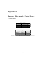
B Energy Electronic Data Sheet Contents
163
C Selected Publications
165
Bibliography
191
List of Figures
1.1
1.2
1.3
1.4
1.5
1.6
Major parts of a sensor node . . . . . . . . . . . . . . . . .
Two examples of environmental sensor network deployments
Telos wireless sensor ‘mote’ . . . . . . . . . . . . . . . . . .
S5 NAP node deployed on an air compressor . . . . . . . . .
Trio wireless sensor node . . . . . . . . . . . . . . . . . . . .
Thesis chapter structure . . . . . . . . . . . . . . . . . . . .
.
.
.
.
.
.
.
.
.
.
.
.
.
.
.
.
.
.
. 1
. 2
. 3
. 5
. 5
. 10
2.1
2.2
2.3
2.4
2.5
2.6
2.7
2.8
2.9
2.10
2.11
2.12
2.13
2.14
2.15
2.16
2.17
2.18
2.19
2.20
2.21
2.22
2.23
2.24
2.25
2.26
2.27
2.28
2.29
2.30
2.31
End-of-life indication for lithium primary batteries . . . . . . . . . .
Comparison of rechargeable battery types . . . . . . . . . . . . . . .
Efficiencies of PV cells relative to STC . . . . . . . . . . . . . . . . .
Comparative efficiency of PV cells . . . . . . . . . . . . . . . . . . .
Characteristics of Schott Solar ASI Indoor Photovoltaic Modules . .
Model of a linear, inertial generator . . . . . . . . . . . . . . . . . .
PMG Perpetuum’s PMG17 vibration harvesting generator . . . . . .
A miniaturised electromagnetic microgenerator . . . . . . . . . . . .
Two-layer bender mounted as a cantilever . . . . . . . . . . . . . . .
The AdaptivEnergy piezoelectric vibration energy harvester . . . . .
Types of electrostatic energy harvester . . . . . . . . . . . . . . . . .
The Micropelt Generic Power Bolt . . . . . . . . . . . . . . . . . . .
Tellurex PG1 Power Generation Kit . . . . . . . . . . . . . . . . . .
Bosch Hydropower generator used with the MPWiNodeX . . . . . .
Wind-powered generators used by wireless sensor nodes . . . . . . .
Intel WISP . . . . . . . . . . . . . . . . . . . . . . . . . . . . . . . .
Midé Volture hybrid energy harvester . . . . . . . . . . . . . . . . .
Conventional and plug-and-play smart sensors . . . . . . . . . . . . .
Star, tree, and mesh network topologies . . . . . . . . . . . . . . . .
Outline of the ZigBee Stack Architecture . . . . . . . . . . . . . . . .
The IDEALS/RMR system diagram . . . . . . . . . . . . . . . . . .
Priority balancing in IDEALS . . . . . . . . . . . . . . . . . . . . . .
The Texas Instruments CC2430EM and eZ430-RF2500 . . . . . . . .
The OSI-BRM, IRM, Foundation Fieldbus H1 and ZigBee stacks . .
Energy management architecture . . . . . . . . . . . . . . . . . . . .
Hardware abstraction architecture implemented in TinyOS 2.0 . . .
The Glacsweb Mk II architecture . . . . . . . . . . . . . . . . . . . .
The Prometheus architecture and prototype . . . . . . . . . . . . . .
Photovoltaic cells ‘harvest’ energy from a ceiling-mounted light unit
The Ambimax architecture and circuitry . . . . . . . . . . . . . . . .
The MPWiNodeX architecture and deployment . . . . . . . . . . . .
.
.
.
.
.
.
.
.
.
.
.
.
.
.
.
.
.
.
.
.
.
.
.
.
.
.
.
.
.
.
.
.
.
.
.
.
.
.
.
.
.
.
.
.
.
.
.
.
.
.
.
.
.
.
.
.
.
.
.
.
.
.
.
.
.
.
.
.
.
.
.
.
.
.
.
.
.
.
.
.
.
.
.
.
.
.
.
.
.
.
.
.
.
xi
.
.
.
.
.
.
.
.
.
.
.
.
.
.
.
.
.
.
.
.
.
.
.
.
14
15
19
19
20
21
22
23
23
24
25
26
27
28
28
30
30
32
36
37
40
41
45
47
48
48
50
51
52
53
54
xii
LIST OF FIGURES
3.1
3.2
3.3
3.4
3.5
3.6
3.7
3.8
3.9
3.10
3.11
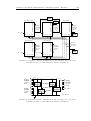
A modular energy subsystem connected to a sensor node .
Conventional and multiplexed 1-wire bus configurations .
Option 1 for multiple energy source combination . . . . .
Option 2 for multiple energy source combination . . . . .
Discharge of a supercapacitor through various loads . . .
Current and power consumption of CC2430EM . . . . . .
Typical discharge profile of Duracell MN1500 alkaline cell
A combined stack . . . . . . . . . . . . . . . . . . . . . . .
A basic template stack . . . . . . . . . . . . . . . . . . . .
An “Energy Stack” . . . . . . . . . . . . . . . . . . . . . .
A “Sensing Stack” . . . . . . . . . . . . . . . . . . . . . .
.
.
.
.
.
.
.
.
.
.
.
.
.
.
.
.
.
.
.
.
.
.
60
66
70
70
75
77
79
81
82
83
85
4.1
4.2
4.3
4.4
4.5
4.6
4.7
4.8
4.9
4.10
4.11
4.12
4.13
4.14
4.15
4.16
4.17
4.18
4.19
Bistable multivibrator . . . . . . . . . . . . . . . . . . . . . . . . . . . .
Undervoltage protection circuit . . . . . . . . . . . . . . . . . . . . . . .
Overvoltage protection circuits . . . . . . . . . . . . . . . . . . . . . . .
Combined undervoltage and overvoltage protection circuit . . . . . . . .
Test of combined undervoltage and overvoltage protection circuit . . . .
Example of voltage measurement circuit . . . . . . . . . . . . . . . . . .
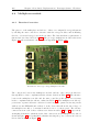
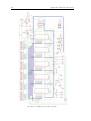
Prototype multiplexer module . . . . . . . . . . . . . . . . . . . . . . . .
Simplified schematic of multiplexer module, showing data connections .
Simplified schematic of multiplexer module, showing power connections
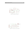
Circuit board for the photovoltaic module . . . . . . . . . . . . . . . . .
The developed PV energy harvesting circuit . . . . . . . . . . . . . . . .
SPICE model for small PV cells . . . . . . . . . . . . . . . . . . . . . . .
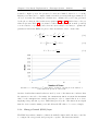
Logarithmic fit of Voc against illuminance . . . . . . . . . . . . . . . . .
Comparison of switching converter against conventional diode . . . . . .
Circuit board for the vibration module . . . . . . . . . . . . . . . . . . .
Circuit board for the mains module . . . . . . . . . . . . . . . . . . . . .
Circuit board for the primary battery module . . . . . . . . . . . . . . .
Circuit board for the supercapacitor module . . . . . . . . . . . . . . . .
Complete system connection . . . . . . . . . . . . . . . . . . . . . . . . .
.
.
.
.
.
.
.
.
.
.
.
.
.
.
.
.
.
.
.
97
98
99
99
100
101
102
103
103
106
108
108
109
111
111
113
114
117
118
5.1
5.2
5.3
5.4
5.5
5.6
5.7
5.8
5.9
SmartRF04EB platform . . . . . . . . . . . . . . . . . . . . .
MSP430F2274 power modes . . . . . . . . . . . . . . . . . . .
Set-up for EEDS on energy module to be programmed . . . .
Oscilloscope trace of reading EEDS on supercapacitor module
A detailed combined stack . . . . . . . . . . . . . . . . . . . .
The SimpliciTI communication stack . . . . . . . . . . . . . .
MSP430 flash write voltage requirements . . . . . . . . . . . .
Calculation of e8 using Taylor expansion . . . . . . . . . . . .
Annotated Hyperterminal output from second test . . . . . .
.
.
.
.
.
.
.
.
.
.
.
.
.
.
.
.
.
.
.
.
.
.
.
.
.
.
.
.
.
.
.
.
.
.
.
.
.
.
.
.
.
.
.
.
.
.
.
.
.
.
.
.
.
.
.
.
.
.
.
.
.
.
.
123
124
126
129
134
135
140
143
148
A.1
A.2
A.3
A.4
A.5
A.6
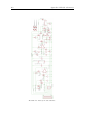
Multiplexer module schematic . .
Photovoltaic module schematic .
Vibration module schematic . . .
Mains module schematic . . . . .
Supercapacitor module schematic
Battery module schematic . . . .
.
.
.
.
.
.
.
.
.
.
.
.
.
.
.
.
.
.
.
.
.
.
.
.
.
.
.
.
.
.
.
.
.
.
.
.
.
.
.
.
.
.
158
159
160
161
161
162
.
.
.
.
.
.
.
.
.
.
.
.
.
.
.
.
.
.
.
.
.
.
.
.
.
.
.
.
.
.
.
.
.
.
.
.
.
.
.
.
.
.
.
.
.
.
.
.
.
.
.
.
.
.
.
.
.
.
.
.
.
.
.
.
.
.
.
.
.
.
.
.
.
.
.
.
.
.
.
.
.
.
.
.
.
.
.
.
.
.
.
.
.
.
.
.
.
.
.
.
.
.
.
.
.
.
.
.
.
.
.
.
.
.
.
.
.
.
.
.
.
.
.
.
.
.
.
.
.
.
.
.
.
.
.
.
.
.
.
.
.
.
.
.
.
.
.
.
.
.
.
.
.
.
.
.
.
.
.
.
.
.
.
.
.
.
.
.
.
.
.
.
.
List of Tables
2.1
2.2
2.3
2.4
2.5
2.6
2.7
Non-rechargeable battery types and characteristics .
Rechargeable battery types and characteristics . . .
Typical indoor and outdoor brightness levels . . . .
List of vibration sources . . . . . . . . . . . . . . . .
Comparison of energy harvesting sources . . . . . . .
Basic TEDS content, as defined in IEEE 1451.4-2004
Thermistor Template Summary . . . . . . . . . . . .
.
.
.
.
.
.
.
.
.
.
.
.
.
.
.
.
.
.
.
.
.
.
.
.
.
.
.
.
13
15
19
21
31
33
34
3.1
3.2
3.3
3.4
3.5
3.6
3.7
3.8
Outline format for the Energy Electronic Data Sheet . . . . . . . . .
Module class codes . . . . . . . . . . . . . . . . . . . . . . . . . . . .
Examples of module type identifiers . . . . . . . . . . . . . . . . . .
Identifiers for modules in the energy subsystem . . . . . . . . . . . .
Common Hardware Interface: microcontroller to multiplexer module
Common Hardware Interface: multiplexer to energy modules . . . .
Energy Priority Levels . . . . . . . . . . . . . . . . . . . . . . . . . .
Simplified discharge of alkaline AA cell . . . . . . . . . . . . . . . . .
.
.
.
.
.
.
.
.
.
.
.
.
.
.
.
.
.
.
.
.
.
.
.
.
64
64
65
67
69
69
75
79
4.1
4.2
4.3
4.4
4.5
4.6
4.7
4.8
4.9
4.10
4.11
Interface pins from multiplexer module (address ‘0’)
Interface pins from multiplexer module (address ‘7’)
Interface pins from photovoltaic module . . . . . . .
Parameters found for Indoor PV Module . . . . . . .
Interface pins from vibration module . . . . . . . . .
Interface pins from wind module . . . . . . . . . . .
Interface pins from thermoelectric module . . . . . .
Interface pins from mains module . . . . . . . . . . .
Interface pins from primary battery module . . . . .
Interface pins from secondary battery module . . . .
Interface pins from supercapacitor module . . . . . .
.
.
.
.
.
.
.
.
.
.
.
.
.
.
.
.
.
.
.
.
.
.
.
.
.
.
.
.
.
.
.
.
.
104
104
106
109
112
112
113
113
115
116
117
5.1
5.2
Electronic Data Sheet for NiMH battery module . . . . . . . . . . . . . . 132
Electronic Data Sheet for photovoltaic module . . . . . . . . . . . . . . . 133
B.1
B.2
B.3
B.4
Electronic
Electronic
Electronic
Electronic
Data
Data
Data
Data
Sheet
Sheet
Sheet
Sheet
for
for
for
for
.
.
.
.
.
.
.
.
.
.
.
.
.
.
.
.
.
.
.
.
.
.
.
.
.
.
.
.
.
.
.
.
.
.
.
.
.
.
.
.
.
.
.
.
.
.
.
.
.
.
.
.
.
.
.
.
.
.
.
.
.
.
.
.
.
.
.
.
.
.
.
.
.
.
.
.
.
.
.
.
.
.
.
.
.
.
.
.
.
.
mains module . . . . . . . . . . . .
vibration energy harvester module .
primary battery module . . . . . .
supercapacitor module . . . . . . .
xiii
.
.
.
.
.
.
.
.
.
.
.
.
.
.
.
.
.
.
.
.
.
.
.
.
.
.
.
.
.
.
.
.
.
.
.
.
.
.
.
.
.
.
.
.
.
.
.
.
.
.
.
.
.
.
.
.
.
.
.
.
.
.
.
.
.
.
.
.
.
.
.
.
.
.
.
.
.
.
.
.
.
.
.
.
.
.
.
.
.
.
.
.
.
163
163
164
164
Listings
5.1
5.2
5.3
5.4
5.5
5.6
5.7
5.8
5.9
Struct for energy module EEDS parameters . . . . . . . . . . . . . .
Measurement types for devices . . . . . . . . . . . . . . . . . . . . .
Struct for multiplexer EEDS parameters . . . . . . . . . . . . . . . .
TParams union for storing module parameters . . . . . . . . . . . .
Parameters to enable energy-awareness for energy modules . . . . . .
Code to interface with Simple Packet Protocol communication stack
Code to interface with SimpliciTI communication stack . . . . . . .
Energy priority enumeration and threshold struct from ECO layer .
Main task loop in shared application layer . . . . . . . . . . . . . . .
xv
.
.
.
.
.
.
.
.
.
.
.
.
.
.
.
.
.
.
.
.
.
.
.
.
.
.
.
130
130
131
131
132
134
135
144
145
Declaration of Authorship
I, Alexander Stewart Weddell, declare that the thesis entitled ‘A Comprehensive Scheme
for Reconfigurable Energy-Aware Wireless Sensor Nodes’ and the work presented in the
thesis are both my own, and have been generated by me as the result of my own original
research. I confirm that:
• this work was done wholly or mainly while in candidature for a research degree at
this University;
• where any part of this thesis has previously been submitted for a degree or any
other qualification at this University or any other institution, this has been clearly
stated;
• where I have consulted the published work of others, this is always clearly attributed;
• where I have quoted from the work of others, the source is always given. With the
exception of such quotations, this thesis is entirely my own work;
• I have acknowledged all main sources of help;
• where the thesis is based on work done by myself jointly with others, I have made
clear exactly what was done by others and what I have contributed myself;
• parts of this work have been published as listed in Section 1.6 of the thesis.
Signed:
Date:
xvii
Acknowledgements
I would like to sincerely thank Nick Harris and Neil White for their technical supervision
and guidance throughout this PhD, and Geoff Merrett for his helpful and thorough
contributions to collaborative work. I would also like to express my appreciation to Neil
Grabham for his contributions in connection with the Adaptive Energy-Aware Sensor
Network (AEASN) project, Bashir Al-Hashimi for his feedback on technical writing, and
to Neil Ross for his analogue circuit design advice. Thanks also to Alex Rogers and Kirk
Martinez for their helpful input as internal examiners over the course of this work.
I also wish to thank the Engineering and Physical Sciences Research Council (EPSRC)
who provided funding to me through a doctoral training award and under Platform grant
EP/D042917/1 ‘New Directions for Intelligent Sensors’, and the Data and Information
Fusion Defence Technology Centre consortium for their financial assistance under the
AEASN project. Thanks also to the School of Electronics and Computer Science for the
provision of excellent research facilities and support.
My gratitude also goes to the other members of the Electronic Systems and Devices
(ESD) group who have made me feel at home (including, but not limited to, Adam
Lewis, Andrew Frood, Cheryl Metcalf, Dirk de Jager, Evangelos Mazomenos, Matthew
Swabey, Mustafa Imran Ali and Russel Torah). Special thanks must go to my parents
for their love, support and encouragement over many years. Finally, I would like to
thank my wife, Jenny, for her love, understanding, and unwavering confidence in me.
xix
To Jenny, with all my love.
xxi
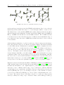
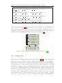
Nomenclature
α
Ratio between resistors in voltage divider arrangement
αψ
Voltage factor
ατ
Temperature factor
A
Cross-sectional area [m2 ]
C
Capacitance [F]
cT
Damping coefficient
d
Separation distance [m]
η
Carnot efficiency
0
Permittivity of free space
E
Energy [J]
EV
Illuminance [Lx]
I
Current [A]
I0
Diode saturation current [A]
Impp
Maximum power point current [A]
Iph
Photogenerated current [A]
Isc
Short-circuit current [A]
k
Spring constant
k
Thermal conductivity of material [W K −1 m−1 ]
k
Voltage ratio for photovoltaic cells
kB
Boltzmann constant
l
Length [m]
λ
Wavelength of transmission [m]
m
Mass of oscillating object [kg]
m
Current ratio for photovoltaic cells
ν
Velocity of fluid [ms−1 ]
P
Power [W]
P0
Inital transmitted power [W]
ϕt
Remaining lifetime fraction
ϕE
Energy fraction
ϕL
Logarithmic discharge fraction
ϕV
Voltage fraction
q
Electronic charge [C]
xxiii
xxiv
NOMENCLATURE
q0
Heat flow through material [W/m2 ]
ρ
Density of fluid [kg/m3 ]
r
Radius of transmission [m]
R
Resistance [Ω]
t
Expected lifetime
tγ
Guaranteed lifetime
T
Temperature [K]
Thigh
‘Hot’ side temperature [K]
Tlow
‘Cold’ side temperature [K]
T
Expected temperature [K]
Tρ
Rated temperature [K]
V
Voltage [V]
V0
Starting voltage [V]
Vmpp
Maximum power point voltage [V]
Voc
Open-circuit voltage [V]
Vstart
Initial voltage applied [V]
Vmax
Maximum voltage reached [V]
w
Width [m]
y
Input displacement [m]
z
Spring displacement [m]
Abbreviations
µC
Microcontroller
ADC Analogue-to-Digital Converter
AEASN Adaptive Energy-Aware Sensor Networks
AM1.5 Air Mass 1.5
AMR Automatic Meter Reading
ANSI American National Standards Institute
ASI
Amorphous Silicon
CEDS Component Electronic Data Sheet
CENS Center for Embedded Networked Sensing
CHI
Common Hardware Interface
DIF
Data Information Fusion
DTC Defence Technology Centre
EAN Energy Analysis Layer
ECO Energy Control Layer
EEDS Energy Electronic Data Sheet
EMA Energy Management Architecture
EP
Energy Priority
EPROM Electrically Programmable ROM
EPSRC Engineering and Physical Sciences Research Council
ESD
Electronic Systems and Devices
GPS
Global Positioning System
xxv
xxvi
ABBREVIATIONS
HAL Hardware Adaptation/Abstraction Layer
HEDS Health Electronic Data Sheet
HeH
Hybrid Energy Harvester
HIL
Hardware Interface Layer
HPL
Hardware Presentation Layer
HVAC Heating, Ventilation and Air Conditioning
I/O
Input/Output
IDEALS Information manageD Energy aware ALgorithm for Sensor networks
IEEE Institute of Electrical and Electronics Engineers
IrDA Infrared Data Association
ISA
International Society of Automation
ISM
Industrial, Scientific and Medical
KTN Knowledge Transfer Network
LAN Local Area Network
LPM Low-Power Mode
MIT
Massachusetts Institute of Technology
NiCd Nickel Cadmium
NiMH Nickel Metal Hydride
PC
Personal Computer
PCB Printed Circuit Board
PMBus Power Management Bus
PP
Packet Priority
PRIMP Priority-Based Multi-Path Routing Protocol
PV
Photovoltaic
PYE Physical Energy Layer
PYS
Physical Sensing Layer
QoS
Quality of Service
ABBREVIATIONS
RAM Random Access Memory
RF
Radio Frequency
RF-ID Radio Frequency Identification
RMR Rule Managed Reporting
ROM Read-Only Memory
SBD
Smart Battery Data
SEV
Sensor Evaluation Layer
SMBus System Management Bus
SoC
System-on-Chip
SPR
Sensor Processing Layer
STC
Standard Test Conditions
TEDS Transducer Electronic Data Sheet
TI
Texas Instruments
UHF Ultra High-Frequency
WISP Wireless Identification and Sensing Platform
WLAN Wireless LAN
WPAN Wireless Personal Area Network
xxvii
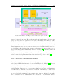
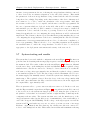
Chapter 1
Introduction
1.1
Wireless autonomous sensing
“The powering of remote and wireless sensors is widely cited
as a critical barrier limiting the uptake of this technology.”
Energy Harvesting Technologies to Enable Remote and Wireless Sensing,
Sensors and Instrumentation KTN Technical Report [1].
Remote and wireless sensors, referred to hereafter as ‘wireless autonomous sensors’ or
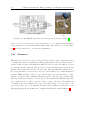
‘wireless sensor nodes’, offer the facility to remotely monitor parameters such as temperature, pressure, and vibration, in machines, buildings, or the environment. These
nodes will typically feature at least one type of sensor, a microcontroller (to manage
and process data), a wireless communication interface (which is almost always radio
frequency (RF) based), and a power supply (conventionally a battery, but potentially
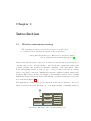
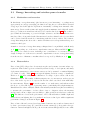
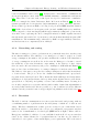
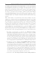
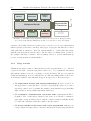
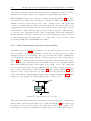
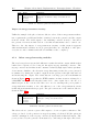
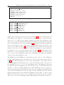
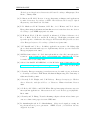
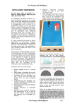
harnessing energy harvested from the environment). A typical architecture for a sensor
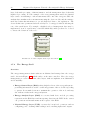
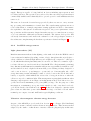
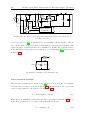
node is shown in Figure 1.1.
The applications of this technology are extremely varied but key drivers for the popularity of wireless sensors are the high cost, or the impracticality, of installing wiring for
Comms
Interface
Processor
Sensing
Hardware
Sensor
Interface
Memory
Energy
Resources
Energy
Management
MCU
I/O & ADC
Clocks
Figure 1.1: The major parts of a wireless sensor node.
1
2
Chapter 1 Introduction
conventional sensors. Wireless technology allows parameters to be monitored, or experiments to be carried out, which would previously have been prohibitively expensive or
time-consuming. Furthermore, in contrast to conventional data-logging equipment, wireless sensors on remote long-term deployments permit parameters to be monitored with
a high temporal resolution and provide a real-time, or near-real-time, representation of
the situation.
Wireless sensing technology enables devices to be deployed quickly and easily by way
of the fact that they are able to self-configure without the need for a fixed layout or
infrastructure. State-of-the-art communication protocols allow sensor nodes to form
mesh networks and work together to route information to a central point. Normally,
nodes operate with a low duty cycle to conserve energy (consuming tiny levels of power
while asleep), and utilise low-power communications which minimises their active energy
consumption. This means that their average power requirement is very low and allows
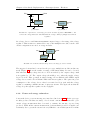
them to deliver operational lifetimes that are typically measured in months or years.
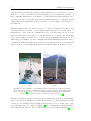
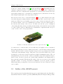
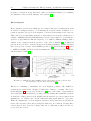
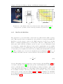
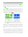
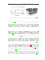
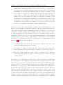
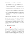
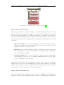
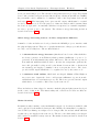
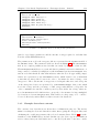
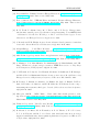
(a) Glacsweb base station
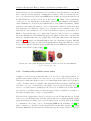
(b) Active volcano monitoring
Figure 1.2: Two examples of environmental sensor network deployments: (a) a Glacsweb base station is used to communicate with nodes buried deep in a Norwegian glacier
(reproduced from [2]), and (b) a node performing seismic and infrasonic measurements
on the side of an active volcano in Ecuador (reproduced from [3]).
Examples of real deployments of wireless sensor systems range from the relatively mundane to the extreme. Machinery condition monitoring is a popular application for this
technology. For example, BP have utilised wireless sensor nodes to monitor the condition of machinery in one of their oil tankers [4]. More challenging applications include
embedding wireless sensor nodes deep inside glaciers to monitor their dynamics [2], or on
Chapter 1 Introduction
3
volcanoes to monitor seismic events [3] (as shown in Figure 1.2). Essentially, these are
examples of applications where conventional sensing would be expensive or impractical,
and where the lower complexity and deployment cost of wireless autonomous sensor systems enables parameters to be measured for a sustained period, and monitored remotely,
with a higher spatial (and often temporal) resolution.
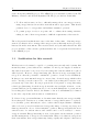
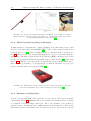
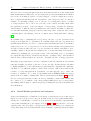
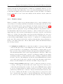
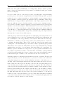
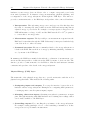
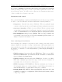
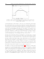
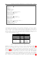
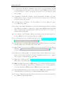
The Crossbow Telos ‘mote’, as shown in Figure 1.3, is a popular wireless sensor platform that integrates sensing hardware with a low-power microcontroller and a radio
transceiver. This device is normally powered by a pair of AA non-rechargeable batteries, and the lifetime of the node is ultimately dependent on the the characteristics of
the batteries and activity of the node (i.e. its duty cycle and the power consumption
of its sensing hardware when performing measurements). Obviously the batteries must
be replaced when depleted, which imposes a maintenance requirement that can prove
costly over the course of long deployments.
Figure 1.3: The Telos wireless sensor ‘mote’ (reproduced from [5]).
A common facet of wireless sensor nodes is that they are highly resource-constrained.
They will typically have an 8-bit or limited 16-bit microcontroller with a relatively small
amount of memory, and be restricted by their energy resources (operating from batteries
or harvested environmental energy). They have low-power radios which often operate
in relatively crowded radio frequencies and have a limited transmission range. The cost
and physical size of devices are also common constraints, as are their weight and deployment location. For these reasons, the careful design, installation, and management of
these systems is essential. This thesis will consider only low-power sensor devices which
typically consume, on average, less than one milliwatt of power in general operation,
which means that powering these devices from relatively low levels of harvested energy
can be feasible.
1.2
Outline of the AEASN project
The research presented in this thesis has in part been undertaken under the Data Information Fusion Defence Technology Centre (DIF DTC) Phase II ‘Adaptive Energy-Aware
4
Chapter 1 Introduction
Sensor Networks’ (AEASN) project. The AEASN project was funded jointly by the UK
Ministry of Defence and General Dynamics UK. The project had two main aims:
1. To allow wireless sensor nodes to efficiently manage their own energy resources,
using energy harvested from their environment where appropriate. This should
permit nodes to be energy-aware and facilitate sustained operation.
2. To permit groups of nodes to negotiate and co-ordinate their sensing activities,
taking account of their energy status, to fulfil the requirements of the network.
The work presented in this thesis focuses on the first of these aims – delivering energyaware nodes that are able to manage their energy resources efficiently and accept energy
harvested from the environment. The research carried out by the author has fed into this
project, and three of his conference publications have also been presented as deliverables
of the AEASN project.
1.3
Justification for this research
Wireless sensor nodes must be capable of operating autonomously, and for many this
means they must operate without the constraint of a wired power supply. Conventionally, such devices have been powered by non-rechargeable batteries which are replaced
when depleted. However, energy harvesting (also known as energy scavenging) technology now offers the potential to sustain the operation of sensor nodes indefinitely.
In this process, environmental energy is converted into electrical energy which is then
used to directly power the sensor node, or is buffered (in rechargeable batteries or supercapacitors) for use later. Recent progress in the development of energy harvesting
technologies (harvesting electrical energy from such sources as light, vibration, or temperature difference) now permits sensors to be free from the limitations of operation from
non-rechargeable batteries. Indeed, the lifetime of the node will ultimately be limited
by its other components, such as sensors or flash memory.
To deliver a long operational lifetime, nodes must ensure that they use energy carefully.
Non-rechargeable batteries store a finite amount of energy which cannot be replaced,
so nodes must operate efficiently in order to achieve their designed lifetime. Similarly,
where nodes are powered from harvested energy they must, on average, use less power
than is generated in order to deliver sustained operation. Energy is arguably the most
critical resource for wireless sensors, and careful control of node activity to conserve
energy is essential. Energy harvesting is often, by its nature, an inconsistent operation
and the management of energy is a non-trivial task. Where nodes harvest energy from
their environment, their energy status may change rapidly and adaptive behaviour is
Chapter 1 Introduction
5
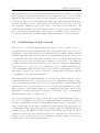
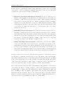
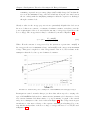
desirable. In addition, seemingly straightforward operations such as assessing the stateof-charge of certain energy storage devices can be difficult. The real-time assessment of
the energy status of a sensor node can therefore be a highly complex task.
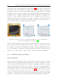
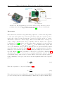
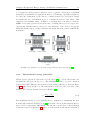
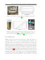
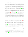
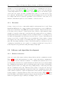
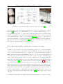
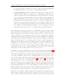
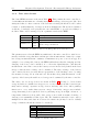
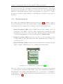
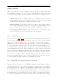
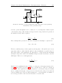
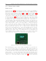
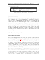
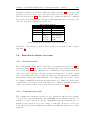
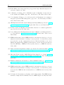
Figure 1.4: A S5 NAP vibration powered sensor node mounted on an air compressor
during a trial (reproduced from [6]).
Figure 1.5: Trio wireless sensor node and its key components (reproduced from [7]).
At present, systems incorporating energy harvesting (such as the S5 NAP vibrationpowered node shown in Figure 1.4, and the Trio outdoor solar-powered node shown in
Figure 1.5) are designed for specific harvesting devices and are relatively inflexible. The
re-configuration of the device to interface with an alternative energy harvesting device
would require a re-design of the node’s hardware and embedded software. Furthermore,
there are very few nodes which allow the combination of multiple energy harvesting
devices. To the best of the author’s knowledge, there are no systems that allow the
selection of appropriate energy hardware at the time of deployment (or, indeed, allow it
to be changed after deployment). It may be argued that this is a major limiting factor
for the applicability of wireless sensor nodes able to operate from environmental energy.
6
Chapter 1 Introduction
The justification for the work presented in this thesis is the development of reconfigurable, efficient, energy-aware wireless sensor nodes which are able to overcome these
limitations. There is a need for devices to have a flexible energy subsystem that can accommodate a range of devices including energy harvesters, buffers, and non-rechargeable
batteries. Information on the energy status of the system can be provided to the software application running on the node in order to control the node’s activity level. As
outlined in the following section, the scheme is verified on a sensor node in a challenging
indoor environment, allowing energy components to be exchanged and for the node to
recognise and handle these hardware changes, and remain aware of its energy status.
1.4
Contributions of this research
The scheme proposed in this thesis permits the energy resources of a sensor node to be
configured in-situ by system installers at the time of deployment, and for the node to automatically recognise and manage its energy subsystem. For example, when the system
is installed the appropriate types and sizes of energy harvesting and storage devices can
be chosen and connected to the system. On first power-on, or indeed afterwards when
a change is detected, the node interrogates a memory on each device to determine its
operating parameters and other information. The introduced scheme permits multiple
energy devices to be connected to a node, with the node able to address and manage each
device individually. This represents a major step forward for the application of energy
harvesting for sensor nodes, as nodes can now be efficient and energy-aware without
being limited to a specific energy subsystem.
The scheme includes the implementation of a new embedded software structure, a novel
common hardware interface to allow the sensor node to communicate with its reconfigurable energy subsystem, and a new ‘energy electronic data sheet’ format which allows
data on parts of the energy subsystem to be stored on the modules themselves. Together,
this represents a comprehensive scheme for reconfigurable energy-aware sensor nodes.
This scheme is validated through the application of the methodology to a challenging
application using a range of energy devices.
A prototype system has been deployed in an indoor environment, harvesting energy of
the order of one milliwatt. It was developed under this scheme to sustain its operation,
and has a plug-and-play energy subsystem which allows its energy components to be
swapped at the time of deployment, or during its operation. In the deployment, the node
is demonstrated with energy harvested from vibration, light, and thermal differences,
with the energy being buffered in supercapacitors and rechargeable batteries. A nonrechargeable battery provides a last-ditch back-up for emergency use. The system is
shown to operate from a range of devices, which are swappable during operation, and
remains aware of its energy status throughout.
Chapter 1 Introduction
7
In line with the requirements detailed earlier, this thesis describes the development
of processes to deliver reconfigurable, efficient, energy-aware sensor nodes. The main
contributions of the research can thus be summarised:
1. Electronic data sheets and hardware interfaces: in order to deliver a reconfigurable ‘plug-and-play’ energy subsystem for wireless sensor nodes, it has been
necessary to define an electronic data sheet format so that operating parameters
can be stored on energy-related devices. This is a progression from the established
‘transducer electronic data sheet’ concept. A common hardware interface, which
standardises the interface between the sensor node and its sensor hardware, has
been developed to enable this data sheet to be read and allow the node’s energy
status to be monitored.
2. Embedded software development: an embedded software structure has been
implemented which splits energy and sensor management tasks from the communications stack into their own separate software stacks. The energy stack interfaces
with the energy hardware, including the electronic data sheets, through the hardware interface. It allows the application running on the sensor node to adapt its
behaviour dependent on the amount of available energy.
3. Energy harvesting and management: circuits have been developed to manage
energy from harvesting devices and batteries. Algorithms and circuits for the
management of energy resources and determination of power status have also been
developed. The dynamics of energy harvesting and storage devices have been
characterised and implemented in the deployed system, with operating information
being stored in the electronic data sheets and used by the embedded software.
Brought together, the work described in this thesis represents a comprehensive scheme
for delivering reconfigurable wireless sensor nodes. The scheme defines the hardware
and software interfaces between components, and provides a plug-and-play capability
for the energy subsystems of nodes. The work has been verified through the deployment
of the system in a demonstrator with a range of swappable energy components, and
sensor node platforms, which are able to interface with the energy hardware.
The overall evaluation of the system is both quantitative and qualitative. Some parameters, such as the impact of adding circuitry to deliver energy-awareness, is relatively
straightforward to evaluate; as is the additional processing overhead due to carry out
these calculations. The net benefit to the system is in delivering energy-awareness
through an integrated system. The process of developing and of deploying a system
which is compliant with this scheme is explored and the benefits and drawbacks are
expressed in terms of programming effort and ease of deployment.
8
Chapter 1 Introduction
1.5
What is ‘reconfigurability’ ?
In the context of this thesis, ‘reconfigurability’ refers to the ability:
1. To select energy resources, as appropriate to the deployment environment, and
connect them together at the time the system is installed.
2. To enable the energy resources to be exchanged while the system is operational,
and for the system to recognise and adapt to these changes.
3. To realise these changes ‘in the field’ without access to specialist equipment:
i.e. without needing to change the microcontroller’s embedded software.
These capabilities mean that it is possible to set up the energy hardware on the device
as appropriate to the environmental conditions, and to be able to reconfigure the energy
hardware on the device without disrupting its operation. The reconfigurable system
described in this thesis enables the system to remain energy-aware and manage its
operation, regardless of the hardware used to power the device.
1.6
Publications
The following journal and conference papers have been produced as a result of the work
carried out under this project:
1. Weddell, A. S., Harris, N. R. and White, N. M. (2008) “Alternative Energy Sources
for Sensor Nodes: Rationalized Design for Long-Term Deployment”. In: International Instrumentation and Measurement Technology Conference, May 12-15,
2008, Victoria, British Columbia, Canada.
2. Weddell, A. S., Harris, N. R. and White, N. M. (2008) “An Efficient Indoor Photovoltaic Power Harvesting System for Energy-Aware Wireless Sensor Nodes”. In:
Eurosensors 2008, 7-11 September 2008, Dresden, Germany.
3. Merrett, G. V., Weddell, A. S., Lewis, A. P., Harris, N. R., Al-Hashimi, B. M. and
White, N. M. (2008) “An Empirical Energy Model for Supercapacitor Powered
Wireless Sensor Nodes”. In: 17th International IEEE Conference on Computer
Communications and Networks, 3-7 August 2008, St Thomas, Virgin Islands (USA).
4. Weddell, A. S., Merrett, G. V., Harris, N. R. and Al-Hashimi, B. M. (2008) “Energy
Harvesting and Management for Wireless Autonomous Sensors”. Measurement +
Control, 41 (4). pp. 104-108. ISSN 0020-2940
Chapter 1 Introduction
9
5. Weddell, A. S., Grabham, N. J., Harris, N. R. and White, N. M. (2008) “Flexible
Integration of Alternative Energy Sources for Autonomous Sensing”. In: Electronics System-Integration Technology Conference, September 1-4, 2008, Greenwich,
UK.
6. Merrett, G. V., Weddell, A. S., Harris, N. R., Al-Hashimi, B. M. and White,
N. M. (2008) “A Structured Hardware/Software Architecture for Embedded Sensor
Nodes.” In: 17th International Conference on Computer Communications and
Networks, 3-7 August 2008, St Thomas, Virgin Islands (USA).
7. Merrett, G. V., Weddell, A. S., Berti, L., Harris, N. R., White, N. M. and AlHashimi, B. M. (2008) “A Wireless Sensor Network for Cleanroom Monitoring”.
In: Eurosensors 2008, 7-11 September 2008, Dresden, Germany.
8. Weddell, A. S., Grabham, N. J., Harris, N. R. and White, N. M. (2009) Modular
Plug-and-Play Power Resources for Energy-Aware Wireless Sensor Nodes. In:
Sixth Annual IEEE Communications Society Conference on Sensor, Mesh and Ad
Hoc Communications and Networks - SECON 2009, 22-26 June 2009, Rome, Italy.
A selection of these papers may be found in Appendix C. The author of this thesis
has also co-authored a chapter entitled “Wireless Devices and Sensor Networks” for the
book “Energy Harvesting for Autonomous Systems” (edited by Beeby, S. P., and White,
N. M.) which is to be published by Artech House, London, in July 2010.
1.7
Document structure
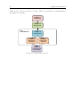
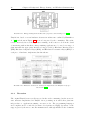
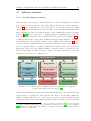
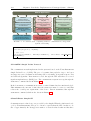
The overall structure of this thesis is shown in Figure 1.6. Chapter 2 introduces the
basis for the operation of sensor nodes: energy, sensing, and communications. It covers
the available technologies for energy storage and generation, and how to monitor these
resources. Intelligent sensing standards are also discussed, along with wireless transmission protocols relevant to sensing. It then looks at the current state-of-the-art in sensor
nodes and existing systems operating from harvested energy. Later chapters present the
fundamental work carried out in line with the aims of the project, along with description of practical developments including a demonstration system. Chapter 3 describes
the design of a wireless sensor node as a reconfigurable system. The chapter covers the
overall design of the system for reconfigurability, including the development of an energy
electronic data sheet, common hardware interface, and algorithms for energy management. General structures for the system’s energy subsystem and its embedded software
are also introduced. The development of prototype system hardware is described in
detail in Chapter 4, with a discussion of the overall system design along with detailed
consideration of each module developed. The embedded software implementation for the
system is documented and evaluated in Chapter 5. This thesis concludes in Chapter 6
10
Chapter 1 Introduction
with a review of the work carried out and considers opportunities for standardisation
and future development.
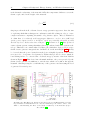
Chapter 1
Introduction
Chapter 2
Background
Key
Contributions
Chapter 3
Development
Chapter 4
Case Study:
Hardware
Chapter 5
Case Study:
Software
Chapter 6
Conclusions &
Future Work
Figure 1.6: Thesis chapter structure.
Chapter 2
Background: Energy, Sensing,
and Wireless Communication
2.1
Introduction
This chapter gives an overview of the technologies related to this project, and the current
state-of-the-art in energy harvesting wireless sensor nodes. The energy devices covered
are appropriate for milliwatt-scale sensor nodes, so large-scale energy generation and
storage technologies (such as those used to augment or replace a mains electricity supply for high-power devices) are not covered. Technologies related to energy storage
are introduced in Section 2.2, and energy harvesting and wireless power transfer technologies are discussed in Section 2.3. Standards and methods for intelligent sensing,
including plug-and-play sensors and transducer electronic data sheets, are introduced
in Section 2.4. Section 2.5 introduces wireless transmission protocols used by wireless
sensor networks, and strategies for energy-aware operation are discussed in Section 2.6.
Wireless sensor nodes and their underlying components are introduced in Section 2.7,
and Section 2.8 discusses software and algorithm development. A range of sensor node
deployments, including energy harvesting systems and a limited number of prototypes
that support multiple energy devices, are introduced in Section 2.9.
2.2
2.2.1
Energy storage
Motivations and overview
As discussed in Chapter 1, wireless sensor nodes will normally operate from non-rechargeable batteries or (less commonly) energy harvested from their environment. The
low rate of power generation from most energy harvesting devices means that they
11
12
Chapter 2 Background: Energy, Sensing, and Wireless Communication
are generally unable to directly power nodes in their active mode, so it is normally
necessary to ‘buffer’ energy to accommodate the periodic large bursts of current draw
caused by duty-cycled operation (i.e. when the node becomes active after a period of
‘sleep’). Electrical energy may also be stored for longer periods, for example overnight,
to compensate for periods where energy cannot be generated. The buffering of energy
is normally achieved by using rechargeable batteries, supercapacitors, or a combination
of the two.
This section reviews a selection of popular battery and supercapacitor technologies, their
characteristics, and considerations for their use with wireless sensors. Some alternative
methods of energy storage are also considered, and the section concludes with a comparison between commercially-available energy storage devices considering factors such
as energy density, leakage power, and cost.
2.2.2
Non-rechargeable (primary) batteries
Non-rechargeable (otherwise known as ‘primary’) batteries are by far the most prevalent
technology for powering wireless sensor nodes, as they are relatively cheap and offer a
high energy density compared to rechargeable batteries or supercapacitors. The batteries
are either replaced when depleted, or the node is deployed with a battery which will last
for the system’s entire operational lifetime. In the field of low-power wireless sensor
networks, two primary battery chemistries have achieved dominance:
1. In short-term deployments, or where sensor nodes are accessible and batteries can
be changed without causing major disruption, alkaline (typically alkaline manganese dioxide, or similar) cells are most frequently used. This chemistry has a
low self-discharge rate and hence a shelf-life of several years. This chemistry is
very popular for use in consumer electronics devices, which means that its cost is
relatively low.
2. For long-term deployments, where nodes may be inaccessible and battery replacement impractical or expensive, long-life lithium primary cells are generally used
(typically lithium thionyl chloride LiSOCl2 ). These have a very low self-discharge
rate, and a higher specific energy and energy density than alkaline chemistries.
These cells can have an operational life in excess of ten years, but are relatively
expensive.
Detailed parameters for these battery types, along with information on other popular
chemistries, are shown in Table 2.1. The nature of wireless sensor network deployments
means that long lifetimes are desirable; otherwise the costs of regularly changing batteries could outweigh the savings made through not having to install cabling to sensors.
The bursty characteristic of current draw by wireless sensor nodes when sensing and
Chapter 2 Background: Energy, Sensing, and Wireless Communication
13
communicating must be supported by the battery without resulting in excessive voltage depression. These requirements rule out some common battery types, such as zinc
carbon and smaller lithium coin cells, from use in this application.
Specific energy [Wh/kg]a,b
Energy density [Wh/L]
a,b
Zinc
Carbon
Alkaline
Lithium
Manganese
Dioxide
Lithium
Thionyl
Chloride
85
145
380
230
165
400
715
535
Nominal voltage [V]
1.5
1.5
3.6
3.0
Open-circuit voltage [V]a
1.6
1.5-1.6
3.65
3.3
1.25-1.1
1.25-1.15
3.6-3.3
3.0-2.7
0.9
0.9
3.0
2.0
Midpoint voltage [V]
a,c
End voltage [V]
Self-discharge [%/year]
a,d
7
4
1-2
1-2
Operating T [◦ C]
-10 to 50
-20 to 55
-60 to 85
-20 to 55
Discharge profile
Sloping
Mod. slope
Flat
Flat
Status
High production, decreasing popularity
Most popular
primary battery
Mainly
for
special applications
Increasing
consumer
production
Advantages
Low cost
High capacity; good lowT
low-rate
performance
High E density, long shelf
life
High E density, good lowT high-rate
Limitations
High gassing
rate,
poor
performance
Moderate cost
but best at
high rates
Voltage delay
after storage
Limited sizes
and shipping
a
b
c
d
At 20◦ C.
For cylindrical cell.
For favourable discharge conditions.
Normally decreases with time of storage.
Table 2.1: Non-rechargeable battery types and characteristics (adapted from [8]).
One of the longest documented deployments of a wireless sensor – an Automatic Meter
Reading (AMR) system for a water meter which has been operating for over 20 years
– is powered by a Tadiran lithium primary cell [9]. The fact that lithium cells have
been demonstrated operating for very long periods of time is a welcome verification
of the application of this technology to long-term wireless sensing applications. An
arguable drawback of these cells, however, can be their flat discharge profile. As shown
in Figure 2.1, end-of-life for these lithium cells can only be detected passively up to 3%
before cut-off (or actively, by applying a pulsed load to the cell, up to 15% before cutoff). In a deployment of ten years, this 3% warning corresponds to approximately three
months, or a 15% indication is equivalent to 18 months. Providing that the sensor node
draws the expected amount of current, this in itself is not problematic (three months is, in
most applications, an acceptable amount of time to arrange battery replacement). In the
case of a malfunctioning sensor that is drawing a substantial amount more current than
expected, however, the warning period would clearly be much shorter. The difficulty of
14
Chapter 2 Background: Energy, Sensing, and Wireless Communication
identifying the end-of-life or state-of-charge of primary batteries is a major drawback for
their application in wireless sensor nodes. Primary batteries are resources that cannot
be used after they have been expended (except for some negligible recovery effects);
therefore, energy must be used conservatively at all times (to compensate for the poor
resolution of energy-awareness) in order to ensure that desired system lifetimes can be
achieved.
Figure 2.1: End-of-life indication for lithium primary batteries. The grey curve shows
seasonal temperature cycles, the solid curve shows discharge on continuous load at
+25◦ C, and the dashed curve shows the trend of test pulses (reproduced from Tadiran
technical brochure [10]).
2.2.3
Rechargeable (secondary) batteries
Some of the most frequently-used rechargeable (also known as ‘secondary’) battery
chemistries in wireless sensor network applications are lithium-ion, lithium-polymer,
and nickel metal hydride. Figure 2.2 shows a comparison of the energy densities of
rechargeable battery types; the battery capacity values quoted in data sheets, however,
only give part of the story. The amount of energy that can be provided by a battery is
highly dependent on the methods of charge and discharge, and the conditions in which
it is kept [11]. For example, lithium-ion cells are highly sensitive to overcharge and undercharge, and thus protection circuitry must be built in. Different battery chemistries
require other charging methods: lithium-ion batteries require a constant charging current until they have reached 90% capacity, followed by a constant voltage. NiMH and
NiCd batteries prefer a constant current throughout the recharge process [12].
With modern cell constructions, memory effects are now negligible. NiCd cells have
historically been most susceptible to this effect, but the Handbook of Batteries states
that “most users may never experience low performance due to memory effect . . . the use
of the term ‘memory effect’ persists, since it is often used to explain low battery capacity
that is attributable to other problems” [8]. The number of cycles that the battery can
go through is dependent on its chemistry and other factors, but modern cells generally
Chapter 2 Background: Energy, Sensing, and Wireless Communication
15
Figure 2.2: Comparison of rechargeable battery types in terms of volumetric and
gravimetric energy densities (reproduced from Tarascon and Armand [13]).
have a lifetime of at least a few hundred cycles. Another parameter (rarely quoted, but
important to energy-harvesting nodes) is the ‘coulometric efficiency’. This indicates the
proportion of energy stored against the energy expended in charging. A figure of 99.9%
is typical for lithium-ion cells, but is somewhat lower for other battery chemistries (and
highly dependent on charging conditions) [8]. Some typical parameters for the most
commonly-used secondary battery types are shown in Table 2.2.
Lead acid
NiCd
NiMH
Lithium
Specific energy [Wh/kg]
30
35
75
150
Energy density [Wh/L]
90
100
240
400
Nominal voltage [V]
2.0
1.2
1.2
4.0
Open-circuit voltage [V]
2.1
1.29
1.4
4.1
Operating voltage [V]
2.0-1.8
1.25-1.00
1.25-1.10
4.0-3.0
End voltage [V]
1.75
1.0
1.0
3.0
Self discharge [%/month]
4-8
15-20
15-25
2
Calendar life [years]
2-8
2-5
2-5
?
Cycle life [cycles]
250-500
300-700
300-600
1000+
Discharge profile
Flat
Very flat
Flat
Advantages
Long
life
on float, Tindependent
Good low-T
high-rate
High
density
Limitations
Can’t
store
discharged,
low cycle life
Memory effect
Moderate cost
a
Sloping
E-
High
density
Low rate
At room temperature 25◦ C.
Table 2.2: Rechargeable battery types and characteristics (adapted from [8])
E-
16
2.2.4
Chapter 2 Background: Energy, Sensing, and Wireless Communication
Supercapacitors
Supercapacitors (also known as ultracapacitors, electrochemical capacitors, or electric
double-layer capacitors) offer a much higher energy density than aluminium electrolytic
capacitors, but retain many of their other characteristics. Unlike conventional capacitors (which have two ‘plates’ separated by a dielectric), supercapacitors have two layers
of the same substrate (typically activated carbon) which store charge, separated by a
very thin material. Their operation is more complex than conventional capacitors (but
they loosely follow the standard capacitor equation), and due to their thin insulator
they will typically have a lower operating voltage. They are relatively insensitive to
charge/discharge cycling and require no special charging circuitry [14]. However, their
energy density remains an order of magnitude below those of conventional secondary
batteries and their leakage (or self-discharge) rates are also relatively high. Supercapacitors have been incorporated into self-powered sensing systems where they provide
a cache between harvesting sources, a secondary battery, and a sensor node. Jiang et
al. [15] carried out experiments to determine the self-discharge rates of a number of supercapacitors, and found that the worst-performing supercapacitor lost approximately
50% of its energy through leakage in 16 hours, and that the capacitor size does not give
an indication of likely self-discharge rate. There is, however, some doubt over whether
the observed effects were attributable to leakage, or the redistribution of charge within
the supercapacitor.
A common range of supercapacitors is the Panasonic Gold series: their technical guide
[16] has information on the modelling and behaviour of supercapacitors. Wireless sensor
nodes, such as the those described in Section 2.7.1, draw around 30mA when fully active
and communicating (excluding the current draw of any additional sensors or peripherals). The Panasonic HW series has a maximum operating voltage of 2.3V, maximum
operating temperature of 70◦C, and guaranteed lifetime of 1,000 hours [16]. Continued developments in supercapacitor technology are improving their characteristics. For
example, the CAP-XX range of supercapacitors have thin prismatic packages, low selfdischarge currents and are able to sustain high levels of peak current. For example, the
HS208 model [17] has a typical leakage current of 1.0µA after being charged for 72 hours
and can tolerate a comparatively high peak current of 20A.
2.2.5
Other energy storage mechanisms
Some alternative energy storage technologies exist. For example, fuel cells have been
forecast to be a high-capacity replacement for batteries; however, current research indicates that, due to constraints on size and the requirement for precision machining, micro
fuel cells are unlikely to offer substantially higher energy densities than primary batteries
[18]. Even where electrodes can be microfabricated, the task of microfabricating the fuel
Chapter 2 Background: Energy, Sensing, and Wireless Communication
17
reservoir and plumbing is substantial. Fuel cells, however, offer higher power densities
and therefore may be of use in sensor nodes with a high current requirement. Some
research micro-fuel cells have been demonstrated with success, including a fuel system
providing 25mA from a thin-film cell with an area of 2cm2 [19]. Alternatively, advances
in micromachining have opened up the possibility of creating micro-heat engines to produce electrical power from hydrocarbon fuels. There are a number of possible approaches
to design of the heat engine, including piston-based combustion engines, Wankel internal
combustion engines, and micro gas turbine engines. The P3 micro heat engine makes use
of thermal expansion to generate electrical power by means of a piezoelectric material
[20]. Conversely, radioactive sources could potentially offer massive energy densities –
for example, the
63 Ni
isotope has been used by Li and Lal [21] to actuate a conductive
cantilever. Beta particles emitted from the isotope collect on the cantilever, which effects an electrostatic attraction, eventually causing the cantilever to contact the isotope
and discharge, and the process restarts. Along similar lines, Fleurial [22] presents a survey of technologies, including the combination of Radioactive Heat Units (RHUs) with
thermoelectric generators.
2.2.6
Discussion
This section has covered the available technologies for energy storage, focussing on primary and secondary batteries and supercapacitors (with some additional consideration
of other energy storage mechanisms). In summary, primary batteries have the advantage
that they have a high energy density, long shelf-life, and relatively low cost; however,
they are a limited resource that must be replaced when expended. Some of the long-life
technologies also have a stable discharge characteristic which limits the resolution of
state-of-charge determination or end-of-life identification. Conversely, secondary batteries can be recharged, and offer broadly similar energy densities to those of primary
batteries; however, they are sensitive to the number of charge/discharge cycles to which
they are exposed, and must be charged in a controlled manner to maximise their lifetime. Finally, supercapacitors offer an energy density which is approximately an order
of magnitude lower than those of batteries, exhibit capacitor-like behaviour, and are
relatively insensitive to the method of charge or discharge. The choice of energy storage
technology is highly dependent on the other considerations for the energy subsystem of
the sensor node but, due to their favourable characteristics, supercapacitors are most
commonly used in systems which feature energy harvesting technology.
18
2.3
2.3.1
Chapter 2 Background: Energy, Sensing, and Wireless Communication
Energy harvesting and wireless power transfer
Motivations and overview
In this thesis, ‘energy harvesting’ (also known as ‘power harvesting’, or perhaps most
appropriately as ‘energy scavenging’) is defined as being the process in which electrical
energy is produced through the exploitation of naturally-occurring environmental or human energy. Devices with a finite fuel supply (such as miniature fuel cells) fall outside
the scope of this section and have already been considered in Section 2.2. The technologies behind the harvesting of power from light, vibration, and thermal differences are
introduced here, along with detailed discussions about the realistic levels of power which
can be derived and the methods of interfacing with the devices. Other, less common,
energy harvesting methods are also considered in this section, along with wireless power
transfer technologies.
A number of reviews of energy harvesting techniques have been published, with Roundy
et al. [18] providing one of the most comprehensive surveys. Mateu and Moll [23] have
also provided a rounded review, including some consideration of conversion circuitry
design. Perhaps one of the most recent and comprehensive reviews of energy harvesting
from the motion of humans or machines has been reported by Mitcheson et al. [24].
2.3.2
Photovoltaics
Photovoltaic (PV) cells produce electricity from photons by means of a semiconductor pn junction. This technology is at a relatively advanced stage of development, and many
deployment situations for autonomous sensors are lit by natural or artificial lighting
(or a mix of both). Table 2.3 shows typical lighting levels in a range of situations.
Reich et al. [25] have analysed the efficiencies of a range of photovoltaic cells at low
illumination levels. The results of this investigation are of some interest, as they give an
idea of the levels of power to be expected from solar cells located indoors in artificiallylit environments. Figure 2.3 shows the results of one such survey and indicates that
the choice of cell technology is of great importance, particularly in low-light situations.
Randall and Jacot have analysed whether the industry-standard test (known as AM1.5)
to measure the performance of solar cells is of use to designers, where the intensity
and spectral content of light sources is likely to differ greatly from ideal test conditions
[26]. The difference between the performance of PV cells under filtered AM1.5 light and
under fluorescent lighting has been analysed and some technologies exhibit significant
performance changes, as shown in Figure 2.4.
Photovoltaic cells can be treated as voltage limited current sources, and are characterised
by their open-circuit voltage (Voc ) and short-circuit current (Isc ), along with other parameters. As incident light levels drop, short-circuit current will typically decrease, while
Chapter 2 Background: Energy, Sensing, and Wireless Communication
Table 2.3: Typical indoor and outdoor brightness levels (reproduced from [27]).
Figure 2.3: Efficiencies of a range of PV cell technologies at different light intensities
relative to standard test conditions (STC) (reproduced from Reich et al. [25]).
(a) Amorphous Si
(b) Dye Cell
(c) Crystalline Si
Figure 2.4: Comparative efficiency of PV cells under filtered AM1.5 and fluorescent
spectrum light, for two samples of three PV cell technologies (reproduced from Randall
et al. [26]).
19
20
Chapter 2 Background: Energy, Sensing, and Wireless Communication
open-circuit voltage will remain fairly constant. Figure 2.5 shows a photovoltaic module
from Schott Solar, along with its performance curves at various light levels. This cell
is optimised for indoor use and at lower light levels it has higher efficiency levels than
alternative technologies. As an example, a module with dimensions 90mm x 72mm has
a nominal power of 324µW at 200 Lux and 1.79mW at 1,000 Lux. A challenge is to
run the cell at its optimal operating point in order to maximise the obtained power.
Dynamic loads such as wireless sensor nodes cannot generally be run directly from the
cell, as this will result in a varying load impedance; typically, a secondary battery or
storage capacitor is used to buffer energy for the system.
(a) Module
(b) Intensity dependence
(c) Power density
Figure 2.5: The appearance and operating characteristics of a Schott Solar ASI Indoor
Photovoltaic Module (reproduced from [28]).
Cells are reliant on sufficient levels of light penetrating the glass to reach the p-n junction.
Over a 10 year deployment, significant residue can be expected to build up on a sensor
node package, especially in an industrial environment. This can significantly degrade
the cell performance, reducing the harvesting efficiency. It must be ensured that the
package can be cleaned easily, or that the effects of dust and residue are minimised.
2.3.3
Vibration energy harvesting
General principles
Vibration energy harvesting is a technology which allows electrical energy to be parasitically generated from (generally unwanted) vibrations, normally of machinery, to power
electronic devices such as wireless sensors. Vibration energy harvesters have the advantage that, unlike photovoltaics, they are not subject to the effects of dust accumulation.
Generators are typically one of three types which are discussed later in this subsection:
electromagnetic, piezoelectric, and electrostatic. Table 2.4 shows the results of a survey
carried out in the USA, which shows the peak acceleration and frequency of vibration
of a range of objects; it may be noted that, as the mains frequency in the USA is 60Hz,
a number of electrical devices in this table exhibit twice-mains-frequency vibrations.
Chapter 2 Background: Energy, Sensing, and Wireless Communication
21
Table 2.4: List of vibration sources with their maximum acceleration and peak frequency, carried out in the USA (reproduced from [29]).
Vibration energy harvesters can be coarsely modelled by the linear system shown in
Figure 2.6. Here, m is the mass of the oscillating object, k is the spring constant, and cT
is the damping coefficient. Also, y is the input displacement and z is the resultant spring
displacement. The term cT is a combination of electrical and mechanical damping. In
simple electromagnetic generators, the electrical damping is linear, but the damping
effect becomes more complex for alternative generator types [30]. This simple model
can be expressed by Equation 2.1.
Figure 2.6: Model of a linear, inertial generator (reproduced from [31]).
mz̈(t) + cT ż(t) + kz(t) = −mÿ(t)
(2.1)
The detailed modelling of the behaviour of vibration energy harvesters is outside the
scope of this thesis; however, it is important to note that the dynamics of the load
attached to the generator can affect the electrical damping and hence the overall performance of the generator. Most generators are ‘tuned’ to specific frequencies (normally
mains frequency or twice-mains-frequency, which are the most prevalent frequencies in
electrical machinery). Some techniques have been developed to modify the resonant
22
Chapter 2 Background: Energy, Sensing, and Wireless Communication
frequency of vibration energy harvesters, either by mechanical tuning or by adjusting
the dynamics of the electrical damping of the system [32].
Electromagnetic
Electromagnetic generators normally use a resonant beam and coil arrangement, with
movement of a magnet relative to a coil inducing an electrical current. A number of research groups have developed electromagnetic converters, with varying levels of success.
This technology is particularly applicable to harvesting lower-frequency vibrations: for
example, Amirtharajah and Chandrakasan’s generator was designed to work with frequencies of approximately 2Hz (the frequency of footfalls for human walking), with a
claimed power output from their generator of the order of 400µW [33]. Commercial
generators are now able to harvest energy from vibrating machinery. PMG Perpetuum
have developed two versions of their PMG17 generator [34] (shown in Figure 2.7) tuned
to 100Hz and 120Hz, and FerroSolutions manufacture a similar device, the VEH-360,
which is tuned to 60Hz [35].
(a) Generator
(b) Performance
Figure 2.7: PMG Perpetuum’s PMG17 vibration harvesting generator, and its data
sheet frequency response (reproduced from [34]).
Efforts are continuing to miniaturise the electromagnetic generator (the PMG Perpetuum model pictured has a height of 55mm and a diameter of 55mm). The device
shown in Figure 2.8, developed by Torah et al. [36] has a total volume of approximately
1cm3 , and has been demonstrated powering a wireless sensing and transmission system.
A drawback of this generator is its fragility and the intricate processes required in its
manufacture: for example, the coil has 2,800 turns using 12µm diameter copper wire.
While the manufacture of electromagnetic vibration energy harvesters is generally intricate and expensive, their major strength is that they are relatively low-impedance
sources that produce moderate voltages that can be efficiently rectified and used to
power electronic devices.
Chapter 2 Background: Energy, Sensing, and Wireless Communication
(a) Generator
23
(b) System
Figure 2.8: A miniaturised electromagnetic microgenerator: (a) the total volume of
the generator is approximately 1cm3 , and (b) it has been incorporated into a wireless
microsystem (reproduced from [36]).
Piezoelectric
Piezoelectric materials have two complementary properties: they deform when subjected
to an electric field, or produce electrical charge when mechanically deformed. The
second property is of greatest interest in this application, as it provides the basis for
electrical power generation from vibration. Resonant structures can be fabricated, and
the periodic deformation of the piezoelectric material causes electrical charge to be
produced during each oscillation. Piezoelectric generators have the advantage that their
design, analysis and fabrication is straightforward. It is relatively easy to produce a
working prototype with satisfactory voltage and current characteristics, as shown by
Roundy and Wright’s prototype [37], which is based on the principle shown in Figure 2.9.
In this example, the generator is simply formed of a piezoelectric beam and large mass.
When the beam and mass arrangement are subjected to vibrations at their resonant
frequency, deformation of the piezoelectric beam produces large voltages.
Figure 2.9: Two-layer bender mounted as a cantilever (reproduced from [37]).
An advantage of piezoelectric devices is that they do not need an additional voltage
source to begin operation (differing from electrostatic generators in this respect), and
are better suited to mass-production than electromagnetic generators. It may be summarised that piezoelectric generators share many of the advantages of electromagnetic
and electrostatic generators. Piezoelectric generators, however, are not as suitable as
electrostatic generators for production using standard MEMS processes. Another drawback is that they are high-impedance sources that produce high voltages but low current,
which can be difficult to convert efficiently to DC. Piezoelectric-based vibration energy
harvesting technology has been commercialised by AdaptivEnergy [38] (as shown in
Figure 2.10) and Midé with their ‘Volture’ generator range [39].
24
Chapter 2 Background: Energy, Sensing, and Wireless Communication
(a) Device
(b) Components
Figure 2.10: The AdaptivEnergy piezoelectric vibration energy harvester (a) in its
packaging and (b) disassembled showing its components (reproduced from AdaptivEnergy promotional materials [38]).
Electrostatic
Electrostatic-based vibration energy harvesting requires two conductors moving relative
to each other and separated by a dielectric (effectively acting as a capacitor). Movement in the conductors causes the amount of energy stored in the capacitor to change,
which can be exploited to extract energy. There are two main modes of energy conversion: charge constrained and voltage constrained. The two methods are compared
by Meninger et al. [40], with the conclusion that charge-constrained conversion delivers
less energy by a factor of Vstart /Vmax (where Vstart is the initial voltage applied and
Vmax is the maximum voltage reached), although there are hybrid alternatives which
may deliver improved efficiency. Figure 2.11 shows the operating principles of the three
main types of electrostatic generator. The in-plane gap closing type is believed to be
the most efficient [29]. The performance of this device is expressed by Equation 2.2
which gives the voltage, V , stored across a rectangular parallel plate capacitor. Here, q
represents the charge on the capacitor, d is the distance between the capacitor plates, 0
is the permittivity of free space, and l and w are the length and width of the capacitor
plates.
V =
qd
0 lw
(2.2)
Hence the capacitance, C, is given by Equation 2.3.
C=
0 lw
d
(2.3)
Electrostatic generators are perhaps the best suited to fabrication using standard MEMS
processes, but they have two main disadvantages. Firstly, they require an initial voltage
Chapter 2 Background: Energy, Sensing, and Wireless Communication
25
to be applied across the capacitor plates in order to begin the conversion process (which
means they are unsuitable for applications where a ‘cold-starting’ capability is required).
Secondly, the requirement for the plates to remain separated (to avoid short circuit)
necessitates the use of mechanical ‘stops’ to constrain the motion of the plates. This
brings its own reliability issues. A number of attempts have been made to fabricate
MEMS electrostatic generators but at the time of writing this report prototypes were
experiencing reliability issues connected to the endurance of the devices. It appears
likely that advances in processing techniques and design will yield positive results in the
near future.
(a) In-plane overlap varying
(b) In-plane gap
closing
(c) Out-of-plane gap
closing
Figure 2.11: Variants of electrostatic energy harvesters (reproduced from [29]).
2.3.4
Thermoelectric energy generation
Thermoelectric generators exploit the Seebeck effect [29] to convert temperature differentials into an electro-motive force. The maximum efficiency of power conversion
from a temperature difference is represented by the Carnot efficiency, η, shown in Equation 2.4, where Thigh and Tlow are the temperatures on the ‘hot’ and ‘cold’ sides of the
thermocouple, and are measured in degrees Kelvin [29].
η=
Thigh − Tlow
Thigh
(2.4)
The maximum amount of power available may be estimated by quantifying the heat
flow through a material. Roundy et al. [18] state that convection and radiation may be
ignored at low temperature differentials. The amount of power (flow of heat) through
a material is given by Equation 2.5. Here, q 0 is the heat flow through the material, k
26
Chapter 2 Background: Energy, Sensing, and Wireless Communication
is the thermal conductivity of the material, ∆T is the temperature difference across the
thermocouple, and l is the length of the material.
q0 = k
∆T
l
(2.5)
Ongoing work in the field of thermoelectric energy generation appears to have the aim
of exploiting thick-film techniques in combination with IC etching in order to create
complex structures comprising thousands of leg thermocouples. Indeed, Fleurial et
al. claim that “for relatively small temperature differences, such as 10 to 20K, high
specific power outputs in the 1 to 10 W/cm3 range are potentially achievable provided
that the legs be no thicker than 50 to 100 µm” [41]. Böttner et al. [42] have produced
a micro-thermogenerator using thin-film technology combined with micro-system technology. This has been commercialised by Micropelt, which has developed a prototype
thermoelectric generator integrated into an M24 bolt, as shown in Figure 2.12. It may
be observed that the power obtained from the device is highly dependent on the airflow
it is exposed to. A separate development by Tellurex has produced a device which allows burning fuels to be converted into electrical energy by means of the their PG1 kit
shown in Figure 2.13. This device has a heatsink with fan – the power provided by the
thermoelectric generator is sufficient to run the fan, which forces airflow through the
heatsink – thus improving the overall efficiency of the generator and increasing the level
of generated electrical power.
(a) Bolt
(b) Performance
Figure 2.12: The Micropelt ‘Generic Power Bolt’ based on an M24 machine bolt and
its performance in natural and forced convection with air speeds of 3ms−1 , 5ms−1 , and
10ms−1 , demonstrating the effect of movement on efficiency of the harvester (reproduced from [43]).
Chapter 2 Background: Energy, Sensing, and Wireless Communication
(a) System
(b)
Dimensions
27
(c) Performance
Figure 2.13: The Tellurex PG1 Power Generation Kit, which generates electrical
energy from an open flame, and its electrical performance (reproduced from [44]).
2.3.5
Small-scale fluid flow
The generation of power from wind or water flow is popular and successful on a large
scale. This experience has been transferred to the generation of energy from small-scale
fluid flow to provide energy to sensor nodes. Many sensors are located close to moving
fluids: for example, liquids in pipes or air in ducts. The flow of fluid such as air or
water past a sensor has the potential to provide a source of power, although it would
be reasonable to assume that efficiency levels would be significantly lower for smaller
devices. In their review of potential energy sources for wireless sensor nodes, Roundy et
al. state that power densities from air flow are promising and warrant further research
[18]. The potential power, P , from a moving fluid is given by Equation 2.6. Here, ρ is
the density of the fluid, A is the cross-sectional area, and ν is the velocity of the fluid.
1
P = ρAν 3
2
(2.6)
A device harvesting energy from the flow of water in a pipe, shown in Figure 2.14, has
been used by Morais et al. [45]. The hydrogenerator was manufactured by Vulcano and
is more commonly used in domestic water heating, providing electricity to ignite a gas
boiler when water flows (with one of the main benefits being that the boiler does not
need a mains electricity connection). The same project has also developed a vertical
wind-powered generator shown in Figure 2.15a and 2.15b. Similarly, the AmbiMax
project has used a small off-the-shelf wind turbine to power a wireless sensor node, as
shown in Figure 2.15c.
28
Chapter 2 Background: Energy, Sensing, and Wireless Communication
(a) Device
(b) Performance
Figure 2.14: Bosch Hydropower generator used with the MPWiNodeX (reproduced
from [45]).
(a)
(b)
(c)
Figure 2.15: Wind-powered generators used by wireless sensor nodes: (a) is a prototype vertical unit used by Morais et al. and (b) is its performance at a range of
wind speeds (reproduced from [45]) (c) is an off-the-shelf turbine used by Park et al.
(reproduced from [46]).
2.3.6
Human power
Human power may be categorised as being either active or passive. An actively powered device requires the user to do a form of work that would not otherwise be done,
specifically in order to power the device. Conversely, a passively powered device harvests energy from the user’s normal bodily motion and properties, not requiring any
additional work. Among the earliest human-powered wearable devices have been wristwatches; for example, the Seiko Kinetic range harvests power from arm movement, while
Seiko’s Thermic technology can power the wristwatch from the temperature difference
between the skin and the surrounding air, by means of the thermoelectric technology
discussed in Section 2.3.4. The ability to harness thermal energy at any point on the
body adds an element of flexibility, in that a device need not be located at a point of
maximum movement. There are drawbacks, however, in that the skin may naturally
act to restrict blood flow to areas in contact with cold objects which obviously causes
the skin temperature, and hence the magnitude of the heat gradient, to decrease and
Chapter 2 Background: Energy, Sensing, and Wireless Communication
29
limit the amount of energy that can be harvested. It may be observed that the most
promising and potentially unobtrusive source of energy is from footfalls. In the late
1990’s, Massachusetts Institute of Technology developed the ‘MIT Shoe’ [47], aiming to
generate power from heel strike energy or the flexing of the shoe. Starner and Paradiso
present a thorough review of human generated power, including heat, respiration and
blood pressure [48].
2.3.7
Inductive and RF energy transfer
Transmission of energy via RF (or induction) is already used by a number of devices
including contactless smart cards and RF-ID tags [49]. The operating range of such
devices is typically small (of the order of centimetres to metres) and the means of
powering the device is normally directional. Equation 2.7 gives the power received
by a wireless node, P , ignoring the effects of reflections or interference [30]. Here,
P0 is the initial transmitted power, λ is the wavelength of the transmission, and r
is the radius of the transmission. RF is a common method of distributing power to
embedded electronics. However, Paradiso and Starner [50] state that the potential of
RF harvesting technology is limited, and that systems powered from an ambient RF
source require a large collection area, or have to be located close to the radiation source.
Nevertheless, Powercast has recently released products that are designed to harvest
energy from transmitted radio waves [51].
P =
P0 λ 2
4πr2
(2.7)
Intel Research have demonstrated two systems operating from RF-based wireless power
transfer. The first system, known as WISP (Wireless Identification and Sensing Platform) has been shown to work with a UHF RF-ID reader which has a 4W effective
radiated power. The WISP, complete with its 15cm antenna, is shown in Figure 2.16a
and the voltage obtained from the harvesting subsystem is shown in Figure 2.16b. The
same team have also demonstrated a system which is capable of harvesting energy from
broadcast television signals. The device shown in Figure 2.16c was shown to harvest
60µW (sufficient to power a digital thermometer/hygrometer) when located 4km from
a transmitter broadcasting at 960kW at 674-680MHz. The system features a 5dBi log
periodic antenna which had to be manually oriented to face the transmitter with lineof-sight. While both developments are interesting, the limited power outputs and the
requirement to be close to a dedicated transmitter (or have direct line-of-sight with a
broadcast station using a manually-oriented antenna) limits their range of applications.
30
Chapter 2 Background: Energy, Sensing, and Wireless Communication
(a)
(b)
(c)
Figure 2.16: Devices from Intel Research (a) the WISP device which is a passive
RF-ID tag with >1m range (b) its performance (c) a system harvesting energy from
broadcast TV signals (reproduced from [52]).
2.3.8
Hybrid energy harvesting technologies
A limited number of systems have combined multiple energy harvesting sources, such
as photovoltaic and wind (as in AmbiMax [46]), or photovoltaic, wind, and water flow
(as in Morais et al. [45]). These existing systems are discussed in more detail in Section 2.9. There are also some modules that integrate two types of energy harvesting in a
single device. The Midé Volture hybrid energy havester (HeH) combines a piezoelectric
vibration energy harvester with an encapsulated photovoltaic module [53], as shown in
Figure 2.17. Further, some hybrid photovoltaic-thermoelectric systems which aim to
improve on the performance of conventional photovoltaic modules have been proposed
and are currently under development at MIT [54].
Figure 2.17: Midé Volture hybrid energy harvester, with piezoelectric energy harvester and encapsulated photovoltaic module (reproduced from [53]).
2.3.9
Summary and discussion
A range of energy harvesting technologies have been developed, and some are available
commercially. Table 2.5 summarises the power densities and readiness levels of a range
of prominent energy harvesting technologies. Due to the maturity of the technology
and the presence of significant levels of light in many environments, photovoltaic energy
harvesting is the most established form of technology; however, the selection of the ap-
Chapter 2 Background: Energy, Sensing, and Wireless Communication
31
propriate type of cell is important (especially in low-light or artificially lit environments).
Developments have been made in recent years in the area of vibration energy harvesting: commercial devices which harvest vibration from the environment and convert it
into electrical energy are now emerging in the marketplace. Present technologies are
sensitive to specific vibration frequencies, so the technologies are typically applicable to
deployment on machines working from a mains power supply or a at a fixed frequency.
Thermoelectric devices are also being developed, but are perhaps the least mature major technology covered in this section of the thesis due to the difficulty of maintaining a
suitable temperature difference across the thermocouple, and of using this to generate a
sufficient voltage. Other technologies have also been discussed in this section, including
the exploitation of fluid flow or wind power, and various forms of power from human
heat and movement. Wireless energy transfer from induction or radio frequencies has
also been considered, but the range of such technologies is limited and most rely on the
use of a dedicated high-power transmitter to transfer power to the receiver.
Power Source
Power
µW/cm3
Buffering
Required
Voltage
Regulation
Commercially
Available
Solar (outside)
15,000a
Usually
Maybe
Yes
a
Solar (inside)
10
Yes
Maybe
Yes
Temperature
40a,b
Usually
Maybe
Yes
Human Power
330
Yes
Yes
Soon
Air Flow
380c
Yes
Yes
Soon
Vibrations
200
Yes
Yes
Yes
a
b
c
Denotes sources whose fundamental metric is power per square centimetre.
Demonstrated from a 5◦ C temperature differential.
Theoretical value; assumes air velocity of 5m/s and 5% conversion efficiency.
Table 2.5: Comparison of energy harvesting sources for wireless sensor networks; adapted
from [18]. Table shows realised power density for each harvester type.
In summary, the maturity of photovoltaic cell technologies means that they are the
natural choice in environments with significant levels of light; where fixed-frequency vibration is present, vibration energy harvesting is a feasible solution; and where significant
temperature differences are present, these can be exploited by emergent thermoelectric
energy generation. There are also technologies available which can exploit wind energy or the fluid movement. The harnessing of human heat and movement is not a
well-developed area, but wireless energy transfer is an interesting area with significant
limitations with regard to its effective range and delivered power.
32
Chapter 2 Background: Energy, Sensing, and Wireless Communication
2.4
2.4.1
Technologies for intelligent sensing
The IEEE 1451 standards family
The IEEE 1451 family of standards define a common communication interface for transducers and processors. The standards deliver plug-and-play capabilities to industrial
sensors by defining common interfaces and electronic data sheet templates for transducers. This allows data acquisition systems to obtain, scale, and interpret transducer data
without the need for manual configuration when installed. A 1451.4-compliant system
will normally consist of a smart sensor that is connected to a data acquisition system,
which interfaces (through a network-capable application processor) over a network to a
display device such as a PC.
An example of a typical smart sensor is from the Watlow INFOSENSE-P transducer
family, which implements the IEEE 1451.4 standard. As shown in Figure 2.18, the smart
sensor has its ‘Transducer Electronic Data Sheet’ (TEDS) data stored in a memory on
the device’s connector, rather than the conventional approach of printing the information
on a tag attached to the cable. The process of installing, identifying, and calibrating
the transducer is therefore automated and takes place as soon as the device is attached
to the system. In practice, TEDS is a very useful feature for autonomous sensors as it
adds a plug-and-play capability to conventional ‘dumb’ sensors. By allowing devices to
store detailed operational, interfacing, and identification data about themselves, it frees
system installers from having to individually configure the interfaces between digital
systems and analogue sensors. This can reduce the deployment cost of sensors and
increase reliability.
(a) INFOSENSE
(b) INFOSENSE-P
Figure 2.18: Conventional and plug-and-play smart sensors. Device (a) has configuration data on an attached label that must be manually entered into the interface
system, while (b) stores this data on an EPROM memory, integrated into the plug,
which can be automatically read. Images reproduced from Watlow data sheets [55].
Chapter 2 Background: Energy, Sensing, and Wireless Communication
Description
Manufacturer ID
Model Number
Version Letter
Version Number
Serial Number
Bit Length
14
15
5
6
24
33
Allowable Range
17-16381
0-32767
A-Z (data type Chr5)
0-63
0-16777215
Table 2.6: Basic TEDS content, as defined in IEEE 1451.4-2004 (reproduced from
[56]).
2.4.2
Transducer electronic data sheets
Transducer electronic data sheet format
TEDS information is stored in electronic memories on transducers. A range of data about
the transducer can be stored, and depends on the type of transducer, the template it
corresponds to, and the decision of the manufacturer to provide any further information.
Basic TEDS information must be stored, which identifies the manufacturer (by means
of a number that is allocated by the IEEE Registration Authority) and stores the model
and version numbers of the device, along with its serial number. This information
is sufficient to uniquely identify the transducer. The basic TEDS format is shown in
Table 2.6.
Further to this basic information, the TEDS contains a wider variety of detailed data
about the operation and calibration of the transducer. For example (with the systems
shown in Figure 2.18) only four calibration points are given on the tag, while the TEDS
can store the parameters of the complete calibration curve. This results in more accurate
interpretation of transducer data. The template shown in Table 2.7 is for a thermistor. In
this example, the information is useful to the processor as it provides the information for
the raw output from the transducer to be converted into an accurate temperature value.
It also gives information about the physical interface with the analogue transducer.
Supporting hardware
TEDS data is typically stored in an ‘electrically programmable read-only memory’
(EPROM), and the digital interface with smart transducers is based on the Maxim/
Dallas 1-Wire protocol [58]. In this master/slave interface, the master (i.e. the data
acquisition unit) supplies power and communicates over a single wire, using a defined
sequence of time-based commands [59]. A number of 1-Wire devices can be attached
to the same 1-Wire bus and controlled individually by a single master. At the time
of writing, 1-Wire EPROM devices were available from Maxim/Dallas in sizes between
1kbit and 64kbit, and are the only EPROM device mentioned in the IEEE 1451.4-2004
[56] specifications.
34
Chapter 2 Background: Energy, Sensing, and Wireless Communication
Property
TEMPLATE
%ElecSigType
%MinPhysVal
%MaxPhysVal
%MinElecVal
%MaxElecVal
%MapMeth
%RTDCoef R0
%SteinhartA
%SteinhartB
%SteinhartC
%RespTime
%ExciteAmplNom
%ExciteAmplMax
%SelfHeating
%CalDate
%CalIntitials
%CalPeriod
%MeasID
Description
Template ID
Transducer electrical signal type
Minimum temperature
Maximum temperature
Minimum resistance output
Maximum resistance output
Mapping method
Resistance of thermistor at 0◦ C
Steinhart-Hart Coefficient A
Steinhart-Hart Coefficient B
Steinhart-Hart Coefficient C
Sensor response time
Nominal current excitation
Maximum current excitation
Self heating constant
Calibration date
Calibration initials
Calibration period
Measurement location ID
Access
–
ID
CAL
CAL
CAL
CAL
ID
ID
ID
ID
ID
ID
CAL
ID
ID
CAL
CAL
CAL
USR
Bits
8
–
11
11
18
18
–
20
32
32
32
6
8
8
5
16
15
12
11
Units
–
–
◦
C
◦
C
Ohms
Ohms
–
Ohms
1/C
1/C
1/C
seconds
Amps
Amps
W/◦ C
–
–
days
–
Table 2.7: Thermistor Template (ID=38) Summary (reproduced from [57]).
2.4.3
Extensions to the electronic data sheet concept
The concept of electronic data sheets has been taken forward by Bandari et al. [60], who
have developed the ‘component electronic data sheet’ (CEDS), which stores information
about electrical and mechanical components in a system. This forms part of a process
for ‘integrated systems health management’ (ISHM) in which the overall reliability of
systems is optimised by increasing the level of information stored about each individual
component’s operating parameters (in the case of their example, for a rocket testing
facility). Schmalzel et al. [61] extend the concept to the ‘health electronic data sheet’
(HEDS) and further to xEDS, meaning that the electronic data sheet concept may be
applied to other devices and applications.
2.4.4
System management schemes
Two major standards enabling intelligent system management have been developed. The
first, entitled ‘System Management Bus’ (or SMBus) [62] was initially defined by Intel in
1995 with the purpose of enabling system management in PCs and servers. Devices such
as temperature sensors, fans, and voltage sensors could be monitored and managed over
a standard interface (which was based on the I2 C protocol). The actual commands used
over the interface were to be defined by hardware manufacturers and are not specified
in the standards. The standard proved particularly popular for batteries, especially
laptop batteries, for which an add-on standard was developed by Duracell and Intel –
defining ‘Smart Battery Data’ (SBD) [63]. The second major standard to be developed
is entitled ‘Power Management Bus’ (PMBus) [64]. This standard defines the format of
Chapter 2 Background: Energy, Sensing, and Wireless Communication
35
data exchanges between power-related devices; for example, the READ VCAP command
returns the voltage on the energy storage capacitor. These standards are best suited
to higher-power complex computing systems and are perhaps less suited to resourceconstrained wireless sensor nodes due to the overheads of the management scheme.
2.4.5
Discussion
The IEEE 1451 standard for plug-and-play industrial sensors offers real benefits to system installers, simplifying the deployment and configuration of wired sensors. This is
enabled, in part, by the transducer electronic data sheet format (which standardises
the format of the configuration and interface parameters for devices); the concept has
been extended to CEDS and HEDS , and further to xEDS, meaning that electronic
data sheets can be used for a range of applications. The SMBus and PMBus standards
facilitate a common interface for system management in desktop computers and servers.
No comparable interface standards or systems exist for power or system management
in wireless sensor nodes, particularly for sensor nodes operating from harvested energy.
The author of this thesis believes that there is a compelling case for the energy devices
on sensor nodes to feature electronic data sheets with their operating parameters, in
order that the system can effectively monitor and manage its energy subsystem, and so
that the energy hardware of the sensor node could be connected at the time of system
deployment. This concept is discussed in greater detail in Chapter 3.
2.5
2.5.1
Wireless communication protocols
Overview
Wireless sensor network communications generally have a low data rate, with a short
transmission range (typically between 10-100 metres) and a low duty cycle. Shortrange wireless communications can be delivered via a range of media, including infrared, radio frequency, magnetism, and acoustics. RF communications have achieved
dominance for wireless sensor networking, mainly due to their low component cost,
early standardisation, and applicability to a wide range of deployment environments.
Other technologies, however, have niche applications where radio communications are
impractical. Dependent on the complexity of the protocol, schemes can permit star,
tree, and mesh network topologies (as shown in Figure 2.19).
2.5.2
RF-based methods
The dominant basic standard for short-range RF wireless sensor communications is IEEE
802.15.4 [65]. The standard defines the radio channels and transmission schemes to be
36
Chapter 2 Background: Energy, Sensing, and Wireless Communication
Star
Tree
Mesh
Figure 2.19: Star, tree, and mesh network topologies.
used in wireless personal area networks (WPANs) and facilitates (but does not directly
implement) schemes which allow data to be routed through a number of sensor nodes.
The initial release of the standard (IEEE 802.15.4-2003, which is widely used) defines
physical channels in the Industrial, Scientific and Medical (ISM) bands at 868MHz in
Europe, 915MHz in North America, and 2.45GHz worldwide. The 2.45GHz band has
been widely adopted, and offers data rates up to 250kbit/s and a transmission range of
up to 100 metres. Since the release of IEEE 802.15.4-2003, there have been two revisions
to the standard.
Additional functionality has to be added to 802.15.4 to deliver routing, network management, and application support. To this end, the ZigBee Alliance has defined standards
for embedding wireless communications capabilities [66]. ZigBee-compliant devices are
capable of star, tree, or mesh network topologies, potentially taking several hops to
route data from one sensor (through other nodes capable of routing) to a central data
collector. The ZigBee stack is shown in Figure 2.20 and is intended to be based on
cheaper hardware than Bluetooth, with a simpler software stack and much lower energy
requirement. Many of the energy savings are derived from faster handshaking, with ZigBee devices able to join a network and make a transmission in a very short time period.
Other 802.15.4-based protocols, such as MiWi [67] and WirelessHART [68], have been
developed but do not have the capabilities, support, or level of acceptance of ZigBee.
Wireless local area networks (wireless LANs or WLANs) are defined by the IEEE 802.11
‘WiFi’ standard (first released in 1997) and its amendments [69]. 802.11g [70], a recent
international amendment to the original standard, operates at 2.45GHz and permits
data rates of up to 54Mbit/s with a range of up to 140 metres. Wireless LAN has
a much higher power requirement, and higher data rate, than wireless personal area
network (WPAN) radio protocols, meaning it can place costly demands on batterypowered devices. Effectively, WLAN protocols are capable of implementing star or tree
topologies. The current version of the Bluetooth protocol, version 2.1, supports data
rates up to 3Mbit/s at a range of up to 10 metres. ‘Bluetooth Low Energy’ technology
Chapter 2 Background: Energy, Sensing, and Wireless Communication
37
Figure 2.20: Outline of the ZigBee Stack Architecture (reproduced from [66]).
is set to be included in future Bluetooth standards, and has the aim of allowing ultra
low-power end devices to operate for over a year from a single coin cell. None of the
Bluetooth technologies are able to route data packets, with all being capable only of
star network operation (i.e. all end devices must communicate directly with their host).
Texas Instruments have developed two proprietary protocols. Their Simple Packet Protocol (SPP) is included in their demonstration applications, and features address recognition, acknowledgement, retransmission and error checking [71]. It interfaces with their
IEEE 802.15.4-compliant transceivers, but is not a compliant protocol as such. A newer
development is their SimpliciTI Network Protocol, which supports a similar set of devices
and is in active development, first released as a stand-alone product in 2007 [72].
2.5.3
Alternative communication methods
In very short range (less than a metre) line-of-sight applications, infra-red may be a viable solution. IrDA offers data rates of between 115.2kbit/s and 16Mbit/s [73]. Devices
must be aligned accurately as transmission cones can be as little as 15◦ which means
that, in practice, devices would have to be permanently fixed in position to guarantee a
reliable data link. This property does have some advantages for security of transmissions,
but this is rarely of interest in wireless sensor networks. Alternatively, acoustic-based
communications are occasionally used in sensor networks. Some wireless sensor nodes
use sound and radio transmissions in combination, so that the difference between the
time of arrival of the two transmissions can be measured to determine the distance
38
Chapter 2 Background: Energy, Sensing, and Wireless Communication
between transmitter and receiver [74]. In underwater environments, communications
are most frequently acoustic, such as the CORAL miniature communication subsystem
[75]. There have been some radio technologies developed for underwater communications, for example the S1510 Underwater Radio Modem from Tritech [76], but these
systems generally use low frequencies, high transmission powers, and large antennae.
A new technology, known as RuBee, is being developed under IEEE standard P1902.1
[77]. RuBee devices have a low frequency radio (around 131kHz) with a very small antenna compared to their wavelength (which is approximately 2.3km) and operate in the
‘near field’, hence exploiting the effect of magnetic induction. RuBee signals can travel
through metal, water and solid objects far more effectively than ultra high frequency RF
transmissions. The maximum range achievable by RuBee is approximately 30 metres,
and its data rate is a comparatively slow 1.2kbit/s.
2.5.4
Networking and routing
The aim of routing protocols is to get data from one point in the network to another point
in an efficient manner. The efficiency of a routing protocol may be judged on overall
energy consumption, the number of hops, and sometimes the evenness of the distribution
of energy consumption across all nodes on the network. Many protocols aim to extend
the useful life of the network without compromising on the delivery of data. Often
there is a trade-off between latency and power consumption. Al-Karaki and Kamal [78]
have produced an excellent survey of routing techniques for wireless sensor networks.
The authors of the survey categorise the routing techniques as either flat, hierarchical,
or location-based. The protocols are also classified as multipath-based, query-based,
negotiation-based and QoS-based. They discuss the main challenges and design issues,
including node deployment schemes, data reporting methods (time-driven, event-driven,
query-driven or a hybrid), and quality of service and scalability issues. Routing is a
notoriously complex area of research, and favourable results obtained through simulation
are rarely realised in the field. It is not possible to go into detail here about the different
schemes, but they form the basis of energy-adaptive algorithms described in Section 2.6.
2.5.5
Discussion
The field of wireless communications for sensor networks is wide and growing, with an
overwhelming number of publications in the field (many of which are of dubious real
value). Wireless communication technology is not a major focus of this thesis, but is
instead an enabler to demonstrate the concept of reconfigurable energy-aware wireless
sensor nodes. A small number of technologies (IEEE 802.15.4, ZigBee, Bluetooth Low
Energy) are established, or likely to become established, in the field of low-power wireless
sensor nodes. Other schemes are of peripheral interest, but have not yet achieved a
critical level of acceptance or have much higher power requirements. The work carried
Chapter 2 Background: Energy, Sensing, and Wireless Communication
39
out in this thesis is implemented on hardware which is capable of 2.45GHz IEEE 802.15.4,
or similar, radio transmission schemes.
2.6
2.6.1
Energy-aware operation
Energy-aware routing
Leading on from Section 2.5.4, a limited number of schemes exist to achieve energyaware routing. In conventional (non energy-aware) protocols, continuously using the
most ‘energy efficient’ paths to route data to a sink can lead to a disproportionate
amount of energy being used by nodes along the preferred path. A number of routing
schemes are energy-aware, and aim to extend the life of the network through managing
the decline of the network by sharing routing tasks evenly between nodes [79].
Few schemes are able to cope with the rapidly-changing energy status of an energyharvesting node. Notable examples, however, include the scheme developed by Shah
and Rabaey [80], which associates probabilities with route paths (dependent on residual
energy and amount of energy required to route data through that path). By associating
probabilities with each path, the energy expenditure can be equalised across the network
(as packets are routed in line with the probabilities, sharing the workload between a
number of paths). A similar scheme is the priority-based multi-path routing protocol
(PRIMP) developed by Liu et al. [81], which marks nodes as high priority or low priority
dependent on their energy status (or on the accumulated number of hops required to
route data to the sink). This is done at the time of ‘interest propagation’, where requests
for data are sent out and the route for returned data is set up. Voigt et al. [82] propose
a varitation of diffusion which takes the stored energy, along with the energy harvested
from a photovoltaic module, into account when routing packets. Perhaps the most
intricate energy-aware scheme is described by Kansal and Srivastava [83], who look at
using information on energy harvesting patterns to predict future energy input and hence
make intelligent decisions for routing packets.
2.6.2
Energy-adaptive behaviour
Energy-adaptive behaviour, or energy-aware algorithms, are useful as they permit the
sensor node to use information on its energy status to adjust its participation in the
network (generally increasing its activity when energy is plentiful, or decreasing it when
energy is restricted). Communications tasks are normally taken to be the most energyintensive operation for sensor nodes, but energy-aware algorithms may also control sensing or processing tasks which also consume large amounts of power. Perhaps the simplest
form of energy-aware algorithm is one proposed by Delin et al. [84] in which nodes enter
40
Chapter 2 Background: Energy, Sensing, and Wireless Communication
a sleep state when their stored energy drops below a threshold value, and wake up again
when they have been recharged sufficiently by the solar cell. Cianci et al. [85] have used
threshold rules to balance the workload between a group of nodes in a network. Other
algorithms use distributed processes to permit redundant nodes (i.e. those nodes whose
communications or sensing coverage is duplicated by other nodes) to sleep to conserve
energy [86].
Merrett et al. [87] have developed schemes to discard messages of low importance in the
interests of ensuring that high-importance messages can traverse the network. Their
schemes are collectively known as IDEALS/RMR (Information manageD Energy aware
ALgorithm for Sensor networks with Rule Managed Reporting). Central to the concept
is the classification of the energy status of the node by its Energy Priority (EP), and the
importance of the message by its Packet Priority (PP). The complete system diagram
for IDEALS/RMR is shown in Figure 2.21 [87].
Figure 2.21: The IDEALS/RMR system diagram introduced by Merrett et al. (reproduced from [87]), showing how packet priorities and energy priorities are generated.
In this scheme, messages containing more information are given a lower ‘Packet Priority’
(PP) number – i.e. the most important messages are allocated PP = 1 and for the lowest
priority messages PP = 5. The energy status of the nodes is classified with a high ‘Energy
Priority’ (EP) number for higher energy availability. For the case where the energy store
is empty (i.e. the node cannot sustain even a single transmission), the node is allocated
EP = 0.
Merrett et al. also introduce the concept of ‘priority balancing’, in which message priorities and power priorities are balanced. For example, a node with plenty of energy will
transmit messages of all information levels. Conversely, a node with constrained energy
reserves will only transmit messages of very high importance (i.e. low PP values). Thus,
in order to maintain the operation of the node, and in turn the network, sensor nodes
only transmit messages when this is sustainable. For example, when a node has EP
= 4, it will only transmit messages with PP ≤ 4. The process of priority balancing is
Chapter 2 Background: Energy, Sensing, and Wireless Communication
41
Figure 2.22: Priority balancing in IDEALS (reproduced from [87]), which shows how
the energy priority is balanced against the packet priority.
shown in Figure 2.22. It should be noted that the range of priority values (in this case
EP = 0 . . . 5 and PP = 1 . . . 5) is largely an arbitrary choice, but the EP must start at
0 and PP at 1, with both the EP and PP having the same maximum value.
While the figure refers only to battery-powered nodes, the scheme can also be applied to
any form of energy store and is highly suited to wireless sensor nodes that harvest energy
from their environment and can therefore have a rapidly-changing energy status. In this
way, the system will always operate to ensure that important messages can traverse the
network, dropping fewer important messages where necessary to conserve energy and
hence sustain the operation of the network. Merrett also makes the distinction between
‘relative thresholds’ and ‘absolute thresholds’. This allows networks comprised of nodes
with differently configured energy subsystems to cooperate (nodes either set their EP
by the absolute amount of energy stored, or by proportionally how ‘full’ their energy
stores are).
2.6.3
Achieving energy awareness
The energy-adaptive algorithms described in Section 2.6.2 must be able to monitor the
energy status of the node. At its very simplest, the system should monitor the amount
of energy stored by the system at a given time; this may be as straightforward as
determining the energy stored on a capacitor by measuring its voltage and using the
standard capacitor equation. In systems with multiple energy sources and stores, the
situation can be complex and the monitoring of the energy subsystem should report with
sufficient detail to enable appropriate decisions to be made. For example, the new system
architecture described later in this thesis supports up to six different energy devices.
These may include energy stores (such as supercapacitors and primary or secondary
batteries) and energy sources (including mains adapters and energy harvesting devices).
Ultimately, the application running on the sensor node will need to assess the energy
stored on the node by individually monitoring each energy device. It must determine
42
Chapter 2 Background: Energy, Sensing, and Wireless Communication
the level of stored energy (in supercapacitors and batteries) and as a basic requirement
must classify this as rechargeable or non-rechargeable (i.e. the system must know whether
the resource it is using is capable of being recharged, or if it is a single-use resource).
More complex systems may take the degradation of the energy store into account (for
example, by attaching a higher ‘cost’ to the use of a rechargeable battery over that
of a supercapacitor due to the lower cycle life of the former) and thus ensure that
the application is aware of the true impact of energy usage. Clearly, the discharge
characteristics of different battery chemistries are also variable and must be taken into
account when measuring energy (for batteries, subjecting cells to a large known load and
comparing this to the discharge curve is a common way to assess their state-of-charge
[88]).
In a similar way to estimating the stored energy, the rate of power generation from
energy sources must also be determined. For a mains adapter the rate of generation is
typically rapid and hence need not be computed (the system may merely look at whether
such resources are ‘on’ or ‘off’); however, for devices such as vibration energy harvesters
and photovoltaic modules, the rate of power generation is variable and must be more
carefully computed. In general, the nominal power of energy harvesting devices may be
estimated by analysing the open-circuit voltage of the harvesting device or by putting
its output through a fixed load and monitoring the operating voltage. The measured
data are then combined with device models to determine the rate of energy generation.
Delivering energy-awareness for resource-constrained embedded systems is a non-trivial
task and is highly dependent on the use of device models. Clearly such models must
be highly simplified to reduce their memory requirement and computational complexity,
but must be of a sufficient quality to ensure their accuracy. Other effects such as the
tolerance of components and their degradation over time may also act to reduce the
accuracy of estimates. To be used by algorithms such as IDEALS/RMR, the energy
status of the node must be classified into discrete levels as shown in Figure 2.22. Clearly,
the act of energy monitoring on sensor nodes is potentially a complex task, but the aim
is to deliver a ‘good’ estimate of the energy status (sufficient for use by energy-aware
algorithms) without using too much energy in performing the associated measurements
and calculations.
2.6.4
Overall lifetime prediction and extension
A major motivating factor behind the development of wireless sensor node technology is
that nodes can be deployed for long periods without the need for regular maintenance.
Clearly, the overall lifetime of a sensor node is dictated by the lifetime of its individual
components, including the power supply. Sections 2.2 and 2.3 have already covered the
capacities and other properties of energy stores, and the potential power output from
energy harvesting devices (along with the expected lifetime of primary batteries). Many
Chapter 2 Background: Energy, Sensing, and Wireless Communication
43
components have a ‘guaranteed lifetime’, which may be relatively short (for example,
capacitors often have a 1,000 hour lifetime at the extremes of their rated conditions). The
actual expected lifetime is dependent on a number of factors including temperature and
voltage, but the expected lifetime may be many times the guaranteed lifetime. Ideally,
for an energy-aware sensor node, the gradual degradation of the energy hardware would
be compensated for and the node should adapt its operation accordingly.
Taking an example, a Panasonic Gold 1F HW series supercapacitor [16], which has a
1,000 hour guaranteed lifetime at its maximum voltage and temperature (being 2.3V
and 70◦ C): at the end of the guaranteed lifetime, their capacitance can be expected to
have dropped by no more than 30% and their internal resistance to have increased by
no more than four times. The expected lifetime is not a guaranteed value, but can be
estimated by Equation 2.8 (provided by Panasonic [16], where t is the expected lifetime,
tγ is the guaranteed lifetime, ατ is the temperature factor and αψ is the voltage factor.
Considering the use of the device for a sensor node operating at between 2.0 and 3.6
volts (3.6 volt maximum), at a temperature of 30◦ C and with a maximum current draw
of 25mA the expected lifetime of the supercapacitor can be calculated. Given that the
node is operating at up to 3.6 volts, and each device has a rated maximum voltage of
2.3V, it will be necessary to connect two supercapacitors in series. This results in an
effective capacitance of 0.5F, and a maximum voltage across each device of 1.8 volts.
t = tγ × ατ × αψ
(2.8)
Panasonic state that the temperature factor, ατ is expressed by Equation 2.9, which
expresses the fact that the life doubles for each 10◦ C temperature decrease (which is
apparently found from the Arrhenius equation). Here, Tρ is the rated temperature
and T is the expected temperature. Thus, at 30◦ C for a device rated at 70◦ C, the
temperature factor is found to be 16. Investigations into large supercapacitor behaviour
indicate that the expected lifetime will also double for every 0.1V operating voltage
reduction [89]. Therefore at a voltage of 1.8V the voltage factor, αψ is 5. Hence, for
this device, the expected lifetime (in hours) is found to be 80,000. This corresponds to
an expected lifetime of approximately nine years. Note that an increase in operating
temperature of 10◦ C will effectively halve the expected lifetime.
ατ = 2
Tρ −T
10
(2.9)
Flash data retention is specified at a minimum of 100 years at 25◦C for TI microcontrollers such as the MSP430. Flash lifetimes at higher temperatures can also be predicted
by using the Arrhenius equation. At 50◦C, memory retention can be expected to fall
to 17 years [90]. Other limitations include the number of write cycles to flash memory. There are also some concerns that the progression towards reduced feature sizes
44
Chapter 2 Background: Energy, Sensing, and Wireless Communication
in integrated circuits may reduce their endurance due to the propagation of materials
within the device (there are, however, some power-related reasons why feature sizes for
low-power microcontrollers remain relatively large). Increased temperatures affect other
parts of the system such as the energy store and harvesting device. Designers must
consider the effects of the operating environment on all aspects of the system in order
to ensure that the required operating lifetime is achievable.
2.6.5
Discussion
Energy-aware operation can extend the effective lifetime of sensor nodes and allow them
to optimise their operation to adapt to their energy status. This section has introduced
the existing schemes for energy-aware routing, energy-adaptive behaviour, and achieving
energy-awareness along with a consideration of the designed lifetime of components
of a sensor system. The means of delivering energy-awareness, and energy-adaptive
behaviour, is non-trivial and at present is not a well-defined process. Existing systems
must be highly tailored to the energy hardware deployed, and there is no mechanism
for the automatic configuration of energy-aware systems, or of representing the method
of monitoring the energy status of the device. It is the view of the author of this thesis
that, due to the increasing complexity of the energy hardware of wireless sensor nodes
(incorporating a range of energy devices), such a scheme is required.
2.7
2.7.1
Wireless sensor node technologies
Microcontrollers, transceivers, and system-on-chip
A number of low-power microcontrollers have been developed for use in resource constrained wireless sensing applications. Examples include the TI MSP430 [91], a 16-bit
RISC mixed-signal processor, which is used in Crossbow motes (described later in this
chapter) and has achieved dominance for use in wireless sensor network applications.
Generally, microcontrollers used in wireless sensor networks will feature very low sleep
currents of around 1µA, fast wake-up times, and the ability to interface with a range
of peripherals including radio transceivers and analogue sensors. Other options for lowpower microcontrollers include the 8-bit RISC Microchip XLP PIC range [92], and Atmel
AVR microcontrollers [93]. Some higher-power node platforms are based on ‘larger’ processors (for example, the Imote2 platform [94] is based on the Marvell PXA271 XScale
processor). The sleep current for these devices is typically around 100 times that of the
low-power microcontrollers (although their active-mode power consumption is comparable) which makes these devices more suited to less energy-constrained applications and
where higher processing power is required.
Chapter 2 Background: Energy, Sensing, and Wireless Communication
45
In wireless sensor nodes, an RF transceiver generally provides the interface between the
microcontroller and the physical communications channel. The most widely-adopted
protocol for wireless sensor networks is IEEE 802.15.4-2003, and a typical transceiver is
the TI CC2420, as evidenced by its use in Telos motes [5]. Many of the requirements
of the protocol are implemented in hardware (such as data handling and buffering,
burst transmissions, encryption and authentication, clear channel assessment, quality
indication, and timing information). It is a requirement of 802.15.4 transceivers that
they must have an adjustable output power. Settings for the transmit power, along
with various other parameters, are accessed via memory registers on the transceiver.
Further developments have led to single-chip solutions being developed, for example
the Texas Instruments (TI) CC2430 integrates an enhanced 8051 microcontroller and
802.15.4-compliant transceiver onto a single chip. A CC2430 evaluation module is shown
in Figure 2.23 alongside an eZ430-RF2500 module: the eZ430 has a separate MSP430
microcontroller and transceiver whereas the CC2430 has a single chip. TI have recently
developed the CC430, which integrates an MSP430 and sub-GHz radio transceiver in a
9.1mm x 9.11 system-on-chip package [95].
Figure 2.23: The Texas Instruments CC2430 evaluation module and eZ430-RF2500
next to a five pence coin.
2.7.2
Commercially-available sensor nodes
A number of wireless sensor platforms have been developed, each having different capabilities and features such as on-board sensors or processors. Motes developed at the
University of California, Berkeley, have been commercialised through Crossbow Technology Inc., and have achieved dominance through their flexible interfacing, small size and
reasonable cost. A good background to the family of motes is given by Polastre et al. [5].
Used by over 100 research organisations, the motes are normally loaded with TinyOS
(an embedded operating system for wireless sensors) and are available in a number of
incarnations with a range of sensor boards available.
The latest sensor platforms produced by Crossbow are the TelosB and Imote2. TelosB
is the low-power MSP430-based platform, and the Imote2 is a high-bandwidth sensing
platform featuring an enhanced processor and larger memory, along with the flexibility
to communicate via a range of protocols including IEEE 802.11 and Bluetooth [96]. A
major competitor to the Imote2 is the Sun SPOT from Sun Microsystems [97], which
has 32-bit ARM CPU and is Java-based, which may appeal to many software developers.
46
Chapter 2 Background: Energy, Sensing, and Wireless Communication
A number of bespoke platforms have also been developed – including those nodes produced as part of the Glacsweb [98] and ScatterWeb [99] projects. Some users find the
commercially-available motes too restrictive, expensive, or large for the intended application, and some require specialist capabilities that cannot be accommodated by the
mote platform. Benefits may be gained from custom-designing sensor nodes, but this
is no simple task and is beyond the capabilities of most end-users of the sensor node
hardware, which has in part led to the dominance of Crossbow motes.
2.7.3
Discussion
A range of sensor nodes are commercially available, with systems based on the Texas
Instruments MSP430 now becoming dominant. Most systems incorporate 2.45GHz radio
transceivers, with many being IEEE 802.15.4-2003 compliant. Typical wireless sensor
nodes draw a sleep current of <1µA and an active current of approximately 25mA.
A number of system-on-chip microcontrollers and radio transceivers are now available,
meaning that systems can potentially be made very small. Capable of operating at very
low duty cycles (typically below 1%), these devices are able to operate comfortably from
average power levels of <1mW. These devices normally have a large number of input
and output ports, being capable of performing analogue-to-digital conversion on selected
pins. The increasing capabilities of microcontrollers in this area, and their low power
consumption, means they are now capable of operating from harvested energy and of
monitoring their energy hardware using their input/output pins.
2.8
2.8.1
Software and algorithm development
Software structures
Sensor node embedded software is almost always built around the communication stack:
Figure 2.24 shows the stack structures for a range of wired and wireless communication
protocols. The reasons behind the dominance of communication stacks in sensor nodes
are largely historical; the most complex hardware module in sensor nodes was normally
the communications subsystem. Moves towards integration and SoC have added further
features (such as sensor processing and energy management) to what was previously
just the communications module. This has added pressure to integrate the embedded
software for interfacing with further external devices into the communication stack. The
result of this is a relatively complex and unstructured stack, with the ‘application’ layer
hosting a number of disparate functions. The reader can refer back to Figure 2.20 which
shows the ZigBee stack with the application layer being subdivided into the application
framework, application support sublayer, and ZigBee device object.
Chapter 2 Background: Energy, Sensing, and Wireless Communication
47
Figure 2.24: The OSI-BRM, IRM, Foundation Fieldbus H1 and ZigBee communication stacks (reproduced from Merrett et al. [100]).
The increasing complexity of the communication stack is a result of evolution rather
than forward-planning. It may be argued that communications software stacks are
becoming less important (with moves towards implementing many communication tasks
in hardware), with operations such as sensor signal processing gaining emphasis. Indeed,
one could say that sensing, and power management for self-powered sensors, justify
having their own individual stacks rather than being forced into the top layer of the
communication stack. A notable system which breaks with this conventional structure
is TinyOS 2.0, which has separate interfaces based on the type of peripherals it interfaces
with (and is discussed in detail in Section 2.8.2).
Alternative systems for structuring the energy management capabilities of the sensor
nodes are outlined by Jiang et al. with their Energy Management Architecture (EMA)
[101], which is shown in Figure 2.25. The scheme permits users to set ‘policies’ about the
operation of the sensor node, meaning that the sensor node can manage its resources to
achieve these aims. Examples are given for a range of deployment types; for example, an
Arctic monitoring scenario prioritises tasks in the following order: (1) a one-year network
lifetime, (2) a 1Hz sensor sampling frequency, (3) mesh networking/data storage, and
(4) maximised sampling rate.
2.8.2
Operating systems
The TinyOS operating system is open-source, and designed for wireless embedded sensor networks. It is geared towards Crossbow motes and written in nesC [102]. It has
a component-based architecture, and is claimed to make the design of wireless sensor
network solutions straightforward. It is not, however, well-respected in the wider community, with it being seen as over-restrictive and complex [103]. Despite its limitations,
no other operating systems have achieved the prominence of TinyOS.
48
Chapter 2 Background: Energy, Sensing, and Wireless Communication
Figure 2.25: Energy management architecture (reproduced from Jiang et al. [101]).
TinyOS 2.0, based on a new hardware abstraction architecture outlined by Hanziski et
al. [104] and shown in Figure 2.26, is now being used by the community. The architecture effectively divorces the application running on the sensor node from the detail
of interfacing with its hardware, thus permitting applications to be used on a range of
platforms with the appropriate interfaces being provided by Hardware Interface Layer
(HIL), Hardware Adaptation Layer (HAL), and Hardware Presentation Layer (HPL) for
each piece of hardware, implemented in this scheme.
Figure 2.26: Hardware abstraction architecture implemented in TinyOS 2.0 (reproduced from [104]).
2.8.3
Discussion
The original TinyOS was not well-respected in the wider community, but the new software structure implemented in TinyOS 2.0 is promising as it will deliver platformindependence to applications running on sensor nodes. The programming languages
and compilers used for embedded software development are highly dependent on the
support given by the microcontroller manufacturers, although ANSI C is the dominant
Chapter 2 Background: Energy, Sensing, and Wireless Communication
49
language for most low-power platforms. The historical dominance of the communication
stack has resulted in a number of schemes (including ZigBee) being heavily structured
around this stack; however, some modern structures have given greater importance to
energy management and sensor interfacing. Chapter 3 of this thesis introduces a new
hardware and embedded software structure to formalise this relationship, allowing the
sensor node to manage its energy and sensing resources alongside its communication
activities.
2.9
2.9.1
Existing systems
Wireless sensor system deployments
A limited amount of useful information can be gained from simulation, and a growing
number of sensor network deployments are being documented. Deployments are important for the successful development of wireless sensor network technologies, as they allow
algorithm simulations to be verified and the design of sensor networks to be driven by
real applications and experiences. The highest-profile network deployments have mainly
been for environmental monitoring, although there have been a range of other deployments aiming to demonstrate large-scale networks or to test the effectiveness of energy
harvesting technology.
The University of Southampton has been involved in a number of sensor network deployments for environmental monitoring. The Glacsweb [98] project, pictured in Figure 2.27,
monitored the behaviour of the Briksdalbre arm of the Jostedal Glacier National Park
in Norway until the melting in 2006 resulted in the glacier becoming too steep and
dangerous to work on. Nodes were deployed deep into the ice, and measured pressure,
temperature, and tilt. It should be noted that many of the nodes (designed for a lifetime
of up to 10 years) outlasted the glacier they were embedded in. A glacier represents
an extremely harsh environment for wireless sensors, with nodes being exposed to low
temperatures, high pressures, and having to operate in a very difficult radio propagation
environment.
Elsewhere, wireless sensors have been deployed in a range of environmental monitoring
projects. Nodes have been used to monitor seismic events on the Volcán Reventador
volcano in northern Ecuador [3], with a network comprising 16 nodes spread over a
3km-wide area. Sensors have also been used to monitor the habitat of petrel on Great
Duck Island, with up to 150 Crossbow-based motes deployed (weather motes monitored
surface conditions and burrow motes monitored the condition and occupancy of nesting
burrows) [105]. ZebraNet used nodes equipped with GPS to monitor the movement of
zebra in the Sweetwaters game reserve in central Kenya with mixed results: a detailed
analysis of the hardware issues is presented in a paper by Zhang et al. [106].
50
Chapter 2 Background: Energy, Sensing, and Wireless Communication
(a)
Probe
(b) Architecture
(c) Base station
Figure 2.27: The Glacsweb Mk II architecture (reproduced from [98]).
Some large-scale sensor network deployments have been reported. The largest of which,
ExScal [107] has deployed around 1,200 nodes over a 1.3km by 300m open space. Precision agriculture appears to be a large and growing application area for wireless sensing
technology. A number of reported deployments have used nodes to monitor soil parameters such as moisture content over a wide area [108, 109]. A range of other test beds
and deployments have been described in the literature, including some by the Centre for
Embedded Networked Sensing (CENS) [110]. Details of systems incorporating energy
harvesting are discussed in the following subsections.
2.9.2
Systems featuring a single form of energy harvesting
A number of projects have used energy harvesting technologies to deliver sustainable
power for wireless sensor nodes. Photovoltaic modules are by far the most prevalent
form of energy harvesting technology – in part due to the plentiful supply of light in
many deployment settings, their simplicity and low cost. Nodes conventionally store
electrical energy in supercapacitors or batteries to achieve operation in darkness and
during bursts of high current draw. A notably sophisticated solar energy harvesting
platform, Prometheus, buffers energy both in supercapacitors and a lithium polymer
rechargeable battery [15]. The system architecture is shown in Figure 2.28 along with a
photograph of a prototype. The supercapacitors are used for short-term energy storage,
while the battery stores excess energy during the day and is used to top up the supercapacitor when it becomes depleted (for example, overnight during darker winter months).
In this way, stress on the battery is minimised (supercapacitors are far less sensitive to
repeated charge/discharge cycling than batteries), and the system could be expected to
last longer than simpler systems such as Heliomote [111], which buffer energy only in
batteries.
Several larger networks incorporating solar energy harvesting have been deployed. Under
Chapter 2 Background: Energy, Sensing, and Wireless Communication
(a) Architecture
51
(b) Node
Figure 2.28: The Prometheus architecture and prototype (reproduced from [15]),
which incorporates a solar cell and stores energy in a battery and supercapacitors.
the Trio project, a test bed of 557 solar-powered motes were deployed in 2005 over an
area of 50,000m2 [7]. The Trio motes are based on the Prometheus energy harvesting
system. The actual deployment exposed a range of problems, including oversights in the
energy harvesting device (solar cells were obscured by dirt and bird droppings), issues
with transfer of energy between the primary and secondary stores, and the high power
requirement of the TinyOS operating system. Over-the-air programming was severely
disrupted by nodes power cycling and losing the contents of their memories, and frequent
resets led to excessive amounts of network traffic in some areas.
Another sensor network deployment powered from light is reported by Voigt et al. [82],
which also has a focus on energy-aware routing and network management. Separately,
Corke et al. [112] describe a long-term deployment of solar energy harvesting nodes based
on batteries, and conclude that supercapacitors are essential for delivering extended
system lifetimes. Eliasson et al. [113] present a system which harvests energy by means
of a photovoltaic cell with energy being buffered in a supercapacitor, and occasionally
switches in a non-rechargeable battery to provide power for high current-drain, highpriority tasks. Further developments on photovoltaic energy harvesting motes include
the HydroWatch system at University of California, Berkeley, which attempts to consider
the impact of various circuit elements during the development of the system [114].
Several prototype systems incorporating vibration energy harvesting have been developed. For example the S5 NAP [6], pictured earlier in Figure 1.4, uses a commerciallyavailable electromagnetic vibration energy harvester to power an accelerometer-based
condition monitoring system. In a separate development, shown in Figure 2.8, a microgenerator with a volume of less than 1cm3 has been developed in conjunction with a
custom sensor node [36]. In both systems, energy harvested from vibrations is buffered
in supercapacitors to permit nodes to draw large bursts of power during radio transmissions and sensing operations. Recently, GE Energy have incorporated vibration energy
harvesters in their Insight.mesh system which monitors oil refinery machinery [115].
52
Chapter 2 Background: Energy, Sensing, and Wireless Communication
Very few sensor node deployments based on thermoelectric energy harvesting have been
reported in the literature. Typically, systems have depended on a very large temperature
gradient being present in order to deliver sufficient levels of energy; for example, an
investigation successfully deployed a wireless sensor network on aluminium smelters
in a factory [116]. Further developments in thermoelectric energy harvesting devices
have substantially increased their efficiencies. EnOcean have demonstrated the ECT100
thermal energy harvester kit, which incorporates a thermoelectric energy harvester and
radio transmitter module [117].
Most of the literature on solar energy harvesting focusses on outdoor deployments where
light is plentiful and energy need not be carefully managed. A small number of papers
have been published, describing the development of systems to harvest energy from
indoor (low-intensity) lighting. Perhaps the most tenuous use of indoor solar energy
harvesting is presented by Hande et al., in which energy is ‘harvested’ from a ceilingmounted fluorescent lighting unit in order to power a wireless routing node. As shown
in Figure 2.29, around 25% of the light unit is obscured by photovoltaic cells [118].
This type of parasitic energy harvesting is undesirable as it directly impacts on the
performance of the device it is attached to (in this case, substantially reducing the
amount of light radiating from the light fitting). A rather more useful report on the
subject of low-power photovoltaic energy harvesting is by Leder et al., with a basic
circuit for storing energy in a supercapacitor and quick start-up for the circuit provided
by charging a smaller capacitor directly through a linear regulator [119]. Dondi et
al. present a model for a photovoltaic cell and a method of tracking the maximum power
point of a large cell by using a smaller secondary cell to provide a voltage reference
[120]. Texas Instruments have recently released a version of their eZ430-RF2500 which
is powered from a photovoltaic module, and is capable of operating indoors [121].
Figure 2.29: Photovoltaic cells ‘harvest’ energy from a ceiling-mounted fluorescent
unit, but obscure much of the light (reproduced from Hande et al. [118]).
2.9.3
Systems integrating multiple energy resources
Few projects have incorporated multiple energy resources onto a single node. An early
example is PUMA [122], developed at the University of California, Irvine, which uses
Chapter 2 Background: Energy, Sensing, and Wireless Communication
53
power routing switches to connect parts of a sensor node to energy harvesting devices,
depending on the amount of energy being harvested, in order to reduce battery usage.
AmbiMax [46], a further development by the same team, is a notable example which
combines energy harvesting from wind and light and stores it in supercapacitors and
lithium rechargeable batteries. An advantage of the AmbiMax power module is that it
is entirely analogue and autonomous; however, the system design must be adapted to
accommodate changes of energy resource. Furthermore, the sensor node powered by the
module has no means of finding out the levels of production or availability of energy,
as the output voltage of the module is fixed at 4.1V. The AmbiMax system is shown in
Figure 2.30.
(a) Architecture
(b) Circuit
Figure 2.30: The Ambimax architecture and circuitry (reproduced from [46]).
An alternative system is MPWiNodeX [45], which is capable of using energy from wind,
water flow, and sunlight to power a sensor node for precision agriculture applications.
However, the type of energy store cannot be changed, and the energy sources only give
a coarse indication of their status (they cannot be actively managed). This system has
been developed for a precision agriculture application, and its architecture is shown in
Figure 2.31 along with a photograph of the deployment of a prototype system. The three
energy sources were capable of providing an average current of 58mA, which exceeds the
current requirement of the wireless sensor node in its active mode.
2.9.4
Discussion
A large number of sensor network deployments have been reported in the literature.
Some of the most common applications of the technology are for environmental investigations and machinery condition monitoring. The largest reported sensor network comprised 1,200 nodes, and the largest deployment of energy-harvesting nodes comprised
557 solar-powered nodes. The majority of nodes powered by environmental energy simply harvest energy from solar cells; deployments of nodes using other harvested power
sources are much less common. A small number of projects have utilised power harvested from a range of sources; however, these systems have been configured for specific
power sources and are relatively inflexible. The state-of-the art in self-powered wireless
54
Chapter 2 Background: Energy, Sensing, and Wireless Communication
(a) System Architecture
(b)
Deployment
Figure 2.31: The MPWiNodeX architecture and deployment (reproduced from [45]).
sensor nodes does not allow the energy subsystem to be reconfigured and has limited
energy-awareness or energy-management functionality. The scheme proposed in Chapter 3 introduces methods to overcome these limitations.
2.10
Summary
This chapter provided an overview of energy technologies and other background related
to sensing and wireless communications. Energy harvesting technologies such as photovoltaics, thermoelectrics, and small-scale fluid flow, have been used in this project and
are discussed in later chapters. Energy storage devices including supercapacitors and
primary and rechargeable batteries, are also used. The plug-and-play architecture for
the energy hardware of sensor nodes, developed under this project, draws inspiration
from the TEDS standard. The prototype system delivers energy-awareness to enable
adaptive operation, while remaining hardware-agnostic. The prototype system transmits data wirelessly and has been developed for the CC2430 and MSP430 platforms,
but is written in C so could be used in a range of microcontrollers. The limitations
of existing sensor nodes which incorporate energy harvesting, or even a range of energy devices, have also been discussed and these shortcomings are addressed by the
plug-and-play system, the architecture of which is discussed in detail in Chapter 3.
Chapter 3
Development: Towards a
Reconfigurable Energy Subsystem
3.1
Introduction
This chapter defines the interfaces and design for the reconfigurable system architecture,
outlining many of the key contributions of this work. The overall structure of the system
is described in Section 3.2 with a discussion of how the individual aspects fit together
to deliver a complete system architecture. The new aspects proposed include ‘energy
electronic data sheets’ (EEDS), which are discussed in Section 3.3, and a ‘common
hardware interface’ (CHI) between the energy modules, which is defined in Section 3.4.
A generalised specification for the hardware of each energy module can be found in
Section 3.5, and methods and algorithms for determination of the energy status of the
node may be found in Section 3.6. The novel software structure which has been utilised
in this project is defined in Section 3.7. The general operation of the system is covered
in Section 3.8, and the requirements of a prototype to verify this approach are discussed
in Section 3.9. The prototype system, or case study, is described in chapters 4 and 5.
3.2
Design for reconfigurability
3.2.1
Plug-and-play energy subsystem
As outlined in Chapter 2, wireless sensor nodes may be powered by a range of energy
hardware including energy harvesters and energy storage devices, as well as conventionally by primary batteries. At present, systems are designed for specific energy hardware
and are difficult to adapt for different environmental conditions; there is also a tendency
to over-engineer systems to ‘guarantee’ a certain operational lifetime (although this may
55
56
Chapter 3 Development: Towards a Reconfigurable Energy Subsystem
not actually be realised in practice). It is clearly desirable to be able to mix and match
the energy hardware on the sensor node dependent on the expected activity of the node
and its available environmental energy (for example, a node may have photovoltaic and
thermoelectric energy harvesters, a supercapacitor energy store and a primary battery).
It is also advantageous for the sensor node to be able to adapt its activity to the available energy, to best exploit resources and achieve continuous operation (at the simplest
level, it may adjust its duty cycle based on the amount of stored energy; more complex
systems may learn the dynamics of the energy source and adapt to this), and in order to
do this there must be a good interface between the embedded software and the energy
hardware.
While a limited number of deployments have already employed multiple energy harvesting devices, or hybrid energy storage and management systems, these were not truly
flexible as they were tailored for specific energy hardware and could not be configured insitu. Additionally, the energy-awareness capability of these existing systems was highly
restricted, in many cases with the system only being able to monitor the voltage across
its energy storage device(s) in order to assess the power status of the node. Because
of this restriction, systems of this type are unable to detect the poor performance (or
possible malfunction) of energy harvesting devices, or observe the dynamics of energy
generation. Indeed, the only energy metric they typically use for deciding on their activity level is the amount of stored energy. These limitations are potentially serious for
the end-users who would be deploying and using these devices, for the following reasons:
1. The ability of present systems to accommodate only a limited set of energy
harvesters or storage devices limits their deployments to only those areas that
feature suitable environmental conditions for that set of devices. To achieve energyawareness with changeable hardware, and even support the use of primary batteries
in certain conditions, the hardware must be much more flexibly designed than is the
case at present. Ultimately, the end-user will want to select the appropriate energy
hardware for the deployment location, rather than the other way around, and
choose an appropriate node platform first before considering its energy resources.
2. If designed for a specific configuration, the embedded software on the microcontroller has to be extensively modified to interface with a modified
energy subsystem. Energy-aware systems are, at present, highly tailored towards
the energy hardware they are designed for and are difficult to adapt; this means
that the software of the sensor node, along with the hardware, limits the range of
energy devices that can be accommodated while remaining aware of its energy status. This limitation means that applications for energy harvesting-capable devices
are limited to specific, niche scenarios where the deployment fits with the energy
device that the energy subsystem design has been developed for.
3. As mentioned earlier, the energy-awareness of many existing systems ex-
Chapter 3 Development: Towards a Reconfigurable Energy Subsystem
57
tends only to the energy stores, and no active monitoring or management of
the energy sources (such as energy harvesting devices) is carried out. In systems
with multiple energy harvesters, this means that the relative performance of each
device cannot be monitored for efficacy, that any patterns in the generation of
energy cannot be reliably detected, and that the diagnosis of any energy-related
faults on the node is non-trivial. The ability to monitor the performance of each
harvesting device would allow the identification of otherwise undetectable problems
(such as the poor performance of a photovoltaic module, for example due to dust
accumulation) or periodicities (for example, a node being powered by vibration
from a piece of machinery that runs at set times during the day).
I make the case here that a ‘plug-and-play’ capability, which would facilitate the configuration of energy hardware at any time leading up to the deployment and first switch-on
of the system, is highly desirable. This hardware would by default act to provide power
to the microcontroller, and the software running on the microcontroller would be able to
recognise and manage its energy hardware (being able to measure both the amount of
energy stored and the level of power being generated). Furthermore, a system capable
of plug-and-play operation would recognise changes to the hardware of the system and
allow these to be taken into account, thereby achieving the ‘reconfigurability’ described
in Section 1.5. Thus, the system requires:
1. A modular design, with each energy ‘module’ incorporating its own power conditioning and management interface circuitry.
2. The ability to be plugged together at the time of deployment, and modified afterwards, with energy devices being attached, exchanged, or removed as required.
3. Embedded software which can recognise, adapt to, and manage the reconfigurable
energy subsystem and use knowledge of its energy status to control the node’s
overall operation.
These three broad requirements form the basis of the work described in this thesis:
the development of a reconfigurable energy subsystem for wireless sensor nodes. The
aim of the reported work is to provide a generalised scheme that permits this energyadaptive behaviour, but in a hardware-agnostic way (i.e. without being constrained to
specific types of energy device). The following subsections outline the requirements of
the modular design, the usage scenarios for the described system, the major challenges,
and the general strategy that has been adopted. Clearly, the provision of these capabilities should not adversely impact on the overall performance of the system: it would
be useless if the additional management hardware rendered the system significantly less
efficient or unable to perform its sensing tasks. The overall aim is that the tangible
benefits of the system (in achieving energy-awareness for a plug-and-play reconfigurable
58
Chapter 3 Development: Towards a Reconfigurable Energy Subsystem
system) outweigh any drawbacks (in the potential loss of quantifiable efficiency of power
conversion circuitry, and additional processor cycles taken in managing the system). Obviously this is weighing a subjective measure against one that can easily be determined;
however, this will be set in context and evaluated in line with the criteria outlined in
Section 3.9.2.
3.2.2
Modular design
With a potentially complex energy subsystem that is able to support multiple energy
sources and stores, it is important that a standardised modular approach is used for the
design of the hardware in the energy subsystem. As already expressed in Section 3.2.1,
there is a need for a system that can be plugged together at the time of system deployment, with the appropriate energy and sensing hardware being attached, and for
the individual modules in the system to interface to deliver a reliable and robust power
supply that can both be monitored and managed by the microcontroller on the wireless
sensor node. It has been stated that each energy module should have its own power
conditioning and management interface circuitry, but as yet a scheme has not been introduced that permits multiple energy devices to be attached to a sensing system in
such a way. The system described here enables a plug-and-play energy subsystem by
means of a modular architecture. The modular scheme outlined in this thesis includes
the following elements:
1. A multiplexer module that accommodates a number of energy modules, being
connected through sockets on the multiplexer module circuit board. The multiplexer module has no real ‘intelligence’ and is simply a common path for power
lines, provides voltage regulation circuitry, and appropriate multiplexer facilities to
allow measurement and control of the energy subsystem to take place. This board
interfaces directly with the microcontroller, providing its regulated power supply
and having a number of additional interface pins to facilitate communication with
the microcontroller. The multiplexer module also has an EPROM memory which
can be interrogated by the microcontroller, storing basic information such as how
many sockets the multiplexer module has, and what voltages it supports.
2. Multiple energy modules which may be used for either the generation or storage
of energy. An energy module includes the actual energy device and its power
conditioning and management circuitry. It also has an EPROM memory which
stores its operating parameters, which is readable by the microcontroller. These
parameters permit the microcontroller to interpret measurements from the module
in order to estimate the amount of power being generated or energy stored, and
also to learn how the device may be controlled (if applicable). The energy modules
are connected to the multiplexer module through sockets; the power outputs from
Chapter 3 Development: Towards a Reconfigurable Energy Subsystem
59
the energy modules are effectively connected together through the multiplexer
module, thus forming a common ‘raw’ (or unregulated) voltage rail.
3. A microcontroller that interfaces with, and obtains its power supply from, the
energy subsystem. There is a certain resource commitment from the microcontroller in order that it may effectively manage its energy subsystem: for the purposes of the system developed in this project, the requirement is the equivalent of
eight I/O pins (with at least one being connected to the internal ADC). There is
also an impact on the embedded software of the node: unlike conventional systems,
a dedicated software ‘stack’ interfaces with the energy hardware. While these are
extra resource requirements for an already resource-constrained system, they enable a number of benefits including the ability to react to changes in the energy
hardware and allow the system to be reconfigured in a plug-and-play manner.
The requirements of the proposed scheme can realistically be achieved with common
microcontrollers used in wireless sensor nodes. Modern communication stacks such as
ZigBee already impose a substantial overhead in terms of memory, code size and processor time, and the proposed energy scheme has a low level of complexity in comparison.
While this scheme requires an additional circuit board (the ‘multiplexer’ module) and
a standardised way of interfacing with the energy devices, it is anticipated that in the
future, should the scheme become widely adopted, it will be trivial to integrate the
multiplexer functionality onto the same PCB as the microcontroller. While there is a
requirement for a ‘standard’ voltage and communication scheme between the energy
modules and the microcontroller, there is little additional circuitry required above that
already used on sensor nodes – it is just distributed to the energy devices, rather than
being integrated onto the main circuit board of the sensor node.
An example of a typical configuration for the developed system is shown in Figure 3.1.
Here, the energy subsystem is comprised of three separate energy harvesters (vibration,
photovoltaic, and thermoelectric), with energy being buffered in a supercapacitor and
optionally in a NiMH secondary battery. A lithium primary battery provides an emergency backup facility. The lines between modules denote physical wires and, in the
prototype developed in the case study in Chapter 4 and Chapter 5, form cables that
physically plug into sockets on the multiplexer module. The actual socket that each
energy module is connected to is unimportant, as this is a flexible plug-and-play system
(the power conditioning and switching circuitry is on the modules themselves, therefore
little additional hardware is needed on the multiplexer module). The microcontroller
interfaces with the energy subsystem as shown, and has a separate interface with its
sensing hardware and the antenna (as is conventional for wireless sensor nodes).
It should be noted that the ‘default’ behaviour of modules in the energy subsystem is to
harvest energy to charge up the rechargeable energy stores and to provide power to the
microcontroller. The system supports non-renewable energy resources such as primary
60
Chapter 3 Development: Towards a Reconfigurable Energy Subsystem
Energy Subsystem
Vibration
Thermoelectric
Photovoltaic
Microcontroller
& Transceiver
Multiplexer Module
Supercap
Li Primary
NiMH
Secondary
Sensing
Hardware
Figure 3.1: A modular energy subsystem connected to a sensor node. Energy modules
are connected through the multiplexer module to provide the node’s power supply.
batteries: the default behaviour for these types of resource is to not use them (unless
this is requested by the microcontroller); these types of energy module may also be fitted
with ‘push-button’ switches to allow the system installer to override this temporarily,
until the system starts up and the microcontroller takes over management operations.
For example, this may be useful to allow a primary battery to provide initial start-up
power for a system after it is first installed.
3.2.3
Usage scenario
Ultimately, the usage scenario for this system is for the energy hardware to be connected
together at the time of system deployment, and for it to be reconfigurable afterwards
(through the addition, removal, or exchange of energy modules). The process of system
design and installation, however, will take into account the sensing tasks for the device
as well as the available environmental energy. It is expected to follow these steps:
1. The deployment location and sensing methodology should be decided on.
An appropriate location should be chosen for deploying the sensor node, and a
site survey carried out to determine the available environmental energy (including
light, vibration, and potential temperature difference).
2. The transducer, communication, and sensor node requirements should be
identified. The overall energy demand of the sensor node should be estimated,
appropriate energy modules selected, and the complete design’s feasibility should
be verified in combination with the results of the site survey.
3. The microcontroller on the sensor node can be programmed, with its ports
being configured as appropriate to interface with its sensors and energy subsystem
Chapter 3 Development: Towards a Reconfigurable Energy Subsystem
61
to deliver an appropriate sensing scheme. The system has a software ‘energy stack’,
which means that there is no need to mandate particular energy modules.
4. The system can now be deployed. The appropriate energy modules should
be connected at the time of installation. The microcontroller will now start up
automatically and auto-detect the energy hardware connected.
5. The system will monitor and manage its energy resources, with information
about the energy status being made available to the application running on the
microcontroller. If desired, the system will also be able to monitor the efficacy of
energy devices, reporting as appropriate in order to detect faults and monitor the
energy status.
6. If necessary, modules on the energy subsystem can be added, removed, or
exchanged at any time. No reconfiguration of the embedded software is required,
as the system can auto-detect any changes made and continue to manage the
energy subsystem.
It is anticipated that system designers will call upon a ‘library’ of energy modules in
a similar way to how batteries are selected today. There will obviously be cost considerations regarding the selection of modules, and the dynamics of the environmental
energy resource must also be taken into account. For example, if considering the use of
a photovoltaic module, one will typically need to model the dynamics of the system over
a 24-hour period (to cover both day and night) and ensure that the energy subsystem
is capable of supplying energy to maintain the sensing schedule. Similarly, if the system
is powered from ‘waste energy’ from the machinery it is mounted on (for example, on
a pump powered from mains electricity), one must consider the effects to the energy
subsystem of a malfunction or failure of that machine, and whether this should affect
its sensing abilities.
3.2.4
Major challenges and strategy
As discussed in Chapter 2, wireless sensor nodes are highly resource-constrained. They
are based on microcontrollers with relatively small amounts of memory, low clock speeds,
and a restricted number of inputs and outputs. The energy resources for these devices are
also very limited: conventionally, primary batteries have been used (which are normally
expected to last for months or years, meaning that average power consumption must be
very low), and energy harvesting devices are also becoming established (most of which
produce less than 1mW of power). This project is concerned with the development of
a flexible energy subsystem that can accommodate a range of energy resources. Energy
harvesting sources which deliver between 100µW and 10mW during normal operation
are considered. This power level alone is insufficient to power typical sensor nodes in
62
Chapter 3 Development: Towards a Reconfigurable Energy Subsystem
their active mode (when transmitting or receiving data), therefore system operation
must be duty-cycled and harvested energy must be accumulated during periods when
the node is ‘sleeping’.
In order to make best use of its energy resources, especially where energy harvesting
provides power to the system, energy-awareness is essential. Energy-aware operation
permits the node to adapt its activities to exploit plentiful or scarce energy resources,
and potentially to learn and predict any patterns in energy availability. When only a
small amount of energy is buffered (such as where only a supercapacitor used for this
purpose), sufficient energy for less than a minute of active power consumption may be
stored. If the node fails to adapt its activity to its energy status, the stored energy may
quickly become absolutely depleted. This is undesirable for two reasons: firstly, the node
will be forced to turn off and therefore may miss important events; and secondly, the
node will have to go through a full start-up process when it has accumulated sufficient
energy to turn on, wasting further energy and potentially losing some important data
that may have been stored in volatile memory.
Achieving energy-awareness in this application is challenging, but strategies have been
adopted in this project to reduce the computational load and storage requirements, and
the overall impact on the energy efficiency of the system. This reaches from the algorithms used to calculate power and energy, down to the circuitry added to each device
to facilitate the functionality. There is also a trade-off between precision and energy
consumption: some mathematical processes such as Taylor expansions gain precision
when taken to more terms; also, many ultra low-power components (such as operational
amplifiers) have notably poorer performance than their high-power counterparts. Ultimately, a precise calculation for energy stored or power generated is neither needed
nor possible: in general, a tolerance of at least ±10% on estimates of energy status is
acceptable as this is within the tolerance of many components, and all that is required
is an indicative figure on which to base decisions about the node’s activity level.
Delivering a flexible reconfigurable system architecture is also non-trivial. The approach
adopted in this project is to effectively use a ‘go-between’ circuit board between the
energy harvesting/storage device and the multiplexer module, to deal with power conditioning, enable the management and monitoring functionality and host an electronic
memory that can be interrogated by the microcontroller. The energy harvesting/storage
device and this circuit board are together known as an energy module. The circuitry on
each energy module typically includes low-resistance transistor-based switches to implement the additional functions. For example, when the microcontroller wishes to measure
the nominal power from the photovoltaic module, it will send the measurement control
line high, which will cause the photovoltaic cell’s positive terminal to be disconnected
from the load; the control line will also power an op-amp, which will buffer the resultant
open-circuit voltage and allow the nominal power to be estimated (through parameters
stored in the electronic data sheet on the module).
Chapter 3 Development: Towards a Reconfigurable Energy Subsystem
63
Ultimately, the energy-aware system developed in this project is reliant on three novel
elements (which are described, in turn, in the following sections of this chapter):
1. Energy Electronic Data Sheets: these store relevant operational information
for energy devices in EPROM memory on the energy modules themselves, allowing
the microcontroller to execute and interpret measurements, and manage the module. The electronic data sheets have a set format, which is defined in Section 3.3.
2. Common Hardware Interface: this is the interface between the energy modules, the multiplexer module, and the microcontroller. It allows the microcontroller
to obtain information about its energy hardware and act to monitor and manage
these resources. The format of the common hardware interface is defined in Section 3.4.
3. Embedded Software Structure: provides a ‘stack’ structure, which is similar
to the communications stack, that enables the application on the microcontroller
to interface with the energy hardware. The format of the software structure is
described in Section 3.7.
3.3
3.3.1
Energy Electronic Data Sheet (EEDS)
Overview and justification
The concept of using electronic data sheets for a range of components was introduced
in Section 2.4.3. It is extended here by the proposed use of electronic data sheets, to
be known as the ‘Energy Electronic Data Sheet’ (EEDS), to store parameters of energy
modules. The aim of the EEDS is to promote the reconfigurability of the energy resources
of sensor nodes by storing parameters related to the operation of each energy module
on the modules themselves, rather than hard-coding this information into the embedded
software of the sensor node (as is the case with present systems). The data sheet
identifies the type of module, for example vibration energy harvester, and its operating
parameters including how the power generated corresponds to its measured voltage, and
how to interpret measurements from the device. This enables autonomous sensors to
monitor and manage the status of the individual modules in their energy subsystem,
thus delivering an architecture which achieves energy-aware operation. The design of
the enabling hardware is described in Section 3.4, and supports a number of energy
devices while permitting each EEDS to be individually read by the microcontroller.
64
3.3.2
Chapter 3 Development: Towards a Reconfigurable Energy Subsystem
Data sheet format
The basic EEDS structure is shown in Table 3.1. This permits the microcontroller to
obtain sufficient information to identify, interpret and manage each energy module. It is
anticipated that, for later revisions of the data sheet format (should the work be taken
forward to standardisation), descriptors such as manufacturer ID and model number
would also be included, as is presently the case with TEDS, to provide traceability for
modules. This could be managed by an organisation such as the IEEE.
Field
Device ID
Module Type
Parameter 1
Parameter 2
...
Size
64 bits
8 bits
8 bits
8 bits
8 bits
Description
Serial number of EPROM memory
Identifies class of module and its capabilities
Dependent on module class; parameters
enable energy calculations
Table 3.1: Outline format for the Energy Electronic Data Sheet.
The parameters stored in the EEDS are sufficient for the microcontroller to infer how to
interface with the energy hardware and interpret the measurements obtained (i.e. translate voltage measurements into estimates of instantaneous power or stored energy). For
example, for a rechargeable battery, the EEDS will indicate that the charging and discharging of the device can be switched on or off via the digital interface, and that the
measurement control line connects the battery across a known load (defined in the data
sheet) so that its state-of-charge can be estimated. The state-of-charge of the battery
can be inferred from a piecewise-linear representation of the discharge curve, by using
the measured voltage across a known load. From this, along with information on the
capacity of the battery, the usable stored energy can be estimated by the microcontroller.
The class codes for energy devices are shown in Table 3.2. It may be observed that
energy modules are classified as energy stores or sources. Stores include batteries (primary and secondary), capacitive storage devices, and any other device whose primary
function is to store, rather than generate, energy. Conversely, energy sources include
energy harvesting devices (such as devices generating energy from light, vibration, or
temperature difference) along with other energy sources such as mains electricity or
wireless power transmission technologies. The ‘00’ classifier is intended for use only by
multiplexer modules, and class ‘11’ is reserved for future use (it may be used to identify
energy consumers, should the scheme be extended).
Code
00
01
10
11
Description
Multiplexer
Energy Store
Energy Source
Undefined (reserved for future use)
Table 3.2: Module class codes.
Chapter 3 Development: Towards a Reconfigurable Energy Subsystem
65
Initial EEDS identifiers for devices are shown in Table 3.3. The first two bits of the
type identifier correspond to the codes expressed in Table 3.2. The middle four bits
define the type of device: for the multiplexer (which is a special case), this describes
how many ports it has, while for other devices it simply expresses what type of module
it is (e.g. for an energy storage device, 0010 is a rechargeable battery). The last two bits
of the code indicate the function of the control lines from the microcontroller (i.e. for the
rechargeable battery, the first bit indicates that the module’s discharge can be turned on
or off by the first control line, and the second bit indicates that its charging function can
be controlled by the second control line). As a complete example, 01000110 represents
an energy storage device – a primary battery – whose discharge can be controlled through
the first control line (but which cannot be recharged). This scheme is used by the
prototype system developed as part of the case study reported later in this thesis.
Class
00011000
01000110
01001011
01001100
10000100
10001000
10001100
10010000
10010100
10011000
10011100
Description
Multiplexer module - 6 inputs
Primary battery
Rechargeable battery
Supercapacitor
Mains module
PV module
Vibration (electromagnetic) harvester
Vibration (piezoelectric) harvester
Vibration (electrostatic) harvester
Thermoelectric harvester
Wind harvester
Table 3.3: Examples of module type identifiers.
3.3.3
Hardware and interrogation method
As discussed in Section 2.4.2, TEDS is most commonly implemented with Maxim-Dallas
1-wire EPROMs. 1-wire devices communicate using a timing-specific protocol and require only two connections: ground, and a combined data and power pin. The capabilities of the 1-wire protocol mean that it is possible for a large number of devices to
share the same single-wire bus. The addressing of devices in this configuration is not
straightforward as the master has to go through an initial search process to identify all
devices on the line in order to determine their serial numbers; when it has done this, it
will still be uncertain about the actual physical location of each device. In most applications, this does not matter; however, in this situation, it is essential to know which
device is connected to which specific port on the multiplexer module in order that it
may be monitored and managed individually (using the port number as the address).
In this system, this problem is mitigated by the connection of 1-wire devices through a
multiplexer, meaning that EEDS can be addressed on a module-by-module basis rather
than using the ID of the 1-wire device on a shared bus. The two interface schemes
66
Chapter 3 Development: Towards a Reconfigurable Energy Subsystem
are shown in Figure 3.2. Further detail on the hardware interface implemented in this
system is given in Section 3.4.
Vcc
µC
1-wire
Device
1-wire
Device
1-wire
Device
1-wire
Device
1-wire
Device
1-wire
Device
1-wire
Device
(a) Multi-drop bus configuration
Vcc
Multiplexer
µC
D
S0
S1
S2
S3
S4
S5
S6
S7
X
1-wire
Device
1-wire
Device
1-wire
Device
1-wire
Device
1-wire
Device
1-wire
Device
1-wire
Device
(b) Multiplexed bus configuration
Figure 3.2: Conventional and multiplexed 1-wire bus configurations.
3.4
3.4.1
Common Hardware Interface (CHI)
Overview and justification
Microcontrollers have a limited number of I/O pins available, especially those that are
connected to internal ADCs, and it is necessary to conserve these as far as possible.
Furthermore, within the scheme of EEDS-equipped modules, it is important that the
microcontroller is able to access each module independently – firstly in order to determine
its data sheet parameters, and secondly to perform measurement and control operations.
In the scenario outlined earlier, it would be unrealistic to expect that each module would
have multiple direct connections to I/O pins of the microcontroller. For this reason, it
is necessary to multiplex parts of the system to make best use of resources and allow
queries to be effectively executed. A multiplexer module is employed in this scheme,
that enables five signals (one 1-wire EEDS line, and four other general I/O including
one analogue signal line) to be routed to each module from the microcontroller. Up to
six individual energy modules are supported.
Chapter 3 Development: Towards a Reconfigurable Energy Subsystem
3.4.2
67
EEDS interface
A drawback of 1-wire devices is that they draw current when connected to the supply –
even when not actively communicating with the host. In order to isolate all 1-wire devices, the first multiplexed channel (address ‘0’) is used for ancillary communication between the microcontroller and the multiplexer module, without a 1-wire device installed
on this channel. The microcontroller leaves the address lines in this state when not
actively communicating with the energy modules, thus minimising the power consumed
by the 1-wire bus, and this permits the multiplexer module to use the measurement line
to trigger an interrupt on the microcontroller (e.g. it can be used to indicate that a voltage threshold has been passed). The maximum number of energy modules supported
by this scheme is six (three address lines enable eight channels, two of which are used
for communication with the multiplexer module). The allocation of two addresses to
the multiplexer module allows the EEDS for the multiplexer module to be read through
address ‘7’, and leaves the remaining addresses (channels ‘1’ through to ‘6’) for other
energy modules. The presence of a multiplexer module EEDS on a channel other than
‘7’ would indicate a configuration or hardware error.
3.4.3
Interface format
With the conventional method of searching a 1-wire bus outlined earlier, in this application it would still be unclear which module is connected to each multiplexer module
socket (hence making monitoring or control of energy modules through their correct
sockets impossible). In this system, the 1-wire EEDS devices are connected through the
multiplexer module in the same way as the control and measurement signals, so that
they can be accessed one module at a time (by channel rather than serial number), corresponding to the actual socket the modules are connected to on the multiplexer module.
The scheme shown in Table 3.4 is used to define the multiplexed address of each module.
Address
0
1
2
3
4
5
6
7
Binary
000
001
010
011
100
101
110
111
Channel
1
2
3
4
5
6
-
Module Type
Multiplexer
Energy module
Energy module
Energy module
Energy module
Energy module
Energy module
Multiplexer
Functionality
Low-Power Monitoring
Module-dependent
Module-dependent
Module-dependent
Module-dependent
Module-dependent
Module-dependent
Active interrogation
Table 3.4: Identifiers for modules in the energy subsystem. The multiplexer module
has addresses ‘0’ and ‘7’, energy modules are accessed through addresses ‘1’ to ‘6’.
By first querying address ‘7’ (the multiplexer module) the EEDS of this module can be
read in order to determine its operating parameters. These parameters include, most
68
Chapter 3 Development: Towards a Reconfigurable Energy Subsystem
importantly, the number of sockets it has (up to six), its minimum cut-off voltage, maximum supply rail voltage, and regulated voltage. In this way, through this common
interface, the microcontroller can self-determine the energy subsystem’s parameters by
sequentially querying the EEDS on all devices attached through the multiplexer module. It will also understand the function of each control and measurement line for the
individual modules.
It is the task of the multiplexer module to ensure that the supply voltage and ADC
inputs that the microcontroller receives are not damaging to the device, nominally by
means of diode-clamping to the supply output rails. The modules are also required
to ensure that the measurement outputs they give are within the valid range of 0V to
1V, which is compatible with the ADCs on low-voltage microcontrollers used in wireless
sensor nodes, as introduced in Section 2.7.1.
It is not necessary to mandate specific sockets on the multiplexer module for specific
energy module types as all switching hardware is located on the modules themselves,
rather than on the multiplexer module. However, it should be noted that each module
is responsible for self-regulating its output voltage to the maximum supported by the
multiplexer module (in the case of the prototype modules produced under this project,
it was 4.5V). In the case of harvesting modules, this means that a voltage regulator, or
voltage detector and isolation transistor arrangement, may be necessary for the purposes
of overvoltage protection. It is also essential that digital communication lines are able
to interpret voltages in the regulated supply range so that they can be managed by the
microcontroller.
In summary, the multiplexer module simply acts as a go-between, allowing the node’s
microcontroller to interface with the energy modules. There are two types of connection:
microcontroller to multiplexer, and multiplexer to energy module. These are described
in the following subsections.
Microcontroller to Multiplexer
For the interface between the microcontroller and the energy subsystem, the aim is
to provide a good level of functionality, while minimising the number of microcontroller
I/O pins required. The lines listed in Table 3.5 are provided between the microcontroller
and the multiplexer module. Two lines are for the power supply, the other eight connect
to the equivalent of one 8-bit port on the microcontroller (the required interface is
comprised of one ADC input, four digital outputs, and two bidirectional digital I/O
pins). These resource requirements are conservative: the CC2430 and MSP430F2274
microcontrollers, introduced in Section 2.7.1, have 21 and 32 general purpose I/O pins
(with 8 and 12 of these being ADC-enabled pins) respectively.
Chapter 3 Development: Towards a Reconfigurable Energy Subsystem
Pin
1
2
3
4
5
6
7
8
9
10
Connector
Mux Address 0
Mux Address 1
Mux Address 2
1-wire EEDS line
Measurement Control
Measurement
Device Control
Device Control
Vreg
GND
69
Description
Digital lines to control all multiplexers
Digital 1-wire interface
Initiates measurement
Analogue measurement output
Control outputs to module, these are bi-directional
(control state can be determined)
Supply voltage output (direct to
microcontroller)
Table 3.5: Common Hardware Interface: connections between microcontroller and
multiplexer module.
Multiplexer to Energy Modules
The interface between the multiplexer module and each energy module is comprised of
eight lines, as shown in Table 3.6. The 1-wire EEDS line, one measurement control
line, one measurement line, and two digital bidirectional I/O lines are passed through
to each energy module after multiplexing. The ground and supply terminals from each
module directly connect to the ground and raw voltage rails on the multiplexer module.
Furthermore, the regulated voltage from the multiplexer module is fed back to each
energy module to facilitate digital communications with the microcontroller without the
need for level-shifting (otherwise the microcontroller would likely be exposed to out-ofrange and damaging digital voltages).
Pin
1
2
3
4
5
6
7
8
Connector
1-wire EEDS line
Measurement Control
Measurement
Device Control
Device Control
Vreg
Vout
GND
Description
Digital 1-wire interface
Initiates measurement
Analogue measurement output
Control outputs to module, these are bi-directional
(control state can be determined)
Regulated voltage used as supply to µC
Raw voltage interface
Table 3.6: Common Hardware Interface: connections between multiplexer module
and energy modules.
3.4.4
Integration of multiple energy sources
There are two main options for combining separate energy harvesting devices on a single node. Figure 3.3 shows a system where two energy sources act through diodes to
charge a single supercapacitor adjacent to the microcontroller, and Figure 3.4 shows a
scheme where each energy source has a separate supercapacitor which feeds energy to
the microcontroller via a diode. Option 1 can potentially offer better long-term performance where both sources act to maintain a high voltage on the supercapacitor. Option
70
Chapter 3 Development: Towards a Reconfigurable Energy Subsystem
Vin1
µC
Vin2
Figure 3.3: Option 1 for multiple energy source combination. Features a single supercapacitor adjacent to the microcontroller.
Vin1
µC
Vin2
Figure 3.4: Option 2 for multiple energy source combination. Features separate
supercapacitor for each energy source.
2, while featuring a higher component count, may offer faster start-up times as energy
sources could charge up smaller capacitors – only one of which is required to reach the
microcontroller’s turn-on voltage for the system to function. The system developed under this project uses a variant of the Option 1 scheme: all power conditioning electronics
are located on the energy modules.
3.5
Generalised system hardware specification
3.5.1
Energy multiplexer
The purpose of the multiplexer module is to permit the interconnection of energy modules, to supply a stable power supply to the microcontroller, and to allow it to monitor
and manage the energy modules through their data lines. The multiplexer module, as a
minimum, features the following hardware:
1. Five 8-to-1 multiplexers (one 1-wire line, one analogue measurement line, one
digital control, and two bidirectional digital I/O) to facilitate the connection of up
to six energy modules; smaller multiplexers can be used to facilitate connection of
fewer modules.
Chapter 3 Development: Towards a Reconfigurable Energy Subsystem
71
2. Undervoltage protection circuit to inhibit supply to microcontroller.
3. Voltage regulation (nominally to 3.0V) for microcontroller and 1-wire devices.
4. Diode clamping on bi-directional lines.
5. Pull-up resistor on microcontroller side of 1-wire multiplexer.
6. Pull-down resistors on address lines of multiplexers.
7. Query facility to measure raw voltage – scaled to 0-1V range.
8. Small low-ESR capacitor to act as operating buffer.
9. 1-wire device programmed with multiplexer EEDS.
10. Up to six sockets for connection of energy modules.
The components selected for this module should draw as little current as possible and
should not adversely impact on the overall efficiency of the system. The 8-to-1 multiplexers must be capable of operating at voltages down to the minimum supply voltage
from the multiplexer module (nominally 2.0V). The undervoltage protection circuit acts
to disconnect the microcontroller if the unregulated voltage of the system drops below
this minimum value. Diode clamping on the bi-directional lines ensures that signals
from the energy modules do not exceed the supply voltage of the microcontroller.
The 1-wire pull-up resistor facilitates 1-wire communications by pulling up the 1-wire
bus line. Pull-down resistors on the address lines ensure that the multiplexers revert to
address 0 (for low-power monitoring) when the microcontroller is not actively communicating. This also has the effect that the 1-wire pull-up resistor is isolated when the
device is not active, thus the power consumption of the module is minimised.
Given that MSP430 microcontrollers have a typical supply voltage range of 1.8-3.6V,
and the CC2430 requires 2.0-3.6V, in order to support a wide range of microcontrollers
the multiplexer module in the prototype will regulate the supply voltage to between
2.0V and 3.0V. The multiplexer module supports an unregulated ‘raw’ voltage that is
higher than the maximum supply voltage of the microcontroller. It is believed that this
will normally be 4.5V as this is the maximum voltage supported by many commerciallyavailable supercapacitors.
3.5.2
Energy modules
Each energy module will feature the following hardware:
1. Switches and diodes to prevent the unwanted backflow of energy to harvesting
devices from the multiplexer module.
72
Chapter 3 Development: Towards a Reconfigurable Energy Subsystem
2. Optional switching hardware to allow the querying of the module’s energy status.
3. Optional resistor divider to bring analogue measurements into the range of the
microcontroller’s ADC, buffered by an operational amplifier.
4. Optional ‘persistent’ management channels, for example to maintain the ‘charge’
or ‘discharge’ enable control status for battery modules.
5. 1-wire device programmed with module EEDS.
6. Overvoltage protection limiting the module’s output voltage, if necessary.
7. A socket to enable connection with the multiplexer module.
Essentially, the purpose of the energy modules is to ensure that they generate, buffer,
or otherwise supply energy to the multiplexer module in order that it can reliably and
efficiently supply power to the microcontroller. Given that the multiplexer module will
generally operate with an unregulated voltage of up to 4.5V, it is expected that energy
modules will also self-regulate their outputs to this maximum. Each module is effectively
able to operate autonomously, and must function in a stable manner without external
control.
Care must be taken when designing energy modules to ensure that they will allow the
system to start from ‘cold’. A further detail is that the energy module should not be
damaged by not being connected to the multiplexer module (i.e. they should not rely
on their outputs being connected in order to maintain safe operation). Therefore, as a
general rule:
• Energy harvesters and mains electricity modules should be designed to initialise
supplying energy to the system by default.
• Fast-response buffers, such as supercapacitors, should (on system start-up) default
to permitting both charge and discharge.
• Slow-response buffers, such as rechargeable batteries, should by default be permitted to discharge (but may support a manual override facility, e.g. using push
buttons).
• Primary energy sources (such as non-rechargeable batteries) will normally have a
push-button control to allow the system to cold-start on initial installation, then
be managed by the microcontroller. Their default status will, however, be ‘off’.
3.5.3
Microcontroller requirements
To provide the interface with the energy subsystem, the microcontroller needs to have
eight I/O pins available. One of these must be configurable as an ADC input, four
Chapter 3 Development: Towards a Reconfigurable Energy Subsystem
73
as digital outputs, and a further three as bidirectional reconfigurable digital inputs or
outputs. The microcontroller should be capable of entering a ‘sleep’ mode with a current
draw of around 1µA and be woken by interrupts (either external or timer-driven). Ideally
the microcontroller will incorporate a ‘sleep timer’ which will permit it to wake up after
a defined time period. The microcontroller should incorporate at least a basic 8-bit
processor with sufficient memory to include both the interface with the energy subsystem
and the other processing and communication functions.
3.5.4
Under- and over-voltage protection
Wireless sensor systems based on microcontrollers are sensitive to their supply voltage.
For systems which include energy harvesting, this can be problematic as a characteristic of these is that their output voltage will typically vary over time, dependent on
the charge state of the energy store, the amount of energy being harvested, and the
dynamics of energy usage by the sensor node. It is, therefore, important that the power
management electronics act to prevent the microcontroller from being supplied with an
excessive voltage, as driving the device outside its ‘absolute maximum ratings’ is likely
to cause permanent damage. It is also essential to ensure that the microcontroller does
not attempt to switch on before the output voltage from the circuit has passed the minimum operating voltage for the microcontroller. Attempting to start a microcontroller
when the voltage is too low will cause the microcontroller to behave unpredictably, and
experiments carried out under this project indicate it is likely to cause excessive power
to be drawn, thus meaning that the sensor node is unlikely to start up reliably, and will
draw excessive amounts of current (meaning that the node’s energy stores are likely to
deplete rapidly).
3.6
3.6.1
Energy status determination and algorithms
Overview
In order for sensor nodes to react to changes in their stored energy, the node must be
able to effectively compute its energy status. In the scheme proposed in this thesis,
the node must support a range of energy hardware and use appropriate methods to
calculate the level of stored energy. It must also present information on the energy
status in a standardised way, so that the application running on the sensor node can
effectively interpret this information. This section explores methods for calculating and
presenting the energy status of the sensor node, including methods for calculating the
stored energy in batteries and supercapacitors, and uses a discretised ‘energy priority’
scheme for representing the levels of stored energy.
74
3.6.2
Chapter 3 Development: Towards a Reconfigurable Energy Subsystem
Energy monitoring
It is important for energy-aware systems to have an indication of the state of charge
of energy stores, in order that systems can adjust their behaviour dependent on their
energy status. There are a number of different ways of calculating the energy status
value, and up to now most methods have represented the stored energy, or voltage, as a
percentage. Rather than simply an indication of how ‘full’ the energy store is, though,
it may be more helpful to get an idea of how long a node can operate for compared to its
neighbours. To represent this, the author proposes the introduction of ϕt , the remaining
lifetime fraction compared to when the energy store is full. A value of 0% means that
the node has insufficient energy to remain operational, and a value of 100% means that
the energy store is full. Values between 0% and 100% represent normal operation of the
node, with 50% meaning that the node’s energy store is half way through (from a time
perspective) being discharged.
Figure 3.5 shows an example of the discharge profile of an ideal 1F supercapacitor
through a 450Ω resistor, 70mA current load, or 200mW power load. These values were
chosen as they draw similar levels of current at 3V. The simulation was started at 3.0V
as this is a typical ‘maximum’ voltage used to power microcontrollers on sensor nodes.
The graph shows that the load type has a major effect on the discharge characteristics,
with the curves diverging substantially as the capacitor discharges. In this example,
the constant-power discharge curve reaches 2.0V approximately 32% faster than the
constant-resistance curve; 2.0V is a typical minimum voltage at which microcontrollers
will function. This investigation was carried out in simulation as it would not be possible
to ensure that real supercapacitors had exactly the same level of charge at the start of
each test, due to their complex characteristics and long time-constants.
Clearly the dynamics of discharge have a major impact on the endurance of the power
supply. Assuming a resistive discharge profile when the load is actually power-dominated
can result in overly optimistic remaining lifetime calculation results, and for these estimates to decrease much more rapidly than expected towards the end of its lifetime (an
undesirable situation as it would lead to an accelerated decline in resources).
The value of ϕt represents the node’s proportion along the theoretical time axis from
being fully charged to ‘empty’ (in the case of the CC2430EM, this is from 3.6V to 2.0V).
The reader may question the value of using the ‘time’ axis when nodes are energyharvesting and their stored energy may increase as well as decrease. This method is
simply a snapshot of the present energy status of the node, and the value calculated is
just a representation of how ‘charged’ a node is while being adjusted for the method of
discharge of the energy store (be it resistive, power, or current). A more thorough explanation of the categorisation of discharge methods is given in Section 3.6.3, and methods
for calculating the state-of-charge and remaining lifetime fraction for supercapacitors
and batteries are given in sections 3.6.4 and 3.6.5.
Chapter 3 Development: Towards a Reconfigurable Energy Subsystem
75
Figure 3.5: Simulated discharge of a 1F supercapacitor through a 450Ω resistor, 70mA
current load, and 200mW power load. Shows divergent behaviour with time.
The concept of energy priorities was introduced in Section 2.6.2. The system of energy
priority levels used in this project is shown in Table 3.7. Through this method, the
activity of the system is controlled by its energy status. The energy status information is
updated periodically and is classified as one of the energy priority values. The provision
of eight different classifications is largely arbitrary. The relative threshold values are
adjustable in software. This is a flexible system that allows the operation of the system
to be adjusted based on its energy status.
Priority
EP Mains
EP 5
EP 4
EP 3
EP 2
EP 1
EP Empty
EP Unknown
Max %
–
–
80
60
40
20
2
–
Description
Operating from mains power
Intermediate energy levels
Very limited energy
Cannot sustain activity
Error calculating status/unknown
Table 3.7: Energy Priority Levels.
3.6.3
Categorisation of load type
In the context of state-of-charge determination or calculation of the remaining lifetime
fraction, it is helpful to know what the dynamics of the load are. Here, the discharge
types are given three categories. These categories do not imply that a constant load
exists – rather, that the dynamics of the load in response to a changing supply voltage
are closest to that of the analogous component (be it resistance, current or power).
76
Chapter 3 Development: Towards a Reconfigurable Energy Subsystem
Resistive-dominated discharge
In this type of discharge, the load’s response to changing supply voltage is similar to
that of a resistor. It is not implied that the load imposes a constant resistance on the
energy store. For example, for a given activity level, the node will draw around 50%
more current at 3V than it would at 2V, which can be modelled by V = IR.
Current-dominated discharge
Here, the load responds to changing voltages in a similar way to a current source. For
a given activity level, the current drawn from the store is constant, but the power used
changes, dependent on the relationship P = V I. Therefore, at 3V, the node will consume
around 50% more power than at 2V.
Power-dominated discharge
This type of discharge implies that the load responds to changing voltages in a similar
way to a power source. For a node with a given activity level, the power drawn is
constant but the current drawn depends on the relationship I = P/V . Therefore, at 3V,
the node draws 33% less current than at 2V.
3.6.4
Supercapacitor state-of-charge and capacity
There will typically be a range of voltages over which a microcontroller can operate:
for the CC2430, this is between 2.0 and 3.6V. Obviously, if such a microcontroller is
driven directly from an energy store, the energy stored when the voltage is below 2.0V
is effectively unusable. For a capacitor, the following methods for determining the energy
status (ϕt , the fraction of operating time remaining compared to when the store is full)
are applicable, and largely rely on the relationship E = 21 CV 2 :
1. Energy fraction ϕE : this is simply a measure of how ‘full’ the energy store is,
and is most useful when the load imposes a power-dominant requirement on the
store. It is calculated by determining the usable energy stored, and dividing by
the maximum usable energy if the store was full.
2. Voltage fraction ϕV : this value assumes that the load imposes a currentdominant requirement on the store. It is calculated by dividing the usable voltage
range by the maximum usable voltage range.
3. Logarithmic discharge fraction ϕL : this value assumes a resistive-dominant
load is present across the store. It gives an indication of the proportion of time
Chapter 3 Development: Towards a Reconfigurable Energy Subsystem
77
remaining, expressed as a percentage (where 100% is fully charged, 0% is when the
store is at the minimum voltage, and 50% is half way along the time axis between
the two values) with the simplifying assumption that the capacitor is discharged
through a resistive load.
Clearly, a value for the energy proportion is not particularly helpful if the load across
the store behaves as a current- or resistance-dominant consumer, as in these cases the
power requirements of the node vary with the amount of energy stored (and hence the
store voltage). The energy fraction may be calculated by means of Equation 3.1.
ϕt = ϕE =
E − min(E)
max(E) − min(E)
(3.1)
Where E is the amount of energy stored by the system at a given time. min(E) is
the energy at the store’s minimum voltage, and max(E) is the energy at its maximum
voltage. This gives a rough idea of the energy status of the node, but is reliant on the
assumption that the load is a power-dominated consumer.
Figure 3.6: Current and power consumption of CC2430EM at various supply voltages.
Investigations carried out under this project show that, when exposed to varying voltages, a CC2430EM module under a continuous sense/transmit cycle behaves more closely
as a current-dominant load than resistive or power-dominant. A graph of the current
and power consumption of the device is shown in Figure 3.6. The voltage fraction gives
an indication of the state-of-charge of the capacitor assuming it is discharged by a current which is independent of the store voltage or energy, and hence I = CdV /dT , used
in Equation 3.2.
78
Chapter 3 Development: Towards a Reconfigurable Energy Subsystem
ϕt = ϕV =
V − min(V )
max(V ) − min(V )
(3.2)
Where V is the store voltage at a given time. min(V ) and max(V ) are the minimum
and maximum store voltages.
Finally, the logarithmic discharge fraction exploits the fact that the voltage across a
capacitor obeys the relationship V = V0 e−t/CR for a constant resistance and capacitance
(where V0 is the initial voltage, t is time elapsed, and C and R are capacitance and
resistance respectively). This can be rearranged to find t, as shown in Equation 3.3.
t = CR ln
V
V0
(3.3)
Thus to find the logarithmic discharge fraction the result, Equation 3.4, is independent
of t, C, and R.
ϕt = ϕL = 1 −
V
ln max(V
)
min(V )
ln max(V
)
(3.4)
This quantity is the most computationally expensive to calculate, with results for the
actual time taken to carry out a complete calculation given in Section 5.5.2. It is likely
to give a useful indication of charge status, as it assumes a resistive discharge of the
energy store (i.e. the amount of energy consumed by the system is dependent on the
store voltage, which is in turn dependent on the energy stored). This calculation can
be implemented on microcontrollers using a Taylor expansion. The expansion of the
natural logarithm is shown in Equation 3.5. Taking the expansion to its fourth term
results in a typical error of approximately 3%, and to its fourth term the error is around
1%. This will normally be sufficiently accurate to give a good idea of the state-of-charge
of the system.
ln x = (x − 1) −
3.6.5
(x − 1)2 (x − 1)3 (x − 1)4
+
−
+ ...
2
3
4
(3.5)
Battery state-of-charge and capacity
For conventional primary cells, such as alkaline manganese dioxide batteries, the closed
circuit voltage (CCV) of the cell must be measured to give an accurate idea of their
state of charge. Measuring the open circuit voltage (OCV) of the cell will not give an
accurate indication of the service life remaining as it is subject to recovery effects and
other phenomena. The CCV can be determined by placing the battery under load and
measuring its voltage. The load is dependent on battery size, but Energizer recommends
Chapter 3 Development: Towards a Reconfigurable Energy Subsystem
79
a 10Ω load is used for a single 1.5V AA-size cell [88]. The resultant CCV can then be
traced across to the voltage profile of the cell, such as that given by the manufacturer as in
Figure 3.7 [123], and mapped to straight lines through a piecewise-linear approximation
(to simplify implementation in microcontrollers) as shown in Table 3.8.
Figure 3.7: Typical discharge profile of Duracell MN1500 alkaline cell under various
impedances [123]
Point
1
2
3
L
4
Voltage V
1.52
1.37
1.22
1.00
0.80
Service Hrs
0
15
79
108
140
Rem. Lifetime
100%
86%
27%
0%
-29%
Table 3.8: Simplified discharge profile: Duracell alkaline ‘AA’ cell through resistive
load, corresponds to 62Ω discharge curve.
Any discharge curve can be approximated to a series of straight lines and stored in
memory. The choice of curve will depend on the type of load normally attached to the
battery. It must be noted that use of a resistive discharge curve does not imply that the
microcontroller behaves as a constant resistance at all times: purely that its dynamic
power consumption due to different voltages varies in line with that of a resistor.
The interrogation process is straightforward, but imposes a further energy requirement
on the battery. For example, if an alkaline AA battery is tested once per hour for one
year (and each test takes one second), with a 10Ω load, this will consume around 2.2%
of the battery’s total capacity. The system designer must trade off higher resolution on
the battery state-of-charge against excessive energy wastage in testing.
Lithium-thionyl chloride cells, in common with many other lithium primary battery
chemistries, feature a stable operating voltage of around 3.6V until they become depleted
[10]. Hence, state-of-charge determination is non-trivial, and systems must estimate the
amount of energy used to identify their energy status. End-of-life identification for
LiSOCl2 batteries, however, is possible. With a pulsed discharge, similar to that used
to identify state-of-charge in alkaline batteries, end-of-life can be identified up to 15%
80
Chapter 3 Development: Towards a Reconfigurable Energy Subsystem
before the cut-off voltage. Otherwise, continuous loading of the cell will only permit
passive identification of end-of-life up to 3% before cut-off. The response of the cell can
be sensitive to temperature variation, so care must be taken to ensure that any larger
voltage drops with pulsed discharges are not due to seasonal variations.
3.6.6
Power monitoring
While most decisions about the activity level of the node will use information about
the energy stored in batteries or supercapacitors, it is also useful to have a knowledge
of the power profile of the system. For example, it may be useful to be able to predict
when energy is likely to be harvested as well as the instantaneous amount of power
being supplied. Indeed, it may also be useful to monitor individual energy devices to
ensure that they are operating correctly (and as designed). In the scheme outlined in
this thesis, the EEDS stores the operating parameters of the energy modules in order
that the amount of stored energy, or generated power, can be measured. Typically,
the method for determining the amount of power being generated will use one of the
following methods:
1. Closed-circuit Current Measurement: with the harvester (or normally the
rectified/regulated output from the harvester) connected across a known (typically
resistive) load, the power delivered across that load can be calculated. Clearly this
is dependent on the assumption that the power being delivered by the harvester
across the ‘test’ load is similar to that being delivered to the actual load.
2. Open-circuit Voltage Measurement: with the harvester (not its regulated/rectified output) disconnected from any load, its open-circuit voltage can be
measured. From this, the nominal output power may be calculated. This is most
suitable for harvesting devices with a DC output, such as photovoltaic cells or thermoelectric generators, but the absence of any load means that the actual output
power must be estimated in software.
3. In-line Current Measurement: this method uses a small in-line resistor to
measure the actual amount of current being delivered by the harvester to the load.
While this is theoretically the most accurate type of measurement as it reflects the
actual amount of power being delivered, it has a number of drawbacks. Firstly,
the efficiency of the system will be affected if the sense resistor is left in line at
all times, or complex switching hardware must be used to enable the connection
of the sense resistor during measurements. Secondly, the resistor must be small
in order to minimise the effects of the resistance; this means that the resulting
voltage measurement will be small. Thirdly, the resistor must be connected on the
positive supply line, meaning that the measured voltage will be differential, again
requiring additional processing and introducing additional error.
Chapter 3 Development: Towards a Reconfigurable Energy Subsystem
3.7
3.7.1
81
Software structure
Overall software structure
Given the aim of developing a consistent scheme for resource management for wireless
sensor nodes, it follows that the embedded software should have a defined structure.
Section 2.8 gave a justification for the development of a software structure in which
energy and sensor management are devolved into their own individual stacks rather
than being integrated into the application layer of the communication stack. A software
structure1 [124] has been developed, comprising separate communications, energy, and
sensor stacks linked through a shared application layer and is shown in Figure 3.8. A
consistent solution has been presented, in which each stack features ‘interface’, ‘medium’,
and ‘management’ layers (in line with the basic template stack in Figure 3.9). For
completeness, the communications stack shown here has three levels, but for simplicity
it is not anticipated that pre-existing communication stacks would be shoehorned into
this scheme. There is no reason why the number of stacks could not be extended beyond
the three implemented in the prototype to include other functions such as locationing,
but this is beyond the scope of this project.
Medium Access
Control
Physical
Communications
Communication Hardware
Energy Control
Energy Analysis
Physical Energy
Energy Hardware
Intelligent Sensing
Network
Energy Management
Communications
Shared Application
Sensor Evaluation
Sensor Processing
Physical Sensing
Sensor Hardware
Figure 3.8: A combined stack, comprising stacks for communications, energy management, and sensing. Reproduced from [124].
A three-layer stack structure was chosen, after much deliberation, as it offered the most
logical method to separate the device interface into discrete levels, while offering the
facility for distinct interfaces to be offered between each layer. From a high-level point
of view, the interface layer deals with the physical interface with the device, the medium
1
The “Unified Framework” was initially conceived by Merrett, and early definition work was carried
out jointly by Merrett and Weddell, being documented in a technical report [100], and later published
[124]. Further work, particularly in the definition, development, and deployment of the Energy Stack,
has been carried out by Weddell.
82
Chapter 3 Development: Towards a Reconfigurable Energy Subsystem
layer deals with processing of this information, and the management layer deals with
high-level processing. For the example of the energy management stack, the physical
layer carries out switching to take measurements and control the energy modules, the
analysis layer translates those measurements using the device models, and the management layer takes this information to provide high-level data to the application. The
chosen architecture permits modules in each layer to be swapped, without affecting the
rest of the stack layers. For example, a highly-developed management layer may be
implemented on more capable microcontrollers which may enable prediction to be used
to dictate the behaviour of the node.
Stack Template
Shared Application
Management Layer
Medium Layer
Interface Layer
Hardware
Figure 3.9: A basic template stack, reproduced from [124].
3.7.2
The ‘Energy Stack’
Overview
The energy management software tasks are modularised and arranged into the ‘energy
stack’, shown in Figure 3.10, which resides on the microcontroller. Here, the energy
management process is divided into three layers, with an emphasis on modularisation
and re-usability:
• Energy Control Layer (ECO): takes a high-level view of the energy subsystem –
presenting information about the overall energy status of the node and responding
to queries. It can make decisions to maintain the operation of the node, and may
also indicate trends in the energy subsystem.
• Energy Analysis Layer (EAN): is concerned with device models, processing
requests from the ECO layer and interpreting data from the PYE. It also carries
out operations and measurements at the request of the ECO.
• Physical Energy Layer (PYE): executes the lowest-level operations, such as
configuring ports, obtaining ADC readings, and controlling inputs and outputs.
Chapter 3 Development: Towards a Reconfigurable Energy Subsystem
83
Energy Management
Shared Application
Energy Control
High-level view of energy
subsystem
Energy Analysis
Calculation of stored energy
using models
Physical Energy
Measurements and physical
switching
Hardware
Energy source, store, converter
and associated circuitry
Figure 3.10: An “Energy Stack”, reproduced from [124].
Energy Control (ECO) Layer
The energy control layer presents an interface to the shared application layer. The basic
interface includes the energy priority value of the system, along with functions to permit
the energy priority thresholds to be changed. It may also be useful for the application
layer to ascertain the supply voltage of the node, and possibly the raw values of energy
stored and other system-level energy parameters. The tasks of the ECO layer are broadly
as follows:
1. Query processing: To process general queries from the shared application layer,
such as to determine the present supply voltage, energy priority of the node, and
parameters related to energy generation.
2. Reporting: To report the results of queries, by setting the energy priority level
and other variables accessible from the ECO to the application layer. It may also
detect trends and report these.
3. Decision-making: In more developed systems, to make decisions to maintain the
energy integrity of the node by, for example, transferring charge between energy
stores or activating energy converters.
Effectively, the ECO layer takes the highest-level view of the energy subsystem and
manages the resources below it. The ECO layer presents a generic interface, so that the
method of interfacing between the application layer and the energy stack are standardised regardless of the exact nature of the energy subsystem.
Energy Analysis (EAN) Layer
The energy analysis layer provides the interface between the ECO and the PYE layers.
While not being concerned with the detailed operation of switching and measurement
84
Chapter 3 Development: Towards a Reconfigurable Energy Subsystem
hardware, it uses energy device models in order to compute energy and power levels
from sensed parameters. It initiates voltage measurements, physical switching, and
reconfiguration of the energy subsystem, all through the PYE layer. The aim is to
provide a consistent interface to the ECO layer, independent of the connected hardware.
1. Interpretation: Through using energy source and store models, this layer has
the task of converting raw sensed values from the PYE and interpreting this as
adjusted energy or power levels. For example, for a supercapacitor energy store the
PYE will measure a voltage of 2.0V, and the EAN uses the E = CV 2 /2 equation
to convert this to an energy value.
2. Measurement requests: The layer will process measurement requests from the
EAN and obtain values through the PYE. Values may be interpreted with the help
of models, as above, where necessary.
3. Command execution: Executes commands related to the energy subsystem on
behalf of the EAN. Directs the flow of energy by initiating switching of transistors
etc., by means of the PYE layer.
In summary, the EAN layer mainly deals with the coordination of measurement operations and the interpretation of values from the PYE by means of device models. The
aim is to provide a common interface for the ECO, so that the stack structure remains
consistent, independent of the detail of the energy subsystem.
Physical Energy (PYE) Layer
The main task of the physical energy layer is to provide an interface with the node’s
physical energy hardware. This includes the following tasks:
1. Configuring inputs and outputs: To set up the interface between the node
hardware and its energy subsystem. Examples are configuring ADC parameters,
or setting up microcontroller pins as inputs/outputs.
2. Obtaining values from inputs: Obtaining raw values for parameters on input
pins. Through interfacing with ADC hardware and obtaining raw readings, values
can be made available to the EAN layer.
3. Controlling outputs: For controlling the performance of the energy subsystem.
For example, setting pins high or low to control switching of transistors to isolate
energy sources for performance measurement.
Chapter 3 Development: Towards a Reconfigurable Energy Subsystem
85
The layer acts to hide the complexities of interfacing with the hardware of the energy
subsystem from the EAN layer. This layer isolates the rest of the system from the
intricacies of interfacing with the actual energy hardware it is deployed on. Again,
the aim is to present a common interface to the EAN layer, regardless of the deployed
hardware.
3.7.3
The ‘Sensing Stack’
The design of the intelligent sensing stack, shown in Section 3.11, is similar to that of
the energy management stack. The software tasks for sensor interfacing are modularised
and arranged into the ‘sensing stack’, comprised of the layers as described here:
• Sensor Evaluation (SEV): takes a high-level view of the sensing devices on
the system – responding to queries for sensor readings and presenting important
information about sensors or the sensed data. This layer may also perform trend
detection and implement the packet priority features of IDEALS/RMR.
• Sensor Processing (SPR): uses device models to provide an adjusted sensor
reading, taking account of linearisation and offset adjustments, and providing error
bars if appropriate.
• Physical Sensing (PYS): interfaces with the physical sensor hardware through
ADCs or digital communication ports, obtaining raw measurements.
Intelligent Sensing
Shared Application
Sensor Evaluation
Presentation to application layer
Sensor Processing
Compensation for offset
and gradient
Physical Sensing
Interface with sensing hardware
Hardware
Senses parameters in the
environment
Figure 3.11: A “Sensing Stack”, reproduced from [124].
The focus of this project is on energy management and the development of the system
to contain stacks for interfacing with sensing, energy, and communications hardware.
The main task of the sensing stack in this instance is to provide data to be transmitted
by the system. A basic sensing stack has been implemented in the prototype and is
described in Section 5.4.
86
3.8
3.8.1
Chapter 3 Development: Towards a Reconfigurable Energy Subsystem
General system operation
Start-up
On initial system start-up, the EEDS on the multiplexer module is queried by the
microcontroller on the sensor node. This provides information including how many
energy modules are supported by the multiplexer module. The microcontroller then
queries the other modules in the energy subsystem. The important parameters are stored
in the microcontroller’s memory, and hence it is not necessary for the microcontroller to
regularly query the EEDS on the modules as a matter of course.
The default behaviour of systems on first installation is to allow the energy harvesting
device(s) to charge up the short-term energy stores (such as the supercapacitor modules).
Once the store voltage passes a threshold (nominally 2.1V, but ultimately dependent on
the minimum operating voltage of the microcontroller), the system connects the power
supply to the microcontroller, which then starts up and tests its voltage. When this
has reached a suitable level (nominally 2.7V) the microcontroller will perform the first
energy-intensive tasks such as scanning its energy subsystem.
The first scan of the energy subsystem is used to ascertain which sockets are occupied,
what types of device are present, and their operating parameters. From this initial scan
the microcontroller can reach an estimate of the amount of energy stored by the system.
This data is stored in the microcontroller memory, so the EEDS of each module need
only be scanned once (1-Wire activities are energy-intensive so it is undesirable to carry
out unnecessary communications).
3.8.2
Default operation
In normal operation (after the configuration phase), the microcontroller periodically
monitors the energy modules in order to gauge the energy status of the sensor node. To
do this, the multiplexer address lines are set to the device of interest, and the control
and measurement lines are used to control the modules and obtain measurements. For
example, with the photovoltaic module, the measurement control line is used as an
output to cause a transistor to disconnect the cell from its load, and the open circuit
voltage of the cell can be measured through the analogue measurement line. In other
situations, the lines are used to connect the harvesting source to a known load to estimate
the power being generated.
Furthermore, some modules will be managed by the microcontroller. For example, it
may be desirable to only switch a primary battery into the system if there is a highpriority message to be transmitted by the device and its energy status is low. In this
situation, one of the bi-directional digital lines can be used to enable the discharge of
Chapter 3 Development: Towards a Reconfigurable Energy Subsystem
87
the battery to the load (in normal operation, other lines can be used to gauge the stateof-charge of the battery or its connection status). In general, the control line must have
persistence. This is because the bi-directional lines are multiplexed and it is desirable
for the microcontroller to be able to alter settings on a module and ensure that they
will be maintained in their requested state after the multiplexer is switched away from
their address.
Some modules, such as rechargeable batteries, require different types of control which
is why two bidirectional digital control lines have been allocated for these operations.
This provides a high level of flexibility when used in combination with the additional
digital measurement control and analogue measurement lines.
3.8.3
Monitoring and active management
The microcontroller keeps a table of which sockets on the multiplexer module are occupied. The microcontroller will periodically re-scan the sockets on the multiplexer
module, by issuing a reset pulse on the 1-Wire bus for each socket, then listening for
a presence pulse from the 1-Wire EPROM in response. By comparing the presence
pulses received against its table of known connections, newly connected or disconnected
modules can be detected. Newly-connected modules can be interrogated for their full
data sheet, while disconnected modules can be deleted from memory and removed from
future calculations.
An important note, however, is that hardware changes could be missed if devices are
quickly swapped on the same socket. For example, if a battery module on socket 2
is swapped for another device, and this happens within the period between scans, the
microcontroller will detect a device still present in that socket and not realise that the
module has been exchanged. This drawback can be countered by scanning the serial
number of each module after the presence pulse is detected: clearly this is process will
consume more energy, but will result in increased confidence in the energy estimates.
3.8.4
Network-level interactions
As discussed in Section 2.6, a number of schemes exist to facilitate energy-aware interaction between sensor nodes in a wireless sensor network. This proposed scheme,
and in particular the embedded software architecture, acts to structure the node-level
processing in order to simplify these interactions. The energy stack acts to present the
application layer with a simple ‘energy priority’ value. In future iterations of the system, the sensing stack will provide data with a ‘packet priority’ value, and messages
needing to be routed will be received through the communications stack (with their own
packet priority values). This will implement the proposed IDEALS/RMR scheme which
88
Chapter 3 Development: Towards a Reconfigurable Energy Subsystem
was proposed by Merrett et al. [87] and was discussed earlier. The scheme facilitates
‘priority balancing’ in which unimportant messages are discarded when energy is scarce,
thus ensuring that important messages are still able to traverse the network. Similarly,
when energy is plentiful, node activity is increased to make best use of the available
energy (which would otherwise be wasted). It may be envisaged that nodes will be able
to share their energy status and negotiate to share sensing tasks; this is particularly of
interest in applications where sensing is the dominant consumer of energy (as opposed
to communications), such as in gas sensing or image processing.
3.9
Towards a prototype to verify the approach
3.9.1
Overview
The scheme described in this chapter has been devised to deliver a plug-and-play capability for reconfigurable energy-aware wireless sensor nodes. It comprises a common
hardware interface, electronic data sheet format, and a hardware interconnect scheme
that is intended to maximise the flexibility of the system while maintaining efficiency
and a relatively low component count. The system has a modular design, with each
energy module having its own power conditioning and management interface circuitry,
along with an electronic data sheet. It is intended to allow the energy hardware of sensor
nodes to be connected together at the time of deployment, and an embedded software
architecture has been devised which interfaces with the energy hardware. As the major
parts of the system have now been defined, it is important that the validity of the scheme
is verified by way of a prototype. The proposed scheme is implemented and validated
through the use of a case study (prototype system). The hardware for this is described
in Chapter 4 and the embedded software is documented in Chapter 5. The case study
represents a realistic and demanding application of the proposed scheme. It incorporates
a range of energy resources including energy harvesters and other energy-related devices
such as batteries and even a ‘mains’ electricity supply.
3.9.2
Evaluation criteria
The main contributions of this work were stated in Section 1.4. The proposed architecture will be evaluated by way of a case study reported in the following chapters, which
will assess the effectiveness of those contributions. In short, the evaluation of the work
will follow this strategy:
1. Energy harvesting and management: The performance of each energy module will be explored. This will include analysis of overall efficiency, the impact of
Chapter 3 Development: Towards a Reconfigurable Energy Subsystem
89
the added energy management or control circuitry, and (where relevant) the quiescent power draw will also be assessed. The associated overheads of the prototype
multiplexer module will also be evaluated.
2. Embedded software development: The energy-related functionality of the
node will be evaluated in terms of the programming effort in delivering energyaware operation, and the applicability of the embedded software to cross-platform
operation. The energy impact of processing operations will be explored, as will its
applicability to different hardware (e.g. the impact of mathematical operations on
microcontrollers equipped with hardware multipliers or low-power modes). The
overall effectiveness of thee energy-aware functionality will be assessed through
the case study.
3. Electronic data sheets and hardware interfaces: The overall operation of
the prototype will be reported, with particular reference to the start-up and plugand-play features of the system. In particular, the energy demands of the EEDS
and CHI will be explored. The applicability of these features to a range of energy
hardware will be assessed and any limitations of the prototype system will be
stated.
Each aspect of the system will be individually evaluated and the overall performance of
the system is summarised in Chapter 6.
3.10
Summary
This chapter defined the interfaces and design for the reconfigurable system architecture,
defining many of the key contributions of this work. The overall structure of the system
was described, along with a discussion of how the individual aspects fit together to deliver
a complete system architecture. The new aspects of the system architecture comprise
‘energy electronic data sheets’ and a ‘common hardware interface’ between the energy
modules, which were both defined. A generalised specification for the hardware of each
energy module (including the multiplexer module and energy modules) was provided,
and methods and algorithms for determination of the energy status of the node were
also presented. The novel software structure which has been utilised in this project was
also discussed. The general operation of the system was covered, and the requirements
of a prototype to verify this approach were also discussed. The prototype system, or
case study, which has been used to verify this approach and delivers a reconfigurable
system is now described in chapters 4 and 5.
Chapter 4
Case Study: Deployment in a
Prototype System – Hardware
4.1
Introduction
The architecture proposed in Chapter 3 is evaluated by way of a case study which is
outlined in this chapter, along with the hardware design of the reconfigurable system.
Section 4.2 outlines the situation of the case study deployment, and the energy devices
that have been chosen for the evaluation. The basic circuitry which has been designed
to enable energy-awareness, voltage regulation, and other functionality for the system,
is described in Section 4.3. The hardware design of the multiplexer module is detailed
in Section 4.4, and the designs of the energy modules are discussed in Section 4.5. The
integrated system is discussed in Section 4.6. The design of the embedded software to
interface with this hardware is documented in Chapter 5.
4.2
4.2.1
Overview of the case study
Scenario
The aim of the case study is to provide a realistic representation of the types of energy
resource that a sensor node may have access to on a typical industrial monitoring deployment. These include harvestable environmental energy such as indoor artificial lighting,
machinery vibration, temperature difference, or air flow. As the architecture proposed
in this thesis is intended to be a comprehensive scheme for the energy subsystems of
sensor nodes, the case study also incorporates more ‘conventional’ methods of powering
the node, such as primary batteries (which may also be used in systems primarily using
energy harvesting, but as an ‘emergency’ supply of energy), and even a wired power
91
92
Chapter 4 Case Study: Deployment in a Prototype System – Hardware
supply. Energy is capable of being buffered in devices including supercapacitors and
secondary batteries. The specific devices selected for this case study represent what is
commercially available and realistically able to provide power for a sub-milliwatt wireless
sensor node.
The sensor node uses the electrical energy provided by these resources to carry out sensing, processing, and transmission of sensed data. The actual sensing application is not a
focus of this thesis, so a simple temperature sensing application is used to demonstrate
the capabilities of the system. Consideration is given to the power requirements of sensing operations, and the system is designed in such a way as to accommodate more energy
or processor-intensive tasks such as vibration analysis. The system developed for this
case study demonstrates, and enables the evaluation of, the energy-adaptive features of
the architecture, implementing the hardware specification defined in Chapter 3.
4.2.2
Available energy sources
Light: photovoltaics (PV)
Initial measurements indicated that lighting on the author’s desk in the ESD lab varied
between 700 and 1,200 lux (depending on time of day). Amorphous silicon (a-Si) photovoltaic cells have a relatively high efficiency at low light levels, compared to other types
of cell, which makes them particularly suited to use indoors. Therefore, a number of photovoltaic cells were procured from Schott Solar GmbH. The cells (part number 1116929)
have dimensions 90x72mm and at 1,000 lux will generate approximately 1.8mW at 3.33V
and 0.537mA. Low indoor light levels mean that power tracking circuitry designed for
outdoor use is often too power-hungry to operate indoors. Conventionally, indoor PV
energy harvesting circuits will simply consist of a diode between the PV module and a
battery or capacitor, which inhibits the reverse flow of energy from the store when the
cell is not exposed to sufficient light. This arrangement is particularly inefficient when
charging a supercapacitor from empty, as in this situation the PV module is forced to
operate far from its maximum power point (MPP) voltage. For the purposes of this
investigation, a maximum power point circuit suitable for indoor use has been developed and is described in detail in Section 4.5.1. It has been designed to interface with
photovoltaic modules that operate with a nominal voltage of around 3-5V and with a
nominal power output of around 1mW under typical lighting conditions.
Vibration: electromagnetic vibration energy harvester
As part of the AEASN project described in Section 1.2, a colleague (Neil Grabham)
developed a circuit to interface with a vibration energy harvester. This circuit was then
adapted by the author of this thesis to interface with the plug-and-play architecture
Chapter 4 Case Study: Deployment in a Prototype System – Hardware
93
developed under this project. The vibration energy harvester is a prototype Perpetuum
device, and generates energy from twice-line-frequency vibrations (in this case, 100Hz).
Its performance can be assumed to be similar to that of the Perpetuum device shown
in Section 2.3.3. The harvesting device gives an AC output, which must be rectified
for use by the sensor node. For the purposes of this case study it will be assumed that
the device is deployable on a machine with those frequencies, at a suitable amplitude,
in order to provide power to the system. The vibration energy harvesting module is
described in Section 4.5.2.
Other energy harvesting sources: air flow, temperature difference
A number of other modules were developed under the AEASN project to interface with
the plug-and-play system. These are of peripheral interest to this project and therefore
are only covered briefly here. The modules included:
1. A thermoelectric energy harvester (which was based on an off-the-shelf thermoelectric generator from Tellurex) which permitted milliwatts of power to be
generated from substantial temperature differences. The module incorporated a
heat sink and small fan which worked to increase the temperature gradient; the
fan could optionally be self-powered by the thermoelectric module or driven from
an external power supply to simulate a flow of air past the device. The device
provided a DC output which had to be regulated for use by the sensor node.
2. A miniature wind turbine, which used an adapted Mathmos Wind Light as
its power source. Again, the device could generate milliwatts of power from substantial air flows of several metres per second. The device provided an AC output
which had to be rectified to DC for use by the sensor node.
These modules were then adapted to interface with the plug-and-play system developed
in the course of this work. The functionality and connections for these modules are
described in Section 4.5.3.
Mains electricity
In situations where mains (or any inexhaustible supply of) electricity is available, this
can be exploited by the mains electricity module. Mains power must first be regulated to
5-11.5V DC by a mains power adapter before being fed into the module, which will then
regulate the power supply for the sensor node. The use of an off-the-shelf power adapter
was considered essential for safety reasons. The mains electricity module is described in
Section 4.5.4.
94
4.2.3
Chapter 4 Case Study: Deployment in a Prototype System – Hardware
Utilised energy stores
Primary batteries
Typically, conventional nodes are run from primary batteries, which are generally either
alkaline or lithium chemistries. For the purposes of this investigation, a module was
developed to accommodate alkaline (with two cells connected in series) or lithium thionyl
chloride (standalone) cells. The AAA alkaline cells had a nominal 1.5V operating voltage
and 1200mAh capacity, and 1/2AA lithium cells had a nominal 3V operating voltage
and 950mAh capacity. The module will also accommodate non-rechargeable lithium
manganese coin cells such as the CR2430.
Secondary batteries
Recent developments in low self-discharge NiMH cells prompted the choice of Sanyo
Eneloop cells for this project. The AAA-size cells have a nominal 1.2V operating voltage
and 800mAh capacity. They are accommodated by the module developed for primary
batteries, with the addition of a number of components to allow recharging of the cells.
Their low self-discharge rate and ease of recharging makes them especially suitable for
this application. Due to the small amounts of power available, and the complexities of
charging, it was decided not to use lithium-based rechargeable chemistries.
Supercapacitors
Two types of supercapacitor were used in this project, accommodated by the supercapacitor module. Two radial Panasonic Gold supercapacitors (with nominal 1F 2.3V
capacity) can be connected in series, or one CAP-XX supercapacitor (nominal 0.22F
or 0.55F, 4.5V capacity) can be used. Provision is also made for balancing resistors
to be fitted. These capacitor types were chosen as they are commonly used in energy
harvesting systems, and are of low cost and moderate capacity.
4.3
4.3.1
Components and energy management circuits
Low-power system components
In this case study, a number of components are required to provide the energy management and measurement functionality for the system. Clearly, as the node is running
from sub-milliwatt power sources, the quiescent current consumption of these components must be minimised and the ‘on’-resistance of components in the power path must
Chapter 4 Case Study: Deployment in a Prototype System – Hardware
95
also be kept to a minimum. For this reason the following components are used extensively
in this case study, as they offer good levels of performance against these metrics. The
selected data are given to allow the reader to appreciate the dynamics and importance
of these carefully-selected system components.
Measurement and control
The operational amplifiers, comparators and multiplexers used in the prototype modules
are used to control module states and take measurements of system parameters.
• Comparator: National Semiconductor LMC7215. This is a push-pull output
comparator which operates from a 2-8V supply and draws 0.7µA quiescent current.
• Operational Amplifier: ST Microelectronics TS941. This is a rail-rail output
op-amp which operates from a 2.5-10V supply (but has been tested by the author
down to 2V with minimal loss of resolution) and draws a 1.2µA quiescent current.
• Data multiplexer: Analog Devices ADG708. This low-voltage 8-channel analogue switch operates between 1.8-5.5V. It has a maximum quiescent current consumption of 1µA and on-resistance of 3Ω.
Power switching and rectification
These switching and rectification components are used at many points in the system,
acting to inhibit the reverse flow of energy or isolate parts of the system that are not
in use, and therefore reduce the power wasted by the system. They also enable parts of
the system to be switched on to take measurements or permit charging/discharging of
energy stores.
• PMOS transistor: International Rectifier IRLML6401. This is a power MOSFET with a minimum 0.4V gate threshold, and an on-resistance of 0.05Ω with a
VGS of 2.5V and a low drain current.
• NMOS transistor: International Rectifier IRLML2502. Another power MOSFET, with a minimum gate threshold voltage of 0.6V, and an on-resistance of
0.04Ω with a VGS of 2.5V and a low drain current.
• JFET-N transistor: NXP PMBFJ309. This has a minimum cut-off voltage of
1V and typical drain-source on-state resistance of 50Ω. With a 50Ω resistance, a
1mA current will lead to an approximate voltage drop of 150mV.
• Schottky diode: NXP BAT754. This is a small-signal Shottky barrier diode that
is available in a number of configurations. With a 1mA forward current, it has a
voltage drop of 260mV.
96
Chapter 4 Case Study: Deployment in a Prototype System – Hardware
Voltage regulation
These components act to provide a regulated voltage to the microcontroller (in the case
of the multiplexer module), or to the raw voltage on the multiplexer module (in the case
of the other modules). They deliver the facility for under- and over-voltage protection.
• Voltage detector: Torex XC61CC. This series of CMOS voltage detectors are
widely available in 2.0V, 2.7V, 3.0V and 4.5V versions. They consume around
0.7µA quiescent current and have CMOS active-high outputs.
• Linear regulator: Torex XC6215. This series of linear voltage regulators has an
enable input, which makes it suitable for being controlled by an XC61CC voltage
detector. It has a quiescent current draw of 0.8µA, and 100nA in standby.
• Switching step-down regulator: Maxim Integrated Products MAX639. This
step-down DC-DC converter has a 10µA quiescent current draw.
4.3.2
Connectors
As defined in tables 3.5 and 3.6, the interface between the multiplexer module and the
energy modules require 8 lines, and the interface between the microcontroller and the
multiplexer module has 10 lines. The cost of connectors is important, as is their robustness. It is expected that the energy modules will be connected and disconnected
more frequently than connectors between the microcontroller and the multiplexer module. It is for these reasons that RJ45 connectors have been selected for the interface
between multiplexer and energy modules in this project. The connection between the
microcontroller and the multiplexer module is via a 2 x 5-way 0.1” pin header. In future
systems, however, it is anticipated that a stacking system would be used (facilitated by
the reduced size of circuit boards on energy modules) to reduce the overall footprint of
the system. A stacking 36-way connector would be suitable for both the interconnection
of energy modules, and their connection to the multiplexer module.
4.3.3
EPROMs for energy electronic data sheets
The memory device selected to store the EEDS for this system is the DS2502+ 1kB addonly EPROM. Each device has a unique serial number and 1024 bits of programmable
memory, partitioned into four pages. Its maximum communication speed is 16.3kbps,
and communications are enabled by a ≈5kΩ pull-up resistor on the 1-wire bus. The device is rated for operation between 2.8V and 6.0V from -40◦ C to +85◦ C, but its operation
in this system has been successfully tested down to 2.0V at room temperature. The device must be programmed before deployment in the system, as it requires programming
Chapter 4 Case Study: Deployment in a Prototype System – Hardware
97
voltages of around +12.0V, which are not common on sensor nodes (a large amount of
additional hardware would be required to achieve this voltage through level-shifting and
voltage boost circuitry).
4.3.4
State retention for device control
Normally, power generated by energy harvesters will be exploited whenever it is available – being used to power the sensor node, or to recharge energy stores such as supercapacitors or rechargeable batteries. Conversely, in the case of energy stores or
non-rechargeable sources such as primary batteries, it is commonly desirable to be able
to turn these devices ‘on’ or ‘off’ to enable or disable discharging (to conserve energy for
another time). In the case of rechargeable batteries, it may also be desirable to be able
to disable recharging to ensure that any available power is used directly to power the
microcontroller instead of to recharge batteries. As these energy modules are normally
controlled by the microcontroller via the multiplexer module, it is essential that modules
are able to ‘remember’ their state. The microcontroller may only connect to the energy
module for management purposes once every few seconds or minutes (or potentially
hours), so a capability must be implemented to allow devices to remember their status
for extended periods. For this application, a bistable multivibrator, shown in Figure 4.1
is a useful circuit.
to µC
2M2
+
-
1M
220k
to rest of
module
LMC7215
100n
Figure 4.1: Bistable multivibrator circuit. Used for charge/discharge control state
retention on energy modules.
The bistable multivibrator allows the state of the circuit to be retained. The circuit
utilises a comparator, and the state of the output is stored on a capacitor. This has
the effect that the current ‘state’ of the energy module can be both set and read by
the microcontroller (hence it must be connected to a bidirectional digital pin). As will
be discussed later, it is possible for some energy modules to be controlled both by the
microcontroller and externally by a human operator (e.g. to power up the system from
a primary battery when it is first installed). In this situation it is important that the
microcontroller is able to both read and set the status of the module, and justifies the
98
Chapter 4 Case Study: Deployment in a Prototype System – Hardware
control lines being bidirectional. The quiescent power consumption of this block can be
minimised by choosing a micropower comparator and using high-value resistors.
With an LMC7215 micropower comparator configured as shown in Figure 4.1, the quiescent current draw of this circuit was found to be 1.8µA at 3V. This compares favourably
with the data sheet current draw, 0.7µA, of the comparator alone. The circuit was
verified as operating without oscillation and starts up in the ‘off’ position. This circuit
configuration is used for many of the modules described later in this chapter. As an
aside, it must be ensured that the that the state retention capacitor is suitably large
to overcome other capacitances in the control circuit (which includes the multiplexer
module and microcontroller), otherwise the act of interrogating the module by the microcontroller may cause the output state to be toggled. The correct operation of this
block with an MSP430 and CC2430EM was verified.
4.3.5
Over/Undervoltage protection and regulation
As discussed in Section 3.5.4, it is essential to provide undervoltage protection to the
microcontroller to ensure that it starts up correctly, and overvoltage protection to limit
the supply voltage to prevent damage. Two types of circuit can be used to maintain the
correct operation of the system. Firstly, the undervoltage protection circuit shown in
Figure 4.2 acts to disconnect the power supply to the microcontroller if the ‘raw’ voltage
is too low. The device features a micropower CMOS voltage detector which has built-in
hysteresis, meaning that with a 2.0V variant of the voltage detector, the circuit will
turn on at around 2.1V and off at approximately 2.0V. Secondly, overvoltage protection
can be achieved through the circuits in Figure 4.3. The circuit in Figure 4.3a again
exploits a voltage detector and is used to disconnect an energy harvester from the rest
of the circuit, thus preventing further charging. The circuit shown in Figure 4.3b simply
exploits a voltage regulator IC, which will typically be a linear device.
Vin
Vout
M2
Voltage
Detector
M1
Figure 4.2: Undervoltage protection circuit.
Alternatively, the undervoltage and overvoltage protection circuits can be combined if a
linear regulator with an enable input is used. As shown in Figure 4.4, the output from
the voltage detector is fed directly into the enable input of the voltage regulator. The
circuit therefore cuts off its output when its input voltage is below the sensed voltage of
Chapter 4 Case Study: Deployment in a Prototype System – Hardware
Vin
99
Vout
J1
M1
Voltage
Detector
Voltage
Regulator
Vin
(a) Circuit 1
Vout
(b) Circuit 2
Figure 4.3: Options for overvoltage protection circuits: (a) uses a MOSFET to disconnect the energy harvester and thus limit the voltage, while (b) simply uses a linear
regulator.
the voltage detector, and limits its maximum output voltage to the rating of the voltage
regulator. This circuit is recommended for use on the multiplexer module, but the other
circuit configurations are used on energy modules.
Voltage
Regulator
Vin
Vout
Voltage
Detector
Figure 4.4: Combined undervoltage and overvoltage protection circuit.
The suggested circuit has been used in the prototype multiplexer module in this case
study. Figure 4.5 shows the results of testing of this functionality. It can be observed
that when the supply voltage rises above 2V it is tracked by the output voltage, until
it is regulated to 3V. The output voltage then falls to zero when the supply voltage
drops below 2V. This operation is achieved using a Torex XC61C 2.0V CMOS-output
voltage detector and a Torex XC6215 LDO 3.0V linear regulator. The quiescent power
consumption of the voltage detector has been verified at below 1µA, with the voltage
regulator consuming a similar amount of quiescent current. The figure shows that the
voltage drop through the regulator is also negligible.
4.3.6
Power and energy estimation
Some methods for power monitoring were introduced in Section 3.6.6. In the prototype
modules produced in this case study, ‘closed circuit’ current measurement and ‘opencircuit’ voltage measurement have been used to estimate the amount of power being
produced. While in-line current measurement (‘current shunt’) would be desirable, unfortunately due to practical reasons it is very difficult to use in this system. For in-line
100
Chapter 4 Case Study: Deployment in a Prototype System – Hardware
Figure 4.5: Test of combined undervoltage and overvoltage protection circuit. Grey
line denotes ‘raw’ voltage on energy multiplexer, black line shows ‘regulated’ voltage
provided to microcontroller.
current measurement, a resistor must be connected so as to interrupt the positive supply
line; the differential voltage across that resistor must then be measured. This is problematic as the resistor voltage must be small (of around 1Ω to avoid affecting the efficiency
of the system) so the measured voltage will be small; the real performance of micropower
rail-to-rail operational amplifiers is also imperfect. It would also be non-trivial to decide
which supply rail to drive the operational amplifier from: if using the raw voltage on the
module, the output may be outside the acceptable input range for the microcontroller;
alternatively, if driven from the regulated voltage, it would be impossible to achieve
operation with inputs up to the raw supply rail voltage on the module.
For this reason, the alternative schemes of measuring the open-circuit voltage, or current
through a fixed load, are used by this system. The voltage measurement is normally
divided by means of a voltage divider in order to bring it into the acceptable range for
the microcontroller. The resistor values on the voltage divider are set to provide an
appropriate level of impedance to the measured device (e.g. for open-circuit measurements, the impedance will be very high to simulate open-circuit; for closed-circuit, they
will be smaller and appropriate for the load the device has been modelled at). The
parameters stored on the electronic data sheet on the module enable conversion between
the measured voltage and the estimate of power output or energy stored.
An example of a voltage test circuit is shown in Figure 4.6. For purposes of clarity, pullup resistors are not shown in this schematic. It may be observed that the operational
amplifier is in a unity gain buffer arrangement, and its power supply is the regulated
(microcontroller) supply. Its power supply will normally be controlled by Vctrl in order
to reduce the quiescent power consumption of the system, but this is not shown in
the diagram. The voltage divider circuit is switched by the Vctrl line, but the effective
impedance of the MOSFET M1 is negligible compared to those of R1 and R2 . The output
Chapter 4 Case Study: Deployment in a Prototype System – Hardware
Vin
101
Vµc
IRLML
6401
R1
3M9
Vctrl
Vmeas
IRLML
2502
R2
1M
TS941
Figure 4.6: Example of voltage measurement circuit, with resistor values permitting
measurement of the open-circuit voltage.
from the operational amplifier can be considered to be a low-impedance buffered replica
of the divided voltage. The measured voltage from the voltage divider is dependent on
the standard voltage divider equation:
R2
Vmeas
=
Vin
R1 + R2
(4.1)
The total impedance presented to the device in question can simply be expressed as:
Rtot = R1 + R2
(4.2)
Therefore, with knowledge of these equations, the impedance of R1 and R2 can be set at
appropriate values to ensure that the divided voltage is within the acceptable range for
all possible values of the measurand. For this purpose, υ will represent the maximum
raw input voltage and ω will be the maximum voltage detectable by the microcontroller
ADC input. Therefore, for this application:
υ·
R2
R1 + R2
≤ω
(4.3)
Methods for determining the state-of-charge, or energy stored, in a supercapacitor (Section 3.6.4) and battery (Section 3.6.5) have been introduced. The above scheme is
applicable to these applications. For supercapacitors, open-circuit voltage is normally
used to estimate the amount of energy stored; for batteries, the voltage across a known
load is normally tested. The necessary parameters to convert this into an estimate of
stored energy are held on the electronic data sheet on each module.
102
4.4
4.4.1
Chapter 4 Case Study: Deployment in a Prototype System – Hardware
Multiplexer module
Functional overview
The purpose of the multiplexer module is to deliver a reconfigurable energy subsystem
by allowing the microcontroller to interface with the energy modules, and facilitating
the flow of electrical energy between the modules. The basic hardware requirements of
this module were listed in Section 3.5.1. The prototype multiplexer module is shown in
Figure 4.7 and its schematic can be found in Appendix A, Figure A.1.
Figure 4.7: Prototype energy multiplexer module.
The connections between the multiplexer module and the other energy modules are
through RJ45 sockets, compliant with the scheme defined in Table 3.6. The interface
between the multiplexer module and the microcontroller is through a 2-row 10-way
header, compliant with the scheme outlined in Table 3.5. The multiplexer module appears as two separate addresses: address ‘0’ is the low-power, passive monitoring circuit
without a 1-wire EPROM, and address ‘7’ is the device that allows the raw voltage on
the multiplexer module to be measured and the device to be interrogated. The effective
connections from each of these addresses are shown in tables 4.1 and 4.2 respectively.
A simplified schematic, which shows the data connections on the multiplexer module, is
shown in Figure 4.8, and a simplified schematic showing the power connections between
the modules is shown in Figure 4.9.
Chapter 4 Case Study: Deployment in a Prototype System – Hardware
103
Raw V
Meas.
Mux - Meas. Control
S0
S1
S2
S3
S4
S5
S6
S7
µC - Pin 5
S0
S1
S2
S3
S4
S5
S6
S7
X
Energy
Modules
(1 to 6)
Pin 2
D
A0 A1 A2
Voltage
Detector
Mux - Measurement
µC - Pin 6
EN
S0
S1
S2
S3
S4
S5
S6
S7
Energy
Modules
(1 to 6)
Pin 3
D
µC - Pin 4
A0 A1 A2
Mux - Control 1
Mux - EEDS
EN
D
A0 A1 A2
EN
X
Energy
Modules
(1 to 6)
Pin 1
1-wire
EPROM
Mux - Control 2
µC - Pin 1
S0
S1
S2
S3
S4
S5
S6
S7
µC - Pin 7
Energy
Modules
(1 to 6)
Pin 4
X
D
A0 A1 A2
S0
S1
S2
S3
S4
S5
S6
S7
X
µC - Pin 8
EN
X
µC - Pin 2
Energy
Modules
(1 to 6)
Pin 5
µC - Pin 3
Voltage
Detector
X
D
A0 A1 A2
EN
Figure 4.8: Simplified schematic of multiplexer module, showing data connections.
Pin numbers refer to Common Hardware Interface pin numbers.
Vraw
Energy
Modules
(1 to 6)
Pin 7
Energy
Modules
(1 to 6)
Pin 8
Vreg
Voltage
Detector
S0 Meas. Voltage
Detector
S7 Meas. Ctrl.
Raw V
Meas.
S7 Meas.
Voltage
Regulator
Energy
Modules
(1 to 6)
Pin 6
µC - Pin 9
µC - Pin 10
Figure 4.9: Simplified schematic of multiplexer module, showing power connections.
Pin numbers refer to Common Hardware Interface pin numbers.
104
Chapter 4 Case Study: Deployment in a Prototype System – Hardware
Pin
2
3
4
5
Type
Meas. Control
Measurement
Control
Control
Function
None
Digital: threshold crossing detection
None
None
Table 4.1: Interface pins from multiplexer module (address ‘0’).
Pin
2
3
4
5
Type
Meas. Control
Measurement
Control
Control
Function
Perform raw voltage measurement
Analogue: raw voltage measurement
None
None
Table 4.2: Interface pins from multiplexer module (address ‘7’).
4.4.2
Energy-awareness circuitry
In order that the microcontroller can monitor the ‘unregulated’ (up to 4.5V) voltage
on the multiplexer module, a resistor divider and operational amplifier-based unity gain
buffer arrangement is provided. This brings the potential 0-4.5V unregulated voltage
range into the 0-1V range supported by most microcontroller ADCs. This facility is
managed and monitored through address ‘7’, and allows the microcontroller to monitor the unregulated voltage on demand. There is also a resistor providing the pull-up
functionality for the 1-wire bus. The EEDS on the multiplexer module is also accessed
through address ‘7’; the provision of the multiplexer module EEDS facility on address
‘7’, rather than address ‘0’, means that the one-wire bus does not consume power while
the system rests in its default (address ‘0’) state.
4.4.3
Additional features
Additional circuitry includes pull-down resistors for the address lines, and a pull-up
resistor for the 1-wire bus. Diode clamping is provided by an array of NXP BAT754
Schottky diodes, which prevent the outputs from the multiplexer module from exceeding
the limits of the supply lines of the microcontroller. As shown in the photograph, three
push switches are located on the top edge of the board; these are an artefact of an earlier
version of the scheme where all four management lines were of mixed purpose and the
push buttons were used to trigger interrupts on the microcontroller (they were connected
to the low-power monitoring lines of the system on address ‘0’). The direction and type of
each of the four management lines is now mandated (measurement control, measurement,
and 2x control) to remove the potential for dangerous conflict when energy modules
are exchanged during node operation. The facility is currently provided to trigger an
interrupt when the unregulated voltage passes 2.7V by the use of an additional voltage
detector and MOSFET arrangement. This is an arbitrary selection but is used to show
the ability of the system to indicate when a voltage threshold has been passed.
Chapter 4 Case Study: Deployment in a Prototype System – Hardware
4.4.4
105
Start-up and voltage regulation
The maximum unregulated voltage supported by the multiplexer module is 4.5V, and
this is regulated down to a maximum of 3.0V by a LDO linear regulator. A linear
regulator was chosen for this design due to its simplicity and low quiescent power consumption. It supports currents of up to 150mA. Undervoltage protection is provided by
a 2.0V Maxim XC61C voltage detector, having a CMOS output stage, which feeds into
the enable input of the linear regulator. A tantalum 100µF capacitor provides a small
low-ESR buffer which compensates for the current spike when the module output is
turned on and the microcontroller starts up. The voltage regulation functionality of this
module was shown earlier, in Figure 4.5. The start-up performance of the system has
been verified with both the TI eZ430-RF2500 and TI CC2430 microcontroller modules.
4.4.5
Data multiplexing
The prototype multiplexer module supports the connection of up to six energy modules
through its RJ45 sockets. It includes five Analog Devices ADG708 8-to-1 analogue
switches (four are used for the module management lines, and one is used for 1-wire
communications to the EEDS on each module). The analogue switches are used for
data rather than power, so their on-resistance is actually of little importance. They
have an enable pin which is simply connected to the regulated supply voltage of the
module, meaning that they are effectively shut down when the voltage on the system is
too low to sustain operation.
4.4.6
Overall efficiency
As shown in the schematics, there are no diodes or other passive components in the
electrical path between the energy modules and the microcontroller. Therefore the
main impact from the multiplexer module on the overall efficiency of the system is the
quiescent power consumption of its components, and the efficiency loss through the
linear regulator. Having five analogue switches with a quiescent current draw of 1µA
and two voltage detectors each with a current draw of 0.7µA, plus the 0.8µA quiescent
current draw of the linear regulator, this equates to an overall quiescent current draw of
approximately 7.2µA. The efficiency loss through the linear regulator will impact most
significantly when the raw voltage is above 3V. The other measurement circuitry draws
no current except when measurement operations are in progress.
106
4.5
4.5.1
Chapter 4 Case Study: Deployment in a Prototype System – Hardware
Energy modules
Photovoltaic module
Functional description
The photovoltaic (PV) cell and this PCB (from the schematic in Appendix A, Figure A.2
and shown in Figure 4.10) should be taken together to represent the photovoltaic ‘module’. An EPROM holds the EEDS data with the operating parameters of the circuitry
and PV cell in combination, so it should be noted that in this scheme the actual harvesting device and its power conditioning circuit are considered as one module.
Figure 4.10: Circuit board for the photovoltaic module.
The circuit interfaces with indoor amorphous silicon PV cells, with an operating voltage
of between 2.5V and 5.0V. In the demonstrator system it is connected to a Schott OEM
1116929. This cell is capable of producing >1mW of power under bright indoor lighting.
The circuit works to hold the cell at its optimal voltage, regardless of the unregulated
voltage on the multiplexer module. This improves the efficiency of the system and
delivers faster charging times when cold-starting the system.
It should be noted that the operating voltage of the PV cell is set using a variable resistor
on the PCB. Overvoltage protection is delivered using a XC61C voltage detector and
FET combination, which disconnects the photovoltaic cell when the maximum system
voltage is reached. The same FET combination (feeding into an op-amp buffer arrangement) is used to permit the microcontroller to analyse the open-circuit voltage of the
cell and hence estimate the nominal power being harvested.
Pin
2
3
4
5
Type
Meas. Control
Measurement
Control
Control
Function
Disconnect cell to perform measurement
Analogue: open-circuit voltage of cell
None
None
Table 4.3: Interface pins from photovoltaic module.
Chapter 4 Case Study: Deployment in a Prototype System – Hardware
107
Maximum power point circuit
A circuit for indoor PV energy harvesting has been developed (Figure 4.11), which consists of a modified buck-boost converter circuit with additional isolation and metrology
circuitry. During normal operation, this circuit acts to maintain a constant voltage
across its input terminals in order to keep the PV cell at a voltage set by R4. The PV
cell is kept at this fixed voltage (in the range of maximum power point voltages of the
cell at expected light levels) in order to keep its operation near its indoor MPP voltage.
This simplification is acceptable as the normal range of indoor light levels is 100-1,000
lux and in this range the power loss due to voltage clamping at a fixed voltage has been
determined to be less than 3%.
The combination of JFET J1 and MOSFET M1 act to disconnect the load from the
photovoltaic module when a ‘high’ signal is raised on the Vctrl line. This permits the
open-circuit voltage (Voc ) of the cell to be measured. However, a complication of this
circuit is that, as it is based on a buck-boost converter, the input and output stages do
not share a common ground (effectively the ground of the input is the Vcc of the output).
For this reason, a high-impedance resistor divider comprised R1 and R2 is used to bring
the Voc signal into a range which can be interpreted by the microcontroller. The output
from this divider is fed through a unity gain buffer around IC1 to provide the required
low-impedance input to the ADC of the microcontroller. Resistors R3 and R4 act
to ensure that the circuit operates normally on start-up, when supercapacitor C2 has
built up insufficient voltage for the microcontroller to become active, and the switching
converter is required to operate normally.
The Voc of the module can be calculated by means of Equation 4.4, where α is the ratio
of R1 to R2, and VC is the voltage at which the microcontroller is operating (i.e. the
voltage across supercapacitor C2).
Voc = (Vmeas × (α + 1)) − Vµc
(4.4)
Here, R6 and D1 provide a reference voltage input to the micropower comparator IC2.
R7 and R8 provide hysteresis to the system. In normal operation (when Vctrl is low),
C1 acts as a small buffer capacitor. When the voltage across C1 exceeds the threshold
set by R5, comparator IC2 gives a ‘low’ output which switches MOSFET M2 ‘on’ and
permits current to flow through D2 and L1. After a very short period, the voltage across
C1 will have dropped sufficiently to cause IC2 to turn M2 ‘off’, and for energy to be
transferred from L1 through D3 to be stored in supercapacitor C2 (note the polarity of
this component).
For SPICE simulation of the power conditioning circuit, a model was developed for the
PV module used in this investigation. Typical models of solar cells, such as those pro-
108
Chapter 4 Case Study: Deployment in a Prototype System – Hardware
R1
R3
R6
R7
J1
C1
M1
M2
D3
R8
R5
L1
IC2
R2
D2
C2
D1
R4
Vctrl
Microcontroller/
Transceiver
Vmeas
IC1
Figure 4.11: The developed PV energy harvesting circuit, which can be interrogated
by a microcontroller.
posed by Dondi et al. [120], are unsuitable for use with small cells in low-light conditions
due to their reliance on the Is parameter, which must be extremely small and hence falls
outside the range of parameters that can be simulated by SPICE. The actual model used
in this investigation was adapted from that proposed by Hageman [125], and is shown
in Figure 4.12.
V+
Rcm
Rvm
Isc
Voc
V-
Figure 4.12: SPICE model for small PV cells.
Power estimation technique
The data sheet parameters for this PV cell [28] have been plotted and a logarithmic
trend line has been added, as shown in Figure 4.13. In this instance, the open-circuit
voltage is approximated to the light level by Equation 4.5.
Voc = 0.2571 ln(EV ) + 2.9128
(4.5)
Where EV is the illuminance level in lux, and can be generalised as Equation 4.6, where
A and B are parameters to be found for the individual PV module.
Voc = A ln(EV ) + B
(4.6)
Chapter 4 Case Study: Deployment in a Prototype System – Hardware
109
Figure 4.13: Logarithmic fit of Voc against illuminance, for Schott Solar OEM 1116929
Indoor PV module.
This equation can be rearranged, as shown in Equation 4.7 to determine the level of
illuminance from Voc .
EV = e
Voc −B
A
(4.7)
A useful property of silicon PV cells is that their MPP voltage (Vmpp ) is related to their
Voc by parameter k. This parameter is typically between 0.70 and 0.80 (Equation 4.8),
and can be determined for individual modules [126]. This property can be used by
simpler maximum power point tracking circuits. Furthermore, the current obtained
from the PV module at its MPP (Impp ) is related to its illuminance by parameter m, as
shown in Equation 4.9.
Parameter
k
m
A
B
Vmpp = kVoc
(4.8)
Impp = mEV
(4.9)
Description
Ratio between
Ratio between
Natural log fit
Natural log fit
Voc and Vmpp
EV and Impp
of Voc − EV
of Voc − EV
Value
0.71
5.4 × 10⁻⁷
0.2571
2.9128
Table 4.4: Parameters found for Schott Solar OEM 1116929 Indoor PV Module.
There are certain limitations to this model, in that the parameter k only holds if the
module is under uniform illumination (i.e. no shadowing). Secondly, parameter m holds
only for relatively low levels of current. While it varies by less than 1% in the range 1001,000 lux, it can be expected to vary more widely in brighter deployment environments.
110
Chapter 4 Case Study: Deployment in a Prototype System – Hardware
However, the situation of interest to this investigation (indoor, artificially-lit environments) means that this simplification is acceptable. Lastly, the equation for nominal
power assumes that the cell is operated at its maximum power point and the conversion
circuitry is 100% efficient. The following section gives an idea of the efficiency of the circuit and other complications, but the result given for nominal power is sufficient to give
an idea of the energy harvesting status of the node, for use by energy-aware algorithms.
Performance evaluation
SPICE simulations indicate that this circuit runs at over 70% efficiency with the PV
module described, under normal indoor lighting. Although the absolute efficiency of
the circuit could not be tested (due to the difficulties in ascertaining the maximum
power from incident light), practical tests comparing the circuit shown in Figure 4.11
against a conventional diode-only system show a 30% improvement in node start-up
times under normal office lighting. The results of a ‘race’ between a conventional circuit
(with the supercapacitor connected through a diode) and the new switching-based circuit
(similar to that shown in Figure 4.11) is shown in Figure 4.14. Here, it may be observed
that the switching circuit delivers significantly better performance than the diode-based
circuit at lower store voltages. The difference in gradient at higher voltages is small,
meaning that the efficiency of both circuits is similar in this situation. Therefore, it
may be inferred that there is no significant performance penalty at higher voltages
for utilising this MPP switching converter circuit. The system has been tested and
evaluated in an office environment with a mix of natural and fluorescent lighting. From
cold-starting, the system steadily charged the supercapacitor energy store C2 until the
system voltage reached approximately 2.1V, at which point the microcontroller became
active and started transmitting with a 30s sleep period. At its absolute peak level
of harvesting, placed in close proximity to a fluorescent lamp, the system reported a
nominal power level of 3.5mW but a more typical level was around 1mW.
4.5.2
Vibration energy harvesting module
Functional description
The vibration module PCB (from the schematic in Appendix A, Figure A.3 and shown
in Figure 4.15) is designed to interface with a Perpetuum PMG17 vibration energy
harvester. The manufacturers have found, in real deployments, that this device can
generate 500µW on 80% of machines, and 1.0mW on 60% of machines [14]. It provides
a half-wave rectified output limited to 8V. The circuitry on this PCB uses a highefficiency step-down converter to limit this voltage to 4.5V. To increase the efficiency
of the system, the device waits (by means of a voltage detector IC) until the output
Chapter 4 Case Study: Deployment in a Prototype System – Hardware
111
Figure 4.14: Comparison of MPP switching converter circuit against conventional
diode-only circuit. Test carried out with 0.5F supercapacitors from the same batch
and identical 1116929 PV cells under office lighting at 1pm on an October afternoon,
approximate brightness 1,100 lux.
capacitor is charged up before allowing energy to be output to the multiplexer module.
The connections between this module and the multiplexer module are shown in Table 4.5.
Figure 4.15: Circuit board for the vibration module.
The nominal output power from the vibration energy harvester is estimated by the
microcontroller by shutting down the step-down converter and isolating its associated
input capacitance. A known load is then switched in across the output of the vibration
generator and the voltage across this load is measured to determine the instantaneous
power level. The EEDS stores the characteristics of the energy harvester and the details
of the known load. In this case, the ‘known load’ is in fact a 66kΩ voltage divider which
feeds into the input of a unity gain buffer. The voltage divider and unity gain buffer
supply are both switched by the digital measurement input line, meaning that they only
draw current when measurements are in progress. In addition, the operational amplifier
is powered from the regulated digital line provided by the multiplexer module, while
the voltage divider takes the rectified output from the generator; this works to limit
the output from the module to within the bounds of the regulated digital supply of the
microcontroller in case of malfunction.
112
Chapter 4 Case Study: Deployment in a Prototype System – Hardware
Pin
2
3
4
5
Type
Meas. Control
Measurement
Control
Control
Function
Connect generator to fixed load
Analogue: measured voltage across fixed load
None
None
Table 4.5: Interface pins from vibration module.
Impact of energy-awareness circuitry
Unlike the example of the photovoltaic module, in order to deliver energy-awareness there
is no requirement for additional ‘in-line’ circuitry between the generator and the output
from the circuit. The enable input to the switching converter is used to disconnect
the generator from its normal load in order that measurements can be carried out.
Therefore, the only impact of energy-awareness circuitry on this circuit is apparent
when measurement activities are in progress (and these are only likely to take place
every few seconds or minutes and take a few milliseconds to complete).
4.5.3
Other energy-harvesting modules
The wind energy harvesting module full-wave rectifies the turbine output, which is then
buffered in a capacitor before being fed through a step-up switching converter. The
step-up converter used in this circuit consumes a relatively high 50µA, with a 3µA shutdown current. Similar to the vibration energy harvesting circuit, the power generated
is estimated by driving the rectified output from the generator through a known load
and monitoring the output. The circuit has an overvoltage protection mechanism as
shown in Figure 4.3a, except that the JFET transistor in that circuit is exchanged for
a MOSFET and additional Schottky barrier diode. Once again, due to the use of a
shutdown pin on the converter IC, there is no need to interrupt the power path for
energy-awareness circuitry, so the only efficiency cost of the energy-awareness circuit
is that when measurements in progress. The pin connections for the wind module are
shown in Table 4.6.
Pin
2
3
4
5
Type
Meas. Control
Measurement
Control
Control
Function
Connect rectified generator output to fixed load
Analogue: voltage across fixed load
None
None
Table 4.6: Interface pins from wind module.
The thermoelectric generator gives a DC output so does not require rectification. The
voltage produced by the generator is stepped-up using a dedicated IC (the quiescent
current consumption of the step-up converter is 16µA) with a shutdown input. The
power produced by the generator is measured by connecting it through a fixed load,
Chapter 4 Case Study: Deployment in a Prototype System – Hardware
113
before rectification. Once again, in common with the wind module, there are no additional components in the power path to affect the efficiency of the circuit during normal
operation. The interface for the thermoelectric module is shown in Table 4.7.
Pin
2
3
4
5
Type
Meas. Control
Measurement
Control
Control
Function
Connect generator to fixed load
Analogue: voltage across fixed load
None
None
Table 4.7: Interface pins from thermoelectric module.
4.5.4
Mains module
The mains module permits the system to operate from mains power. The PCB (from the
schematic in Appendix A, Figure A.4 and shown in Figure 4.16) has a standard 2.1mm
jack socket and hence is compatible with a range of mains power adapters. The PCB
will regulate a 5.0 to 11.5V DC input down to 4.5V, using a Maxim MAX639 switching
regulator. The EEDS identifies the type of module. Additional circuitry permits the
microcontroller to ascertain whether the mains adapter is supplying power to the system
(through a simple digital flag). The microcontroller cannot act to turn off this supply
as it is assumed to be a zero-cost resource which should be taken advantage of whenever
it is available; in this case, the overall efficiency of this module is immaterial.
Figure 4.16: Circuit board for the mains module.
Pin
2
3
4
5
Type
Meas. Control
Measurement
Control
Control
Function
None
Digital: supply connected
None
None
Table 4.8: Interface pins from mains module.
114
4.5.5
Chapter 4 Case Study: Deployment in a Prototype System – Hardware
Primary battery module
Design overview
As stated in Section 4.2.3, this module supports a range of battery types including a
lithium thionyl chloride 1/2AA cell, a CR2430 coin cell, and a pair of alkaline AAA cells.
The module, from the schematic in Appendix A, Figure A.6 and shown in Figure 4.17,
uses the same PCB as the secondary battery module (except that a number of the
components are not fitted in this case). The module has a bistable multivibrator circuit,
as described in Section 4.3.4, which controls the discharge state of the battery. It may
be observed that the PCB is also fitted with two push-buttons. These interact with
the discharge state retention circuit and allow the discharge state of the module to be
controlled manually. This is useful when installing the system for the first time as it
allows the system installer to ensure that the system can start up instantly from the
battery, without having to wait for other energy buffers to be filled from harvested
energy. As the microcontroller outputs are tri-stated when not actively setting the
state of the energy module, there is rarely a conflict between the push-buttons and
the microcontroller state. In the rare case of a conflict, the microcontroller state will
take precedence as the push-buttons are connected through 10kΩ resistors to the state
retention capacitor. The current consumption, in the case that the microcontroller and
push-button are in conflict, would be below 500µA. If the user erroneously pushes both
buttons simultaneously, the resulting current would be below 200µA, and the status
control would revert to either the ‘on’ or ‘off’ state after the buttons are released.
Figure 4.17: Circuit board for the primary battery module.
The circuit facilitates two types of state-of-charge determination: its open-circuit voltage, or its closed-circuit voltage across a known load. The measured parameter is
buffered by an operational amplifier in a unity gain buffer arrangement. The type of test
is controlled by the value of resistors in the voltage divider: large (MΩ-scale) resistors
will approximate to open-circuit, while smaller resistors (kΩ-scale) will apply a fixed
known load across the cell. At the time of the test it is important that the discharge
output is ‘off’ to ensure that readings are accurate. Table 4.9 shows the management
Chapter 4 Case Study: Deployment in a Prototype System – Hardware
115
connections from this module.
Pin
2
3
4
5
Type
Meas. Control
Measurement
Control
Control
Function
Connect battery to voltage divider
Analogue: battery voltage through fixed load
Enable discharge from battery
None
Table 4.9: Interface pins from primary battery module.
Performance evaluation
The provision of a control facility for this module imposes a 1.8µA quiescent current
draw to maintain the state of the bistable multivibrator. Additionally, the interruption
of the power path by one MOSFET and a Schottky barrier diode means that there will
be an associated voltage drop. At 1mA and 3V, the voltage drop is around 260mV; the
presence of the diode causes an approximate 9% efficiency loss, but is unavoidable due to
the risk of unwanted recharging of the primary cell. For simplicity, there is currently no
voltage step-up capability. This means that the module cannot supply a higher voltage
than that of the cell(s). This is of little impact to the overall operation of the circuit,
as it simply means that the batteries will not charge a supercapacitor energy buffer
above their own voltage, which will typically be above 3V (the regulated voltage for the
microcontroller).
4.5.6
Secondary battery module
Control and startup features
The secondary battery module is designed to accommodate a pair of AAA rechargeable
low self-discharge NiMH batteries (in holders). It uses the same PCB as the primary
battery module (shown in Figure 4.17), but with a number of additional components
fitted to enable the recharging functionality. The additional circuitry permits the microcontroller to control the charging of rechargeable batteries fitted to the module. In
common with the primary battery module, circuitry is provided to allow the microcontroller to assess the state-of-charge of the battery. This is either by analysing the
open-circuit voltage, or the voltage after pulsed discharge through a small resistive load
(set by resistors soldered onto the board).
This board has two bistable multivibrators, which maintain the ‘discharge enable’ and
‘charge enable’ status of the module. This means that these parameters can be asserted
or negated by the microcontroller and that state will be maintained by the module. The
two push-buttons on the bottom of the board are manual ‘on’ and ‘off’ switches, which
permit the output to be manually enabled to allow the system to be cold-started. To
116
Chapter 4 Case Study: Deployment in a Prototype System – Hardware
deliver a near-instant start-up to the system, the ‘on’ button may be pressed , which will
cause the system to receive power from the battery. The second bistable multivibrator,
which controls recharging of the cells, is solely controlled by the microcontroller (there
are no push buttons for this function).
The recharging mechanism is designed only for NiMH cells. NiMH cells have a nominal
voltage of 1.2V but this rises on charging. For example, Sanyo Eneloop cells peak at
over 1.6V when charging. Commonly, constant-current charging with charge termination techniques such as −∆T or dT /dt are used for these cell types. However, in this
application (particularly where energy is obtained directly from harvesting sources), a
constant-current charge cannot be guaranteed and the cells will be charged in a piecemeal
fashion whenever surplus energy is available. Indeed, a helpful aspect of this application is that the cells need not reach 100% charge. Therefore, the charge system uses a
straightforward voltage threshold technique to manage the charge of the cells. Firstly,
the raw voltage of the multiplexer module is tested to ensure it is above 3V. If so, a
3V linear regulator is enabled which causes current to flow from the multiplexer module
towards the cell; should the voltage on the multiplexer module fall below 3V, the charge
is terminated. In this way, the cell voltage is effectively regulated to 3V and the cell
is continuously topped up to this voltage whenever energy is available and charging is
enabled by the microcontroller. The cells never reach the 1.6V (3.2V in combination)
‘full’ voltage, so an over-charge condition will never be reached.
The EEDS stores information on the size of cells fitted. Table 4.10 shows the management connections for this module.
Pin
2
3
4
5
Type
Meas. Control
Measurement
Control
Control
Function
Connect battery to voltage divider
Analogue: battery voltage through fixed load
Enable discharge from battery
Enable recharge of battery
Table 4.10: Interface pins from secondary battery module.
Performance evaluation
Similar to the primary battery module, the secondary battery module has two bistable
multivibrators that each consume 1.8µA. Additionally, when recharging of the cell is
enabled, the voltage detector IC consumes an additional 0.7µA and the voltage regulator
IC consumes 0.8µA of quiescent current. Futhermore, a diode is required in the recharge
path to prevent the reverse flow of energy through the voltage regulator IC; again, this
will result in an approximate 9% reduction in recharging efficiency when recharging at
1mA. The fact that a linear regulator is used means that efficiency will be limited when
the raw voltage on the multiplexer module is significantly higher than 3V.
Chapter 4 Case Study: Deployment in a Prototype System – Hardware
4.5.7
117
Supercapacitor module
The supercapacitor module (from the schematic in Appendix A, Figure A.5 and shown
in Figure 4.18) is designed to accommodate both CAP-XX thin, flat supercapacitors
such as the GS206F 0.55F model fitted in this prototype, and Panasonic Gold HW
series supercapacitors. The DS2502+ EPROM stores information on the size and type
of supercapacitor fitted. Additional circuitry can be added to allow the microcontroller
to query the stored voltage on the supercapacitor, but this has not been fitted as, in
the configuration used in the demonstration, the voltage on the supercapacitor is the
same as the unregulated voltage on the multiplexer module. Provision has also been
made for balancing resistors to be fitted to the module. This is arguably the simplest
module developed for the case study, with no significant additional components. The
management connections to the module are shown in Table 4.11.
Figure 4.18: Circuit board for the supercapacitor module.
Pin
2
3
4
5
Type
Meas. Control
Measurement
Control
Control
Function
Measure supercapacitor voltage
Analogue: supercapacitor voltage measurement
None
None
Table 4.11: Interface pins from supercapacitor module.
4.6
4.6.1
System integration
Complete system
A demonstration system, including a multiplexer module and four energy modules (supercapacitor, battery, photovoltaic and mains), is shown in Figure 4.19. A further two
energy module sockets on the multiplexer module are left unconnected. Energy modules
can be connected to any RJ45 socket on the multiplexer module, and are connected here
by standard 300mm RJ45 patch leads. The energy subsystem shown is connected to
Port 0 of a TI CC2430 evaluation module (EM) via a 10-way IDC cable. The interface
with the CC2430 EM is via its breakout board (without batteries attached).
118
Chapter 4 Case Study: Deployment in a Prototype System – Hardware
Figure 4.19: Complete system connection with battery, mains, supercap and photovoltaic modules. Connected to TI CC2430EM via its breakout board.
4.6.2
Default operation
The default behaviour of the system on first installation is to allow the energy harvesting
device(s) to charge up the supercapacitor module. Once this store reaches approximately
2.1V, the system connects the power supply to the CC2430, which then starts up and
tests its voltage. When this has reached a suitable level (nominally 2.7V) the microcontroller then performs the first energy-intensive tasks such as scanning its energy
subsystem. To deliver a near-instant start-up to the system, the ‘on’ button may be
pressed on the primary battery module, which will cause the system to receive power
from the battery. Once the microcontroller has taken control of the energy subsystem,
the microcontroller disconnects the primary battery in order to conserve the charge level
on the cell.
Alternatively, the mains adapter may be turned on, which would also act to rapidly
charge up the supercapacitor module. However, the microcontroller cannot act to turn
off this supply as it is assumed to be a zero-cost resource which should be taken advantage of whenever it is available. The first scan of the energy subsystem is used to
ascertain which sockets are occupied, what types of device are present, and their operating parameters. From this initial scan the microcontroller can reach an estimate of
the amount of energy stored by the system. This data is stored in the microcontroller
Chapter 4 Case Study: Deployment in a Prototype System – Hardware
119
memory, so the EEDS of each module need only be scanned once (1-Wire activities are
power-intensive so it is undesirable to carry out unnecessary communications).
Further detail about the software and system management operations, and implementation of electronic data sheet functionality, may be found in the description of the
prototype system software in Chapter 5.
4.6.3
Overall evaluation
The quiescent current draw of the multiplexer module has been found to be in the region
of 7.2µA. The quiescent power consumption of the primary battery module was 1.8µA
and the secondary battery module was 5.1µA. Therefore, in standard operation the
minimum quiescent current consumption of the energy subsystem with these components
(energy harvesting modules tend to draw little quiescent power when not generating
energy) is approximately 14.1µA. At 3V this equates to a quiescent power of around
42µW. This is significantly less than the 100µW-10mW that this system is designed to
operate with, and thus can be considered to be a reasonable level of power consumption.
It has been shown that the presence of diodes in the path of the power supply lines have a
major impact on the efficiency of the system, with low forward-voltage Schottky barrier
diodes dropping 260mV (equating to a 9% efficiency loss at 3V and 1mA). For sources
generating energy at lower voltages, the effective efficiency loss will clearly be much
greater. In this project, diodes were considered a ‘necessary evil’ and were used sparingly
where there was a risk of substantial amounts of energy being lost or of components being
damaged.
The power consumption of taking measurements is also important; the operational amplifiers used in this project draw a quiescent current of around 1.2µA; however, it is
likely that the effective energy cost of measurement operations will be many times this
figure. For example, for the test of primary cells proposed earlier, closed-circuit current
measurements with a small impedance actually discharge the cell at each test. In a
similar way, for many energy harvesting devices, they must be disconnected from their
load in order for the measurement to be taken; for a device generating 1mW, the system
will miss out on 1mW of power for the duration of the test. Furthermore, when the
microcontroller is engaged in taking measurements, it is likely to be in an active mode
with its ADC enabled; once again, this is a substantial consumer of energy and must
be optimised in order to avoid excessive usage of energy. The following chapter explores
ways for the system to self-manage its energy resources while using as little energy as
possible in achieving this objective.
The decision to use linear regulators was made in order to keep the complexity of the
energy hardware low; it was also to keep the quiescent current draw of the circuit to
a minimum. While this has indeed been the case, it limits the efficiency of the system
120
Chapter 4 Case Study: Deployment in a Prototype System – Hardware
when the raw voltage on the multiplexer is above 3V. For future revisions of the circuit,
it would probably be worthwhile experimenting with step-down regulators which could
kick in when this ceiling voltage level is exceeded. However, this would make little
difference to the efficiency of the circuit when the raw voltage is below this level. It may
also be worthwhile looking into the use of a Buck-Boost converter, in order that voltages
below 2.0V could be also be boosted to be used by the microcontroller.
4.7
Summary
The case study described in this chapter described a realistic scenario, with a sensor node
having a range of energy devices available (including energy harvesting devices, energy
storage, and mains power). These represent a subset of the selection of energy resources
that may be expected to be used in deployments of sensor nodes in a variety of scenarios,
for example in a machinery monitoring application. The proposed architecture was
evaluated by way of the case study. Basic circuitry was described and evaluated, which
enables energy-awareness, voltage regulation, and other functionality for the system.
The hardware designs of the multiplexer module, and the other relevant energy modules,
were described in detail. The method for connecting the system together and its default
operation were also explored. The efficiency of the overall system, and the impact of the
additional circuitry required to deliver energy-awareness was evaluated. The design of
the embedded software which interfaces with this hardware is documented in Chapter 5.
Chapter 5
Case Study: Deployment in a
Prototype System – Software
5.1
Introduction
This chapter carries forward the case study outlined in Chapter 4 by describing and
evaluating the software interface for the system, which is co-located with the communication stack on the microcontroller. This chapter also covers the EEDS content and
mechanism for programming the content of data sheets. The microcontroller platforms
used in this investigation, along with their important features of relevance to this work,
are described in Section 5.2. The implementation of the EEDS for the deployed modules
is outlined in Section 5.3, including examples for the data stored in the implemented
modules and detail on the implementation and energy costs of the 1-Wire interface. The
embedded software structure is described in Section 5.4, and detail on the energy stack
is given in Section 5.5. High-level considerations for energy-aware operation and the
overall evaluation of the system are considered in Section 5.6.
5.2
5.2.1
Microcontroller platform
Platform capabilities
The software developed under this project has been implemented on two separate microcontroller platforms: the eZ430-RF2500 and CC2430EM, both from Texas Instruments.
The devices were shown in Section 2.7.1, and the capabilities of each device (of interest
to this project) are described below.
The CC2430EM includes a CC2430 system-on-chip device which incorporates an enhanced 8051 microcontroller and 802.15.4 2.45-GHz transceiver. The CC2430 is an 8-bit
121
122
Chapter 5 Case Study: Deployment in a Prototype System – Software
device that has a maximum clock speed of 32MHz, and the particular device in use
has 128kB of flash memory and 8kB of RAM. It operates from a supply voltage of 2.03.6V. The raw device has 21 general-purpose I/O pins, eight of which are connected
to the internal ADC. It also has an internal 1.25V reference generator and an on-chip
temperature sensor.
Conversely, the eZ430-RF2500 has an MSP430F2274 microcontroller and separate (non
802.15.4-compliant) 2.45GHz radio transceiver. The MSP430F2274 is a 16-bit device
with a maximum clock speed of 16MHz, 32kB of flash memory and 1kB of RAM. Due
to the restricted memory resources, the MSP430 was the more challenging platform
for which this system was developed, and for which the most development effort was
expended. It operates from a supply voltage of 1.8-3.6V. The raw device has 32 generalpurpose I/O pins, 12 of which are connected to the internal ADC. The microcontroller
also has a 1.5V internal reference generator and an on-chip temperature sensor.
5.2.2
Language, environment and debugger
Support for the CC2430 is provided by the IAR Embedded Workbench tool chain,
whereas the MSP430 is supported by Code Composer Studio (from Texas Instruments).
Both environments offer similar features in terms of code editing, project management,
and debugging. Code is written in an extended version of C. The extensions differ
for each microcontroller, which meant that it was necessary to implement a ‘hardware
abstraction layer’ (documented later) to facilitate interactions with the physical aspects
of each device. The fact that code written in C is supported by both devices meant that
the remainder of the stack structure could be written in a generalised manner which was
applicable to both devices (and is portable to many other microcontroller families).
Physical programming of devices, and debugging, was enabled by hardware supplied
by the manufacturers as part of their evaluation kits. The eZ430-RF2500 was programmed via a simple USB dongle which also acted as a debugger and serial port (over
the same USB interface). The eZ430-RF2500 was programmed via a SmartRF04EB,
which is pictured in Figure 5.1. The SmartRF04EB provides a USB interface for programming/debugging and a separate serial connection for data via an RS232 port. The
device shown in the figure is acting as a receiver for test transmissions from a node, and
has a CC2430EM module mounted directly on the board.
Clearly, debugging devices while they were connected to energy harvesting systems, with
a fluctuating energy supply, was very challenging. It was necessary to remove resistor
R1 from the eZ430-RF2500 board in order to allow it to function on a different supply
voltage from the USB interface (by default the USB interface provides a regulated 3.6V
supply to the device). In many cases it was also necessary to connect the mains module
to the energy subsystem in order to guarantee a certain power supply to the device for
Chapter 5 Case Study: Deployment in a Prototype System – Software
123
debugging purposes (halting a device in its active state for debugging uses a relatively
high level of power, especially when the transceiver is active, which quickly depletes the
energy stored in a supercapacitor). However, both systems have also been tested in a
stand-alone mode, operating from harvested energy.
Figure 5.1: SmartRF04EB programming/debugging platform, used to interface with
the CC2430EM.
5.2.3
Low-power modes and energy characteristics
The TI MSP430 has five low-power states in addition to its active mode. In the deepest
low power mode, the CPU and all clocks and peripherals are disabled, meaning that the
system can only be woken by an external interrupt. In shallower sleep modes, certain
peripherals such as clocks and DC-DC converters are disabled. The depth of sleep has
implications for the length of time in transitioning to the active mode, and so the overall
power consumption and responsiveness of the processor. A comparison of the current
draw of the various power modes is shown in Figure 5.2. The MSP430 module used
in this project has a separate transceiver, and the power consumption of the radio in
receive mode is often equal to or higher than its consumption in transmit mode. For this
reason, in order to conserve valuable energy, it is essential to ‘sleep’ the radio, rather
than leaving it in receive mode when idle. In this project, the MSP430 switches between
active mode and LPM3, and is generally configured to be woken by its sleep timer (which
is controlled by its very low power 32kHz oscillator). The CC2430 has a comparable
current draw to the MSP430 in its active and sleep modes. The system developed under
this project leaves the CC2430 device in power mode 2, which (similar to the MSP430
LPM3) leaves the 32kHz oscillator active and draws less than 1µA, allowing the device
to be woken by its sleep timer. The CC2430 has an integrated radio transceiver, and
this is also stopped whenever the device is not actively transmitting.
124
Chapter 5 Case Study: Deployment in a Prototype System – Software
Figure 5.2: Current draw of the Texas Instruments MSP430F2274 in its various power
modes. Data obtained from [127].
5.2.4
Hardware abstraction layer functions
As part of the embedded software structure implemented under this project, it was necessary to include a hardware abstraction layer which is unique for each microcontroller.
It provides the ultimate interface between the embedded software stack and the physical hardware on the device. It is unfortunately the case that the actual method of
interfacing with peripherals (including ADCs and general-purpose I/O pins) is unique
to each microcontroller family, and even devices within the same family, depending on
their feature set. A number of functions and macros have been implemented under this
project, including:
• halSampleADC, which accepts the port and pin numbers as inputs, configures the
ADC, and returns the result of the ADC conversion as a scaled int, e.g. with a
value of 1500 corresponding to a voltage of 1.5V.
• halSampleTemperature, which directs the on-chip temperature sensor output
through the ADC and returns the result as a scaled unsigned int (in degrees
Celsius, so 200 corresponds to 20◦ C).
• halSampleSupplyVoltage, which uses the on-chip facility to monitor the supply
voltage being provided to the microcontroller, utilising the ADC and returning
the result as a scaled 8-bit result (nominally an unsigned char), with 230 corresponding to 2.30V.
• halDirPortPin, which sets the direction (i.e. output or high-impedance input) of
individual pins on the microcontroller. The port, pin, and direction are all passed
to the function as unsigned char variables.
Chapter 5 Case Study: Deployment in a Prototype System – Software
125
• halSetPortPinOutput, which sets the actual output (i.e. high or low) of the
general-purpose I/O pin specified. The port, pin, and output state are sent to
the function as unsigned char variables.
• halReadPortPin, which reads the digital input to the general-purpose I/O pin
specified; the port and pin are specified as unsigned char variables and the result
is also returned as an unsigned char.
• halEraseFlash, which is used to erase the blocks of flash memory that are used
to store the microcontroller’s copy of the energy module EEDS.
• halInitialiseEEDSPointers, which is used to initialise pointers to the memory
locations for the energy electronic data sheet of each energy module (ordered by
multiplexer address number).
The following macros are also provided, which configure the sleep timer of the microcontroller and allow it to be put into a low-power mode:
• halInitSleepTimer, which sets up the sleep timer facility, setting up the clock
divider and oscillator input appropriately.
• halShortSleep, which sleeps the microcontroller for a short time, generally used
to allow the ADC reading to settle.
• halLongSleep, which sleeps the microcontroller for a longer period, generally of
the order of a few seconds.
• halSleep, which takes an unsigned char as an input; this is used for duty-cycling
the node, and controls the duration of the sleep. The specified value controls the
interval of the sleep timer (in seconds), and the microcontroller enters its low-power
sleep state.
A number of other definitions are also provided, which define simple properties such
as custom data types and macros for efficiently bit-masking and processing data. The
hardware abstraction layer also hosts one-wire interface functions, which are described
separately in Section 5.3. Effectively, this layer permits the energy stack to be coded in
a device-agnostic fashion by removing the detail of interfacing with the physical device.
It allows the rest of the modules to be written in plain C, which means that it can be
compiled for any microcontroller type without the need for modification.
126
Chapter 5 Case Study: Deployment in a Prototype System – Software
5.3
5.3.1
Energy electronic data sheets
Overview
As discussed in Section 4.3.3, the EEDS hardware selected for this system is the DS2502+
1kB add-only EPROM. The device must be programmed before deployment in the system, as it requires programming voltages of around +12.0V; however, the facility is
provided for the 1-Wire memory to be programmed with the 1-Wire device soldered
in-situ into the energy module. A cable was fabricated to interface between the EEDS
pin of the RJ45 socket of energy modules through to the RJ11 jack required by the
programming device. The memories were programmed using a DS9097E COM port
adapter from Maxim-Dallas via their iButton Viewer PC application; the programming
device has an external 12V input which provides the required programming voltages.
The programming set-up is shown in Figure 5.3. In-situ programming, however, was not
possible for the EEDS device on the multiplexer module: this is due to the fact that the
1-Wire EPROM on this module is connected through a multiplexer IC which cannot be
controlled easily when the device is not under the command of the microcontroller. An
in-system programming facility may be desirable for future iterations of the system.
Figure 5.3: Set-up for EEDS on an energy module to be programmed over a 1-Wire
interface, via a DS9097E COM port adapter connected to a PC serial port.
5.3.2
Functions for 1-Wire communications
The functions implemented for the 1-Wire interface are shown in the list below. The
1-Wire interface functions are incorporated into the hardware abstraction layer of the
energy stack, as there is the possibility that alternative types of memory may be used to
implement the EEDS functionality. However, much of the plug-and-play functionality
of the system is dependent on features provided by the 1-Wire IC. One of the most
important functions is the onewireReset function, which resets the 1-Wire bus and
Chapter 5 Case Study: Deployment in a Prototype System – Software
127
listens for a presence pulse from a 1-Wire device on the bus. This is used by the functions
in the energy stack to detect whether an energy module is connected to a port (and can
therefore prompt further interrogation). Functions have also been written to permit bits,
bytes, and blocks of data to be read from the 1-Wire memory, and for command bytes
to be written to the bus. These can prompt responses from the 1-Wire device including
its device ID, or allow specific memory addresses to be read. Due to the presence of a
pull-up resistor to enable the 1-Wire bus, the microcontroller normally leaves the pin
used for 1-Wire communications in its high-impedance (input) state. Communications
from the microcontroller are actuated by the microcontroller changing the status of the
pin to a low output (as opposed to a high-impedance input), which pulls the line low.
Responses from the 1-Wire device will also pull the line low.
• onewireDelay2us is a delay function that implements a multiple-of-2µs delay,
which is necessary due to the time-sensitive nature of 1-Wire communications.
This function is trimmed for specific microcontrollers and clock speeds.
• onewireReset sends a reset signal over the 1-Wire bus. If a presence pulse is
detected (i.e. if a 1-Wire device responds to the reset signal), the function returns
a non-zero result.
• onewireWriteByte writes a byte of data to the 1-Wire bus (which will typically
be a command, as data cannot actually be written to the EPROM memory in this
system due to the high voltages required for this operation).
• onewireWriteBit writes a single bit to the 1-Wire bus. It is generally called by
the onewireWriteByte function.
• onewireReadBlock reads a block of data (of a specified length) from the 1-Wire
EPROM memory.
• onewireReadByte reads a single byte of data from the 1-Wire EPROM memory.
• onewireReadBit reads one bit from the 1-Wire bus. It is generally called by the
onewireReadByte function.
• onewireUpdateCRCByte permits a CRC to be generated from the data read from
the 1-Wire device. This can the be compared to the CRC generated by the device
itself in order to check for communication errors.
5.3.3
Performance costs of 1-Wire communications
As discussed in Section 4.3.3, 1-Wire ICs are two-terminal devices which have one pin
connected to ground, with the remaining pin being used for both data and power. The
DS2502+ device used in this project requires a ≈5kΩ pull-up resistor on the bus line.
128
Chapter 5 Case Study: Deployment in a Prototype System – Software
As covered earlier, the design of the system means that the 1-Wire devices draw no
quiescent current when the system is not actively communicating with energy devices
(i.e. when it is sitting in address ‘0’). At other times, when the device is not actively
engaged in communications, the input load current is typically 5µA. At times when
the microcontroller needs to pull the bus ‘low’, there is clearly an amount of current
dissipated through the ≈5kΩ resistor, which is proportional to the regulated voltage; for
example with a 3V regulated voltage, approximately 600µA will be dissipated. This is
clearly a substantial level of power, but given that the line is pulled low for relatively
short periods, the overall energy requirement is minimised.
In order to further minimise the energy demand from the system, the entire data sheet
is read from each device and stored in memory on the microcontroller. This means
that the parameters can be accessed by the energy stack at any time without delay or
further energy cost. The timings of the 1-Wire operations used by the system are (with
recommended timings shown in brackets) [128]:
• Reset: Hold bus low for 480-640µs (480µs), sample bus after 63-78µs (70µs), wait
for at least 410µs (410µs).
• Read Bit: Hold bus low for 5-15µs (6µs), sample bus after 5-12µs (9µs), wait for
at least 50µs (55µs).
• Write 1: Hold bus low for 5-15µs (6µs), wait for at least 59µs (64µs).
• Write 0: Hold bus low for 60-120µs (60µs), wait for at least 8µs (10µs).
For the system implemented here, the following process is followed to read the device
ID and EEDS data, which are then stored in memory on the microcontroller:
1. Reset bus and check for response. If a response is received, proceed.
2. Write Byte [33h] – ‘read ROM’ command.
3. Read Byte – family code of 1-Wire EPROM, discard.
4. 6 x Read Byte – save as six-byte device ID and store in microcontroller memory.
5. Write Byte [CCh] – ‘skip ROM’ command.
6. Write Byte [F0h] – ‘read memory’ command to bus.
7. 2 x Write Byte – [00h] to bus (start read from address zero).
8. Read Byte – CRC of command.
9. Multiple Read Byte commands – dependent on type of device, read and store
EEDS parameters in microcontroller memory.
Chapter 5 Case Study: Deployment in a Prototype System – Software
129
The typical execution times for these operations mean that the time taken up until
the start of item 9 is approximately 8.24ms. Each further byte read takes a further
560µs. For the system developed here, there are up to 13 additional bytes to be read
from the data sheet. The read time for this would be 7.28ms, which means an overall
read time of 15.5ms. The shortest data sheet implemented in this case study has four
additional bytes, which equates to an additional read time of 2.24ms, or an overall
read time of 10.5ms. The minimum amount of time taken per address is 960µs, in the
case that a device is not connected and therefore no further actions need to be taken
beyond the ‘reset’ operation. This operation must be carried out for each socket on
the multiplexer module. In the extreme case where all sockets are occupied and devices
have the maximum length of data sheet, the read operation for the six devices takes
approximately 93ms.
The multiplexer module data sheet must also be interrogated, but has only five bytes of
data after the CRC is returned. The total read time, in this case, is approximately 11ms.
For a combined read of the multiplexer module, and all other module, data sheets, the
operations will take up to 104ms. Assuming that the 1-Wire bus is being pulled low by
either device for 50% of this time, the energy disippated through the pull-up resistor
can be calculated as 94µJ over this time. As an example, the waveform of the system
reading the electronic data sheet on the supercapacitor module is shown in Figure 5.4.
Figure 5.4: Oscilloscope trace of the microcontroller reading the 1-Wire EEDS on the
supercapacitor module.
5.3.4
Data sheet format
The content of each module data sheet is dependent on the module’s functionality.
Structs that define the data stored for each type of device are defined in the etypes.h
header file, which is accessible by all layers of the energy stack. Parameters for energy
modules (other than the multiplexer module) are stored, as shown in Listing 5.1, in the
130
Chapter 5 Case Study: Deployment in a Prototype System – Software
typedef struct TModule {
TDeviceID DeviceID ;
unsigned char DeviceType ;
unsigned char Measurement ;
unsigned char M u l t i p l i e r ;
unsigned char MaxOutput ;
TParams Parameters ;
} TModule ;
Listing 5.1: Struct for energy module EEDS parameters
#define
#define
#define
#define
#define
#define
#define
#define
MEAS UNMEASURABLE 0 x00
MEAS ONOFFMAXIMUM 0 x01
MEAS ENDOFLIFE 0 x02
MEAS LINEAR 0 x03
MEAS SQUARE 0 x04
MEAS CUBIC 0 x05
MEAS CURVE 0 x06
MEAS COMPLEX 0 x07
Listing 5.2: Measurement types for devices
TModule struct which follows the format defined in Table 3.1. In the system implemented
under this project, a number of device types were defined in order to enable an energyaware node to be delivered in as efficient a manner as possible. The parameters of the
devices are stored in the Parameters field (the structs that are defined under the TParams
field of the TModule struct are shown in Listing 5.5). The TDeviceID field is simply the
six-byte serial number of the 1-Wire memory and the DeviceType field refers to the
device type as defined in Table 3.3. The Measurement field refers to the measurement
scheme for the device (i.e. how the microcontroller can translate the sensed value into
an estimate of power or energy), which is defined in Listing 5.2. The Multiplier field
indicates how to scale the measured value before entering this conversion (scaled up by
10 to be stored as an unsigned char), and the MaxOutput field defines the maximum
output voltage (also multiplied by 10).
The multiplexer module EEDS stores information specific to the role of the multiplexer
module. The TMuxData struct that defines the format of this data is shown in Listing 5.3. The TDeviceID field stores the six-byte serial number of the 1-Wire memory
and the Multiplier field indicates how to scale the measured value of the raw voltage (multiplied by 10 to be stored as an unsigned char). The NumPorts field states
how many modules the multiplexer module can support (up to six), which enables the
scheme to be used for smaller multiplexer modules which support fewer energy modules. The MaxVoltage and MinVoltage fields state the maximum and minimum raw
voltage that the multiplexer module can support while remaining functional, and the
RegulatedVoltage field represents that the multiplexer will regulate to. These voltage
values are scaled up by a factor of ten, as with the other energy modules, so that the
values can be stored as an unsigned char. This minimises the amount of memory re-
Chapter 5 Case Study: Deployment in a Prototype System – Software
131
typedef struct TMuxData {
TDeviceID DeviceID ;
unsigned char M u l t i p l i e r ;
unsigned char NumPorts ;
unsigned char MaxVoltage ;
unsigned char MinVoltage ;
unsigned char R e g u l a t e d V o l t a g e ;
} TMuxData ;
Listing 5.3: Struct for multiplexer EEDS parameters
typedef union TParams {
TParamCurve ParamCurve ;
TParamComplex ParamComplex ;
TUInt I n t M u l t i p l i e r ;
TPrimaryParams PrimaryParams ;
} TParams ;
Listing 5.4: TParams union for storing module parameters
quired to stored these parameters, and the amount of energy required to read this data
from the 1-Wire EPROM memory.
The parameters stored for the energy module are represented in the Parameters field of
the TModule struct. The parameter fields are shown in Listing 5.5. The TParamCurve
field stores complex parameters used in this case study by the photovoltaic module.
The PrimaryParams field stores operational data for primary batteries for which state-ofcharge cannot be calculated; it simply stores the maximum capacity as an unsigned int,
and an end-of-life threshold value that indicates when the store is approaching empty.
Curves are represented by the TParamCurve struct, which defines a set of individual
points that are interpolated between in order to determine the state-of-charge of an
energy store. The total amount of energy is stored alongside this curve, and each point
on the interpolated curve is represented by a TParamCurveSingle data point, which
stores the voltage and the percentage of ‘full’ energy with which it corresponds. In
order to minimise the amount of memory used by these fields, the voltage values are
stored in HalfVolts field, which in fact correspond to the measured voltage multiplied
by 50 and stored as an unsigned char. This enables a voltage range of 0. . . 5.10V to
be stored effectively, with a 20mV resolution, in an 8-bit data field.
5.3.5
Example data sheet contents
The contents of two data sheets are shown here for illustration purposes. The mechanisms for reading the electronic data sheet values, interrogating the energy modules, and
calculating the overall energy status of the node is documented later. Table 5.1 shows the
datasheet for the NiMH battery module. In this case, the device type field identifies it
as a secondary battery module which can be controlled by the microcontroller to enable
132
Chapter 5 Case Study: Deployment in a Prototype System – Software
typedef struct TParamComplex {
TFloat a ;
TFloat b ;
TFloat c ;
unsigned char d ;
} TParamComplex ;
typedef struct TPrimaryParams {
unsigned char EndOfLife ;
TUInt MaxCapacity ;
} TPrimaryParams ;
typedef struct TParamCurve {
TParamCurveSingle Po in t [ 4 ] ;
TUInt TotalEnergy ;
} TParamCurve ;
typedef struct TParamCurveSingle {
unsigned char H a l f V o l t s ;
unsigned char P e r c e n t ;
} TParamCurveSingle ;
Listing 5.5: Parameters to enable energy-awareness for energy modules
both charging and discharging. It states that the measurement of the state-of-charge
of the device is via a curve, whose points are given (e.g. 100% charge corresponds to a
voltage of 2.88V – double 1.44V). It also shows that its maximum voltage is 2.9V and
that the measured values from the ADC (in the range 0..1V) must be multiplied by 4.9
to arrive at the actual battery voltage.
NiMH Battery Module
Device Type
01 0010 11 0x47
Measurement
Curve
0x06
Multiplier
4.9 (49)
0x31
Max Output
2.9 (29)
0x1D
Total Energy
6912
0x00 00 1B 00
144/100
0x90/0x64
132/88
0x84/0x58
Curve Points
122/13
0x7A/0x0D
100/0
0x64/0x00
Table 5.1: Electronic Data Sheet for NiMH battery module.
Similarly, an example of a data sheet for the photovoltaic module is shown in Table 5.2.
The device type identifies the module as a photovoltaic module. The measurement
scheme is defined as complex, and the method for interpretation of the values is shown
in Section 5.5.2. Again, the multiplier indicates that the measured value must be scaled
by 4.9 to arrive at the actual voltage across the photovoltaic module. The maximum
output of the module is stated as 6.0V, which is the open-circuit voltage of the cell under
peak illumination conditions. Four additional parameters are given (A, B, C, and D),
three of which are floats. The parameters are related to those shown earlier, in Table 4.4.
Chapter 5 Case Study: Deployment in a Prototype System – Software
133
Data sheet parameters A and B are simply the values from Table 4.4 scaled up by 100,
parameter C is the product of (k × m), and parameter D is the α + 1 (scaled up by
10) as given in Section 4.5.1. The parameters were adjusted in this way to maintain
the precision and efficiency of the calculation, while minimising the storage size of the
electronic data sheet parameters for this module.
Photovoltaic Module
Device Type
10 0010 00 0x46
Measurement Complex
0x07
Multiplier
4.9 (49)
0x31
Max Output
6.0 (60)
0x36
A
25.71
0x41 CD AE 14
B
291.28
0x43 91 A3 D7
C
0.003813
0x3B 79 E3 86
D
7.8 (78)
0x4E
Table 5.2: Electronic Data Sheet for photovoltaic module.
A selection of data sheets for other modules produced by the author can be found in
Appendix B.
5.4
5.4.1
Embedded software structure
Overall structure
The overall structure of the software on the sensor node was introduced in Section 3.7 and
is shown in Figure 5.5. The focus of the work undertaken and described in this thesis
is concerned with the energy subsystem; the communication and sensing stacks have
only received cursory attention. It is left for future investigations to decide the optimal
way of interfacing with, and processing the data from, transducers in the intelligent
sensing stack. Only a basic implementation of the sensing stack was produced, and a
pre-existing communication stack was used under this project. This section describes the
overall features of the system, and how the system is co-ordinated. Detailed information
on the content and operation of the energy stack is given in Section 5.5.
5.4.2
Communication stack
The communication stacks used in the prototype systems are inherited from example
code provided by Texas Instruments. The CC2430EM uses the Simple Packet Protocol
(which is no longer supported), and the eZ430-RF2500 uses the SimpliciTI protocol
(which is being actively developed for a range of platforms). Both protocols are cutdown, efficient radio stacks which interface with the 2.45GHz radio transceivers on these
platforms.
134
Chapter 5 Case Study: Deployment in a Prototype System – Software
Medium Access Control
Control of message transmission
over radio channel
Physical Comms
Interface with communications
hardware
Energy Control
High-level view of energy
subsystem
Energy Analysis
Calculation of stored energy
using models
Physical Energy
Measurements and physical
switching
Intelligent Sensing
Network
Software modules for
communications functionality
Energy Management
Communications
Shared Application
Sensor Evaluation
Presentation to application layer
Sensor Processing
Compensation for offset
and gradient
Physical Sensing
Interface with sensing hardware
Communication Hardware
Hardware
Hardware
Communications circuitry for
interfacing with physical medium
Energy source, store, converter
and associated circuitry
Senses parameters in the
environment
Figure 5.5: A combined stack, comprising stacks for communications, energy management, and sensing.
// i n i t i a l i s e r a d i o
r a d i o I n i t ( f r e q u e n c y , myAddr ) ;
// send d a t a
r a d i o S e n d ( s e n d B u f f e r , s i z e o f ( s e n d B u f f e r ) , remoteAddr , DO NOT ACK ) ;
STOP RADIO ( ) ;
Listing 5.6: Code to interface with Simple Packet Protocol communication stack
CC2430EM: Simple Packet Protocol
The communication stack implemented in the system is based on the Texas Instruments
Simple Packet Protocol (SPP). The protocol permits data payloads of up to 125 bytes
and supports source/destination addressing and broadcasting, along with sequence bits
and acknowledgements. Data frames received through the SPP stack have a received
signal strength indicator (RSSI) byte. The communication system is set up through the
radioInit command shown in Listing 5.6.
In the demonstrator, transmissions are made on a fixed channel and are unacknowledged.
This minimises the amount of time that the transceiver must be active for and thus
reduces the overall power requirement of the device. Data is transmitted through the
radioSend command, which is also shown in Listing 5.6.
eZ430-RF2500: SimpliciTI
Communications for this device are provided by the SimpliciTI stack, which was developed by Texas Instruments. The protocol is more capable than the SPP, but has a code
size of approximately 4k. It supports a number of network-related tasks and has three
Chapter 5 Case Study: Deployment in a Prototype System – Software
135
// I n i t i a l i s e r a d i o w i t h new a d d r e s s
SMPL Ioctl (IOCTL OBJ ADDR, IOCTL ACT SET,& s o u r c e A d d r e s s ) ;
SMPL Init ( 0 ) ;
// S l e e p Radio
SMPL Ioctl (IOCTL OBJ RADIO , IOCTL ACT RADIO SLEEP , 0 ) ;
// Wake up r a d i o
SMPL Ioctl ( IOCTL OBJ RADIO , IOCTL ACT RADIO AWAKE, 0 ) ;
// Send p a c k e t
SMPL Send (SMPL LINKID USER UUD , msg , s i z e o f ( msg ) ) ;
// S l e e p r a d i o
SMPL Ioctl (IOCTL OBJ RADIO , IOCTL ACT RADIO SLEEP , 0 ) ;
Listing 5.7: Code to interface with SimpliciTI communication stack
layers as shown in Figure 5.6, although it is debatable whether the Lite HAL layer is
truly a layer. It is this sort of capable but resource-efficient communication protocol
which is ideally suited to resource-constrained wireless sensor nodes. The method of
SimpliciTI Comms
sending data, and managing the transceiver, is shown in Listing 5.7.
Network Apps
Interface with application – ping,
link, join, send, receive etc.
Network
Network-related operations –
routing, send/receive, I/O
Lite HAL
Interface with physical hardware
(no formal PHY)
Communication Hardware
Any TI transceiver hardware –
sub-1GHz or 2.45GHz
Figure 5.6: The SimpliciTI communication stack, adapted from [72].
5.4.3
Sensing stack
The structure of the sensing stack was introduced in Section 3.7.3. A basic sensing stack
has been developed to interface with the on-chip temperature sensor. The workings of
this system are similar to the energy stack. The PYS layer interfaces with the ADC to
obtain an analogue reading from the temperature sensor. This is translated by the SPR
layer which accounts for offset and gradient (through pre-determined values that must
be derived for each individual device). The final temperature reading is presented by the
SEV layer to the shared application layer. As no electronic data sheet format has been
developed for the sensing hardware, it was necessary to hard-code the device models
into the stack software. Clearly, in future iterations of the system, it will be desirable
to be able to connect a range of sensors to the system and for them to self-identify their
136
Chapter 5 Case Study: Deployment in a Prototype System – Software
interface and calibration coefficients in a similar way to the energy hardware.
5.4.4
Energy stack
An energy stack, compliant with the structure introduced in Section 3.7.2, has been
developed and is described in full in Section 5.5. The energy stack has been designed
to interface with a range of energy hardware via a multiplexer module as specified in
Section 3.5, making use of the data stored on the EEDS of each energy module. The
energy stack enables the energy-aware operation of the system, by allowing the incoming
power and stored energy to be measured and the energy priority of the system to be
computed. It also allows the system to make decisions about whether to enable charging
or discharging of energy stores. The three distinct layers allow the physical interfacing
with the components to be effectively separated from the higher-level computation,
thus meaning that higher levels can be written in a device-agnostic way. There are
certain limitations, inherent in the necessity of using fixed-point variable types, which
are described later; however, the system has been developed to be as flexible as possible
and where relevant these limitations are defined and tailored for use in sub-milliwatt
sensor nodes.
5.4.5
Application layer and control scheme
The shared application layer interfaces with the three individual stacks. In the implementation developed under this project, the application layer takes information from the
energy stack in order to control its duty cycle (effectively sleeping for longer in the case
that the energy status is lower). Data is taken from the sensing stack and used to format
messages to be sent through the communication stack. The system developed acts as an
autonomous temperature sensor, sensing, formatting messages, and transmitting them
through the communication stack at a duty cycle appropriate for the energy status.
5.5
5.5.1
Energy stack
Physical Energy (PYE) layer
Datasheet functions
The layer implements two separate functions for reading in data from the EEDS on
energy modules and the multiplexer module. The reason that two functions are needed
is that the structure of the multiplexer EEDS is significantly different to that of the
other energy modules, and the data from them may be stored in different locations on
Chapter 5 Case Study: Deployment in a Prototype System – Software
137
the microcontroller. In the case of the MSP430 implementation of the system, data on
the energy modules is stored in flash while data on the multiplexer system is stored
in RAM. This is due to the limited amount of RAM available on the MSP430 node,
compared with the amount of flash.
• pyeGetMuxData sets the address as ‘7’ and interrogates the 1-Wire device on the
multiplexer module. Data about the multiplexer module are stored in a struct, as
defined in Listing 5.3.
• pyeGetModuleData erases the stored EEDS for all energy modules and sequentially
interrogates each energy module from address 1 to the last address (maximum 6).
The data are read into structs as defined in Listing 5.5.
These functions utilise the procedures outlined in Section 5.3 to interrogate the 1-Wire
memory EPROMs, and store data in locations indicated by pointers.
Initialisation and change detection
Essential to the energy-aware operation of the node, these functions initialise the pins
on the device to be initialised, and enable changes to the devices connected to the
multiplexer module to be detected by the microcontroller.
• pyeInit initialises the inputs and outputs from the microcontroller, along with the
pointers to the data sheet locations. In the case of the MSP430, the EEDS data for
energy modules are stored in flash; pointers direct to the appropriate flash location,
or other memory location for alternative microcontrollers. Address pins are set as
outputs and initialised to zero, and the EEDS interface pin is configured as an
input pin (but with a zero output, so that when its direction is changed it will pull
the line low). The measurement control line is set as an output and initialised to
zero, and the measurement line is set as an input. The device control pins are both
set as inputs (but again with zero outputs). The halInitialiseEEDSPointers
function is called to initialise the EEDS pointers appropriately.
• pyeRescan sequentially queries each port on the multiplexer module and issues
a 1-Wire ‘reset’, checking for a presence pulse in reply. If a presence pulse is
detected, and there is no record in memory of a device being connected to that
address, the function returns a ‘1’. Similarly, if there is no device detected when
the system has a record of one being connected, the function also returns a ‘1’.
The function returns ‘0’ if no changes are detected.
• pyeRefresh is similar to the pyeRescan function, but instead of simply issuing a
reset command and listening for a response, it also queries the device ID of each
138
Chapter 5 Case Study: Deployment in a Prototype System – Software
energy module connected to the multiplexer. If a difference is detected from the
ID recorded in the microcontroller memory, the function returns a ‘1’, otherwise
it returns a ‘0’.
The pyeRefresh or pyeRescan functions are expected to be called periodically in order
to check for changes in the energy subsystem. They both allow newly connected devices
to be recognised, and similarly allow the disconnection of devices to be detected. A
change triggers a full re-scan of the energy hardware of the system in order to update
the EEDS table held in the memory of the microcontroller. An important distinction
between the functions is that pyeRescan just checks for the presence of modules at
addresses on the multiplexer module, while pyeRefresh actually checks that the modules
have the same ID code as those recorded in memory. Hence, pyeRefreah is a more robust
function as it will detect if modules have been ‘swapped’ on a port since the previous
update; however, it consumes more energy as it invokes a read of the 1-Wire memory on
each port (as opposed to a straightforward reset) and invariably is more time-consuming.
The choice of which method to use is left to the system designer, and will depend on
the likelihood of devices being swapped between re-scans of the energy subsystem (and
the impact of the EEDS on the microcontroller being out-of-date). It may be the case
that a hybrid (perhaps with one re-scan per day) method of change detection may be
effective whilst remaining energy-efficient.
Device interfacing
The device interfacing functions deal with the physical interface to the energy modules.
They deal with setting address pins and obtaining measurements.
• pyeSetAddress takes an unsigned char input (the address that is desired) and
sets the address pins appropriately.
• pyeTestSupplyVoltage simply calls the halSampleSupplyVoltage to sample the
supply voltage of the microcontroller, and returns the supply voltage as an unsigned char (multiplied by 10, so that 2.2V would be reported as 22).
• pyeGetMeasurement configures the on-board ADC to take a measurement. The
function takes an unsigned char input (the address of the device of interest) in
case the address has not already been set. It initiates a measurement and returns
it as an unsigned int. The module scales the value appropriately, dependent on
the value of the multiplier field in the device EEDS. The value returned is the
voltage (multiplied, and scaled up by 100).
• pyeGetChargeStatus reads the charge status of the module; if charging is enabled,
it returns a ‘1’, otherwise it returns a ‘0’. This function is useful to verify the
Chapter 5 Case Study: Deployment in a Prototype System – Software
139
state of the bistable multivibrator on energy storage modules, which may or may
not be overridable using buttons on the module.
• pyeSetChargeStatus sets the charge status of the module, which will be retained
by the bistable multivibrator on the energy module.
• pyeGetDischargeStatus reads the discharge status of the module; if discharging
is enabled, it returns a ‘1’, otherwise it returns a ‘0’. This function is useful
to verify the state of the bistable multivibrator on energy storage modules, which
may or may not be overridable using buttons on the module.
• pyeSetDischargeStatus sets the discharge status of the module, which will be
retained by the bistable multivibrator on the energy module.
Together, they enable the physical interface with the energy devices, permitting the
charge and discharge of energy storage devices to be enabled and disabled, and measurements to be carried out in order to assess the energy status of the node.
Flash write requirements
An intricacy of interfacing with the flash memory on microcontroller devices is that the
supply voltage must be above a certain voltage-frequency threshold (as shown for the
MSP430 in Figure 5.7) for flash write operations to be carried out reliably. This imposes
an important constraint on the system: as the flash memory cannot be written to below
a certain voltage, this means that data cannot be written to the MSP430’s memory
space allocated for EEDS data. Effectively this means that the system must start-up
into the ‘unknown’ state and delay reading the module electronic data sheets until the
microcontroller supply voltage has risen above this threshold. It also means that, should
the voltage again drop below this threshold, the electronic data sheet values cannot be
overwritten or manipulated. This fact conflicts with the conventional need to keep the
supply voltage to the microcontroller as low as possible in order to minimise its power
consumption.
5.5.2
Energy Analysis (EAN) layer
Energy and power estimation functions
These are key functions for this layer of the stack, that are used to calculate the overall
energy status of the node. Three functions are provided: eanGetPower allows the system
to estimate the amount of incoming energy at a given instant; eanGetEnergy estimates
the energy stored on the system, and eanGetVoltEnergy estimates the amount of energy
that would be stored by the system, given a certain system voltage.
140
Chapter 5 Case Study: Deployment in a Prototype System – Software
Figure 5.7: Voltage and system frequency frequency requirements for writing to the
MSP430 flash (reproduced from [127]).
• eanGetPower is used to estimate the amount of power being generated by the
system at a given moment. It sequentially analyses each device connected to
the multiplexer module and, if the device is an energy source (as opposed to an
energy store), it carries out a measurement on the device. The measurement is
then converted to an estimate of power using the mathematical functions listed
below and the parameters from its electronic data sheet. The function returns an
estimate of power as an unsigned int, and is measured in microwatts. Given the
limits of the unsigned int variable, this allows the system to represent incoming
power between zero and 65.5mW.
• eanGetEnergy is used to estimate the amount of energy stored in energy storage
devices. It sequentially analyses each device connected to the multiplexer module
and, if the device is an energy store (as opposed to an energy source), it carries out
a measurement on the device. The measurement is then converted into an estimate
of energy stored, using the mathematical functions below. The function returns
an estimate of energy as an unsigned int, and is measured in J/100 (i.e. tens of
millijoules). The units used in this estimation are necessary to be able to represent
the large range of energy that may be stored in batteries (up to tens of kilojoules)
down to supercapacitors (typically a few joules) with an unsigned int (which has
range 0..65,535).
• eanGetVoltEnergy is used to estimate the amount of energy that could be stored
in the energy storage devices, with the raw voltage on the multiplexer module at
a given voltage. It sequentially analyses each device connected to the multiplexer
module and, if the device is an energy store (as opposed to an energy source), it
uses data on the maximum voltage from the device EEDS and the voltage on the
multiplexer module (given as an input) and takes the lower of the two. It then
estimates the amount of energy that would be stored by the device connected to
Chapter 5 Case Study: Deployment in a Prototype System – Software
141
the system at the given voltage. The function returns an estimate of energy as an
unsigned int, and is measured in J/100 (i.e. tens of millijoules), in a similar way
to the eanGetEnergy function.
In combination, the data from the eanGetVoltEnergy and eanGetEnergy functions allow
the useable proportion of energy stored on the system to be calculated. This information
is used by the EAN layer to calculate the EP value for the node.
Mathematical functions
The calculations of power and energy carried out in this layer rely on a number of
mathematical functions:
• eanCalculateCurve estimates the energy stored, given the input voltage, along
a piecewise-linear approximated discharge curve (as shown in Figure 3.7 and represented for the primary battery in the electronic data sheet in Table 5.1). The
function accepts the measured voltage as an unsigned char input and returns the
energy stored as an unsigned int, in tens of microwatts.
• eanMathExponential takes two inputs: an exponent as a float, and the number
of terms to compute it to as an unsigned char. The functions returns the Taylor
expansion of ex , computed to the specified number of terms (increasing number
of terms improves its precision, but impacts on performance and can result in
overflow if taken to extremes). The result is returned as a float.
• eanMathFactorial takes an unsigned int as an input, calculates its factorial,
and returns it as an unsigned long. It is required by the other mathematical
functions that carry out Taylor expansions.
• eanMathPower takes two inputs: a number as a float and a power as an unsigned
char. It returns the number raised to the power, as a float.
• eanMultiplyRaise takes three inputs: a number (x) as an unsigned int, a multiplier (A) as an unsigned char, and a power (y) as an unsigned char. The
function returns the result of Axy as an unsigned int.
• eanCalculateComplex is a custom function used for calculating the power from
a photovoltaic module. It takes two inputs: the measured voltage and the raw
voltage on the multiplexer module, both as unsigned char variables, in order to
estimate the nominal power from the photovoltaic module. It makes use of the
exponential function described above, and implements the calculations described
in Section 4.5.1. The result is returned as an unsigned int.
142
Chapter 5 Case Study: Deployment in a Prototype System – Software
There are a number of intricacies associated with using these functions, that are considered at the end of this subsection.
Device management functions
These functions are provided for system initialisation and to enable the periodic refresh
of data in the microcontroller’s copy of the EEDS of the energy modules.
• eanInit is called on system start-up to initialise relevant EAN variables to zero,
and calls the pyeInit function.
• eanStartUp tests the supply voltage of the microcontroller; if it is below the threshold value it returns a ‘0’; otherwise, it reads the EEDS data from all modules
into the microcontroller memory and returns a ‘1’.
• eanRefresh checks the microcontroller supply voltage; if above the threshold value
it checks for changes using the pyeRefresh function. If no change is detected, the
function returns a ‘1’; if it was unable to complete due to low supply voltage it
returns a ‘0’, otherwise (if changes were found), it returns a ‘2’.
• eanRescan checks the microcontroller supply voltage; if above the threshold value
it checks for changes using the pyeRescan function. If no change is detected, the
function returns a ‘1’; if it was unable to complete due to low supply voltage it
returns a ‘0’, otherwise (if changes were found), it returns a ‘2’.
Together these functions enable the energy status to be updated periodically, and for
the addition or removal of energy modules to be detected and appropriate action taken.
Detail of capabilities
The limitations of a resource-constrained microcontroller mean that some mathematical
functions need to be performed with care in order to maintain the precision of results.
For example, the calculations carried out for estimating the power obtained from the
photovoltaic module involves the use of a Taylor expansion to implement Equation 4.7
mathematically. The Taylor expansion of the exponential function, ex , is shown in
Equation 5.1. The calculation involves a substantial amount of floating-point arithmetic, which is challenging for these resource-constrained microcontrollers. Indeed, the
limitations of the fixed-point numbers also mean that the precision of the Taylor expansion approximation is limited. As an example, Figure 5.8 shows the computation of e8 ,
using the expansion shown in Equation 5.1, to a varied amount of terms. Due to the
limits of the long variable which is used to hold the result of the factorial function, the
thirteenth term (13! = 6, 227, 020, 800) is the highest term that can be computed; as ex
Chapter 5 Case Study: Deployment in a Prototype System – Software
143
is raised to higher powers, the precision becomes more limited, therefore x = 8 is the
highest power that can be computed with reasonable precision (with approximately 5%
error) to 13 terms. In realising the calculations to estimate the power being generated
by the photovoltaic module (as shown in equations 5.2 and 5.3, which relate to the parameters given in Table 5.2), care must be taken to ensure that (in normal operation)
ex is not raised to a power beyond 8; in some cases it may be necessary to optimise the
parameters held in the EEDS for photovoltaic modules in order to ensure this.
ex =
∞
X
xn
n=0
n!
Voc
=1+x+
x2 x3 x4
+
+
+ ···
2!
3!
4!
d
− Vraw
= Vmeas ×
10
P = Voc × c × e
Voc −b
a
(5.1)
(5.2)
(5.3)
Figure 5.8: Calculation of e8 using Taylor expansion, showing how the number of
terms affects the precision of the result.
Another detail is that sentinel values are used by some of the functions to indicate that
the system is connected to the mains: the eanGetPower function returns the maximum
value for the unsigned int variable (65,535) in order to signal that it is a device
supplying a large amount of power. This is interpreted by the other functions as a signal
that the device is under mains power and allows the EP value to be set accordingly.
5.5.3
Energy Control (ECO) layer
The ECO layer makes a number of functions available which enable the microcontroller
to configure the energy stack, and prompt it to update. The functions include:
144
Chapter 5 Case Study: Deployment in a Prototype System – Software
typedef enum ENERGY PRIORITY{
PP MAINS ,
EP 5 ,
EP 4 ,
EP 3 ,
EP 2 ,
EP 1 ,
EP EMPTY,
EP UNKNOWN
}ENERGY PRIORITY ;
typedef struct ENERGY THRESHOLDS{
unsigned char ET 4 ;
unsigned char ET 3 ;
unsigned char ET 2 ;
unsigned char ET 1 ;
unsigned char ET 0 ;
}ENERGY THRESHOLDS;
Listing 5.8: Energy priority enumeration and threshold struct from ECO layer
• ecoSetThresholds enables the energy priority thresholds to be manipulated; they
are initialised to the states shown in Table 3.7.
• ecoSetupEnergy is called to initialise the energy stack variables; it is called on
first device start-up.
• ecoUpdateEnergy is called regularly and updates the energy status values.
• ecoQuerySupplyVoltage enables the application to query the supply voltage of
the microcontroller; this is occasionally useful for other node functions.
Further functions can be implemented to allow the application running on the sensor
node to obtain more detailed information on the energy hardware; for example, this may
be useful to allow the node to transmit information on the function of each of its energy
modules (perhaps for fault-finding purposes to identify a malfunctioning device). Listing
5.8 shows the structs for the energy priority and threshold values held by the node. In
this implementation, the thresholds are percentage values (representing the amount of
useable energy on the node, compared with the capacity of the node). However, in
alternative implementations, the node may use ‘absolute’ energy values; this would be
especially useful in heterogeneous networks where nodes have widely varying energy
subsystems, and would be enabled by simply exchanging the modules in the ECO layer
of the stack. This is a key benefit of the stacked node architecture.
Chapter 5 Case Study: Deployment in a Prototype System – Software
145
while ( 1 )
{
ecoUpdateEnergy ( ) ;
i f ( eco Powe rSt atus != (EP EMPTY | EP UNKNOWN) )
{
appGetData ( msg ) ;
SMPL Ioctl ( IOCTL OBJ RADIO , IOCTL ACT RADIO AWAKE, 0 ) ;
SMPL Send (SMPL LINKID USER UUD , msg , s i z e o f ( msg ) ) ;
SMPL Ioctl (IOCTL OBJ RADIO , IOCTL ACT RADIO SLEEP , 0 ) ;
}
switch ( e c o E n e r g y S t a t u s ) {
case EP 5 : S l e e p D u r a t i o n = 1 ;
break ;
case EP 4 : S l e e p D u r a t i o n = 2 ;
break ;
case EP 3 : S l e e p D u r a t i o n = 4 ;
break ;
case EP 2 : S l e e p D u r a t i o n = 8 ;
break ;
case EP 1 : S l e e p D u r a t i o n = 1 6 ;
break ;
case EP MAINS : S l e e p D u r a t i o n = 1 ;
break ;
default : S l e e p D u r a t i o n = 6 0 ;
break ;
}
halSleep ( SleepDuration ) ;
}
Listing 5.9: Main task loop in shared application layer
5.6
5.6.1
Evaluation
Implementing energy-adaptive behaviour
The process of delivering energy-adaptive behaviour is straightforward, as shown by the
code shown in Listing 5.9 which shows the operational loop that has been implemented on
the eZ430-RF2500. In this application, the ecoUpdateEnergy function is called to check
the energy status of the node and update the EP value. Dependent on the EP value (if
it is different from EP EMPTY or EP UNKNOWN), the system will sense the temperature and
transmit it. Another application-layer function (appGetData) is called which obtains
the data from the sensing stack and formats it into a message to be transmitted through
the SimpliciTI protocol stack. The EP value then dictates the period that the node will
sleep for. In this implementation, the maximum sleep period is 60s, and the minimum
is 1s. Provided that a minimum 16s reporting interval can be supported by the power
source on the node, the system will continually operate and will generally ‘settle’ into
one of the modes (or oscillate between two of them), given a constant power input;
alternatively, if no power is harvested by the system, the device’s reporting frequency
will decline gracefully as the stored energy is depleted.
146
5.6.2
Chapter 5 Case Study: Deployment in a Prototype System – Software
Energy-related performance
As stated above, a number of mathematical functions have been implemented which
allow the energy status of the node to be computed. The most resource-intensive calculation is that for the photovoltaic module, which involves a substantial amount of
floating-point arithmetic. This was taken as a ‘worst-case’ example to evaluate the time
taken to estimate the power being generated by the device. This calculation was timed
as taking 7.16ms to complete. Being the most demanding calculation, it can be inferred
that the energy or power calculations for the remaining modules will take place more
quickly. However, as a worst case, one can state that the ADC measurement and associated calculation for each module will complete within a 10ms period. Given that there
are potentially six modules connected to the system, it follows that the update of the
energy status of the node will be completed within 60ms. Given that this refresh will
be carried out periodically, this imposes a minimal resource requirement on the sensor
node. The update rate can be tailored to take account of the last known EP value of
the node, in order that the system update frequency can adapt to the available energy,
and deliver an increased update rate when energy is plentiful (which is desirable as, in
this state, it will normally be used more rapidly).
5.6.3
Embedded software features
The embedded software stack has been implemented to be applicable to a range of microcontrollers. The basic hardware requirements have already been stated; however,
the full system has been implemented on an MSP430 microcontroller with a minimal
amount of RAM and flash. The system incorporates a full communication stack and
energy stack. The interface with the pins on the microcontroller, and with its internal
ADC, is enabled through a hardware abstraction layer. The hardware abstraction layer
will be different for each type of microcontroller; however, this enables the rest of the energy stack to remain hardware-agnostic. The mechanism for reading the electronic data
sheets on energy modules and storing them in memory means that the microcontroller
can rapidly access information on the modules for use in computation. The energy stack
provides the shared application layer with a standardised interface of energy priority
values, and a number of other interfaces that allow the energy status of the node to be
calculated, monitored, and manipulated.
5.6.4
Comparison against state-of-the-art systems
The software architecture described and evaluated in this thesis offers a number of key
benefits over existing systems. In particular, the software implemented on the limited
number of state-of-the-art systems which incorporate multiple energy resources is highly
tailored to specific types of energy device. While the existing solutions deliver a limited
Chapter 5 Case Study: Deployment in a Prototype System – Software
147
amount of energy-awareness, the act of altering the energy hardware which is connected
to these devices also necessitates adaptation of the embedded software. This entails
the parameters of the new energy hardware being obtained and the embedded software
being altered accordingly. Depending on the characteristics of the device, this may need
new routines to be coded to enable the calculation of the energy status. After this,
the software would need to be re-compiled, and the microcontroller reprogrammed. In
the case of systems which are deployed in the field, this would be a time-consuming
and unreliable process. Indeed, where a number of energy devices may be ‘trialled’ in
a situation in order to find the best way of powering a sensor node, when they are
changed frequently, the act of reconfiguring the energy hardware would be arduous and
impractical. The software solution reported in this thesis greatly simplifies the process
of reconfiguring the energy hardware of the device, ensuring that the embedded software
remains aware of its energy status without the need for code alteration, compilation, or
device reprogramming. This is believed to be a compelling argument and is arguably
an essential feature to enable the energy hardware of sensor nodes to be selected as
appropriate to the deployment environment and activity of the sensor node.
5.7
System testing and results
The system has been tested with the configuration shown in Figure 4.19. The first test
performed involved starting with an empty supercapacitor and allowing it to charge from
the mains module. The result of this test is shown in Figure 4.5. In this test, Channel
1 is the raw voltage on the multiplexer module and Channel 2 is the regulated voltage
which the microcontroller is connected to. It may be observed that the node reaches the
2.0V turn-on voltage after approximately 50s, and that the regulated voltage continues
to rise until it is regulated to 3.0V. The raw voltage reached a maximum of 4.5V, before
the mains supply was manually turned off and the system was discharged through a
180Ω resistor. The regulated voltage follows the decay of the raw voltage until it falls
below 2.0V, after which time the microcontroller is disconnected from the supply and
the output falls to approximately 0.0V.
The test system is able to operate autonomously as a sensor node. In the second test,
with the Hyperterminal output shown in Figure 5.9 being taken from the PC connected
to the receiver node, the system was charged up from cold, using the photovoltaic module (which took less than one hour under an indoor light intensity of 900 Lux) in the
configuration shown earlier. The system was then reset, and the initial sweep of the
energy subsystem resulted in the first group of transmissions (of the serial number of
each of the energy module EPROMs). As the voltage on the supercapacitor is 2.8V the
system is in PP 3 and wakes up every two seconds to perform a re-scan of its energy
hardware. Approximately 20s after start-up, the vibration module was connected to
socket 5 of the multiplexer module. This resulted in an additional transmission showing
148
Chapter 5 Case Study: Deployment in a Prototype System – Software
that a device had been added to socket 5. Approximately 10s after this, the photovoltaic
module was disconnected from socket 3 and connected to socket 6, which resulted in two
transmissions: firstly to shown that socket 3 was now empty; secondly to show that a
device had now been connected to socket 6.
The third test presented here involved the monitoring of the photovoltaic energy module.
The microcontroller was instructed to query the device, and to report the measured
value. From this, the open-circuit voltage (and hence nominal power) can be found
from the equations given in Section 4.5.1. With a light intensity measured at 900 Lux,
the measurement output from the photovoltaic module was 1.09V. The unregulated
voltage on the multiplexer module was 3.89V which led to an estimated open-circuit
voltage estimate of 4.54V. The expected open-circuit voltage at this light intensity was
4.65V. Therefore the error in the estimated open-circuit voltage is approximately 2%.
Given that standard tolerance resistors were used in this module, it is expected that the
accuracy of this estimate can be improved.
Figure 5.9: Annotated Hyperterminal output from second test..
Further experimentation has been carried out with the complete energy stack and multiple connections to energy modules. While this system-level testing has not evaluated
the accuracy of energy estimates of each module per se, it allowed measurements of
the processing time to be carried out as presented earlier in this chapter, and for the
operation of the overall system to be observed. Sanity checks were carried out, with the
energy and power estimates being checked to ensure that they were within reasonable
ranges; further, the system was used to power the microcontrollers, starting up from
cold and operating from a range of energy modules. Modules were exchanged during
the system’s operation and estimates of energy and power were automatically revised to
take account of the hardware changes.
Chapter 5 Case Study: Deployment in a Prototype System – Software
5.8
149
Summary
This chapter carried forward the case study outlined in Chapter 4 by describing and
evaluating the software interface for the system, which is co-located with the communication stack on the system’s microcontroller. The microcontroller platforms used in this
investigation, along with their important features of relevance to this work, were described. The implementation of the EEDS for the deployed modules has been outlined,
including examples for the data stored in the modules and detail on the implementation
and energy costs of the 1-Wire interface. The embedded software structure was also
described. Detail was given on the implementation of the functions in the energy stack,
including detailed consideration of the implications of certain mathematical functions.
High-level considerations for energy-aware operation were also discussed, and the overall
evaluation of the system was also considered. The embedded software structure that has
been implemented for this device provides a robust and flexible system for monitoring
and managing the energy hardware on the sensor node. While some of the mathematical
functions carried out are demanding for a resource-constrained microcontroller, the complete energy assessment process on the MSP430F2274 platform (which lacks a hardware
multiplier) has been demonstrated to complete within a few tens of milliseconds. Given
that updates of the energy status on the node in the prototype application happen, at
most, once per second (falling to once per minute when energy is low), and the update
frequency can easily be manipulated in software, this represents a relatively small power
cost, in view of the substantial additional features it brings.
Chapter 6
Conclusions and Future Work
6.1
Summary of work
Wireless sensor nodes offer the facility to remotely monitor parameters such as temperature, pressure, and vibration, in machines, buildings, or the environment. Wireless
sensor nodes must be capable of operating autonomously, and for many this means they
must operate without the constraint of a wired power supply. Conventionally, these
devices have been powered by non-rechargeable batteries which are replaced when depleted. Energy harvesting (also known as energy scavenging) now offers the potential
to sustain the operation of sensor nodes indefinitely. In this process, environmental energy is converted into electrical energy, which is then used to power the sensor node.
The sporadic nature of energy harvesting means that energy must be used carefully and
buffered in rechargeable batteries or supercapacitors. Ideally, nodes should be energyaware and adapt their operation to the available energy; however, this is non-trivial in
systems that feature complex energy subsystems that may potentially include a number
of energy harvesters and energy storage devices. The current state-of-the-art in wireless
sensor nodes and their energy supplies was discussed in detail in Chapter 2.
The work carried out under this project started with a new concept: to take the integration of wireless sensor nodes a step further by enabling the energy hardware on sensor
nodes to be configured at the time of deployment in a plug-and-play manner. The work
carried out spans across several areas and has addressed a number of academic challenges. This thesis detailed the development of a novel and comprehensive scheme for
reconfigurable energy-aware sensor nodes: the described system allows sensor nodes to
support up to six simultaneously-connected energy devices (energy sources or stores). It
allows each device to be individually monitored by the microcontroller in order to ascertain the amount of energy stored or power generated and, where appropriate, permits
the device to be managed. Energy modules can be attached to and removed from the
system in a plug-and-play manner and incorporate electronic data sheets that store op151
152
Chapter 6 Conclusions and Future Work
erational data for each module. The embedded software on the sensor node is structured
to allow the system to interface flexibly with a range of energy devices and to present a
single interface to the application running on the sensor node.
The contributions of this research are threefold: firstly, the system is enabled by a
new hardware interface between the energy devices and microcontroller; secondly, an
embedded software structure was implemented to interface with the energy hardware;
and thirdly, energy-aware modules compliant with the scheme have been produced.
The scheme has been evaluated by way of a prototype which accommodates a range of
energy devices. The end result is an energy subsystem for micropower wireless sensor
nodes that supports a range of energy devices and enables energy-aware operation. The
proposed scheme was described in detail in Chapter 3, which outlined the features of the
energy electronic data sheet, common hardware interface, and the associated software
and algorithms.
The proposed scheme has been evaluated with a case study system. Chapter 4 described
the development of the system hardware, including a range of energy modules (supporting batteries, supercapacitors, mains power and a number of energy harvesting sources)
and an energy multiplexer module. The design of each module was explained, and its
energy-management features and the impacts of the energy-awareness and management
circuitry were described. The software for the prototype system was described and
evaluated in Chapter 5. This included the contents and structure of the implemented
electronic data sheets, the actual energy stack developed in the project, and the interface
between the energy stack and the application layer.
6.2
Interpretation of the results
The scheme described in this thesis delivers a flexible architecture for wireless sensor
nodes through the implementation of a reconfigurable energy subsystem. The system
incorporates an energy ‘stack’ with a simplified interface to the application running on
the microcontroller. The developed scheme extends the state-of-the-art of energy-aware
sensor nodes by addressing the challenge of allowing a variety of energy hardware to be
connected to a sensor node in a plug-and-play manner, and the software interface allows
the microcontroller to interface with this hardware in order that it can be aware of its
energy resources, and act to manage them where appropriate. This is an important
development, as it means that sensor nodes no longer need to be developed for specific
energy hardware, and appropriate energy devices can be attached to the sensor node
at the time of system deployment. The scheme also permits the energy devices to be
changed after deployment and allows the microcontroller to detect these changes and
adapt the node’s operation accordingly.
The energy demands of the implemented system are conservative, provided that the
Chapter 6 Conclusions and Future Work
153
update frequency of the energy status is kept low. The quiescent power draw of each
module has been measured as of the order of a few microwatts, and the multiplexer
module (which enables the scheme) also draws similar levels of power. Therefore, in a
milliwatt-scale sensor node (which was the intended application of this technology) the
quiescent power consumed by the hardware enabling this scheme is (dependent on the
actual hardware connected) typically a few tens of microwatts. Notably, it has been
observed that a single Schottky diode in a 1mA current path causes an approximate 9%
efficiency loss; transistors were used wherever possible, but in some applications it was
necessary to use diodes for the purposes of device protection. Many of the diodes would
be required in any energy-harvesting system, so this should not be considered to be a
drawback that is specific to this scheme; rather it is a reminder that careful design is
necessary to ensure that the efficiency of these systems remains high.
An important note is that, while the demonstrated architecture facilitates the connection
of up to six energy modules, the scheme would allow for ‘cut-down’ systems to be
developed which could accommodate as few as one or two energy modules; for systems
with a single energy module, the multiplexer would simply act as a through-connector
with a voltage regulation capability (the only data sheet that would be needed on this
system would be that of the energy module, so the microcontroller could interface with
that directly). For simplified devices with two or more energy modules, a simplified
energy multiplexer module, with fewer ports, would be used. This would deliver savings
in terms of cost and, most probably, reduce the physical size of the device.
The fact that the bulk of the code developed for the prototype system has been written
in C means that it is transferable to a range of platforms commonly used in wireless
sensor nodes. Two separate platforms have been used in the development of this scheme:
the CC2430 (based on an 8-bit 8051 processor) and the MSP430 (based on a 16-bit
RISC processor). The simplified interface with the application layer means that devices
are able to self-manage their resources without the need to understand the intricacies
of their energy subsystems. Of course, as the proposed scheme has been successfully
demonstrated on low-power, highly resource-constrained sensor nodes, this means that
it can easily be transferred to higher-power, more capable sensor nodes and deliver
equivalent functionality.
Given the nature of technological advances, with a convergence between the power output of energy-harvesting devices and the power consumption of wireless sensor nodes,
systems will need to operate close to the limits of energy availability. Energy-aware
schemes such as that described in this thesis will become more important. This work
is well-placed for future developments in energy harvesting and wireless sensor node
technologies to enable energy-awareness for increasingly resource-constrained systems.
154
6.3
6.3.1
Chapter 6 Conclusions and Future Work
Recommendations for future work
Overview
This thesis has described the development of a scheme for reconfigurable energy-aware
wireless sensor nodes. It has delivered a hardware interface and electronic data sheet
format that enables plug-and-play configuration of the energy hardware of wireless sensor
nodes. The system has been demonstrated by way of a case study, implemented on the
MSP430 and CC2430 microcontroller platforms. The work so far has concentrated on the
development of the energy stack and the energy hardware. The concept of reconfigurable
sensor nodes, which are able to be connected and deployed in a plug-and-play manner,
remains compelling. The future work anticipated includes reducing the form factor
of the system and introducing a modular stacking architecture. Other proposed work
includes the further development of the embedded software, to better define the sensing
stack and improve the interconnection between the three separate stacks. It may also be
interesting to look at the potential for taking this technology towards standardisation,
most probably through an industry organisation.
6.3.2
Hardware development
As mentioned in Section 4.3.2, it is anticipated that future iterations of the device design
will feature a stacking architecture. It is envisaged that a stacking 36-way (or greater)
connector could be used, and that each stacking board will act as a pass-through for
data signals to the board below. In order for this to be realised, the physical size
(particularly the height) of each module’s PCB must be reduced. The reduced form
factor and improved integration would be essential for deployment in an end-product.
The physical packaging of the device would also have to be explored. At the moment,
each energy device requires its own power-conditioning and interface circuitry (the interface circuitry acts as a go-between from the energy device to the rest of the system).
This may be viewed as a strength of the developed architecture, in that the system designer is free to select an appropriate power conditioning device to interface between the
energy device and the rest of the system; however, in the developed system (particularly
for the energy harvesting devices) it is quite an inelegant solution (each energy device
has to have a go-between PCB which then connects to the multiplexer module). Instead,
it may be desirable for each energy harvesting device to have its power conditioning circuitry integrated into its package, so that a simple connector could go from the energy
module (meaning the energy harvester and its interface circuitry as one block) to the
multiplexer module, without the need for a go-between. This could interface directly
with the stacking system proposed above.
Chapter 6 Conclusions and Future Work
6.3.3
155
Software development
The work carried out thus far has focussed on the development of the energy stack;
while the sensor stack was proposed, development work carried out has been minimal
(indeed, the sensing application targeted by the case study was straightforward). In
future work, it may be useful to look at how the sensing stack can be developed to
deliver a similar plug-and-play capability for the sensing hardware of wireless sensor
nodes. Indeed, the sensing stack could provide standard functions for data processing
and event detection and could conceivably be controlled through a simplified interface by
the application layer (with the application layer only having minimal involvement in the
collection and processing of data). The application layer could then act as a simple gobetween and scheduler, acting to collect data from the sensing stack and move it across
to the communication stack, dependent on the amount of energy available (indicated by
the energy stack). This would deliver a true plug-and-play solution for sensor nodes.
It may also be interesting to look at the network-level interactions between sensor nodes
with the complete plug-and-play system. Mechanisms could be put in place for them
to co-ordinate their sensing tasking and scheduling in order that they can make best
use of their individual sensing hardware and energy resources. This would require the
development of network interaction capabilities, which could conceivably be devolved to
their own ‘stack’, along similar lines to the energy and sensing stacks that have been
proposed under this work.
6.3.4
Towards standardisation
At the time of writing this thesis, a proposal was out for ballot with the International
Society of Automation (ISA) to form a “Power Sources Working Group” under the
ISA100 family of standards [129]. The aim of the provisional working group is to “develop
standards to enable users to compare, specify and interface power/energy sources for
‘non line powered, low power, wireless sensor nodes’ ”. The ultimate aim is to promote
the interchangeability of energy devices for sensor nodes. In short, this will standardise
the quoted power capabilities of energy sources (including energy harvesting devices
and batteries) and the quoted power requirements of sensor nodes. The standard will
also look at mains and transmitted power supply options. A deliverable may also be a
common connector standard, although the number of pins required is currently open to
debate and is related to the expected capabilities of connected system (with regard to
the energy-awareness and device management capabilities).
The aims of the proposed standard have a number of parallels with the work described
in this thesis. The fact that industry has recently realised that interchangeability and
interfacing between wireless sensor nodes and their energy resources is important is, in
effect, a validation of the original motivation for this work. Indeed, the system described
156
Chapter 6 Conclusions and Future Work
in this thesis goes beyond what is being proposed in that it introduces an electronic data
sheet concept and provides a method for multiple energy resources to be connected to a
single sensor node in a plug-and-play manner. It is hoped that, as this standard develops,
the work carried out under this thesis can feed into discussions to enable the capabilities
realised under this prototype system to be transferred to commercial applications.
6.4
A look to the future. . .
In the last few years, there has been a rapid pace of development in energy harvesting
and storage (leading to an increase in the amount of power than can be generated, and
the efficiency with which it can be stored) along with a continued march of integrated
circuit development (leading to microcontrollers and transceivers which are cheaper,
faster, and more energy-efficient). This means that there is now an increasing overlap
between the amount of energy that can be generated through energy harvesting and the
amount of energy required for wireless sensing. Photovoltaic technology (including families for indoor use) is now mature, and vibration and thermoelectric energy harvesters
are finding widespread commercial applications, although these are typically in the ‘test
deployment’ or evaluation stage at present. Low self-discharge batteries are now readily
available and improvements in supercapacitor technologies have decreased their internal
resistance and reduced the problems of leakage.
There is no reason to believe that the pace of development will slow substantially in
the coming years. Solid-state rechargeable lithium batteries are now being launched
onto the market, and promise thousands of recharge cycles and 20-year lifetimes. It is
expected that developments in vibration, thermoelectric, and wind energy harvesting will
continue, spurred by the success of deployments in the field. Furthermore, developments
in microcontroller technology will further reduce the power consumption of sensor nodes
while increasing their capabilities. However, perhaps the most fluid area is in wireless
communication standards development: with many standards families being developed
(including Bluetooth Low Energy, ZigBee Green Power, and the EnOcean Alliance) there
is currently some confusion over which standard will dominate. In the coming years,
I expect to see one standard emerge as dominant (or for each to find their own niche)
which will, in turn, increase confidence and encourage investment in wireless sensing
systems for industrial applications.
Appendix A
Module schematics
This chapter shows schematics for the:
1. Multiplexer Module (Figure A.1).
2. Photovoltaic Module (Figure A.2).
3. Vibration Module (Figure A.3).
4. Mains Module (Figure A.4).
5. Supercapacitor Module (Figure A.5).
6. Battery Module (Figure A.6).
These modules were described in full in Chapter 4.
157
158
Appendix A Module schematics
Figure A.1: Multiplexer module schematic
Appendix A Module schematics
Figure A.2: Photovoltaic module schematic
159
160
Appendix A Module schematics
Figure A.3: Vibration module schematic
Appendix A Module schematics
Figure A.4: Mains module schematic
Figure A.5: Supercapacitor module schematic
161
162
Appendix A Module schematics
Figure A.6: Battery module schematic
Appendix B
Energy Electronic Data Sheet
Contents
Mains Module
Device Type
10 0001 00
Measurement OnOffMaximum
Multiplier
10
Max Output
4.5 (45)
0x84
0x01
0x0A
0x25
Table B.1: Electronic Data Sheet for mains module.
Vibration Energy Harvester Module
Device Type
10 0011 00 0x8C
Measurement Square
0x03
Multiplier
6.6 (66)
0x42
Max Output
9.0 (90)
0x5A
PMultiplier
15
0x 00 00 00 0F
Table B.2: Electronic Data Sheet for vibration energy harvester module.
163
164
Appendix B Energy Electronic Data Sheet Contents
Primary Battery Module
Device Type
10 0001 10 0x46
Measurement
EndOfLife 0x02
Multiplier
4.9 (49)
0x31
Max Output
3.6 (36)
0x24
PEndOfLife
20
0x14
PMaxCapacity 10260
0x00 00 28 14
Table B.3: Electronic Data Sheet for primary battery module.
Supercapacitor Module
Device Type
01 0011 00 0x4C
Measurement EndOfLife 0x02
Multiplier
4.9 (49)
0x31
Max Output
4.5 (45)
0x2D
PMultiplier
0.275 (28)
0x1C
Table B.4: Electronic Data Sheet for supercapacitor module.
Appendix C
Selected Publications
The following publications are included here:
1. Weddell, A. S., Grabham, N. J., Harris, N. R. and White, N. M. (2009) Modular
Plug-and-Play Power Resources for Energy-Aware Wireless Sensor Nodes. Sixth
Annual IEEE Communications Society Conference on Sensor, Mesh and Ad Hoc
Communications and Networks - SECON 2009, 22-26 June 2009, Rome, Italy.
2. Weddell, A. S., Merrett, G. V., Harris, N. R. and Al-Hashimi, B. M. (2008) Energy
Harvesting and Management for Wireless Autonomous Sensors. Measurement +
Control, 41 (4).
3. Weddell, A. S., Harris, N. R. and White, N. M. (2008) Alternative Energy Sources
for Sensor Nodes: Rationalized Design for Long-Term Deployment. International
Instrumentation and Measurement Technology Conference, May 12-15, 2008, Victoria, British Columbia, Canada.
165
Appendix C Selected Publications
167
Weddell, A. S., Grabham, N. J., Harris, N. R. and White, N. M. (2009) Modular Plugand-Play Power Resources for Energy-Aware Wireless Sensor Nodes. In: Sixth Annual
IEEE Communications Society Conference on Sensor, Mesh and Ad Hoc Communications and Networks - SECON 2009, 22-26 June 2009, Rome, Italy.
This publication is not available in the online version of this thesis, but may be downloaded from http://eprints.ecs.soton.ac.uk/17325/
168
Appendix C Selected Publications
Weddell, A. S., Grabham, N. J., Harris, N. R. and White, N. M. (2009) Modular Plugand-Play Power Resources for Energy-Aware Wireless Sensor Nodes. In: Sixth Annual
IEEE Communications Society Conference on Sensor, Mesh and Ad Hoc Communications and Networks - SECON 2009, 22-26 June 2009, Rome, Italy.
This publication is not available in the online version of this thesis, but may be downloaded from http://eprints.ecs.soton.ac.uk/17325/
Appendix C Selected Publications
169
Weddell, A. S., Grabham, N. J., Harris, N. R. and White, N. M. (2009) Modular Plugand-Play Power Resources for Energy-Aware Wireless Sensor Nodes. In: Sixth Annual
IEEE Communications Society Conference on Sensor, Mesh and Ad Hoc Communications and Networks - SECON 2009, 22-26 June 2009, Rome, Italy.
This publication is not available in the online version of this thesis, but may be downloaded from http://eprints.ecs.soton.ac.uk/17325/
170
Appendix C Selected Publications
Weddell, A. S., Grabham, N. J., Harris, N. R. and White, N. M. (2009) Modular Plugand-Play Power Resources for Energy-Aware Wireless Sensor Nodes. In: Sixth Annual
IEEE Communications Society Conference on Sensor, Mesh and Ad Hoc Communications and Networks - SECON 2009, 22-26 June 2009, Rome, Italy.
This publication is not available in the online version of this thesis, but may be downloaded from http://eprints.ecs.soton.ac.uk/17325/
Appendix C Selected Publications
171
Weddell, A. S., Grabham, N. J., Harris, N. R. and White, N. M. (2009) Modular Plugand-Play Power Resources for Energy-Aware Wireless Sensor Nodes. In: Sixth Annual
IEEE Communications Society Conference on Sensor, Mesh and Ad Hoc Communications and Networks - SECON 2009, 22-26 June 2009, Rome, Italy.
This publication is not available in the online version of this thesis, but may be downloaded from http://eprints.ecs.soton.ac.uk/17325/
172
Appendix C Selected Publications
Weddell, A. S., Grabham, N. J., Harris, N. R. and White, N. M. (2009) Modular Plugand-Play Power Resources for Energy-Aware Wireless Sensor Nodes. In: Sixth Annual
IEEE Communications Society Conference on Sensor, Mesh and Ad Hoc Communications and Networks - SECON 2009, 22-26 June 2009, Rome, Italy.
This publication is not available in the online version of this thesis, but may be downloaded from http://eprints.ecs.soton.ac.uk/17325/
Appendix C Selected Publications
173
Weddell, A. S., Grabham, N. J., Harris, N. R. and White, N. M. (2009) Modular Plugand-Play Power Resources for Energy-Aware Wireless Sensor Nodes. In: Sixth Annual
IEEE Communications Society Conference on Sensor, Mesh and Ad Hoc Communications and Networks - SECON 2009, 22-26 June 2009, Rome, Italy.
This publication is not available in the online version of this thesis, but may be downloaded from http://eprints.ecs.soton.ac.uk/17325/
174
Appendix C Selected Publications
Weddell, A. S., Grabham, N. J., Harris, N. R. and White, N. M. (2009) Modular Plugand-Play Power Resources for Energy-Aware Wireless Sensor Nodes. In: Sixth Annual
IEEE Communications Society Conference on Sensor, Mesh and Ad Hoc Communications and Networks - SECON 2009, 22-26 June 2009, Rome, Italy.
This publication is not available in the online version of this thesis, but may be downloaded from http://eprints.ecs.soton.ac.uk/17325/
Appendix C Selected Publications
175
Weddell, A. S., Grabham, N. J., Harris, N. R. and White, N. M. (2009) Modular Plugand-Play Power Resources for Energy-Aware Wireless Sensor Nodes. In: Sixth Annual
IEEE Communications Society Conference on Sensor, Mesh and Ad Hoc Communications and Networks - SECON 2009, 22-26 June 2009, Rome, Italy.
This publication is not available in the online version of this thesis, but may be downloaded from http://eprints.ecs.soton.ac.uk/17325/
Appendix C Selected Publications
177
Weddell, A. S., Merrett, G. V., Harris, N. R. and Al-Hashimi, B. M. (2008) Energy Harvesting and Management for Wireless Autonomous Sensors. Measurement + Control,
41 (4).
This publication is not available in the online version of this thesis, but may be downloaded from http://eprints.ecs.soton.ac.uk/15342/
178
Appendix C Selected Publications
Weddell, A. S., Merrett, G. V., Harris, N. R. and Al-Hashimi, B. M. (2008) Energy Harvesting and Management for Wireless Autonomous Sensors. Measurement + Control,
41 (4).
This publication is not available in the online version of this thesis, but may be downloaded from http://eprints.ecs.soton.ac.uk/15342/
Appendix C Selected Publications
179
Weddell, A. S., Merrett, G. V., Harris, N. R. and Al-Hashimi, B. M. (2008) Energy Harvesting and Management for Wireless Autonomous Sensors. Measurement + Control,
41 (4).
This publication is not available in the online version of this thesis, but may be downloaded from http://eprints.ecs.soton.ac.uk/15342/
180
Appendix C Selected Publications
Weddell, A. S., Merrett, G. V., Harris, N. R. and Al-Hashimi, B. M. (2008) Energy Harvesting and Management for Wireless Autonomous Sensors. Measurement + Control,
41 (4).
This publication is not available in the online version of this thesis, but may be downloaded from http://eprints.ecs.soton.ac.uk/15342/
Appendix C Selected Publications
181
Weddell, A. S., Merrett, G. V., Harris, N. R. and Al-Hashimi, B. M. (2008) Energy Harvesting and Management for Wireless Autonomous Sensors. Measurement + Control,
41 (4).
This publication is not available in the online version of this thesis, but may be downloaded from http://eprints.ecs.soton.ac.uk/15342/
182
Appendix C Selected Publications
Weddell, A. S., Merrett, G. V., Harris, N. R. and Al-Hashimi, B. M. (2008) Energy Harvesting and Management for Wireless Autonomous Sensors. Measurement + Control,
41 (4).
This publication is not available in the online version of this thesis, but may be downloaded from http://eprints.ecs.soton.ac.uk/15342/
Appendix C Selected Publications
183
Weddell, A. S., Merrett, G. V., Harris, N. R. and Al-Hashimi, B. M. (2008) Energy Harvesting and Management for Wireless Autonomous Sensors. Measurement + Control,
41 (4).
This publication is not available in the online version of this thesis, but may be downloaded from http://eprints.ecs.soton.ac.uk/15342/
Appendix C Selected Publications
185
Weddell, A. S., Harris, N. R. and White, N. M. (2008) Alternative Energy Sources for
Sensor Nodes: Rationalized Design for Long-Term Deployment. International Instrumentation and Measurement Technology Conference, May 12-15, 2008, Victoria, British
Columbia, Canada.
This publication is not available in the online version of this thesis, but may be downloaded from http://eprints.ecs.soton.ac.uk/15361/
186
Appendix C Selected Publications
Weddell, A. S., Harris, N. R. and White, N. M. (2008) Alternative Energy Sources for
Sensor Nodes: Rationalized Design for Long-Term Deployment. International Instrumentation and Measurement Technology Conference, May 12-15, 2008, Victoria, British
Columbia, Canada.
This publication is not available in the online version of this thesis, but may be downloaded from http://eprints.ecs.soton.ac.uk/15361/
Appendix C Selected Publications
187
Weddell, A. S., Harris, N. R. and White, N. M. (2008) Alternative Energy Sources for
Sensor Nodes: Rationalized Design for Long-Term Deployment. International Instrumentation and Measurement Technology Conference, May 12-15, 2008, Victoria, British
Columbia, Canada.
This publication is not available in the online version of this thesis, but may be downloaded from http://eprints.ecs.soton.ac.uk/15361/
188
Appendix C Selected Publications
Weddell, A. S., Harris, N. R. and White, N. M. (2008) Alternative Energy Sources for
Sensor Nodes: Rationalized Design for Long-Term Deployment. International Instrumentation and Measurement Technology Conference, May 12-15, 2008, Victoria, British
Columbia, Canada.
This publication is not available in the online version of this thesis, but may be downloaded from http://eprints.ecs.soton.ac.uk/15361/
Appendix C Selected Publications
189
Weddell, A. S., Harris, N. R. and White, N. M. (2008) Alternative Energy Sources for
Sensor Nodes: Rationalized Design for Long-Term Deployment. International Instrumentation and Measurement Technology Conference, May 12-15, 2008, Victoria, British
Columbia, Canada.
This publication is not available in the online version of this thesis, but may be downloaded from http://eprints.ecs.soton.ac.uk/15361/
190
Appendix C Selected Publications
Weddell, A. S., Harris, N. R. and White, N. M. (2008) Alternative Energy Sources for
Sensor Nodes: Rationalized Design for Long-Term Deployment. International Instrumentation and Measurement Technology Conference, May 12-15, 2008, Victoria, British
Columbia, Canada.
This publication is not available in the online version of this thesis, but may be downloaded from http://eprints.ecs.soton.ac.uk/15361/
Bibliography
[1] C. Kompis and S. Aliwell, editors.
able Wireless and Remote Sensing.
Energy Harvesting Technologies to EnSensors & Instrumentation KTN Action
Group Report, June 2008.
http://server.quid5.net/~koumpis/pubs/pdf/
energyharvesting08.pdf. Last accessed May 2010.
[2] K. Martinez, P. Padhy, A. Elsaify, G. Zou, A. Riddoch, J. K. Hart, and H. L. R.
Ong. Deploying a sensor network in an extreme environment. Proceedings of
Sensor Networks, Ubiquitous and Trustworthy Computing, pages 186–93, 2006.
[3] G. Werner-Allen, K. Lorincz, M. Welsh, O. Marcillo, J. Johnson, M. Ruiz, and
J. Lees. Deploying a wireless sensor network on an active volcano. IEEE Internet
Computing, 10(2):18–25, 2006.
[4] F. M. Discenzo, D. Chung, and K. A. Loparo. Pump condition monitoring using
self-powered wireless sensors. Sound and Vibration, pages 12–15, May 2006.
[5] J. Polastre, R. Szewczyk, and D. Culler. Telos: enabling ultra-low power wireless
research. 2005 Fourth International Symposium on Information Processing in
Sensor Networks, pages 364–9, 2005.
[6] S. George. Development of a vibration-powered wireless temperature sensor and
accelerometer for health monitoring. Aerospace Conference, 2006 IEEE, 2006:8
pp., 2006.
[7] P. Dutta, J. Hui, J. Jeong, S. Kim, C. Sharp, J. Taneja, G. Tolle, K. Whitehouse,
and D. Culler. Trio: enabling sustainable and scalable outdoor wireless sensor network deployments. The Fifth International Conference on Information Processing
in Sensor Networks, pages 407–15, 2006.
[8] D. Linden and T. B. Reddy, editors. Handbook of Batteries. McGraw-Hill, New
York, 3rd edition, 2002.
[9] S. Jacobs. Utility meter operating 20 years on original lithium battery. Metering
International, (3):1 pp., 2004.
191
192
BIBLIOGRAPHY
[10] Tadiran Batteries GmbH. Lithium batteries technical brochure. http://www.
tadiranbatteries.de/eng/downloads/lbr06eng.pdf, October 2008. Last accessed May 2010.
[11] D. Rakhmatov, S. Vrudhula, and D.A. Wallach. A model for battery lifetime
analysis for organizing applications on a pocket computer. IEEE Transactions on
Very Large Scale Integration (VLSI) Systems, 11(6):1019–30, 2003.
[12] Maxim/Dallas.
Rechargeable Batteries: Basics, Pitfalls, and Safe Recharging
Practices, 2005. Application Note AN3501.
[13] J.-M. Tarascon and M. Armand. Issues and challenges facing rechargeable lithium
batteries. Nature, 414(6861):359–67, 2001.
[14] F. Simjee and P.H. Chou. Everlast: long-life, supercapacitor-operated wireless
sensor node. ISLPED’06 Proceedings of the 2006 International Symposium on
Low Power Electronics and Design, pages 197–202, 2006.
[15] X. Jiang, J. Polastre, and D. Culler. Perpetual environmentally powered sensor
networks. 2005 Fourth International Symposium on Information Processing in
Sensor Networks, pages 463–8, 2005.
[16] Panasonic Industrial Company.
Gold Capacitors Technical Guide.
http:
//www.panasonic.com/industrial/components/pdf/goldcap_tech-guide_
052505.pdf, May 2005. Last accessed May 2010.
[17] CAP-XX (Australia) Pty Ltd. Hs208 supercapacitor datasheet. http://www.
cap-xx.com/resources/datasheets/CAP-XX_HS208_Datasheet_v1.2.pdf,
February 2009. Last accessed May 2010.
[18] S. Roundy, D. Steingart, L. Frechette, P. Wright, and J. Rabaey. Power sources for
wireless sensor networks. Wireless Sensor Networks. First European Workshop,
EWSN 2004. Proceedings., pages 1–17, 2004.
[19] J. D. Holladay, E. O. Jones, M. Phelps, and J. Hu. Microfuel processor for use
in a miniature power supply. Journal of Power Sources, 108(1-2):21–27, 2002.
Microfuel processors;.
[20] S. Whalen, A. Thompson, D. Bahr, C. Richards, and R. Richards. Design, fabrication and testing of the P3 micro heat engine. Sensors and Actuators A (Physical),
A104(3):290–8, 2003.
[21] H. Li, A. Lal, J. Blanchard, and D. Henderson. Self-reciprocating radioisotopepowered cantilever. Journal of Applied Physics, 92(2):1122–7, 2002.
[22] J. P. Fleurial, G. J. Snyder, J. Patel, J. A. Herman, T. Caillat, B. Nesmith, and
E. A. Kolawa. Miniaturized radioisotope solid state power sources. In Space
BIBLIOGRAPHY
193
Technology and Applications International Forum Proceedings, Albuquerque, New
Mexico, January 2000.
[23] L. Mateu and F. Moll. Review of energy harvesting techniques and applications
for microelectronics. Proceedings of SPIE - The International Society for Optical
Engineering, 5837 Part I:359–373, 2005.
[24] P. D. Mitcheson, E. M. Yeatman, G. K. Rao, A. S. Holmes, and T. C. Green.
Energy harvesting from human and machine motion for wireless electronic devices.
Proceedings of the IEEE, 96(9):1457–86, 2008.
[25] N. H. Reich, W. G. J. H. M. v. Sark, E. A. Alsema, S. Y. Kan, S. Silvester, A. S.
H. v. d. Heide, R. W. Lof, and R. E. I. Schropp. Weak light performance and
spectral response of different solar cell types. In Twentieth European Photovoltaic
Solar Energy Conference, Proceedings of, Barcelona, Spain, 2005.
[26] J. F. Randall and J. Jacot. Is AM1.5 applicable in practice? Modelling eight
photovoltaic materials with respect to light intensity and two spectra. Renewable
Energy, 28(12):1851–64, 2003.
[27] SANYO Semiconductor Co., Ltd. Amorphous silicon solar cells / amorphous photosensors. http://semicon.sanyo.com/en/pamph_pdf_e/EP120B.pdf, November 2007. Last accessed May 2010.
[28] Schott Solar GmbH. ASI OEM Indoor Solar Modules. http://www.schott.com/
photovoltaic/english/products/oem_products/, 2010.
Last accessed May
2010.
[29] S. Roundy. Energy scavenging for wireless sensor nodes with a focus on vibration
to electricity conversion. PhD Thesis, Mechanical Engineering, The University of
California, Berkeley, 2003.
[30] S. Roundy, P. K. Wright, and J. M. Rabaey. Energy Scavenging for Wireless
Sensor Networks, with Special Focus on Vibrations. Kluwer Academic, Boston,
2004.
[31] S. P. Beeby, M. J. Tudor, and N. M. White. Energy harvesting vibration sources for
microsystems applications. Measurement Science and Technology, 17(12):R175–
R195, 2006.
[32] S. Roundy and Y. Zhang. Toward self-tuning adaptive vibration-based microgenerators. volume 5649, pages 373–384. SPIE, 2005.
[33] R. Amirtharajah and A. P. Chandrakasan. Self-powered signal processing using vibration-based power generation.
33(5):687–95, 1998.
IEEE Journal of Solid-State Circuits,
194
BIBLIOGRAPHY
[34] Perpetuum Ltd. PMG17 Vibration Energy Harvesters. http://www.perpetuum.
com/pmg17.asp, 2010. Last accessed May 2010.
[35] Ferro Solutions, Inc. VEH-460 Electromechanical Vibration Energy Harvester.
http://www.ferrosi.com/files/VEH460_May09.pdf, May 2009. Last accessed
May 2010.
[36] R. N. Torah, P. Glynne-Jones, M. J. Tudor, and S. P. Beeby. Energy aware
wireless microsystem powered by vibration energy harvesting. PowerMEMS 2007
- Submitted to the 7th Int. Workshop on Micro and Nanotechnology for Power
Generation and Energy Conversion Applications, 2007.
[37] S. Roundy and P. K. Wright. A piezoelectric vibration based generator for wireless
electronics. Smart Materials and Structures, 13(5):1131–1142, 2004.
[38] AdaptivEnergy.
Joule-Thief Modules.
http://www.adaptivenergy.com/
application%20chart/index.html, 2009. Last accessed May 2010.
[39] Midé Technology Corporation. Piezo energy harvester catalog. http://www.mide.
com/products/volture/volture_catalog.php, 2010. Last accessed May 2010.
[40] S. Meninger, J. O. Mur-Miranda, R. Amirtharajah, A. Chandrakasan, and J.H.
Lang. Vibration-to-electric energy conversion. IEEE Transactions on Very Large
Scale Integration (VLSI) Systems, 9(1):64–76, 2001.
[41] J. P. Fleurial, G. J. Snyder, J. A. Herman, M. Smart, P. Shakkottai, P. H. Giauque,
and M. A. Nicolet. Miniaturized thermoelectric power sources. In 34th Intersociety
Energy Conversion Engineering Conference, Vancouver, BC, Canada, 1999.
[42] H. Bottner, J. Nurnus, A. Gavrikov, G. Kuhner, M. Jagle, C. Kunzel, D. Eberhard, G. Plescher, A. Schubert, and K.-H. Schlereth. New thermoelectric components using microsystem technologies. Journal of Microelectromechanical Systems,
13(3):414–20, 2004.
[43] Micropelt GmbH.
MPG D602 - D751 thin film thermogenerator sens-
ing devices. http://www.micropelt.com/down/datasheet_mpg_d602_d751.pdf,
March 2008. Last accessed May 2010.
[44] Tellurex Corporation. PG-1 Product Details. http://www.tellurex.com/pdf/
PG1_spec_sheet.pdf, January 2009. Last accessed May 2010.
[45] R. Morais, S. G. Matos, M. A. Fernandes, A. L. G. Valente, S. F. S. P. Soares,
P. J. S. G. Ferreira, and M. J. C. S. Reis. Sun, wind and water flow as energy
supply for small stationary data acquisition platforms. Computers and Electronics
in Agriculture, 64(2):120–132, 2008.
BIBLIOGRAPHY
195
[46] C. Park and P. H. Chou. Ambimax: autonomous energy harvesting platform
for multi-supply wireless sensor nodes. 2006 3rd Annual IEEE Communications
Society Conference on Sensor and Ad Hoc Communications and Networks, pages
168–77, 2006.
[47] J. Kymissis, C. Kendall, J. Paradiso, and N. Gershenfeld. Parasitic power harvesting in shoes. Digest of Papers. Second International Symposium on Wearable
Computers, pages 132–9, 1998.
[48] T. Starner and J. A. Paradiso. Low Power Electronics Design, chapter 35, pages
1–30. CRC Press, 2004.
[49] B. Jiang, J. R. Smith, M. Philipose, S. Roy, K. Sundara-Rajan, and A. V. Mamishev. Energy scavenging for inductively coupled passive RFID systems. In IMTC
2005 - Instrumentation and Measurement Technology Conference, Proceedings of,
Ottawa, Canada, May 2005.
[50] J. A. Paradiso and T. Starner. Energy scavenging for mobile and wireless electronics. IEEE Pervasive Computing, 4(1):18–27, 2005.
[51] Powercast Corporation. Powerharvester Receivers. http://www.powercastco.
com/products/powerharvester-receivers/, 2010. Last accessed May 2010.
[52] A. Sample and J. R. Smith. Experimental results with two wireless power transfer
systems. White paper, Intel Research Seattle, 2008.
[53] Midé Technology Corporation. SEH25w Piezoelectric Vibration & Solar Energy
Harvester. http://www.mide.com/products/volture/seh25w.php, 2009. Last
accessed May 2010.
[54] D. Kraemer, L. Hu, A. Muto, X. Chen, G. Chen, and M. Chiesa. Photovoltaicthermoelectric hybrid systems: a general optimization methodology.
Applied
Physics Letters, 92(24):243503–1, June 2008.
[55] Watlow Ltd. Watlow sensors. http://www.watlow.co.uk/products/sensors/,
2004. Last accessed May 2010.
[56] IEEE Standards Association. IEEE standard for a smart transducer interface
for sensors and actuators - mixed-mode communication protocols and transducer
electronic data sheet (TEDS) formats. IEEE Std 1451.4-2004, 2004.
[57] National Instruments Corporation. An Overview of IEEE 1451.4 Transducer Electronic Data Sheets. Technical report, National Instruments, 2004.
[58] D. Potter. Smart plug and play sensors. Instrumentation & Measurement Magazine, IEEE, 5(1):28–30, Mar 2002.
196
BIBLIOGRAPHY
[59] H. M. Willey. One cheap network topology [1-wire bus]. Embedded Systems Programming, 14(1):59–76, 2001.
[60] S. Bandari, C. Santiago, H. S. Mohammed, and J. Schmalzel. Component electronic datasheets in ISHM. pages 106 – 109, Houston, TX, United States, 2006.
[61] J. L. Schmalzel, F. Figueroa, J. A. Morris, and S. A. Mandayam. A road map for
integrated systems health management. pages 522 – 524, Piscataway, NJ 088551331, United States, 2008.
[62] SBS Implementers Forum. System Management Bus (SMBus) Specification. http:
//smbus.org/specs/smbus20.pdf, August 2000. Last accessed March 2009.
[63] H. Taylor and L. W. Hruska. Standard smart batteries for consumer applications.
page 183, New York, NY, USA, 1995.
[64] Power Management Bus Implementers Forum. PMBus Power Management Protocol Specification. http://www.powersig.org/, February 2007. Last accessed
March 2009.
[65] IEEE Standards Association. IEEE standard for information technology - telecommunications and information exchange between systems - local and metropolitan
area networks - specific requirements part 15.4: Wireless medium access control
(MAC) and physical layer (PHY) specifications for low-rate wireless personal area
networks (WPANs). IEEE Std 802.15.4-2006 (Revision of IEEE Std 802.15.42003), 2006.
[66] ZigBee Standards Organization. ZigBee Specification Document 053474r17. http:
//www.zigbee.org/Products/DownloadZigBeeTechnicalDocuments.aspx,
2007. Last accessed April 2008.
[67] Microchip Technology Inc. MiWi Wireless Networking Protocol Stack. http://
ww1.microchip.com/downloads/en/AppNotes/01066a.pdf, 2007. Last accessed
April 2008.
[68] HART Communication Foundation. Wireless HART Technology. http://www.
hartcomm.org/protocol/wihart/wireless_technology.html, 2009. Last accessed May 2010.
[69] IEEE Standards Association. IEEE standard for information technology - telecommunications and information exchange between systems - local and metropolitan
area networks. IEEE Std 802.11-2007 (Revision of IEEE Std 802.11-1999), June
12 2007.
[70] D. Vassis, G. Kormentzas, A. Rouskas, and I. Maglogiannis. The IEEE 802.11g
standard for high data rate WLANs. Network, IEEE, 19(3):21–26, May-June 2005.
BIBLIOGRAPHY
197
[71] Texas Instruments Inc. CC2430DK Development Kit User Manual. http://www.
ti.com/lit/pdf/swru133, October 2007. Last accessed May 2010.
[72] Texas Instruments Inc. SimpliciTI Overview. http://www.ti.com/litv/pdf/
swru130, July 2007. Last accessed April 2008.
[73] Infrared Data Association (IrDA). IrDA Data Specifications, year = 2006, howpublished = http://www.irda.org/displaycommon.cfm?an=1&subarticlenbr=
7, note = Last accessed May 2008.
[74] Crossbow Technology Inc.
Sheet.
MCS410 Cricket Wireless Location System Data
http://www.xbow.com/Products/Product_pdf_files/Wireless_pdf/
MCS410_Cricket_Datasheet.pdf, January 2006. Last accessed May 2010.
[75] S. Pandya, J. Engel, J. Chen, Z. Fan, and C. Liu. CORAL: miniature acoustic
communication subsystem architecture for underwater wireless sensor networks.
2005 IEEE Sensors, page 4 pp., 2005.
[76] Tritech International Ltd. and Wireless Fibre Systems Ltd. Underwater Radio Modem S1510.
http://www.wirelessfibre.co.uk/index.php?page=downloads,
October 2006. Last accessed May 2010.
[77] J. K. Stevens and K. McCabe. IEEE begins wireless, long-wavelength standard
for healthcare, retail and livestock visibility networks. http://standards.ieee.
org/announcements/pr_p19021Rubee.html, June 2006. Last accessed May 2010.
[78] J. N. Al-Karaki and A. E. Kamal. Routing techniques in wireless sensor networks:
a survey. IEEE Wireless Communications, 11(6):6–28, 2004.
[79] C. Ma, Y. Yang, and Z. Zhang. Constructing battery-aware virtual backbones in
sensor networks. Proceedings. 2005 International Conference on Parallel Processing, pages 203–10, 2005.
[80] R.C. Shah and J.M. Rabaey. Energy aware routing for low energy ad hoc sensor networks. 2002 IEEE Wireless Communications and Networking Conference
Record, 1:350–5, 2002.
[81] Y. Liu and W. K. G. Seah. A priority-based multi-path routing protocol for sensor
networks. Personal, Indoor and Mobile Radio Communications, 2004. PIMRC
2004. 15th IEEE International Symposium on, 1:216–220, Sept. 2004.
[82] T. Voigt, H. Ritter, and J. Schiller. Utilizing solar power in wireless sensor networks. Proceedings 28th Annual IEEE International Conference on Local Computer Networks, pages 416–22, 2003.
[83] A. Kansal and M. B. Srivastava. An environmental energy harvesting framework
for sensor networks. Proceedings of the 2003 International Symposium on Low
Power Electronics and Design, pages 481–6, 2003.
198
BIBLIOGRAPHY
[84] K.A. Delin and S.P. Jackson. The sensor web: a new instrument concept. Proceedings of the SPIE - The International Society for Optical Engineering, 4284:1
– 9, 2001.
[85] C. M. Cianci, V. Trifa, and A. Martinoli. Threshold-based algorithms for poweraware load balancing in sensor networks. Swarm Intelligence Symposium, 2005.
SIS 2005. Proceedings 2005 IEEE, pages 349–356, June 2005.
[86] V. Raghunathan, C. Schurgers, S. Park, and M. B. Srivastava. Energy-aware
wireless microsensor networks. IEEE Signal Processing Magazine, 19(2):40–50,
2002.
[87] G. V. Merrett, N. R. Harris, B. M. Al-Hashimi, and N. M. White. Energy managed reporting for wireless sensor networks. Sensors and Actuators A: Physical,
142(1):379–389, March 2008.
[88] Energizer Battery Manufacturing Inc.
Alkaline Manganese Dioxide Hand-
book and Application Manual. http://data.energizer.com/PDFs/alkaline_
appman.pdf, 2006. Last accessed May 2010.
[89] T. Umemura, Y. Mizutani, T. Okamoto, T. Taguchi, K. Nakajima, and K. Tanaka.
Life expectancy and degradation behavior of electric double layer capacitor Part
I. volume 3, pages 944 – 948, Nagoya, Japan, 2003.
[90] P.
Forstner.
SLAA334A
MSP430
Flash
Memory
Characteristics.
http://focus.ti.com.cn/cn/general/docs/lit/getliterature.tsp?
literatureNumber=slaa334a&fileType=pdf,
April 2008.
Last accessed
May 2010.
[91] Texas Instruments, Inc. MSP430 16-bit Ultra-Low Power MCUs. http://www.
ti.com/msp430, 2010. Last accessed May 2010.
[92] Microchip Technology Inc. eXtreme Low Power. http://www.microchip.com/
en_us/technology/xlp/, 2010. Last accessed May 2010.
[93] Atmel Corporation. AVR Solutions. http://www.atmel.com/products/avr/,
2010. Last accessed May 2010.
[94] Crossbow Technology, Inc. Imote2 Data Sheet. http://www.xbow.com/Products/
Product_pdf_files/Wireless_pdf/Imote2_Datasheet.pdf, April 2007. Last
accessed May 2010.
[95] Texas Instruments, Inc. The all new CC430 combines leading MSP430 MCU and
low-power RF technology. http://www.ti.com/cc430, 2010. Last accessed May
2010.
[96] J. Hill, M. Horton, R. Kling, and L. Krishnamurthy. The platforms enabling
wireless sensor networks. Communications of the ACM, 47(6):41–6, 2004.
BIBLIOGRAPHY
199
[97] Sun Microsystems, Inc. Sun SPOT World - Program the World! http://www.
sunspotworld.com/, 2010. Last accessed May 2010.
[98] K. Martinez, R. Ong, and J. Hart. Glacsweb: a sensor network for hostile environments. 2004 First Annual IEEE Communications Society Conference on Sensor
and Ad Hoc Communications and Networks, pages 81–7, 2004.
[99] J. Schiller, A. Liers, H. Ritter, R. Winter, and T. Voigt. Scatterweb - low power
sensor nodes and energy aware routing. Proceedings of the Annual Hawaii International Conference on System Sciences, pages 286–94, 2005.
[100] G. V. Merrett, A. S. Weddell, N. R. Harris, N. M. White, and B. M. AlHashimi.
The unified framework for sensor networks: A systems approach.
http://eprints.ecs.soton.ac.uk/12955/, September 2006. Last accessed May
2010.
[101] X. Jiang, J. Taneja, J. Ortiz, A. Tavakoli, P. Dutta, J. Jeong, D. Culler, P. Levis,
and S. Shenker. An architecture for energy management in wireless sensor networks. ACM SIGBED Review, 4(3):31–36, 2007.
[102] D. Gay, M. Welsh, P. Levis, E. Brewer, R. v.=Behren, and D. Culler. The nesC
language: A holistic approach to networked embedded systems. Proceedings of the
ACM SIGPLAN Conference on Programming Language Design and Implementation (PLDI), pages 1–11, 2003.
[103] D. K. Arvind, M. Adams, A. Burdett, T. Dillon, P. Garner, J. Gilby, G. Matich,
and G. Peggs. Wireless sensor networks - a mission to the USA. Report of a DTI
Global Watch Mission, DTI Global Watch, November 2005.
[104] V. Handziski, J. Polastre, J.-H. Hauer, C. Sharpt, A. Wolisz, and D. Culler. Flexible hardware abstraction for wireless sensor networks. Proceedings of the Second
European Workshop on Wireless Sensor Networks, EWSN 2005, 2005:145–157,
2005.
[105] R. Szewczyk, A. Mainwaring, J. Polastre, J. Anderson, and D. Culler. An analysis of a large scale habitat monitoring application. Proceedings of the Second
International Conference on Embedded Networked Sensor Systems, pages 214–26,
2004.
[106] Pei Zhang, Christopher M. Sadler, Stephen A. Lyon, and Margaret Martonosi.
Hardware design experiences in ZebraNet. SenSys’04 - Proceedings of the Second
International Conference on Embedded Networked Sensor Systems, pages 227–38,
2004.
[107] S. Bapat, V. Kulathumani, and A. Arora. Analyzing the yield of ExScal, a largescale wireless sensor network experiment. 13th IEEE International Conference on
Network Protocols, page 10 pp., 2006.
200
BIBLIOGRAPHY
[108] K. Langendoen, A. Baggio, and O. Visser. Murphy loves potatoes: experiences
from a pilot sensor network deployment in precision agriculture. Proceedings. 20th
International Parallel and Distributed Processing Symposium, page 8 pp., 2006.
[109] F. Chiti, A. De Cristofaro, R. Fantacci, D. Tarchi, G. Collodo, G. Giorgetti, and
A. Manes. Energy efficient routing algorithms for application to agro-food wireless sensor networks. 2005 IEEE International Conference on Communications,
5:3063–7, 2005.
[110] D. Estrin. Reflections on wireless sensing systems: from ecosystems to human
systems. 2007 IEEE Radio and Wireless Symposium, pages 1–4, 2007.
[111] V. Raghunathan, A. Kansal, J. Hsu, J. Friedman, and M. Srivastava. Design
considerations for solar energy harvesting wireless embedded systems. 2005 Fourth
International Symposium on Information Processing in Sensor Networks, pages
457–62, 2005.
[112] P. Corke, P. Valencia, P. Sikka, T. Wark, and L. Overs. Long-duration solarpowered wireless sensor networks. Proceedings of the 4th Workshop on Embedded
Networked Sensors, EmNets 2007, pages 33 – 37, 2007.
[113] J. Eliasson, P. Lindgren, J. Delsing, S. J. Thompson, and Y.-B. Cheng. A power
management architecture for sensor nodes. IEEE Wireless Communications and
Networking Conference, WCNC, pages 3010 – 3015, 2007.
[114] J. Taneja, J. Jeong, and D. Culler. Design, modeling, and capacity planning for
micro-solar power sensor networks. In IPSN ’08: Proceedings of the 7th international conference on Information processing in sensor networks, pages 407–418,
Washington, DC, USA, 2008. IEEE Computer Society.
[115] GE
Energy.
Essential
Insight.mesh
Wireless
Condition
Monitoring.
http://www.gepower.com/prod_serv/products/oc/en/bently_nevada/
essential_insight.htm, 2010. Last accessed May 2010.
[116] M. H. Schneider, J. W. Evans, P. K. Wright, and D. Ziegler. Designing a thermoelectrically powered wireless sensor network for monitoring aluminium smelters.
Proceedings of the Institution of Mechanical Engineers, Part E: Journal of Process
Mechanical Engineering, 220(3):181–90, 2006.
[117] EnOcean GmbH. Thermal Energy Harvester ECT 100. http://www.tdc.co.uk/
index.php?key=ect100, August 2007. Last accessed May 2010.
[118] A. Hande, T. Polk, W. Walker, and D. Bhatia. Indoor solar energy harvesting for
sensor network router nodes. Microprocessors and Microsystems, 31(6):420–432,
2007.
BIBLIOGRAPHY
201
[119] E. Leder, A. Sutor, and R. Lerch. Solar powered low-power sensor module with a
radio communication and a user interface. 2005 IEEE Sensors, page 4 pp., 2005.
[120] D. Dondi, D. Brunelli, L. Benini, P. Pavan, A. Bertacchini, and L. Larcher. Photovoltaic cell modeling for solar energy powered sensor networks. Advances in
Sensors and Interface, 2007, 2nd International Workshop on, pages 1–6, June
2007.
[121] Texas Instruments, Inc. eZ430-RF2500-SEH Solar Energy Harvesting Development Tool User’s Guide. http://focus.ti.com/lit/ug/slau273/slau273.pdf,
January 2010. Last accessed May 2010.
[122] C. Park and P. H. Chou. Power utility maximization for multiple-supply systems
by a load-matching switch. Proceedings of the 2004 International Symposium on
Low Power Electronics and Design, pages 168 – 73, 2004.
[123] Duracell. Duracell alkaline-manganese dioxide technical bulletin. http://www1.
duracell.com/oem/Pdf/others/ATB-full.pdf, 1997. Last accessed May 2010.
[124] G. V. Merrett, A. S. Weddell, N. R. Harris, B. M. Al-Hashimi, and N. M. White.
A structured hardware/software architecture for embedded sensor nodes. In 17th
International Conference on Computer Communications and Networks, August
2008.
[125] S. G. Hageman. SPICE models a solar array. Electronics Design News, page 220,
May 7 1992.
[126] T. Markvart and L. Castaner, editors. Practical Handbook of Photovoltaics: Fundamentals and Applications. Elsevier Science, Oxford, 2003.
[127] Texas Instruments, Inc. MSP430F2274 Mixed Signal Microcontroller. http://
focus.ti.com/lit/ds/symlink/msp430f2274-ep.pdf, 2008. Last accessed May
2010.
[128] Maxim Integrated Products, Inc. Application Note 126: 1-Wire Communication
Through Software. http://www.maxim-ic.com/app-notes/index.mvp/id/126,
August 2009. Last accessed May 2010.
[129] R.
-
Freeland.
Encouraging
ISA100
a
Single
Power
Power
Sources
Source
Working
Group
Standard.
(TBC)
http://
www.hansonwade.com/events/energy-harvesting/presentations/
Roy-Freeland-Encouraging-A-Single-Power-Source-Standard.pdf,
2010. Last accessed May 2010.
April