1
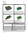
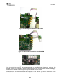
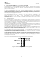
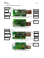
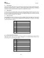
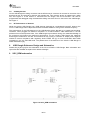
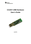
CC1111/CC2511 USB HW User’s Guide swru082b swru082b Table of Contents 1 2 3 4 5 6 Introduction......................................................................................................................................3 About this Manual............................................................................................................................3 Acronyms .........................................................................................................................................3 Definitions........................................................................................................................................4 Getting Started.................................................................................................................................5 Using SmartRF04EB as an In-Circuit Emulator (ICE).....................................................................7 6.1 The Debug Interface ...................................................................................................................7 7 USB Dongle Hardware Description .................................................................................................8 7.1 User Interface .............................................................................................................................9 7.2 USB Interface .............................................................................................................................9 7.3 Debug Connector........................................................................................................................9 7.4 General Purpose I/O Connectors ................................................................................................9 7.5 Cutaway Section.......................................................................................................................10 7.6 RF Performance of Antenna......................................................................................................10 8 USB Dongle Reference Design and Schematics ..........................................................................10 9 SOC_DEM schematics...................................................................................................................10 10 References..................................................................................................................................11 11 General Information ...................................................................................................................12 11.1 Document History..................................................................................................................12 2/12 swru082b 1 Introduction Thank you for purchasing a development kit for Low Power RF System-on-Chips from Texas Instruments. 2 About this Manual This manual covers the CC1111 USB Dongle or the CC2511 USB Dongle found in the CC1110CC1111DK/CC2510-CC2511DK development kits. Both these USB dongles are also available separately as the CC1111EMK868-915 and CC2511EMK evaluation module kits. The manual covers the CC1111/CC2511 USB Dongle hardware component of a USB development framework. Please refer to [5] and [6] for a description of the accompanying software library and application examples. 3 Acronyms CDC DK EB EM HID IC ICE KB LED LPRF MCU NC RF RX SoC TI TX UART USB Communications Device Class Development Kit Evaluation Board Evaluation Module Human Interface Device Integrated Circuit In Circuit Emulator Kilo Byte (1024 byte) Light Emitting Diode Low Power RF Micro Controller Not connected Radio Frequency Receive System on Chip Texas Instruments Transmit Universal Asynchronous Receive Transmit Universal Serial Bus 3/12 swru082b 4 Definitions SmartRF04EB CC1110EM/CC2510EM Evaluation Board. Main board in the development kits, USB interface, LCD, LEDs, pot-meter etc. Development platform for the Evaluation Modules (EM). CC1110 and CC2510 Evaluation Module are small modules for the CC1110 and CC2510 devices. These can be plugged into the SmartRF04EB and they should be used as the reference design for antenna and RF layout. CC1111/CC2511 USB Dongle System-on-Chip Debug Plug-in Board A reference design for a CC1111/CC2511 based full-speed USB dongle with RF interface. Should be used as reference design for antenna and RF layout. The System-on-Chip Debug Plug-In Board. It provides an additional physical debug/programming interface for the SmartRF04EB. Referred to as SOC_DEM in this document. Figure 1. Kit Hardware Component Overview SoC System on Chip. A collective term used to refer to Texas Instruments ICs with on-chip MCU and RF transceiver. Used in this document to reference the CC1111/CC2511 and the CC1110/CC2510. ICE In Circuit Emulator. ICE functionality is built into the SmartRF04EB. USB Software Application Examples Application examples using the CC1111/CC2511 USB Dongle together with a CC1110/CC2510EM. USB Firmware Library A library of low level USB firmware which is used by all the USB software examples. Table 1. Key Definitions See Figure 1 for an overview of the hardware components contained in the CC1110-CC1111DK/CC2510CC2511DK development kits. Table 1 explains some of the key definitions/abbreviations used in this document. 4/12 swru082b 5 Getting Started Make sure to install SmartRF Studio before connecting the SmartRF04EB to a PC. By installing it, the required Windows drivers will be provided when connecting the SmartRF04EB. SmartRF Studio [2] is a PC application for Windows that helps you find and adjust the radio register settings. Please see [2] for instructions on downloading and installing SmartRF Studio. The USB dongle is not delivered with pre-programmed firmware so an external ICE is needed for initial programming of the device. The SmartRF04EB or the CC-Debugger can be used to program the USB dongle. The CC1111/CC2511 has a 2 wire debug interface that is used for chip programming and debugging. When connecting this interface to the SmartRF04EB, the CC1111/CC2511 can be programmed from the SmartRF Flash Programmer software [4] and debugged from IAR Embedded Workbench. To connect the CC1111/CC2511 USB Dongle to the SmartRF04EB, follow these 7 steps: 1. Turn off the SmartRF04EB power by moving the power switch shown in Figure 4 to the left position. 2. Remove any evaluation modules (EMs) attached to the SmartRF04EB. 3. Connect the SmartRF04EB to a PC with the supplied USB cable. 4. Connect the System-on-Chip Debug Plug-In Board (SOC_DEM) to the EM connectors (P1 and P2) on the SmartRF04EB. 5. Connect the USB Dongle to the SOC_DEM with the supplied 10 pin cable. The cable should be mounted between the “Debug” connector on the dongle and the P3 connector on the SOC_DEM. Make sure pin 1 on the dongle is connected to pin 1 on the SOC_DEM (truncated corner). This cable connects the debug interface and GND between the two devices; however the USB Dongle is not powered through this cable. 6. Power the CC1111/CC2511 USB Dongle. To power the dongle there are two options: Powered with a USB Cable Use the supplied USB extension cable to connect the USB Dongle to the PC (see Figure 2). Powered from the SmartRF04EB Connect pin 9 on the “Test pin” connector on USB Dongle to pin 3 (labelled “3.3 V”) on the “I/O B” connector on SmartRF04EB to power the dongle from the EB (see Figure 3). The CC1111/CC2511 USB Dongle should only be powered by one of the two sources at a time. Do not connect the USB cable to the USB Dongle while it is powered from the SmartRF04EB. The SOC_DEM has a voltage level converter on the P3 connector, so the SmartRF04EB and the USB Dongle may have a different power supply voltage. 7. Turn on the power on the SmartRF04EB (see Figure 4). 5/12 swru082b Figure 2. USB Dongle Powered from USB Cable Figure 3. USB Dongle Powered from SmartRF04EB Figure 4. SmartRF04EB Power Switch, Power On The CC1111/CC2511 can now be programmed with the SmartRF Flash Programmer software. The firmware on the CC1111/CC2511 can also be debugged using the IAR Embedded Workbench debugger. Please see the SmartRF Flash Programmer [2] user manual for more details. Please see the “CC1110DK/CC2510DK Development Kit User Manual” [1] for more information on the SmartRF04EB and how to use the CC1110/CC2510EMs. 6/12 swru082b 6 Using SmartRF04EB as an In-Circuit Emulator (ICE) The debug interface on the SmartRF04EB is controlled by the USB MCU. This allows both programming and an emulator interface over USB, which makes the SmartRF04EB usable as an In-Circuit Emulator (ICE) for the CC1111/CC2511. To use the SmartRF04EB as ICE, the IAR Embedded Workbench software for 8051 architecture (EW8051) must be installed. The Embedded Workbench is an integrated development environment with a complete tool-chain such as C Compiler, Simulator, and ICE debugger. Please see [1] for instructions on how to set up the ICE debugger for use as an ICE. When the SmartRF04EB with a SoC is connected to a PC with the USB port, the debugger in IAR EW8051 will connect to it when started. If several SmartRF04EBs are connected to USB ports simultaneously, a selection window will display the connected evaluation boards, and the user can select which device to load. 6.1 The Debug Interface For custom PCB’s with e.g. the CC2511 SoC, it is recommended to include a pin header or test points to allow in-circuit emulation or programming using a SmartRF04EB or other 3rd party programming tools. The USB Dongle can be used as a reference. Please see the CC1110/CC2510/CC1111/CC2511 section of the TI web site for an updated list of 3rd party programming tools. VDD note: The SmartRF04EB includes a voltage converter to support programming and debugging of external systems with different voltage than the SmartRF04EB. The debug connector includes two VDD connections on pin 2 and pin 9. The function is different for these connections. Pin 2 VDD supplies voltage from the external target to the voltage converter. If the target application is self powered pin 2 should be connected to VDD to assure that the correct supply voltage is used for the voltage converter. This pin must always be connected to VDD. Pin 9 VDD supplies VDD (3.3 V) from the SmartRF04EB. If the target application is powered from the SmartRF04EB supply during programming and debugging this pin can be connected to VDD. If the target voltage differs from 3.3V, this pin should not be connected. On the USB Dongle this pin is not connected. Hence the USB Dongle must be powered from either a separate USB cable or a separate cable connecting pin 9 on P4 / “test pins” on the dongle to VDD on the SmartRF04EB. When using SmartRF04EB as emulator for external target debugging any evaluation module (EM) must be removed. Figure 5 shows the required signal for a minimum connector layout on external target. Figure 5. Minimum Debug Connector Pinout (top view) 7/12 swru082b 7 USB Dongle Hardware Description CC2511F32 LED PCB antenna Button Line marking cutaway section of the dongle USB connector Debug connector GPIO test pins Figure 6. CC2511 USB Dongle, (top view) Alternative debug connector Figure 7. CC2511 USB Dongle, (back view) CC1111F32 Chip antenna with PCB track LED USB connector Line marking cutaway section of the dongle Button Debug connector Figure 8. CC1111 USB Dongle, (top view) GPIO test pins Alternative debug connector Figure 9. CC1111 USB Dongle, (back view) 8/12 swru082b 7.1 User Interface The CC1111/CC2511 USB Dongle has one button and one LED that can be used to interact with the user. The LED is connected to pin P1_1. Setting P1_1 high (to logic 1) will turn the LED on. The button is connected to pin P1_2 and GND. The pin P1_2 must be configured as an input with pull-up for the button to operate as intended. When the button is pushed, P1_2 is pulled low (to logic 0). 7.2 USB Interface The USB Dongle has a standard USB connector. The dongle is powered through this connector. On the D+ line there is a pull-up used to identify the dongle as a full-speed USB device on the USB bus. The pullup can be controlled from the firmware, using P1_0. This enables the dongle to be connected to the USB bus without signalling its presence to the USB hub. 7.3 Debug Connector The USB Dongle has debug connector (P3) that is compatible with the SoC debug connector on the SmartRF04EB (P14) and on the System-on-Chip Debug Plug-In board (SOC_DEM) (P3). This enables the USB Dongle to be programmed and debugged via the SmartRF04EB. The pin-out of the debug connector (P3) is given in Table 2. Pin Function 1 GND 2 VDD 3 P2_2 / debug clock 4 P2_1 / debug data 5 P1_4 6 P1_5 7 RESET_N 8 P1_6 9 Not connected (VDD by mounting R6, 0 Ohm) 10 P1_7 Table 2. Debug Connector (P3) Pin-Out 7.4 General Purpose I/O Connectors All GPIO pins on the CC1111/CC2511 SoC that are not used on the USB Dongle are routed to the P4 “Test pins” pin-row. They can be used for debugging or to connect external devices to the CC1111/CC2511. The pin-out is given in Table 3. Pin Function 1 P2_0 2 GND 3 P0_5 4 P0_4 5 P0_3 6 P0_2 7 P0_1 8 P0_0 9 VDD 10 P1_3 Table 3. Test Pins (P4) Pin-Out 9/12 swru082b 7.5 Cutaway Section On the USB Dongle the debug connector and the GPIO test-pin connector is mounted on a section of the dongle that may be removed to minimize the dongles size. This cutaway section is marked with a white line, see Figure 8. If this section is removed from the dongle, the CC1111/CC2511 can still be programmed and debugged using the alternative debug connector found on the back of the USB Dongle, see Figure 7. 7.6 RF Performance of Antenna While the CC2511 USB Dongle has a PCB antenna designed as a meandered inverted F antenna, the CC1111 USB Dongle has a chip antenna with a PCB track added for tuning of the resonant frequency. The performance of the PCB antenna on the USB Dongle will be affected by its nearby surroundings. Therefore, when plugged into different computers or a USB extension cable differences in the RF performance must be expected. Also, if the USB Dongle is put inside a casing, the material and design of the enclosure will influence the antenna’s performance. For the CC2511 USB Dongle the maximum antenna gain measured is 5.3 dBi. This means that duty cycling or reduction of output power might be needed to ensure compliance with regulatory limits. Please see [7] for more information about SRD regulations in the 2.4 GHz ISM band. The performance of the antenna of the CC2511 USB Dongle is further described in [8]. 8 USB Dongle Reference Design and Schematics Please see [9] and [10] for the schematics of the CC1111/CC2511 USB Dongle. Both schematics and layout files are available as a part of the reference designs. 9 SOC_DEM schematics Figure 10. SOC_DEM schematics 10/12 swru082b 10 References [1] CC1110-CC1111DK CC2510-CC2511DK Development Kit User Manual (swru134) [2] SmartRF Flash Programmer (swrc044) [3] SmartRF Packet Sniffer (swrc045) [4] SmartRF Studio (swruc46) [5] CC USB Firmware Library and Examples (swrc088) [6] CC USB Software Examples User’s Guide (swru222) [7] AN032 – SRD Regulation for License-Free Transceiver Operation in the 2.4 GHz Band (swra060) [8] AN043 – Small Size 2.4 GHz PCB Antenna (swra117) [9] CC1111 USB Dongle Reference Design (swrr049) [10] CC2511 USB-Dongle Reference Design (swrc062) 11/12 swru082b 11 General Information 11.1 Document History Revision SWRU082B SWRU082A SWRU082 Date 2009.07.31 2009.05.08 2006.07.06 Description/Changes Updated hardware pictures and corrected a few typos Renamed. Moved software sections to swru222.pdf Initial release 12/12 IMPORTANT NOTICE Texas Instruments Incorporated and its subsidiaries (TI) reserve the right to make corrections, modifications, enhancements, improvements, and other changes to its products and services at any time and to discontinue any product or service without notice. Customers should obtain the latest relevant information before placing orders and should verify that such information is current and complete. All products are sold subject to TI’s terms and conditions of sale supplied at the time of order acknowledgment. TI warrants performance of its hardware products to the specifications applicable at the time of sale in accordance with TI’s standard warranty. Testing and other quality control techniques are used to the extent TI deems necessary to support this warranty. Except where mandated by government requirements, testing of all parameters of each product is not necessarily performed. TI assumes no liability for applications assistance or customer product design. Customers are responsible for their products and applications using TI components. To minimize the risks associated with customer products and applications, customers should provide adequate design and operating safeguards. TI does not warrant or represent that any license, either express or implied, is granted under any TI patent right, copyright, mask work right, or other TI intellectual property right relating to any combination, machine, or process in which TI products or services are used. Information published by TI regarding third-party products or services does not constitute a license from TI to use such products or services or a warranty or endorsement thereof. Use of such information may require a license from a third party under the patents or other intellectual property of the third party, or a license from TI under the patents or other intellectual property of TI. Reproduction of TI information in TI data books or data sheets is permissible only if reproduction is without alteration and is accompanied by all associated warranties, conditions, limitations, and notices. Reproduction of this information with alteration is an unfair and deceptive business practice. TI is not responsible or liable for such altered documentation. Information of third parties may be subject to additional restrictions. Resale of TI products or services with statements different from or beyond the parameters stated by TI for that product or service voids all express and any implied warranties for the associated TI product or service and is an unfair and deceptive business practice. TI is not responsible or liable for any such statements. TI products are not authorized for use in safety-critical applications (such as life support) where a failure of the TI product would reasonably be expected to cause severe personal injury or death, unless officers of the parties have executed an agreement specifically governing such use. Buyers represent that they have all necessary expertise in the safety and regulatory ramifications of their applications, and acknowledge and agree that they are solely responsible for all legal, regulatory and safety-related requirements concerning their products and any use of TI products in such safety-critical applications, notwithstanding any applications-related information or support that may be provided by TI. Further, Buyers must fully indemnify TI and its representatives against any damages arising out of the use of TI products in such safety-critical applications. TI products are neither designed nor intended for use in military/aerospace applications or environments unless the TI products are specifically designated by TI as military-grade or "enhanced plastic." Only products designated by TI as military-grade meet military specifications. Buyers acknowledge and agree that any such use of TI products which TI has not designated as military-grade is solely at the Buyer's risk, and that they are solely responsible for compliance with all legal and regulatory requirements in connection with such use. TI products are neither designed nor intended for use in automotive applications or environments unless the specific TI products are designated by TI as compliant with ISO/TS 16949 requirements. Buyers acknowledge and agree that, if they use any non-designated products in automotive applications, TI will not be responsible for any failure to meet such requirements. Following are URLs where you can obtain information on other Texas Instruments products and application solutions: Products Amplifiers Data Converters DLP® Products DSP Clocks and Timers Interface Logic Power Mgmt Microcontrollers RFID RF/IF and ZigBee® Solutions amplifier.ti.com dataconverter.ti.com www.dlp.com dsp.ti.com www.ti.com/clocks interface.ti.com logic.ti.com power.ti.com microcontroller.ti.com www.ti-rfid.com www.ti.com/lprf Applications Audio Automotive Broadband Digital Control Medical Military Optical Networking Security Telephony Video & Imaging Wireless www.ti.com/audio www.ti.com/automotive www.ti.com/broadband www.ti.com/digitalcontrol www.ti.com/medical www.ti.com/military www.ti.com/opticalnetwork www.ti.com/security www.ti.com/telephony www.ti.com/video www.ti.com/wireless Mailing Address: Texas Instruments, Post Office Box 655303, Dallas, Texas 75265 Copyright © 2009, Texas Instruments Incorporated