1
CubeSuite+ Simulator for 78K0R/Kx3 V3.00.03
Release Note
R20UT2511EJ0100
Rev.1.00
February 25, 2013
Contents
Chapter 1. Target Devices ........................................................................................................................ 2
Chapter 2. User's Manuals ........................................................................................................................ 3
Chapter 3. Key Word for Uninstallation ..................................................................................................... 4
Chapter 4. Changes .................................................................................................................................. 5
4.1 Specifications changed ..................................................................................................................... 5
4.1.1 Simulation on CubeSuite+ V2.00.00............................................................................................... 5
Chapter 5. Cautions................................................................................................................................... 6
5.1 Differences between target devices and simulator ........................................................................... 6
5.1.1 Flash self programming function..................................................................................................... 6
5.1.2 Reset............................................................................................................................................... 7
5.1.3 Oscillation stabilization time of Clock Generator ............................................................................ 8
5.1.4 SFR with clock generator (AMPH/FSEL/HIOTRM) ........................................................................ 9
5.1.5 Noise reduction circuit for external-interrupt pin ........................................................................... 10
5.1.6 IIC bus simulation ......................................................................................................................... 10
5.1.7 External bus interface functions.................................................................................................... 11
5.1.8 DMA controller .............................................................................................................................. 12
5.1.9 Operation clock of timer array unit................................................................................................ 12
5.1.10 Input pulse interval measurement mode of timer array unit ....................................................... 12
5.1.11 Noise filter of timer array unit...................................................................................................... 12
5.1.12 Operation clock of serial array unit ............................................................................................. 12
5.1.13 Noise filter of serial array unit ..................................................................................................... 13
5.1.14 SFR 0/1 constant bit ................................................................................................................... 13
5.1.15 Comparator stabilization time of A/D converter .......................................................................... 13
5.1.16 Default voltage of AVREF0 pin and AVREF1 pin ............................................................................. 13
5.1.17 Interrupt response time ............................................................................................................... 14
5.1.18 Execution of illegal instructions................................................................................................... 14
5.2 Cautions for using simulator GUI .................................................................................................... 15
5.2.1 Cautions for controlling each windows ......................................................................................... 15
5.2.2 Cautions for closing simulator GUI window .................................................................................. 15
5.2.3 Cautions for showing help for the simulator GUI window ............................................................. 15
5.2.4 Cautions for disconnecting the debug tool ................................................................................... 15
5.2.5 Cautions for setting the Host Machine's language and region ..................................................... 16
R20UT2511EJ0100 Rev.1.00
February 25, 2013
Page 1 of 16
CubeSuite+ Simulator for 78K0R/Kx3 V3.00.03
Release Note
Chapter 1. Target Devices
Below is a list of devices supported by the 78K0R/Kx3 simulator.
Nickname
78K0R/KE3
78K0R/KF3
Device name
μPD78F1142, μPD78F1143, μPD78F1144, μPD78F1145, μPD78F1146,
μPD78F1142A, μPD78F1143A, μPD78F1144A, μPD78F1145A, μPD78F1146A
μPD78F1152, μPD78F1153, μPD78F1154, μPD78F1155, μPD78F1156,
μPD78F1152A, μPD78F1153A, μPD78F1154A, μPD78F1155A, μPD78F1156A
μPD78F1162, μPD78F1163, μPD78F1164, μPD78F1165, μPD78F1166,
78K0R/KG3
μPD78F1167, μPD78F1168,
μPD78F1162A, μPD78F1163A, μPD78F1164A, μPD78F1165A, μPD78F1166A,
μPD78F1167A, μPD78F1168A
78K0R/KH3
78K0R/KJ3
μPD78F1174, μPD78F1175, μPD78F1176, μPD78F1177, μPD78F1178,
μPD78F1174A, μPD78F1175A, μPD78F1176A, μPD78F1177A, μPD78F1178A
μPD78F1184A, μPD78F1185A, μPD78F1186A, μPD78F1187A, μPD78F1188A
R20UT2511EJ0100 Rev.1.00
February 25, 2013
Page 2 of 16
CubeSuite+ Simulator for 78K0R/Kx3 V3.00.03
Release Note
Chapter 2. User's Manuals
Please read the following user’s manuals together with this document.
Manual Name
Document Number
CubeSuite+ V1.01.00 78K0R Debug
R20UT0732EJ0100
CubeSuite+ V2.00.00 Message
R20UT2448EJ0100
R20UT2511EJ0100 Rev.1.00
February 25, 2013
Page 3 of 16
CubeSuite+ Simulator for 78K0R/Kx3 V3.00.03
Release Note
Chapter 3. Key Word for Uninstallation
To uninstall this product, use the integrated uninstaller (uninstalls CubeSuite+).
R20UT2511EJ0100 Rev.1.00
February 25, 2013
Page 4 of 16
CubeSuite+ Simulator for 78K0R/Kx3 V3.00.03
Release Note
Chapter 4. Changes
This chapter describes changes from V3.00.02 to V3.00.03.
4.1
Specifications changed
4.1.1
Simulation on CubeSuite+ V2.00.00
Support simulation on CubeSuite+ V2.00.00. There is no functional change.
R20UT2511EJ0100 Rev.1.00
February 25, 2013
Page 5 of 16
CubeSuite+ Simulator for 78K0R/Kx3 V3.00.03
Release Note
Chapter 5. Cautions
This section describes cautions for using 78K0R/Kx3 simulator. The following two types of caution are described:
•Differences between target devices and simulator : Differences from behavior of target devices due to simulator
specifications
•Cautions for using simulator GUI
5.1
: Cautions for using the simulator GUI window
Differences between target devices and simulator
5.1.1
Flash self programming function
The following differences exist between the target device and simulator regarding the flash self programming
function.
1. Operation when a pull-down resistor is connected to the FLMD0 pin
In the target device, whether the flash self programming mode can be set via software is determined
based on its resistance when a pull-down resistor is externally connected to the FLMD0 pin.
FLMD0 Pin Handling
Setting via Software
Pulled down with a resistance of 100k ohm or more
Available
Pulled down with a resistance of less than 100k ohm
Not guaranteed
On the other hand, in the simulator, connection of a pull-down resistor to the FLMD0 pin can be specified
in the I/O Panel window but this panel does not have the function to set the resistance value. As a result,
if connection of a pull-down resistor to the FLMD0 pin is specified, it is regarded as an operation
equivalent to that being pulled down with a resistance of 100k ohm or more.
R20UT2511EJ0100 Rev.1.00
February 25, 2013
Page 6 of 16
CubeSuite+ Simulator for 78K0R/Kx3 V3.00.03
Release Note
2. Errors that are not generated
The simulator does not generate the following errors.
Error
Function Name
Error Name
Return
value
Initialize function
Processing abortion due to interrupt occurrence
0x1F
Block blank check function
Processing abortion due to interrupt occurrence
0x1F
Block erase function
Erase error
0x1A
Processing abortion due to interrupt occurrence
0x1F
Write error
0x1C
Processing abortion due to interrupt occurrence
0x1F
Verify (internal verify) error
0x1B
Processing abortion due to interrupt occurrence
0x1F
Erase error
0x1A
Verify (internal verify) error
0x1B
Write error
0x1C
Processing abortion due to interrupt occurrence
0x1F
Write error
0x1C
Verify (internal verify) error
0x1D
Processing abortion due to interrupt occurrence
0x1F
Word write function
Block verify function
Set information function
EEPROM write function
5.1.2
Reset
If a reset is generated by the Power-on-Clear circuit (POC) or low-voltage detector (LVI) circuit, the simulator
will display "STANDBY" in the status bar. (The status is actually reset, not standby.)
And the behavior differs as follows if a reset is generated by the RESET pin.
[Target device]
Goes into reset status when the RESET pin goes to low level. Reset status is released when it goes to
high level.
[Simulator]
Does not go into reset status when the RESET pin goes to low level. When it goes to high level, the
simulator momentarily goes into reset status, and then the reset status is released immediately.
R20UT2511EJ0100 Rev.1.00
February 25, 2013
Page 7 of 16
CubeSuite+ Simulator for 78K0R/Kx3 V3.00.03
5.1.3
Release Note
Oscillation stabilization time of Clock Generator
The simulator does not simulate the clock oscillator oscillation stabilization time.
The oscillation stabilization time is always 0 seconds when a reset or standby is released, regardless of the
OSTS register settings. The OSTS register is set to the following values.
Initial value after reset, during STOP mode, when MSTOP of CSC register = 1: 0x00
MSTOP of CSC register = 0 after STOP mode release: Values shown in the following table
(Maximum value in the target device)
OSTS Setting Value
OSTC Value
8
0x80
9
0xc0
10
0xe0
11
0x3 (2 /fx)
0xf0
0x4 (213/fx)
0xf8
0x0 (2 /fx)
0x1 (2 /fx)
0x2 (2 /fx)
15
0xfc
17
0x6 (2 /fx)
0xfe
0x7 (218/fx)
0xff
0x5 (2 /fx)
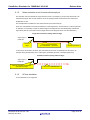
The following figure illustrates this operation.
In the target device, the X1 clock oscillation starts after the states (1) to (4) have passed. In the simulator,
states (1) to (4) end instantly and the X1 clock oscillation starts.
[In target device (an example of when OSTS is set to 0x07)]
X1 clock
oscillation
waveform
(1) STOP mode release or
MSTOP bit = 0
(OSTC register = 0x00)
(2) Time until oscillation
starts (OSTC register
= 0x00)
(3) Oscillation
stabilization time
(counted up in
OSTC register)
(4) OSTC register = 0xff
[In simulator (an example of when OSTS is set to 0x07)]
X1 clock
oscillation
waveform
STOP mode release or MSTOP bit = 0
(The OSTC register is set to 0xff at this moment.)
R20UT2511EJ0100 Rev.1.00
February 25, 2013
Page 8 of 16
CubeSuite+ Simulator for 78K0R/Kx3 V3.00.03
Release Note
Therefore, pay attention to the code that waits for oscillation stabilization.
There is no problem if a program is created with the condition that the execution exits the oscillation
stabilization wait period when the OSTC register value becomes the maximum value, or when the OSTC
register value exceeds the specified value, but if a program is created with the condition that the execution
exits the oscillation stabilization wait period when the OSTC register value becomes a value other than the
maximum value, the execution enters an infinite loop.
The following shows examples of code that causes/does not cause problems.
(This is an example of when OSTS is set to 0x07)
Correct program example (1)
Correct program example (2)
Example of program that may cause problems
while(OSTC != 0xff)
while(OSTC <= 0xf0)
while(OSTC != 0xf0)
{
{
{
NOP();/* wait */
NOP();/* wait */
NOP();/* wait */
}
}
}
5.1.4
SFR with clock generator (AMPH/FSEL/HIOTRM)
The simulator does not simulate the following SFRs, which belong to the clock generator. Read/write for
each register can be performed normally, but the operation does not change even if its value is changed.
Bit 0 (AMPH) of clock operation mode control register (CMC)
Bit 0 (FSEL) of operation speed mode control register (OSMC)
High-speed internal oscillator trimming register (HIOTRM)
[Bit 0 (AMPH) of clock operation mode control register (CMC)]
This register is used to set the oscillator gain according to the frequency when oscillating the high-speed
system clock. If a wrong setting is made, the high-speed system clock may not oscillate in the target
device. In the simulator, however, wrong settings do not affect the oscillation of the high-speed system
clock.
[Bit 0 (FSEL) of operation speed mode control register (OSMC)]
This register is used to control the step-up circuit for the high-speed flash memory operation.
If a wrong setting is made, read or instruction fetch from the flash memory may fail, or self programming
may fail in the target device. In the simulator, however, wrong settings do not affect the operation.
[High-speed internal oscillator trimming register (HIOTRM)]
This register is used to correct the high-speed internal oscillator accuracy. This register is provided in the
target device because the high-speed internal oscillator usually causes errors. In the simulator, however,
the high-speed internal oscillator does not cause errors, so it is not simulated.
R20UT2511EJ0100 Rev.1.00
February 25, 2013
Page 9 of 16
CubeSuite+ Simulator for 78K0R/Kx3 V3.00.03
5.1.5
Release Note
Noise reduction circuit for external-interrupt pin
The simulator does not simulate the noise reduction circuit. For example, if you input the active level to an
external-interrupt pin with a noise reduction circuit, the interrupt will be received even if the active-level
amplitude is too low.
The example below considers the case when there is input to the INTP0 pin.
There is a noise reduction circuit on the INTP0 pin of the target device. For this reason, in order to generate
an interrupt, it is necessary to input an effective edge to the target device, and subsequently maintain the
signal level. (See the user's manual of the target device for the length of time it must be maintained.)
Target device behavior (falling effective edge)
Signal input to
INTP0 pin
Effective
edge
Level must be maintained
(For 78K0R/KE3: 1 microsec)
Interrupt generated
In the case of the simulator, however, this noise reduction circuit is not simulated. For this reason, an
interrupt will be generated any time a valid edge is generated. (No need to maintain signal level).
Simulator behavior (falling effective edge)
Signal input to
INTP0 pin
Interrupt generated immediately
upon effective edge
5.1.6
No need to maintain level
IIC bus simulation
IIC bus simulation is not supported.
R20UT2511EJ0100 Rev.1.00
February 25, 2013
Page 10 of 16
CubeSuite+ Simulator for 78K0R/Kx3 V3.00.03
5.1.7
Release Note
External bus interface functions
Some of the external bus interface functions can be simulated, and some cannot.
[Functions that can be simulated]
* ROM and RAM connection
* Access to connected ROM/RAM
[Functions that cannot be simulated]
* External bus-related SFR simulation
(External bus access is possible even without configuring SFR.)
* Access speed simulation
(Access time is always 0 clock cycles. Additionally, signal input to the WAIT pin is ignored.)
* Check signal input to external bus pins in the [Timing Chart] window
(It will appear as high impedance.)
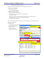
When connecting ROM or RAM to the external bus, perform configuration in the Property panel, from the
Debugging Tool Setting tab.
Connect by entering:
* Type of memory to connect to (emulation ROM area or emulation RAM area)
* Memory address to connect to
(2) Click this button
This setting enables both:
* Writing to external bus
* Reading from external bus
(1) Select this tab
(3) Set the type of external memory and address
(4) Click this button
R20UT2511EJ0100 Rev.1.00
February 25, 2013
Page 11 of 16
CubeSuite+ Simulator for 78K0R/Kx3 V3.00.03
5.1.8
Release Note
DMA controller
The transfer speeds of the target device and simulator differ as follows when simulating the DMA controller.
[Target device]
* It takes two clock cycles to complete one DMA transfer. The CPU waits during this period.
* If there is contention for transfer timing with another channel's DMA, then one of the DMA transfers will
be placed on hold; after the other DMA transfer is completed, the one on hold will begin.
[Simulator]
* It takes zero clock cycles to complete one DMA transfer. For this reason, the CPU does not wait.
* If there is contention for transfer timing with another channel's DMA, then both of the DMA transfers are
performed simultaneously.
5.1.9
Operation clock of timer array unit
Do not specify an operation clock that is 233 Hz or lower. If the operation clock (CKmk) of the timer array
unit (m=0 or 1, k=0 or 1) is 233 Hz or lower, then the timer array unit will not operate correctly (it will behave
as if operating via a clock that is faster than the one selected).
5.1.10
Input pulse interval measurement mode of timer array unit
When the input pulse interval measurement mode of the timer array unit is being used, the behavior when
an effective edge is detected on the Tlmn (mn = 00-07 or 10-13) pin differs.
[Target device]
The TCRmn timer counter register (mn=00-07 or 10-13) is initialized to 0x0000.
[Simulator]
The TCRmn timer counter register (mn=00-07 or 10-13) is to 0xFFFF.
For this reason, the pulse width count will be one less than on the target device.
5.1.11
Noise filter of timer array unit
Although the target device's timer array unit has a function to turn the noise filter on and off in order to
reduce noise on the timer input pin, the simulator does not simulate this. (There is no difference in behavior
whether filtering is on or off.) Since there is no noise in the simulator's signal, it would be meaningless to
simulate this function.
5.1.12
Operation clock of serial array unit
Do not use INTTM02 or INTTM03 as the operation clock for the serial array unit. (Doing so will prevent the
serial array unit from operating at all.)
R20UT2511EJ0100 Rev.1.00
February 25, 2013
Page 12 of 16
CubeSuite+ Simulator for 78K0R/Kx3 V3.00.03
5.1.13
Release Note
Noise filter of serial array unit
Although the target device's serial array unit has a function to turn the noise filter on and off in order to
reduce noise on the input pin, the simulator does not simulate this. (There is no difference in behavior
whether filtering is on or off.) Since there is no noise in the simulator's signal, it would be meaningless to
simulate this function.
5.1.14
SFR 0/1 constant bit
The SFR has bits that are always 0 or 1.
For example, bits 3 to 7 are always 0 for the oscillation stabilization time selection register (OSTS).
OSTS
7
0
6
0
5
0
4
0
3
0
2
OSTS2
1
OSTS1
0
OSTS0
Bits are always 0
Although the values of these bits cannot be changed in the case of the target device, the values can be
changed in the case of the simulator. Note that changing these values has no effect on behavior.
5.1.15
Comparator stabilization time of A/D converter
The comparator stabilization times of the A/D converter are different for the target device and simulator.
[Target device]
It takes 1 microsecond from the start of operation of the comparator until it stabilizes. Any A/D conversion
results obtained before stabilization will be invalid. For this reason, it is necessary to ignore the first A/D
conversion results.
[Simulator]
Comparator operation stabilizes immediately upon startup. For this reason, A/D conversion results
obtained within 1 microsecond of the start of operation will be correct, and there is thus no need to ignore
the first A/D conversion results.
5.1.16
Default voltage of AVREF0 pin and AVREF1 pin
Default voltage of AVREF0 pin is 5.0V. And default voltage of AVREF1 pin is 3.6V.
Note : The meaning of "Default voltage " is the voltage when the pin have no connection.
R20UT2511EJ0100 Rev.1.00
February 25, 2013
Page 13 of 16
CubeSuite+ Simulator for 78K0R/Kx3 V3.00.03
5.1.17
Release Note
Interrupt response time
The interrupt response times of the target device and simulator differ.
[Target device]
It takes 9 to 14 clock cycles from the generation of an interrupt until actual vector interrupt processing
begins.
[Simulator]
Vector interrupt processing begins immediately upon the interrupt.
5.1.18
Execution of illegal instructions
If an illegal instruction (instruction code: 0xFF) is executed, the target device will be reset, but the simulator
will go into an infinite loop (the illegal instruction will be executed repeatedly).
R20UT2511EJ0100 Rev.1.00
February 25, 2013
Page 14 of 16
CubeSuite+ Simulator for 78K0R/Kx3 V3.00.03
5.2
Release Note
Cautions for using simulator GUI
5.2.1
Cautions for controlling each windows
The following keyboard operations are not available in the simulator windows (signal-data editor window, I/O
panel window, and serial window).
* Navigation via tab or arrow keys (←, ↑, →, ↓)
* Deletion via the Del or Backspace keys
* Copy & paste and other operations via the Ctrl + C, V, X, A, or Z keys.
Perform the above operations as follows.
* Navigation:
Navigate using the mouse.
* Deletion:
Right click and perform the action via the context menu.
* Copy & paste, etc.: Right click and perform the action via the context menu.
5.2.2
Cautions for closing simulator GUI window
The simulator GUI window can only be closed by disconnecting from the debugging tool, or by closing
CubeSuite+ proper. (The X button cannot be clicked.)
Additionally, although it appears that the X button can be pressed if Aero is enabled in Windows Vista,
pressing this button will not close the GUI window.
5.2.3
Cautions for showing help for the simulator GUI window
Pressing the F1 key in the simulator GUI window will not display the help if none of the internal windows are
visible (e.g. the I/O panel window).
To display the help for the simulator GUI window, from the GUI window's menu, select [Help] > [Main
Window].
5.2.4
Cautions for disconnecting the debug tool
CubeSuite+ may exit if the debugging tool is disconnected while any of the following dialog boxes is open
from the simulator GUI window. Make sure that the following dialog boxes are closed before disconnecting
the debugging tool.
•Save As
•Open
•New
•Color
•Font
•Customize
•Loop
•Select Pin
•Search Data
•Format (UART)
•Format (CSI)
•Message (e.g. Error)
R20UT2511EJ0100 Rev.1.00
February 25, 2013
•Parts Button Properties
•Analog Button Properties
•Parts Key Properties
•Parts Level Gauge Properties
•Parts Led Properties
•Parts Segment LED Properties
•Parts Matrix Led Properties
•Parts Buzzer Properties
•Pull up / Pull down
•Entry Bitmap
•Object Properties
Page 15 of 16
CubeSuite+ Simulator for 78K0R/Kx3 V3.00.03
5.2.5
Release Note
Cautions for setting the Host Machine's language and region
If a Japanese OS is installed on your Host Machine, then if the language or region is set to other than
Japanese/Japan, the menus and dialog-box names of the simulator GUI window will be shown in English.
Similarly, if a non-Japanese OS is installed on your Host Machine, then if the language or region is set to
Japanese/Japan, the menus and dialog-box names of the simulator GUI window will be shown in Japanese.
All trademarks and registered trademarks are the property of their respective owners.
R20UT2511EJ0100 Rev.1.00
February 25, 2013
Page 16 of 16
Notice
1.
Descriptions of circuits, software and other related information in this document are provided only to illustrate the operation of semiconductor products and application examples. You are fully responsible for
the incorporation of these circuits, software, and information in the design of your equipment. Renesas Electronics assumes no responsibility for any losses incurred by you or third parties arising from the
use of these circuits, software, or information.
2.
Renesas Electronics has used reasonable care in preparing the information included in this document, but Renesas Electronics does not warrant that such information is error free. Renesas Electronics
3.
Renesas Electronics does not assume any liability for infringement of patents, copyrights, or other intellectual property rights of third parties by or arising from the use of Renesas Electronics products or
assumes no liability whatsoever for any damages incurred by you resulting from errors in or omissions from the information included herein.
technical information described in this document. No license, express, implied or otherwise, is granted hereby under any patents, copyrights or other intellectual property rights of Renesas Electronics or
others.
4.
You should not alter, modify, copy, or otherwise misappropriate any Renesas Electronics product, whether in whole or in part. Renesas Electronics assumes no responsibility for any losses incurred by you or
5.
Renesas Electronics products are classified according to the following two quality grades: "Standard" and "High Quality". The recommended applications for each Renesas Electronics product depends on
third parties arising from such alteration, modification, copy or otherwise misappropriation of Renesas Electronics product.
the product's quality grade, as indicated below.
"Standard": Computers; office equipment; communications equipment; test and measurement equipment; audio and visual equipment; home electronic appliances; machine tools; personal electronic
equipment; and industrial robots etc.
"High Quality": Transportation equipment (automobiles, trains, ships, etc.); traffic control systems; anti-disaster systems; anti-crime systems; and safety equipment etc.
Renesas Electronics products are neither intended nor authorized for use in products or systems that may pose a direct threat to human life or bodily injury (artificial life support devices or systems, surgical
implantations etc.), or may cause serious property damages (nuclear reactor control systems, military equipment etc.). You must check the quality grade of each Renesas Electronics product before using it
in a particular application. You may not use any Renesas Electronics product for any application for which it is not intended. Renesas Electronics shall not be in any way liable for any damages or losses
incurred by you or third parties arising from the use of any Renesas Electronics product for which the product is not intended by Renesas Electronics.
6.
You should use the Renesas Electronics products described in this document within the range specified by Renesas Electronics, especially with respect to the maximum rating, operating supply voltage
range, movement power voltage range, heat radiation characteristics, installation and other product characteristics. Renesas Electronics shall have no liability for malfunctions or damages arising out of the
use of Renesas Electronics products beyond such specified ranges.
7.
Although Renesas Electronics endeavors to improve the quality and reliability of its products, semiconductor products have specific characteristics such as the occurrence of failure at a certain rate and
malfunctions under certain use conditions. Further, Renesas Electronics products are not subject to radiation resistance design. Please be sure to implement safety measures to guard them against the
possibility of physical injury, and injury or damage caused by fire in the event of the failure of a Renesas Electronics product, such as safety design for hardware and software including but not limited to
redundancy, fire control and malfunction prevention, appropriate treatment for aging degradation or any other appropriate measures. Because the evaluation of microcomputer software alone is very difficult,
please evaluate the safety of the final products or systems manufactured by you.
8.
Please contact a Renesas Electronics sales office for details as to environmental matters such as the environmental compatibility of each Renesas Electronics product. Please use Renesas Electronics
products in compliance with all applicable laws and regulations that regulate the inclusion or use of controlled substances, including without limitation, the EU RoHS Directive. Renesas Electronics assumes
no liability for damages or losses occurring as a result of your noncompliance with applicable laws and regulations.
9.
Renesas Electronics products and technology may not be used for or incorporated into any products or systems whose manufacture, use, or sale is prohibited under any applicable domestic or foreign laws or
regulations. You should not use Renesas Electronics products or technology described in this document for any purpose relating to military applications or use by the military, including but not limited to the
development of weapons of mass destruction. When exporting the Renesas Electronics products or technology described in this document, you should comply with the applicable export control laws and
regulations and follow the procedures required by such laws and regulations.
10. It is the responsibility of the buyer or distributor of Renesas Electronics products, who distributes, disposes of, or otherwise places the product with a third party, to notify such third party in advance of the
contents and conditions set forth in this document, Renesas Electronics assumes no responsibility for any losses incurred by you or third parties as a result of unauthorized use of Renesas Electronics
products.
11. This document may not be reproduced or duplicated in any form, in whole or in part, without prior written consent of Renesas Electronics.
12. Please contact a Renesas Electronics sales office if you have any questions regarding the information contained in this document or Renesas Electronics products, or if you have any other inquiries.
(Note 1)
"Renesas Electronics" as used in this document means Renesas Electronics Corporation and also includes its majority-owned subsidiaries.
(Note 2)
"Renesas Electronics product(s)" means any product developed or manufactured by or for Renesas Electronics.
SALES OFFICES
http://www.renesas.com
Refer to "http://www.renesas.com/" for the latest and detailed information.
Renesas Electronics America Inc.
2880 Scott Boulevard Santa Clara, CA 95050-2554, U.S.A.
Tel: +1-408-588-6000, Fax: +1-408-588-6130
Renesas Electronics Canada Limited
1101 Nicholson Road, Newmarket, Ontario L3Y 9C3, Canada
Tel: +1-905-898-5441, Fax: +1-905-898-3220
Renesas Electronics Europe Limited
Dukes Meadow, Millboard Road, Bourne End, Buckinghamshire, SL8 5FH, U.K
Tel: +44-1628-651-700, Fax: +44-1628-651-804
Renesas Electronics Europe GmbH
Arcadiastrasse 10, 40472 Düsseldorf, Germany
Tel: +49-211-65030, Fax: +49-211-6503-1327
Renesas Electronics (China) Co., Ltd.
7th Floor, Quantum Plaza, No.27 ZhiChunLu Haidian District, Beijing 100083, P.R.China
Tel: +86-10-8235-1155, Fax: +86-10-8235-7679
Renesas Electronics (Shanghai) Co., Ltd.
Unit 204, 205, AZIA Center, No.1233 Lujiazui Ring Rd., Pudong District, Shanghai 200120, China
Tel: +86-21-5877-1818, Fax: +86-21-6887-7858 / -7898
Renesas Electronics Hong Kong Limited
Unit 1601-1613, 16/F., Tower 2, Grand Century Place, 193 Prince Edward Road West, Mongkok, Kowloon, Hong Kong
Tel: +852-2886-9318, Fax: +852 2886-9022/9044
Renesas Electronics Taiwan Co., Ltd.
13F, No. 363, Fu Shing North Road, Taipei, Taiwan
Tel: +886-2-8175-9600, Fax: +886 2-8175-9670
Renesas Electronics Singapore Pte. Ltd.
80 Bendemeer Road, Unit #06-02 Hyflux Innovation Centre Singapore 339949
Tel: +65-6213-0200, Fax: +65-6213-0300
Renesas Electronics Malaysia Sdn.Bhd.
Unit 906, Block B, Menara Amcorp, Amcorp Trade Centre, No. 18, Jln Persiaran Barat, 46050 Petaling Jaya, Selangor Darul Ehsan, Malaysia
Tel: +60-3-7955-9390, Fax: +60-3-7955-9510
Renesas Electronics Korea Co., Ltd.
11F., Samik Lavied' or Bldg., 720-2 Yeoksam-Dong, Kangnam-Ku, Seoul 135-080, Korea
Tel: +82-2-558-3737, Fax: +82-2-558-5141
© 2013 Renesas
Electronics
CorporationCorporation.
and Renesas
Corp.
© 2013
Renesas Electronics
AllSolutions
rights reserved.
Colophon 2.2
Colophon 2.2