1
Application Note
78K0R/Kx3
16-bit Single-Chip Microcontrollers
Flash Memory Programming (Programmer)
μPD78F1142
μPD78F1143
μPD78F1144
μPD78F1145
μPD78F1146
μPD78F1152
μPD78F1153
μPD78F1154
μPD78F1155
μPD78F1156
Document No. U18433EJ2V0AN00 (2nd edition)
Date Published April 2007 N
2007
Printed in Japan
μPD78F1162
μPD78F1163
μPD78F1164
μPD78F1165
μPD78F1166
μPD78F1167
μPD78F1168
[MEMO]
2
Application Note U18433EJ2V0AN
NOTES FOR CMOS DEVICES
1
VOLTAGE APPLICATION WAVEFORM AT INPUT PIN
Waveform distortion due to input noise or a reflected wave may cause malfunction. If the input of the
CMOS device stays in the area between VIL (MAX) and VIH (MIN) due to noise, etc., the device may
malfunction. Take care to prevent chattering noise from entering the device when the input level is fixed,
and also in the transition period when the input level passes through the area between VIL (MAX) and
VIH (MIN).
2
HANDLING OF UNUSED INPUT PINS
Unconnected CMOS device inputs can be cause of malfunction. If an input pin is unconnected, it is
possible that an internal input level may be generated due to noise, etc., causing malfunction. CMOS
devices behave differently than Bipolar or NMOS devices. Input levels of CMOS devices must be fixed
high or low by using pull-up or pull-down circuitry. Each unused pin should be connected to VDD or GND
via a resistor if there is a possibility that it will be an output pin. All handling related to unused pins must
be judged separately for each device and according to related specifications governing the device.
3
PRECAUTION AGAINST ESD
A strong electric field, when exposed to a MOS device, can cause destruction of the gate oxide and
ultimately degrade the device operation. Steps must be taken to stop generation of static electricity as
much as possible, and quickly dissipate it when it has occurred.
Environmental control must be
adequate. When it is dry, a humidifier should be used. It is recommended to avoid using insulators that
easily build up static electricity. Semiconductor devices must be stored and transported in an anti-static
container, static shielding bag or conductive material. All test and measurement tools including work
benches and floors should be grounded.
The operator should be grounded using a wrist strap.
Semiconductor devices must not be touched with bare hands. Similar precautions need to be taken for
PW boards with mounted semiconductor devices.
4
STATUS BEFORE INITIALIZATION
Power-on does not necessarily define the initial status of a MOS device. Immediately after the power
source is turned ON, devices with reset functions have not yet been initialized. Hence, power-on does
not guarantee output pin levels, I/O settings or contents of registers. A device is not initialized until the
reset signal is received. A reset operation must be executed immediately after power-on for devices
with reset functions.
5
POWER ON/OFF SEQUENCE
In the case of a device that uses different power supplies for the internal operation and external
interface, as a rule, switch on the external power supply after switching on the internal power supply.
When switching the power supply off, as a rule, switch off the external power supply and then the
internal power supply. Use of the reverse power on/off sequences may result in the application of an
overvoltage to the internal elements of the device, causing malfunction and degradation of internal
elements due to the passage of an abnormal current.
The correct power on/off sequence must be judged separately for each device and according to related
specifications governing the device.
6
INPUT OF SIGNAL DURING POWER OFF STATE
Do not input signals or an I/O pull-up power supply while the device is not powered. The current
injection that results from input of such a signal or I/O pull-up power supply may cause malfunction and
the abnormal current that passes in the device at this time may cause degradation of internal elements.
Input of signals during the power off state must be judged separately for each device and according to
related specifications governing the device.
Application Note U18433EJ2V0AN
3
• The information in this document is current as of January, 2007. The information is subject to
change without notice. For actual design-in, refer to the latest publications of NEC Electronics data
sheets or data books, etc., for the most up-to-date specifications of NEC Electronics products. Not
all products and/or types are available in every country. Please check with an NEC Electronics sales
representative for availability and additional information.
• No part of this document may be copied or reproduced in any form or by any means without the prior
written consent of NEC Electronics. NEC Electronics assumes no responsibility for any errors that may
appear in this document.
• NEC Electronics does not assume any liability for infringement of patents, copyrights or other intellectual
property rights of third parties by or arising from the use of NEC Electronics products listed in this document
or any other liability arising from the use of such products. No license, express, implied or otherwise, is
granted under any patents, copyrights or other intellectual property rights of NEC Electronics or others.
• Descriptions of circuits, software and other related information in this document are provided for illustrative
purposes in semiconductor product operation and application examples. The incorporation of these
circuits, software and information in the design of a customer's equipment shall be done under the full
responsibility of the customer. NEC Electronics assumes no responsibility for any losses incurred by
customers or third parties arising from the use of these circuits, software and information.
• While NEC Electronics endeavors to enhance the quality, reliability and safety of NEC Electronics products,
customers agree and acknowledge that the possibility of defects thereof cannot be eliminated entirely. To
minimize risks of damage to property or injury (including death) to persons arising from defects in NEC
Electronics products, customers must incorporate sufficient safety measures in their design, such as
redundancy, fire-containment and anti-failure features.
• NEC Electronics products are classified into the following three quality grades: "Standard", "Special" and
"Specific".
The "Specific" quality grade applies only to NEC Electronics products developed based on a customerdesignated "quality assurance program" for a specific application. The recommended applications of an NEC
Electronics product depend on its quality grade, as indicated below. Customers must check the quality grade of
each NEC Electronics product before using it in a particular application.
"Standard": Computers, office equipment, communications equipment, test and measurement equipment, audio
and visual equipment, home electronic appliances, machine tools, personal electronic equipment
and industrial robots.
"Special": Transportation equipment (automobiles, trains, ships, etc.), traffic control systems, anti-disaster
systems, anti-crime systems, safety equipment and medical equipment (not specifically designed
for life support).
"Specific": Aircraft, aerospace equipment, submersible repeaters, nuclear reactor control systems, life
support systems and medical equipment for life support, etc.
The quality grade of NEC Electronics products is "Standard" unless otherwise expressly specified in NEC
Electronics data sheets or data books, etc. If customers wish to use NEC Electronics products in applications
not intended by NEC Electronics, they must contact an NEC Electronics sales representative in advance to
determine NEC Electronics' willingness to support a given application.
(Note)
(1) "NEC Electronics" as used in this statement means NEC Electronics Corporation and also includes its
majority-owned subsidiaries.
(2) "NEC Electronics products" means any product developed or manufactured by or for NEC Electronics (as
defined above).
M8E 02. 11-1
4
Application Note U18433EJ2V0AN
INTRODUCTION
Target Readers
This application note is intended for users who understand the functions of the
78K0R/Kx3 and who will use this product to design application systems.
Purpose
The purpose of this application note is to help users understand how to develop
dedicated flash memory programmers for rewriting the internal flash memory of the
78K0R/Kx3.
The sample programs and circuit diagrams shown in this document are for reference
only and are not intended for use in actual design-ins.
Therefore, these sample programs must be used at the user’s own risk.
Correct
operation is not guaranteed if these sample programs are used.
Organization
This manual consists of the following main sections.
• Flash memory programming
• Programmer operating environment
• Basic programmer operation
• Command/data frame format
• Description of command processing
• UART communication mode
• Flash memory programming parameter characteristics
How to Read This Manual
It is assumed that the reader of this manual has general knowledge in the fields of
electrical engineering, logic circuits, and microcontrollers.
• To gain a general understanding of functions:
→ Read this manual in the order of the CONTENTS.
• To learn more about the 78K0R/Kx3’s hardware functions:
→ See the user’s manual of each 78K0R/Kx3 product.
Conventions
Data significance:
Higher digits on the left and lower digits on the right
Active low representation:
xxx (overscore over pin or signal name)
Note:
Footnote for item marked with Note in the text
Caution:
Information requiring particular attention
Remark:
Supplementary information
Numeral representation:
Binary..................xxxx or xxxxB
Decimal ...............xxxx
Hexadecimal .......xxxxH
Application Note U18433EJ2V0AN
5
CONTENTS
CHAPTER 1 FLASH MEMORY PROGRAMMING ............................................................................... 10
1.1
1.2
1.3
1.4
Overview ..................................................................................................................................... 10
System Configuration................................................................................................................ 11
Programming Overview............................................................................................................. 12
1.3.1
Setting flash memory programming mode ......................................................................................12
1.3.2
Manipulating flash memory via command transmission/reception ..................................................13
Information Specific to 78K0R/Kx3 .......................................................................................... 14
CHAPTER 2 PROGRAMMER OPERATING ENVIRONMENT ............................................................. 16
2.1
2.2
2.3
2.4
2.5
2.6
2.7
2.8
2.9
Programmer Control Pins ......................................................................................................... 16
Details of Control Pins............................................................................................................... 17
2.2.1
Flash memory programming mode setting pin (FLMD0).................................................................17
2.2.2
Serial interface pin (TOOL0) ...........................................................................................................17
2.2.3
Reset control pin (RESET)..............................................................................................................18
2.2.4
VDD/GND control pins......................................................................................................................18
2.2.5
Other pins .......................................................................................................................................18
Basic Flowchart.......................................................................................................................... 19
Setting Flash Memory Programming Mode............................................................................. 20
2.4.1
Mode setting flowchart ....................................................................................................................21
2.4.2
Sample program .............................................................................................................................22
Single-Wire UART Communication Mode................................................................................ 23
Shutting Down Target Power Supply ....................................................................................... 23
Manipulation of Flash Memory ................................................................................................. 24
Command List ............................................................................................................................ 24
Status List ................................................................................................................................... 25
CHAPTER 3 BASIC PROGRAMMER OPERATION ............................................................................ 26
CHAPTER 4 COMMAND/DATA FRAME FORMAT ............................................................................. 27
4.1
4.2
4.3
Command Frame Transmission Processing........................................................................... 29
Data Frame Transmission Processing..................................................................................... 29
Data Frame Reception Processing........................................................................................... 29
CHAPTER 5 DESCRIPTION OF COMMAND PROCESSING ............................................................. 30
5.1
5.2
5.3
6
Status Command........................................................................................................................ 30
5.1.1
Description......................................................................................................................................30
5.1.2
Status frame ...................................................................................................................................30
Reset Command ......................................................................................................................... 31
5.2.1
Description......................................................................................................................................31
5.2.2
Command frame and status frame..................................................................................................31
Baud Rate Set Command .......................................................................................................... 32
5.3.1
Description......................................................................................................................................32
5.3.2
Command frame and status frame..................................................................................................32
Application Note U18433EJ2V0AN
5.4
5.5
5.6
5.7
5.8
5.9
Chip Erase Command.................................................................................................................34
5.4.1
Description...................................................................................................................................... 34
5.4.2
Command frame and status frame ................................................................................................. 34
Block Erase Command...............................................................................................................35
5.5.1
Description...................................................................................................................................... 35
5.5.2
Command frame and status frame ................................................................................................. 35
Programming Command ............................................................................................................36
5.6.1
Description...................................................................................................................................... 36
5.6.2
Command frame and status frame ................................................................................................. 36
5.6.3
Data frame and status frame .......................................................................................................... 36
5.6.4
Completion of transferring all data and status frame ...................................................................... 37
Verify Command .........................................................................................................................38
5.7.1
Description...................................................................................................................................... 38
5.7.2
Command frame and status frame ................................................................................................. 38
5.7.3
Data frame and status frame .......................................................................................................... 38
Block Blank Check Command...................................................................................................40
5.8.1
Description...................................................................................................................................... 40
5.8.2
Command frame and status frame ................................................................................................. 40
Silicon Signature Command ......................................................................................................41
5.9.1
Description...................................................................................................................................... 41
5.9.2
Command frame and status frame ................................................................................................. 41
5.9.3
Silicon signature data frame ........................................................................................................... 42
5.9.4
78K0R/Kx3 silicon signature list ..................................................................................................... 44
5.10 Version Get Command ...............................................................................................................49
5.10.1
Description...................................................................................................................................... 49
5.10.2
Command frame and status frame ................................................................................................. 49
5.10.3
Version data frame ......................................................................................................................... 50
5.11 Checksum Command .................................................................................................................51
5.11.1
Description...................................................................................................................................... 51
5.11.2
Command frame and status frame ................................................................................................. 51
5.11.3
Checksum data frame .................................................................................................................... 51
5.12 Security Set Command...............................................................................................................52
5.12.1
Description...................................................................................................................................... 52
5.12.2
Command frame and status frame ................................................................................................. 52
5.12.3
Data frame and status frame .......................................................................................................... 53
5.12.4
Internal verify check and status frame ............................................................................................ 53
CHAPTER 6
6.1
6.2
6.3
6.4
6.5
UART COMMUNICATION MODE ...................................................................................55
Command Frame Transmission Processing Flowchart .........................................................55
Data Frame Transmission Processing Flowchart ...................................................................56
Data Frame Reception Processing Flowchart .........................................................................57
Reset Command..........................................................................................................................58
6.4.1
Processing sequence chart ............................................................................................................ 58
6.4.2
Description of processing sequence ............................................................................................... 59
6.4.3
Status at processing completion..................................................................................................... 59
6.4.4
Flowchart ........................................................................................................................................ 60
6.4.5
Sample program ............................................................................................................................. 61
Baud Rate Set Command ...........................................................................................................62
Application Note U18433EJ2V0AN
7
6.6
6.7
6.8
6.9
6.5.1
Processing sequence chart.............................................................................................................62
6.5.2
Description of processing sequence ...............................................................................................63
6.5.3
Status at processing completion .....................................................................................................63
6.5.4
Flowchart ........................................................................................................................................64
6.5.5
Sample program .............................................................................................................................65
Chip Erase Command ................................................................................................................ 66
6.6.1
Processing sequence chart.............................................................................................................66
6.6.2
Description of processing sequence ...............................................................................................67
6.6.3
Status at processing completion .....................................................................................................67
6.6.4
Flowchart ........................................................................................................................................68
6.6.5
Sample program .............................................................................................................................69
Block Erase Command .............................................................................................................. 70
6.7.1
Processing sequence chart.............................................................................................................70
6.7.2
Description of processing sequence ...............................................................................................71
6.7.3
Status at processing completion .....................................................................................................71
6.7.4
Flowchart ........................................................................................................................................72
6.7.5
Sample program .............................................................................................................................73
Programming Command ........................................................................................................... 74
6.8.1
Processing sequence chart.............................................................................................................74
6.8.2
Description of processing sequence ...............................................................................................75
6.8.3
Status at processing completion .....................................................................................................76
6.8.4
Flowchart ........................................................................................................................................77
6.8.5
Sample program .............................................................................................................................78
Verify Command......................................................................................................................... 80
6.9.1
Processing sequence chart.............................................................................................................80
6.9.2
Description of processing sequence ...............................................................................................81
6.9.3
Status at processing completion .....................................................................................................81
6.9.4
Flowchart ........................................................................................................................................82
6.9.5
Sample program .............................................................................................................................83
6.10 Block Blank Check Command .................................................................................................. 85
6.10.1
Processing sequence chart.............................................................................................................85
6.10.2
Description of processing sequence ...............................................................................................86
6.10.3
Status at processing completion .....................................................................................................86
6.10.4
Flowchart ........................................................................................................................................87
6.10.5
Sample program .............................................................................................................................88
6.11 Silicon Signature Command ..................................................................................................... 89
6.11.1
Processing sequence chart.............................................................................................................89
6.11.2
Description of processing sequence ...............................................................................................90
6.11.3
Status at processing completion .....................................................................................................90
6.11.4
Flowchart ........................................................................................................................................91
6.11.5
Sample program .............................................................................................................................92
6.12 Version Get Command .............................................................................................................. 93
6.12.1
Processing sequence chart.............................................................................................................93
6.12.2
Description of processing sequence ...............................................................................................94
6.12.3
Status at processing completion .....................................................................................................94
6.12.4
Flowchart ........................................................................................................................................95
6.12.5
Sample program .............................................................................................................................96
6.13 Checksum Command ................................................................................................................ 97
8
Application Note U18433EJ2V0AN
6.13.1
Processing sequence chart ............................................................................................................ 97
6.13.2
Description of processing sequence ............................................................................................... 98
6.13.3
Status at processing completion..................................................................................................... 98
6.13.4
Flowchart ........................................................................................................................................ 99
6.13.5
Sample program ........................................................................................................................... 100
6.14 Security Set Command.............................................................................................................101
6.14.1
Processing sequence chart .......................................................................................................... 101
6.14.2
Description of processing sequence ............................................................................................. 102
6.14.3
Status at processing completion................................................................................................... 102
6.14.4
Flowchart ...................................................................................................................................... 103
6.14.5
Sample program ........................................................................................................................... 104
CHAPTER 7 FLASH MEMORY PROGRAMMING PARAMETER CHARACTERISTICS ................106
APPENDIX A CIRCUIT DIAGRAMS (REFERENCE) ..........................................................................122
Application Note U18433EJ2V0AN
9
CHAPTER 1 FLASH MEMORY PROGRAMMING
To rewrite the contents of the internal flash memory of the 78K0R/Kx3, a dedicated flash memory programmer
(hereafter referred to as the “programmer”) is usually used.
This application note explains how to develop a dedicated programmer.
1.1
Overview
The 78K0R/Kx3 incorporates firmware that controls flash memory programming. The programming to the internal
flash memory is performed by transmitting/receiving commands between the programmer and the 78K0R/Kx3 via
serial communication.
Figure 1-1. System Outline of Flash Memory Programming in 78K0R/Kx3
78K0R/Kx3
Firmware
Programmer
Serial
communication
CPU
Flash memory
10
Application Note U18433EJ2V0AN
CHAPTER 1 FLASH MEMORY PROGRAMMING
1.2
System Configuration
Examples of the system configuration for programming the flash memory are illustrated in Figure 1-2.
This figure illustrates how to program the flash memory with the programmer, under control of a host machine.
Depending on how the programmer is connected, the programmer can be used in a standalone mode without using
the host machine, if a user program has been downloaded to the programmer in advance.
For example, NEC Electronics’ flash memory programmer PG-FP4 can execute programming either by using the
GUI software with a host machine connected or by itself (standalone).
Figure 1-2. System Configuration
Single-wire UART communication mode (LSB-first transfer)
Host machine
Programmer
RS-232C/USB
Remark
78K0R/Kx3
VDD
VDD
VSS
VSS
RESET
RESET
TOOL0
TOOL0
FLMD0
FLMD0
Firmware
Flash
memory
The 78K0R/Kx3 can only communicate via the single-wire UART communication mode.
Application Note U18433EJ2V0AN
11
CHAPTER 1 FLASH MEMORY PROGRAMMING
1.3
Programming Overview
To rewrite the contents of the flash memory with the programmer, the 78K0R/Kx3 must first be set to the flash
memory programming mode. After that, transmit commands from the programmer via serial communication, and then
rewrite the flash memory. The flowchart of programming is illustrated in Figure 1-3.
Figure 1-3. Programming Flowchart
Start
Setting flash memory
programming mode
Manipulation of flash memory
via command transmission/
reception
No
Manipulation completed?
Yes
End
1.3.1
Setting flash memory programming mode
Supply a specific voltage to the flash memory programming mode setting pin (FLMD0) in the 78K0R/Kx3 and
release a reset; the flash memory programming mode is then set.
12
Application Note U18433EJ2V0AN
CHAPTER 1 FLASH MEMORY PROGRAMMING
1.3.2
Manipulating flash memory via command transmission/reception
The flash memory incorporated in the 78K0R/Kx3 has functions to rewrite the flash memory contents. The flash
memory manipulating functions shown in Table 1-1 are available.
Table 1-1. Outline of Flash Memory Functions
Function
Outline
Erase
Erases the flash memory contents.
Write
Writes data to the flash memory.
Verify
Compares the flash memory contents with data for verify.
Acquisition of information
Reads information related to the flash memory.
To control these functions, the programmer transmits commands to the 78K0R/Kx3 via serial communication. The
78K0R/Kx3 returns the response status for the commands. The programming to the flash memory is performed by
repeating these series of serial communications.
Application Note U18433EJ2V0AN
13
CHAPTER 1 FLASH MEMORY PROGRAMMING
1.4
Information Specific to 78K0R/Kx3
The programmer must manage product-specific information (such as a device name and memory information).
Table 1-2 shows the flash memory size of the 78K0R/Kx3 and Figure 1-4 shows the configuration of the flash
memory.
Table 1-2. Flash Memory Size of 78K0R/Kx3
Device Name
78K0R/KE3
78K0R/KF3
78K0R/KG3
14
μPD78F1142
Flash Memory Size
64 KB
μPD78F1143
96 KB
μPD78F1144
128 KB
μPD78F1145
192 KB
μPD78F1146
256 KB
μPD78F1152
64 KB
μPD78F1153
96 KB
μPD78F1154
128 KB
μPD78F1155
192 KB
μPD78F1156
256 KB
μPD78F1162
64 KB
μPD78F1163
96 KB
μPD78F1164
128 KB
μPD78F1165
192 KB
μPD78F1166
256 KB
μPD78F1167
384 KB
μPD78F1168
512 KB
Application Note U18433EJ2V0AN
CHAPTER 1 FLASH MEMORY PROGRAMMING
Figure 1-4. Flash Memory Configuration
<Block number>
2 KB
Block FFH
<Address>
<Flash memory size>
7FFFFH
512 KB
2 KB
Block C0H
2 KB
Block BFH
60000H
5FFFFH
384 KB
2 KB
Block 80H
2 KB
Block 7FH
40000H
3FFFFH
256 KB
2 KB
Block 60H
2 KB
Block 5FH
30000H
2FFFFH
192 KB
2 KB
Block 40H
2 KB
Block 3FH
20000H
1FFFFH
128 KB
2 KB
Block 30H
2 KB
Block 2FH
18000H
17FFFH
96 KB
2 KB
Block 20H
2 KB
Block 1FH
10000H
0FFFFH
64 KB
2 KB
Remark
Block 00H
00000H
Each block consists of 2 KB (this figure only illustrates some parts of entire blocks in the flash memory).
Application Note U18433EJ2V0AN
15
CHAPTER 2 PROGRAMMER OPERATING ENVIRONMENT
2.1
Programmer Control Pins
Table 2-1 lists the pins that the programmer must control to implement the programmer function in the user system.
See the following pages for details on each pin.
Table 2-1. Pin Description
Programmer
Signal Name
I/O
FLMD0
Output
VDD
I/O
78K0R/Kx3
Pin Function
Mode signal
Pin Name
Procedure When
Connecting
FLMD0
√
VDD
√
VDD voltage generation/monitoring
EVDD (0/1)
AVREF (0/1)Note
GND
−
Ground
VSS
√
EVSS (0/1)
AVSS
Clock output
−
Reset signal
RESET
√
Receive signal
TOOL0
√
−
×
CLK
Output
/RESET
Output
SI/RXD
Input
SO/TXD
Output
Transmit signal
SCK
Output
Transfer clock
×
Note When performing off-board write operation, connect this pin to VDD.
When performing on-board write operation, supply the same power as in normal operation mode. (At this
time, make sure to set so that VDD ≥ AVREF(0/1).)
Remark
√: Be sure to connect the pin.
×: The pin does not have to be connected.
For the voltage of the pins controlled by the programmer, refer to the user’s manual of the device that is subject to
flash memory programming.
16
Application Note U18433EJ2V0AN
CHAPTER 2 PROGRAMMER OPERATING ENVIRONMENT
2.2
2.2.1
Details of Control Pins
Flash memory programming mode setting pin (FLMD0)
The FLMD0 pin is used to control the operating mode of the 78K0R/Kx3. The 78K0R/Kx3 operates in flash
memory programming mode when a specific voltage is supplied to this pin and a reset is released.
2.2.2
Serial interface pin (TOOL0)
The serial interface pin is used to transfer the flash memory writing commands between the programmer and the
78K0R/Kx3.
The following figure illustrates the connection of pins used.
Figure 2-1. Serial Interface Pin
Programmer
78K0R/Kx3
TxD
RxD
TOOL0
Single-wire UART communication
Application Note U18433EJ2V0AN
17
CHAPTER 2 PROGRAMMER OPERATING ENVIRONMENT
2.2.3
Reset control pin (RESET)
The reset control pin (RESET pin) is used to control the system reset for the 78K0R/Kx3 from the programmer.
The flash memory programming mode can be selected when a specific voltage is supplied to the FLMD0 pin and a
reset is released.
Figure 2-2. RESET Pin
2.2.4
Programmer
78K0R/Kx3
Any port
RESET pin
VDD/GND control pins
The VDD control pin is used to supply power to the 78K0R/Kx3 from the programmer. Connection of this pin is not
necessary when it is not necessary to supply power to the 78K0R/Kx3 from the programmer. However, this pin must
be connected regardless of whether the power is supplied from the programmer when the dedicated programmer is
used, because the dedicated programmer monitors the power supply status of the 78K0R/Kx3.
The GND control pin must be connected to VSS of the 78K0R/Kx3 regardless of whether the power is supplied from
the programmer.
Figure 2-3. VDD/GND Control Pin
Programmer
VDD
78K0R/Kx3
VDD, EVDD (0/1),
AVREF (0/1)
Note
GND
VSS, EVSS (0/1), AVSS
Note When performing off-board write operation, connect this pin to VDD.
When performing on-board write operation, supply the same power as in normal
operation mode. (At this time, make sure to set so that VDD ≥ AVREF(0/1).)
2.2.5
Other pins
For the connection of the pins that are not connected to the programmer, refer to the chapter describing the flash
memory in the user’s manual of each device.
18
Application Note U18433EJ2V0AN
CHAPTER 2 PROGRAMMER OPERATING ENVIRONMENT
2.3
Basic Flowchart
The following illustrates the basic flowchart for performing flash memory rewriting with the programmer.
Figure 2-4. Basic Flowchart for Flash Memory Rewrite Processing
Basic flow
Power application to target
(See Figure 2-5)
Mode setting (reset release)
(See 2.4)
Synchronization processing
(Reset command)
(See 5.2)
Communication speed setting
(Baud Rate Set command)
(See 5.3)
Signature acquisition
(Silicon Signature command)
(See 5.9)
Command execution
Processing
completed?
No
Yes
Target power shutdown processing
(See 2.6)
Reset input and power shutdown during rewriting is
prohibited because security information may be
lost.
End
Application Note U18433EJ2V0AN
19
CHAPTER 2 PROGRAMMER OPERATING ENVIRONMENT
2.4
Setting Flash Memory Programming Mode
To rewrite the contents of the flash memory with the programmer, the 78K0R/Kx3 must first be set to the flash
memory programming mode by supplying a specific voltage to the flash memory programming mode setting pin
(FLMD0) in the 78K0R/Kx3, then releasing a reset.
The following illustrates a timing chart for setting the flash memory programming mode.
Figure 2-5. Setting Flash Memory Programming Mode
VDD
VDD
FLMD0
RESET
VDD
TOOL0
<1> <2>
<3>
<4>
<5>
<1>: Power application (VDD)
<2>: FLMD0 = high level
<3>: Reset release (serial programming mode setting)
<4>: READY pulse (“00”@9600 bps) input start (78K0R/Kx3 → programmer)
<5>: LOW pulse (“00”@9600 bps) output start (programmer → 78K0R/Kx3)
The relationship between the setting of the FLMD0 pin after reset release and the operating mode is shown below.
Table 2-2. Relationship Between FLMD0 Pin Setting After Reset Release and Operating Mode
FLMD0
20
Operating Mode
Low (GND)
Normal operating mode
High (VDD)
Flash memory programming mode
Application Note U18433EJ2V0AN
CHAPTER 2 PROGRAMMER OPERATING ENVIRONMENT
2.4.1
Mode setting flowchart
Transition processing to
programming mode
RESET pin low output
FLMD0 pin low output
VDD pin high output
(Target power supply on)
Wait
tDP (min.)
FLMD0 pin high output
Wait
tPR (min.)
RESET pin high output
NG
Ready pulse
check
OK
Start of time measurement
until start of reset command
processing
Abnormal termination
t01 (min.)
Initialization of UART
hardware
Has specified time
elapsed until start of
reset command
processing?
No
Yes
Normal termination
Application Note U18433EJ2V0AN
21
CHAPTER 2 PROGRAMMER OPERATING ENVIRONMENT
2.4.2
Sample program
The following shows a sample program for mode setting processing.
/****************************************************************/
/*
*/
/* connect to Flash device
*/
/*
*/
/****************************************************************/
u16
fl_con_dev(void)
{
extern void
init_fl_uart(void);
extern void
init_fl_csi(void);
extern void
stop_UART0(void);
u16
rc = NO_ERROR;
SRMK0 = true;
UARTE0 = false;
stop_UART0();
// disable UART Rx INT.
// disable UART H.W.
// TxD/RxD = Hi-Z
pFL_RES
= low;
pmFL_FLMD0
= PM_OUT;
pFL_FLMD0
= low;
FL_VDD_HI();
// RESET = low
// FLMD0 = Low output
fl_wait(tDP);
// wait
pFL_FLMD0
= hi;
fl_wait(tPR);
// FLMD0 = high
// wait
pFL_RES
// RESET = high
= hi;
// VDD = high
rc = check_ready_pulse(); // check "READY PULSE" from target device
if (rc){
return rc;
// pulse width/timing error
}
start_flto(t01);
// start "t01" wait timer
init_fl_uart();
UARTE0 = true;
SRIF0 = false;
SRMK0 = false;
//
//
//
//
Initialize UART h.w.(for Flash device control)
enable UART h.w.
clear UART Rx IRQ flag
enable UART Rx INT.
while(!check_flto())
;
// timeout "t01" ?
// no
return rc;
// start RESET command proc.
}
22
Application Note U18433EJ2V0AN
CHAPTER 2 PROGRAMMER OPERATING ENVIRONMENT
2.5
Single-Wire UART Communication Mode
The TOOL0 pin of the 78K0R/Kx3 is used for single-wire UART communication. The communication conditions
are as shown below.
Table 2-3. Single-Wire UART Communication Conditions
Item
Baud rate
Description
Communication is performed at 9,600 bps until the Baud Rate Set command for baud rate setting
command processing is transmitted. The transmission rate is changed to the baud rate set by the
Baud Rate Set command from the transmission of the Reset command for baud rate command
processing. For details of the settable baud rate, refer to 5.3 Baud Rate Set Command.
Parity bit
None
Data length
8 bits (LSB first)
Stop bit
2 bits (programmer → 78K0R/Kx3)/1 bit (78K0R/Kx3 → programmer)
Caution
2.6
Set the same baud rate to the programmer and 78K0R/Kx3.
Shutting Down Target Power Supply
After each command execution is completed, shut down the power supply to the target after setting the RESET pin
to low level, as shown below.
Set other pins to Hi-Z when shutting down the power supply to the target.
Caution
Shutting down the power supply and inputting a reset during command processing are
prohibited.
Figure 2-6. Timing for Terminating Flash Memory Programming Mode
VDD
RESET
Reset input
Power shutdown
Application Note U18433EJ2V0AN
23
CHAPTER 2 PROGRAMMER OPERATING ENVIRONMENT
2.7
Manipulation of Flash Memory
The flash memory incorporated in the 78K0R/Kx3 has functions to manipulate the flash memory, as listed in Table
2-4. The programmer transmits commands to control these functions to the 78K0R/Kx3, and checks the response
status sent from the 78K0R/Kx3, to manipulate the flash memory.
Table 2-4. List of Flash Memory Manipulating Functions
Classification
Function Name
Description
Erase
Chip erase
Erases the entire flash memory area. Clears the security flag.
Block erase
Erases a specified block in the flash memory.
Write
Write
Writes data to a specified area in the flash memory.
Verify
Verify
Compares data acquired from a specified address in the flash
memory with data transmitted from the programmer, on the
78K0R/Kx3 side.
2.8
Blank check
Block blank check
Checks the erase status of a specified area in the flash memory.
Information
Silicon signature acquisition
Acquires writing protocol information.
acquisition
Version acquisition
Acquires version information of the 78K0R/Kx3 and firmware.
Checksum acquisition
Acquires checksum data of a specified area.
Security
Security setting
Sets security information.
Other
Reset
Detects synchronization in communication.
Command List
The commands used by the programmer and their functions are listed below.
Table 2-5. List of Commands Transmitted from Programmer to 78K0R/Kx3
Command Number
Command Name
Function
00H
Reset
Detects synchronization in communication.
9AH
Baud Rate Set
Sets the baud rate for single-wire UART.
20H
Chip Erase
Erases the entire flash memory area.
22H
Block Erase
Erases a specified area in the flash memory.
40H
Programming
Writes data to a specified area in the flash memory.
13H
Verify
Compares the contents in a specified area in the flash memory with
data transmitted from the programmer.
32H
Block Blank Check
Checks the erase status of a specified block in the flash memory.
C0H
Silicon Signature
Acquires 78K0R/Kx3 information (part number, flash memory
configuration, etc.).
C5H
24
Version Get
Acquires version information of the 78K0R/Kx3 and firmware.
B0H
Checksum
Acquires checksum data of a specified area.
A0H
Security Set
Sets security information.
Application Note U18433EJ2V0AN
CHAPTER 2 PROGRAMMER OPERATING ENVIRONMENT
2.9
Status List
The following table lists the status codes the programmer receives from the 78K0R/Kx3.
Table 2-6. Status Code List
Status Code
Status
Description
04H
Command number error
Error returned if a command not supported is received
05H
Parameter error
Error returned if command information (parameter) is invalid
06H
Normal acknowledgment
Normal acknowledgment
(ACK)
07H
Checksum error
Error returned if data in a frame transmitted from the programmer is abnormal
0FH
Verify error
Error returned if a verify error has occurred upon verifying data transmitted
from the programmer
10H
Protect error
Error returned if an attempt is made to execute processing that is prohibited
by the Security Set command
15H
Negative acknowledgment
Negative acknowledgment
(NACK)
1AH
MRG10 error
Erase verify error
1BH
MRG11 error
Internal verify error or blank check error during data write
1CH
Write error
Write error
FFH
Processing in progress
Busy response
Note
(BUSY)
Note During CSI communication, 1-byte “FFH” may be transmitted, as well as “FFH” as the data frame format.
Reception of a checksum error or NACK is treated as an immediate abnormal end in this manual. When a
dedicated programmer is developed, however, the processing may be retried without problem from the wait
immediately before transmission of the command that results a checksum error or NACK. In this event, limiting the
retry count is recommended for preventing infinite repetition of the retry operation.
Although not listed in the above table, if a time-out error (BUSY time-out or time-out in data frame reception during
UART communication) occurs, it is recommended to shutdown the power supply to the 78K0R/Kx3 (refer to 2.6
Shutting Down Target Power Supply) and then connect the power supply again.
Application Note U18433EJ2V0AN
25
CHAPTER 3 BASIC PROGRAMMER OPERATION
Figure 3-1 illustrates the general command execution flow when flash memory rewriting is performed with the
programmer.
Figure 3-1. General Command Execution Flow at Flash Memory Rewriting
General command flow
Flash memory
programming mode is set
Reset command
Baud Rate Set command
Silicon Signature command
Block Blank Check command
Chip Erase command
Programming command
Security Set command
Flash memory
programming mode is exited
End
Remark
26
The Verify command and Checksum command can also be supported.
Application Note U18433EJ2V0AN
CHAPTER 4 COMMAND/DATA FRAME FORMAT
The programmer uses the command frame to transmit commands to the 78K0R/Kx3. The 78K0R/Kx3 uses the
data frame to transmit write data or verify data to the programmer. A header, footer, data length information, and
checksum are appended to each frame to enhance the reliability of the transferred data.
The following shows the format of a command frame and data frame.
Figure 4-1. Command Frame Format
SOH
LEN
COM
Command information (variable length)
SUM
ETX
(1 byte)
(1 byte)
(1 byte)
(Max. 255 bytes)
(1 byte)
(1 byte)
Figure 4-2. Data Frame Format
STX
LEN
Data (variable length)
SUM
ETX or ETB
(1 byte)
(1 byte)
(Max. 256 bytes)
(1 byte)
(1 byte)
Table 4-1. Description of Symbols in Each Frame
Symbol
Value
Description
SOH
01H
Command frame header
STX
02H
Data frame header
LEN
−
Data length information (00H indicates 256).
Command frame: COM + command information length
Data frame:
Data field length
COM
−
Command number
SUM
−
Checksum data for a frame
Obtained by sequentially subtracting all of calculation target data from the initial
value (00H) in 1-byte units (borrow is ignored). The calculation targets are as
follows.
Command frame: LEN + COM + all of command information
Data frame:
LEN + all of data
ETB
17H
Footer of data frame other than the last frame
ETX
03H
Command frame footer, or footer of last data frame
The following shows examples of calculating the checksum (SUM) for a frame.
Application Note U18433EJ2V0AN
27
CHAPTER 4 COMMAND/DATA FRAME FORMAT
[Command frame]
No command information is included in the following example of a Status command frame, so LEN and COM are
targets of checksum calculation.
SOH
LEN
COM
SUM
ETX
01H
01H
70H
Checksum
03H
Checksum calculation targets
For this command frame, checksum data is obtained as follows.
00H (initial value) − 01H (LEN) − 70H (COM) = 8FH (Borrow ignored. Lower 8 bits only.)
The command frame finally transmitted is as follows.
SOH
LEN
COM
SUM
ETX
01H
01H
70H
8FH
03H
[Data frame]
To transmit a data frame as shown below, LEN and D1 to D4 are targets of checksum calculation.
STX
LEN
D1
D2
D3
D4
SUM
ETX
02H
04H
FFH
80H
40H
22H
Checksum
03H
checksum calculation targets
For this data frame, checksum data is obtained as follows.
00H (initial value) − 04H (LEN) − FFH (D1) − 80H (D2) − 40H (D3) − 22H (D4)
= 1BH (Borrow ignored. Lower 8 bits only.)
The data frame finally transmitted is as follows.
STX
LEN
D1
D2
D3
D4
SUM
ETX
02H
04H
FFH
80H
40H
22H
1BH
03H
When a data frame is received, the checksum data is calculated in the same manner, and the obtained value is
used to detect a checksum error by judging whether the value is the same as that stored in the SUM field of the
receive data. When a data frame as shown below is received, for example, a checksum error is detected.
STX
LEN
D1
D2
D3
D4
02H
04H
FFH
80H
40H
22H
SUM
ETX
1AH
03H
↑ Should be 1BH, if normal
28
Application Note U18433EJ2V0AN
CHAPTER 4 COMMAND/DATA FRAME FORMAT
4.1
Command Frame Transmission Processing
For details of the flowchart of processing to transmit command frames, read 6.1 Command Frame Transmission
Processing Flowchart.
4.2
Data Frame Transmission Processing
The write data frame (user program), verify data frame (user program), and security data frame (security flag) are
transmitted as a data frame.
For details of the flowchart of processing to transmit data frames, read 6.2
Data Frame Transmission
Processing Flowchart.
4.3
Data Frame Reception Processing
The status frame, silicon signature data frame, version data frame, and checksum data frame are received as a
data frame.
For details of the flowchart of processing to receive data frames, read 6.3 Data Frame Reception Processing
Flowchart.
Application Note U18433EJ2V0AN
29
CHAPTER 5 DESCRIPTION OF COMMAND PROCESSING
5.1
5.1.1
Status Command
Description
The 78K0R/Kx3 automatically transmits a status frame within a given period of time to report its operation status
after issuing various commands, such as write or erase.
After the programmer has issued each command, if the Status command frame cannot be received normally by the
78K0R/Kx3 due to problems based on communication or the like, the status setting will not be performed with the
78K0R/Kx3. As a result, a busy response (FFH), not the status frame, may be received. In such a case, retry each
command.
5.1.2
Status frame
Figure 5-1 shows the status frame corresponding to each command.
Figure 5-1. Status Frame for Status Command (from 78K0R/Kx3 to Programmer)
STX
LEN
02H
n
Data
ST1
…
STn
SUM
ETX
Checksum
03H
Remarks 1. ST1 to STn: Status #1 to Status #n
2. The length of a status frame varies according to each command (such as write
or erase) to be transmitted to the 78K0R/Kx3.
30
Application Note U18433EJ2V0AN
CHAPTER 5 DESCRIPTION OF COMMAND PROCESSING
5.2
5.2.1
Reset Command
Description
This command is used to check the establishment of communication between the programmer and the 78K0R/Kx3
after the communication mode is set.
The same baud rate must be set for the programmer and 78K0R/Kx3, however, the 78K0R/Kx3 cannot detect its
own baud rate generation clock frequency so the baud rate cannot be set. The 78K0R/Kx3 is enabled to detect the
baud rate generation clock frequency by itself, when “00H” is transmitted twice at 9,600 bps from the programmer, and
the 78K0R/Kx3 measures the low-level width of “00H” and calculates the average of the two sent signals. The baud
rate can consequently be set, which enables synchronous detection in communication.
5.2.2
Command frame and status frame
Figure 5-2 shows the format of a command frame for the Reset command, and Figure 5-3 shows the status frame
for the command.
Figure 5-2. Reset Command Frame (from Programmer to 78K0R/Kx3)
SOH
LEN
COM
SUM
ETX
01H
01H
00H (Reset)
Checksum
03H
Figure 5-3. Status Frame for Reset Command (from 78K0R/Kx3 to Programmer)
STX
LEN
Data
SUM
ETX
02H
1
ST1
Checksum
03H
Remark
ST1: Synchronization detection result
Read 6.4 Reset Command for details on the flowchart of the processing sequence between the programmer and
the 78K0R/Kx3, the flowchart of command processing, and the sample program.
Application Note U18433EJ2V0AN
31
CHAPTER 5 DESCRIPTION OF COMMAND PROCESSING
5.3
5.3.1
Baud Rate Set Command
Description
This command is used to change the baud rate for UART communication (9,600 bps by default).
After the Baud Rate Set command has been executed, the Reset command must be executed to check
synchronization at the changed baud rate.
The baud rate setting data is represented in 1-byte values.
5.3.2
Command frame and status frame
Figure 5-4 shows the format of a command frame for the Baud Rate Set command, and Figure 5-5 shows the
status frame for the command.
Figure 5-4. Baud Rate Set Command Frame (from Programmer to 78K0R/Kx3)
SOH
LEN
COM
01H
05H
9AH
Note
Command Information
D01
D02H
Note
D02L
D03
SUM
ETX
sum
03H
For details of the command information setting, refer to Table 5-1. If data other than in Table 5-1 is set, a
time-out error will occur.
If a time-out error has occurred, execute a hardware reset and re-set the flash memory programming mode.
Remark
D01:
Synchronization correction mode
D02H, D02L:
Baud rate setting
D03:
Noise filter setting
Table 5-1. Command Information Setting
Synchronization Correction Mode
D01
D02H
Microcontroller correction mode
00H
Fixed to 00H
Programmer correction mode
Note
01H
D02L
D03
Fixed to 0AH
Noise filter
(115,200 bps)
00H: Off
Note
01H: On
Note
Substitute the k value calculated by the expression below for D02H/D02L in hexadecimal. Make sure that
the k value is greater than 0003H.
k = (8 × 10⁶ × E)/BAUD RATE
E: READY pulse (9,600 bps) error of the 78K0R during flash lead-in
Example 1: 0% error for READY pulse (low-level 9 bits @ 9,600 bps) length
(READY pulse = 937.5 μs)
When set to 250,000 bps
E = 1.00
k = 0020H
D02H = 00H
D02L = 20H
32
Application Note U18433EJ2V0AN
CHAPTER 5 DESCRIPTION OF COMMAND PROCESSING
Example 2: +5% error for READY pulse (low-level 9 bits @ 9,600 bps) length
(READY pulse = 984.375 μs)
When set to 250,000 bps
E = 1.05
k = 0021H
D02H = 00H
D02L = 21H
Example 3: −5% error for READY pulse (low-level 9 bits @ 9,600 bps) length
(READY pulse = 890.625 μs)
When set to 250,000 bps
E = 0.95
k = 001EH
D02H = 00H
D02L = 1EH
Figure 5-5. Status Frame for Baud Rate Set Command (from 78K0R/Kx3 to Programmer)
STX
LEN
Data
SUM
ETX
02H
01H
ST1
checksum
03H
Remark ST1: Synchronization detection result
Read 6.5 Baud Rate Set Command for details on the flowchart of the processing sequence between the
programmer and the 78K0R/Kx3, the flowchart of command processing, and the sample program.
Application Note U18433EJ2V0AN
33
CHAPTER 5 DESCRIPTION OF COMMAND PROCESSING
5.4
5.4.1
Chip Erase Command
Description
This command is used to erase the entire contents of the flash memory. In addition, all of the information that is set
by security setting processing can be initialized by chip erase processing, as long as erasure is not prohibited by the
security setting (see 5.12 Security Set Command).
5.4.2
Command frame and status frame
Figure 5-6 shows the format of a command frame for the Chip Erase command, and Figure 5-7 shows the status
frame for the command.
Figure 5-6. Chip Erase Command Frame (from Programmer to 78K0R/Kx3)
SOH
LEN
01H
01H
COM
20H
(Chip Erase)
SUM
ETX
Checksum
03H
Figure 5-7. Status Frame for Chip Erase Command (from 78K0R/Kx3 to Programmer)
STX
LEN
Data
SUM
ETX
02H
01H
ST1
Checksum
03H
Remark
ST1: Chip erase result
Read 6.6 Chip Erase Command for details on the flowchart of the processing sequence between the programmer
and the 78K0R/Kx3, the flowchart of command processing, and the sample program.
34
Application Note U18433EJ2V0AN
CHAPTER 5 DESCRIPTION OF COMMAND PROCESSING
5.5
5.5.1
Block Erase Command
Description
This command is used to erase the content of flash memory of the block with the specified number.
A block can be specified with the first address of the block where erasing starts and the last address where erasing
ends. Successive multiple blocks can be specified.
Erasing cannot be performed, however, if erasing is prohibited due to the security setting (see 5.12 Security Set
Command).
5.5.2
Command frame and status frame
Figure 5-8 shows the format of a command frame for the Block Erase command, and Figure 5-9 shows the status
frame for the command.
Figure 5-8. Block Erase Command Frame (from Programmer to 78K0R/Kx3)
SOH
LEN
01H
07H
Remark
COM
22H
(Block Erase)
Command Information
SUM
SAHSAMSALEAHEAMEAL Checksum
ETX
03H
SAH, SAM, SAL: Block erase start address (start address of any block)
SAH: Start address, high (bits 23 to 16)
SAM: Start address, middle (bits 15 to 8)
SAL: Start address, low (bits 7 to 0)
EAH, EAM, EAL: Block erase end address (last address of any block)
EAH: End address, high (bits 23 to 16)
EAM: End address, middle (bits 15 to 8)
EAL: End address, low (bits 7 to 0)
Figure 5-9. Status Frame for Block Erase Command (from 78K0R/Kx3 to Programmer)
STX
LEN
Data
SUM
ETX
02H
01H
ST1
Checksum
03H
Remark
ST1: Block erase result
Read 6.7 Block Erase Command for details on the flowchart of the processing sequence between the
programmer and the 78K0R/Kx3, the flowchart of command processing, and the sample program.
Application Note U18433EJ2V0AN
35
CHAPTER 5 DESCRIPTION OF COMMAND PROCESSING
5.6
5.6.1
Programming Command
Description
This command is used to write the user program to the flash memory by transmitting write data after having
transmitted the write start address and the write end address. Internal verification is then executed after the last data
has been transmitted and writing has been completed.
The write start/end address can be set only in the block start/end address units.
If both of the status frames (ST1 and ST2) after the last data transmission indicate ACK, the 78K0R/Kx3 firmware
automatically executes internal verify. Therefore, the Status command for this internal verify must be transmitted.
5.6.2
Command frame and status frame
Figure 5-10 shows the format of a command frame for the Programming command, and Figure 5-11 shows the
status frame for the command.
Figure 5-10. Programming Command Frame (from Programmer to 78K0R/Kx3)
SOH
LEN
01H
07H
Remark
COM
Command Information
40H
(Programming)
SAH
SAM
SAL
EAH
EAM
EAL
SUM
ETX
Checksum
03H
SAH, SAM, SAL: Write start addresses
EAH, EAM, EAL: Write end addresses
Figure 5-11. Status Frame for Programming Command (from 78K0R/Kx3 to Programmer)
STX
LEN
Data
SUM
ETX
02H
01H
ST1 (a)
Checksum
03H
Remark
5.6.3
ST1 (a): Command reception result
Data frame and status frame
Figure 5-12 shows the format of a frame that includes data to be written, and Figure 5-13 shows the status frame
for the data.
Figure 5-12. Data Frame to Be Written (from Programmer to 78K0R/Kx3)
STX
02H
Remark
LEN
00H to FFH
(00H = 256)
Data
SUM
ETX/ETB
Write Data
Checksum
03H/17H
Write Data: User program to be written
Figure 5-13. Status Frame for Data Frame (from 78K0R/Kx3 to Programmer)
STX
LEN
02H
02H
Remark
Data
ST1 (b)
ST2 (b)
SUM
ETX
Checksum
03H
ST1 (b): Data reception check result
ST2 (b): Write result
36
Application Note U18433EJ2V0AN
CHAPTER 5 DESCRIPTION OF COMMAND PROCESSING
5.6.4
Completion of transferring all data and status frame
Figure 5-14 shows the status frame after transfer of all data is completed.
Figure 5-14. Status Frame After Completion of Transferring All Data (from 78K0R/Kx3 to Programmer)
STX
LEN
Data
SUM
ETX
02H
01H
ST1 (c)
Checksum
03H
Remark
ST1 (c): Internal verify result
Read 6.8 Programming Command for details on the flowchart of the processing sequence between the
programmer and the 78K0R/Kx3, the flowchart of command processing, and the sample program.
Application Note U18433EJ2V0AN
37
CHAPTER 5 DESCRIPTION OF COMMAND PROCESSING
5.7
5.7.1
Verify Command
Description
This command is used to compare the data transmitted from the programmer with the data read from the
78K0R/Kx3 (read level) in the specified address range, and check whether they match.
The verify start/end address can be set only in the block start/end address units.
5.7.2
Command frame and status frame
Figure 5-15 shows the format of a command frame for the Verify command, and Figure 5-16 shows the status
frame for the command.
Figure 5-15. Verify Command Frame (from Programmer to 78K0R/Kx3)
SOH
LEN
01H
07H
Remark
COM
Command Information
13H
SAH
(Verify)
SAM
SAL
EAH
EAM
EAL
SUM
ETX
Checksum
03H
SAH, SAM, SAL: Verify start addresses
EAH, EAM, EAL: Verify end addresses
Figure 5-16. Status Frame for Verify Command (from 78K0R/Kx3 to Programmer)
STX
LEN
Data
SUM
ETX
02H
01H
ST1 (a)
Checksum
03H
Remark
5.7.3
ST1 (a): Command reception result
Data frame and status frame
Figure 5-17 shows the format of a frame that includes data to be verified, and Figure 5-18 shows the status frame
for the data.
Figure 5-17. Data Frame of Data to Be Verified (from Programmer to 78K0R/Kx3)
STX
02H
Remark
38
LEN
00H to FFH
(00H = 256)
Data
SUM
ETX/ETB
Verify Data
Checksum
03H/17H
Verify Data: User program to be verified
Application Note U18433EJ2V0AN
CHAPTER 5 DESCRIPTION OF COMMAND PROCESSING
Figure 5-18. Status Frame for Data Frame (from 78K0R/Kx3 to Programmer)
STX
LEN
02H
02H
Remark
Data
ST1 (b)
ST2 (b)
SUM
ETX
Checksum
03H
ST1 (b): Data reception check result
ST2 (b): Verify resultNote
Note
Even if a verify error occurs in the specified address range, ACK is always returned
as the verify result. The status of all verify errors are reflected in the verify result for
the last data. Therefore, the occurrence of verify errors can be checked only when
all the verify processing for the specified address range is completed.
Read 6.9 Verify Command for details on the flowchart of the processing sequence between the programmer and
the 78K0R/Kx3, the flowchart of command processing, and the sample program.
Application Note U18433EJ2V0AN
39
CHAPTER 5 DESCRIPTION OF COMMAND PROCESSING
5.8
Block Blank Check Command
5.8.1
Description
This command is used to check if a block in the flash memory, with a specified block number, is blank (erased
state).
A block can be specified with the start address of the blank check start block and the last address of the blank
check end block. Successive multiple blocks can be specified.
5.8.2
Command frame and status frame
Figure 5-19 shows the format of a command frame for the Block Blank Check command, and Figure 5-20 shows
the status frame for the command.
Figure 5-19. Block Blank Check Command Frame (from Programmer to 78K0R/Kx3)
SOH
01H
Remark
LEN
COM
Command Information
32H
08H
(Block Blank Check)
SUM
SAH SAM SAL EAH EAM EAL D01 Checksum
ETX
03H
SAH, SAM, SAL: Block blank check start address (start address of any block)
SAH: Start address, high (bits 23 to 16)
SAM: Start address, middle (bits 15 to 8)
SAL: Start address, low (bits 7 to 0)
EAH, EAM, EAL: Block blank check end address (last address of any block)
EAH: End address, high (bits 23 to 16)
EAM: End address, middle (bits 15 to 8)
EAL: End address, low (bits 7 to 0)
D01:
00H: When performing a block blank check for a single block
01H: When performing a blank check for the complete area before
erasing the chip
Figure 5-20. Status Frame for Block Blank Check Command (from 78K0R/Kx3 to Programmer)
STX
LEN
Data
SUM
ETX
02H
01H
ST1
Checksum
03H
Remark
ST1: Block blank check result
Read 6.10 Block Blank Check Command for details on the flowchart of the processing sequence between the
programmer and the 78K0R/Kx3, the flowchart of command processing, and the sample program.
40
Application Note U18433EJ2V0AN
CHAPTER 5 DESCRIPTION OF COMMAND PROCESSING
5.9
5.9.1
Silicon Signature Command
Description
This command is used to read information such as the write protocol information (silicon signature) of the device
and security flag information.
If the programmer supports a programming protocol that is not supported in the 78K0R/Kx3, for example, execute
this command to select an appropriate protocol in accordance with the values of the second and third bytes.
5.9.2
Command frame and status frame
Figure 5-21 shows the format of a command frame for the Silicon Signature command, and Figure 5-22 shows the
status frame for the command.
Figure 5-21. Silicon Signature Command Frame (from Programmer to 78K0R/Kx3)
SOH
01H
LEN
01H
COM
C0H
(Silicon Signature)
SUM
ETX
Checksum
03H
Figure 5-22. Status Frame for Silicon Signature Command (from 78K0R/Kx3 to Programmer)
STX
LEN
Data
SUM
ETX
02H
01H
ST1
Checksum
03H
Remark
ST1: Command reception result
Application Note U18433EJ2V0AN
41
CHAPTER 5 DESCRIPTION OF COMMAND PROCESSING
5.9.3
Silicon signature data frame
Figure 5-23 shows the format of a frame that includes silicon signature data.
Figure 5-23. Silicon Signature Data Frame (from 78K0R/Kx3 to Programmer)
STX
LEN
02H
n
Data
VEN
MET
MSC
DEC1
DEC2
UAE(3)
DEV(10)
Data (continued)
SCF
Remarks 1.
BOT
FSWSH
n (LEN):
Data length
VEN:
Vendor code (NEC: 10H)
FSWSL
FSWEH
FSWEL
MET:
Macro extension code
MSC:
Macro function code
DEC1:
Device extension code 1
DEC2:
Device extension code 2
UAE:
User flash ROM last address (3 bytes)
DEV:
Device name (10 bytes)
SCF:
Security flag information
BOT:
Boot block number
FSWSH:
Higher 8-bit side of flash shield window (FSW) start block
FSWSL:
Lower 8-bit side of flash shield window (FSW) start block
FSWEH:
Higher 8-bit side of flash shield window (FSW) end block
FSWEL:
Lower 8-bit side of flash shield window (FSW) end block
SUM
ETX
checksum
03H
2. For the vendor code (VEN), extension code (MET), function code (MSC), device extension code 1
(DEC1), and device extension code 2 (DEC2), the lower 7 bits are used as data entity, and the
highest bit is used as an odd parity. The following shows an example.
42
Application Note U18433EJ2V0AN
CHAPTER 5 DESCRIPTION OF COMMAND PROCESSING
Table 5-2. Example of Silicon Signature Data
Field
VEN
Content
Vendor code (NEC)
Length
(Byte)
1
Example of Silicon Signature Data
10H
Actual
Value
(00010000B )
10H
Parity
Added
MET
Macro extension code
1
7FH
(01111111B )
7FH
Added
MSC
Macro function code
1
04H
(01000000B )
04H
Added
DEC1
Device extension code 1
1
DCH
(11011100B )
DCH
Added
DEC2
Device extension code 2
1
FDH
(11111101B )
FDH
Added
User flash ROM last address
3
FFH
(11111111B )
FFH
(11111111B )
00H
(00000000B )
UAE
DEV
Device name
10
SCF
Security flag information
1
BOT
Boot block number (fixed)
1
FSWS(H)
FSWS(L)
FSWE(H)
FSWE(L)
Higher 8-bit side of flash shield
window start block
Lower 8-bit side of flash shield
window start block
Higher 8-bit side of flash shield
window end block
Lower 8-bit side of flash shield
window end block
Not added
00FFFFH
44H
(01000100B) = ‘D’
‘D’
37H
(00110111B) = ‘7’
‘7’
38H
(00111000B) = ‘8’
‘8’
46H
(01001111B) = ‘F’
‘F’
31H
(00110001B) = ‘1’
‘1’
31H
(00110001B) = ‘1’
‘1’
34H
(00110100B) = ‘4’
‘4’
32H
(00110010B) = ‘2’
‘2’
20H
(00100000B) = ‘ ’
‘’
20H
(00100000B) = ‘ ’
Any
01H
‘’
Same as
left column
(00000001B)
1
Any
1
Any
1
Any
1
Any
Not added
01H
Same as
left column
Same as
left column
Same as
left column
Same as
left column
Not added
Not added
Not added
Not added
Not added
Not added
Read 6.11 Silicon Signature Command for details on the flowchart of the processing sequence between the
programmer and the 78K0R/Kx3, the flowchart of command processing, and the sample program.
Application Note U18433EJ2V0AN
43
CHAPTER 5 DESCRIPTION OF COMMAND PROCESSING
5.9.4
78K0R/Kx3 silicon signature list
Table 5-3. 78K0R/Kx3 Silicon Signature Data List
Item
Description
Length (Byte)
Data (Hex)
Vendor code
NEC
1
10
Extension code
Extension code
1
7F
Function code
Function information
1
04
Device information
Device information
2
DC
FD
Internal flash ROM
Transmitted from lower bytes of address
3
Note 1
78F1142/78F1152/78F1162
10
Note 2
last address
Device name (μPD)
78F1143/78F1153/78F1163
78F1144/78F1154/78F1164
78F1145/78F1155/78F1165
78F1146/78F1156/78F1166
78F1167/78F1168
Security information
Security information
1
Any
Boot block number
The last block number of the boot cluster that is currently selected
1
01
FSW block number
FSW information
4
Any
Note 1.
List of internal flash ROM last addresses
Item
Description
Data (Hex)
3
FFFF00
Internal flash ROM
64 KB (00FFFFH)
last address
96 KB (017FFFH)
FF7F01
128 KB (01FFFFH)
FFFF01
192 KB (02FFFFH)
FFFF02
256 KB (03FFFFH)
FFFF03
384 KB (05FFFFH)
FFFF05
512 KB (07FFFFH)
FFFF07
(Note 2 is on the next page.)
44
Length (Byte)
Application Note U18433EJ2V0AN
CHAPTER 5 DESCRIPTION OF COMMAND PROCESSING
Note 2.
The device names are listed below.
Device name list (1/4)
Item
Device name
Description
D78F1142
Length (Byte)
Actual Value
10
44 = ‘D’
37 = ‘7’
38 = ‘8’
46 = ‘F’
31 = ‘1’
31 = ‘1’
34 = ‘4’
32 = ‘2’
20 = ‘ ‘
20 = ‘ ‘
D78F1143
44 = ‘D’
37 = ‘7’
38 = ‘8’
46 = ‘F’
31 = ‘1’
31 = ‘1’
34 = ‘4’
33 = ‘3’
20 = ‘ ‘
20 = ‘ ‘
D78F1144
44 = ‘D’
37 = ‘7’
38 = ‘8’
46 = ‘F’
31 = ‘1’
31 = ‘1’
34 = ‘4’
34 = ‘4’
20 = ‘ ‘
20 = ‘ ‘
D78F1145
44 = ‘D’
37 = ‘7’
38 = ‘8’
46 = ‘F’
31 = ‘1’
31 = ‘1’
34 = ‘4’
35 = ‘5’
20 = ‘ ‘
20 = ‘ ‘
D78F1146
44 = ‘D’
37 = ‘7’
38 = ‘8’
46 = ‘F’
31 = ‘1’
31 = ‘1’
34 = ‘4’
36 = ‘6’
20 = ‘ ‘
20 = ‘ ‘
Application Note U18433EJ2V0AN
45
CHAPTER 5 DESCRIPTION OF COMMAND PROCESSING
Device name list (2/4)
Item
Device name
Description
D78F1152
Length (Byte)
Actual Value
10
44 = ‘D’
37 = ‘7’
38 = ‘8’
46 = ‘F’
31 = ‘1’
31 = ‘1’
35 = ‘5’
32 = ‘2’
20 = ‘ ‘
20 = ‘ ‘
D78F1153
44 = ‘D’
37 = ‘7’
38 = ‘8’
46 = ‘F’
31 = ‘1’
31 = ‘1’
35 = ‘5’
33 = ‘3’
20 = ‘ ‘
20 = ‘ ‘
D78F1154
44 = ‘D’
37 = ‘7’
38 = ‘8’
46 = ‘F’
31 = ‘1’
31 = ‘1’
35 = ‘5’
34 = ‘4’
20 = ‘ ‘
20 = ‘ ‘
D78F1155
44 = ‘D’
37 = ‘7’
38 = ‘8’
46 = ‘F’
31 = ‘1’
31 = ‘1’
35 = ‘5’’
35 = ‘5’
20 = ‘ ‘
20 = ‘ ‘
D78F1156
44 = ‘D’
37 = ‘7’
38 = ‘8’
46 = ‘F’
31 = ‘1’
31 = ‘1’
35 = ‘5’
36 = ‘6’
20 = ‘ ‘
20 = ‘ ‘
46
Application Note U18433EJ2V0AN
CHAPTER 5 DESCRIPTION OF COMMAND PROCESSING
Device name list (3/4)
Item
Device name
Description
D78F1162
Length (Byte)
Actual Value
10
44 = ‘D’
37 = ‘7’
38 = ‘8’
46 = ‘F’
31 = ‘1’
31 = ‘1’
36 = ‘6’
32 = ‘2’
20 = ‘ ‘
20 = ‘ ‘
D78F1163
44 = ‘D’
37 = ‘7’
38 = ‘8’
46 = ‘F’
31 = ‘1’
31 = ‘1’
36 = ‘6’
33 = ‘3’
20 = ‘ ‘
20 = ‘ ‘
D78F1164
44 = ‘D’
37 = ‘7’
38 = ‘8’
46 = ‘F’
31 = ‘1’
31 = ‘1’
36 = ‘6’
34 = ‘4’
20 = ‘ ‘
20 = ‘ ‘
D78F1165
44 = ‘D’
37 = ‘7’
38 = ‘8’
46 = ‘F’
31 = ‘1’
31 = ‘1’
36 = ‘6’
35 = ‘5’
20 = ‘ ‘
20 = ‘ ‘
D78F1166
44 = ‘D’
37 = ‘7’
38 = ‘8’
46 = ‘F’
31 = ‘1’
31 = ‘1’
36 = ‘6’
36 = ‘6’
20 = ‘ ‘
20 = ‘ ‘
Application Note U18433EJ2V0AN
47
CHAPTER 5 DESCRIPTION OF COMMAND PROCESSING
Device name list (4/4)
Item
Device name
Description
D78F1167
Length (Byte)
Actual Value
10
44 = ‘D’
37 = ‘7’
38 = ‘8’
46 = ‘F’
31 = ‘1’
31 = ‘1’
36 = ‘6’
37 = ‘7’
20 = ‘ ‘
20 = ‘ ‘
D78F1168
44 = ‘D’
37 = ‘7’
38 = ‘8’
46 = ‘F’
31 = ‘1’
31 = ‘1’
36 = ‘6’
38 = ‘8’
20 = ‘ ‘
20 = ‘ ‘
48
Application Note U18433EJ2V0AN
CHAPTER 5 DESCRIPTION OF COMMAND PROCESSING
5.10 Version Get Command
5.10.1 Description
This command is used to acquire information on the 78K0R/Kx3 device version and firmware version.
The device version value is fixed to 00H.
Use this command when the programming parameters must be changed in accordance with the 78K0R/Kx3
firmware version.
Caution The firmware version may be updated during firmware update that does not affect the change of
flash programming parameters (at this time, update of the firmware version is not reported).
Example Firmware version and reprogramming parameters
Programming
parameters
Firmware version
V1.00
Upgrade that requires changing of flash
Parameter A
programming parameters
V2.00
Parameter B
Upgrade of items that does not affect the
change of flash programming parameters
V3.00
5.10.2 Command frame and status frame
Figure 5-24 shows the format of a command frame for the Version Get command, and Figure 5-25 shows the
status frame for the command.
Figure 5-24. Version Get Command Frame (from Programmer to 78K0R/Kx3)
SOH
01H
LEN
01H
COM
C5H
(Version Get)
SUM
ETX
Checksum
03H
Figure 5-25. Status Frame for Version Get Command (from 78K0R/Kx3 to Programmer)
STX
LEN
Data
SUM
ETX
02H
01H
ST1
Checksum
03H
Remark
ST1: Command reception result
Application Note U18433EJ2V0AN
49
CHAPTER 5 DESCRIPTION OF COMMAND PROCESSING
5.10.3 Version data frame
Figure 5-26 shows the data frame of version data.
Figure 5-26. Version Data Frame (from 78K0R/Kx3 to Programmer)
STX
LEN
02H
06H
Remark
Data
DV1
DV2
DV3
FV1
FV2
FV3
SUM
ETX
Checksum
03H
DV1: Integer of device version (fixed to 00H)
DV2: First decimal place of device version (fixed to 00H)
DV3: Second decimal place of device version (fixed to 00H)
FV1: Integer of firmware version
FV2: First decimal place of firmware version
FV3: Second decimal place of firmware version
Read 6.12 Version Get Command for details on the flowchart of the processing sequence between the
programmer and the 78K0R/Kx3, the flowchart of command processing, and the sample program.
50
Application Note U18433EJ2V0AN
CHAPTER 5 DESCRIPTION OF COMMAND PROCESSING
5.11 Checksum Command
5.11.1 Description
This command is used to acquire the checksum data in the specified area.
For the checksum calculation start/end address, specify a fixed address in block units (2 KB) starting from the top
of the flash memory.
Checksum data is obtained by sequentially subtracting data in the specified address range from the initial value
(0000H) in 1-byte units.
5.11.2 Command frame and status frame
Figure 5-27 shows the format of a command frame for the Checksum command, and Figure 5-28 shows the status
frame for the command.
Figure 5-27. Checksum Command Frame (from Programmer to 78K0R/Kx3)
SOH
LEN
01H
07H
Remark
COM
Command Information
B0H
SAH
(Checksum)
SAM
SAL
EAH
EAM
EAL
SUM
ETX
Checksum
03H
SAH, SAM, SAL: Checksum calculation start addresses
EAH, EAM, EAL: Checksum calculation end addresses
Figure 5-28. Status Frame for Checksum Command (from 78K0R/Kx3 to Programmer)
STX
LEN
Data
SUM
ETX
02H
01H
ST1
Checksum
03H
Remark
ST1: Command reception result
5.11.3 Checksum data frame
Figure 5-29 shows the format of a frame that includes checksum data.
Figure 5-29. Checksum Data Frame (from 78K0R/Kx3 to Programmer)
STX
LEN
02H
02H
Remark
Data
CK1
CK2
SUM
ETX
Checksum
03H
CK1: Higher 8 bits of checksum data
CK2: Lower 8 bits of checksum data
Read 6.13 Checksum Command for details on the flowchart of the processing sequence between the
programmer and the 78K0R/Kx3, the flowchart of command processing, and the sample program.
Application Note U18433EJ2V0AN
51
CHAPTER 5 DESCRIPTION OF COMMAND PROCESSING
5.12 Security Set Command
5.12.1 Description
This command is used to perform security settings (enabling/disabling of write, block erase, chip erase, and boot
block rewriting, and setting of flash shield window start/end block number). By performing these settings with this
command, rewriting of the flash memory by an unauthorized party can be restricted and the rewrite area for self
programming can be specified.
Caution Even after the security setting, additional setting of changing from enable to disable can be
performed; however, changing from disable to enable is not possible. If an attempt is made to
perform such a setting, a protect error (10H) will occur. If such setting is required, all of the
security flags must first be initialized by executing the Chip Erase command (the Block Erase
command cannot be used to initialize the security flags).
If chip erase or boot block rewrite has been disabled, however, chip erase itself will be
impossible, so the settings cannot be erased from the programmer. Re-confirmation of security
setting execution is therefore recommended before disabling chip erase, due to this programmer
specification.
5.12.2 Command frame and status frame
Figure 5-30 shows the format of a command frame for the Security Set command, and Figure 5-31 shows the
status frame for the command.
Figure 5-30. Security Set Command Frame (from Programmer to 78K0R/Kx3)
Command
SOH
LEN
COM
01H
03H
A0H (Security Set)
Information
00H
00H
(fixed)
(fixed)
SUM
ETX
Checksum
03H
Figure 5-31. Status Frame for Security Set Command (from 78K0R/Kx3 to Programmer)
STX
LEN
Data
SUM
ETX
02H
01H
ST1 (a)
Checksum
03H
Remark
52
ST1 (a): Command reception result
Application Note U18433EJ2V0AN
CHAPTER 5 DESCRIPTION OF COMMAND PROCESSING
5.12.3 Data frame and status frame
Figure 5-32 shows the format of a security data frame, and Figure 5-33 shows the status frame for the data.
Figure 5-32. Security Data Frame (from Programmer to 78K0R/Kx3)
STX
LEN
02H
06H
Data
FLG
Remarks 1. FLG:
BOT
FSWS(H) FSWS(L) FSWE(H) FSWE(L)
SUM
ETX
Checksum
03H
Security flag
BOT:
Boot cluster last block number (fixed to 01H)
FSWS(H):
Higher 8 bits of flash shield window start block number (fixed to 00H)
FSWS(L):
Lower 8 bits of flash shield window start block number
FSWE(H):
Higher 8 bits of flash shield window end block number (fixed to 00H)
FSWE(L):
Lower 8 bits of flash shield window end block number
2. If the flash shield window is not to be set, set FSWS to 0000H and the end block to the target device
end block number.
Figure 5-33. Status Frame for Security Data Writing (from 78K0R/Kx3 to Programmer)
STX
LEN
Data
SUM
ETX
02H
01H
ST1 (b)
Checksum
03H
Remark
ST1 (b): Security data write result
5.12.4 Internal verify check and status frame
Figure 5-34 shows the status frame for internal verify check.
Figure 5-34. Status Frame for Internal Verify Check (from 78K0R/Kx3 to Programmer)
STX
LEN
Data
SUM
ETX
02H
01H
ST1 (c)
Checksum
03H
Remark
ST1 (c): Internal verify result
The following table shows the contents in the security flag field.
Table 5-4. Contents of Security Flag Field
Item
Bit 7
Contents
Fixed to “1”
Bit 6
Bit 5
Bit 4
Boot block rewrite disable flag (1: Enables boot block rewrite, 0: Disable boot block rewrite)
Bit 3
Fixed to “1”
Bit 2
Programming disable flag (1: Enables programming, 0: Disable programming)
Bit 1
Block erase disable flag (1: Enables block erase, 0: Disable block erase)
Bit 0
Chip erase disable flag (1: Enables chip erase, 0: Disable chip erase)
Application Note U18433EJ2V0AN
53
CHAPTER 5 DESCRIPTION OF COMMAND PROCESSING
The following table shows the relationship between the security flag field settings and the enable/disable status of
each operation.
Table 5-5. Security Flag Field and Enable/Disable Status of Each Operation
Operating Mode
Flash Memory Programming Mode
Self-Programming Mode
• All commands can be executed regardless
Command Command Operation After Security Setting
√: Execution possible, ×: Execution impossible
Security
Setting Item
of the security setting values
U: Writing and block erase in boot area are impossible
Programming
Chip Erase
Block Erase
Disable programming
×
√
×
Disable chip erase
√
×
×
Disable block erase
√
√
×
U
×
U
Boot block rewrite
disable flag
• Only retention of security setting values is
possible
Same condition as that in flash memory
programming mode (on-board/off-board
programming)
Read 6.14 Security Set Command for details on the flowchart of the processing sequence between the
programmer and the 78K0R/Kx3, the flowchart of command processing, and the sample program.
54
Application Note U18433EJ2V0AN
CHAPTER 6
6.1
UART COMMUNICATION MODE
Command Frame Transmission Processing Flowchart
Command frame
transmission processing
Command frame header
(SOH = 01H)
transmission
Wait between data
transmissions
tDT
Data length (LEN)
transmission
Wait between data
transmissions
tDT
Command number (COM)
transmission
(LEN − 1) bytes
transmitted?
Yes
No
Wait between data
transmissions
tDT
Transmits 1-byte
command information
Wait between data
transmissions
tDT
Checksum data (SUM)
transmission
Wait between data
transmissions
tDT
Command frame footer
(ETX = 03H)
transmission
End of command frame
transmission
Application Note U18433EJ2V0AN
55
CHAPTER 6
6.2
UART COMMUNICATION MODE
Data Frame Transmission Processing Flowchart
Data frame transmission
processing
Data frame header
(STX = 02H)
transmission
Wait between data
transmissions
tDT
Data length (LEN)
transmission
LEN bytes
transmitted?
Yes
No
Wait between data
transmissions
tDT
Transmits 1-byte data
Wait between data
transmissions
tDT
Checksum data (SUM)
transmission
Wait between data
transmissions
Last data frame?
tDT
No
Yes
Transmission of last data
frame footer (ETX = 03H)
Transmission of footer
other than those of last
data frame (ETB = 17H)
End of data frame
transmission
56
Application Note U18433EJ2V0AN
CHAPTER 6
6.3
UART COMMUNICATION MODE
Data Frame Reception Processing Flowchart
D ata fram e reception
processing
Y es
D ata fram e header
(S T X = 0 2 H )
received ?
No
No
T im e d o u t?
t F D 1 /t F D 2 (M A X .)
Y es
R eception tim e -out error
Y es
D ata length (LE N )
received ?
No
No
T im e d o u t?
t D R (M A X .)
Y es
R eception tim e -out error
Y es
1 -byte data received ?
No
No
T im e d o u t?
t D R (M A X .)
Y es
R eception tim e -out error
No
LE N bytes received ?
Y es
Y es
C hecksum data
(S U M ) received ?
No
No
T im e d o u t?
t D R (M A X .)
Y es
R eception tim e -out error
Y es
L a st d a ta fram e fo o ter (E T X = 03 H )
or footer other than those of last data
fra m e (E T B = 1 7 H )
D ata fram e footer
received ?
No
T im e d o u t?
No
t D R (M A X .)
Y es
R eception tim e -out error
C hecksum error?
Y es
No
E nd of data fram e
reception
C hecksum error
Application Note U18433EJ2V0AN
57
CHAPTER 6
6.4
UART COMMUNICATION MODE
Reset Command
6.4.1 Processing sequence chart
Reset command processing sequence
Programmer
<1>
78K0R/Kx3
Wait from previous frame reception
tCOM
until next command transmission
<2>
Low level output (00H @ 9,600 bps)
Wait t12
<3>
<4>
Low level output (00H @ 9,600 bps)
Wait t2C
<5>
<6>
Time-out
occurs
<7>
Reset command frame transmission
Time-out check for
tWT0 (MAX.)
status frame reception
Status frame received within specified time
Time-out error [C]
<8>
Status frame reception
Reception status
[ACK/other than ACK]
Other than ACK
Retry count over?Note
[Yes/No]
No
Go to <5>
ACK
Yes
Abnormal termination
[B]
Normal completion
[A]
Note Do not exceed the retry count for the reset command transmission (up to 16 times).
58
Application Note U18433EJ2V0AN
CHAPTER 6
UART COMMUNICATION MODE
6.4.2 Description of processing sequence
<1> Waits from the previous frame reception until the next command processing starts (wait time tCOM).
<2> The low level is output (data 00H is transmitted at 9,600 bps).
<3> Wait state (wait time t12).
<4> The low level is output (data 00H is transmitted at 9,600 bps).
<5> Wait state (wait time t2C).
<6> The Reset command is transmitted by command frame transmission processing.
<7> A time-out check is performed from command transmission until status frame reception.
If a time-out occurs, a time-out error [C] is returned (time-out time tWT0(MAX.)).
<8> The status code is checked.
When ST1 = ACK: Normal completion [A]
When ST1 ≠ ACK: The retry count (tRS) is checked.
The sequence is re-executed from <5> if the retry count is not over.
If the retry count is over, the processing ends abnormally [B].
6.4.3 Status at processing completion
Status at Processing Completion
Normal
Normal acknowledgment
completion [A]
(ACK)
Status Code
06H
Description
The command was executed normally and synchronization
between the programmer and the 78K0R/Kx3 has been
established.
Abnormal
Checksum error
07H
termination [B]
Negative acknowledgment
15H
(NACK)
Time-out error [C]
The checksum of the transmitted command frame does not
match.
Command frame data is abnormal (such as invalid data length
(LEN) or no ETX).
−
The status frame was not received within the specified time.
Application Note U18433EJ2V0AN
59
CHAPTER 6
UART COMMUNICATION MODE
6.4.4 Flowchart
Reset command
processing
Wait from previous frame reception
until next command transmission
tCOM
Transmits “00” at
9,600 bps
Wait
t12
Transmits “00” at
9,600 bps
Wait
t2C
Command frame
transmission
processing (Reset)
Status frame
received?
No
Yes
No
Timed out?
Yes tWT0 (MAX.)
Time-out error [C]
Status = ACK?
Yes
No
Retry count over?
Yes
Normal completion [A]
60
Abnormal termination [B]
Application Note U18433EJ2V0AN
No
CHAPTER 6
UART COMMUNICATION MODE
6.4.5 Sample program
The following shows a sample program for Reset command processing.
/****************************************************************/
/*
*/
/*
Reset command
*/
/*
*/
/****************************************************************/
/*
[r] u16
... error code
*/
/****************************************************************/
u16 fl_ua_reset(void)
{
u16
rc;
u32
retry;
set_uart0_br(BR_9600);
// change to 9600bps
fl_wait(tCOM);
// wait
set_ua_dir_tx();
putc_ua(0x00);
// Change Mono-wire UART transmit mode
// send 0x00 @ 9600bps
fl_wait(t12);
// wait
putc_ua(0x00);
set_ua_dir_rx();
// send 0x00 @ 9600bps
// Change Mono-wire UART receive mode
for (retry = 0; retry < tRS; retry++){
fl_wait(t2C);
// wait
put_cmd_ua(FL_COM_RESET, 1, fl_cmd_prm); // send RESET command
rc = get_sfrm_ua(fl_ua_sfrm, tWT0_MAX);
if (rc == FLC_DFTO_ERR)
// t.o. ?
break;
// yes // case [C]
if (rc == FLC_ACK){
// ACK ?
break;
// yes // case [A]
}
else{
NOP();
}
//continue;
// case [B] (if exit from loop)
//
//
//
//
//
//
}
switch(rc) {
case
FLC_NO_ERR:
case
FLC_DFTO_ERR:
default:
return rc;
return rc;
return rc;
break; // case [A]
break; // case [C]
break; // case [B]
}
return rc;
}
Application Note U18433EJ2V0AN
61
CHAPTER 6
6.5
UART COMMUNICATION MODE
Baud Rate Set Command
6.5.1 Processing sequence chart
Baud Rate Set command processing sequence
Programmer
<1>
Wait from previous frame reception
until next command transmission
<2>
Baud Rate Set command frame transmission
<3>
Wait from command frame
transmission until Reset
command transmission
<4>
The baud rate of UART is switched
to the value set by the
Baud Rate Set command.
tCOM
tWT10
Reset command frame transmission
<5>
Time-out occurs
78K0R/Kx3
Time-out check for status
tWT0 (MAX.)
frame reception
<6>
Status frame received within specified time
Time-out error [C]
Status frame reception
<7>
Reception status
[ACK]
Other than ACK
Retry count over?Note
[Yes/No]
No
Go to <3>
ACK
Yes
Abnormal
termination [B]
Normal
completion [A]
Note Do not exceed the retry count for the reset command transmission (up to 16 times).
62
Application Note U18433EJ2V0AN
CHAPTER 6
UART COMMUNICATION MODE
6.5.2 Description of processing sequence
<1> Waits from the previous frame reception until the next command transmission (wait time tCOM).
<2> The Baud Rate Set command is transmitted by command frame transmission processing.
<3> Waits from command transmission until Reset command transmission (wait time tWT10).
<4> The baud rate of UART communication is switched to the value set by the Baud Rate Set command.
<5> The Reset command is transmitted by command frame transmission processing.
<6> A time-out check is performed from command transmission until status frame reception.
If a time-out occurs, a time-out error [C] is returned (time-out time tWT0(MAX.)).
<7> Since the status code should be ACK, the processing ends normally [A].
6.5.3 Status at processing completion
Status at Processing Completion
Normal
Normal acknowledgment
completion [A]
(ACK)
Status Code
06H
Description
The command was executed normally and the synchronization
of the UART communication speed has been established
between the programmer and the 78K0R/Kx3.
Abnormal
Checksum error
07H
termination [B]
Negative acknowledgment
15H
(NACK)
Time-out error [C]
The checksum of the transmitted command frame does not
match.
Note
Command frame data is abnormal (such as invalid data length
(LEN) or no ETX).
−
Data frame reception was timed out.
With the 78K0R/Kx3, this command also results in errors in the
following cases.
• Command information (D01, D02H, D02L, D03) is invalid
• The command frame includes the checksum error
• The data length of the command frame (LEN) is invalid
• The footer of the command frame (ETX) is missing
• The Reset command was not detected after setting the baud
rate and receiving command frame data for 16 times.
Note If a time-out error has occurred, execute a hardware reset and re-set to the flash memory programming
mode.
Application Note U18433EJ2V0AN
63
CHAPTER 6
UART COMMUNICATION MODE
6.5.4 Flowchart
Baud Rate Set command
processing
Wait from previous frame reception
until next command transmission
tCOM
Command frame
transmission
processing
(Baud Rate Set)
Wait from command frame transmission
until Reset command transmission
tWT10
Command frame
transmission
processing
(Reset)
No
Status frame
received?
Yes
Timed out?
Yes
Normal completion [A]
64
tWT0 (MAX.)
Time-out error [C]
Application Note U18433EJ2V0AN
No
CHAPTER 6
UART COMMUNICATION MODE
6.5.5 Sample program
The following shows a sample program for Baud Rate Set command processing.
/****************************************************************/
/*
*/
/*
Set baudrate command
*/
/*
*/
/****************************************************************/
/*
[i] u8 brid ... baudrate ID
*/
/*
[r] u16
... error code
*/
/****************************************************************/
u16 fl_ua_setbaud(u8 brid)
{
u16
rc;
u8
br;
u32
retry;
fl_cmd_prm[0]
fl_cmd_prm[1]
fl_cmd_prm[2]
fl_cmd_prm[3]
=
=
=
=
0x00;
0x00;
0x0a;
0x01;
//
//
//
//
"D01"
"D02"
"D03"
"D04"
:
:
:
:
adjust by target device (115200bps)
adjust by target device (115200bps)
(fixed value)
noise filter on
fl_wait(tCOM);
// wait before sending command
put_cmd_ua(FL_COM_SET_BAUDRATE, 1+4, fl_cmd_prm);// send "Baudrate Set" command
set_flbaud(brid);
// change baud-rate
set_uart0_br(brid);
// change baud-rate (h.w.)
retry = tRS;
while(1){
fl_wait(tWT10);
put_cmd_ua(FL_COM_RESET, 1, fl_cmd_prm);// send RESET command
rc = get_sfrm_ua(fl_ua_sfrm, tWT0_MAX); // get status frame
if (rc){
if (retry--)
continue;
else
return rc;
}
break;
// got ACK !!
//
//
//
//
//
}
switch(rc) {
case
FLC_NO_ERR: return rc;
case
FLC_DFTO_ERR: return rc;
default:
return rc;
}
break; // case [A]
break; // case [C]
break; // case [B]
return rc;
}
Application Note U18433EJ2V0AN
65
CHAPTER 6
6.6
UART COMMUNICATION MODE
Chip Erase Command
6.6.1 Processing sequence chart
Chip Erase command processing sequence
Programmer
<1>
<2>
Time-out
occurs
78K0R/Kx3
Wait from previous frame reception
until next command transmission
tCOM
Chip Erase command frame transmission
<3>
Time-out check for
status frame reception tWT1 (MAX.)
Status frame received within specified time
Time-out error [C]
<4>
Status frame reception
Reception status
[ACK/other than ACK]
Other than ACK
Abnormal termination [B]
66
ACK
Normal completion [A]
Application Note U18433EJ2V0AN
CHAPTER 6
UART COMMUNICATION MODE
6.6.2 Description of processing sequence
<1> Waits from the previous frame reception until the next command transmission (wait time tCOM).
<2> The Chip Erase command is transmitted by command frame transmission processing.
<3> A time-out check is performed from command transmission until status frame reception.
If a time-out occurs, a time-out error [C] is returned (time-out time tWT1(MAX.)).
<4> The status code is checked.
When ST1 = ACK: Normal completion [A]
When ST1 ≠ ACK: Abnormal termination [B]
6.6.3 Status at processing completion
Status at Processing Completion
Normal
Normal acknowledgment
completion [A]
(ACK)
Abnormal
Checksum error
Status Code
06H
Description
The command was executed normally and chip erase was
performed normally.
07H
termination [B]
The checksum of the transmitted command frame does not
match.
Protect error
10H
Chip erase or boot block rewrite is prohibited in the security
setting.
Negative acknowledgment
15H
(NACK)
MRG10 error
Time-out error [C]
Command frame data is abnormal (such as invalid data length
(LEN) or no ETX).
1AH
MRG11 error
1BH
Write error
1CH
−
An erase error has occurred.
The status frame was not received within the specified time.
Application Note U18433EJ2V0AN
67
CHAPTER 6
UART COMMUNICATION MODE
6.6.4 Flowchart
Chip Erase command
processing
Waits from previous frame reception
until next command transmission
tCOM
Command frame
transmission
processing
(Chip Erase)
No
Status frame
received?
Yes
No
Timed out?
tWT1 (MAX.)
Yes
Time-out error [C]
No
Status = ACK?
Yes
Normal completion [A]
68
Abnormal termination [B]
Application Note U18433EJ2V0AN
CHAPTER 6
UART COMMUNICATION MODE
6.6.5 Sample program
The following shows a sample program for Chip Erase command processing.
/****************************************************************/
/*
*/
/*
Erase all(chip) command
*/
/*
*/
/****************************************************************/
/*
[r] u16
... error code
*/
/****************************************************************/
u16
fl_ua_erase_all(void)
{
u16
rc;
fl_wait(tCOM);
// wait before sending command
put_cmd_ua(FL_COM_ERASE_CHIP, 1, fl_cmd_prm); // send ERASE CHIP command
//
//
//
//
//
//
rc = get_sfrm_ua(fl_ua_sfrm, tWT1_MAX); // get status frame
switch(rc) {
case
FLC_NO_ERR:
return rc;
case
FLC_DFTO_ERR: return rc;
default:
return rc;
break; // case [A]
break; // case [C]
break; // case [B]
}
return rc;
}
Application Note U18433EJ2V0AN
69
CHAPTER 6
6.7
UART COMMUNICATION MODE
Block Erase Command
6.7.1 Processing sequence chart
Block Erase command processing sequence
78K0R/Kx3
Programmer
<1>
<2>
Time-out
occurs
Wait from previous frame reception
until next command transmission
tCOM
Block Erase command frame transmission
<3>
Time-out check for
status frame reception tWT2 (MAX.)
Status frame received within specified time
Time-out error [C]
<4>
Status frame reception
Reception status
[ACK/other than ACK]
Other than ACK
ACK
Abnormal termination [B]
Normal completion [A]
70
Application Note U18433EJ2V0AN
CHAPTER 6
UART COMMUNICATION MODE
6.7.2 Description of processing sequence
<1> Waits from the previous frame reception until the next command transmission (wait time tCOM).
<2> The Block Erase command is transmitted by command frame transmission processing.
<3> A time-out check is performed from command transmission until status frame reception.
If a time-out occurs, a time-out error [C] is returned (time-out time tWT2(MAX.)).
<4> The status code is checked.
When ST1 = ACK:
Normal completion [A]
When ST1 ≠ ACK:
Abnormal termination [B]
6.7.3 Status at processing completion
Status at Processing Completion
Normal
Normal acknowledgment
completion [A]
(ACK)
Abnormal
Parameter error
Status Code
06H
Description
The command was executed normally and block erase was
performed normally.
05H
termination [B]
The specified end address is out of the flash memory range, or
the specified start/end address is not the first/end address of the
block.
Checksum error
07H
The checksum of the transmitted command frame does not
match.
Protect error
10H
Write, block erase, or chip erase is prohibited in the security
setting. A boot block is included in the specified range and boot
block rewrite is prohibited.
Negative acknowledgment
15H
(NACK)
MRG10 error
Time-out error [C]
Command frame data is abnormal (such as invalid data length
(LEN) or no ETX).
1AH
−
An erase error has occurred.
The status frame was not received within the specified time.
Application Note U18433EJ2V0AN
71
CHAPTER 6
UART COMMUNICATION MODE
6.7.4 Flowchart
Block Erase command
processing
Wait from previous frame reception
until next command transmission
tCOM
Command frame
transmission
processing
(Block Erase)
Status frame
received?
No
Yes
No
Timed out?
tWT2 (MAX.)
Yes
No
Abnormal termination [B]
Status = ACK?
Yes
Normal completion [A]
72
Application Note U18433EJ2V0AN
Time-out error [C]
CHAPTER 6
UART COMMUNICATION MODE
6.7.5 Sample program
The following shows a sample program for Block Erase command processing.
/****************************************************************/
/*
*/
/*
Erase block command
*/
/*
*/
/****************************************************************/
/*
[i] u8 block
... block number
*/
/*
[r] u16
... error code
*/
/****************************************************************/
u16
fl_ua_erase_blk(u16 sblk, u16 eblk)
{
u16
u32
u32
rc;
wt2_max;
top, bottom;
top = get_top_addr(sblk);
bottom = get_bottom_addr(eblk);
// get start address of start block
// get end address of end block
set_range_prm(fl_cmd_prm, top, bottom); // set SAH/SAM/SAL, EAH/EAM/EAL
wt2_max = make_wt2_max(sblk, eblk);
fl_wait(tCOM);
// wait before sending command
put_cmd_ua(FL_COM_ERASE_BLOCK, 1+6, fl_cmd_prm); // send ERASE CHIP command
//
//
//
//
//
//
rc = get_sfrm_ua(fl_ua_sfrm, wt2_max);
switch(rc) {
case
FLC_NO_ERR:
return rc;
case
FLC_DFTO_ERR: return rc;
default:
return rc;
// get status frame
break; // case [A]
break; // case [C]
break; // case [B]
}
return rc;
}
Application Note U18433EJ2V0AN
73
CHAPTER 6
6.8
UART COMMUNICATION MODE
Programming Command
6.8.1 Processing sequence chart
Programming command processing sequence
78K0R/Kx3
Programmer
<1>
Wait from previous frame reception
until next command transmission
<2>
Time-out
occurs
<3>
tCOM
Programming command frame transmission
Time-out check for
tWT3
status frame reception
(MAX.)
Status frame received within specified time
Time-out error [C]
<4>
Status frame reception
Reception status
[ACK/other than ACK]
Other than ACK
ACK
Wait from previous frame reception
<5>
until next data frame transmission
Abnormal termination [B]
<6>
Time-out
occurs
<7>
tFD3
Data frame (user data) transmission
Time-out check for
tWT4
status frame reception
(MAX.)
Status frame received within specified time
Time-out error [C]
<8>
Other than ACK
Status frame reception
Reception status (ST1)
[ACK/other than ACK]
ACK
Abnormal termination [B]
Other than ACK
Reception status (ST2)
[ACK/other than ACK]
ACK
Abnormal termination [D]
No
Go to <5>
All data frames transmitted?
[Yes/No]
Yes
Time-out
occurs
<9>
Time-out check for
status frame reception
tWT5 (MAX.)
× number of
blocks
Status frame received within specified time
Time-out error [C]
<10>
Status frame reception
Reception status
[ACK/other than ACK]
Other than ACK
ACK
Abnormal termination [E]
74
Normal completion [A]
Application Note U18433EJ2V0AN
CHAPTER 6
UART COMMUNICATION MODE
6.8.2 Description of processing sequence
<1> Waits from the previous frame reception until the next command transmission (wait time tCOM).
<2> The Programming command is transmitted by command frame transmission processing.
<3> A time-out check is performed from command transmission until status frame reception.
If a time-out occurs, a time-out error [C] is returned (time-out time tWT3(MAX.)).
<4> The status code is checked.
When ST1 = ACK:
Proceeds to <5>.
When ST1 ≠ ACK:
Abnormal termination [B]
<5> Waits from the previous frame reception until the next data frame transmission (wait time tFD3).
<6> User data is transmitted by data frame transmission processing.
<7> A time-out check is performed from user data transmission until data frame reception.
If a time-out occurs, a time-out error [C] is returned (time-out time tWT4(MAX.)).
<8> The status code (ST1/ST2) is checked (also refer to the processing sequence chart and flowchart).
When ST1 ≠ ACK:
Abnormal termination [B]
When ST1 = ACK:
The following processing is performed according to the ST2 value.
• When ST2 = ACK: Proceeds to <9> when transmission of all data frames is completed.
If there still remain data frames to be transmitted, the processing re-executes the
sequence from <5>.
• When ST2 ≠ ACK: Abnormal termination [D]
<9> A time-out check is performed until status frame reception.
If a time-out occurs, a time-out error [C] is returned (time-out time tWT5(MAX.) × number of blocks).
<10> The status code is checked.
When ST1 = ACK:
Normal completion [A]
When ST1 ≠ ACK:
Abnormal termination [E]
Application Note U18433EJ2V0AN
75
CHAPTER 6
UART COMMUNICATION MODE
6.8.3 Status at processing completion
Status at Processing Completion
Normal
Normal acknowledgment
completion [A]
(ACK)
Abnormal
Parameter error
Status Code
06H
Description
The command was executed normally and the user data was
written normally.
05H
termination [B]
The start/end address is out of the flash memory range, the
specified start/end address is not the first/end address of the
block, or the write start address is larger than the end address.
Checksum error
07H
The checksum of the transmitted command frame or data frame
does not match.
Protect error
10H
Write is prohibited in the security setting. A boot block is
included in the specified range and boot block rewrite is
prohibited.
Negative acknowledgment
15H
(NACK)
−
Time-out error [C]
Abnormal
termination [D],
Command frame data or data frame data is abnormal (such as
invalid data length (LEN) or no ETX).
MRG10 error
1AH
MRG11 error
1BH
Write error
1CH
The status frame was not received within the specified time.
A write error has occurred.
[E]
76
Application Note U18433EJ2V0AN
CHAPTER 6
UART COMMUNICATION MODE
6.8.4 Flowchart
Programming command
processing
Wait from previous frame reception
until next command transmission tCOM
Command frame
transmission
processing
(Programming)
Status frame
received?
No
Yes
No
Timed out?
tWT3 (MAX.)
Yes
Time-out error [C]
Status = ACK?
No
Yes
Abnormal termination [B]
Wait from previous frame reception
until next command transmission
tFD3
Data frame
transmission
processing
(User program)
Status frame
received?
No
Yes
No
Timed out?
tWT4 (MAX.)
Yes
Time-out error [C]
ST1 = ACK?
No
Yes
ST2 = ACK?
Abnormal termination [B]
No
Yes
Abnormal termination [D]
No
All data frames
transmitted?
Yes
Status frame
received?
No
Yes
Timed out?
No
Status = ACK?
Yes
Abnormal termination [E]
Yes
No
tWT5 (MAX.)
× number of
blocks
Time-out error [C]
Normal completion [A]
Application Note U18433EJ2V0AN
77
CHAPTER 6
UART COMMUNICATION MODE
6.8.5 Sample program
The following shows a sample program for Programming command processing.
/****************************************************************/
/*
*/
/*
Write command
*/
/*
*/
/****************************************************************/
/*
[i] u32 top
... start address
*/
/*
[i] u32 bottom
... end address
*/
/*
[r] u16
... error code
*/
/****************************************************************/
#define
u16
{
fl_st2_ua
(fl_ua_sfrm[OFS_STA_PLD+1])
fl_ua_write(u32 top, u32 bottom)
u16
u32
bool
u16
rc;
send_head, send_size;
is_end;
block_num;
block_num = get_block_num(top, bottom); // get block num
/************************************************/
/*
set params
*/
/************************************************/
set_range_prm(fl_cmd_prm, top, bottom); // set SAH/SAM/SAL, EAH/EAM/EAL
/************************************************/
/*
send command & check status
*/
/************************************************/
fl_wait(tCOM);
// wait before sending command
put_cmd_ua(FL_COM_WRITE, 7, fl_cmd_prm);// send "Programming" command
rc = get_sfrm_ua(fl_ua_sfrm, tWT3_MAX); // get status frame
switch(rc) {
case
FLC_NO_ERR:
break; // continue
//
case
FLC_DFTO_ERR: return rc;
break; // case [C]
default:
return rc;
break; // case [B]
}
/************************************************/
/*
send user data
*/
/************************************************/
send_head = top;
while(1){
// make send data frame
if ((bottom - send_head) > 256){
is_end = false;
send_size = 256;
78
// rest size > 256 ?
// yes, not is_end frame
// transmit size = 256 byte
Application Note U18433EJ2V0AN
CHAPTER 6
UART COMMUNICATION MODE
}
else{
is_end = true;
send_size = bottom - send_head + 1;
- send_head)+1 byte
// transmit size = (bottom
}
memcpy(fl_txdata_frm, rom_buf+send_head, send_size); //
set
data
frame
payload
send_head += send_size;
fl_wait(tFD3);
// wait before sending data frame
put_dfrm_ua(send_size, fl_txdata_frm, is_end); // send user data
rc = get_sfrm_ua(fl_ua_sfrm, tWT4_MAX);
// get status frame
switch(rc) {
case
FLC_NO_ERR:
break; // continue
case
FLC_DFTO_ERR: return rc;
break; // case [C]
default:
return rc;
break; // case [B]
}
if (fl_st2_ua != FLST_ACK){
// ST2 = ACK ?
rc = decode_status(fl_st2_ua);
// No
return rc;
// case [D]
}
if (is_end)
break;
}
/************************************************/
/*
Check internally verify
*/
/************************************************/
rc = get_sfrm_ua(fl_ua_sfrm, tWT5_MAX*block_num);
//
switch(rc) {
case
FLC_NO_ERR: return rc;
case
FLC_DFTO_ERR: return rc;
default:
return rc;
}
// get status frame again
break; // case [A]
break; // case [C]
break; // case [E]
return rc;
}
Application Note U18433EJ2V0AN
79
CHAPTER 6
6.9
UART COMMUNICATION MODE
Verify Command
6.9.1 Processing sequence chart
Verify command processing sequence
78K0R/Kx3
Programmer
<1>
Wait from previous frame reception
t COM
until next command transmission
Verify command frame transmission
<2>
Time-out
occurs
Time-out check for
tW T6 (MAX.)
status frame reception
<3>
Status frame received within specified time
Time-out error [C]
Status frame reception
<4>
Reception status
[ACK/other than ACK]
Other than ACK
ACK
Abnormal termination [B]
<5>
Wait from previous frame reception
t FD3
until next data frame transmission
<6>
Time-out
occurs
Data frame (user data for verify) transmission
<7>
Time-out check for
tW T7 (MAX.)
status frame reception
Status frame received within specified time
Time-out error [C]
<8>
Other than ACK
Status frame reception (ST1/ST2)
Reception status (ST1)
[ACK/other than ACK]
ACK
Abnormal termination [B]
Reception status (ST2)
[ACK/other than ACK]
Other than ACK
ACK
Abnormal termination [D]
No
Go to <5>
All data frames
transmitted?
[Yes/No]
Yes
Normal completion [A]
80
Application Note U18433EJ2V0AN
CHAPTER 6
UART COMMUNICATION MODE
6.9.2 Description of processing sequence
<1> Waits from the previous frame reception until the next command transmission (wait time tCOM).
<2> The Verify command is transmitted by command frame transmission processing.
<3> A time-out check is performed from command transmission until status frame reception.
If a time-out occurs, a time-out error [C] is returned (time-out time tWT6(MAX.)).
<4> The status code is checked.
When ST1 = ACK:
Proceeds to <5>.
When ST1 ≠ ACK:
Abnormal termination [B]
<5> Waits from the previous frame reception until the next data frame transmission (wait time tFD3).
<6> User data for verifying is transmitted by data frame transmission processing.
<7> A time-out check is performed from user data transmission until status frame reception.
If a time-out occurs, a time-out error [C] is returned (time-out time tWT7(MAX.)).
<8> The status code (ST1/ST2) is checked (also refer to the processing sequence chart and flowchart).
When ST1 ≠ ACK:
Abnormal termination [B]
When ST1 = ACK:
The following processing is performed according to the ST2 value.
• When ST2 = ACK: If transmission of all data frames is completed, the processing ends normally [A].
If there still remain data frames to be transmitted, the processing re-executes the
sequence from <5>.
• When ST2 ≠ ACK: Abnormal termination [D]
6.9.3 Status at processing completion
Status at Processing Completion
Normal
Normal acknowledgment
completion [A]
(ACK)
Abnormal
Parameter error
Status Code
06H
Description
The command was executed normally and the verify was
completed normally.
05H
termination [B]
The start/end address is out of the flash memory range, the
start/end address is not the start/end address of the block, or the
write start address is larger than the end address.
Checksum error
07H
The checksum of the transmitted command frame or data frame
does not match.
Negative acknowledgment
15H
(NACK)
−
Time-out error [C]
Abnormal
Verify error
Command frame data is abnormal (such as invalid data length
(LEN) or no ETX).
0FH (ST2)
The status frame was not received within the specified time.
A verify error has occurred.
termination [D]
Application Note U18433EJ2V0AN
81
CHAPTER 6
UART COMMUNICATION MODE
6.9.4 Flowchart
V e r if y c o m m a n d
p r o c e s s in g
W ait from previous fram e reception
until next com m and transm ission
tC O M
C o m m a n d fra m e
tr a n s m is s io n
p r o c e s s in g
( V e r if y )
S ta tu s fr a m e
r e c e iv e d ?
No
Yes
No
T im e d o u t ?
tW T 6 ( M A X .)
Yes
T im e - o u t e r r o r [ C ]
ST1 = ACK?
No
Yes
W ait from previous fram e reception
until next data fram e transm ission
A b n o r m a l t e r m in a t io n [ B ]
tF D 3
D a ta fra m e
tr a n s m is s io n
p r o c e s s in g
(U s e r p ro g ra m )
S ta tu s fr a m e
r e c e iv e d ?
No
Yes
No
T im e d o u t ?
Yes
tW T 7 ( M A X .)
T im e - o u t e r r o r [ C ]
ST1 = ACK?
No
Yes
ST2 = ACK?
Yes
No
A b n o r m a l t e r m in a tio n [B ]
No
A b n o r m a l t e r m in a t io n [ D ]
A ll d a t a f r a m e s
t r a n s m it te d ?
Yes
N o r m a l c o m p l e t io n [ A ]
82
Application Note U18433EJ2V0AN
CHAPTER 6
UART COMMUNICATION MODE
6.9.5 Sample program
The following shows a sample program for Verify command processing.
/****************************************************************/
/*
*/
/*
Verify command
*/
/*
*/
/****************************************************************/
/*
[i] u32 top
... start address
*/
/*
[i] u32 bottom
... end address
*/
/*
[r] u16
... error code
*/
/****************************************************************/
u16
fl_ua_verify(u32 top, u32 bottom, u8 *buf)
{
u16
rc;
u32
send_head, send_size;
bool
is_end;
/************************************************/
/*
set params
*/
/************************************************/
set_range_prm(fl_cmd_prm, top, bottom); // set SAH/SAM/SAL, EAH/EAM/EAL
/************************************************/
/*
send command & check status
*/
/************************************************/
fl_wait(tCOM);
// wait before sending command
put_cmd_ua(FL_COM_VERIFY, 7, fl_cmd_prm);
// send VERIFY command
rc = get_sfrm_ua(fl_ua_sfrm, tWT6_MAX);
switch(rc) {
case
FLC_NO_ERR:
//
case
FLC_DFTO_ERR: return rc;
default:
return rc;
}
// get status frame
break; // continue
break; // case [C]
break; // case [B]
/************************************************/
/*
send user data
*/
/************************************************/
send_head = top;
while(1){
// make send data frame
if ((bottom - send_head) > 256){
// rest size > 256 ?
is_end = false;
// yes, not is_end frame
send_size = 256;
// transmit size = 256 byte
}
else{
is_end = true;
send_size = bottom - send_head + 1;// transmit size = (bottom send_head)+1 byte
Application Note U18433EJ2V0AN
83
CHAPTER 6
UART COMMUNICATION MODE
}
memcpy(fl_txdata_frm, buf+send_head, send_size);// set data frame payload
send_head += send_size;
fl_wait(tFD3);
put_dfrm_ua(send_size, fl_txdata_frm, is_end); // send user data
rc = get_sfrm_ua(fl_ua_sfrm, tWT7_MAX);
// get status frame
switch(rc) {
case
FLC_NO_ERR:
break; // continue
//
case
FLC_DFTO_ERR: return rc;
break; // case [C]
default:
return rc;
break; // case [B]
}
if (fl_st2_ua != FLST_ACK){
// ST2 = ACK ?
rc = decode_status(fl_st2_ua);
// No
return rc;
// case [D]
}
if (is_end)
// send all user data ?
break;
// yes
//continue;
}
return FLC_NO_ERR;
// case [A]
}
84
Application Note U18433EJ2V0AN
CHAPTER 6
UART COMMUNICATION MODE
6.10 Block Blank Check Command
6.10.1 Processing sequence chart
Block Blank Check command processing sequence
78K0R/Kx3
Programmer
<1>
Wait from previous frame reception
until next command transmission
<2>
Time-out
occurs
<3>
tCOM
Block Blank Check command frame transmission
Time-out check for
status frame reception
tWT8 (MAX.)
× number of
blocks
Status frame received
within specified time
<4>
Status frame reception
Time-out error [C]
Reception status
[ACK/other than ACK]
Other than ACK
ACK
Abnormal termination [B]
Normal completion [A]
Application Note U18433EJ2V0AN
85
CHAPTER 6
UART COMMUNICATION MODE
6.10.2 Description of processing sequence
<1> Waits from the previous frame reception until the next command transmission (wait time tCOM).
<2> The Block Blank Check command is transmitted by command frame transmission processing.
<3> A time-out check is performed from command transmission until status frame reception.
If a time-out occurs, a time-out error [C] is returned (time-out time tWT8(MAX.) × number of blocks).
<4> The status code is checked.
When ST1 = ACK:
Normal completion [A]
When ST1 ≠ ACK:
Abnormal termination [B]
6.10.3 Status at processing completion
Status at Processing Completion
Normal
Normal acknowledgment
completion [A]
(ACK)
Abnormal
Parameter error
Status Code
06H
Description
The command was executed normally and block blank check
was executed normally.
05H
termination [B]
The end address is out of the flash memory range, the start/end
address is not the first/end address of the block, or the value of
parameter D01 is other than 00H or 01H.
Checksum error
07H
The checksum of the transmitted command frame does not
match.
Negative acknowledgment
15H
(NACK)
MRG11 error
Time-out error [C]
86
Command frame data is abnormal (such as invalid data length
(LEN) or no ETX).
1BH
−
The flash memory of the specified block is not blank.
The status frame was not received within the specified time.
Application Note U18433EJ2V0AN
CHAPTER 6
UART COMMUNICATION MODE
6.10.4 Flowchart
Block Blank Check
command processing
Wait from previous frame reception
until next command transmission
tCOM
Command frame
transmission
processing
(Block Blank Check)
Status frame
received?
No
Yes
Timed out?
Yes
No
tWT8 (MAX.)
× number of blocks
Time-out error [C]
Status = ACK?
No
Yes
Abnormal termination [B]
Normal completion [A]
Application Note U18433EJ2V0AN
87
CHAPTER 6
UART COMMUNICATION MODE
6.10.5 Sample program
The following shows a sample program for Block Blank Check command processing.
/****************************************************************/
/*
*/
/* Block blank check command
*/
/*
*/
/****************************************************************/
/* [i] u32 top
... top address of blank check
*/
/* [i] u32 bottom ... bottom address of blank check
*/
/* [i] u8 whole
... <1>check w/NON user flash
*/
/*
<0>chek only user flash
*/
/* [r] u16
... error code
*/
/****************************************************************/
u16
fl_ua_blk_blank_chk(u32 top, u32 bottom, u8 whole)
{
u16
rc;
u16
block_num;
set_range_prm(fl_cmd_prm, top, bottom); // set SAH/SAM/SAL, EAH/EAM/EAL
block_num = get_block_num(top, bottom); // get block num
fl_cmd_prm[6] = whole;
// check only user area or not
fl_wait(tCOM);
// wait before sending command
put_cmd_ua(FL_COM_BLOCK_BLANK_CHK, 7+1, fl_cmd_prm);
//
//
//
//
//
//
rc = get_sfrm_ua(fl_ua_sfrm, tWT8_MAX * block_num);
switch(rc) {
case
FLC_NO_ERR:
case
FLC_DFTO_ERR:
default:
return rc;
return rc;
return rc;
break; // case [A]
break; // case [C]
break; // case [B]
}
return rc;
}
88
// get status frame
Application Note U18433EJ2V0AN
CHAPTER 6
UART COMMUNICATION MODE
6.11 Silicon Signature Command
6.11.1 Processing sequence chart
Silicon Signature command processing sequence
Programmer
<1>
Time-out
occurs
78K0R/Kx3
Wait from previous frame reception
until next command transmission
tCOM
<2>
Silicon Signature command frame transmission
<3>
Time-out check for
tWT11 (MAX.)
status frame reception
Status frame received
within specified time
Status frame reception
<4>
Time-out error [C]
Reception status
[ACK/other than ACK]
Other than ACK
ACK
Abnormal termination [B]
Time-out
occurs
<5>
Time-out check for
tFD2 (MAX.)
data frame reception
Data frame received
within specified time
<6>
Data frame (silicon signature) reception
Time-out error [C]
Normal data frame?
[Yes/No]
No
Data frame error [D]
Yes
Normal completion [A]
Application Note U18433EJ2V0AN
89
CHAPTER 6
UART COMMUNICATION MODE
6.11.2 Description of processing sequence
<1> Waits from the previous frame reception until the next command transmission (wait time tCOM).
<2> The Silicon Signature command is transmitted by command frame transmission processing.
<3> A time-out check is performed from command transmission until status frame reception.
If a time-out occurs, a time-out error [C] is returned (time-out time tWT11(MAX.)).
<4> The status code is checked.
When ST1 = ACK:
Proceeds to <5>.
When ST1 ≠ ACK:
Abnormal termination [B]
<5> A time-out check is performed until data frame (silicon signature data) reception.
If a time-out occurs, a time-out error [C] is returned (time-out time tFD2(MAX.)).
<6> The received data frame (silicon signature data) is checked.
If data frame is normal:
Normal completion [A]
If data frame is abnormal: Data frame error [D]
6.11.3 Status at processing completion
Status at Processing Completion
Normal
Normal acknowledgment
completion [A]
(ACK)
Abnormal
Checksum error
Status Code
06H
Description
The command was executed normally and silicon signature data
was acquired normally.
07H
termination [B]
The checksum of the transmitted command frame does not
match.
Negative acknowledgment
15H
(NACK)
Time-out error [C]
Command frame data is abnormal (such as invalid data length
(LEN) or no ETX).
−
The status frame or data frame was not received within the
specified time.
Data frame error [D]
−
The checksum of the data frame received as silicon signature
data does not match.
90
Application Note U18433EJ2V0AN
CHAPTER 6
UART COMMUNICATION MODE
6.11.4 Flowchart
Silicon Signature
command processing
Wait from previous frame reception
until next command transmission
tCOM
Command frame
transmission
processing
(Silicon Signature)
Status frame
received?
No
Yes
No
Timed out?
tWT11 (MAX.)
Yes
Time-out error [C]
No
Abnormal termination [B]
Status = ACK?
Yes
Data frame
(silicon signature)
received?
No
Yes
No
Timed out?
No
Normal data frame?
Yes
Data frame error [D]
Yes
tFD2 (MAX.)
Time-out error [C]
Normal completion [A]
Application Note U18433EJ2V0AN
91
CHAPTER 6
UART COMMUNICATION MODE
6.11.5 Sample program
The following shows a sample program for Silicon Signature command processing.
/****************************************************************/
/*
*/
/* Get silicon signature command
*/
/*
*/
/****************************************************************/
/* [i] u8 *sig ... pointer to signature save area
*/
/* [r] u16
... error code
*/
/****************************************************************/
u16
fl_ua_getsig(u8 *sig)
{
u16
rc;
fl_wait(tCOM);
// wait before sending command
put_cmd_ua(FL_COM_GET_SIGNATURE, 1, fl_cmd_prm); // send GET SIGNATURE command
rc = get_sfrm_ua(fl_ua_sfrm, tWT11_MAX);
switch(rc) {
case
FLC_NO_ERR:
break;
//
case
FLC_DFTO_ERR: return rc;
break;
default:
return rc;
break;
}
// get status frame
// continue
// case [C]
// case [B]
rc = get_dfrm_ua(fl_rxdata_frm, tFD2_MAX);
// get status frame
if (rc){
// if error
return rc;
// case [D]
}
memcpy(sig, fl_rxdata_frm+OFS_STA_PLD, fl_rxdata_frm[OFS_LEN]);// copy Signature
data
return rc;
// case [A]
}
92
Application Note U18433EJ2V0AN
CHAPTER 6
UART COMMUNICATION MODE
6.12 Version Get Command
6.12.1 Processing sequence chart
Version Get command processing sequence
Programmer
<1>
78K0R/Kx3
Wait from previous frame reception
until next command transmission
tCOM
Version Get command frame transmission
<2>
Time-out check for
tWT12 (MAX.)
status frame reception
<3>
Time-out
occurs
Status frame received
within specified time
Status frame reception
<4>
Time-out error [C]
Reception status
[ACK/other than ACK]
Other than ACK
ACK
Abnormal termination [B]
Time-out
occurs
<5>
Time-out check for
tFD2 (MAX.)
data frame reception
Data frame received
within specified time
<6>
Data frame (version data) reception
Time-out error [C]
Normal data frame?
[Yes/No]
No
Yes
Data frame error [D]
Normal completion [A]
Application Note U18433EJ2V0AN
93
CHAPTER 6
UART COMMUNICATION MODE
6.12.2 Description of processing sequence
<1> Waits from the previous frame reception until the next command transmission (wait time tCOM).
<2> The Version Get command is transmitted by command frame transmission processing.
<3> A time-out check is performed from command transmission until status frame reception.
If a time-out occurs, a time-out error [C] is returned (time-out time tWT12(MAX.)).
<4> The status code is checked.
When ST1 = ACK:
Proceeds to <5>.
When ST1 ≠ ACK:
Abnormal termination [B]
<5> A time-out check is performed until data frame (version data) reception.
If a time-out occurs, a time-out error [C] is returned (time-out time tFD2(MAX.)).
<6> The received data frame (version data) is checked.
If data frame is normal:
Normal completion [A]
If data frame is abnormal: Data frame error [D]
6.12.3 Status at processing completion
Status at Processing Completion
Normal
Normal acknowledgment
completion [A]
(ACK)
Abnormal
Checksum error
Status Code
06H
Description
The command was executed normally and version data was
acquired normally.
07H
termination [B]
The checksum of the transmitted command frame does not
match.
Negative acknowledgment
15H
(NACK)
Time-out error [C]
Command frame data is abnormal (such as invalid data length
(LEN) or no ETX).
−
The status frame or data frame was not received within the
specified time.
Data frame error [D]
−
The checksum of the data frame received as version data does
not match.
94
Application Note U18433EJ2V0AN
CHAPTER 6
UART COMMUNICATION MODE
6.12.4 Flowchart
Version Get
command processing
Wait from previous frame reception
until next command transmission
tCOM
Command frame
transmission
processing
(Version Get)
Status frame
received?
No
Yes
No
Timed out?
tWT12 (MAX.)
Yes
Time-out error [C]
No
Abnormal termination [B]
Status = ACK?
Yes
Data frame (version
data) received?
No
Yes
No
Timed out?
No
Normal data frame?
Yes
Data frame error [D]
Yes
tFD2 (MAX.)
Time-out error [C]
Normal completion [A]
Application Note U18433EJ2V0AN
95
CHAPTER 6
UART COMMUNICATION MODE
6.12.5 Sample program
The following shows a sample program for Version Get command processing.
/****************************************************************/
/*
*/
/* Get device/firmware version command
*/
/*
*/
/****************************************************************/
/* [i] u8 *buf
... pointer to version date save area
*/
/* [r] u16
... error code
*/
/****************************************************************/
u16
fl_ua_getver(u8 *buf)
{
u16
rc;
fl_wait(tCOM);
// wait before sending command
put_cmd_ua(FL_COM_GET_VERSION, 1, fl_cmd_prm); // send GET VERSION command
rc = get_sfrm_ua(fl_ua_sfrm, tWT12_MAX);
switch(rc) {
case
FLC_NO_ERR:
//
case
FLC_DFTO_ERR: return rc;
default:
return rc;
}
rc = get_dfrm_ua(fl_rxdata_frm, tFD2_MAX);
if (rc){
return rc;
}
// get status frame
break; // continue
break; // case [C]
break; // case [B]
// get data frame
// case [D]
memcpy(buf, fl_rxdata_frm+OFS_STA_PLD, DFV_LEN);// copy version data
return rc;
// case [A]
}
96
Application Note U18433EJ2V0AN
CHAPTER 6
UART COMMUNICATION MODE
6.13 Checksum Command
6.13.1 Processing sequence chart
Checksum command processing sequence
Programmer
<1>
78K0R/Kx3
Wait from previous frame reception
until next command transmission
Checksum command frame transmission
<2>
Time-out
occurs
tCOM
Time-out check for
tWT16 (MAX.)
status frame reception
<3>
Status frame received
within specified time
Status frame reception
<4>
Time-out error [C]
Reception status
[ACK/other than ACK]
Other than ACK
ACK
Abnormal termination [B]
<5>
Time-out check for
tFD1 (MAX.)
data frame reception
Time-out
occurs Data frame received
within specified time
<6>
Data frame (checksum data) reception
Time-out error [C]
Normal data frame?
[Yes/No]
No
Yes
Data frame error [D]
Normal completion [A]
Application Note U18433EJ2V0AN
97
CHAPTER 6
UART COMMUNICATION MODE
6.13.2 Description of processing sequence
<1> Waits from the previous frame reception until the next command transmission (wait time tCOM).
<2> The Checksum command is transmitted by command frame transmission processing.
<3> A time-out check is performed from command transmission until status frame reception.
If a time-out occurs, a time-out error [C] is returned (time-out time tWT16(MAX.)).
<4> The status code is checked.
When ST1 = ACK:
Proceeds to <5>.
When ST1 ≠ ACK:
Abnormal termination [B]
<5> A time-out check is performed until data frame (checksum data) reception.
If a time-out occurs, a time-out error [C] is returned (time-out time tFD1(MAX.)).
<6> The received data frame (checksum data) is checked.
If data frame is normal:
Normal completion [A]
If data frame is abnormal: Data frame error [D]
6.13.3 Status at processing completion
Status at Processing Completion
Normal
Normal acknowledgment
completion [A]
(ACK)
Abnormal
Parameter error
Status Code
06H
Description
The command was executed normally and checksum data was
acquired normally.
05H
termination [B]
The specified start/end address is out of the flash memory
range, or the start/end address is not the start/end address of
the block.
Checksum error
07H
The checksum of the transmitted command frame does not
match.
Negative acknowledgment
15H
(NACK)
Time-out error [C]
Command frame data is abnormal (such as invalid data length
(LEN) or no ETX).
−
The status frame or data frame was not received within the
specified time.
Data frame error [D]
−
The checksum of the data frame received as checksum data
does not match.
98
Application Note U18433EJ2V0AN
CHAPTER 6
UART COMMUNICATION MODE
6.13.4 Flowchart
Checksum command
processing
Wait from previous frame reception
until next command transmission
tCOM
Command frame
transmission
processing
(Checksum)
Status frame
received?
No
Yes
No
Timed out?
tWT16 (MAX.)
Yes
Time-out error [C]
No
Abnormal termination [B]
Status = ACK?
Yes
Data frame
(checksum data)
received?
No
Yes
No
Timed out?
No
Normal data frame?
Yes
Data frame error [D]
Yes
tFD1 (MAX.)
Time-out error [C]
Normal completion [A]
Application Note U18433EJ2V0AN
99
CHAPTER 6
UART COMMUNICATION MODE
6.13.5 Sample program
The following shows a sample program for Checksum command processing.
/****************************************************************/
/*
*/
/*
Get checksum command
*/
/*
*/
/****************************************************************/
/*
[i] u16 *sum
... pointer to checksum save area
*/
/*
[i] u32 top
... start address
*/
/*
[i] u32 bottom ... end address
*/
/*
[r] u16
... error code
*/
/****************************************************************/
u16
fl_ua_getsum(u16 *sum, u32 top, u32 bottom)
{
u16
rc;
/************************************************/
/*
set params
*/
/************************************************/
// set params
set_range_prm(fl_cmd_prm, top, bottom); // set SAH/SAM/SAL, EAH/EAM/EAL
/************************************************/
/*
send command
*/
/************************************************/
fl_wait(tCOM);
// wait before sending command
put_cmd_ua(FL_COM_GET_CHECK_SUM, 7, fl_cmd_prm); // send GET VERSION command
rc = get_sfrm_ua(fl_ua_sfrm, tWT16_MAX);
switch(rc) {
case
FLC_NO_ERR:
//
case
FLC_DFTO_ERR: return rc;
default:
return rc;
}
// get status frame
break; // continue
break; // case [C]
break; // case [B]
/************************************************/
/*
get data frame (Checksum data)
*/
/************************************************/
rc = get_dfrm_ua(fl_rxdata_frm, tFD1_MAX);
// get status frame
if (rc){
// if no error,
return rc;
// case [D]
}
*sum = (fl_rxdata_frm[OFS_STA_PLD] << 8) + fl_rxdata_frm[OFS_STA_PLD+1]; // set
SUM data
return rc;
// case [A]
}
100
Application Note U18433EJ2V0AN
CHAPTER 6
UART COMMUNICATION MODE
6.14 Security Set Command
6.14.1 Processing sequence chart
S e c u rity S e t c o m m a n d p ro c e s s in g s e q u e n c e
P r o g ra m m e r
<1>
7 8 K 0 R /K x 3
W ait from previous fram e reception
until next com m and transm ission
S e c u rity S e t c o m m a n d fra m e tra n s m is s io n
<2>
T im e -o u t
o c c u rs
T im e -o u t e rro r [C ]
tC O M
T im e -o u t c h e c k fo r
t W T 1 3 (M A X .)
s ta tu s fra m e re c e p tio n
<3>
S ta tu s fra m e re c e iv e d
w ith in s p e c ifie d tim e
S ta tu s fra m e re c e p tio n
<4>
R e c e p tio n s ta tu s
[A C K /o th e r th a n A C K ]
O th e r th a n A C K
ACK
A b n o rm a l te rm in a tio n [B ]
<5>
T im e -o u t
o c c u rs
W ait from previous fram e reception
until data fram e transm ission
tF D 3
<6>
D a ta fra m e (s e c u rity d a ta ) tra n s m is s io n
<7>
T im e -o u t c h e c k fo r
t W T 1 4 (M A X .)
s ta tu s fra m e re c e p tio n
S ta tu s fra m e re c e iv e d
w ith in s p e c ifie d tim e
T im e -o u t e rro r [C ]
<8>
S ta tu s fra m e re c e p tio n
R e c e p tio n s ta tu s
[A C K /o th e r th a n A C K ]
O th e r th a n A C K
A b n o rm a l te rm in a tio n [D ]
ACK
T im e -o u t
o c c u rs
<9>
T im e -o u t c h e c k fo r
t W T 1 5 (M A X .)
s ta tu s fra m e re c e p tio n
S ta tu s fra m e re c e iv e d
w ith in s p e c ifie d tim e
T im e -o u t e rro r [C ]
<10>
S ta tu s fra m e re c e p tio n
R e c e p tio n s ta tu s
[A C K /o th e r th a n A C K ]
O th e r th a n A C K
ACK
A b n o rm a l te rm in a tio n [E ]
N o rm a l c o m p le tio n [A ]
Application Note U18433EJ2V0AN
101
CHAPTER 6
UART COMMUNICATION MODE
6.14.2 Description of processing sequence
<1> Waits from the previous frame reception until the next command transmission (wait time tCOM).
<2> The Security Set command is transmitted by command frame transmission processing.
<3> A time-out check is performed from command transmission until status frame reception.
If a time-out occurs, a time-out error [C] is returned (time-out time tWT13(MAX.)).
<4> The status code is checked.
When ST1 = ACK:
Proceeds to <5>.
When ST1 ≠ ACK:
Abnormal termination [B]
<5> Waits from the previous frame reception until the next data frame transmission (wait time tFD3).
<6> The data frame (security setting data) is transmitted by data frame transmission processing.
<7> A time-out check is performed until status frame reception.
If a time-out occurs, a time-out error [C] is returned (time-out time tWT14(MAX.)).
<8> The status code is checked.
When ST1 = ACK:
Proceeds to <9>.
When ST1 ≠ ACK:
Abnormal termination [D]
<9> A time-out check is performed until status frame reception.
If a time-out occurs, a time-out error [C] is returned (time-out time tWT15(MAX.)).
<10> The status code is checked.
When ST1 = ACK:
Normal completion [A]
When ST1 ≠ ACK:
Abnormal termination [E]
6.14.3 Status at processing completion
Status at Processing Completion
Normal
Normal acknowledgment
completion [A]
(ACK)
Abnormal
Parameter error
Status Code
06H
Description
The command was executed normally and security setting data
was set normally.
05H
termination [B]
Parameter BOT is not 01H, the FSW setting block is not set so
that the start block number is larger than the end block number,
or the FSW end block number is larger than the last block
number.
Checksum error
07H
The checksum of the transmitted command frame or data frame
does not match.
Protect error
10H
Negative acknowledgment
15H
(NACK)
Command frame data is abnormal (such as invalid data length
(LEN) or no ETX).
−
Time-out error [C]
An already prohibited flag is to be enabled.
The status frame or data frame was not received within the
specified time.
Abnormal
termination [D],
MRG10 error
1AH
MRG11 error
1BH
Write error
1CH
Writing security data has failed.
[E]
102
Application Note U18433EJ2V0AN
CHAPTER 6
UART COMMUNICATION MODE
6.14.4 Flowchart
S e c u r ity S e t
c o m m a n d p r o c e s s in g
W a it fro m p re v io u s fra m e re c e p tio n
u n til n e x t c o m m a n d tra n s m is s io n
tC O M
C o m m a n d fra m e
t r a n s m is s io n
p r o c e s s in g
( S e c u r ity S e t )
S ta tu s fra m e
r e c e iv e d ?
N o
Yes
N o
T im e d o u t ?
tW
T13
(M A X .)
Yes
T im e - o u t e r r o r [ C ]
S ta tu s = A C K ?
N o
Yes
A b n o r m a l te r m in a tio n [B ]
W a it fro m p re v io u s fra m e re c e p tio n
u n til n e x t d a ta fra m e tra n s m is s io n
tF D 3
D a ta fra m e
t r a n s m is s io n
p r o c e s s in g
( S e c u r ity d a ta )
S ta tu s fra m e
r e c e iv e d ?
N o
Yes
N o
T im e d o u t ?
tW
T14
(M A X .)
Yes
T im e - o u t e r r o r [ C ]
S ta tu s = A C K ?
N o
Yes
A b n o r m a l te r m in a tio n [D ]
S ta tu s fra m e
r e c e iv e d ?
N o
Yes
N o
T im e d o u t ?
tW
N o
T15
(M A X .)
Yes
S ta tu s = A C K ?
T im e - o u t e r r o r [ C ]
Yes
A b n o r m a l te r m in a tio n [E ]
N o r m a l c o m p le tio n [ A ]
Application Note U18433EJ2V0AN
103
CHAPTER 6
UART COMMUNICATION MODE
6.14.5 Sample program
The following shows a sample program for Security Set command processing.
/****************************************************************/
/*
*/
/*
Set security flag command
*/
/*
*/
/****************************************************************/
/*
[i] u8 scf ... Security flag data
*/
/*
[r] u16
... error code
*/
/****************************************************************/
u16
fl_ua_setscf(u8 scf, u8 bot, u8 fsws, u8 fswe)
{
u16
rc;
/************************************************/
/*
set params
*/
/************************************************/
fl_cmd_prm[0] = 0x00;
// "BLK" (must be 0x00)
fl_cmd_prm[1] = 0x00;
// "PAG" (must be 0x00)
fl_txdata_frm[0]
fl_txdata_frm[1]
fl_txdata_frm[2]
fl_txdata_frm[3]
fl_txdata_frm[4]
fl_txdata_frm[5]
=
=
=
=
=
=
scf|= 0b11101000;
bot;
0x00;
fsws;
0x00;
fswe;
//
//
//
//
//
//
"FLG"
"BOT"
"FSWS
"FSWS
"FSWE
"FSWE
(bit 7,6,5,3 must be '1')
High"
Low"
High"
Low"
/************************************************/
/*
send command
*/
/************************************************/
fl_wait(tCOM);
// wait before sending command
put_cmd_ua(FL_COM_SET_SECURITY, 3, fl_cmd_prm);
rc = get_sfrm_ua(fl_ua_sfrm, tWT13_MAX);
switch(rc) {
case
FLC_NO_ERR:
//
case
FLC_DFTO_ERR: return rc;
default:
return rc;
}
// get status frame
break; // continue
break; // case [C]
break; // case [B]
/************************************************/
/*
send data frame (security setting data)
*/
/************************************************/
fl_wait(tFD4);
put_dfrm_ua(6, fl_txdata_frm, true);
//
rc = get_sfrm_ua(fl_ua_sfrm, tWT14_MAX);
rc = get_sfrm_ua(fl_ua_sfrm, tWT14_MAX+100);
overhead)
switch(rc) {
case
FLC_NO_ERR:
break;
//
case
FLC_DFTO_ERR: return rc;
break;
104
// send securithi setting data
// get status frame
// get status frame
// continue
// case [C]
Application Note U18433EJ2V0AN
(+100us
is
CHAPTER 6
default:
UART COMMUNICATION MODE
return rc;
break; // case [B]
}
//
//
//
//
//
//
/************************************************/
/*
Check internally verify
*/
/************************************************/
rc = get_sfrm_ua(fl_ua_sfrm, tWT15_MAX);
// get status frame
switch(rc) {
case
FLC_NO_ERR: return rc;
case
FLC_DFTO_ERR: return rc;
default:
return rc;
break; // case [A]
break; // case [C]
break; // case [B]
}
return rc;
}
Application Note U18433EJ2V0AN
105
CHAPTER 7 FLASH MEMORY PROGRAMMING PARAMETER CHARACTERISTICS
This chapter describes the parameter characteristics between the programmer and the 78K0R/Kx3 in the flash
memory programming mode.
Be sure to refer to the user’s manual of the 78K0R/Kx3 for electrical specifications when designing a programmer.
(1) Flash memory parameter characteristics
(a) Flash memory programming mode setting time
Parameter
Symbol
MIN.
VDD↑ to FLMD0↑
tDP
0
FLMD0↑ to RESET↑
tPR
2 ms
tR0
3 ms
Low level data0 (Ready) width
tL0
892 μs
Wait for low level data1
t01
120 μs
Wait for low level data2
t02
10 μs
t2C
300 μs
Ready start time from RESET↑
Note
Wait for Read command
Note
Low level data1/data2 width
tL1, tL2
TYP.
MAX.
100 ms
937.5 μs
987 μs
937.5 μs
Note The low-level width is the same as the 00H data width at 9,600 bps. (It includes the start bit and is therefore
“0” data of 9 bits.)
tL0 is the low-level width of the data transmitted from the 78K0R/Kx3 firmware. tL1 and tL2 are the low-level
widths of the data transmitted from the flash programmer.
106
Application Note U18433EJ2V0AN
CHAPTER 7 FLASH MEMORY PROGRAMMING PARAMETER CHARACTERISTICS
(b) Programming characteristics
Wait
Symbol
MIN.
Data frame reception
tDR
8.0 μs
Data frame transmission
tDT
Note
tFD1
Note
Program command
tFD2
8.7 μs
Verify command
tFD3
145 μs
Security setting command
tFD4
120 μs
−
tCOM
595 μs
Condition
Between data frame transmissions
−
From status frame transmission until data frame
MAX.
transmission
From status frame transmission until data frame
reception (1)
From status frame transmission until data frame
reception (2)
From status frame transmission until data frame
reception (3)
From status frame transmission until command frame
reception
Note Enable successive reception for the programmer. Also, set the time-out time for the programmer to 3
seconds or more.
Remark
The waits are defined as follows.
<tDR, tFD2, tFD3, tFD4, tCOM>
The 78K0R/Kx3 is readied for the next communication after the MIN. time has elapsed after
completion of the previous communication.
<tDT, tFD1>
The 78K0R/Kx3 is readied for the next communication after the MIN. time has elapsed after
completion of the previous communication.
Application Note U18433EJ2V0AN
107
CHAPTER 7 FLASH MEMORY PROGRAMMING PARAMETER CHARACTERISTICS
(c) Command characteristics
Symbol
Condition
MIN.
Reset
Command
tWT0
−
Note 1
Chip Erase
tWT1
Product group A
Product group B
Note 3
(60.6 + 5.7 × total number of
(1112 + 140.9 × total number of
blocks) ms
blocks) ms
(812.9 + 5.7 × (total number of
(19403.5 + 140.9 × (total number of
blocks − 128)) ms
blocks − 128)) ms
17.5 ms
(1.1 + 275.5 × execution count of
−
tWT2Note 4
Block Erase
Note 2
MAX.
simultaneous selection and erasure
+ 137.9 × number of blocks to be
erased) ms
Programming
tWT3
−
Note 1
tWT4Note 5
−
2.8 ms
47.2 ms
13.3 ms
860.0 ms
13.3 ms
16.3 ms
Note 6
tWT5
Block 0
Other than block 0
Verify
Block Blank Check
tWT6
−
Note 1
tWT7Note 5
−
Note 7
Note 6
−
5.7 ms
tWT8
7.7 ms
Baud Rate Set
tWT10
−
66.0 μs
Silicon Signature
tWT11
−
Note 1
Version Get
tWT12
−
Note 1
Security Set
tWT13
−
Note 1
tWT14
−
Note 1
20.0 μs
tWT15
−
Note 8
843.7 ms
tWT16
−
Note 1
Checksum
Notes 1. Reception must be enabled for the programmer before command frame transmission. Also, set the
time-out time for the programmer to 3 seconds or more.
2. Product group A: Flash size ≤ 256 KB (number of blocks ≤ 128)
3. Product group B: Flash size > 256 KB (number of blocks > 128)
4. See (2) Simultaneous selection and erasure performed by Block Erase command for the calculation
method of the execution count of simultaneous selection and erasure.
5. Time for 256-byte data transmission
6. Time for one block transmission
7. Reception must be enabled for the programmer before data frame transmission. Also, set the time-out
time for the programmer to 3 seconds or more.
8. Enable successive reception for the programmer. Also, set the time-out time for the programmer to 3
seconds or more.
(A Remark is on the next page.)
108
Application Note U18433EJ2V0AN
CHAPTER 7 FLASH MEMORY PROGRAMMING PARAMETER CHARACTERISTICS
Remark
The waits are defined as follows.
<tWT0 to tWT8, tWT11 to tWT16>
The 78K0R/Kx3 completes command processing between the MIN. and MAX. times and transmits
a status frame.
For commands with a specified MAX. time, the programmer must wait for the start bit of the
reception frame until the MAX. time has elapsed and then perform time-out processing.
See the corresponding note for commands without a specified MAX. time.
<tWT10>
The 78K0R/Kx3 can perform the next communication after MIN., after the communication
immediately before has been completed.
The programmer must transmit the next data after the MIN. time elapses, after the communication
immediately before has been completed.
Application Note U18433EJ2V0AN
109
CHAPTER 7 FLASH MEMORY PROGRAMMING PARAMETER CHARACTERISTICS
(2) Simultaneous selection and erasure performed by Block Erase command
The Block Erase command of the 78K0R/Kx3 is executed by repeating “simultaneous selection and erasure”,
which erases multiple blocks simultaneously.
The wait time inserted during Block Erase command execution is therefore equal to the total execution time of
“simultaneous selection and erasure”.
To calculate the “total execution time of simultaneous selection and erasure”, the execution count (M) of the
simultaneous selection and erasure must first be calculated.
“M” is calculated by obtaining the number of blocks to be erased simultaneously (number of blocks to be
selected and erased simultaneously).
The following describes the method for calculating the number of blocks to be selected and erased
simultaneously and the execution count (M).
(a) Calculation of number of blocks to be selected and erased simultaneously
The number of blocks to be selected and erased simultaneously should be 1, 2, 4, 8, 16, 32, 64, or 128,
depending on which satisfies all of the following conditions.
[Condition 1]
(Number of blocks to be erased) ≥ (Number of blocks to be selected and erased simultaneously)
[Condition 2]
(Start block number) ÷ (Number of blocks to be selected and erased simultaneously) = Remainder is 0
[Condition 3]
The maximum value among the values that satisfy both Conditions 1 and 2
110
Application Note U18433EJ2V0AN
CHAPTER 7 FLASH MEMORY PROGRAMMING PARAMETER CHARACTERISTICS
(b) Calculation of the execution count (M) of simultaneous selection and erasure
Calculation of the execution count (M) is illustrated in the following flowchart.
Start
ER_BKNUM ← END_BKNO − ST_BKNO + 1
M←0
ST_BKNO:
Start block number
END_BKNO:
End block number
ER_BKNUM:
Number of blocks to be erased
SSER_BKNUM: Number of blocks to be selected
SSER_BKNUM ← 128
and erased simultaneously
Note
M:
Execution count of simultaneous
selection and erasure
SSER_BKNUM ← SSER_BKNUM ÷ 2Note
[Condition 1]
No
ER_BKNUM ≥ SSER_BKNUM?
Yes
[Condition 2]
No
ST_BKNO ÷ SSER_BKNUM = Remainder is 0?
Yes
M←M+1
ER_BKNUM ← ER_ BKNUM − SSER_BKNUM
Yes
ER_ BKNUM = 0?
No
End
ST_BKNO ← ST_BKNO + SSER_BKNUM
Note Based on the maximum value of SSER_BKNUM (128), obtain the value that satisfies Conditions 1 and 2 by
executing SSER_BKNUM ÷ 2; Condition 3 is then satisfied.
Application Note U18433EJ2V0AN
111
CHAPTER 7 FLASH MEMORY PROGRAMMING PARAMETER CHARACTERISTICS
Example 1
Erasing blocks 1 to 127 (N (number of blocks to be erased) = 127)
<1> The first start block number is 1 and the number of blocks to be erased is 127; the values that
satisfy Condition 1 are therefore 1, 2, 4, 8, 16, 32, 64, and 128.
Moreover, the value that satisfies Condition 2 is 1 and the value that satisfies Condition 3 is 1,
so the number of blocks to be selected and erased simultaneously is 1; only block 1 is then
erased.
<2> After block 1 is erased, the next start block number is 2 and the number of blocks to be erased
is 126; the values that satisfy Condition 1 are therefore 1, 2, 4, 8, 16, 32, and 64.
Moreover, the values that satisfy Condition 2 are 1 and 2, the value that satisfies Condition 3 is
2, so the number of blocks to be selected and erased simultaneously is 2; blocks 2 and 3 are
then erased.
<3> After blocks 2 and 3 are erased, the next start block number is 4 and the number of blocks to
be erased is 124; the values that satisfy Condition 1 are therefore 1, 2, 4, 8, 16, 32, and 64.
Moreover, the values that satisfy Condition 2 are 1, 2, and 4, the value that satisfies Condition 3
is 4, so the number of blocks to be selected and erased simultaneously is 4; blocks 4 to 7 are
then erased.
<4> After blocks 4 to 7 are erased, the next start block number is 8 and the number of blocks to be
erased is 120; the values that satisfy Condition 1 are therefore 1, 2, 4, 8, 16, 32, and 64.
Moreover, the values that satisfy Condition 2 are 1, 2, 4, and 8, the value that satisfies
Condition 3 is 8, so the number of blocks to be selected and erased simultaneously is 8; blocks
8 to 15 are then erased.
<5> After blocks 8 to 15 are erased, the next start block number is 16 and the number of blocks to
be erased is 112; the values that satisfy Condition 1 are therefore 1, 2, 4, 8, 16, 32, and 64.
Moreover, the values that satisfy Condition 2 are 1, 2, 4, 8, and 16, the value that satisfies
Condition 3 is 16, so the number of blocks to be selected and erased simultaneously is 16;
blocks 16 to 31 are then erased.
<6> After blocks 16 to 31 are erased, the next start block number is 32 and the number of blocks to
be erased is 96; the values that satisfy Condition 1 are therefore 1, 2, 4, 8, 16, 32, and 64.
Moreover, the values that satisfy Condition 2 are 1, 2, 4, 8, 16, and 32, the value that satisfies
Condition 3 is 32, so the number of blocks to be selected and erased simultaneously is 32;
blocks 32 to 63 are then erased.
<7> After blocks 32 to 63 are erased, the next start block number is 64 and the number of blocks to
be erased is 64; the values that satisfy Condition 1 are therefore 1, 2, 4, 8, 16, 32, and 64.
Moreover, the values that satisfy Condition 2 are 1, 2, 4, 8, 16, 32, and 64, the value that
satisfies Condition 3 is 64, so the number of blocks to be selected and erased simultaneously is
64; blocks 64 to 127 are then erased.
Therefore, simultaneous selection and erasure is executed seven times (1, 2 and 3, 4 to 7, 8 to 15, 16
to 31, 32 to 63, and 64 to 127) to erase blocks 1 to 127, so M = 7 is obtained.
112
Application Note U18433EJ2V0AN
CHAPTER 7 FLASH MEMORY PROGRAMMING PARAMETER CHARACTERISTICS
Block configuration when executing simultaneous selection and erasure (when erasing blocks 1 to 127)
<Block number>
127
64
63
User area
32
31
16
15
8
7
4
3
2
1
0
<Range of blocks that can be selected and erased simultaneously>
Application Note U18433EJ2V0AN
113
CHAPTER 7 FLASH MEMORY PROGRAMMING PARAMETER CHARACTERISTICS
Example 2
Erasing blocks 5 to 10 (N (number of blocks to be erased) = 6)
<1> The first start block number is 5 and the number of blocks to be erased is 6; the values that
satisfy Condition 1 are therefore 1, 2, and 4.
Moreover, the value that satisfies Condition 2 is 1 and the value that satisfies Condition 3 is 1,
so the number of blocks to be selected and erased simultaneously is 1; only block 5 is the
erased.
<2> After block 5 is erased, the next start block number is 6 and the number of blocks to be erased
is 5; the values that satisfy Condition 1 are therefore 1, 2, and 4.
Moreover, the values that satisfy Condition 2 are 1 and 2, the value that satisfies Condition 3 is
2, so the number of blocks to be selected and erased simultaneously is 2; blocks 6 and 7 are
then erased.
<3> After blocks 6 and 7 are erased, the next start block number is 8 and the number of blocks to
be erased is 3; the values that satisfy Condition 1 are therefore 1 and 2.
Moreover, the values that satisfy Condition 2 are 1 and 2, the value that satisfies Condition 3 is
2, so the number of blocks to be selected and erased simultaneously is 2; blocks 8 and 9 are
then erased.
<4> After blocks 8 and 9 are erased, the next start block number is 10 and the number of blocks to
be erased is 1; the value that satisfies Condition 1 is therefore 1. This also satisfies Conditions
2 and 3, so the number of blocks to be selected and erased simultaneously is 1; block 10 is
then erased.
Therefore, simultaneous selection and erasure is executed four times (5, 6 and 7, 8 and 9, and 10) to
erase blocks 5 to 10, so M = 4 is obtained.
114
Application Note U18433EJ2V0AN
CHAPTER 7 FLASH MEMORY PROGRAMMING PARAMETER CHARACTERISTICS
Block configuration when executing simultaneous selection and erasure (when erasing blocks 5 to 10)
<Block number>
127
User area
11
10
9
8
7
6
5
4
0
<Range of blocks that can be selected and erased simultaneously>
Application Note U18433EJ2V0AN
115
CHAPTER 7 FLASH MEMORY PROGRAMMING PARAMETER CHARACTERISTICS
Example 3
Erasing blocks 25 to 73 (N (number of blocks to be erased) = 49)
<1> The first start block number is 25 and the number of blocks to be erased is 49; the values that
satisfy Condition 1 are therefore 1, 2, 4, 8, 16, and 32.
Moreover, the value that satisfies Condition 2 is 1 and the value that satisfies Condition 3 is 1,
so the number of blocks to be selected and erased simultaneously is 1; only block 25 is then
erased.
<2> After block 25 is erased, the next start block number is 26 and the number of blocks to be
erased is 48; the values that satisfy Condition 1 are therefore 1, 2, 4, 8, 16, and 32.
Moreover, the values that satisfy Condition 2 are 1 and 2, the value that satisfies Condition 3 is
2, so the number of blocks to be selected and erased simultaneously is 2; blocks 26 and 27 are
then erased.
<3> After blocks 26 and 27 are erased, the next start block number is 28 and the number of blocks
to be erased is 46; the values that satisfy Condition 1 are therefore 1, 2, 4, 8, 16, and 32.
Moreover, the values that satisfy Condition 2 are 1, 2, and 4, the value that satisfies Condition 3
is 4, so the number of blocks to be selected and erased simultaneously is 4; blocks 28 to 31 are
then erased.
<4> After blocks 28 to 31 are erased, the next start block number is 32 and the number of blocks to
be erased is 42; the values that satisfy Condition 1 are therefore 1, 2, 4, 8, 16, and 32.
Moreover, the values that satisfy Condition 2 are 1, 2, 4, 8, and 32, the value that satisfies
Condition 3 is 32, so the number of blocks to be selected and erased simultaneously is 32;
blocks 32 to 63 are then erased.
<5> After blocks 32 to 63 are erased, the next start block number is 64, and the number of blocks to
be erased is 10; the values that satisfy Condition 1 are therefore 1, 2, 4, and 8.
Moreover, the values that satisfy Condition 2 are 1, 2, 4, and 8, the value that satisfies
Condition 3 is 8, so the number of blocks to be selected and erased simultaneously is 8; blocks
64 to 71 are then erased.
<6> After blocks 64 to 71 are erased, the next start block number is 72, and the number of blocks to
be erased is 2; the values that satisfy Condition 1 are therefore 1 and 2.
Moreover, the values that satisfy Condition 2 are 1 and 2, the value that satisfies Condition 3 is
2, so the number of blocks to be selected and erased simultaneously is 2; blocks 72 and 73 are
then erased.
Therefore, simultaneous selection and erasure is executed six times (25, 26 and 27, 28 to 31, 32 to
63, 64 to 71, and 72 and 73) to erase blocks 25 to 73, so M = 6 is obtained.
116
Application Note U18433EJ2V0AN
CHAPTER 7 FLASH MEMORY PROGRAMMING PARAMETER CHARACTERISTICS
Block configuration when executing simultaneous selection and erasure (when erasing blocks 25 to 73)
<Block number>
127
74
73
72
71
User area
64
63
32
31
28
27
26
25
24
0
<Range of blocks that can be selected and erased simultaneously>
Application Note U18433EJ2V0AN
117
CHAPTER 7 FLASH MEMORY PROGRAMMING PARAMETER CHARACTERISTICS
(3) UART communication mode
(a) Data frame
TOOL0
(Transmission)
TOOL0
(Reception)
tDR
tDT
Remark
In the above figure, TOOL0 is illustrated as two separate lines for the sake of description, but it
is actually a single line. The VDD level of TOOL0 can be achieved by using a pull-up resistor
(the pin is Hi-Z).
(b) Programming mode setting/Reset command
VSS
EVSS (0/1)
AVSS
VDD
EVDD (0/1)
AVREF (0/1)
FLMD0
RESET
Command frame
00H @ 9600 bps (Reset command)
Status frame
TOOL0
(Transmission)
TOOL0
(Reception)
tR0 tL0
tDP tPR
Remark
t01
tL1
t12 tL2
tWT0
t2C
In the above figure, TOOL0 is illustrated as two separate lines for the sake of description, but it
is actually a single line. The VDD level of TOOL0 can be achieved by using a pull-up resistor
(the pin is Hi-Z).
(c) Chip Erase command/Block Erase command/Block Blank Check command/Oscillating Frequency
Set command
Command frame
TOOL0
(Reception)
Status frame
(Transmission)
tWT1, tWT2, tWT8 × number of blocks
Remark
118
The descriptions in parentheses indicate operations of the 78K0R/Kx3.
Application Note U18433EJ2V0AN
CHAPTER 7 FLASH MEMORY PROGRAMMING PARAMETER CHARACTERISTICS
(d) Baud Rate Set command
Command frame
TOOL0
Command frame
(Reset command)
(Reception)
(Reception)
tWT10
Remark
Status frame
(Transmission)
tWT0
The descriptions in parentheses indicate operations of the 78K0R/Kx3.
(e) Silicon Signature command/Version Get command
Command frame
Status frame
Data frame
(Reception)
(Transmission)
(Transmission)
TOOL0
tFD1
tWT11, tWT12
Remark
The descriptions in parentheses indicate operations of the 78K0R/Kx3.
(f) Checksum command
TOOL0
Command frame
Status frame
(Reception)
(Transmission)
tWT16
Remark
Data frame
(Transmission)
tFD1
The descriptions in parentheses indicate operations of the 78K0R/Kx3.
(g) Programming command
TOOL0
Command frame
Status frame
Data frame (1)
Status frame
(Reception)
(Transmission)
(Reception)
(Transmission)
tFD2
tWT3
TOOL0
Data frame (n)
Status frame
Status frame
(Reception)
(Transmission)
(Transmission)
tWT4
Remark
tWT4
tWT5 × number of blocks
The descriptions in parentheses indicate operations of the 78K0R/Kx3.
Application Note U18433EJ2V0AN
119
CHAPTER 7 FLASH MEMORY PROGRAMMING PARAMETER CHARACTERISTICS
(h) Verify command
TOOL0
Command frame
Status frame
Data frame (1)
Status frame
(Reception)
(Transmission)
(Reception)
(Transmission)
tWT6
Data frame (n−1)
TOOL0
(Reception)
tFD3
Status frame
Data frame (n)
Status frame
(Transmission)
(Reception)
(Transmission)
tWT7
Remark
(i)
tFD3
tWT7
The descriptions in parentheses indicate operations of the 78K0R/Kx3.
Security Set command
TOOL0
Command frame
Status frame
Data frame
Status frame
Status frame
(Reception)
(Transmission)
(Reception)
(Transmission)
(Transmission)
tWT13
Remark
(j)
tWT7
tFD4
tWT14
The descriptions in parentheses indicate operations of the 78K0R/Kx3.
Wait before command frame transmission
TOOL0
Status frame
Command frame
(Transmission)
(Reception)
tCOM
Remark
120
The descriptions in parentheses indicate operations of the 78K0R/Kx3.
Application Note U18433EJ2V0AN
tWT15
[MEMO]
Application Note U18433EJ2V0AN
121
APPENDIX A CIRCUIT DIAGRAMS (REFERENCE)
Figures A-1 and A-2 show circuit diagrams of the programmer and the 78K0R/Kx3, for reference.
122
Application Note U18433EJ2V0AN
APPENDIX A CIRCUIT DIAGRAMS (REFERENCE)
Figure A-1. Reference Circuit Diagram of Programmer and 78K0R/Kx3 (Main Board)
Application Note U18433EJ2V0AN
123
APPENDIX A CIRCUIT DIAGRAMS (REFERENCE)
Figure A-2. Reference Circuit Diagram of Programmer and 78K0R/Kx3 (Target Board)
Application Note U18433EJ2V0AN
125
For further information,
please contact:
NEC Electronics Corporation
1753, Shimonumabe, Nakahara-ku,
Kawasaki, Kanagawa 211-8668,
Japan
Tel: 044-435-5111
http://www.necel.com/
[America]
[Europe]
[Asia & Oceania]
NEC Electronics America, Inc.
2880 Scott Blvd.
Santa Clara, CA 95050-2554, U.S.A.
Tel: 408-588-6000
800-366-9782
http://www.am.necel.com/
NEC Electronics (Europe) GmbH
Arcadiastrasse 10
40472 Düsseldorf, Germany
Tel: 0211-65030
http://www.eu.necel.com/
NEC Electronics (China) Co., Ltd
7th Floor, Quantum Plaza, No. 27 ZhiChunLu Haidian
District, Beijing 100083, P.R.China
Tel: 010-8235-1155
http://www.cn.necel.com/
Hanover Office
Podbielskistrasse 166 B
30177 Hannover
Tel: 0 511 33 40 2-0
Munich Office
Werner-Eckert-Strasse 9
81829 München
Tel: 0 89 92 10 03-0
Stuttgart Office
Industriestrasse 3
70565 Stuttgart
Tel: 0 711 99 01 0-0
United Kingdom Branch
Cygnus House, Sunrise Parkway
Linford Wood, Milton Keynes
MK14 6NP, U.K.
Tel: 01908-691-133
Succursale Française
9, rue Paul Dautier, B.P. 52
78142 Velizy-Villacoublay Cédex
France
Tel: 01-3067-5800
Sucursal en España
Juan Esplandiu, 15
28007 Madrid, Spain
Tel: 091-504-2787
Tyskland Filial
Täby Centrum
Entrance S (7th floor)
18322 Täby, Sweden
Tel: 08 638 72 00
NEC Electronics Shanghai Ltd.
Room 2511-2512, Bank of China Tower,
200 Yincheng Road Central,
Pudong New Area, Shanghai P.R. China P.C:200120
Tel: 021-5888-5400
http://www.cn.necel.com/
NEC Electronics Hong Kong Ltd.
Unit 1601-1613, 16/F., Tower 2, Grand Century Place,
193 Prince Edward Road West, Mongkok, Kowloon, Hong Kong
Tel: 2886-9318
http://www.hk.necel.com/
NEC Electronics Taiwan Ltd.
7F, No. 363 Fu Shing North Road
Taipei, Taiwan, R. O. C.
Tel: 02-8175-9600
http://www.tw.necel.com/
NEC Electronics Singapore Pte. Ltd.
238A Thomson Road,
#12-08 Novena Square,
Singapore 307684
Tel: 6253-8311
http://www.sg.necel.com/
NEC Electronics Korea Ltd.
11F., Samik Lavied’or Bldg., 720-2,
Yeoksam-Dong, Kangnam-Ku,
Seoul, 135-080, Korea
Tel: 02-558-3737
http://www.kr.necel.com/
Filiale Italiana
Via Fabio Filzi, 25/A
20124 Milano, Italy
Tel: 02-667541
Branch The Netherlands
Steijgerweg 6
5616 HS Eindhoven
The Netherlands
Tel: 040 265 40 10
G07.1A


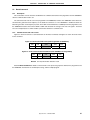
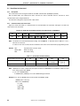

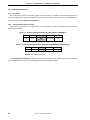


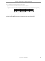


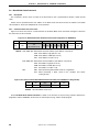
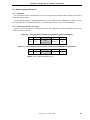
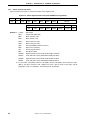


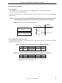


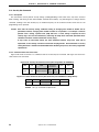
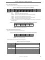


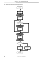
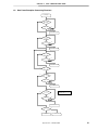

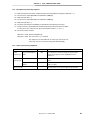
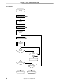
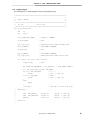


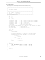


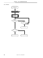


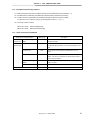


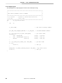
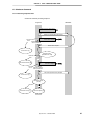

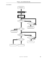


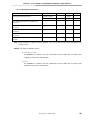
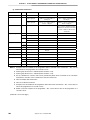


![550 (PDF/57,3Ko) [F]](http://vs1.manualzilla.com/store/data/006354024_1-cb13f59715cefaa4ca521396f0348c03-150x150.png)