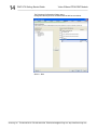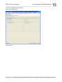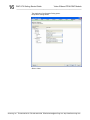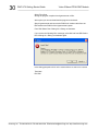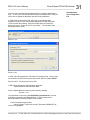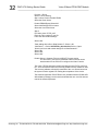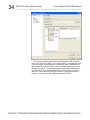
1
Series PMC-VFX70
Virtex-5 Based FPGA
PMC Module
Getting Started Guide
ACROMAG INCORPORATED
30765 South Wixom Road
P.O. BOX 437
Wixom, MI 48393-7037 U.S.A.
[email protected]
Copyright 2009, Acromag, Inc., Printed in the USA.
Data and specifications are subject to change without notice.
Tel: (248) 295-0310
Fax: (248) 624-9234
8500-827-D09F009
2
PMC-VFX Getting Started Guide
Virtex-5 Based FPGA PMC Module
__________________________________________________________________
TABLE OF
CONTENTS
IMPORTANT SAFETY CONSIDERATIONS
You must consider the possible negative effects of power, wiring,
component, sensor, or software failure in the design of any type of
control or monitoring system. This is very important where property
loss or human life is involved. It is important that you perform
satisfactory overall system design and it is agreed between you and
Acromag, that this is your responsibility.
1.0 General Overview
The information of this manual
may change without notice.
Acromag makes no warranty
of any kind with regard to this
material, including, but not
limited to, the implied
warranties of merchantability
and fitness for a particular
purpose. Further, Acromag
assumes no responsibility for
any errors that may appear in
this manual and makes no
commitment to update, or
keep current, the information
contained in this manual. No
part of this manual may be
copied or reproduced in any
form without the prior written
consent of Acromag, Inc.
FPGA Fabric Functions…………..........................…
PowerPC Functions ……...… …… … …… … …. …. .
Bootloop Overview…...………………………….........
DDR Program Overview………………...……….........
DDR Program Download..……………...……….........
DDR Program Execution..……………...……….........
Development Hardware……………………………….
4
5
6
6
6
7
8
2.0 Example Design Creation
New Project Creation...…………...…………………...
Xilinx Platform Studio Base System Builder………
PowerPC MHS File……………………………………..
Compile Design In ISE………………….........………..
Bootloop Program Generation……….........………..
Bootloop Program ……………………..………………
Build Bootloop Program Into Configuration File…
DDR Program Creation………………..………………
DDR PowerPC Program… ……..…………………..…
DDR Binary File Generation ……..………………..…
9
11
18
21
24
26
31
33
35
37
__________________________________________________________________________
Acromag, Inc. Tel:248-295-0310 Fax:248-624-9234 Email:[email protected] http://www.acromag.com
PMC-VFX User’s Manual
Virtex-5 Based FPGA PMC Module
___________________________________________________________________
If you have problems, you should visit the Acromag worldwide web site
at http://www.acromag.com. Our web site contains the most up-to-date
product and software information.
Choose the “Support” hyperlink in our website’s top navigation row then
select “Embedded Board Products Support” or go to
http://www.acromag.com/subb_support.cfm to access:
• Application Notes
• Frequently Asked Questions (FAQ’s)
• Knowledge Base
• Tutorials
• Software Updates/Drivers
An email question can be submitted from within the Knowledge Base or
through the “Contact Us” hyperlink at the top of any web page.
Acromag’s application engineers can also be contacted directly for
technical assistance via telephone or FAX through the numbers listed at the
bottom of this page. When needed, complete repair services are also
available.
The following manuals and part specifications provide the necessary
information for in depth understanding of the board.
Virtex-5 Documentation
IDT70T3519S Spec.
MT47H64M16HR Spec
CY23EP05 Specification
http://www.xilinx.com
http://www.idt.com
http://www.micron.com
http://www.cypress.com
3
WHERE TO GET HELP
www.acromag.com
CAUTION: POWER MUST
BE TURNED OFF
BEFORE REMOVING OR
INSERTING BOARDS
RELATED
PUBLICATIONS
Trademarks are the property
of their respective owners.
__________________________________________________________________________
Acromag, Inc. Tel:248-295-0310 Fax:248-624-9234 Email:[email protected] http://www.acromag.com
4
PMC-VFX Getting Started Guide
Virtex-5 Based FPGA PMC Module
__________________________________________________________________
1.0 GENERAL
OVERVIEW
In this section an overview of the PMC-VFX is presented and the
Acromag example design that the PMC-VFX executes is also described.
The provided PMC-VFX example design can serve as the launching
point from which your custom design can be developed. The first step is to
become familiar with the provided example design.
The PMC-VFX comes preprogrammed with the example design. This
program is stored in a 32Mx8 Flash memory. The 32Mx8 flash memory is a
256 sector memory with the first 128 sectors allocated for storage of the
reprogrammable FPGA program code. The second 128 sectors are
allocated for storage of PowerPC code and data. The PMC-VFX comes
preprogrammed with both FPGA program code and PowerPC program
code.
The reprogrammable FPGA code is defined by both VHDL files and
PowerPC files. All VHDL and Xilinx PowerPC files used to define the
example design are provided in the Engineering Design Kit (EDK).
FPGA Fabric Functions
The main functions controlled by the VHDL include:
•
Local Bus Interface This VHDL logic provides an interface to a
second smaller Virtex 5 FPGA that handles the PCI-X bus interface.
The local bus interface performs with the reprogrammable FPGA
acting as a slave and the PCI-X bus FPGA acting as the master.
The local bus interface has a 32-bit data bus, address lines 21 to 2,
four byte strobe signals, and five additional control signals.
__________________________________________________________________________
Acromag, Inc. Tel:248-295-0310 Fax:248-624-9234 Email:[email protected] http://www.acromag.com
PMC-VFX User’s Manual
Virtex-5 Based FPGA PMC Module
___________________________________________________________________
•
•
•
•
Dual Port SRAM interface (DP_SRAM Component) A 256K x 64bit synchronous dual port SRAM memory is provided. One port
interfaces to the PCI bus, and the other port is directly connected to
the reprogrammable FPGA. This memory supports DMA transfers
when requested by the system or the reprogrammable FPGA.
Front I/O Interface (AXM_D Component) An interface to front of
panal I/O mezzanine modules of various I/O standards is provided
by way of a 150 pin high speed connector. The interface includes
31 differential signal pairs, 29 control signals, 2 clock signals, and
53 power and ground signals.
Rear I/O Interface (RearLVDS Component) The reprogrammable
FPGA is directly connected to 64 pins of the rear P4 connector. The
reprogrammable FPGA I/O to these signals is powered by 2.5 volts
and can perform any 2.5volt standard FPGA I/O.
PowerPC Interface (PowerPC Component and XC5VFX70T
VHDL) Access to the DDR SDRAM and Block RAM address space
from the PCI bus is performed by way of the PLBV46 Master Single
core. The PCI bus transfer of data is implemented using the
following registers: DDR SDRAM Control/Status, DDR SDRAM
Address, DDR SDRAM Read, DDR SDRAM Write, and DDR
SDRAM Mask Registers. These registers are implemented in the
XC5VFX70T VHDL and are described in the PMC-VFX User’s
Manual. Also, a user interface to the PLBV46 Slave Single core
provides PowerPC read access of the Flash Program Code FIFO.
The XC5VFX70T VHDL code executes the move of the PowerPC
program code/data from flash memory starting at address sector
128 to the Flash Program Code FIFO.
The main functions coded in the PowerPC files include:
•
•
•
•
•
•
5
PowerPC Functions
64Mx32-bit DDR2 Memory Controller The DDR2 SDRAM is
directly accessible by the PowerPC. A DDR2 Memory Controller for
the PowerPC 440 Processor Xilinx core implements this interface
between the PowerPC and the DDR memory. The core is
referenced as the PPC440MC core.
64K Byte Block RAM The bootloop program is executed out of this
memory. The bootloop program is preloaded in this Block RAM as
part of the FPGA configuration file. The bootloop program will
automatically execute upon power-up or reconfiguration.
PLBV46 Master Single Core A user interface to the PLBV46
Master Single core provides a bi-directional interface between the
PCI bus and the DDR memory. This core allows read and write of
DDR SDRAM and Block RAM from the PCI bus. The PCI bus is the
master of this interface.
PLBV46 Slave Single Core This core allows PowerPC read
access of the Flash Program Code FIFO. This core also handles
PowerPC write access to the PowerPC_Read_Reg. The
PowerPC_Read_Reg can be read by the PCI bus at PCI bus BAR2
address plus 0x8070.
UART1 This first UART is used to interface to a dumb terminal for
program output display.
UART2 This second UART is provided for additional program
debug and development.
__________________________________________________________________________
Acromag, Inc. Tel:248-295-0310 Fax:248-624-9234 Email:[email protected] http://www.acromag.com
6
PMC-VFX Getting Started Guide
Virtex-5 Based FPGA PMC Module
__________________________________________________________________
Bootloop Overview
DDR Program
Overview
DDR Program
Download
The reprogrammable FPGA example design will run a bootloop out of
the 64K Byte Block RAM after power-up or direct reconfiguration. The
bootloop program will print "Hello World From Block RAM", and then reads
DDR program code from the Flash Program Code FIFO read port and writes
it to DDR memory. The PowerPC reads the Flash Program Code FIFO read
port via PowerPC address 0xFFFE8000. After the data is moved into DDR
memory, the bootloop program will write the Block RAM address
0xFFFFF038 with value 0x33333333. This 0x33333333 value indicates that
the DDR program code has been moved to DDR memory. Next the
bootloop program will set Block RAM address 0xFFFFF030 to 0x33AA33AA
to indicate that it has jumped to address 0x0 in DDR memory to start
execution of the DDR resident program.
The DDR resident example program, provided in file VFX70_DDR.bin,
prints “Hello World From DDR” in a sine wave pattern. After eight sine
waves are printed, the DDR program completes by writing 0x5A5A5A5A to
Block RAM address 0xFFFFF034. Lastly, the DDR program jumps back to
the bootloop program. The bootloop program checks Block RAM address
0xFFFFF034 for the value 0x5A5A5A5A and if found stays in an infinite
while loop. Exit of the while loop and re-execution of the DDR program is
possible by writing 0x0 to Block RAM address 0xFFFFF034.
The DDR2 example program can be downloaded directly into DDR
memory using the PCI bus. The DDR memory example program has the
file name VFX70_DDR.bin. This file can be found on the EDK CD ROM in
the \Designs\PMC_V5\Programmable_FPGA\XC5VFX70T_RevX\VFX70
directory.
The Acromag software is not provided as part of the EDK. It must be
purchased separately. The software available includes Windows DLL
Drivers, VxWorks, QNX, and Linux. The Acromag software provides the
code and drivers that allow exploring and testing the Acromag example
design. For example, the Acromag software has a function that downloads
the VFX70_DDR.bin file into DDR memory.
The Acromag software function that moves the VFX70_DDR.bin file into
DDR memory executes the following.
1) Writes the 32-bit data value that is to be written to the DDR-memory
to the DDR SDRAM Write registers at base address + 8068H.
2) Sets the DDR-SDRAM Mask bits as desired at base address +
806CH. A value of 0H would enable all bytes to be written.
3) Sets the DDR-SDRAM Address register at PCIBAR2 + 8060H with
the DDR-SDRAM write address location. The DDR SDRAM
memory starts at PowerPC base address 0x0. The DDR SDRAM
high address is 0x0FFFFFFF.
4) Issues the Write Command. Set bit-0 of the SDRAM Control/Status
Register at PCIBAR2 + 805CH to logic high.
__________________________________________________________________________
Acromag, Inc. Tel:248-295-0310 Fax:248-624-9234 Email:[email protected] http://www.acromag.com
PMC-VFX User’s Manual
Virtex-5 Based FPGA PMC Module
___________________________________________________________________
After the DDR2 program code has been downloaded into DDR2 memory,
the PowerPC memory space address 0xFFFFF034 must be written with
data pattern 0x0. This will instruct the bootloop program to continue
execution of program code at the first memory location in DDR2 memory. It
does this by jumping to memory location 0x0 in DDR2 memory. The
following is the general procedure for setting memory space address
0xFFFFF034 with the data value 0X0. Note, the DDR SDRAM Read and
Write registers are also used to access the Block RAM memory space in the
PowerPC memory space.
7
DDR Program
Execution
1) Write the 32-bit data value 0X0 to the DDR SDRAM Write registers
at base address + 8068H.
2) Set the DDR-SDRAM Mask bits to 0x0 at base address + 806CH.
3) Set the DDR-SDRAM Address register at PCIBAR2 + 8060H with
0xFFFFF034 the Block RAM write address location. The Block
RAM memory starts at PowerPC base address 0XFFFF0000.
4) Issue the Write Command. Set bit-0 of the SDRAM Control/Status
Register at PCIBAR2 + 805CH to logic high.
After the PowerPC memory space address 0xFFFFF034 is written with
data pattern 0x0, the DDR2 example program executes. The DDR2
program prints the following to the terminal connected to UART port number
one:
"Answer address_Main
"Hello World From DDR2" About eight cycles of a sine wave are
printed.
"-- Exiting main()—"
__________________________________________________________________________
Acromag, Inc. Tel:248-295-0310 Fax:248-624-9234 Email:[email protected] http://www.acromag.com
8
PMC-VFX Getting Started Guide
Virtex-5 Based FPGA PMC Module
__________________________________________________________________
Development
Hardware
To develop and debug PowerPC programs you will need an RS232 Null
Modem Cable and Xilinx JTAG program cable. These cables are directly
connected to the EDK board as shown in the following :
RS232 Null Modem Cable
IMPORTANT: Adequate air
circulation or conduction
cooling must be provided to
prevent a temperature rise
above the maximum
operating temperature.
Connect your RS232 null modem cable from the top left connector of the
EDK board to your hyper-terminal com port. Set the Bit Per Seconds to
9600, Data Bits to 8, Parity to None, and one Stop Bit.
Xilinx JTAG Program Cable
Install the JTAG program cable as recommended by Xilinx. The flat 14
conductor ribbon cable must be connected to the JTAG port of the VFXEDK board as shown in the following figure.
__________________________________________________________________________
Acromag, Inc. Tel:248-295-0310 Fax:248-624-9234 Email:[email protected] http://www.acromag.com
PMC-VFX User’s Manual
Virtex-5 Based FPGA PMC Module
___________________________________________________________________
The development of the Xilinx PMC-VFX project was performed using
the Xilinx ISE Design Suite 11.1 with no service pack. A great deal can be
learned about how the Xilinx ISE, XPS (Xilinx Platform Studio), and SDK
tools are used to develop a custom application by performing the following
project creation procedures. The files provided in the EDK include the
completed project executed in the example design. The steps given in the
following pages will allow one to incrementally develop the project.
1. Make a new directory on your computer (XC5VFX70T_RevD) or copy
the directory structure provided on the EDK CD.
C:\Designs\PMC_V5\Programmable_FPGA\XC5VFX70T_RevD
9
2.0 Example Design
Creation
New Project
Creation
2. Copy the following files
AXM_D.vhd,
DIG_IO_8.vhd,
DP_SRAM.vhd,
RearLVDS.vhd,
v5_sysmon_v1_0.vhd,
XC5VFX70T.vhd,
and XC5VFX70T.Ucf
from the CD-ROM to the new directory XC5VFX70T_RevD.
3. Copy the PMC_VFX70_v2_2_0.xbd and *.ucf files from the EDK CD
ROM \board\Acromag\boards\PMC_VFX70\data folder to
\Xilinx\11.1\EDK\board\Acromag\boards\PMC_VFX70\data folder
4. Copy the pcores folder provided in the EDK CD ROM
edk_user_repository\MyProcessorIPLib folder to
\Xilinx\11.1\edk_user_repository\MyProcessorIPLib folder
5. Start the software by selecting:
Start -> Programs -> Xilinx ISE 11.1 ->ISE-> Project Navigator
6. To create a new project the following steps can be taken. Alternatively,
the project provided on the CD-ROM can serve as a starting point.
7. File -> New Project
Project Name VFX70
Project Location
Give path to VFX70 directory created
C:\Designs\PMC_V5\Programmable_FPGA\XC5VFX70T_RevD
Top-Level source type HDL
Select-> Next
Enter the following Device Properties
Product Category
All
Family
Virtex5
Device
XC5VFX70T
Package
FF1136
Speed Grade
-1
Top-Level Source Type
HDL
Synthesis Tool
XST (VHDL/Verilog)
Simulator
Modelsim-XE VHDL
Preferred Language VHDL
Select ->Enable Enhanced Design Summary
Select-> Next
__________________________________________________________________________
Acromag, Inc. Tel:248-295-0310 Fax:248-624-9234 Email:[email protected] http://www.acromag.com
10
PMC-VFX Getting Started Guide
Virtex-5 Based FPGA PMC Module
__________________________________________________________________
Create New Source Dialog Opens
Select-> Next (no new source are needed)
Add Existing Sources Dialog
Select Add Source button
Browse to the directory location of the .vhd and ucf files you moved in step 2
above.
-> Add Source -> XC5VFX70T.vhd -> Open
-> Add Source -> AXM_D.vhd -> Open
-> Add Source -> DIG_IO_8.vhd -> Open
-> Add Source -> DP_SRAM.vhd -> Open
-> Add Source -> RearLVDS.vhd -> Open
-> Add Source -> v5_sysmon_v1_0.vhd -> Open
-> Add Source -> XC5VFX70T.Ucf -> Open
They should not be copied to project since they already are stored
in the project directory. De-Select the Copy to Project check box.
Select-> Next
Select-> Finish
-> Adding source files -> OK
8. In the Source in Project Dialog Window select
"XC5VFX70T-XC5VFX70T_arch(XC5VFX70T.vhd)" so that it is hi-lighted
9. Add the processor subsystem as a module in the ISE tool.
Select Project -> New Source and then “Embedded Processor” from
the resulting list.
Enter the file name PowerPC.
Select ->Next
Select ->Finish
__________________________________________________________________________
Acromag, Inc. Tel:248-295-0310 Fax:248-624-9234 Email:[email protected] http://www.acromag.com
PMC-VFX User’s Manual
Virtex-5 Based FPGA PMC Module
___________________________________________________________________
This will add an xmp file to the design and launch XPS. In the future
clicking on it will launch XPS (Xilinx Platform Studio). In XPS you can
build the processor system. Exiting XPS leaves you back in ISE, and you
can add your other existing modules to the ISE project just as you would
have previously when there was no embedded processor.
11
Xilinx Platform Studio
Base System Builder
Select ->Yes
Welcome to the Base System Builder! Dialog opens
Select “I would like to create a new design”
Select -> Next
The Board Selection Dialog opens.
Select the down arrow of the Board
Vendor and select Acromag
Select-> Next
__________________________________________________________________________
Acromag, Inc. Tel:248-295-0310 Fax:248-624-9234 Email:[email protected] http://www.acromag.com
12
PMC-VFX Getting Started Guide
Virtex-5 Based FPGA PMC Module
__________________________________________________________________
The System Configuration Dialog opens.
Select Single Processor System
Select -> Next
__________________________________________________________________________
Acromag, Inc. Tel:248-295-0310 Fax:248-624-9234 Email:[email protected] http://www.acromag.com
PMC-VFX User’s Manual
Virtex-5 Based FPGA PMC Module
___________________________________________________________________
13
The Processor Configuration Dialog opens.
Keep all the setting shown.
Select -> Next
__________________________________________________________________________
Acromag, Inc. Tel:248-295-0310 Fax:248-624-9234 Email:[email protected] http://www.acromag.com
14
PMC-VFX Getting Started Guide
Virtex-5 Based FPGA PMC Module
__________________________________________________________________
The Peripheral Configuration Dialog opens.
Change the Memory Size for the Block RAM to 64K as seen below.
Select -> Next
__________________________________________________________________________
Acromag, Inc. Tel:248-295-0310 Fax:248-624-9234 Email:[email protected] http://www.acromag.com
PMC-VFX User’s Manual
Virtex-5 Based FPGA PMC Module
___________________________________________________________________
15
The Cache Configuration Dialog opens.
Keep all the setting shown.
Select -> Next
__________________________________________________________________________
Acromag, Inc. Tel:248-295-0310 Fax:248-624-9234 Email:[email protected] http://www.acromag.com
16
PMC-VFX Getting Started Guide
Virtex-5 Based FPGA PMC Module
__________________________________________________________________
The Application Configuration Dialog opens.
Keep all the setting shown.
Select ->Next
__________________________________________________________________________
Acromag, Inc. Tel:248-295-0310 Fax:248-624-9234 Email:[email protected] http://www.acromag.com
PMC-VFX User’s Manual
Virtex-5 Based FPGA PMC Module
___________________________________________________________________
17
The Summary Dialog opens.
Review the summary of project setting shown in this dialog. Notice the
PowerPC base address assigned to the Block RAM, UARTs, and DDR2
memory, and pcibusif
Select -> Finish
__________________________________________________________________________
Acromag, Inc. Tel:248-295-0310 Fax:248-624-9234 Email:[email protected] http://www.acromag.com
18
PMC-VFX Getting Started Guide
Virtex-5 Based FPGA PMC Module
__________________________________________________________________
In Xilinx Platform Studio window (XPS)
PowerPC MHS
File
Make the following changes to the PowerPC.mhs file.
Double select MHS File: PowerPC.mhs under the Projects Files to open it.
At line 218 of the PowerPC.mhs file replace clk_200_0000MHz with
dcm_clk_s.
The new line 218 should look like the following.
PORT mi_mcclk_200 = dcm_clk_s
Find the BEGIN clock_generator section and comment out lines250 to 253
and also line 263. A line is commented out by placing the # sign at the
beginning of the line. Lines 250 to 253 and 263 should look like the
following.
# PARAMETER C_CLKOUT3_FREQ = 200000000
# PARAMETER C_CLKOUT3_BUF = TRUE
# PARAMETER C_CLKOUT3_PHASE = 0
# PARAMETER C_CLKOUT3_GROUP = PLL0_ADJUST
# PORT CLKOUT3 = clk_200_0000MHz
__________________________________________________________________________
Acromag, Inc. Tel:248-295-0310 Fax:248-624-9234 Email:[email protected] http://www.acromag.com
PMC-VFX User’s Manual
Virtex-5 Based FPGA PMC Module
___________________________________________________________________
19
The PCIBUSIF needs to be added to the bus interface as seen in the Bus
Interface tab
Notice in the PLB bus interface view the box is not filled in. This means that
the pcibusif_0 has not yet been connected to the PLB bus. Select the box
next to MPLB and it will be connected to the PLB bus.
A PLBV46 Master Single custom IP is used to implement an External
Master of the PCI bus. The use of the PLBV46 Master Single IP connects to
the crossbar using a SPLB0/1 interface.
Currently only the MPLB port, where the PPC440 is the master, is aware of
the External Memory connections to DDR. The SPLB0/1 ports require the
MEMCON address ranges to be set to allow PLBV46 Master Single IP to
have access to DDR Memory.
__________________________________________________________________________
Acromag, Inc. Tel:248-295-0310 Fax:248-624-9234 Email:[email protected] http://www.acromag.com
20
PMC-VFX Getting Started Guide
Virtex-5 Based FPGA PMC Module
__________________________________________________________________
In XPS with Project tab and the Bus Interface tab selected right mouse
select on ppc440_0 and select Configure IP.
The ppc440_0:ppc440_virtex5_v1_01_a dialog opens.
Set the base address to 0x00000000 and High Addr to 0FFFFFFF for the
SPLB0 MemCon Range.
Select -> OK
In the MHS file the parameters C_SPLB0_RNG_MC_BASEADDR and
C_SPLB0_RNG_MC_HIGHADDR have been set to the address range as
set above. Lines 72 and 73 of the .mhs file should read as follow:
PARAMETER C_SPLB0_RNG_MC_BASEADDR = 0x00000000
PARAMETER C_SPLB0_RNG_MC_HIGHADDR = 0x0FFFFFFF
__________________________________________________________________________
Acromag, Inc. Tel:248-295-0310 Fax:248-624-9234 Email:[email protected] http://www.acromag.com
PMC-VFX User’s Manual
Virtex-5 Based FPGA PMC Module
___________________________________________________________________
21
The SPLB0 still needs to be connected to the PLB bus. In XPS with the
Project tab selected and the Bus Interface tab selected, select the circle
next to the SPLB0 to make the connection.
File -> Save Project
File -> Exit
The Xilinx Platform Studio (XPS) project has already been instantiated in the
xc5vfx70t.vhd file.
This was done as follows:
•
•
•
Compile Design In
ISE
Select PowerPC in the ISE source tab;
In the processes tab, double select “View HDL Instantiation
Template”
Copy and paste the provided text into the xc5vfx70t.vhd and
connect the ports correctly
The XPS will become a submodule in the ISE project.
The xc5vfx70t.vhd file as provided in the EDK already contains the
PowerPC component Declaration. The component declaration can be found
at lines 407 to 453.
__________________________________________________________________________
Acromag, Inc. Tel:248-295-0310 Fax:248-624-9234 Email:[email protected] http://www.acromag.com
22
PMC-VFX Getting Started Guide
Virtex-5 Based FPGA PMC Module
__________________________________________________________________
The PowerPC instantiation can be found in the xc5vfx70t.vhd file at lines
873 to 917.
In the Processes For Source Dialog Window select:
"Synthesize-XST" so that it is highlighted
Run the compiler by selecting:
Process -> run
In the Processes For Source Dialog Window select:
"Implement Design" so that it is highlighted
Run the compiler by selecting:
Process -> run
In the Processes For Source Dialog Window select:
"Generate Programming File" so that it is highlighted
Process -> Properties
Then select Startup Options tab
FPGA Start-Up Clock
CCLK
Enable Internal Done Pipe
Do not Check
Done (Output Events)
6
Enable Outputs (Output Events) 5
Release Write Enable
5
Release DLL
Default
Match Cycle
Auto
Drive Done Pin High
Check
-> OK
Process -> Properties
Then select Configurations Options tab
Configuration Rate
2
Configuration Pin M0
Pull Down
All other settings remain unchanged
-> OK
Run the Generate Programming File by selecting:
Process -> run
After the design compiles without errors a new program
file can be generated.
In the Processes For Source Dialog Window select:
Under Configure Target Device select:
"Generate Target PROM/ACE File” so that it is highlighted
Process -> Run
In the ISE iMPACT dialog select PROM File Formatter from under the
iMPACT Flows section
Step 1. Select Generic Parallel PROM and then select the Green Arrow
Parallel PROM (Bytes) set to 4M and then select Add Storage Device
Then Select the second Green Arrow
__________________________________________________________________________
Acromag, Inc. Tel:248-295-0310 Fax:248-624-9234 Email:[email protected] http://www.acromag.com
PMC-VFX User’s Manual
Virtex-5 Based FPGA PMC Module
___________________________________________________________________
23
Leave the Checksum Fill Value => FF
File Nave => VFX70
File Location => XC5VFX70T_RevD/VFX70
File Format => MCS
Loading Direction => UP
Number of Data Streams => 1
Data Stream 0 Start Address => 0
Add Data Files => No
Select->OK
“Start adding device file to Data Stream 0” Select-> OK
“Add Device” -> Select XC5VFX70T.bit Select-> Open
“Would you like to add another design file to Data Stream 0?”
Select->No
Select->OK
Select->Operations->Generate File
The file VFX70.mcs is generated, and this file will next be
downloaded over the PCI bus to configure the Virtex-5 device.
Exit without saving.
Select-> No
To configure and run the Virtex 5 PMC-VFX70 board it is recommended that
the Acromag software drivers be used. The Acromag software will simplify
download of the .mcs file and access of the system monitor registers for
reading the temperature of the device. This is a great way to verify initial
functionality of the board. For example, the windows application
PCIVFXDemo.exe (available with the PCISW-API-WIN software package)
can be used to download the new .mcs file and test read of the board
temperature.
The Xilinx JTAG cable will be used to download code to the PowerPC to test
the PowerPC with the developed software.
__________________________________________________________________________
Acromag, Inc. Tel:248-295-0310 Fax:248-624-9234 Email:[email protected] http://www.acromag.com
24
PMC-VFX Getting Started Guide
Virtex-5 Based FPGA PMC Module
__________________________________________________________________
Bootloop Program
Generation
Open Xilinx Platform Studio.
From the Xilinx Platform Studio select
Project-> Export Hardware Design to SDK
Set path to ../XC5VFX70T_RevD/VFX70/PowerPC
Select the Export & Launch SDK Button
Select->OK
Under the File menu Select->Software Platform
__________________________________________________________________________
Acromag, Inc. Tel:248-295-0310 Fax:248-624-9234 Email:[email protected] http://www.acromag.com
PMC-VFX User’s Manual
Virtex-5 Based FPGA PMC Module
___________________________________________________________________
25
Under Project Name: enter ppc440_0_sw_platform
Keep the rest of the dialog defaults
Select-> Finish
Under File menu select New-> Managed Make C Application Project
Enter BootloopPowerPC in the Project Name: edit box
Select Empty Application in the Sample Application section
Select-> Finish
With BootloopPowerPC {ppc440_0_sw_platform} highlighted (selected)
Under File menu select New-> Source File
In the Source File: edit box enter main.c
Select->Finish
In the Editor view, edit the default program “main.c” and save it. This
creates a bootloop program in SDK as an elf application. The program
listed on the following pages can be cut and pasted into the new main.c file.
Select File->Save.
Saving the program compiles it and generates an elf file.
__________________________________________________________________________
Acromag, Inc. Tel:248-295-0310 Fax:248-624-9234 Email:[email protected] http://www.acromag.com
26
PMC-VFX Getting Started Guide
Virtex-5 Based FPGA PMC Module
__________________________________________________________________
BootLoop
Program
In the Editor view, edit the default program “main.c” and save it. This
creates a bootloop program in SDK as an elf application. The program
listed on the following pages can be cut and pasted into the new main.c file.
Select File->Save.
Saving the program compiles it and generates an elf file.
/// BootloopPowerPC bootloop program
#include
#include
#include
#include
#include
#include
#include
"xparameters.h"
"stdio.h"
"xutil.h"
"xstatus.h"
"xbasic_types.h"
"xio.h"
"xio_dcr.h"
int main()
{
print("Hello World From Block RAM\r\n");
/* declare a function pointer */
int (*func_ptr) ();
char String[80];
u32 i, j;
u32 FullCnt, EmptyCnt;
register unsigned int *pter;
register unsigned int *pter3;
long readval;
long DDRvalue;
long flagvalue;
long CodeSize;
// Initialize jump to DDR2 memory register value to zero
pter = (unsigned int*) 0xFFFFF030;
*pter = 0x0;
// Check for Exit of DDR Program Identification value
// If Block RAM address 0xFFFFF034 is set to 0x5A5A5A5A
// then the program in DDR Memory has completed execution.
pter = (unsigned int*) 0xFFFFF034;
if (*pter == 0x5A5A5A5A)
{
print("+T+\r\n");
}
while(*pter == 0x5A5A5A5A)
{
}
-
__________________________________________________________________________
Acromag, Inc. Tel:248-295-0310 Fax:248-624-9234 Email:[email protected] http://www.acromag.com
PMC-VFX User’s Manual
Virtex-5 Based FPGA PMC Module
___________________________________________________________________
27
// 0xFFFFF038 is set with 0x33333333 if Flash code moved to DDR
pter = (unsigned int*) 0xFFFFF038;
if (*pter != 0x33333333)
{
// Start move of Flash program data to DDR Memory
pter3 = (unsigned int*) 0xFFFE8000;
FullCnt=0;
EmptyCnt=0;
DDRvalue = 0;
readval = *pter3;
if ((readval & 0x80000000) == 0x80000000) {FullCnt++;}
if ((readval & 0x40000000) == 0x40000000) {EmptyCnt++;}
while((readval & 0x40000000) == 0x40000000) //Empty FIFO
{ readval = *pter3;
}
DDRvalue |= (readval & 0xFF) << 24;
readval = *pter3;
if ((readval & 0x80000000) == 0x80000000) {FullCnt++;}
if ((readval & 0x40000000) == 0x40000000) {EmptyCnt++;}
while((readval & 0x40000000) == 0x40000000) //Empty FIFO
{ readval = *pter3;
}
DDRvalue |= (readval & 0xFF) << 16;
readval = *pter3;
if ((readval & 0x80000000) == 0x80000000) {FullCnt++;}
if ((readval & 0x40000000) == 0x40000000) {EmptyCnt++;}
while((readval & 0x40000000) == 0x40000000) //Empty FIFO
{ readval = *pter3;
}
DDRvalue |= (readval & 0xFF) << 8;
readval = *pter3;
if ((readval & 0x80000000) == 0x80000000) {FullCnt++;}
if ((readval & 0x40000000) == 0x40000000) {EmptyCnt++;}
while((readval & 0x40000000) == 0x40000000) //Empty FIFO
{ readval = *pter3;
}
DDRvalue |= (readval & 0xFF);
CodeSize = DDRvalue;
for (i = 0; i < CodeSize; i = i + 4) {
DDRvalue = 0;
readval = *pter3;
if ((readval & 0x80000000) == 0x80000000) {FullCnt++;}
if ((readval & 0x40000000) == 0x40000000) {EmptyCnt++;}
if((readval & 0x10000000) == 0x10000000) //Almost Empty
{
sprintf(&String[0],"DDR Address =%x\r\n", i);
//print (String);
}
DDRvalue |= (readval & 0xFF) << 24;
-
__________________________________________________________________________
Acromag, Inc. Tel:248-295-0310 Fax:248-624-9234 Email:[email protected] http://www.acromag.com
28
PMC-VFX Getting Started Guide
Virtex-5 Based FPGA PMC Module
__________________________________________________________________
readval = *pter3;
if ((readval & 0x80000000) == 0x80000000) {FullCnt++;}
if ((readval & 0x40000000) == 0x40000000) {EmptyCnt++;}
if((readval & 0x10000000) == 0x10000000) //Almost Empty
{
sprintf(&String[0],"DDR Address =%x\r\n", i);
//print (String);
}
DDRvalue |= (readval & 0xFF) << 16;
readval = *pter3;
if ((readval & 0x80000000) == 0x80000000) {FullCnt++;}
if ((readval & 0x40000000) == 0x40000000) {EmptyCnt++;}
if((readval & 0x10000000) == 0x10000000) //Almost Empty
{
sprintf(&String[0],"DDR Address =%x\r\n", i);
//print (String);
}
DDRvalue |= (readval & 0xFF) << 8;
readval = *pter3;
if ((readval & 0x80000000) == 0x80000000) {FullCnt++;}
if ((readval & 0x40000000) == 0x40000000) {EmptyCnt++;}
if((readval & 0x10000000) == 0x10000000) //Almost Empty
{
sprintf(&String[0],"DDR Address =%x\r\n", i);
//print (String);
}
DDRvalue |= (readval & 0xFF);
// Write to DDR Memory
pter = (unsigned int*) i;
*pter = DDRvalue;
}
// The FIFO should not become full or empty
sprintf(&String[0],"Full Flag Count =%x\r\n", FullCnt);
print (String);
sprintf(&String[0],"Empty Flag Count =%x\r\n", EmptyCnt);
print (String);
// 0xFFFFF038 is set with 0x33333333 if Flash code moved to DDR
pter = (unsigned int*) 0xFFFFF038;
*pter = 0x33333333;
}
sprintf(&String[0],"Answer =%x\r\n", CodeSize);
print (String);
readval = *pter;
sprintf(&String[0],"Answer =%x\r\n", readval);
print (String);
-
__________________________________________________________________________
Acromag, Inc. Tel:248-295-0310 Fax:248-624-9234 Email:[email protected] http://www.acromag.com
PMC-VFX User’s Manual
Virtex-5 Based FPGA PMC Module
___________________________________________________________________
//
//
//
//
29
Set the pointer address to the Block RAM location used to
check for 0x33AA33AA which indicates that DDR2 memory is loaded
with program code and the bootloop program can now jump to
execute DDR2 program code.
pter = (unsigned int*) 0xFFFFF030;
*pter = 0x33AA33AA;
print("-- Exiting main() --\r\n");
print("\n");
// Jump to DDR resident program in DDR memory at address 0x0
func_ptr = 0x1d0;
func_ptr();
return 0;
}
-
Edit the Linker Script of the program to make sure it will run properly in
hardware from block RAM:
Right select on BootloopPowerPC
Select “Generate Linker Script”
In the Linker Script Generator dialog
Find Assign all Code section to: and select “xps_bram_if_cntlr_1” with the
down arrow.
Find Assign all Data section to: and select “xps_bram_if_cntlr_1” with the
down arrow.
Also assign the heap and stack sections to block RAM.
Select -> Generate
Select -> OK
__________________________________________________________________________
Acromag, Inc. Tel:248-295-0310 Fax:248-624-9234 Email:[email protected] http://www.acromag.com
30
PMC-VFX Getting Started Guide
Virtex-5 Based FPGA PMC Module
__________________________________________________________________
Select File->Save.
Saving the program compiles it and generates an elf file.
At this point you can test download the program to the board.
Setup Hyperterminal and connect the RS232 null modem cable from the
EDK board to the RS232 of the Hyperterminal system.
From SDK Select Run->Debug As-> Debug on Hardware
If you receive the following Error message, select OK and from SDK Select
Run->Debug As-> Debug on Hardware again.
In the debug perspective click on the resume button or select run->resume
Terminate
Exit SDK
__________________________________________________________________________
Acromag, Inc. Tel:248-295-0310 Fax:248-624-9234 Email:[email protected] http://www.acromag.com
PMC-VFX User’s Manual
Virtex-5 Based FPGA PMC Module
___________________________________________________________________
You will need to add the BootloopPowerPC.elf as a software application in
XPS. In XPS you must mark the Block RAM for initialization and in ISE you
will be able to update the bitstream with this elf only application.
31
Build Bootloop
Into Configuration
File
In XPS under the applications tab, right click on the Add Software
Application Project. In the Add Software Application Project dialog that
comes up enter the following: Enter the Project Name as “BootLoop”.
Select box next to “Project is an ELF only Project”. Then browse to the
BootloopPowerPC.elf file.
Select -> Yes
Select -> OK
In XPS, under the Applications Tab find the Project BootLoop. Use the right
mouse button to select BootLoop and then select “Mark to initialize BRAM”.
Exit from XPS. This takes you back to ISE.
In ISE find the Processes Dialog Window and select:
“Update Bitstream with Processor Data”
Run the Update Bitstream with Processor Data by selecting:
Process -> run
This generates a new bit file called XC5VFX70T_download.bit. Use this
new bit file to generate the PROM MSC file. This process puts the
BootloopPowerPC bootloop program in Block RAM.
In the Processes Dialog Window:
under Configure Target Device select "Generate PROM/ACE File"
so that it is highlighted
__________________________________________________________________________
Acromag, Inc. Tel:248-295-0310 Fax:248-624-9234 Email:[email protected] http://www.acromag.com
32
PMC-VFX Getting Started Guide
Virtex-5 Based FPGA PMC Module
__________________________________________________________________
Process -> Rerun
Select-> OK to warning
Step 1 select Generic Parallel PROM
Select the Green Arrow
Parallel PROM (Bytes) Select 4M
Select Add Storage Device button
Select the next Green Arrow
Step 3
File Name enter VFX70_revD
Enter the File Location to your file
Leave the other default settings
Select->OK
“Start adding device file to Data Stream 0” Select-> OK
“Add Device” -> Select XC5VFX70t_download.bit Select-> Open
“Would you like to add another design file to Data Stream 0?”
Select->No
Select->OK
Select->OK
Double Select-> Generate File in the iMPACT Process section
The file VFX70_revD.mcs is generated and this new file can be
downloaded over the PCI bus to configure the Virtex-5 device.
The Virtex 5 FPGA should be reconfigured with the new VFX70_revD.mcs
file. As recommended earlier the Acromag software drivers should be used.
The Acromag software will simplify download of the .mcs file and access of
the system monitor registers for reading the temperature of the device.
The windows application PCIVFXDemo.exe (available with the PCISW-APIWIN software package) can be used to download the new .mcs file and test
read of the board temperature.
__________________________________________________________________________
Acromag, Inc. Tel:248-295-0310 Fax:248-624-9234 Email:[email protected] http://www.acromag.com
PMC-VFX User’s Manual
Virtex-5 Based FPGA PMC Module
___________________________________________________________________
To build a program for download into DDR2 memory from the SDK the
following steps can be followed:
33
DDR Program
Creation
Open Xilinx Platform Studio.
From the Xilinx Platform Studio select
Project-> Export Hardware Design to SDK
Set path to ../XC5VFX70T_RevD/VFX70/PowerPC
Select the Export & Launch SDK Button
Under File menu select New-> Managed Make C Application Project
Enter DDR_PowerPC in the Project Name: edit box
Select Empty Application in the Sample Application section
Select-> Finish
With DDR_PowerPC {ppc440_0_sw_platform} highlighted (selected)
Under File menu select New-> Source File
In the Source File: edit box enter main.c
Select->Finish
From SDK right mouse select the Project name
”DDR_PowerPC{ppc440_0_sw_platform}” from the c/c++ Project panel on
the left.
Select properties.
Select C/C++ Build in the left banner.
Select the Tool Settings tab.
Select Miscellaneous under the PowerPC C Compiler
Enter –nostartfiles in the Other Compiler Options to Append box as seen
on the following page.
Select->OK
__________________________________________________________________________
Acromag, Inc. Tel:248-295-0310 Fax:248-624-9234 Email:[email protected] http://www.acromag.com
34
PMC-VFX Getting Started Guide
Virtex-5 Based FPGA PMC Module
__________________________________________________________________
The Acromag example design DDR resident program, DDR_PowerPC,
prints “Hello World From DDR” in a sine wave pattern. After eight sine wave
cycles are printed, the DDR program completes by writing 0x5A5A5A5A to
Block RAM address 0xFFFFF034. Lastly, the DDR program jumps back to
the bootloop program. The bootloop program checks Block RAM address
0xFFFFF034 for the value 0x5A5A5A5A and if found stays in an infinite
while loop. Exit of the while loop and re-execution of the DDR program is
possible, by writing 0x0 to Block RAM address 0xFFFFF034.
__________________________________________________________________________
Acromag, Inc. Tel:248-295-0310 Fax:248-624-9234 Email:[email protected] http://www.acromag.com
PMC-VFX User’s Manual
Virtex-5 Based FPGA PMC Module
___________________________________________________________________
Cut and paste the following DDR_PowerPC program into main.c
35
DDR PowerPC
Program
// DDR_PowerPC
// Welcome to Xilinx Platform Studio SDK !
#include "xparameters.h"
#include "stdio.h"
#include "xutil.h"
#include "xstatus.h"
#include "xbasic_types.h"
#include "xio.h"
#include "xio_dcr.h"
int main()
{
char String[80];
unsigned int *pter;
Xuint32 address_Main;
address_Main = main;
extern double sin();
double temp;
int count;
int (*func_ptr) ();
sprintf(&String[0],"Answer =%x\r\n", address_Main);
print (String);
// Set Block RAM address 0xFFFFF034 with 0x0 to indicate
// started DDR memory program
pter = (unsigned int*) 0xFFFFF034;
*pter = 0x0;
for(temp = 0.0; temp < 50.0; temp += .25)
{
count = (int)(30+(28*(sin(temp))));
while(count-- > 0)
print(" ");
print("Hello World From DDR2\r\n");
}
// Set Block RAM address 0xFFFFF034 with 0x5A5A5A5A to indicate
// end of DDR memory program
pter = (unsigned int*) 0xFFFFF034;
*pter = 0x5A5A5A5A;
print("-- Exiting DDR main() --\r\n");
print("\n");
// Jump back to bootloop program
func_ptr = 0xFFFF0000;
func_ptr();
return 0;
}
__________________________________________________________________________
Acromag, Inc. Tel:248-295-0310 Fax:248-624-9234 Email:[email protected] http://www.acromag.com
36
PMC-VFX Getting Started Guide
Virtex-5 Based FPGA PMC Module
__________________________________________________________________
Edit the Linker Script of the program to make sure it will run properly in
hardware from DDR memory.
Right select on DDR_PowerPC{ppc440_0_software_platfrom}
Select “Generate Linker Script”
In the Linker Script Generator dialog
assign all Code section to:
Select “DDR2_SDRAM_W1D32M72R8A_5A_C_MEM_BASEADDR”
assign all Data section to:
Select “DDR2_SDRAM_W1D32M72R8A_5A_C_MEM_BASEADDR”
assign all Heap and Stack section to:
Select “DDR2_SDRAM_W1D32M72R8A_5A_C_MEM_BASEADDR”
Select -> Generate
Compile your DDR2 main program DDR_PowerPC by selecting File -> Save
in SDK. The elf file generated must be converted to a binary file for
download into DDR2 memory from the PCI bus or Flash memory. Exit SDK
by selecting File -> Exit.
__________________________________________________________________________
Acromag, Inc. Tel:248-624-1541 Fax:248-624-9234 Email:[email protected] http://www.acromag.com
PMC-VFX User’s Manual
Virtex-5 Based FPGA PMC Module
___________________________________________________________________
The following steps are needed to generate the binary file.
1. Open a DOS command prompt dialog: Start-> All Programs->
Accessories-> Command Prompt
2. Change directories to C:\Xilinx\11.1\EDK\gnu\powerpc-eabi\nt\bin.
This is the location of the Xilinx executable powerpc-eabi-objcopy.
You may also need to find and move cygwin1.dll to this directory.
3. Copy the DDR_PowerPC.elf file to C:\Xilinx\11.1\EDK\gnu\powerpceabi\nt\bin
The DDR_PowerPC.elf can be found at
.\XC5VFX70T_RevD\VFX70\PowerPC\SDK\SDK_Workspace\DDR
_PowerPC\Debug
37
DDR Binary
File Generation
4. Type or cut and paste the following at the dos command line:
powerpc-eabi-objcopy -O binary -j.text -j.init -j.fini -j.rodata -j.data j.got -j.got1 -j.got2 -j.ctors -j.dtors -j.eh_frame -j.jcr j.gcc_except_table -j.sdata -j.sbss -j.tdata -j.tbss DDR_PowerPC.elf
VFX70_DDR.bin
5. The VFX70_DDR.bin file generated is used to download into DDR2
memory from either the PCI bus or flash memory.
6. See your PMC-VFX driver software requirements for the location to
which the VFX70_DDR.bin file must be moved. For example, the
PC software requires this file to be stored at
C:\Program Files\Acromag\PCISW_API_WIN\config_files
The PCIVFXDemo.exe provided with PCISW_API_WIN can be used to
download the VFX70_DDR.bin file into flash starting at sector 128 as
follows.
__________________________________________________________________________
Acromag, Inc. Tel:248-295-0310 Fax:248-624-9234 Email:[email protected] http://www.acromag.com
38
PMC-VFX Getting Started Guide
Virtex-5 Based FPGA PMC Module
__________________________________________________________________
PCIVFX Main Menu
----------------------------------------1. Example design demo instructions
2. Locate/Choose board
3. Attach interrupt callback
4. Toggle PCI interrupts - Disabled
5. Toggle FPGA interrupts - Disabled
6. FPGA configuration
7. Copy PowerPC code file to flash
8. Flash commands
9. Dual-Port SRAM menu
10. DMA transfers
11. Raw memory access
12. Display PCI configuration registers
13. View status information
14. Example design menu
99. Exit
Enter selection: 7
Select PowerPC code file
1. Example code file for VFX70
C:\Program
Files\Acromag\PCISW_API_WIN\config_files\VFX70_DDR.bin
2. Other
Enter selection: 1
Writing file to flash. This may take several minutes...
Complete (54192 code bytes written.)
PCIVFX Main Menu
----------------------------------------1. Example design demo instructions
2. Locate/Choose board
3. Attach interrupt callback
4. Toggle PCI interrupts - Disabled
5. Toggle FPGA interrupts - Disabled
6. FPGA configuration
7. Copy PowerPC code file to flash
8. Flash commands
9. Dual-Port SRAM menu
10. DMA transfers
11. Raw memory access
12. Display PCI configuration registers
13. View status information
14. Example design menu
99. Exit
Enter selection:
Now that the DDR2 program has been moved to flash, the next power-up
cycle or reconfiguration will cause the program to be moved into DDR2
memory and executed.
__________________________________________________________________________
Acromag, Inc. Tel:248-624-1541 Fax:248-624-9234 Email:[email protected] http://www.acromag.com