1
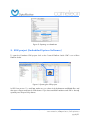
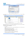
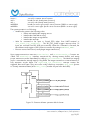
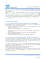
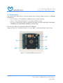
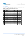
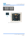
cameleon
FPGA smart camera
Developer Guide v1.2
Cameleon Developer Guide v1.2
Optomotive, mehatronika d.o.o., V Murglah 229, SI-1000 Ljubljana, Slovenia
+386 1 4292914 | [email protected] | www.optomotive.si
page 1/21
1. Introduction
Cameleon is an innovative USB camera based on FPGA system-on-chip (SOC) technology. The
camera with a powerful HSDK (hardware-software development kit) opens ways for rapid
customization and integration of various digital systems into camera itself. The camera is a
readymade solution, but still open for a user to add his own features if he wishes so.
The true power of FPGA (Field Programmable Gate Array) over the sequential microprocessor is
a pipelined parallel data processing. Parallelism reduces system clock and power consumption
considerably while boosting processing power. With the latest set of tools from Xilinx (System
Generator and Accel DSP) you can rapidly develop DSP algorithms even in MathWorks Matlab.
The current integrated image processing is focused on laser line detection (laser triangulation).
The image processing is used to reduce required bus bandwidth which enables usage of multiple
cameras on the same bus.
Key camera features:
• Industrial vision proven CMOS sensor
• Up to 4 sensors per one camera perfectly synchronized
• Can capture video or processed information (profiles)
• Since the image processing is integrated inside the camera the host computer processor is free
for other tasks
• Low cost Xilinx Spartan FPGA
• 64MB (optional 128MB) in-camera buffer
• Up to 127 cameras can be connected to a single USB port (but sharing the bandwidth!)
• Multiple cameras can be synchronized to an external trigger or to a master camera (strobe)
• Firmware (soft-hw and sw) can be upgraded in a minute
• Full source code of the complete system simplifies integration and enables user to customize
the camera to his needs or to train FPGA SOC designing (research and development)
The camera is sold in two basic configurations: MONO (single sensor) or STEREO (dual sensors).
You can upgrade your camera any time by purchasing additional sensor head.
The stereo version is NOT a TRADITIONAL STEREO VISION CAMERA since it does not output
disparity maps! User can add image processing core to add this functionality. The Cameleon
Stereo can only output 2 video streams or processed profiles.
Note: Source code licence is only valid for usage in Optomotive products. Unauthorised usage of
custom cores and supplied software in other commercial products is a violation of licence
agreement and intellectual property (IP) rights. For usage in other products a commercial IP
licences should be obtained. Contact Optomotive for more information ([email protected]).
Cameleon Developer Guide v1.2
Optomotive, mehatronika d.o.o., V Murglah 229, SI-1000 Ljubljana, Slovenia
+386 1 4292914 | [email protected] | www.optomotive.si
page 2/21
2. Building blocks
The camera is composed of a 3 basic parts:
• FPGA System on a module
• Base sensor board
• Head sensor board
All of the vital system components are assembled on a module. This includes power supply,
FPGA, DDR SDRAM, USB controller and SPI Flash (Figure 1). The module is USB powered with
triple DC-DC converters for maximal power efficiency (SMPS - Switching Mode Power Supply in
Figure 1). The core is a Spartan FPGA with DDR SDRAM. The DDR has 16-bit (optional 32-bit)
wide data bus running at 100 MHz offering 400 (optional 800) MB/s peak bandwidth. The
gateway to the PC is a well proven Cypress CY7C68013A (also known as FX2) USB
microcontroller which offers up to 36 MB/s of bandwidth from FPGA to PC in bulk mode. The link
between FPGA and FX2 is 8-bit wide and runs at 48 MHz. The FX2 is also connected to FPGA
through I2C which is used as a command interface. The board also includes non-volatile SPI
FLASH memory. The SPI bus is shared by FPGA and FX2 which is necessary to enable USB
firmware upgrade and FPGA booting. The system board is connected to the base board through
two board-to-board connectors.
Figure 1: Camera structure block scheme
Cameleon Developer Guide v1.2
Optomotive, mehatronika d.o.o., V Murglah 229, SI-1000 Ljubljana, Slovenia
+386 1 4292914 | [email protected] | www.optomotive.si
page 3/21
3. Pre-requisites
Before starting with the camera software modification you need:
• Cameleon camera
• USB cable
• Installation software (downloaded from www.optomotive.si)
• For camera firmware development:
o Xilinx JTAG Download/Debug cable (Platform Cable USB II recommended)
o Xilinx ISE 10.1.03 or higher
o Xilinx EDK 10.1.03 or higher
o Xilinx SDK 10.1.03 or higher
• Recommended also Xilinx Chipscope Pro 10.1 or higher
• Microsoft MS Visual C++ 2008 Express Edition or higher for API DLL development (free
download from www.microsoft.com/express/)
• Qt SDK by Nokia v2009.02 or higher for QtCamera development (free download from
www.qtsoftware.com)
The camera is based on a Trenz Electronic TE0300 Industrial Micromodule. Before proceeding
we recommend to read the module User Manual (http://www.trenz-electronic.de/products/fpgaboards/trenz-electronic/industrial-micromodules.html). It contains important information about
connection the module to debug cable, manual SPI FLASH programming and DIP switches
information. The DIP switches can help you to restore the system if FLASH or EEPROM contain no
valid booting data.
4. EDK project (Embedded System on Chip)
The EDK project is located in #distibution#\ EDK\#project_name_version#.
To open the project and invoke Xilinx Platform Studio (XPS) you have to double click on the
“system.xmp” in project folder in Windows Explorer.
Cameleon Developer Guide v1.2
Optomotive, mehatronika d.o.o., V Murglah 229, SI-1000 Ljubljana, Slovenia
+386 1 4292914 | [email protected] | www.optomotive.si
page 4/21
Figure 2: Opening the EDK project
The system.xmp file is an entry point to any EDK project. It contains information about target
FPGA, custom peripheral depository location and other files location etc. THIS FILE SHOULD
NOT BE MODIFIED BY HAND UNLESS YOU KNOW WHAT YOU ARE DOING! To manage
hardware project use the Xilinx Platform Studio (XMP) instead. The hardware project is defined by
system.mhs (hardware composition) and system.ucf (system signals to external FPGA pinout
mapping). The system.mhs can be edited using the XPS GUI or manually (experienced users). The
system.ucf can only be edited by hand. To edit files by hand simply double click on the filename
in the Project options tab Project.
Cameleon Developer Guide v1.2
Optomotive, mehatronika d.o.o., V Murglah 229, SI-1000 Ljubljana, Slovenia
+386 1 4292914 | [email protected] | www.optomotive.si
page 5/21
Project options
System assembly
Busses
Figure 3: Project in XPS environment
4.1. Hardware system description
The hardware system is basically an embedded system with a Xilinx MicroBlaze 32-bit soft
microprocessor (Figure 4). The MicroBlaze is used to initialize and setup the system. The
horsepower for high bandwidth data streaming is a Multiport Memory Controller (MPMC). Using
a custom built DMA engine (XPS_NPI_DMA) it can stream data from multiple imaging sensors to
external RAM through a MPMC Native Port Interface (NPI). XPS_NPI_DMA can do also
simultaneous data reading to transfer data to USB port at the same time.
This custom built DMA can also rotate (transpose) the images before processing; for example 3D
processing on 90 degrees rotated image. This way we get 752 instead of 480 3D points at
WVGA sensor (57 % more 3D points). Since we get 6 10-bit pixels (64-bit bus) at one
transaction the DMA_FIFOS takes care for proper image line de-multiplexing. The image
processing core XPS_PEAK processes the image line coming from DMA_FIFOS and outputs 32bit 3D point per one image line. The processed data is buffered inside DDR SDRAM and send to
USB through XPS_FX2.
If the rotation and 3D processing is not needed (BASE_clean project) the then XPS_NPI_DMA is
connected directly to XPS_FX2. But this way only 32-bit DMA implementation is possible. When
transferring raw image to USB port the data is transferred directly from DMA engine to XPS_FX2.
The XPS_I2C_SLAVE is used to send commands from the PC to the MicroBlaze - low speed
communication through I2C.
Cameleon Developer Guide v1.2
Optomotive, mehatronika d.o.o., V Murglah 229, SI-1000 Ljubljana, Slovenia
+386 1 4292914 | [email protected] | www.optomotive.si
page 6/21
The XPS_MCH_IIC peripheral is used to communicate with imaging sensors. It has the ability to
send commands to multiple sensors at the same time (different cable lengths are also supported
by using independent sync clock).
The XPS_STEPPER core is used in conjunction with stepper motor driver and takes care for image
synchronous motor rotation. The integrated motor driver core simplifies the system integration. The
XPS_STEPPER core unfortunately does not support acceleration and deceleration. Standard EDK
cores are used to communicate with RS232 (XPS_UARTLITE), SPI FLASH (XPS_SPI)…
Figure 4: Fully featured FPGA system-on-chip architecture
For documentation on specific core (including Optomotive custom cores) right click on the core in
XPS in the System Assembly or in the IP Catalog window. Then select View PDF Datasheet if
available.
Cameleon Developer Guide v1.2
Optomotive, mehatronika d.o.o., V Murglah 229, SI-1000 Ljubljana, Slovenia
+386 1 4292914 | [email protected] | www.optomotive.si
page 7/21
Figure 5: Opening core datasheet
5. SDK project (Embedded System Software)
To open the Cameleon SDK project click on the “Launch Platform Studio SDK” icon in Xilinx
Platform Studio.
Figure 6: Opening the SDK project
In XPS from version 11.x and later make sure you select »Include bitstream and BMM file« and
then press »Export and Launch SDK« button. If you have modified hardware and SDK is already
opened press »Export Only« button.
Cameleon Developer Guide v1.2
Optomotive, mehatronika d.o.o., V Murglah 229, SI-1000 Ljubljana, Slovenia
+386 1 4292914 | [email protected] | www.optomotive.si
page 8/21
Figure 7: Opening the using Export to SDK
To program the camera with hardware and software bitstream click on the »Program FPGA«
button in SDK.
Figure 8: Downloading the hardware and software application to the camera
When using Xilinx SDK v 11.x it is necessary to rebuild software project after major hardware
modifications or moving/copying project to another folder.
Follow this procedure to accomplish this:
• Close SDK
• Delete SDK\SDK_Export\hw (do not delete SDK\SDK_Export\sw since it contains custom
drivers)
• Delete SDK\SDK_Workspace\.metadata
• Delete SDK\SDK_Workspace\microblaze_0_sw_platform
• Click »Export HW design to FPGA« in XPS
• In SDK Menu->File->New->Software Platform...
• Project name »microblaze_0_sw_platform« and press finish
• Import project »cameleon« to workspace: Menu->File->Import
• Click »Existing SDK project into Workspace«
Cameleon Developer Guide v1.2
Optomotive, mehatronika d.o.o., V Murglah 229, SI-1000 Ljubljana, Slovenia
+386 1 4292914 | [email protected] | www.optomotive.si
page 9/21
The other solution is to use external custom cores directory (pcores and drivers).
When using external repository make sure that »Software Repositories« search path is set
properly prior re-compiling project. Select menu Tools->Software Repositories. At »Software
Repositories« window select proper User-Defined Software Repositories by clicking Edit. Select
one directory up (directory EDK) from MyProcessorIPLib which is the actual repository for drivers.
Figure 9: Setting SDK repository search path
We have noticed also one bug which occurs during download »Program FPGA« in SDK. Choose
again proper system.bit, system_bd.bmm and ELF in »Program FPGA« dialog window.
Figure 10: »Program FPGA« dialog window
Press »Save and program«.
If nothing happens for 1minute than kill the process »javaw.exe« in Windows Task Manager.
Cameleon Developer Guide v1.2
Optomotive, mehatronika d.o.o., V Murglah 229, SI-1000 Ljubljana, Slovenia
+386 1 4292914 | [email protected] | www.optomotive.si
page 10/21
Try to rerun »Export HW design to FPGA« in XPS and »Program FPGA« again. If it still does not
work either reset the computer and try again or download bistream using XPS.
The other option which usually works is to download bistream using XPS. Click on »Download
Bitstram to FPGA« botton in XPS.
Figure 11: Downloading merged bitstream using XPS
Just make sure that »Project:cameleon« is marked to initalize BRAM (right click on Software
project). This way XPS takes SDK generated executable (Microblaze software - .ELF) merges it
with hardware bitstream and downloads to FPGA.
5.1. Embedded software description
The SDK project “Cameleon” (#project#\SDK\SDK_Workspace\cameleon) is divided in the
following files:
cameleon.ld
linker script for mapping software to DDR SDRAM
cameleon_bram.ld
linker script for mapping software to internal Block RAM
main.c
source file of main routine
control_fifo.h
header for control FIFO which is used to buffer global commands
control_fifo.c
source for control FIFO which is used to buffer global commands
datatype.h
header for global structure definition OMCAM (all global variables)
dma_func.h
header for DMA functions
dma_func.c
source for DMA functions
func.h
header for commonly used functions
func.c
source for commonly used functions
interrupts.h
header for interrupt routines
interrupts.c
source for interrupt routines
sensors.h
header for common sensor functions
Cameleon Developer Guide v1.2
Optomotive, mehatronika d.o.o., V Murglah 229, SI-1000 Ljubljana, Slovenia
+386 1 4292914 | [email protected] | www.optomotive.si
page 11/21
sensor.c
source for common sensor functions
utils.h
header for utils (mainly timer functions)
utils.c
source for utils (mainly timer functions)
mtXXXXX.h
header for sensor type specific sensor functions (XXXX is a sensor type)
mtXXXXX.c
source for sensor type specific sensor functions (XXXX is a sensor type)
The system operation is as following:
• Initialize the system in the following order:
o Detect and initialize the imaging sensors
o Initialize the OMCAM structure
o Initialize the image storage buffers
o Initialize the interrupts
• Wait for command to be input to Control_FIFO either from UART terminal or
i2c_slave_int_handler(). The XPS_I2C_SLAVE triggers interrupt when 12
bytes are received from FX2 USB microcontroller. When the command is executed, the
Microblaze sends trigger to FX2 USB microcontroller by writing to MB2FX2_REG1.
• Execute received instruction (usually begin image transmission)
Upon image transmission instruction RunPixels() and StartTransfer() function are
called. The RunPixels() initializes transmission by clearing memory buffers and setting
proper transmission mode. Immediately by calling StartTransfer() the data from imaging
sensor is transmitted to internal memory using DMA. The image transmission to internal memory is
fully automatic circular buffer. The captureN_int_handler() interrupt routines are
triggered after each frame. They are used to notify software to increment FIFO_head (pointer
to currently transmitted frame) and FIFO_count (number of bytes left in the buffer).
Figure 12: Camera software operation block scheme
Cameleon Developer Guide v1.2
Optomotive, mehatronika d.o.o., V Murglah 229, SI-1000 Ljubljana, Slovenia
+386 1 4292914 | [email protected] | www.optomotive.si
page 12/21
The main() routine loop constantly checks the image FIFO and FX2 buffer status and sends
data via DMA (pixels_from_ram() routine) to the FX2 if the TX_BUFFER is empty enough
to accept another packet.
If the flag DropFrames=1 then the main loop also throttles the transmission by decimating the
number
of
frames
before
they
reach
the
DMA
by
setting
XPS_IMAGE_CAPTURE_SetFrameDec(). This prevents memory overflow if the USB
cannot transmit all the received frames. With timer and increment value the user can control the
amount of image buffering and therefore a delay between image capture and sending to USB:
if ((2500000 < SysTimer_GetValue())
u16 increment=10;
&& (cam.prop.Mode < 2)) //50ms loop
6. Firmware creation
6.1. For systems executing code from FPGA's block RAM (BRAM)
The Microblaze system has the fastest access to BRAM for code execution. Unfortunatelly this is
limited to 32kB. No caching is necessary for this option.
1. Compile you SW project using a linker script that maps all code to BRAM (usually
included in SDK project).
2. Mark the project to initialize BRAM to be loaded on power-up.
3. Download the bitstream to FPGA (»Program FPGA«) to generate merged bistream to
verify the result.
4. Use \PREPARE_FWU\build_bram_SDK.bat script to generate FIRMWARE.FWU
5. Disconnect JTAG before upgrade!
6. Upload the FIRMWARE.FWU via USB using the USBFirmwareUpgradeTool.
6.2. For systems executing code from DDR SDRAM using bootloader
The Microblaze system can also use DDR SDRAM for code execution. The only limitation in this
case is FLASH size (4MB). Caching is almost necessary for this option for performance issues. But
you need a bootloader to transfer code from FLASH to DDR SDRAM and boot from there. This
procedure has been fully automated using the provided tools.
1. Compile you SW project using a linker script that maps all code to DDR (SDK right click
"Generate linker script"). Remember that Stack and Heap size should be more than 0x800,
otherwise the system migh not work properly.
2. Mark the »bootloader« project to initialize BRAM to be loaded on power-up
3. Download the bitstream to FPGA to generate merged bistream.
4. Use \PREPARE_FWU\copyandbuild_boot.bat script to download everything to FLASH using
JTAG cable or use the generated FIRMWARE.FWU to upload the via USB using the
USBFirmwareUpgradeTool.
Cameleon Developer Guide v1.2
Optomotive, mehatronika d.o.o., V Murglah 229, SI-1000 Ljubljana, Slovenia
+386 1 4292914 | [email protected] | www.optomotive.si
page 13/21
The copyandbuild_boot.bat script copies .bit and .elf file and calls the build_boot.bat. The .bit file
includes bitstream and bootloader executable, while the .elf is a SDRAM executable. The
build_boot.bat accepts both files and SDRAM booting address (usually base address of SDRAM
controller). The script calls several programs in /bin directory and Xilinx installation directory and
does the following steps:
• change the bitstream to MCS
• remove the vectors table from the executable and save as binary
• save vectors table to binary files
• insert header to executable binary using custom program prepare_bootdata.exe
• convert all flash files to MCS and combine in single file
• build flash binary and pack FWU
• burns flash through JTAG at the end if JTAG connection to FPGA is available.
At booting the FPGA is loaded with bitstream which contains bootloader application. The
processor bootloader reads first the header from the FLASH at specified address. In header there
are processor interrupt vectors, number of bytes to read, checksum and booting address. Then it
copies all executable data from FLASH to SDRAM and verifies checksum. After success new
vectors are written to BRAM and application boots from SDRAM.
Cameleon Developer Guide v1.2
Optomotive, mehatronika d.o.o., V Murglah 229, SI-1000 Ljubljana, Slovenia
+386 1 4292914 | [email protected] | www.optomotive.si
page 14/21
7. Connectors
The camera base board has 3 connectors besides mini USB and JTAG connector on TE0300
FPGA board:
• P1 2 x 20 pin1.27 mm header for additional sensor head connection
• P2 2 x 17 pin 2.54 mm header for connection of add-on boards
• P3 5 pin 2.54 mm free pads for industrial USB cable connection (BEFORE ATTACHING
EXTERNAL USB CABLE READ CAREFULLY SECTION 0)
ALL I/O PINS ARE 3.3V LVTLL AND ARE NOT TOLERANT!
Output I/O pins on P1 and ALL I/O pins on P2 are 100Ω serially terminated to reduce noise.
Figure 13: Camera baseboard connectors
Cameleon Developer Guide v1.2
Optomotive, mehatronika d.o.o., V Murglah 229, SI-1000 Ljubljana, Slovenia
+386 1 4292914 | [email protected] | www.optomotive.si
page 15/21
7.1. P1 pinout
The connector P1 is used to connect 40-pin ribbon cable for an additional sensor head. It
contains dual power (5V and 3.3V), 20 I/Os and multiple ground signals for improved noise
immunity. The pin HEAD_RESET_N is currently held static (= 3.3V).
Table 1: Connector P1 pinout
Pin
Name
1
3
5
7
9
11
13
15
17
19
21
23
25
27
29
31
33
35
37
39
HEAD_RESET_N
GND
GND
GND
GND
GND
GND
GND
GND
GND
GND
GND
GND
GND
GND
GND
GND
GND
GND
+5V
Cameleon Developer Guide v1.2
FPGA
FPGA
Name
pin
pin
B14
HEAD_DOUT5
E13
/
HEAD_DOUT6
D13
/
HEAD_DOUT7
E12
/
HEAD_DOUT8
F12
/
HEAD_DOUT9
A12
/
HEAD_LINE_VALID
B11
/
HEAD_FRAME_VALID F11
/
HEAD_DOUT0
D11
/
HEAD_STLN_OUT
A14
/
HEAD_EXPOSURE
A11
/
HEAD_SCLK
E11
/
HEAD_STFRM_OUT
F9
/
HEAD_SDATA
E9
/
HEAD_SYCLK
E10
/
HEAD_PIXCLK
D10
/
HEAD_DOUT1
F8
/
HEAD_DOUT2
E6
/
HEAD_DOUT4
D7
/
HEAD_DOUT3
F7
/
+3.3V
/
Pin
2
4
6
8
10
12
14
16
18
20
22
24
26
28
30
32
34
36
38
40
Optomotive, mehatronika d.o.o., V Murglah 229, SI-1000 Ljubljana, Slovenia
+386 1 4292914 | [email protected] | www.optomotive.si
page 16/21
7.2. P2 pinout
The connector P2 is used to connect additional external peripherals (triggers, UART, stepper
driver, video DAC, PS2…). It contains dual power (5V and 3.3V), 28 I/Os and multiple ground
signals. In the table the pin names in brackets are default pin designations.
Table 2: Connector P2 pinout
Pin
Name
1
3
5
7
9
11
13
15
17
19
21
23
25
27
29
31
33
+5V
GND
EXP0 (UART RX)
EXP2 (TRIG_IN)
EXP4 (STEPR_DIR)
EXP6
EXP8 (STEPR_MS1)
EXP10 (STEPR_RST_N)
EXP12 (DAC_SDATA)
GND
EXP14 (DAC_SCLK)
EXP16
EXP18
EXP20
EXP22
EXP24 (1ST_FRAME0)
EXP26 (TEST_TRIG)
FPGA
FPGA
Name
pin
pin
/
+3.3V
/
/
GND
/
R5
EXP1 (UART TX)
T5
P6
EXP3 (TRIG_OUT)
R6
U4
EXP5 (STEPR_ACK)
V7
V5
EXP7 (STEPR_EN_N)
U5
N7
EXP9 (STEPR_MS0)
U6
R8
EXP11 (STEPR_STEP)
T8
P8
EXP13 (STEPR_HOME)
V9
/
GND
/
N8
EXP15 (STEPR_END)
R11
P10
EXP17
R9
P12
EXP19
N12
V12
EXP21
V13
T12
EXP23
R12
R14
EXP25 (FRM_VALID0)
P13
R13
EXP27 (MB_INT)
U13
Pin
2
4
6
8
10
12
14
16
18
20
22
24
26
28
30
32
34
For UART debug the best option is to use FTDI TTL-232R-3V3 USB to RS232 cable. Connect it to
P2 following this pinout:
FTDI cable
Yellow
Orange
Camera P2
pin6 - EXP1 (UART TX)
pin5 - EXP0 (UART RX)
The UART cable GND is better to leave unconnected to prevent ground loops if using the cable
and camera on the same computer.
Cameleon Developer Guide v1.2
Optomotive, mehatronika d.o.o., V Murglah 229, SI-1000 Ljubljana, Slovenia
+386 1 4292914 | [email protected] | www.optomotive.si
page 17/21
Figure 14: FTDI TTL-232R-3V3 UART cable.
7.3. P3 pinout and connection
The P3 connector is used to connect USB data lines to the USB microcontroller on the TE0300
micromodule. BE CAREFUL WHEN CONNECTING CABLES TO THIS CONNECTOR!
REVERSING POWER POLARITY OR OVER VOLTAGE WILL CAUSE A PREMATURE DEATH OF
THE CAMERA!
Table 3: Connector P3 pinout.
Pin
Name
1
2
3
4
5
+5V (4-6V)
USB DataUSB Data+
GND
CHASIS GND
Standard USB
cable colours
Red
White
Green
Black
SHIELD
Header connector P3 is a 5-pin 2.54 mm (100 mil) pitch connector compatible with the following
industrial USB connectors:
• Bulgin Mini USB Buccaneer PX0443 (IP68 B type Mini USB, front panel mounted, 5 way
crimp connector at rear)
Cameleon Developer Guide v1.2
Optomotive, mehatronika d.o.o., V Murglah 229, SI-1000 Ljubljana, Slovenia
+386 1 4292914 | [email protected] | www.optomotive.si
page 18/21
Figure 15: Bulgin PX0443 (front panel connector).
•
Bulgin Mini USB Buccaneer PX0446 - recommended (IP68 B type Mini USB, rear panel
mounted, 5 way header connector at rear)
Figure 16: Bulgin PX0446 (rear panel connector).
Before connecting the USB to P3 the PCB modifications should be made according to following
table and the two figures as a reference. ONLY SKILLED WORKERS SHOULD DO THE
SOLDERING! TOO LONG SOLDERING OR TOO HOT TIP MAY DAMAGE THE PCB. TO
REMOVE THE SHORT CIRCUIT WE RECOMMEND USING DESOLDERING WICK (BRAID).
Be careful to look at the pictures for correct board revision!
Cameleon Developer Guide v1.2
Optomotive, mehatronika d.o.o., V Murglah 229, SI-1000 Ljubljana, Slovenia
+386 1 4292914 | [email protected] | www.optomotive.si
page 19/21
Table 4: PCB modifications for using P3 connector.
Pin
R3
R4
R5
R6
Mini USB
open
short
open
open
P3 used
short
open
short
short
Figure 17: PCB modification top (board revision 1).
Cameleon Developer Guide v1.2
Optomotive, mehatronika d.o.o., V Murglah 229, SI-1000 Ljubljana, Slovenia
+386 1 4292914 | [email protected] | www.optomotive.si
page 20/21
Figure 18: PCB modification bottom (board revision 1).
Figure 19: PCB modification only on bottom (board revision 1.2).
8. Revision hi story
Rev
Date
Author
1.0 15.5.2009
AG
1.1 27.4.2010
AG
1.2
3.8.2010
AG
Cameleon Developer Guide v1.2
Description
created
Added images for board revision 1.2
Updated to Xilinx tools v12 and added
system description
Optomotive, mehatronika d.o.o., V Murglah 229, SI-1000 Ljubljana, Slovenia
+386 1 4292914 | [email protected] | www.optomotive.si
page 21/21