1
lektronik
abor
Laboratory 1:
Analog Systems of 1. and 2. Order
Prof. Dr. Martin J. W. Schubert
Electronics Laboratory
Regensburg University of Applied Sciences
Regensburg
M. Schubert
Lab1: Analog Systems of 1. and 2. Order
Regensburg University of Applied Sciences
Abstract. Electronic control loop circuits as typical e.g. for ΔΣ A/D
converters are compared to generalized first and second order models
and verified by both simulation and measurement.
1 Introduction
Any system that can oscillate is of at least second order, i.e. it has at least two memories. The
order of a model is the maximum of poles or zeros in its transfer function. As higher order
systems are difficult to treat by analytical calculus, second order system considerations are
popular. They apply to higher order system models also, when the first two poles are
significantly lower than the rest of poles and zeros.
How to work through this laboratory [1]:
• There is no need to fully understand the theory in section 2 to benefit from this tutorial. For
theory it is enough to study the model summary in Fig. subsection 2.3. An in-depth
mathematical derivation of the models is given in [2].
• The Spice [3] simulations of section 3 are useful but no precondition for the hands-on
training. They can be made with a personal computer running the free LTspice simulator.
Fill the “simulated” fields of the tables in chapter 5. Respective LTspice [4] input files [5]
are given on the web together with this documentation.
• During the hands-on training concentrate on section 4 working with the Bode 100 network
analyzer [6],[7], [8]. Fill the "measured" fields of the tables in chapter 5.
The organization of this laboratory is as follows: Section 2 presents theoretical background
according to [2], sections 3 and 4 offer simulation and experimental verification, respectively.
Section 5 contains tables common to sections 3 and 4. In section 6 you can check your
understanding of the fundamental goals of this laboratory. Section 7 draws relevant
conclusion.
-2-
M. Schubert
Lab1: Analog Systems of 1. and 2. Order
Regensburg University of Applied Sciences
2 Theory
Typically the biasing voltage UB is ≠0V. In this case we use a mathematical trick :
Calculate with:
After Solution:
(2.1)
(2.2)
U' = U – UB
U = U' + UB.
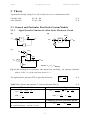
2.1 General and Particular First Order System Models
2.1.1
Signal Transfer Function of a First Order Electronic Circuit
(b)
(a)
Error
X
Uerr1
A
Y
−ω1
s
Uin
Uout
b1
k
(c)
OA1
0V
Uerr1
U'in
C1
R1
U'out1
Rb1
U'out
Caption: U'x = Ux - UBiasing
Fig. 2.1.1-1: (a) High-level schematics, (b) depicted for modeling, (c) OpAmp realization
with ω1=1/R1C1, b1=R1/Rb1 and error source Uerr1.
The signal transfer function (STF) is generally defined as
STF =
U 'out
U 'in
(2.3)
Table 2.1.1: General and particular 1st order model taken from [2]
(a) General 1st Order Model
STF1 =
'
U out
U in'
with s ' =
=
(2.4)
(b) Particular Model of Fig. 2.1.1-1(b)
A0ω 0
A
= 0
s + ω 0 s '+1
STF1 = −
s
ω1
with b1 =
ω0
s →0
⎯⎯⎯→ −
s + b1ω1
R1
Rb1
R
1
= − b1
b1
R1
, ω1 =
,
1
R1C1
(c) Mapping general to particular param.
A1: amplification at ω=0,
A0 = −
ω0: cutoff frequency, used in s'=s/ω0
-3-
Rb1
R1
,
ω0 =
1
Rb1C1
M. Schubert
Lab1: Analog Systems of 1. and 2. Order
Regensburg University of Applied Sciences
Table 2.2.1(a) with parameters A0 and ω0. They are chosen such, that both parameter affect
one single aspect of the circuit only: A0 is the DC amplification and ω0 the cutoff frequency
as shown in Fig. 2.1.1-2 below. Any model – electrical, mechanical, fluid, etc. – with a single
pole only (to be considered) can be described with this general model.
Table 2.1.1(b) shows the transfer function of the circuit in Fig. 2.1.1-1(b).
Table 2.1.1(c) maps the particular parameters of (b) to the general model parameters of (a).
(a)
Fig. 2.1.1-2: First Order System:
(a) Magnitude and
(b) Phase diagram
A0
-3db
lSTFl
dB
0
The pole can be identified by its -45°
phase shift
(b)
ωp=ω0
ωT
log ω
180
135
ωp
10
10 ω p
90
Goal: Find two particular parameters that effect one of the two general parameters only:
1. Which device parameter in Fig. 2.1.1-1(c) affects DC amplification A0 and not pole ω0 ?
....R1....
2. Which device parameter in Fig. 2.1.1-1(c) affects pole ω0 and not DC amplification A0 ?
....C1....
3. What is the DC amplification A0 as f(Rx,C1) ?
A0 =
-Rb1/R1
4. What is the cutoff frequency ω0 as f(Rx,C1) ?
f0 =
1/(2πRb1C1)
-4-
M. Schubert
Lab1: Analog Systems of 1. and 2. Order
2.1.2
Regensburg University of Applied Sciences
Noise Transfer Function
The noise transfer function (NTF) is generally defined as
NTF =
U 'out
U 'err
(2.5)
From noise source Uerr1 we measure at the output U'out=NTF⋅Uerr1. Take the NTF from [2] or
compute it from STF by translating Uerr1 into an equivalent input signal: Divide it by (ω1/s)
and multiply with STF:
NTF1 =
sRb1C1
s
s →0
=
⎯⎯⎯→ 0
s + b1ω1 1 + sRb1C1
(2.6)
Important (e.g. for ΔΣ modulators [9], [10], [11]): Low frequencies are suppressed
proportional to s and therefore particularly for low frequencies.
2.1.3
Stability
There is a single pole in the negative s-plane. It is sp = -b1⋅ω1
Consequence: (Check the correct statement):
The system is
X always stable
O stability depends on device parameters.
-5-
M. Schubert
Lab1: Analog Systems of 1. and 2. Order
Regensburg University of Applied Sciences
2.2 General and Particular Second Order System Models
2.2.1
Signal Transfer Function of a Second Order Electronic Circuit
E
Error
X
2
Y
Y
X
-b2
b1
Fig. 2.2.1: (a) High-level schematics, (b) depicted for modeling, (c) Realization with
ω1=1/R1C1, ω2=1/R2C2, b1=R1/Rb1 , b2=R2/Rb2 and error source Uerr1.
A0, ω0, D are a set of parameters describing the general 2nd order model. They are chosen
such, that any of these parameters affects one aspect of the circuit only: A0 is the DC
amplification, ω0 the cutoff frequency and D adjusts the stability.
Goal: Find three particular parameters that effect one of the three general parameters only:
1. Which device parameter in Fig. 2.2.1(c) affects DC amplification. A0 only? ....R2....
2. Which device parameter in Fig. 2.2.1(c) affects stability Parameter D only? ....Rb1....
3. Which two parameter Fig. 2.2.1(c) affects the cutoff frequency ω0 only?
C1 C2 while C2/C1 keeps constant: C1 =C10⋅cr, C2=C20⋅cr
..............................................................
Further questions important to understand the circuit:
4. What is the DC amplification A1 of the amplifier stage with index 1?
..-Rb1/R1..
5. What is the DC amplification A2 of the amplifier stage with index 2?
...A0/A1..
-6-
M. Schubert
Lab1: Analog Systems of 1. and 2. Order
Regensburg University of Applied Sciences
6. Compute phase and magnitude of STF2(s=jω0). (Hint: It is easiest to compute STF2,general(s'=j).)
.
(2.7)
A0
A0
A0
A
A
= 2
=
= − j 0 = 0 e− j 90°
2D 2D
s ' +2 Ds '+1 j + 2 Dj + 1 − 1 + 2 Dj + 1
STF2, general ( s ' = j ) =
2
Table 2.2.1: General and particular 2nd order model taken from [2]
(a) General 2nd Order Model
STF2, general =
s' =
s
ω0
(b) Particular Model of Fig. 2.1
A0
A0ω02
= 2
s ' +2 Ds'+1 s + 2 Dω0 s + ω02
STF2, particular =
2
: frequency normalized to ω0
with ω x =
d : attenuation / time, dimension: 1/time
d
ω0
U out1 ( s )
ω1ω 2
= 2
U in ( s )
s + b1ω1 s + b2ω1ω 2
A0 =
A0 : amplification at ω=0,
D=
(2.8)
1 Rb 2
=
b2 R 2
1
,
Rx C x
bx =
Rx
,
Rbx
(x=1,2)
: attenuation / wave, dimensionless
ω0 = b2ω1ω 2 =
ω0 : cutoff frequency, used in s'=s/ω0
1
R1C1 Rb 2C2
Poles of the 2. order system:
s p1, 2
⎧ ⎛
2
⎞
⎪ ω 0 ⎜⎝ − D ± D − 1 ⎟⎠ if
=⎨
⎪ω 0 ⎛⎜ − D ± j 1 − D 2 ⎞⎟ if
⎠
⎩ ⎝
2.2.2
D ≥1
D=
D <1
R1 Rb 2
b1ω1
=
2ω0
2 Rb1
C2
C1
Noise Transfer Function of the 2nd-Order System
From noise source Uerr1 we measure at the output U'out=NTF1⋅Uerr1. To compute NTF2 from
STF we translate Uerr1 into an equivalent input signal by dividing it by ω1ω2/s2 and then
multiply with the STF:
NTF2 (U err1 ) =
STF2
ω1ω 2
s2
=
ω1ω 2
s2
s →0
=
−
⎯⎯⎯→ 0
2
2
ω1ω 2 s + ω k1s + ω1ω k 2
s + ω k1 s + ω1ω k 2
s2
(2.9)
From noise source Uerr2 we measure at the output U'out=NTF3⋅Uerr2. To compute NTF3 from
STF we translate Uerr2 into an equivalent input signal by dividing it by ω2/s and then multiply
with the STF:
NTF3 (U err 2 ) =
STF2
ω2
=−
ω1ω 2
s ⋅ ω1
s →0
=− 2
⎯⎯⎯→ 0
ω 2 s + ω k1s + ω1ω k 2
s + ω k1 s + ω1ω k 2
s
2
s
Important (e.g. for ΔΣ modulators): Low frequencies are suppressed proportional to s2.
-7-
(2.10)
M. Schubert
Lab1: Analog Systems of 1. and 2. Order
2.2.3
Regensburg University of Applied Sciences
Stability Investigation Considering the System’s Poles
From (2.8) we know:
Knowing ω 0
D=
1
=
R1C1 Rb 2 C 2
b1ω1
2ω 0
Ù b1 = 2 D
and Rb1 =
R1 Rb 2
2D
ω0
ω1
C2
C1
(2.11)
from (2.8) we can compute the aperiodic
(dead-beat) limit case using D=1 and derive the other cases from it (see table below).
Table 2.2.3: Controlling stability with parameter D for R1=R2=Rb2=100KΩ and C1=C2.
Case
D
=> b1 (ω0/ω1)
=> Rb1 (DevParam)
creep
D>1
b1,creep > 2ω 0 / ω1
Rb1,aper < Rb1,db lim
dead-beat (=aperiodic) limit:
D=1
b1,db lim = 2
ω0
ω1
D = 1/ 2
b1, BW = 2
ω0
ω1
Butterworth:
Phase margin 45°
Ideal oscillator:
Rb1,db lim =
R1 Rb 2
2
(2.12)
Rb1 / KΩ
< 50
C2
C1
50
70.71
Rb1,BW = Rb1,db lim ⋅ 2
1/2
b1, PM 45° = ω 0 / ω1
Rb1, PM 45° = Rb1,db lim ⋅ 2
100
D=0
b1,osc = 0
Rb1 → ∞
∞
Fill the last column in the table above such that it computes the value of Rb1 for
R1=R2=Rb2=100KΩ and C1=C2=220pF.
Consequence: The system is
(a) Pole Locus in the
s=σ+jω plane
jωo
A(1-espt)
4.29%
A
Butterworth
s'p1
45°
Butterworth
(b) Step Response
β
spa
aperiodic
(dead-beat)
limit-case
X stability depends on device parameters.
jω
sp1
s'p2
O always stable
A(1-espat)
σ
sp2
A(1-es'p1t)
-jωo
0
Fig. 2.2.3: (a) Locus of poles in the s-plane and (b) respective step responses
-8-
time
M. Schubert
Lab1: Analog Systems of 1. and 2. Order
Regensburg University of Applied Sciences
2.3 Model Summary
OA2
0V
OA1
0V
U'in
Uerr1
(1st order)
C2
OUT2
R2
U'in
(2nd
order)
(c)
C1
OUT1
R1
Rb2
OUT
U'out
Rb1
-1
Fig. 2.3: 1st and 2nd order system, depending on switch S.
Table 2.3-1: Summary of 1st and 2nd order models and parameters
Property
Signal Transfer
Function, s'=s/ω0
Signal Transfer
Function using
Noise Transfer
Function
DC amplification
System bandwidth /
cutoff frequency
Stability control
parameter
(2.14)
Parameter
1st Order Model
2nd Order Model
STF(s')
A0
s '+1
STF(s)
A0ω0
s + ω0
s 2 + 2 Dω0 s + ω02
NTF(s)
s
→0
STF = ⎯s⎯
⎯→ 0
R1C1
s2
→0
STF ⎯s⎯
⎯→ 0
R1C 2 R1C 2
A0
Rb1
R1
Rb 2
R2
1
2πRb1C1
1
f0
A0
2
s ' +2 Ds'+1
A0ω02
2π R1C1 Rb 2 C 2
R1 Rb 2
D
2 Rb1
C2
C1
Table 2.3-2: Controlling 2nd order system stability for R1=R2=Rb2=100KΩ and C1=C2.
Case
creep
D
D >1
dead-beat (=aperiodic) limit:
D =1
=> Rb1 =f(DevParam)
Rk1,aper < Rb1,db lim
Rb1,db lim =
R1 Rb 2
2
C2
C1
Rb1 / KΩ
< 50
50
1/ 2
Rb1,BW = Rb1,db lim ⋅ 2
70.71
Phase margin 45°
1/2
Rb1, PM 45° = Rb1,db lim ⋅ 2
100
Ideal oscillator:
D=0
Rb1 → ∞
∞
Butterworth:
-9-
(2.15)
M. Schubert
Lab1: Analog Systems of 1. and 2. Order
Regensburg University of Applied Sciences
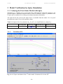
3 Model Verification by Spice Simulation
3.1 Verifying the First-Order Model with Spice
Simulation is a valuable tool to proof and better understand the analytical calculus in the
previous chapter. Nowadays many derivatives of the UC Berkeley’s Spice [3] simulator exist.
LTspice [4] is available free of charge and without simulation limitations.
The input file for the circuit in the figure above is available from the author. Use it to proof
the analytical results. First of all summarize them:
Table 3.1: Impact of device parameters Rb1 R1 and C1 on Amplification A1 and pole fp.
DC ampl. A0
Device parameter:
3.1.1
-Rb1/R1
cutoff frequ. f0 adjust A0 only by adjust f0 only by
1/(2πRb1C1)
R1
Variation of R1
Fig. 3.1.1: LTspice simulation of the 1st-order model: Variation of R1 for the STF.
- 10 -
C1
M. Schubert
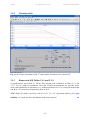
3.1.2
Lab1: Analog Systems of 1. and 2. Order
Regensburg University of Applied Sciences
Variation of Rb1
Fig. 3.1.2: LTspice simulation of the 1st-order model: Variation of Rb1 for the STF.
3.1.3
Homework: Fill Tables 5.1-1 and 5.1-2.
To quantitatively proof table 3.1 fill the lines labeled with "simulated" in tables 5.1-1 and
5.1-2. Use AC mode for simulation. Note that LTspice-measurements are typically better
done with constant device parameters (i.e. without parameter list). Use a cursor to measure A1
and fp at –45° phase drop compared to phase at f=0.
NTF1: In the AC mode: vary R1 by a list at Uin=0V, Uerr1=1V. Agreement with Eq. (2.6)? yes
Stability: AC mode: are there oscillations in the step response?
- 11 -
no
M. Schubert
Lab1: Analog Systems of 1. and 2. Order
Regensburg University of Applied Sciences
3.2 Verifying the Second-Order Model with Spice
Fig. 3.2: LTspice simulation of the second-order model, here: variation of Rb1.
The input file for the circuit in the figure above is available from the author. Use it to proof
the analytical results. First of all summarize them:
Table 3.2: Impact of device parameters Rb1 , R2 , cr on DC-ampl. A0 , D and cutoff frequ. f0.
DC ampl.
model A0
Device
Parameter:
Rk 2
R2
Damping factor
model D
cutoff frequ.
model f0
adjust A0
only by
adjust D
only by
adjust f0
only by
R1 Rk 2
1
R1C1 Rk 2C2
R2
Rb1
cr
D=
2 Rk1
C2
C1
- 12 -
M. Schubert
Lab1: Analog Systems of 1. and 2. Order
Regensburg University of Applied Sciences
Observe the AC-plot in the top part of Fig. 3.2 (colors inverted to save ink). It is the system
A(s)=1/(s'2+2Ds'+1) with s'=ω/ω0 for varying values of D. How can we measure f0=ω0/2π for
different values of D? (Hint: look at the dashed curves, the phase information of the plot.)
Measure f0 at phase = -90°
..............................................................
Vary one after the other the parameters R2, Rb1, cr (with C1=cr⋅C10, C2=cr⋅C20) in the spice
model to proof table 3.2 qualitatively like in Fig. 3.2.
To quantitatively proof table 3.2 fill the lines labeled with "simulated" in tables 5.2-1 and
5.2-2. Use AC mode for simulation. Note that LTspice-measurements are typically better
done with constant device parameters (i.e. without parameter list). Use a cursor to measure
A0, f0, A(f0) at –90° phase drop compared to phase at f=0.
NTF2: Settings: AC mode, Uin=0V, Uerr2=0V, Uerr1=1V.
Does the result agree with Eq. (2.9)? yes What is the slope of Uout(f<f0)?
40
dB/dec
NTF3: Settings: AC mode, Uin=0V, Uerr2=1V, Uerr1=0V.
Does the result agree with Eq. (2.10)? yes What is the slope of Uout(f<f0)?
20 dB/dec
Stability: Oscillations in the step response oscillate at ωp=Im{sp}. What is its model?
fp.=ωp/2π with ωp = ω0⋅ 1 − D 2 for D≤1 (creep case if D>1)
..............................................................
A0
. (Hint: s'=j when ω=ω0.)
2D
Important consequence: At f=f0 here will always be a –90° phase shift.
Proof, that A( f 0 ) = − j
STF2,general(s') =
A0
2
s ' +2 Ds'+1
=
A0
2
j + 2 Dj + 1
=
A0
A
=−j 0
2 Dj
2D
..............................................................
- 13 -
M. Schubert
Lab1: Analog Systems of 1. and 2. Order
Regensburg University of Applied Sciences
4 Experimental Verification of 1st and 2nd Order Model
To get started with the BODE100 Vector Network Analyzer for this laboratory refer to [8].
4.1 First-Order System Characterization
Osci / CH2
Osci / CH1
BODE100 /
OUTPUT
B-WIT
100
R0
1M Ω
50Ω
Fig. 4.1: First Order System Configuration
Caption:
2 mm banana,
4 mm banana,
BNC
Preparing the Board: Setup & Calibration:
Disconnect TRS*) connector from the computer’s sound card. (Speakers may be connected.)
• Verify VDD=3.3V,
• Adjust the IN1+ inputs of the OpAmp OA1 to VB=VDD/2.
• Set Uerr1 = 0V using short circuit
• Disconnect the output of OA2 from Uin1 (i.e. 'Uerr2' is a break) and connect Uin1 to Uin2.
• Set Rb1 = R1 = 100KΩ, C1 = 220pF
Preparing the Oscilloscope: Let’s Use Following Default Settings
• Oscilloscope’s CH1 shows the boards input voltage Uin.
• Oscilloscope’s CH2 shows the boards input voltage Uout.
• Trigger channel CH1.
- 14 -
M. Schubert
Lab1: Analog Systems of 1. and 2. Order
Regensburg University of Applied Sciences
Preparing Bode 100 for Gain/Phase mode mesurements:
• Bode Analyzer Suite Toolbar: Configuration → Device Configuration → set switch right,
connecting Receiver 1 to CH1. Then shorten CH1 to OUTPUT externally with a BNC
cable.
• Click the Gain/Phase toolbar button .
• Source Frequency: 100Hz, Level: 0dB, Attenuators: 20dB, Receiver Bandwidth: 100Hz.
• Connect (a) Bode 100’s OUTPUT and CH1 and the board’s Uin, (b) CH2 to board’s Uout.
• Click the Continuous Measurement
or Single Measurement,
button to measure.
Train in the Gain/Phase mode the settings of OUPUT Level and Attenuators. In the
Frequency Sweep mode things may happen too fast to observe.
Constant parameters below: C1=220pF, Rb1=100KΩ
R1 = Rb1 = 100KΩ: (Results in integral multiples of 10dB.)
1. Set Bode 100’s OUTPUT such, that OA1’s output is max. & sinusoidal Level =
0
dB
2. Adjust Attenuator CH1 such, that CH1 is well loaded. Attenuator
CH1 =
20
dB
3. Adjust Attenuator CH2 such, that CH2 is well loaded. Attenuator
CH2 =
20
dB
Note your measurements:
Mag (dB): ...38 mdB...
Phase (°): ....179...
R1 = 1MΩ: (Results in integral multiples of 10dB.)
4. Set Bode 100’s OUTPUT such, that OA1’s output is max. & sinusoidal Level =
13
dB
5. Adjust Attenuator CH1 such, that CH1 is well loaded. Attenuator
CH1 =
30
dB
6. Adjust Attenuator CH2 such, that CH2 is well loaded. Attenuator
CH2 =
10
dB
Note your measurements:
Mag (dB): ...-20 dB....
Phase (°): ....-180....
R1 = 10KΩ: (Results in integral multiples of 10dB.)
7. Set Bode 100’s OUTPUT such, that OA1’s output is max. & sinusoidal Level = -20
dB
8. Adjust Attenuator CH1 such, that CH1 is well loaded. Attenuator
CH1 =
0
dB
9. Adjust Attenuator CH2 such, that CH2 is well loaded. Attenuator
CH2 =
20
dB
Note your measurements:
Mag (dB): ....19.8....
Phase (°): ....172....
Keep in mind for the following measurements, that Bode 100’s OUTPUT Level must be
adjusted proportional 1/A0.=R1/Rb1! Eventually peaking around f0 must be respected, too.
Bode 100, Frequency Sweep mode:
Click toolbar button
to switch to the Frequency Sweep mode.
Freq.: 100Hz-1MHz, Log. 201 Points, Receiver Bandwidth 100Hz, Level+Attn. optimized.
Activate: Trace 2, Measurement: Gain, Display: Data, Format: Phase (°).
Check → Configuration and → Calibration. Everything ok? Let’s start the measurements!
- 15 -
M. Schubert
Lab1: Analog Systems of 1. and 2. Order
Regensburg University of Applied Sciences
STF: Proof the theory of tables 2.2.1 and 2.4 regarding A0 and/or f0 dependencies:
Connect the Line-out TRS*) plug to the speakers, listen to one or two measurements to get a
feeling for measurement duration and speed.
Perform the 8 measurements required to fill tables 5.1-1 and 5.1-2. Observe the Bode100’s
overload indicator and oscilloscope channel CH2. Avoid overloads by setting OUTPUT Level
and Attenuator CH2 properly.
• A0 and f0 for R1=10KΩ, Rb1=100KΩ, C1=220pF, 2.2nF → note results in table 5.1-1
• A0 and f0 for R1=100KΩ, Rb1=100KΩ, C1=220pF, 2.2nF → note results in table 5.1-1
• A0 and f0 for R1=1000KΩ, Rb1=100KΩ, C1=220pF, 2.2nF → note results in table 5.1-1
• A0 and f0 for R1=100KΩ, Rb1=10KΩ,
• A0 and f0 for R1=100KΩ, Rb1=1MΩ,
Conclusion: Rb1 has impact on
X A0
C1=220pF
C1=220pF
X f0 ,
R1 on X A0
→ note results in table 5.1-2
→ note results in table 5.1-2
O f0 ,
C1 on O A0
X f0
NTF: Measuring the Noise Transfer Function
• Uin=0V (attach BNC short circuit or 50Ω to Uin).
• Rb1=100KΩ, R1=10, 100 or 1000KΩ (has no impact)
• Let CH2 connected to Uout as is.
• Feed Bode100’s OUTPUT to Uerr1 using injection transformer B-WIT100 of Omicron Lab.
Perform a frequency sweep, observe: Low frequencies are suppressed with
20
dB/dec.
Measuring the Errors in the Feedback Path
Use the same measurement setup as above but measure Uout1 instead of Uout. Then Uerr1 is
within the feedback path.
Observe:
Low frequencies are suppressed with
0 dB/dec
Conclusions of the frequency-domain measurements:
Errors at the system’s input are amplified by the
Errors at the forward network’s output are amplified by the
Errors at the feedback network’s output are amplified by the
X STF
O STF
X STF
O NTF
X NTF
O NTF
Time-Domain Measurements
Observe stability in the time domain
• R1 = Rb1 = 100KΩ,
• Uin = 1Vpeak-peak, rectangular, 4 KHz from the waveform generator
• Observe Uin1 and Uout at oscilloscope channels CH1, CH2 for C1=220pF and 2.2nF.
Can you observe any voltage overshoot?
No
- 16 -
M. Schubert
Lab1: Analog Systems of 1. and 2. Order
Regensburg University of Applied Sciences
Analog Audio Signal Processing
Remove waveform generator
Connect the board’s line-in TRS*) plug to line-out of the computer’s sound card (green).
Connect the board’s line-out TRS plug to the speakers.
Play some music, switch amplification (A0) & bandwidth (f0) independently**).
Perceive the effects on the sound.
*)
**)
TRS = Tip, Ring, Sleeve, connected to left channel, right channel and ground, respectively.
Care about other students: low volume. Short test times please!
- 17 -
M. Schubert
Lab1: Analog Systems of 1. and 2. Order
Regensburg University of Applied Sciences
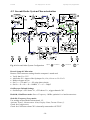
4.2 Second-Order System Characterization
Fig. 4.2: Second Order System Configuration
Caption:
2 mm banana,
4 mm banana,
Board: Setup & Calibration:
Remove TRS connector coming from the computer’s sound card.
• Verify that VDD=3.3V.
• Adjust the IN1+ inputs of the OpAmps OA1, OA2, OA3 to ca. VB=VDD/2.
• Remove bypass of OA2.
• Set Uerr2 = 0V and Uerr1 = 0V using short circuits
• Set Rb1 = R1 = Rb2 = R2 = 100KΩ, C1 = C2 = 200pF
Oscilloscope: Default Settings
• Oscilloscope’s CH1 shows Uin, CH2 shows Uout, trigger channel CH1.
Bode100, Gain/Phase mode: Source Frequency: 100Hz, optimize Level and Attenuations.
Bode100, Frequency Sweep mode:
Use settings as described in subsection 4.1.5.
Activate: Trace 2, Measurement: Gain, Display: Data, Format: Phase (°).
Check for Configuration
Check for Calibration when CH1 is internally connected to OUTPUT.
- 18 -
BNC
M. Schubert
Lab1: Analog Systems of 1. and 2. Order
Regensburg University of Applied Sciences
STF: Proof the theory of tables 2.4-1 and 2.4-2 regarding A0 , f0 , D dependencies:
Perform the 6 measurements to be noted in table 5.3-1. Consider proper settings of OUTPUT
Level and Attenuator CH2 to avoid overloads. Use a cursor to measure f0 at –90° phase drop.
Try also Rb1 > 100KΩ and free oscillation: Rb1→∞ Ù D=0.
Conclusions:
R2 has impact on X A0 O f0 O D,
Rb1 on O A0 O f0 X D,
C1,2 on O A0 X f0 O D
NTF: Measuring the Noise Transfer Function
• Uin=0V (attach BNC short circuit or 50Ω to Uin).
• R2=10, 100 or 1000KΩ (has no impact)
• Let CH2 connected to Uout as is.
• Feed Bode100’s OUTPUT to Uerr1 using injection transformer B-WIT100 of Omicron Lab.
• Perform a frequency sweep.
Observe: Low frequencies are suppressed with
40 dB/dec.
Measuring the Errors in the Feedback Path
• Feed Bode100’s OUTPUT to Uerr3 using injection transformer B-WIT100 of Omicron Lab.
Observe: Amplification at low freq. of the error Uerr3 injected into the feedback path: .0. dB
Conclusions of the frequency-domain measurements:
Errors at the system’s input are amplified by the
Errors at the forward network’s output are amplified by the
Errors at the feedback network’s output are amplified by the
X STF
O STF
X STF
O NTF
X NTF
O NTF
Time-Domain Measurements
(a) Observe stability in the time domain
Set R1=R2=Rb2=100KΩ, Rb1 variable. Remove Bode 100’s OUTPUT from the board’s Uin.
Feed a rectangular waveform with frequency f0/10 (ca. 700Hz) and 1Vpeak-peak to Uin.
Perform the 3 measurements to be noted in table 5.2-2. (1) Dead-beat limit case: Rb1=50KΩ
Ù D=1/2, (2) Butterworth case: Rb1=70KΩ Ù D=1/ 2 , (3) Phase-Margin=45° case:
Rb1=100KΩ Ù D=1. (4) Try also Rb1 > 100KΩ and free oscillation: Rb1→∞ Ù D=0.
(b) Observe stage amplifications in the time domain
Observe the amplification AV2 of the input stage (around OA2) as a function of Rb1! How can
AV2 be modeled as function of A0 and AV1, the amplification of the output stage (around OA1)?
(Hint: The total amplification must be A0 = AV2 AV1 while A0=Rb2/R2 and AV1=-Rb1/R1.)
AV0 and AV1 given
=>
AV2=AV0/AV1.
...............................................................
Analog Audio Signal Processing
•
•
•
•
•
Remove any sources connected to Uin.
Connect the board’s line-in TRS plug to line-out of the computer’s sound card (green).
Connect the board’s line-out TRS plug to the speakers.
Play music, switch stability (D by Rb1) amplification (A0) & bandwidth (f0) independently.
Perceive the effect on the sound, particularly for Rb1→∞ for the different capacitances.
- 19 -
M. Schubert
Lab1: Analog Systems of 1. and 2. Order
Regensburg University of Applied Sciences
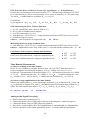
5 Simulated and Experimental Results Summary
5.1 First Order System
Table 5.1-1: Impact of C1 and R1 on Amplification A0 and f0 (= pole fp).
1)
Use a simple resistor for the 1MΩ measurements to avoid parasitic capacitive effects.
R1 →
10 KΩ
100 KΩ
1 MΩ1)
C1 ↓
A0/dB
f0/Hz
A0/dB
f0/Hz
A0/dB
f0/Hz
220 pF
simulated:
measured:
20
20
7210
7010
0
0
7210
7500
-20
-20
7210
7496
2200 pF
simulated:
measured:
20
20
721
737
0
0
721
737
-20
-20
721
737
Table 5.1-2: Impact of Rb1 on Amplification A0 and f0 (= pole fp), constant: R1=100KΩ
10 KΩ
100 KΩ
1000 KΩ
Rb1 →
take val. from above
C1 ↓
check CH2 Overload?
A0/dB
f0/Hz
A0/dB
f0/Hz
A0/dB
f0/Hz
220pF
simulated:
measured:
-20
-20
72100
77254
0
0
7210
7200
20
20
7210
717
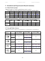
5.2 Second Order System
Table 5.2-1: Parameter’s impact of on Amplification A0, cutoff frequency f0 and stability D.
A0( R2 )
D( Rb1 ) ↓
Rb1=50KΩ,
C1,2=220pF
Rb1=70KΩ,
C1,2=220pF
Rb1=100K,
C1,2=220pF
Rb1=100K,
C1,2=2200pF
10 KΩ
100 KΩ
1000 KΩ
Output level = -20dB
Output level = 0dB
Output level = 10dB
A0/dB, f0/KHz, A(f0)/dB
A0/dB, f0/KHz, A(f0)/dB
A0/dB, f0/KHz, A(f0)/dB
0 , 7.23, -6.01
simulated:
measured:
X
0, 7.20, -5.88
0, 7.23, -3.09
simulated:
measured:
X
X
0, 7.20, -3.07
X
simulated:
20, 7.23, 20.0
0, 7.23, 0
-20, 7.23, -20.0
measured:
20, 7.20, 20
0, 7.20, -0.118
-20, 7.30, -20
0, .724, -0.006
simulated:
measured:
X
0, 747, -0.104
- 20 -
X
M. Schubert
Lab1: Analog Systems of 1. and 2. Order
Regensburg University of Applied Sciences
Table 5.2-2: Stability observations in the time domain: Voltage overshoot and oscill. frequ.
Case
Aperiodic (deadbeat) limit-case
mV
%
Uin = 1V
Butterworth
Phase Margin = 45°
mV
%
mV
%
Uout voltage simulated:
Overshoot:
measured:
0
0
40.5
4.05
163
16.3
0
0
50
5
180
18
Oscillation
frequency:
-
-
as f(f0)
≤ f0, exact: Im{s p1,2 / 2π } = f 0 1 − D 2
6 Check Your Knowledge
Can you resolve acronyms STF and NFT? What is their general definition as function of Uin,
Uerr, Uout? Can you apply these voltages if they are not given? What are the STF1, STF2 and
NTF1, NTF2 for the particular 1st and 2nd order circuits of this laboratory?
Typically circuits are driven with a biasing voltage UB to avoid a second power supply. This
DC-offset is contradictory to the rules of LTI systems [2]. What do we do to get
mathematically rid of UB?
1st order system: What two parameters characterize a very general 1st order STF with DCamplification and a single pole? Which device parameters in our particular circuit have
impact on only one of these general parameters? Tendency of this impact (e.g. lower x →
higher y)? Can this system become instable by parameter variations?
2nd order system: What three parameters characterize a very general 2nd order STF with DCamplification and two poles? Which device parameters in our particular circuit have impact
on only one of these general parameters? Tendency of this impact (e.g. lower x → higher y)?
What stability case is given for general parameter D=1? What case is D=1/ 2 ? How do you
identify these cases in a Bode diagram? Is D=0 more or less stable than D=1 or D→∞?
- 21 -
M. Schubert
Lab1: Analog Systems of 1. and 2. Order
Regensburg University of Applied Sciences
7 Conclusions
Draw your personal conclusions from this laboratory.
The general control loop model combined with the general 1stand 2nd- order system models in the Laplace domain apply well
to 1st- and 2nd- order circuit behavior for both simulation and
measurement.
The
comparison
of
simulated
and
experimental
results is respectable in face of the fact that very simlpy
spice models were used. Particularly the operational amplifiers
were assumed to be near-ideal having neither poles nor zeros,
infinite input and zero output impedance. A better OpAmp macro
should introduce at least two additional poles for every OpAmp.
8 References
[1]
[2]
[3]
[4]
[5]
[6]
[7]
[8]
[9]
[10]
[11]
M. Schubert, Courses at Regensburg University of Applied Sciences. Available: http://homepages.fhregensburg.de/~scm39115/ → Offered Education → Courses and Laboratories
M. Schubert, [1] → Document “Linear Control Loop Theory”.
The Spice Page, EECS Department of the University of California at Berkeley, available:
http://bwrc.eecs.berkeley.edu/Classes/icbook/SPICE/.
LTspice, available: http://www.linear.com/designtools/software/
M. Schubert, [1] → LTSpice Input Files.
Bode 100 User Manual, available http://www.omicron-lab.com/manuals/pdf.html.
Bode 100 Network Analyzer Suite, available http://www.omicron-lab.com/downloads.html.
M. Schubert, [1] → Document "BODE100 Quickstart for Spectrum Analysis".
J. C. Candy, G. C. Temes, 1st paper in “Oversampling Delta-Sigma Data Converters, Theory, Design and
Simulation”, IEEE Press, IEEE Order #: PC0274-1, ISBN 0-87942-285-8, 1991.
S. R. Norsworthy, R. Schreier, G. C. Temes, „Delta-Sigma Data Converters“, IEEE Press, 1996, IEEE
Order Number PC3954, ISBN 0-7803-1045-4.
M. Schubert, [1] → Document "Delta-Sigma Modulation"".
- 22 -