1
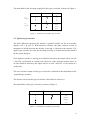
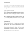
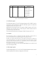
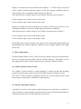
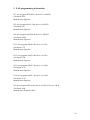
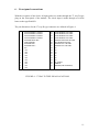
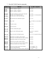
R.G.O.
32 BIT CAMAC COUNTER MODULE
USER MANUAL
C.S. Amos / D.J. Steel
16th August 1993
Copyright © R.G.O. August 1993
1. General description.
3
2. Encoder formats
3
2.1 A quad B type encoders .......................................................... 3
2.2 Up/down type encoders........................................................... 4
3. Reference and clock input signals
5
3.1 Input 1 - Clock ........................................................................ 5
3.2 Input 2 - Zero set marker......................................................... 5
3.3 Input 3 - Encoder zero reference............................................. 5
3.4 Inputs 4,5,6 & 7 - Datum markers .......................................... 5
4. Circuit description
6
4.1 Power on reset......................................................................... 6
4.2 Anti-coincidence and timing circuits ...................................... 6
4.3 LAM status register................................................................. 6
4.4 LAM mask register ................................................................. 7
4.5 Counters .................................................................................. 7
4.6 Data output registers ............................................................... 7
4.7 Data output buffer ................................................................... 8
4.8 Camac function decoder circuit .............................................. 8
4.9 Encoder input phase detector .................................................. 8
4.10. Optically coupled input isolators. ........................................ 9
5. PAL programming information
10
6. Front panel connections
11
7. Decoded CAMAC function commands
12
8. Circuit diagram
13
2
1. General description
The Encoder Counter Module is a 32 Bit binary up/down counter intended to
determine absolute telescope positions from an incremental encoder which may be :- a
rotary optical, linear optical or inductive tape encoder.
The design is based on the 28 bit binary up/down counter designed by RGO and
manufactured by Grubb Parsons. An enhanced version was developed by HYTEC
Electronics using PLD technology to rationalise the circuitry, this also had the benefit
of reducing the size from a triple to a single width module.
The design was further developed by RGO to give 32 bit counts to satisfy the
requirement for the high resolution WHT Azimuth tape encoder experiment.
Features of the new unit are 32 bit counting, C.A.D. design, multi-layer PCB,
configurable encoder input circuitry, clearer front panel display and legend, buffering
of all BUS signals and as before PLD technology.
2. Encoder formats
2.1 A quad B type encoders
A quad B format encoders have two outputs (O/P 1 & O/P 2) which are 90°
electrically displaced and a zero reference output that occurs when the encoder
reaches its reference position (ie. 1 pulse per rev).
In order to determine the direction in which the encoder is rotating, we need to
establish which of the two outputs (O/P 1 or O/P 2) is leading the other. If O/P 1 is
leading, the encoder is rotating in a clockwise direction and the counter needs to
count up. When O/P 2 is leading, the encoder is rotating in an anti-clockwise direction
so the counter needs to count down.
The decoder circuit for this type of encoder is described in section 4.9.
3
The truth table for the decoding required for this type of encoder is shown in Figure 1.
ENCODER O/P 1
O/P 1
ENCODER O/P 2
COUNT
L
UP
UP
H
LEADING
UP
H
UP
L
DOWN
L
O/P 1
LAGGING
DOWN
H
DOWN
H
DOWN
L
Figure 1 - Truth table for a quad b type encoders.
2.2 Up/down type encoders
The basic difference between this and the A quad B encoder are the two encoder
outputs (O/P 1 & O/P 2). With up/down encoders, the phase detector circuit to
determine in which direction the encoder is moving, is internal to the encoder. If A
quad B type encoders are used, the decoding circuitry is external and usually defined
by the system designer.
If the up/down encoder is moving in a clockwise direction, the output will be on O/P
1 and O/P 2 will remain in a steady state. However, if the up/down encoder moves in
an anti-clockwise direction, the output will be on O/P 2 and O/P 1 will remain in a
steady state.
The zero reference output on this type of encoder is identical to that described for the
A quad B type encoders.
The decoder circuit for this type of encoder is described in section 4.9.
The truth table for this type of encoder is shown in Figure 2.
ENCODER O/P 1
ENCODER O/P 2
COUNT
H
UP
L
DOWN
H
DOWN
L
UP
Figure 2 - Truth table for up/down type encoders
4
3. Reference and clock input signals
3.1 Input 1 - Clock
The clock input is a pulse train of 1 μSec wide pulses at a frequency of 20 Hz and is
the rate at which the telescope computer system (TCS) samples data. This signal is
derived from the observatory Time Service’s and is used to transfer the contents of
the counter into the Data Output Register 1.
3.2 Input 2 - Zero set marker
The purpose of this input is to indicate when a known position on the telescope has
been reached (normally the zenith). The leading edge of this pulse transfers the
counter contents into Data Output Register 2. If this zero set marker signal becomes
active and it has been enabled, the current counter contents will be transfered into
Data Output Register 2, and Data Output Register 1 will be cleared.
This signal may be enabled using the CAMAC function code F26 A0 (which will also
clear Data Output Register 1) or disabled using the CAMAC function code F24 A0.
nb. This command will also tranfers the contents of DOR 1 into DOR 2, but does
NOT clear the contents of DOR 1.
3.3 Input 3 - Encoder zero reference
This signal indicates when a known position on the encoder has been reached. ie. The
1 pulse per rev signal. The leading edge of this pulse transfers the counter contents
into Data Output Register 2.
Enabling this input can be achieved by using the CAMAC function code F26 A2, or
disabled using the CAMAC function code F24 A2.
3.4 Inputs 4, 5, 6 & 7 - Datum markers
These signals are all identical in operation to Input 2, the zero set marker except for
the ability to zero the count. All these signals, when active, will transfer the counter
contents into Data Output Register 2.
5
4 Circuit description
4.1 Power on reset
A Power On Reset circuit has been included for the CAMAC function decoder circuit
around IC1 and is made up of R1,2,3,D2,D13,C3,TR1 and IC47B. This circuit
ensures that the chip enable lines of IC1 and IC4 are held in the inactive state until the
power supply has stabilized.
4.2 Anti-coincidence and timing circuits
IC24,25 & IC26 are monostables that have been incorporated to prevent the loss of a
count, or a false value being transfered into the Data Output Registers in the event of
any of the inputs (referred to in section 3) being coincident with a count pulse.
Allowances have also been made for the propagation times through the cascaded
counters.
With the component values shown on the circuit diagram for R24, R25, R27, R28,
C18, C19, C20 and C21, the input circuit will operate up to 500 KHz. By changing
the value of these components it is possible for the input circuit to operate up to 1
MHz.
4.3 LAM status register
This register (IC5 & IC60) is an 8 bit register which is set if any of the inputs,
referred to in section 3, become active. The LAM status register may be read using
the CAMAC function code F1 A12 or F2 A12 and cleared using the CAMAC
function code F10 A0.
When this register is read, the contents of it is fed onto the CAMAC data bus lines R1
to R8 via the Data Output Buffer. The LAM status register may be read in
conjunction with the LAM mask register to ignore any of the inputs (see section 4.4
below).
The bit allocation for the LAM status register is shown in Figure 3.
6
INPUT
REGISTER BIT
CAMAC READ LINE
DESCRIPTION
1
0
R1
CLOCK
2
1
R2
ZERO SET MARKER
3
2
R3
ENCODER ZERO REFERENCE
4
3
R4
DATUM MARKER 4
5
4
R5
DATUM MARKER 5
6
5
R6
DATUM MARKER 6
7
6
R7
DATUM MARKER 7
nc
7
R8
UNUSED
Figure 3 - Lam status register bit allocation
4.4 LAM mask register
The LAM mask register (IC33 & IC34) designed using two PAL 16R4 IC's may be
programmed to allow individual bits within the LAM status register to be masked out
or ignored when the status register is read.
Individual bits in this register may be set using the CAMAC function code F19 A13
followed by the 8 bit mask word, or cleared using the CAMAC function code F23
A13 followed by the 8 bit mask word.
The current stored mask may be read using the CAMAC function code F1 A13.
4.5 Counters
The 32 bit binary counter is constructed from eight 4 bit binary counters (IC10 to
IC16 & IC62) that have been cascaded using the carry and borrow lines.
If pulses are received from IC48 pin 8, the counter will count up. If pulses are
received from IC48 pin 6, the counter will count down. The counters may be cleared
using the CAMAC function code F9 A0, or automatically if the zero marker input has
been enabled, and a pulse is received on that line.
The outputs of the counters are fed to the Data Output Registers (see section 4.6) and
also to the front panel LED's.
4.6 Data output registers
The Data Output Registers (IC17 to IC23 & IC50) hold information from the counters
which is dependant on the software configuration of the board.
7
Register 1 contains the current count from the counters +/- 1 LSB, ready to be passed
to the CAMAC data bus when this register is read. This register is updated when the
count changes, but is not updated if the register is being read.
This register may be read by means of two CAMAC function codes as follows :F0 A0 reads the lower 16 bits of the current count.
F0 A1 reads the upper 16 bits of the current count.
Register 2 contains the count at which the zero marker, encoder zero reference, or any
of the datum markers were passed. (Dependant on which were enabled).
This register may be read by means of two CAMAC function codes as follows :F0 A2 reads the lower 16 bits of the marker count.
F0 A3 reads the upper 16 bits of the marker count.
In Reading either of these registers, the output is fed to the Data Output Buffer and
then through to the CAMAC data bus. The R1 bit of the CAMAC data bus is the LSB
in all cases.
4.7 Data output buffer
The Data Output Buffers (IC45,51 & IC59) are the interface between the internal data
bus on the counter/encoder module and the CAMAC data bus. The buffers are non
inverting and have open collector outputs to drive onto the CAMAC data bus.
4.8 Camac function decoder circuit
The CAMAC control interface is made through IC1 which provides the decoding
required for the function codes to activate individual functions within the circuit.
IC2,3,4,27,61 and associated components provide the local decoding for the LAM
status register, mask register and the data output registers.
4.9 Encoder input phase detector
As defined in section 2, the encoder output format may be up/down or A quad B. In
order to make the counter module universal, the user can select which input format is
required by means of the 'X1/X4' mode link on the PCB.
8
X4 selected UP/DOWN ie. For Ferranti encoders
X1 selected A QUAD B ie. For Baldwins, Heidenhain
If the A quad B encoder format is selected, then each edge from each of the two
encoder outputs (O/P 1 & O/P 2) will produce a time pulse generated from
monostables IC7a, IC7b, IC8a and IC8b. These pulses are then fed into a PAL 14L4
(IC9) which has been programmed to operate as a phase detector.
The phase detector will determine which encoder output (O/P 1 or O/P 2) is leading,
and hence in which direction the counter is required to count. If the counter is
required to count up (encoder moving clockwise), pulses will be fed to the count up
line of the counter from IC9 pin 14 with the count down line of the counter from IC9
pin 16 remaining in a steady state . However, if the counter is to count down (encoder
moving anti-clockwise), IC9 pin 14 will be in a steady state and pulses will fed to the
count down line on the counter from IC9 pin 16.
4.10 Optically coupled input isolators.
Each input is taken from a twisted pair line to a low input current optically coupled
isolator that will accept frequencies of at least 500 KHz and pulse widths down to 1 μ
second (IC35 to IC39). The circuit is capable of operating up to 1 MHz with suitable
values for the monostable timing components defined in section 4.2.
Schmidt trigger inverters (IC28,29,40&41) have been incorporated to ensure that all
input pulse edges are sharp.
LK1 to LK7 provide the means to select between DC or AC coupling of the inputs.
By making the respective link, the input is DC coupled, and AC coupled when the
link is removed.
For compatibility with existing drive circuits the nominal input current will be 5 mA
and a 270 Ω resistor is connected in series in the signal (positive) line. Reverse
voltage protection diodes have been provided (D3 to D12).
The signal return lines should not be linked or grounded.
9
5. PAL programming information
IC1 uses program RGO3DV1 the device is 82S100
Checksum 5FE1
Manufacturer Signetics.
IC2 uses program 9003C5 the device is N82S23
Checksum 1c47
Manufacturer Signetics.
IC4 uses program 9003BA the device is N82S23
Checksum 1DE8
Manufacturer Signetics.
IC31 uses program 9004V0 the device is 16L8
Checksum 5753
Manufacturer Signetics.
IC32 uses program 9005V0 the device is 16L8
Checksum 5780
Manufacturer Signetics.
IC33 uses program 9002V1 the device is 16R4
Checksum 2C76
Manufacturer Signetics.
IC34 uses program 9002V1 the device is 16R4
Checksum 2C76
Manufacturer Signetics.
IC9 uses program 9003V0 the device is GAL16V8 (was 14L4)
Checksum 286b
Manufacturer National 10504
10
6 . Front panel connections
With the exception of the clock, all input pulses are made through the 37 way D type
plug on the front panel of the module. The clock input is made through a tri-axial
lemo socket type RA0650.
The pin allocations for the 37 way D type connector are defined in Figure 4.
1
DATUM MARKER 7 SIGNAL
20
DATUM MARKER 7 RETURN
2
DATUM MARKER 6 SIGNAL
3
4
5
6
7
8
9
10
11
12
13
14
15
16
17
18
19
DATUM MARKER 5 SIGNAL
DATUM MARKER 4 SIGNAL
ENCODER ZERO REF
ZERO MARKER
ENCODER O/P 1
ENCODER O/P 2
N/C
N/C
N/C
N/C
N/C
N/C
N/C
N/C
N/C
N/C
N/C
21
22
DATUM MARKER 6 RETURN
DATUM MARKER 5 RETURN
23
24
25
26
27
28
29
30
31
32
33
34
35
36
37
DATUM MARKER 4 RETURN
ENCODER ZERO REF RETURN
ZERO MARKER RETURN
ENCODER O/P 1 RETURN
ENCODER O/P 2 RETURN
N/C
N/C
N/C
N/C
N/C
N/C
N/C
+6V SUPPLY
COMMON
GROUND (CABLE SCREEN)
FIGURE 4 - 37 WAY D TYPE PIN ALLOCATIONS
11
7. Decoded CAMAC function commands
command
F0 A0
F0 A1
F0 A2
F0 A3
function
Read 16
Read 16
Read 16
Read 16
F1 A12
F1 A13
F1 A14
Read the LAM status register before the mask
Read the 8 bit LAM mask register
Read the active LAM’s after the mask
Q=1, X=1
Q=1, X=1 (1=LAM unmasked)
Q=1, X=1
F2 A12
Read and clear the LAM status register
Q=1, X=1
F8 A15
Test LAM
Q=1 if LAM is set and enabled
X=1
F9 A0
Clear the counter
Q=0, X=1
F10 A0
Clear all LAM’s
Q=0, X=1
F11 A13
Clear the LAM mask register
Q=0, X=1
F19 A13
Bitwise set the LAM mask register
Q=1, X=1 (1=status bit
enabled)
F23 A13
Bitwise clear the LAM mask register
Q=1, X=1 (0=status bit cleared)
F24 A0
F24 A1
F24 A2
Disable the zero marker counter facility
Disable the LAM (This kills all LAM’s enabled)
Disable the encoder zero reference strobe
Q=0, X=1
Q=0, X=1
Q=0, X=1
F26 A0
F26 A1
F26 A2
Enable the zero marker counter facility
Enable LAM (enables all mask enabled LAM’s)
Enable the encoder zero reference strobe
Q=0, X=1
Q=0, X=1
Q=0, X=1
F27 A0
F27 A1
F27 A2
Test the zero marker counter clear facility
Test the LAM enable flag
Test the encoder zero reference strobe enable flag
Q=1 if enabed, X=1
Q=1 if enabled, X=1
Q=1 if set,
X=1
L.S.B. of
M.S.B. of
L.S.B. of
M.S.B. of
register 1
register 1
register 2
register 2
Q and X response
Q=1, X=1
Q=1, X=1
Q=1, X=1
Q=1, X=1
12
8 Circuit diagram
Copy kept with CAMAC master drawings and manuals in INT Electronics workshop
filing cabinet.
13