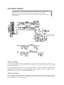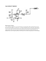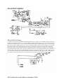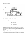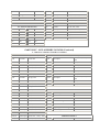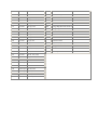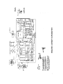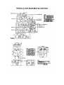
1
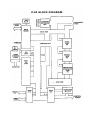
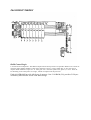
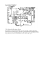
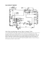
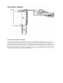
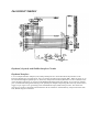
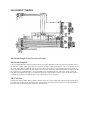
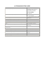
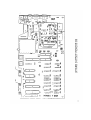
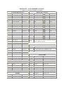
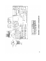
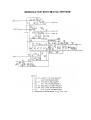
SERVICE MANUAL
MODEL C64 COMPUTER
SEPTEMBER 1985 PN-314001-02
Commodore Business Machines, Inc.
1200 Wilson Drive, West Chester, Pennsylvania 19380
U.S.A
Commodore makes no expressed or
implied warranties with regard to
the information contained herein.
The information is made available
solely on as is basis, and the entire
risk as to quality and accuracy is
within the user. Commodore shall
not be liable for any consequential
or incidental damages in connection
with the use of the information
contained herein. The listing of any
available replacement part herein
does not constitute in any case a
recommendation,
warranty
or
guaranty as to quality or suitability
of
such
replacement
part.
Reproduction or use without
expressed permission, of editorial or
pictorial content, in any matter is
prohibited.
This manual contains copyrighted and proprietary information. No
part of this publication may be reproduced, stored in a retrieval
system, or transmitted in any form by any means, electronic,
mechanical, photocopying, recording or otherwise, without the
prior written permission of Commodore Electronics Limited.
Copyright © 1985 by Commodore Electronics Limited.
All rights reserved.
Converted to PDF: [email protected] in Jan.2007
CONTENTS
•
SPECIFICATIONS
•
PRODUCT PARTS LIST
•
BLOCK DIAGRAM
•
CIRCUIT THEORY
o
POWER SUPPLY
o
RESET LOGIC
o
CLOCK CIRCUITS
o
I/O, RAM, EXPANSION LOGIC
o
RAM CONTROL LOGIC
o
5 PIN VIDEO AND AUDIO OUTPUTS
o
8 PIN VIDEO AND AUDIO OUTPUTS
o
CASSETTE INTERFACE
o
KEYBOARD, JOYSTICK & PADDLE INTERFACES
o
SERIAL INTERFACE, USER PORT
•
TROUBLESHOOTING GUIDE
•
BOARD IDENTIFICATION
•
PCB ASSEMBLY #326298-01
•
•
o
BOARD LAYOUT
o
PARTS LISTS
o
SCHEMATIC #326106
PCB ASSEMBLY #260407-04
o
BOARD LAYOUT
o
PARTS LIST
o
MODULATOR SCHEMATIC #251025
o
SCHEMATIC #251138
PCB ASSEMBLY #250425-01
o
BOARD LAYOUT
o
PARTS LIST
o
MODULATOR SCHEMATIC #251696
o
SCHEMATIC #251469
o
PIN ASSIGNMENTS
C64 COMPUTER
GENERAL DESCRIPTION
The "All Purpose" Commodore 64 us the complete computer for education,
home or small business applications. Supported by quality peripherals and a full
range of software, the Commodore 64 is perfect for the family. No other
computer can offer such variety of uses and applications at such an affordable
price.
MEMORY
64K RAM
ROM
20K ROM Standard (includes operating system and BASIC interpreter)
MICROPROCESSOR
6510A Microprocessor - 1.02 MHz clock
Compatible with the 6502
DISPLAY
40 Columns X 25 lines of text
COLORS
16 Background, border and character colors
CHARACTERS
Upper & lower case letters, numerals and symbols
Reverse characters
All PET graphic characters
DISPLAY MODES
Text characters
High resolution graphics
RESOLUTION
320 X 200 Pixels
SPRITES
8 independent sprites
Each consists of 24 X 21 pixels and up to 4 colors
Each independently expandable horizontally and vertically
Collision detection for sprite to sprite and data to sprite collisions
SOUND
6581 Sound Interface Device includes 3 independent tone generators - each
with 9 octaves
Each voice includes programmable ADSR generator (Attack, Decay, Sustain,
Release) and control of sawtooth, triangle, square, variable pulse and noise
waveforms
Full filtering capabilities with low, high and band pass filters
External sound input
KEYBOARD
Full size typewriter style design
KEYS
66 Keys total
2 Cursor control keys
4 Function keys (up to 8 user defined/programmable functions possible)
Upper and lower case character set
Graphic character set
INPUTS/OUTPUTS
User port
Serial port
ROM cartridge port
2 Joystick/paddle ports
Video port
C1530 Cassette drive interface port
FEATURES
Built-in BASIC 2.0 - over 70 commands, statements and functions
Full screen editor
PERIPHERALS
C1541 Disk drive
C1530 Datasette
MPS 801 Dot matrix printer
MPS 802 Dot matrix printer
MPS 803 Dot matrix printer
DPS 1101 Daisey wheel printer
C1520 Plotter/Printer
C1702 Color monitor
CM141 Color monitor
POWER REQUIREMENTS 120 Volts, 60 Hz
Specifications subject to change without notice.
PARTS LIST
C-64
PLEASE NOTE: Commodore part numbers are printed for reference only and do not indicate the availability of
parts from Commodore. Industry standard parts (Resistors, Capacitors, Connectors) should be secured locally.
Approved cross-references for TTL-chips, Transistors, etc. will be available in manual form through the Service
Department in November of 1984. Unique or non-standard part will be stocked by Commodore and are indicated
on the parts list by a "C".
TOP CASE ASSY
Top Case
Keyboard
LED Plate
Nameplate
Lamp Hold Set
LED Assembly
C 326113-01
C 326166-02
C 326160-01
C 326161-01
C 903820-03
C 1001039-01
BOTTOM CASE ASSY
Bottom Case
Foot, Self-Adhesive
PCB Shield Plate
PCB Insulation Sheet
C 326114-01
C 950157-04
C 326131-01
C 326288-01
ACCESSORIES
Users Manual
Power Supply
RF Cable
Switch Box
C 320974
C 251053-02
C 326189-01
C 904778-01
C64 CIRCUIT THEORY
There are three versions of the C64. The C64 with five pin connector video output
(326106). The C64 with an eight pin connector video output (251138), and the C64B
which has improved system clock circuit design (251469). Most circuit theory
explanations will be the same for all three versions. Refer to schematic 326106 unless
noted otherwise.
The Power Supply
The external power supply generates a regulated 5VDC and 9VAC. 5VDC is applied to pins 5 and 1 of CN7 on
the C64 pcb. Filtered by L5, C97, and C100 it is then controlled by on/off switch S1. This 5VDC output supplies
the microprocessor logic.
9VAC is applied to pins 6 and 7 of CN7 on the C64 pcb. +12VDC, +5VDC CAN and 9VAC
unregulated are outputs that are derived from this 9VAC supply. The 9VAC supply is made
available on pins 10 and 11 of the USER PORT CN2.
12VDC Generation
9VAC is added to 9VDC through CR6, and rectified by CR5. The unregulated DC output is filtered by C88 and
C89 then regulated at 12VDC by VR1. The regulated output is filtered by C57 and C59. The 12VDC supplies
the VIC and SID IC, and the audio amplifiers.
+5VDC CAN Generation
9VAC is rectified by CR4. The unregulated DC output is filtered by C19, and C95 then regulated at 5VDC by
VR2. The regulated output is filtered by C102 and C103. The output called 5VDC CAN is separated and
individually filtered into two outputs called Vvid and Vc. Vvid is the 5VDC supply for video circuits, and Vc is
the 5VDC supply for the clock circuits.
9VDC Unregulated Generation
CR4 rectifies the 9VAC input. The output is 9VDC unregulated. This supply powers the cassette motor transistor
amplifier circuits, and the RF modulator on the C64B version.
C64 CIRCUIT THEORY
Reset Logic Circuits
U20 is a 556 timer configured as a one shot multivibrator. The output pulse width is determined by the size of
R34 and C24. Pulse width = 1.1 x R34 x C24 = .5 seconds. The output on pin 9 is "high" active. The output of
U8 is "low" active. Reset initializes all the processor logic and causes the processor to load the program counter
register with the address of the first instruction of the operating system program called the KERNAL. The
starting address is stored in locations $FFFC and $FFFD. The first instruction is decode and executed giving
KERNAL control of the computer operations. The reset pulse occurs when turning the power on to the computer.
C64 CIRCUIT THEORY
The C64 Clock Circuits.
Crystal Y1 develops a 14.31818MHz fundamental frequency clock signal. U31 is a Dual Voltage Controlled
Oscillator. The output on pin 10 is a 14.31818 MHz clock signal called the color clock. R27 can be adjusted to
obtain exact output frequency. U30 is a frequency divider that outputs a 2MHz signal on pin 6. U29 is a D flip
flop which outputs a 1MHz signal on pin 9. U32 is a Phase/Frequency Detector which compares the output of
the U29 to the phase 0 clock, and outputs a dc voltage on pin 8 that is proportional to the phase difference
between the inputs. The second half of the Dual Voltage Controller Oscillator U31 generates an 8.1818MHz
clock signal called the DOT Clock. The VIC IC divides the DOT clock by eight and outputs this as the phase 0
clock on pin 17. The output of the Phase/Frequency Detector is applied to the frequency control input pin 2 of
U31. This causes tracking of the dot clock and the color clock because one input, pin 4 of U32, is the phase 0
clock which is derived from the dot clock, and the other pin 1 of U32, is derived from the color clock.
The C64B Clock Circuits. Refer to schematic 251469
Crystal Y1 develops the fundamental 16Mhz clock signal. U31 is a Clock Generator IC that outputs the
8.1818MHz DOT clock on pin 6, and the 14.31818 MHz color clock on pin 8.
C64 CIRCUIT THEORY
I/O and ROM Address Decoding and Expansion Port.
I/O Address Decoding Logic
U17 is a Programmable logic array (PLA). The output F5 on pin 12 called I/o goes "low" when any of the I/O
devices controlled by U15 are selected. The addresses are listed below for each device.
VIC IC
$D000 - $D02E
SID IC
$D400 - $D7FF
Color Ram $D800 - $DBFF
CIA 1
$DC00 - $DC0F
CIA 2
$DD00 - $DD0F
I/O 1
$DE00 - $DEFF
I/O 2
$DF00 - $DFFF
ROM Address Decoding.
Basic ROM resides at locations $A000 - $BFFF. The output F1 pin 17 of the PLA U17 goes "low" when the
BASIC ROM is selected. The KERNAL ROM resides at locations $E000 - $FFFF. The output F2 pin 16 of the
PLA U17 goes "low" when the KERNAL ROM is selected. The CHARACTER GENERATOR ROM resides at
locations $D000 - $DFFF. The output F3 pin 15 of the PLA U17 goes "low" when the Character Generator
ROM is selected.
The Expansion Port Connections.
The expansion port is an extension of the microprocessor address, data, and control bus. ROML decodes
addresses $8000 - $9FFF, and ROMH decodes addresses $E000 - $FFFF. These are outputs from the PLA used
to select the catridge inserted in the expansion port. I/O 1 input from U15 decodes addresses $DE00 - $DEFF.
I/O 2 output from U15 decodes addresses $DF00 - $DFFF.
C64 CIRCUIT THEORY
RAM Control Logic.
U13 and U25 are multiplexers. The address output from the microprocessor are passed to RAM via U13 and U25
when the output Address Enable Control (AEC) from the VIC IC is "high". When AEC is "low" the VIC IC
outputs refresh addresses on pins 24 - 31. AEC goes "low" when the system clock, phase 2, is "low". Since all
I/O decoding occurs when phase 2 is "high", refresh is transparent to the processor.
Eight 4164 DRAMS provide 64k bytes of memory. One 2114 RAM (U6) provides 512 bytes
of memory allocated for screen color data storage.
C64 CIRCUIT THEORY
5 Pin Video and Audio Output Circuits
Pin 15 of the VIC IC is the sync/luminance output. Pin 14 is the color output. A composite video output is
created by mixing sync/luminance and color. The composite output is applied to the RF modulator, and also
passed to the monitor connector CN5 on pin 4. The color output is not made available on the monitor connector
CN5 as on the 8 pin version, and the RF modulator mixes audio with the composite video producing the TV RF
output, unlike the 8 pin version RF modulator which creates the composite video output.
C64 CIRCUIT THEORY
8 Pin Video and Audio Output Circuits. Refer to schematic 21469
U19 is the Video Interface Chip (VIC). Sync (horizontal and vertical), and luminance (video) is output on pin 15.
This signal is passed to pin 2 of the RF modulator. Color is output on pin 14, and passed to pin 3 of the
modulator. Light pen inputs are sensed by the VIC IC on pin 9. U18 is the Sound Interface Device (SID). The
audio output is on pin 27, and audio input is on pin 26. The RF modulator mixes sync/luminance, color, and
audio out, generating a TV composite signal on pin 5. The RF modulator also passes the VIC outputs to the
monitor connector CN5. Audio out on pin 27 is amplified by Q2, and output on pin 3 of CN5. Audio in is
applied to pin 5 of CN5, then to pin 26 of the SID IC. Inputs from paddles connected to on of the control ports
are monitored by the SID IC on pins 23 and 24.
C64 CIRCUIT THEORY
The Cassette Interface Circuits.
U7 is a 6510 microprocessor. One of the features of the 6510 is a built in parallel I/O port (P0-P5). P3 - P5
control most of the cassette interface circuitry. P3 pin p6 of U7 outputs the write data signal to connector CN3 on
pins E and 5. P4 is an input that senses the play switch depressed on the cassette deck. P5 is on output that
controls the cassette motor. When P5 goes "low", Q2 cuts off, CR2 regulates Vb of Q1 at 7.5 volts, this forward
biases Q1 and Q3, passing current through the cassette motor coil. U1 is a Complex Interface Adapter (CIA).
Parallel ports, serial outputs, and Timers are standard features of the CIA. Read data enters on pins D, 4 of CN3.
U1 accepts the read data signal on the FLAG input pin 24.
C64 CIRCUIT THEORY
Keyboard, Joystick, and Paddle Interface Circuits.
Keyboard Interface
U1 is a Complex Interface Adapter (CIA). Both parallel ports are used to decode the keyswitches on the
keyboard. Parallel port A signals (PA0 - PA7) are outputs. PArallel port B signals (PB0 - PB7) are inputs. A "0"
bin is shifted through the parallel port A, when a key is depressed on the keyboard the "0" bit is returned on one
of the parallel port B inputs. A program in the KERNAL ROM generates the shifting "0" bit output on parallel
port A, and decodes the signals returning on the parallel port B inputs. Depressing the restore key causes U20 to
trigger. U9 pin 6 goes "low" generating a Non- Maskable Interrupt (NMI) at the processor. This causes the
processor to execute a subroutine which initializes the I/O interfaces. If the STOP key is depressed at the same
time, BASIC flags are initialized.
Joystick Interface
U1 also controls the joystick. Parallel port A accepts inputs from the B joystick connected to control port 2.
Parallel port B accepts inputs from the A joystick connected to control port 1. When the joystick is moved up,
down, left, right, or the fire button is depressed, a ground potential is applied to the appropriate input of U1.
Paddle Interface
A Variable resistor is connected to adjusting knob on the paddle. When the knob is rotated, the resistance varies
controlling the time constant of an RC network. The Voltage developed across the capacitor is input to an A/D
converter internal to the SID chip U18. The digital output is stored in one of the SID registers. The paddle
position can be determined by the reading the contents of the appropriate register. U28 is a 4066 CMOS switch.
The signals from the paddles are passed to the SID chip when the Enable inputs (E0 - E3) of U28 are "high".
NOTE: U1 port assignments are incorrect on
schematics. Refer to Keyboard Matrix for
correct assignments.
C64 CIRCUIT THEORY
The Serial Interface and User Port Circuits
The Serial Interface.
U2 is a Complex Interface Adapter (CIA). Parallel port signals PA3-PA7 control the serial bus interface. PA3 is
the Attention (ATN) output. This signal is inverted by U8 before being transmitted to a device on the bus. PA4 is
the clock output. Data transmitted from the C64 to a device on the bus is synchronized by this clock signal. U8
inverts the output PA4. PA5 is the data output. U8 inverts this output also. Data transmitted from a device on the
bus to the C64 is synchronized by a clock generated by the transmitting device. The Clock signal is input on
PA6. Data transmitted from a device on the bus to the C64 is input on PA7. When a device on the bus wants to
communicate with the C64, SQR IN goes "low" indicating service is requested.
The User Port
Parallel port B of U2 (PB0 - PB7) is made available on the user port. Parallel data transfers with external device
are made very easily through this parallel port. SP2 and SP1 are bi-directional serial ports. CNT1 and CNT2 are
bi-directional synchronizing clock signals for each serial bus.
64 TROUBLESHOOTING GUIDE
SYMPTOM
POSSIBLE SOLUTION
Blank screen on power up.
Check External Power Supply
U4 (KERNAL ROM), U17 (PLA)
U7 (6510 MPU), U3 (ROM)
U8 (7406 IC), U19 (VIC II)
U9-U12 (4164 RAM)
U21-U24 (4164 RAM)
BT2, CR4, VR1
Out of memory error on power up.
Check U9-U12 (4164 RAM)
U21-U24 (4164 RAM)
**** USE DIAGNOSTIC TEST - DISK
No cursor displayed. Intermittent blank screen.
Check U1, U15, U7
Check U2, U7
Powers up with graphics display and blinking cursor
Check U14 (74LS258 IC)
Powers up with all the characters displayed as blocks.
Check U26 (74LS373 IC)
Intermittent display.
Check C88 (Possible Bad Connection)
Powers up with the 'PRESS PLAY ON TAPE' message and the display Check U7 (6510 MPU)
blanks
R1 (Possible Bad Connection)
On power up the cursor lock up.
Check U7 (6510 MPU)
U20 (556 IC)
When 'RETURN' is pressed after a run command, the cursor goes back Check U3 (ROM)
to home position.
Poke command does not work.
Check U3 (ROM)
Joystick does not operate correctly.
Check U1, U28 (6526 CIA)
Wrong frequency.
Check C70
No character lettering is displayed on the screen.
Check U3 (ROM)
U2 (CIA)
Graphic characters instead of letters displayed.
Check U19 (VIC II)
Power up message appears but no cursor.
Check U1, U15, U7 and U4
SYMPTOM
POSSIBLE SOLUTION
Cursor jumps to back to home position.
Check U7 (6510 MPU)
Abnormal colors appear in the letters.
Check U6 (2114 RAM)
U16 (4066 IC)
Different characters are displayed and cursor is locked when turned on and off.
Check RAM
System does not reset and the 'RESTORE' key does not work.
Check U20 (556 IC)
White band scrolls down the screen. (60 HZ HUM)
Check External Power Supply
VR2 (5V Regulator)
Cursor disappears after the system warms up.
Check U1 (6526 CIA)
SYNTAX ERROR displayed after system warms up.
Check RAM, U3 (ROM)
Wavy screen after the system warms up.
Check External power supply
U31 (74LS629 IC)
U30 (74LS193 IC)
The system resets when it warms up.
Check U7 (6510 MPU)
U3 (ROM)
Keyboard does not operate correctly when the system warms up.
Check U1 (6526 CIA)
U3 (ROM)
Black band scrolls through screen when the system warms up.
Check External Power Supply
C90, C88, CR4
VR2 (5V Regulator)
Cassette motor keeps running.
Check U7 (6510 MPU)
Cassette motor keeps running even after a program is done loading. The TIP 29
transistor gets extremely hot and the fuse may possibly blow.
Check Cassette Port for Shorts
R4 (Possibly Open)
The cursor disappears when the cassette is plugged in.
Check U7 (6510 MPU)
Cassette runs extremely slow. The program seems to load but will not run.
Check U7 (6510 MPU)
SYMPTOM
POSSIBLE SOLUTION
When loading from cassette, the 'SYNTAX ERROR' message is displayed.
Check U20 (556 IC)
DEVICE NOT PRESENT ERROR is displayed when disk is used.
Check U1 (6526 CIA)
U7 (6510 MPU)
R28, R29, R30
Disk drives continue to search when trying to load.
Check U2 (6526 CIA)
When loading from disk and any key of the 4th row of the keyboard is pressed,
the cursor goes to home position.
Check U20 (556 IC)
R35 (Possible Bad Connection)
When loading from disk, a 'FILE NOT FOUND' message is displayed.
Check U4 (ROM)
U2 (6526 CIA)
OUT OF MEMORY is displayed when disk is used.
Check U20 (556 IC)
C64 BOARD IDENTIFICATION
To date there are 4 version of 64 PCB assemblies in use.
VERSION
IDENTIFYING FACTORS
PCB ASSY #
SCHEMATIC #
Original
5 pin board
(CN5-Video port has 5 pins)
326298-01
326106
A (CR)
8 pin board
(CN5-Video port has 5 pins)
250407-04
251138
B
8 pin board
(Reduced oscillator circuit)
250425
251469
B-2
8 pin board
250441-01*
251469
These boards are interchangeable with casework, keyboard, etc.; however, care must be taken
to provide the customer with a unit that is compatible with their monitor and cable.
When component level repairs are necessary, be certain to acquire the appropriate part for the
board you are repairing. Most modulators are different, as are many of the components.
* The 4th version of 64 board was recently developed and only a few may be in the field. It is
termed the 64B-2. All circuits remain the same as the 64B (Schematic 251469) with a few
component location changes:
1) Resistors 28, 29, 30, 36, 48 were reduced to Resistor Pack RP5.
2) Diodes CR100-105 are no longer piggybacked. Their new locations are CR9, 12-16.
PARTS LIST - PCB ASSEMBLY #326298
C - Indicates Commodore Stocked Part Numbers
RESISTORS (continued)
INTEGRATED CIRCUITS
U1,U2
6526 CIA
C 906108-01
R14
100
R30
1K
U3
2364 Basic ROM
C 901226-01
R16
1K
R31
180
U4
2364 Kernal ROM
C 901227-03
R17
1.2K
R33
47K
U5
2364 Char ROM
C 901225-01
R19
15K
R34
47K
U6
2114L-30 RAM
901453-01
R20
6.8K
R35
470K
U7
6510 uProcessor
C 906107-01
R21
4.7K
R37
2.7K
U8
7406
901522-06
R22
1.5K
R38
1K
U9-U12
4164 (200 nS)
901505-01
R23
1K
R39
390
U13
74LS257
901521-57
R24
3.3K
R41
1M
U14
74LS258
901521-58
R25
Pot 1K
R43
3.3K
U15
74LS139
901521-18
R26
75
R44
3.3K
U16
4066
901502-01
R27
Pot 2K
R45
3.3K
U17
82S100 PLA
C 906114-01
R28
1K
R46
2K
U18
6581 SID
C 906112-01
R29
1K
R51
1.5K
U19
6567 VIC II
C 906109-04
NOTE:
U20
LM556
901523-03
The input video line requires a 470 ohm, 1/4 watt,
resistor soldered to ground.
U21-U24 4161 (200 nS)
901505-01
U25
74LS257
901521-57
U26
74LS373
901521-29
RP1,2
33, 8 Pin (Bourne No. 430BR-102-330)
U27
74LS08
901521-03
RP3
33K, 8 Pin (Bourne No. 430BR-101-332)
U28
4066
901502-01
RP4
3.3K, 10 Pin
U29
74LS74
901521-06
U30
74LS193
901521-26
U31
74LS629
901521-68
C1-3
Ceramic
.1 uF, 50V
U32
MC4044
906128-01
C4-7
Ceramic
.47 uF, 50V, 20%
C8
Electrolytic
10 uF, 25V, +50%, -10%
C9
Ceramic
.47 uF, 50V, 20%
TRANSISTORS
RESISTOR PACKS
CAPACITORS
Q1
2N4401
902652-01
C10-11
Ceramic
470 pF, 50V
Q2
2N3904
902658-01
C12-15
Electrolytic
10 uF, 25V, +50%, -10%
Q3
TIP29 B
902653-01
C16
Ceramic
.1 uF, 50V
Q4-8
2N2222
902686-01
C17
Electrolytic
10 uF, 25V, +50%, -10%
C18
Ceramic
.1 uF, 50V
C19
Electrolytic
2200 uF, 16V
DIODES
CR1
2.7V Zener IN4371
C20,21
Film
.22 uF, 100V, 20%
CR2
7.5V Zener IN755
C22
Ceramic
.1 uF, 50V
CR3
IN914
C23
Ceramic
360 pF, 50V
CR4
Bridge, Varo VMO8 906129-01
C24
Electrolytic
10 uF, 25V, +50%, -10%
CR5,6
Rectifier IN4001
C25-28
Ceramic
.22 uF, 50V
C29
Ceramic
.47 uF, 50V, 20%
RESISTORS - All values are in ohms- 1/4W,
5%, unless noted otherwise.
C30,31,32 Ceramic
.1 uF, 50V
C33
Ceramic
.47 uF, 50V, 20%
R1
3.3K
R7
10K
C34
Electrolytic
10 uF, 25V, +50%, -10%
R2
1.5K
R8
390
C35
Ceramic
.1 uF, 50V
R3
10K
R9
75
C36
Ceramic
20 pF, 50V
R4
1K
R10
120
C37
Ceramic
1000 pF, 50V
R5
560
R11
120
R6
1K
R13
1K
PARTS LIST - PCB ASSEMBLY #326298 (Continued)
C - Indicates Commodore Stocked Part Numbers
CAPACITORS (Continued)
CAPACITORS (Continued)
10 uF, 25V, +50%, 10%
C38
Ceramic
51 uF, 50V
C94
Electrolytic
C39
Ceramic
.1 uF, 50V
C95,96 Ceramic
.1 uF, 50V
C40-43
Ceramic
.22 uF, 25V, +50%, -10%
C97
.22 uF, 25V
C44
Ceramic
.47 uF, 50V, 20%
C98,99 Ceramic
.1 uF, 50V
C45,46,47 Ceramic
.1 uF, 50V
C100
Ceramic
.22 uF, 25V
C48
Ceramic
1800 uF, 50V
C101
Ceramic
.1 uF, 50V
C49
Ceramic
470 pF, 50V
C102
Electrolytic
10 uF, 25V, +50%, 10%
C50
Ceramic
.22 uF, 50V
C103
Ceramic
.1 uF, 50V
C51
Ceramic
.47 uF, 50V, 20%
C105
Ceramic
.1 uF, 50V
C52,53
Ceramic
470 pF, 50V
C54
Ceramic
.22 uF, 50V
C55
Ceramic
.1 uF, 50V
CN1
Header Assy 20 Pin
903331-20
C56
Ceramic
.1 uF, 50V
CN4
6 Pin Din
C 903361-01
C57
Electrolytic 10 uF, 25V, +50%, -10%
CN5
5 Pin Din
C 903362-01
C58
Ceramic
.1 uF, 50V
CN6
44 Pin Card Edge
C 906100-02
C59
Ceramic
.22 uF, 50V
CN7
7 Pin Din
C 906130-01
C60,61
Ceramic
.47 uF, 50V, 20%
CN8,9 Plug Assy, 8 Pin Rt. Angle
C62
Electrolytic 10 uF, 25V, +50%, -10%
C63
Ceramic
C64,65
Electrolytic 10 uF, 25V, +50%, -10%
C66,67
Ceramic
Ceramic
CONNECTORS
CN10
C 906126-01
Header Assy, 3 Pin
.47 uF, 50V, 20%
.47 uF, 50V, 20%
MISCELLANEOUS
L1,2
Coil Inductor 2.2 uH
901151-17
C68
Ceramic
.1 uF, 50V
C69
L3
Coil Inductor 3.0 uH
901151-21
L4
Filter Line Assy
C 906127-01
C70
Mica
10 pF, 500V, 5%
L5
Coil Inductor 1.2 uH
901152-01
C71
Ceramic
.1 uF, 50V
Y1
Crystal 14.31818 MHz
C 900558-01
C72
Ceramic
220 pF, 50V
SW1
Rocker Switch DPDT
C 904500-01
C73
Ceramic
150 pF, 50V
VR1
Voltage Regulator MC7812CT
C74
Ceramic
.1 uF, 50V
VR2
Voltage Regulator MC7805CT
C77
Ceramic
.1 uF, 50V
M1
Modulator
C78
Ceramic
220 pF, 50V
F1
Fuse, Normal Blo, 250V, 1.5A
C79
Ceramic
510 pF, 50V
FB1-23 Ferrite Bread
C80
Ceramic
51 pF, 50V
Connector Panel
C81
Ceramic
20 pF, 50V
(ON, OFF, Joystick)
326299-01
C82
Ceramic
.1 uF, 50V
Catridge Guide
326116-01
C83
Mica
.33 pF, 500V, 5%
Shield Box
C 326265-01
C84
Ceramic
.1 uF, 50V
Shield Cap
C 326267-01
C85
Ceramic
.47 uF, 50V, 20%
C86
Mica
39 pF, 500V, 5%
C87
Ceramic
.1 uF, 50V
C88
Electrolytic 470 uF, 50V
C89
Ceramic
C90
Electrolytic 470 uF, 50V
C91
Electrolytic 100 uF, 16V
C92
Ceramic
.22 uF, 50V
C93
Ceramic
1800 uF, 50V
.1 uF, 50V
C 326130-01
903025-01