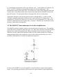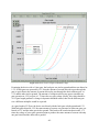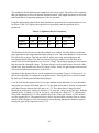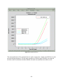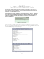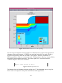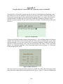
1
Optimization of Device Performance Using Semiconductor TCAD Tools Thursday, May 3, 2001 Advisor: Ashok K. Goel Team Members: Matthew Merry Kathryn Arkenberg Eric Therkildsen Emanuel Chiaburu William Standfest Table of Contents 1 Introduction 1.1 Project Overview 1.2 Objectives 1.3 Project Definition 1.3.1 Understand the Devices 1.3.2 Learn the Usage of the Software Package 1.3.3 Simulate and Optimize Devices 1.4 Project Management 1.5 Paper Structure Overview 1 1 1 1 1 3 4 5 5 2 MOSFET 2.1 Introduction and History of MOSFETS 2.2 Enhancement Versus Depletion type MOSFETS 2.3 Structure and Physical Operation of Enhancement type MOSFETS 2.4 Current-Voltage Characteristics of Enhancement type MOSFETS 2.5 The MOSFET Transconductance involved with amplification 2.6 Basic Fabrication Process 2.7 MOSFET Fabrication Procedures Implemented with ATHENA 2.8 Device Amplification 2.9 MOSFET Optimization 7 8 11 15 19 21 24 27 30 3 Silicon-On-Insulator MOSFET Design 3.1 What is am SOI Device 3.2 Design Approach 3.3 Original SOI Device Design 3.4 Optimized SOI Device Design 38 38 40 41 42 4 Dual Gate Volume Inversion SOI MOSFETS 4.1 Introduction to Dual Gate Volume Inversion SOI MOSFETS 4.2 Design Approach 4.3 Original Design 4.4 Optimization 48 48 50 51 52 5 Conclusions and Recommendations for Further Research 66 Appendix A MOSFET 68 Appendix B SOI 96 Appendix C Dual Gate SOI 110 1.0 Introduction 1.1 Project Overviews The purpose of this project was the optimization of device performance using Semiconductor TCAD tools. Semiconductor TCAD (Semiconductor Technology Computer Aided Design) tools are computer programs which allow for the creation, fabrication, and simulation of semiconductor devices. These tools were used to optimize semiconductor devices for various applications. During the course of this project, these programs were used to create simulations of the devices being worked on. These simulations provided the opportunity to study the effect of different device parameters on the overall device performance. Throughout the year, the devices were simulated and gradually the performance of each one was improved, until an optimal device configuration was created for the particular applications. 1.2 Objectives The overall objective of this project was the optimization of the various semiconductor devices. In order to achieve this goal, several intermediate objectives were needed. • • • • • • • • Understand each device and the applications for which it is used Learn and understand the use of Silvaco's TCAD software Create an initial device design using reference material from Silvaco's web-site Generate benchmarks for initial device design Choose an application for which the device is to be optimized Vary device parameters and study resulting effects upon performance Determine optimal values for each device parameter Combine the optimal parameters into a final, fully optimized device The accomplishment of each of these intermediate objectives was critical to the success of the project as a whole. All these objectives can be grouped under three main categories and are expanded upon in the following section. 1.3 Project Definition 1.3.1 Understand the Devices First and foremost a basic understanding of the fabrication, operation, advantages, and applications of each device was needed before any simulations or optimizations could commence. This understanding of the devices was gained through extensive research conducted on each device. Various sources were consulted and the resultant understanding of the devices was key in the creation of optimized device configurations. -1- Three devices were selected for optimization during the course of this project. These devices are the MOSFET (Metal-Oxide-Semiconductor Field Effect Transistor) device, the SOI (Silicon-OnInsulator) device, and the VI-MOSFET (Volume Inversion – MOSFET). An in-depth report on the research conducted can be found under each individual device section. For the purposes of the introduction, a general device overview is given. MOSFET technology is an industry standard. This technology has been around for many years, and the fabrication methods are continually improving, yet they are well established. There has been a consistent gain in the performance of these devices every few years since their creation. The cost and size are main advantages of MOSFET devices. Since the technology is well established, fabrication methods have become relatively inexpensive. Also, the device itself is physically smaller than other technologies, allowing for the placement of more devices on a silicon wafer during fabrication. MOSFET devices are mainly used in the creation of CMOS logic chips, which are at the heart of every computer. An enhancement-type NMOS transistor was used during the course of this project. Figure 1-1 shows the basic structure of this style MOSFET device. SOI (Silicon-On-Insulator) devices are a relatively new technology. Although the technology has Figure 1-1 Physical structure of an enhancement-type NMOS transistor been around since the 1960’s, SOI devices are only recently becoming commercially viable, due to the expense associated in producing the devices.[1] SOI devices are an advancement of standard MOSFET technology. The main difference between SOI and MOSFET technology is the inclusion of a insulating layer. SOI devices are created from a thin layer of silicon placed on top of a layer of insulating -2- material. This structure can be seen in figure 1-2. Most often this material is silicon oxide, however other insulating materials are being tested, such as diamond, sapphire, and ruby.[2] For this project, a buried oxide layer (BOX) of silicon dioxide was used for the creation and simulation of the SOI device. The third technology for which optimization was pursued is the VI-MOSFET (Volume Inversion MOSFET) device. This device takes advantage of the buried oxide layer of a SOI device by adding a second gate beneath the device’s channel. This allows for greater control of the device switching, and opens the doors for great advances in device design. The VI-MOSFET is by far Figure 1-2 Physical structure of basic SOI device the newest, and most advanced semiconductor technology simulated during the course of this project, further explanation of this device and the others simulated during the project, can be found under the individual device sections. 1.3.2 Learn the Usage of the Software Package Once a basic understanding of each device was acquired, and in some cases while research on the device was proceeding, the operation of the software package needed to be learned. The software package used for this project is Virtual Wafer Fab (VWF) package created by Silvaco International. VWF is a suite of software programs used to create a multi-functional environment for the simulation of semiconductor technology. Several different programs were learned and then used throughout the year, allowing for simulation of these devices on many different levels. After trying different programs in the suite, simulation efforts were focused on using ATHENA, ATLAS, DevEdit, and DeckBuild. [3] -3- ATHENA is a framework program that integrates several smaller programs into a more complete process simulation tool. It is a modular program that combines one and two-dimensional simulations into a more complete package allowing for the simulation of a wide range of semiconductor fabrication processes. This program’s focus is upon the simulation of fabrication processes. In ATHENA, devices are created through simulation of the fabrication process. [4] ATLAS is a device simulation tool. The framework of ATLAS combines several one, two, and three-dimensional simulation tools into one comprehensive device simulation package. This allows for the simulation of a wide variety of modern semiconductor technologies. Devices can be created in ATLAS through layout based simulation syntax, however the main focus of this program is simulation of the device once fabrication is complete. [4] DevEdit is a program that allows for structure editing, structure specification, and simulation grid generation. All of Silvaco’s programs use a mesh or grid to determine the level of detail that the simulation will generate in a specific area of the device, allowing users to cut down on simulation time by removing detail from areas with uniform or no reaction to performance simulations. The creation of these meshes is the main function of DevEdit, however it is also be used for the editing and specification of two and three-dimensional devices created with the VWF tools. [5] DeckBuild is the front-end GUI (Graphical User Interface) for Silvaco’s Virtual Wafer Fab programs. This program is the framework which ties together the wide range of process and device simulation tools available, and allows them to work together seamlessly and efficiently. DeckBuild uses pull-down menus to generate syntax for the various programs, and provides basic simulation controls such as stop, pause, and restart. The use of ATHENA, ATLAS, and DevEdit are expanded upon in later sections of this report, DeckBuild was used for front-end simulation control in each case. [5] In order to learn the usage of these programs, many sources were consulted. Various device examples are available through the Silvaco’s homepage. Through the usage of these examples and research material available through the company’s web-site and user manuals, a basic knowledge of each program’s operation was gained. Once this operational level of understanding was acquired, research into the effects of device parameters upon performance could begin. 1.3.3 Simulate and Optimize Devices Once an understanding of the device and the software was obtained, the simulation and optimization of the devices could begin. The first step in optimization is the selection of an initial device configuration. Using reference material and example programs available through Silvaco’s homepage, initial device designs were created, taking into account the time limitations of this project. These initial configurations were designed to be simple, yet straightforward examples each device’s capabilities. -4- Once initial devices were selected, a goal for optimization was needed. It was decided that the devices would be optimized for low power, high-speed applications. In order to determine the optimal configuration, the ID vs. VGS curves were examined. A lowered threshold voltage and an increased transconductance became the optimization goals of the project. Improving these two parameters would produce a lowered operating voltage, and increased switching speed. Optimization for radiation hardness, and three-dimensional “device stacking” were two other objectives considered for the project. However, after further research both these goals were determined to be beyond the scope of this project, and were ultimately removed from the list of design goals. Optimization of these devices using the TCAD tools requires many hours of lab simulation time. Several aspects of each device were selected for optimization. Once the device characteristics were selected for optimization, the process of device simulation began. First each parameter was tested individually for its effect on device performance as a whole. Once several plots were obtained that indicated the particular parameter’s effect on device performance, improved values could then be selected for the device. Several simulations needed to be run to find improved values for each device parameter, until an optimal value was reached. Once an optimal value was reached for each of the device parameters, the improved parameters were then recombined into a single device. Once these new values were all present in a single device, they were again simulated and adjusted to optimize based upon their combined effects, to ultimately produce an optimal device configuration. 1.4 Project Management This project was divided into two groups for the initial optimizations of the SOI device, and the MOSFET device. Matthew Merry, Kathryn Arkenberg, and William Standfest worked for optimization of the SOI device. Emanuel Chiaburu and Eric Therkildsen optimized the MOSFET device. When the VI-MOSFET was added to the list of devices, Matthew Merry, and Eric Therkildsen were the group members focusing on optimizing this device. 1.5 Paper Structure Overview The remainder of this paper focuses on each aspect of this project in far more detail. Explanations are given of each program used for simulation, the design methods used, reasons for the choosing of each device, detailed information about the function of each device, and step by step explanations of the steps taken during optimization. The appendices of this report contain detailed information regarding the usage of each program, explaining syntax, input procedures, plotting methods, and techniques for optimization of the devices. The MOSFET is the first device discussed in this paper due to the relative simplicity of the device. Once a basic understanding of the MOSFET and the optimization approach for this device is grasped, the SOI and VI-MOSFET devices become easier to understand. The SOI device is explained second in this paper, because of ts many similarities with MOSFET technology. The SOI concepts are used as a foundation for understanding VI-MOSFET devices. -5- -6- 2 MOSFET 2.1 Introduction and history of MOSFETs The MOSFET is the earliest and most basic device out of the three devices reviewed in this document. The operation and physical structure is the basic starting point for the development of the SOI and Dual-gate SOI device. A FET (Field-Effect-Transistor), in principle, operates on the electric fields effect on the channel of the transistor which gives rise to its name. A MOSFET is just one type of FET available in today's market but it is definitely the most common for a variety of reasons. The basic operation and structure is conveniently found in the name of this device, MOSFET (Metal-OxideSemiconductor Field-Effect-Transistor). The ending, FET, relays that this device is governed by electric field control of a channel and MOS (Metal-Oxide-Semiconductor) shows the basic physical device materials. The metal is used for contact electrodes and interconnections, the oxide is present for barriers and isolation and the semiconductor substrate with a specified doping profile provides the necessary physics for developing the characteristics. A MOSFET may also be referred to as a unipolar device due to the nature of its design. Specifically, the majority carriers in the channel region can be of only one type (electrons or holes) [2-2]. The MOSFET with electrons as the majority carriers in the channel is entitled an n-channel MOSFET or NMOS. Similarly, the MOSFET with holes as the majority carriers in the channel is a p-channel MOSFET or PMOS. There are many reasons why the MOSFET has been the most popular device for a vast array of applications. Since the 1970s the MOSFET has been the prevailing device in microprocessors, memory circuits and logic applications of many kinds [2-2]. The fabrication process for MOSFET has become very mature over the 25 to 30 year lifetime of this device [9]. These mature fabrication processes leads to less errors and discrepancies in circuit construction and gives rise to a higher yield of good devices. This technology is now well-developed and similar processes of MOSFET fabrication are widely used in industry throughout the world. Size cost reduction has followed the MOSFET through its history. In the initial stages of the MOSFETs development a 10-micron gate length was a standard design goal [9]. This length would prove to decrease significantly as time past with engineers striving to increase speed and component count per unit area. The gate length (the natural measure of the device technology) has been reduced by a factor 2 about every 5 years [9]. First, large-scale integration (LSI) could fit hundreds of components onto a single chip and by the 1980's, very large-scale integration (VLSI) became the prominent technology allowing hundreds of thousands of components to exist on one chip [11]. Ultra large-scale integration (ULSI) followed quickly behind yielding millions of components per chip the size of a dime [11]. It also increased their power, efficiency and reliability. The very useful and natural insulator of silicon, silicon dioxide (SiO2), plays an important part in this size reduction due to its superb ability to provide insulation between -7- components. Many other semiconductor materials do not have such a useful native insulating material such as this. Today, .25 micron technology is manufactured on a large scale [10]. Wafer sizes are also increasing periodically and 8-inch wafer technology is now becoming common in industry. As a result, semiconductor circuit production volume has increased tremendously. By the year 2010, .1 micron and sub-.1 micron gate length MOSFET technology is expected to become mainstream [10]. Although this gate length has already been fabricated in a laboratory setting, the scaling of other aspects have not yet been accomplished. This booming industrial field seems to comprise unlimited potential while the demand for the smaller and faster device remains. The cost of these circuits produced naturally came down as the technology developed. Less material used is a big factor in this reduction. The functions performed on several chip and other components can now be performed quicker and with less power dissipation on a much smaller chip. Reduced total manufacturing time also plays a role as the mature fabrication processes are implemented with high-speed and greater volume machines. Price reduction can also be attributed to an increased yield of circuits per silicon wafer resulting from procedures that are cleaner, reproducible and reliable [9]. Another great advantage the MOSFET brought was CMOS (Complementary-Metal-OxideSemiconductor) technology. Initially PMOS logic families were exclusively employed because of its high-yield manufacturing processes. Later, as manufacturing condition improved (specifically, airborne particulate and impurity contamination was reduced), NMOS logic circuits became the norm because of their improved performance compared to PMOS technology. More recently, CMOS technology, which employs both PMOS and NMOS transistors, has become very prominent because of its ability to dramatically reduce power dissipation. Essentially, CMOS operates on state switching instead of the common voltage drop model lowering current flow and power loss. This technology can be used to single handedly simulate many different functions. 2.2 Enhancement Versus Depletion Type MOSFETs There are four main types of MOSFETs available that differ in construction and operation. The n-channel enhancement type MOSFET, the p-channel enhancement type MOSFET, the n-channel depletion type MOSFET and the p-channel depletion type MOSFET compose this set of transistors. The difference between the n-channel and the p-channel device was outlined previously by stating that the FET channels contain majority carriers that are composed of electrons and holes, respectively. Note that in an n-channel MOSFET, inverting the substrate surface from p-type to n-type creates the channel. Hence the induced channel is also called an inversion layer. With a small value of vDS applied it is possible to examine the effect of an increase in gate voltage. After reaching the threshold voltage (Vt) the induced n channel begins to increase in -8- depth (effectively decreasing the resistance). In fact, the resistance is inversely proportional to the value vGS-Vt (excess gate voltage or effective voltage). Therefore, the current iD is almost linearly proportional to this effective voltage. The name "enhancement-type" is tacked onto this type of MOSFET as a result of the gate voltage having to overcome the threshold voltage and enhance the channel [2-2]. Figure 2-1 shows the iD vs. vGS characteristics for this enhancement-type NMOS transistor in saturation. Figure 2-1: The iD - vGS characteristic for an enhancement-type NMOS transistor in saturation (Vt = 1 V and k'n(W/L) = 0.5 mA/V2). A depletion-type MOSFET has about the same theory of operation as the enhancement-type except that the depletion-type has a physically implanted channel. Any voltage (vDS) applied will create a current for vGS = 0. There is no need to invert the substrate type in order to create a channel, unlike the case of the enhancement MOSFET. The majority carriers needed for current flow are already present in this type of MOSFET. A negative vGS can be applied to deplete the channels charge carriers and increase effective resistance. This mode of operation is called the depletion mode [2-2]. The threshold voltage of this operation happens when current reaches zero. Alternatively a positive vGS can be applied to operate in the enhancement mode. See Figure 2-2 for a detailed plot of these characteristics when vDS $ vGS-Vt. -9- Figure 2-2: The iD - vGS characteristic in saturation . Because Vt is negative, the depletion NMOS transistor will operate in the triode region as long as the drain voltage does not exceed the gate voltage by more that |Vt|. For it to operate in saturation, the drain voltage must be greater than the gate voltage by at least |Vt| [2-2]. Figure 2-3: The iD- vGS characteristics of MOSFETs of enhancement and depletion types, of both polarities (operating in saturation). The p-channel depletion-type MOSFETs operate in the same manner as the n-channel depletion-type MOSFETs described above with some polarities reversed including Vt. Figure -10- 2-3 is a great summary of the basic difference between the enhancement and depletion types (operating in saturation) in graphical form. 2.3 Structure and Physical Operation of the Enhancement-Type MOSFET This section will explain the very generalized physical structure and operation of the most widely used FETs, the enhancement-type MOSFET. This information will provide us with the necessary base to show the specific characteristics of this device. Eventually, a more complex fabrication procedure and theory of operation will be described in this document. The NMOS transistor is fabricated on a p-type substrate or p-well, which is the starting point for fabrication of every component with this common construction. Two heavily doped n-type regions are then symmetrically created on this substrate, the n+ source and n+ drain (n+ denotes heavily doped n-type silicon). The gate electrode is then constructed by allowing silicon dioxide (SiO2) to form about 0.02 to 0.1 microns on the surface and placing metal above this layer. There are four terminals in the end that protrude from this newly created component (see Figure 2-4): the gate terminal (G), the source terminal (S), the drain terminal (D) and the substrate or body terminal (B). The length (L) and width (W) of this device usually ranges from .25 to 10:m and 2 to 500:m, respectively [2-2]. -11- Figure 2-4: Physical structure of the enhancement-type NMOS transistor: (a) perspective view; (b) cross section. Normal operation of this device calls for the two pn-junctions formed to be reverse biased. Shorting the substrate or base (B) to the source will provide the correct operation desired. This transistor can now be viewed as a three terminal device and the base terminal will be ignored for now. With no vGS (gate to source voltage) the two pn-junctions provide a very high resistance (about 1012 S) between the drain and source and therefore virtually no current [2-2]. However, when a voltage is applied to the gate an electric field across the gate oxide insulating layer pushes the holes in the p-type semiconductor away creating a channel (in the carrier-depletion region) for electron flow from drain (D) to source (S). This inversion effect (shown in Figure 2-5) is, again, the reason for calling this MOSFET an n-channel MOSFET or NMOS transistor. The value of vGS that begins the current flow from drain to source is called the threshold voltage (Vt). This value is usually 1 to 3 V [2-2]. The drain current can be assumed to be equal to the source current because there is virtually no current flowing in the gate due to the insulative gate oxide layer. -12- Figure 2-5: The enhancement-type NMOS transistor with a positive voltage applied to the gate. An n channel is induced at the top of the substrate beneath the gate. As vDS is increases from a small value the channel depth becomes tapered with the narrow end at the drain and wide end at the source. This effect can be predicted by observing the voltage difference from gate to the substrate along the channel. A greater voltage difference has a greater inversion effect on the substrate due to the larger electric field. This makes the iD-vDS curve effectively bend with higher values of vDS. Eventually, the iD-vDS curve will flatten out (channel is pinched off) indicating saturation. This will happen when vDS is equal to vGS-Vt (vDSsat). The region before vDSsat is called the triode region while the region after vDSsat is called the saturation region (see Figure 2-6). -13- Figure 2-6: The drain current iD versus the drain-to-source voltage vDS for an enhancement-type NMOS transistor operated with vGS > Vt . By examining how the characteristics of this FET are effected by the physical makeup dependant equations can be created. The current in the triode region can be expressed as given in equation 2-1 (W-channel width, L-channel length, :n-electron mobility in the channel, Cox-capacitance per unit area). W iD = ( µ n C ox ) L 1 2 (vGS − Vt )v DS − v DS 2 (2-1) Subsequently, the expression for current in the saturation region is found by substituting vDS= vGS-Vt (see equation 2-2). iD = 1 W ( µ n C ox ) (vGS − Vt ) 2 2 L (2-2) The value :nCox is known as the process transconductance parameter and will be represented (from now on) as k’n. Equation 2-1a and 2-2a show the correct equations with this substitution. Triode region: iD = k n' W L 1 2 (vGS − Vt )v DS − 2 v DS -14- (2-1a) Saturation region: iD = 1 'W k n (vGS − Vt ) 2 2 L (2-2a) The proportion of width to length is known as the aspect ratio and it (along with a few other parameters) is selected in construction to provide the desired characteristics. Specifically, keeping the channel length small and the channel width large will allow for a high transconductance characteristic desired for switching applications. The p-channel enhancement-type MOSFET (PMOS transistor) is constructed in much the same way as the process described above for the NMOS transistor. However, the PMOS transistor is constructed on an n-type substrate with p+ - regions for the drain and source. This makes holes the desired carriers across the junction. Thus the operation effectively inverts, making iD reverse and Vt , vDS and vGS negative. 2.4 Current-Voltage Characteristics of the Enhancement-Type MOSFET This section will focus on the current-voltage characteristics produced from the physical device construction previously described. These characteristics can be measured at dc or at low frequencies and thus are called static characteristics. The response reviewed in Figure 2-6 above can be built upon by looking at different values of vGS. The curves hold the same basic shape as seen previously. The cutoff, triode and saturation regions are evident after plotting the necessary curves (see Figure 2-7). -15- Figure 2-7: The iD - vDS characteristics for a device with Vt = 1 V and k'n(W/L) = 0.5 mA/V2 The saturation region is used if the FET is to operate as an amplifier. For operation as a switch, the cutoff and triode regions are utilized. This effect will be reviewed more closely in the later application section. In order for the MOSFET to operate in the triode region a channel must first be induced (vGS $ Vt). vDS must also be small enough so that the channel remains continuous (vDS < vGS-Vt). From previous characteristics, the approximate linear resistance of the MOSFET in the triode region can be found (equation 2-3). This linear channel resistance closely simulates the non-linear triode region response. rDS v W (vGS − Vt ) ≡ DS = k n' iD L −1 (2-3) In order for the MOSFET to operate in the saturation region a channel must, again, be induced (vGS $Vt). Unlike the triode region, in the saturation region vDS must be large enough so that the channel becomes pinched-off (vDS $vGS-Vt). Therefore, the boundary is seen to be what is shown in equation 2-4. v DS = vGS − Vt (2-4) -16- Relying on our knowledge gained thus far about the enhancement-type MOSFET the assumption would be made that once the channel is pinched off at the drain end a further increase in vDS would have no effect on the channel's shape. In practice, however, the channel pinch-off point is moved slightly away from the drain toward the source. This phenomenon is called channel length modulation [2-2]. Incorporating the factor (1+8 vDS) in the iD equation accounts for this (equation 2-5) [2-2]. iD = 1 'W k n (vGS − Vt ) 2 (1 + λv DS ) 2 L (2-5) Observing the new curve that takes into account this channel modulation factor, (Figure 2-8) the saturation slope intersecting the x-axis at a common point is revealed. This value (VA) is known as the Early voltage. VA is approximately 1/8 (VA usually ranges from 200 to 30 V). Devices with shorter channels suffer more from this channel-modulation effect. This is one tradeoff seen with the developing MOSFET technology as the gate length decreases allowing for smaller and faster devices with less power dissipation. Figure 2-8: Effect of vDS on iD in the saturation region. The MOSFET parameter VA is typically in the range of 30 to 200 V. Observations of the iD-vDS characteristic and the saturation region show that a finite output resistance exists (ro). This resistance can be extracted by solving for the inverse of the slope of the saturation region. Therefore the output resistance can be approximated by equation 2-6. ro ≅ VA ID (2-6) -17- The equivalent-circuit model of this MOSFET operating in the saturation region that incorporates ro is shown in Figure 2-9. This model is helpful for quickly modeling the current and voltage characteristics of the FET in the saturation region. Figure 2-9: Large-scale equivalent-circuit model of an n-channel MOSFET operating in the saturation region, incorporating output resistance ro. Again, the p-channel device is very similar to the n-channel device in terms of operating regions. A channel must be induced (vGS #Vt) and vDS must be large enough so that the channel remains continuous (vDS $vGS-Vt) in order to operate the MOSFET in the triode region. A channel also must be induced (vGS #Vt) in the saturation region but unlike the triode region, vDS must be small enough so that the channel becomes pinched-off (vDS #vGS-Vt). It must also be noted that the value :pCox is the new process transconductance parameter, which is represented as k’p. :p is typically only about 0.4:n [2-2]. Up to this point in the analysis of the MOSFET the body or substrate has been neglected. However, this portion of the MOSFET has great importance in many applications and device operation anomalies. In most cases when dealing with the MOSFET device there will be a reverse bias voltage present on the source-base pn-junction. This reverse bias voltage has an effect on the transistor operation by widening the depletion region and reducing the channel depth. The reverse bias voltage, VSB, also has a effect on the actual threshold voltage, Vt, of the MOSFET. Equation 2-7 shows the dependence of Vt on VSB as well as other factors. Vt = Vto + γ [ 2φ f + VSB − 2φ f ] (2-7) Vt0 is the threshold voltage for VSB=0; Nf is a physical parameter with (2Nf) typically 0.6 V; ( is a fabrication-process parameter given by equation 2-8. γ = 2qN Aε S Cox (2-8) -18- NA is the doping concentration of the p-type substrate, and ,S is the permittivity of silicon (1.04 X 10⁻¹² F/cm) [3]. With these characteristics the body can act like another gate. This phenomenon is known as the body effect. The SOI devices, which will be discussed in the next sections, have vastly different body effect characteristics than the basic MOSFET due the SOI physical structure. This design has distinct advantages that will be revealed shortly. Temperature also plays a role in some physical values of the MOSFET. Vt and k' are both effected by changing temperature which can lead to vastly different FET characteristics. The magnitude of Vt decreases by about 2 mV for every 1/C rise in temperature [2-2]. However, k' decreases with temperature more rapidly than Vt increases. Therefore, the overall drain current decreases with increase in temperature. 2.5 The MOSFET Transconductance Involved in Amplification The MOSFETs ability to amplify signals is crucial to the study of these devices. The amplifier circuit that will be examined is shown in Figure 2-10. This is not a practical circuit that would be fabricated on a single silicon substrate by today's standards because resistors are large and difficult to develop. Other MOS transistors usually act as the modern load devices of today by taking advantage of the linear conductance curves in the triode region but the given circuit provided a good platform to examine its amplification properties. Figure 2-10: Conceptual circuit utilized to study the operation of the MOSFET as an amplifier. In order for the MOSFET to act as an amplifier, it must be biased at a point in the saturation region. The operating point must be chosen to provide a good amount of signal amplification. -19- Therefore, VD must be sufficiently greater than (VGS-Vt). This dc analysis was cover previously in this document. The total signal is known to be vGS=VGS+vgs. By assuming that the input signal vgs<<2(VGS-Vt) it can be shown that id is the value found in equation 2-9. id = k n' W (VGS − Vt )v gs L (2-9) The transconductance then falls out to be what is shown in equation 2-10. This variable describes the transmission slope for the amplifier. gm ≡ W id (VGS − Vt ) = k n' L v gs (2-10) Figure 2-11 graphically explains the amplification process with vgs as the input and id as the output. Figure 2-11: Small-signal operation of the enhancement MOSFET amplifier. The voltage gain of this setup is the input voltage over the developed output voltage. Equation 2-11 shows the simple relationship needed to find the gain. Voltage Gain = vd = − g m RD v gs (2-11) -20- The output signal vd is 180/ out of phase from the input (hence the negative sign). The signal should always stay within the saturation region for the desired effect and not overlap the other regions in order to avoid distortions [2-2]. 2.6 Basic Fabrication Processes After understanding the basic physical construction and its effect on the operation of a MOSFET, it is necessary to explain the true processes that go into fabricating this device. This is the next step in understanding the common development techniques of MOSFETs used by industry. Eventually, this knowledge will allow for the fabrication of an original MOSFET with the Silvaco software. The most common semiconductor fabrication processes include thermal oxidation, photolithography, etching, diffusion, PVD, CVD and ion implantation. Combinations of these processes are used to make complex fabrication procedures for devices of all kinds. Each process mentioned here plays a role in the development of MOSFETs on a silicon substrate. Thermal oxidation is carried out at very high temperature (800 to 1200/C) in an oxygen rich environment [6]. The silicon wafers are placed in a holding container made from clean silica (quartz). This silica holding container is then positioned in a furnace. In the past, horizontal furnaces were dominant; however, the vertical furnace has become increasingly popular in industry due to its ability to produce a more uniform gas flow [8]. The wafers can also be placed facing downward in a vertical furnace to reduce particulate count. When the wafers reach high temperatures in the furnace an oxygen rich gas (O2 or H2O) is flowed into the tube at one end. These gases react with the silicon substrate creating the desired silicon dioxide (SiO2). The two types of oxidation reactions are shown in equation 2-12 and 2-13. Si+O2 ÿ SiO2 (dry oxidation) Si+2H2O ÿ SiO2+2H2 (2-12) (wet oxidation) (2-13) In both cases, Si is consumed from the substrate surface. For every micron of SiO2 grown, 0.44 microns of Si is consumed [8]. The wet oxidation reaction, however, takes place at a much faster rate than the dry oxidation reaction. This is demonstrated in Figure 2-12. -21- Figure 2-12: Dry and Wet Thermal Oxidation Grown on Si <100> Photolithography (along with etching) is the main defining process that determines how small and closely packed the MOSFETs can be made on the silicon substrate. The modern photolithographic process is made up of a series of defined steps. The silicon wafers are first cleaned and a barrier layer (such as SiO2) is deposited on the substrate to be patterned. The substrate is then coated with photoresist and a soft bake is performed. Currently, positive photoresist is the dominant choice due to its higher resolution capabilities [8]. A mask is then aligned over the wafer before exposure. The mask, which is a transparent silica (quartz) plate containing an opaque (ultraviolet light-absorbing) pattern of the entire wafer, is used in conjunction with a mask aligner to precisely align the desired patterns on the mask to pre-existing patterns on the wafer. Ultraviolet light develops the photoresist in the specified areas and the wafer is then hard baked. The process is complete when the window in the barrier layer is etched away and the photoresist is removed. There are several different types of etching used. Wet chemical processing is mostly used for cleaning wafers because it is isotropic in nature (etches both laterally and vertically at approximately the same rate) [8]. Dry etching, however, is an anisotropic procedure (etches only vertically) [8]. It is also worthy to note that dry etching is a plasma-based operation. The most popular plasma based etching today is known as reactive ion etching (RIE) [8]. Diffusion allows dopants of many types to penetrate the silicon substrate. Dopants such as B (boron), P (phosphorus) or As (arsenic) are common elements that can be introduced to patterned wafers from a gas or vapor source. Very high temperatures (about 800 to 1100/C) are required -22- to drive these dopants into the surface [8]. High temperature requirements have led the diffusion process to be supplanted by ion implantation [8]. Difficulty with the control of the doping profile arises with higher temperatures. PVD (physical vapor deposition) is commonly used to deposit metals and dielectrics of all kinds. The PVD technique can be applied through evaporation and sputtering. Evaporation is one of the oldest methods of depositing metal films and other substances. In the evaporation process the deposition occurs when the given substance to be deposited is heated to the point of vaporization when under vacuum. Deposition while using a sputtering tool is achieved by bombarding a target with energetic ions. Electrically conductive materials can be energized by a dc power source where the target acts as the cathode but dielectric material must be propelled by an RF power source [6]. CVD (chemical vapor deposition) is similar to the PVD process. In the PVD process the atoms of the material to be deposited are given large amount of energy in order to allow for the physical bombardment of the substrate. However, CVD operates on the principle of chemical reaction of gaseous compounds. This can be done at much lower temperatures. CVD can be implemented to create SiO2. A Si-containing gas (SiH4) reacts with an O2 containing precursor that deposits SiO2 on the substrate. This process has the distinct advantage when compared to simple oxidation in that it does not consume Si from the substrate but only deposits the layer [6]. Ion implantation involves the direct implantation of energetic ions into the semiconductor. By varying the amount of energy and the element dosage the doping concentration and projection range in specified areas can be precisely controlled. The projected range is the average penetration depth experienced with each process. Implantation can damage the lattice structure of the substrate as the energetic ions collide with the lattice atoms but it can be well restored with heating the crystal in an inert environment. This process is called annealing. One advantage of ion implantation is that it will not disturb previously diffused regions because it can be done at low temperatures [8]. Figure 2-13 shows the results of ion implantations at specific energies with a 1012cm-2 dosage of Boron and Phosphorus. -23- Figure 2-13: Depth distribution of Phosphorus and Boron ions at several different energies. 2.7 MOSFET Fabrication Procedures Implemented with ATHENA The simulation of the MOSFET using the processes described above was done with ATHENA. ATHENA, as described previously, is the Silvaco's VWF process simulator used for device fabrication. ATHENA is always the desired simulator for complex designs realized from true industrial fabrication methods because a structure is developed that is closer to the actual real life device. ATLAS and DEVEDIT extremely simplify the device to a more basic level. ATHENA incorporates each fabrication process described previously into a single framework. Example 1 from the "mos1" section (mos1ex01) was the starting point for our MOSFET design using ATHENA. This example is thoroughly explained in Appendix A along with methods for development of an original MOSFET. The general process flow for a modern MOSFET is contained in the ATHENA code provided with this example. Most of the coding for Silvaco's Tools is very readable and understandable (pseudo code) which allows for a simple evaluation. This MOSFET fabrication procedure is outlined in Figure 2-14. The only prominent step in true industrial processes that is not contained in the code is the Field Implant step. The lack of this field implant assumes that there is nothing external from this device. -24- N-Type Substrate CVD Polysilicon Deposition Smooth Oxide Layer Gate Definition P-Well Implant Lightly Doped Source/Drain Implantation Well Oxidation Spacer Formation Welldrive Heavily Doped Source/Drain Implantation Remove Oxide Source/Drain Diffusion Sacrificial Cleaning Contact Openings Field Implant Metal Deposition Regrow Thin Gate Oxide Pattern And Etch Metal CVD Oxide Passivation Layer Boron Threshold-Adjustment Implant Open Bonding Pads Figure 2-14: Basic NMOS fabrication flowchart. After the ATHENA example code was executed in the Deckbuild environment the structure shown in Figure 2-15 was produced. This 2-dimensional device cross section reveals many common physical features with the basic MOSFET described above. Each electrode (gate, drain, source and substrate) is labeled in this figure for easy identification. However, this true structure is different from the basic structure in many ways. -25- Figure 2-15: ATHENA structure plot of "mos1ex01.str" Implementing the set of process steps seen in Figure 2-14 above could never produce an ideal physical MOSFET with uniform doping concentrations and specifically defined non-overlapping regions. Each new process step has an effect on the structure created by all of the previous steps. Individual regions can not be created and transformed due to this linked relationship. In this procedure, the wafer is first cleaned and the substrate is prepared for further processing. The gate oxide is laid down and a Boron threshold-adjustment implant is done in the channel region through this oxide. Implantation is often done through an oxide layer in order to protect the substrate, block ionic contamination and promote uniformity in the target region. The polysilicon gate is then laid and defined followed by the source and drain definition. The procedure is completed after the metallization and etching is performed for the electrode formation and the bonding pads are opened. After execution, this example also yielded an iD - vGS curve see (Figure 2-16). This characteristic curve explains the true operation of this device with a small value of vDS applied. It can be seen that this device is an enhancement type device by comparing these results to those seen in the theoretical discussion (Figure 2-1). The threshold voltage (Vt) and the transconductance (gm) can be extracted from this curve. -26- Figure 2-16: The iD - vGS characteristic for the enhancement-type NMOS simulated in "mos1ex01" 2.8 Device Application Industry today integrates MOSFETs in a vast number of applications. Specific device characteristics are desired for the different applications ranging from power to speed. However, the main industrial drive is focused mostly on developing transistors for high speed applications. These transistors are used in microprocessors, memory circuits and logic applications. The enhancement MOSFETs previously described will be modified to provide optimal characteristics in a digital logic CMOS inverter. This design effectively utilizes a n-type (QN) and p-type (QP) transistors basic switching ability to switch between low and high logic levels. Figure 2-17 shows the circuit schematic of a CMOS inverter and its simplified version. -27- (a) (b) Figure 2-17: (a) The CMOS inverter. (b) Simplified circuit schematic for the inverter. To truly understand the basic digital logic CMOS inverter the theoretical operation at two extremes must be examided: when vI (input voltage) is at logic level "1" (approximately VDD) and when the vI is at logic level "0" (approximately 0 V) [7]. When VDD is applied to the input, VDD also appears from the gate to source on the NMOS transistor (QN). Since QN has a positive threshold voltage this transistor is in the “on” state. The PMOS transistor (QP), however, has essentially 0 V from gate to source ensuring that it is “off”. In this case, when the input voltage is a logic high, vO (the output voltage) is a logic low because there is a virtual short to ground (0 V). Figure 2-18 shows this inverter effect for this state. (a) (b) Figure 2-18: Inverter circuit with a logic high (VDD) at the input: (a) actual circuit diagram. (b) equivalent circuit operation. -28- When 0 V is applied to the input, 0 V consequently appears from the gate to source on the NMOS transistor. This makes QN “off” simulating an open switch. However, QP now has -VDD from gate to source turning the transistor “on”. This “on” state is ensured because QP has a negative threshold voltage as it sees a high negative voltage of VDD. In this case, when the input voltage is a logic low, vO is a logic high because there is a virtual short to VDD. Figure 2-19 shows this inverter effect for this state. (a) (b) Figure 2-19: Inverter circuit with a logic low (0 V) at the input: (a) actual circuit diagram. (b) equivalent circuit operation. The analysis of these extremes and a final understanding of the complete operation of this CMOS inverter lead to some conclusions. The MOSFETs used in this complimentary circuit should have characteristics that will increase the switching speed (decrease propagation delay) of this device. Figure 2-20 show the input voltage signal to the CMOS inverter and the resulting output signal. The propagation delay from the high state to the low state (tPHL) along with the propagation delay from the low state to the high state (tPLH) is clearly labeled on this plot. -29- Figure 2-20: CMOS inverter input and output voltage signal. The characteristics of the MOSFET devices used in this circuit that have an effect on the propagation delay are the transconductance (gm) and the threshold voltage (Vt). Specifically, the transistors should have a high transconductance and a low threshold voltage to increase the switching speed (decrease propagation delay) of this CMOS inverter. Equation 2-14 reveals the complex relationship of the propagation delay from high to low (tPHL) with the threshold voltage, transconductance (see equation 2-10) as well as several other device constants. t PHL = Vt 2C 1 3VDD − 4Vt + ln k n' (W / L) n (VDD − Vt ) VDD − Vt 2 VDD (2-14) As seen from equation 2-14 the threshold voltage of the MOSFET devices has a great effect on the switching speed of the CMOS inverter, however, it also plays a great role in minimizing the dynamic power dissipation (PD). From equation 2-15 it can be seen that PD is dependant upon the inverter switching frequency (f), the output capacitance (C) and the square of power supply voltage (VDD). Lowering the threshold voltage of the devices also allows the power supply voltage (VDD) to be reduced because it takes less voltage to turn the transistor to the “on” state. As the power supply voltage decreases, PD is also minimized due to the squared relationship with this value. 2 PD = f ⋅ C ⋅ VDD (2-15) 2.9 MOSFET Optimization The transconductance and threshold voltage of the MOSFETs of the original ATHENA example must modified through process optimization in order to increase the performance for this CMOS inverter application. The optimization approach was done in the ATHENA process simulator environment and, therefore, required changes in the process parameters. As certain process parameters are changed the device characteristics, of course, are affected in many ways. In the ATHENA process simulator environment it is much more difficult to control the actual device structure and consequently its operation as compared to the ATLAS device simulator environment. ATLAS allows for the precise control of the device structure and doping concentrations in specific areas through the given code syntax. ATHENA, however, requires a change in the individual process parameters which have an effect on the entire structure of the device. This makes a device constructed in ATHENA more difficult to characterize but a device is realized that is much closer to a true industrial transistor. The optimization of the NMOS device was done systematically by changing individual process parameters laid out by the ATHENA example previously discussed and the resulting characteristics were studied. After comparing the effects of each process parameter together and -30- utilizing this information, a fully optimized device can be constructed with a maximum transconductance and a minimum threshold voltage. The process parameters that were modified and examined include: the gate oxide thickness, the channel doping concentration, the light drain/source doping and the heavy drain/source doping. The gate oxide thickness was the first process parameter that was modified. The gate oxide is defined by several components. The oxidation time, temperature, type and pressure all effect the thickness of the oxide. In this case the oxidation time was modified to produce varying oxide thicknesses. An increase in the gate oxide thickness greatly increases the threshold voltage and slightly decreases the transconductance. Figure 2-21 shows the device characteristics as the gate oxide thickness is modified. Figure 2-21: The affect of oxidation thickness on the device characteristics. The doping of the channel is also dependant on several components. The type of atom being implanted, the dosage and the energy of the implant effect the resulting doping concentration and depth. Here, the dosage of the channel was modified which lead to different characteristic curves (shown in Figure 2-22). Again, the threshold voltage was greatly increased but the transconductance was not influenced. -31- Figure 2-22: The affect of channel doping on the device characteristics. The light drain/source doping was the next process parameter that was modified. The light drain/source doping is also defined by several components. Like the channel doping, the type of atom being implanted, the dosage and the energy of the implant all effect the resulting doping concentration and depth of the implanted ions. Again the dosage was modified to produce varying doping concentrations in the light drain/source. An increase in the light drain/source doping greatly increased the transconductance but had no affect on the threshold voltage. Figure 2-23 displays the device characteristics as the light drain/source doping is modified. -32- Figure 2-23: The affect of light drain/source doping on the device characteristics. The final process parameter that was modified was the heavy drain/source doping. The heavy drain/source doping is defined by the type of atom being implanted, the dosage and the energy of the implant (like the previous two implant parameters). The dosage was modified to produce varying doping concentrations in the heavy drain/source region. An increase in the heavy drain/source doping slightly increased the transconductance but had no affect on the threshold voltage. Figure 2-24 presents the device characteristics of the NMOS transistor as the heavy drain/source doping is modified. -33- Figure 2-24: The affect of heavy drain/source doping on the device characteristics. Table 2-1 is used to compile the affects of each process parameter on the threshold voltage and transconductance. The knowledge of these affects provides the means to optimize the NMOS transistor to the desired characteristics. -34- Threshold Voltage Transconductance Increasing Gate Oxide Thickness Increasing Channel Doping Increasing Light D/S Doping Increasing Heavy D/S Doping Table 2-1: The overall affect of the process parameters on the threshold voltage and transconductance. Figure 2-25 reveals the increased transconductance and lower threshold voltage of the optimized device compared to the initial example. The optimized device will provide a much higher switching speed (lower propagation delay) in the CMOS digital logic inverter application over the original device. -35- Figure 2-25: Original versus optimized device characteristic A final tabulation of the actual process parameters used to create this optimized device is contained within Table 2-2. These process values do produce the optimized device characteristics but some of these parameters may be slightly unrealistic for normal industrial processes by today’s standards. However, the future may hold the technology to produce devices of this supreme nature. Table 2-2: Original versus optimized device parameter values. Initial Device Optimized Device 100 Å 60.8 Å Channel Doping 9.5×1011 cm-3 1×1011 cm-3 Light D/S Doping 5×1015 cm-3 1×1018 cm-3 Heavy D/S Doping 3×1013 cm-3 3×1017 cm-3 Gate Oxide Thickness -36- A p-type MOSFET (PMOS transistor) was also optimized in the same fashion describe above. These optimized NMOS and PMOS enhancement type transistors can be used in the inverter circuit to produce vastly superior results over the initial setup with original devices. The propagation delay from equation 2-14 is minimized making these MOSFETs very desirable over other devices for this application. The SOI and DG VI SOI devices, that will be covered in the following sections, will also be for this CMOS digital logic inverter application. -37- Section 3 Silicon-on-Insulator MOSFET Design 3.1 What is an SOI device A Silicon-on-insulator (SOI) device is a silicon-based device built upon an insulating substrate. Substrate materials can range from unusual materials such as ruby, diamond and sapphire, to common materials such as silicon dioxide. The SOI device optimized in this project was for an SOI-MOSFET, using silicon dioxide for the insulator. The structure of the device is very similar to that of a standard MOSFET device, but the presence of a thick layer of insulating material under the depletion region gives changes some of the device characteristics. Figure 3-1: Bulk and SOI structure comparison [s1]. The SOI device with an oxide type insulator is most commonly created by a fabrication process known as separation by implanted oxygen (SIMOX) [1]. This process creates a thick oxide layer at a specified depth within the silicon substrate, and requires an oxygen ion implanting dose 200500 times higher than the highest implanting doses used in bulk MOSFET fabrication [1]. This thick silicon dioxide layer is also known as the Buried Oxide layer (BOX). The silicon layer above the BOX is where the device is fabricated, and the silicon underneath the BOX, called the handle, is un-doped silicon that is only used for handling the wafer during the fabrication -38- process, and does not affect device performance to any great degree. The BOX, however, greatly affects the device parameters, and also lead to the development of a few new structure types. The BOX gave rise to some new structure types not available through the bulk silicon technology. One of the more unusual is the double-gate device, or volume inversion MOSFETs (VI-MOSFET). These devices have a second gate located in the buried oxide layer, which may or may not be grounded. This gate can be turned on and off using a second voltage. Another arrangement is stacked devices, which creates SOI devices in a 3-D type structure. This may be used for parallel processing, and can lead to faster processing times. The BOX helps insulate the devices from one another so they do not interfere with each other. A third type of device is the “ultimately thin,” or nano-SOI devices, which have a silicon thickness of less than 10nm [12]. This is possible due to the noise-reducing capabilities of the BOX. The double implantation, or double-buried oxide is another device structure which has a “silicon-on-oxide-on-silicon-onoxide” setup [1]. It is also possible to make BiCMOS, a bipolar junction and CMOS hybrid on SOI wafers much easier than on bulk silicon.[13] There are also quantum devices such as quantum wire transistors and single electron transistors that have been designed using SOI technology [1]. Many of these devices are still experimental, and therefore are not yet easily available. There are two main types of standard SOI-MOSFET devices, fully-depleted and partiallydepleted. Partially-depleted devices have some lighter doped silicon between the depletion layer and the BOX. In a fully-depleted device, the BOX layer starts at or within the depletion layer. The most dramatic differences between bulk silicon and SOI devices are obtained using the fully-depleted SOI device for comparison. Fully-depleted SOI devices have many advantages over bulk silicon models. Most SOI devices are smaller than their bulk silicon counterparts . The BOX keeps the devices better insulated from one another, and wells and inter-device trenches are not needed to separate the devices from each other.[1] In the fully-depleted SOI, having the BOX begin at the bottom of the depletion area greatly lowers the junction capacitances in the device, because there is less surface area at the n-type and p-type area junctions. This leads to faster switching, since the capacitances cannot store as much charge. The oxide layer also helps block device current from flowing through the substrate and out the bottom of the device, so the leakage current is reduced, which allows SOI devices to be placed closer together on the silicon [12]. A lower leakage current leads to a lower threshold, or turn-on, voltage, because more of the generated current is being used properly. A lower threshold voltage in turn leads to lower power usage, because less voltage needs to be generated. Another advantage of the buried oxide layer is that it reduces the amount of silicon that can be affected by transient radiation effects. The radiation absorbed by the handle does not affect the device, and the area of silicon that can pick up noise and affect the device is much smaller than the area in standard bulk silicon devices, which greatly reduces the chances of a logic upset [12]. In thin-film SOI, there is also less variation in the threshold voltage with respect to temperature changes, and fully-depleted SOI devices have no thermally activated latch up, which happens when the temperature of the device is increased to a point where the device cannot be turned off. -39- However, SOI devices do have a few problems that circuit designers need to take into account. The thickness of the BOX can lead to heat dissipation problems, because the heat is trapped in the upper silicon layer by the insulator. Also, SOI devices may require a negative voltage to turn the device off. The new structure types also each have their own problems and advantages, which may be overcome as fabrication techniques continue to improve. SOI devices have been around for many years, but until recently, only in limited applications. They have been used extensively in high radiation areas such as aerospace and the military due to their low noise ratio and low soft error rates. They have also been used for sensors in high temperature applications where the device can be subjected to temperatures up to 300°C [1]. SOI devices are ideal for this application because of the lack of thermally activated latch up, reduced leakage current, and, in thin-film devices, a smaller variation in threshold voltage with temperature. Recently, fabrication techniques have been simplified and the cost reduced, which makes them more practical for consumer electronics. The low-power, high speed characteristics of the SOI device make them ideal for many of today’s portable electronics. 3.2 Design Approach For the computer simulations of the Silicon-on-insulator device, we used three of the main Silvaco TCAD programs. The first was Deckbuild, which was the software that ran the code, and provided the interface for changing and altering the code. Another was TONYPLOT, which was used for graphing the data extracted from the simulation. The main program used in the simulation was Atlas, which was used to actually simulate the SOI device and to extract the data. We could not use ATHENA to simulate our device, because the current edition does not support the SIMOX fabrication process. ATLAS allowed us to create a simplified version of the SOI device in which it was easy to vary parameters such as gate length and doping, among others. We could also do the extractions in ATLAS, so we did not need to input data from any other of the TCAD programs. The details and explanations of the ATLAS code we used to build our SOI devices can be found in Appendix B. To define the structure of the SOI device, the first thing we did in ATLAS was to set the grid. The grid specifies the points the program will analyze, so we set it up with many points in areas of high interest or change, and less in areas that were not expected to change much during testing. The next step was to define the regions, and give a number, location, and the material each region was made out of. We had three regions, the BOX, the silicon region, and a top oxide layer for insulating the gate contact from the device. Next we defined the electrodes, which tells the program the location of the metal contacts for the gate, source, and drain. As you can see from these steps, this is nothing like the fabrication process, since the top oxide layer and the electrodes are defined before the silicon is doped. ATLAS requires the structure to be defined in this order so the information for the extracts and other calculations are easy for it to find. Also it is simpler to define where everything is before setting the characteristics of the device in those areas. -40- The next steps in the program were to set the needed characteristics of the device. First the doping levels were set. Again, this is much simpler in ATLAS than it would be when the device is fabricated. The type of doping level, n or p, the concentration of the doping, the silicon region, and the location within the region needed to be defined. Also, a model of the doping profile was be chosen for each doping, and, when necessary, the area within the region was defined. The work function of the gate was set to a value by making the contact material an ntype polysilicon. The next area of the program was where the design was evaluated. ATLAS gives many theoretical models for analyzing devices in a variety of ways, however, we used the ones they suggested for SOI devices. Once the simulation models were chosen, we used the solve and extract commands to solve for data at given values. The data was saved to files, and TonyPlot was used to show the desired data graphically. 3.3 Original SOI device design The original SOI device we used was a fully-depleted SOI example on the Silvaco web page, seen in Figure 3-2.. We used some of the first simulations from the web page to get a sense of how an SOI device worked. Once we had a better feel for the device, and what the ATLAS commands did, we started changing some of the parameters to see how they affected device performance. The original device had an overall length of 3:m. The top oxide layer to insulate the gate from the channel was 0.017:m. The silicon thickness was 1:m, the bottom oxide layer was 3:m thick, and the gate and channel width was 1:m. The electrodes on the source and drain covered .5:m on each end of the device. The entire silicon region had a p-type doping of 2e17cm-3, and the areas on either side of the channel had an n-type doping of 1e20cm-3. The interface charge on the top of the silicon was given as 3e10cm-3 and the interface charge on the bottom of the silicon region was given as 1e11cm-3. The work function of the gate was set to ntype polysilicon, which has a set work function value of 4.17V. -41- Figure 3-2: Initial SOI device structure 3.4 Optimized SOI device design Once we had a “typical” device to work from as a starting point, we changed some of the parameters. We first adjusted the thickness of the silicon layer, changing it from a thin fullydepleted device, to a partially-depleted device, by ranging the thickness from .05:m to 2:m. As the silicon layer thickness increased, we also increased the thickness of the BOX, to make sure it was thick enough to block the current. After we saw the effect the silicon thickness had on the device, we set it back to 1:m and varied the n-type doping in the drain and source regions. We varied this from about 1e17cm-3 to 1e29cm-3, in multiples of ten. Once we saw what effect this had on the device, we set it back to 1e20 cm-3, and then varied the p-type doping in the silicon, which mostly affected the doping level in the area under the gate. We varied this from 6e16 cm3 to 6e17 cm-3, in multiples of two. After setting this back to 2e17 cm-3, we then varied the gate length. This involved adjusting not only the length of the gate itself, but also where the n-type doping was located, because this affected the length of the channel under the gate. Gate length was varied from about .4:m wide to 2:m wide, keeping it centered in the device. The overall length of the device, 3:m, was not changed. The same simulations were also run on a p-n-p type device, and the effects observed were almost exactly the same, once the difference in polarity was taken into account. -42- The results of all the tests were plotted and viewed using TonyPlot, so we could see the results, and could plot the results from the same series of tests on the same graph. As the thickness of the silicon layer increased, the threshold voltage also increased, and changing the silicon thickness really had no effect on the slope, which can be seen from the graph in Figure3-3. Figure 3-3: Varying the silicon thickness to view effects on threshold voltage Changing the doping of the source and drain regions had no affect on the threshold voltage, but the transconductance increased as the doping levels increased which can be seen in Figure 3-4. -43- When the n-type doping and the p-type doping were nearly equal, the slope was distorted. When the p-type doping was varied, the threshold voltage increased as the doping level increased. There is a slight decrease in the slope as the doping level increases as seen in Figure 3-5. Figure 3-4: Changing the n-type doping in the source and drain regions. -44- Figure 3-5: Changing the p-type doping in the silicon region. When the gate length and channel area are increased, there is a slight increase in the threshold voltage, and the slope decreases. However, when the channel area gets below .6:m, the device is subject to short channel effects, and does not work properly. At this small size, the device becomes subject to quantum physics, and no longer acts the same way larger sized devices do, as seen by the odd results obtained at a gate length of .4:m in Figure 3-6. -45- Figure 3-6: Changing the gate and channel length. From the results obtained in our simulation we were able to design an optimized device in which the threshold voltage was closest to 0, and the slope was as linear as possible. By noting the effects the different parameters had on these two characteristics of the IDVG curve, we could choose values that would give us the best device. For our optimized device, we reduced the thickness of the silicon to .06:m, which reduced the threshold voltage. Next, we increased the n-doping to 1e28 cm-3, giving the device more free charge carriers and increasing the slope. The p-doping level was changed to 8e16 cm-3, which slightly increased the threshold voltage, but also slightly decreased the slope. Finally, the gate length was changed to .6:m, because it was earlier found that smaller channels, yield faster devices. This decreased the threshold voltage, while increasing the slope. A graphical comparison of the original and optimized devices can be found in Figure 3-7. The optimized device has a much lower threshold voltage with a value quite close to 0 volts, with a slope is almost two times greater (1.833) than that of the original device. -46- Figure 3-7: Threshold voltage comparison for optimized and original SOI devices. -47- 4 Dual Gate Volume Inversion SOI MOSFET 4.1 Introduction to Dual Gate SOI MOSFETS The dual gate SOI MOSFET is a natural extension from a standard SOI device. Frequently called a volume inversion (VI) SOI MOSFET, the dual gate device gives rise to many performance enhancements such as increased transconductance and a lowered threshold voltage. The name of Volume Inversion SOI MOSFET comes from the ability to invert the entire silicon channel as opposed to inverting just a small region near the Si-SiO2 boundary. This ability allows for not only better control of the channel but can give rise to other interesting devices as well. Inherently, all SOI MOSFETS have two gates. Usually, the back gate is separated from the silicon film by a thick layer of silicon dioxide. This thick layer greatly limits the ability of the back gate to influence device parameters. In a symmetrical dual gate setup however, the back silicon oxide layer has the same thickness as the front silicon oxide layer, which allows both gates to influence the operation of the device. This particular dual gate setup is not the same as the Gate All Around (GAA) SOI transistor. In a GAA SOI device, the gate is wrapped around the silicon film, leaving the device with only one unique gate. The dual gate transistor shares some of the same benefits of a GAA design while still offering more control over the operation of the device. Figure 4-1: SOI vs Dual Gate Layout Physically, the structure of the VI or dual gate MOSFET is very similar to the structure of the SOI device. Both the standard SOI and the dual gate have three major regions: the top insulating SiO2 layer, the active Si, and the bottom insulating dioxide layer. Figure 4-1 compares the two technologies. The most notable differences can be found in the lower regions of the devices. To begin, an SOI device has silicon handle. This unused portion of silicon is left over from the SIMOX implantation process where the silicon dioxide partitioned the silicon into two layers. The upper layer is the active silicon and the lower layer is used solely as a handle for the wafer during the fabrication process. The VI MOSFET lacks this handle. In addition to the handle, -48- standard SOI devices usually have a thick oxide layer separating the handle from the active silicon. In a VI MOSFET the thickness of this layer has been reduced so that it equals the thickness of the front gate oxide, making this device symmetrical. The VI MOSFET has two distinct varieties, just like the standard SOI: partially and fully depleted. In a partially depleted VI MOSFET, the channel is usually at least 0.1 µm thick, if not greater. When a voltage is applied to the gates of this device, the active silicon region is so thick that the central region of the silicon remains controlled by the majority carriers in the region. This causes not one but two channels to be formed. One channel forms near the top boundary between the silicon and insulator and the other one forms likewise at the bottom interface. The two channels are separated by enough distance as to be independent of each other. What this creates is two independent transistors on the same piece of silicon. Each gate can control one half of the device and its operation is completely independent of the other. The total current through the device is equal to the sum of the currents through the separate channels. The fully depleted VI SOI MOSFET operates in a much more interesting way then the partially depleted counterpart. In a Fully Depleted film, the silicon is thin enough so that when a voltage is applied to the gates of the device, the entire silicon film can be sent into inversion. With the whole film in inversion, the electrons are not confined to narrow regions near the Si-SiO2 boundary, the electrons are free to move through the middle of the film. Allowing the electrons to flow through the middle of the film means that they are not affected by surface scattering events such as oxide charges, interface traps and surface roughness [1]. The silicon film is much thicker than the surface inversion layers which means more current can flow through the device. All these factors lead to enhanced transconductance and threshold voltage. Being able to send the entire channel into depletion means that greater control can be exercise over the device. Using different gate voltages, the threshold voltage can be dynamically adjusted and the transconductance can be increased. In a fully depleted dual Figure 4-2: Transconductance of GAA vs SOI [2] -49- gate SOI device, the transconductance can be greatly increased by correct biasing. If the gate voltage is brought to approximately the threshold voltage, the transconductance is increased over twofold from a standard SOI device. Figure 4-1 shows the transconductance for a GAA SOI transistor and a standard SOI MOSFET. This increase of drain current to a level of more than twice the original SOI device can be explained by the volume inversion effect. Since the entire silicon volume is inverted in a dual gate design, more than twice the current can flow. Once the voltage on the gate exceeds the threshold voltage, Vth, the transconductance decreases to twice that of a single gate SOI device. This can be explained because the volume goes into deep inversion and the center of the channel no longer conducts electrons, leaving the electrons to travel in the interface regions. This operation past the threshold point is similar to a partially depleted device - the transconductance and thus the current is equal to twice the single device. This can easily be understood by the fact that a partially depleted SOI device acts as two separate transistors. Thus to find the total current, the current through both transistors needs to be summed. SOI devices are naturally hardened against radiation. Since the substrate is not attached to the active region, the amount of silicon susceptible to radiation is decreased. With a dual gate arrangement, not only is there less silicon to be exposed to radiation, but what silicon exists is surrounded by an insulating layer of silicon dioxide. This provides for excellent singe event and total dose radiation hardness. Dual gate SOI devices make improvements over SOI devices in the area of high temperature operation as well. SOI devices are known to operate at high temperatures naturally, and volume inversion MOSFETS make improvements over SOI devices in the area of high temperature operation. At around 200 degrees Celsius, the threshold voltage for a standard SOI device will begin to change. For a volume inversion device, the temperature must exceed 300 degrees Celsius before the threshold voltage will be effected.[7] 4.2 Design Approach The dual gate device was modeled with the Silvaco TDAC software suite. DEVEDIT was used to build the structure. DEVEDIT was chosen to build the structure because of its ease of use and the straight forward graphical means in which the devices are built. After being defined in DEVEDIT, It was then imported into DECKBUILD which used ATLAS to simulate the device, and finally TONYPLOT was used to plot the structure. See Appendix C for a more in depth description of how to build the device. First, the regions were laid out with DEVEDIT’s region interface. Each silicon, SiO2, and metal contact were defined using an innovative click and drag method. The vertices of each region are clicked on by the mouse, the type of material is chosen and any default doping for the region is set. After setting up the basic structure of the device, the doping regions must be set. DEVEDIT provides for this by allowing any user defined region to have any given doping concentration. -50- Once again, the doping regions, types, and concentrations are set up through graphical menus and clicking regions with the mouse. Once the device is complete, the mesh must be initialize for simulation purposes. Care must be taken not to make the mesh too dense, or it will take too much time to simulate and the extra detail is not needed. Likewise, it is important that the mesh is not too thin as the software may have problems correctly simulation Lastly for DEVEDIT was to export the data to DECKBUILD so that ATLAS could be interfaced and used for simulations. DEVEDIT supports two ways of saving your device, one as a list of DECKBUILD commands and another as a structure file. DECKBUILD is used to interface with ATLAS, the next piece of software to be used ATLAS is the device simulator in the Silvaco VWF software package. In order to simulate the device, it must first be biased. ATLAS achieves this by setting up initial conditions of constant voltages on each of the device terminals. ATLAS then performs calculations on the device in the steady state and saves the calculations to later apply them to transient solutions. After the steady state analysis is saved, ATLAS then performs transient analysis on the device in order to extract desired parameters. With a dual gate setup, there were two dependent variables and one independent variable to study. Voltage was applied to the two gates and the drain current was plotted. Since ATLAS does not support changing the voltage on both gates at the same time, one gate had to be held constant while the other gate’s voltage was swept from -4 volts to +4 volts. This process was repeated for several different voltages on the constant gate. In this manner, a family of curves would be generated for each trial device and TONYPLOT would be used to display these Id-Vgs curves. TONYPLOT was used to display the results of the simulation. Both the structure files and the log files from the simulations can be plotted with TONYPLOT. Structure files are generated when the commands to build your device are executed. DEVEDIT can also save directly as a structure file. ATLAS is responsible for generating the log files used to store the simulation information plotted by TONYPLOT. 4.3 Original Design The starting parameters for the dual gate SOI device was chosen to be the same as the original SOI device. The thickness of the back gate oxide layer was set equal to the thickness to the front gate oxide layer. The substrate electrode was removed and replaced with a back gate electrode that was equally as wide as the front gate. This electrode was given the name “cgate” because it is easier to use Silvaco’s built in electrode names then invent one and try to implement it into the software. These parameters were chosen as the starting point because not only did they make a good starting point in the original SOI design but they allowed for adjustment of values in either -51- direction with a meaningful impact on device. The original parameters for the SOI design allowed room for improvement, which is desirable. It would not have been wise to start the simulations off on an already improved design because it could leave little room for meaningful improvement. The parameters for the first dual gate device to be simulated are listed in Table 4-1 Table 4-1: Original Device Parameters tSi tSiO 0.1µm 0.017µm 2 Na Nd L Gate 2*1017 1020 3µm 1µm 4.4 Optimization One primary goal of optimization is to achieve a low threshold voltage. A lower threshold voltage for the device means that it can be applied to logic applications to turn on at a lower voltage. If the device turns on at a lower voltage, then it can be operated at a lower voltage. If the device can be operated at a lower voltage, it will use less power, making it more attractive yet. Another goal is a high transconductance for the optimized device. The higher the transconductance, the closer to ideal the device will perform. Also, if the device has a steep threshold slope, it will switch faster, making it more applicable to digital logic design. Back Gate Voltage Id 0.0V 0.2V 0.4V 0.6V 0.8V 1.0V Front Gate Voltage Figure 4-3: Ideal Id-Vgs Curves If the correct control of the channel can be achieved through the use of the two gates, many new devices are possible. If Id-Vgs curves such as the one in Figure 4-3 can be engineered, then it would be possible to design a two transistor NAND gate with two dual gate SOI transistors. Figure 4-3 -52- shows an example where a dual gated device has a threshold of about 1.0V when one gate is tied to ground. In the example. If one gate is tied to ground while the other is biased at 0.6V, no current will flow through the device. If both gates were biased at 0.6V however, the device would clearly be “on” and current would flow. This allows for a dynamic threshold voltage that is dependent on the voltage applied to both gates. This means that the device could be engineered to be “off” unless a voltage was applied to both gates. With a p-type and an n-type transistor and characteristics as shown, this two transistor NAND logic gate could be realized. This effectively would cut the number of logic gates in half, reducing space and lowering the power consumed as well. The optimization method used will be similar to the method used for the SOI device. A parameter will be looked at in depth, both raising and lowering its value while examining the changes to the threshold voltage and transconductance. Attention will be paid as well to wether or not the changes to the device effect the control over the gate and if so how. It may very well be that changing one parameter may positively affect, for example, threshold voltage while negatively effecting another parameter. Close attention will have to be paid to the pros and cons of each change. It was previou Figure 4-4: Silicon Thickness -53- shown sly that for a partially depleted film, the two gates’ effects will not couple and the volume will not be inverted. A fully depleted film is needed to send the channel into volume inversion. Thus, the first parameter to look at will be silicon thickness. Figure 4-4 shows Id-Vgs curves for different silicon thicknesses. Here, the back gate is held constant at 0.0 V while the front gate is swept from negative four volts to positive four volts. It is apparent that the thicker the silicon, the higher the threshold voltage. Figure 4-5: Silicon Thickness Effects on Threshold -54- Figure 4-5 shows a little different picture of silicon thickness. Here, two curves for two devices are shown. The two devices chosed were the two with the greatest difference in silicon thickness, 0.02µm and 1.0µm. The first curve for each device is one where the back gate voltage was held at zero and the second curve is where the back gate voltage is held constant at approximately the value of the threshold voltage. In this fashion, information on the threshold control can be gathered. From the figure, It can be discerned that the thinner the silicon, the larger the change in threshold voltage. This means that for thinner SI films, the effects of volume inversion can be seen. The thickness of the oxide layers may also be changed to investigate the affects on threshold voltage. The oxide layer’s thickness was changed from 0.005um all the way to 0.03µm. Figure 4-6 shows the results with the back gate tied to ground. Figure 4-6: Silicon Oxide Thickness -55- This figure clearly shows that oxide thickness is directly related to threshold slope. The thinner the oxide, the steeper the slope. What this picture does not as clearly show however, is the effect on the dynamic threshold voltage that the oxide layer has. Figure 4-7 gives a clearer picture of the threshold control that varying the oxide layer has. Here, Figure 4-7: Silicon Oxide Thickness it is more apparent that the oxide thickness affects the volume inversion effect. The thinner the oxide layer, the less the threshold changes with increasing back bias. The thicker the oxide layer however, the greater the change in threshold voltage. For example, consider that the transistor with the 0.005µm gate was being operated with both gates just below threshold. This means that if one gate were to be operated at this voltage and the other left tied to ground, the transistor would be off. However, it is possible, by picking the correct operating voltage, to apply a voltage less than threshold to both gates and turn the transistor on. This is the type of control over the gate that is desired and would happen if the device were operated at 0.6V. This would yield some noticeable current through the drain, not much though; -56- roughly the equivalent of operating one gate just past threshold. For this amount of current, operating both gates at 0. 6V is the same as operating one gate with 1.45 times that voltage, or 0.875 volts. Ideally the value of the voltage with the back gate tied to ground should be twice that needed to operate both gates at the same voltage for any given drain current Even though the threshold slope is not as great, the transistor with an oxide of 0.03µm performs better in this situation. If both gates on this device were to be operated just below threshold (around 1.4 volts) then the device bias would be considerably in the active region. With both gates at 1.4V, about four times as much current would exist in the device as compared to the thinner oxide transistor operating at 0.6V. This is roughly the equivalent of operating one gate at about 2.5V. This means that operating both gates at any given is the equivalent of operating with 1.78 times that voltage on one gate. This is indeed an improvement over the device with a thinner oxide. Tradeoffs do exist with a device like this. In order to achieve control of the threshold voltage using both gates at a time, the transistor will have a lower transconductance. This of course would make a logic gate build with this device switch slower, which is undesirable. Close attention will have to be paid to this parameter when optimizing the device The region concentr acceptor doping ation Figure 4-8: Acceptor Region Doping -57- may be changed to investigate the effects on device performance. Figure 4-8 shows the effects of changing the acceptor region doping concentration with the back gate tied to ground It is apparent that the acceptor region doping has an effect on the threshold voltage. With a larger acceptor doping comes a larger threshold voltage. This is intuitive, with more holes in a region it should take a larger voltage to induce a channel. At a certain point, the film can be considered undoped and this is seen to happen at about 1016 cm-3 in figure 4-8. At concentrations lower than this, the silicon film will still act as if it is undoped and the threshold voltage will not change any further. Figure 4-9: Effects of Acceptor Doping on Threshold Voltage -58- Looking more closely, the affects of acceptor doping on the gate control can be analyzed. Figure 4-9 provides the chance to investigate this relationship. Taking the two extreme values for acceptor doping, 1015 for the low value and 3*1017 for the high value, the Id-Vgs curves with different gate voltages were generated. For the higher doping concentration of 3*1017, the Id-Vgs curve was generated with the back gate at 0V and with the back gate slightly less than the threshold voltage, or about 1.5V. It should be possible to bias the device with both gates lower than threshold and operate it in the active region whereas if only one of these gates is bias at this voltage and the other tied to ground, the device would be in the cut-off region. At 1.0V, the transistor would be in cut-off if either gate was biased at this voltage while the other was tied to ground. If both gates were allowed to be biased at 1.0V, then the device would operate in the active region, which would provide the desired channel control. If the device with an acceptor doping of 3*1017 was operated at 1.0V on both gates, the drain current that would flow through the device would be equivalent to operating the device with one gate at 1.8V and the other tied to ground. This is to say that operating the device with both gates biased below threshold yields the same results as operating the device with one gate at a voltage of 1.8 times the two gate value and the other gate tied to ground. If the acceptor doping concentration has an effect on the gate control, then setting up a similar situation as described above with a device that has a different acceptor region doping will yield a different multiplier value than 1.8. Looking back to figure 4-9, the threshold voltage for the device with an acceptor region doping concentration of 1e15 would be about 1.0V. If the device was operated at a voltage below threshold, say 0.7V, it would operate in the active region only if both gates were biased at this voltage and would be in the cut-off region if just one of the gates was held at 0.7V. With both gates at 0.7V, the drain current would indeed be above zero. At this point, it would take 1.25V on just one gate to cause the amount of drain current that was yielded with both gates at 0.7V. Thus, operating the device with both gates causes the same amount of drain current as 1.78 times the voltage on just one gate with the other tied to ground. This analysis shows that the acceptor doping affects threshold voltage in a proportional relationship. When the doping concentration increases so does the threshold voltage. Below a certain point, the acceptor doping concentration does not have an effect on the threshold voltage because the silicon acts as if undoped. The doping has no effect on dynamic threshold voltage. The effects of the other doping, the donor doping, on the device performance can be studied next. Figure 4-10 shows the Id-Vgs curves for devices with different donor region doping. All the back gates are tied to ground. -59- Figure 4-10: Donor Region Doping As it can be seen, there is little to no effect on threshold voltage, transconductance, or gate control. Only when the value of the donor doping approaches the value of the acceptor doping does the device behavior change. At this doping level, the device allows current to flow from drain to source when the gate voltage is less than the threshold voltage for a higher doping concentration. At voltages higher than this, the device allows no current to flow from drain to source. Lastly, the length of the gate will be examined and it’s affect on performance will be studied. The overall length of the device was held constant and the gate length was varied form 0.5µm to 2µm. The results are shown in figure 4-11. Here, the gate length is changed and the back gate was tied to ground. -60- Figure 4-11: Gate Length Figure 4-11 shows that gate length effects the transconductance of the device. As the length of the gate narrows, the transconductance, or slope of the Id-Vgs curves increased. Likewise, when the gate length increases, the slope of the Id-Vgs curve decreases. More importantly, however, is wether or not the gate length has an effect on channel control. Figure 4-12 shows the Id-Vgs curves for two transistors, one with a 1.0µm gate and another with a 2.25µm gate. Both of these devices are plotted with there back gates tied to ground and with the back gate bias at threshold, or 1.2V. -61- Figure 4-12: Effects of Gate Length on Threshold Voltage Examining the device with a 1.0µm gate, the back gate was tied to ground and then was biased at 1.2V. If both gates are operated at 1.2V, then the amount of current allowed to pass through the gate is equivalent to the amount of current allowed to pass through the drain with one gate at 2.1V and the other tied to ground. The amount of voltage needed on one gate to simulate two gate operation at 1.2V per gate is 1.75 times the two gate voltage. Ideally, this value should be 2.0. If gate length generates a change in dynamic threshold control, then for the different gate size a different multiplier would be expected. At a gate length of 2.25µm, the device was biased with the back gate at both ground and 1.2V. With both gates biased at 1.2V the same amount of current was generated as when one gate was biased at 2.1V and the other gate tied to ground. This leads to the conclusion that it takes 1.75 times the voltage of a two gate operation point to produce the same amount of current with only one gate biased and the other tied to ground. -62- The multipliers for the different gate lengths here are exactly equal. This leads to the conclusion that gate length has no effect on dynamic threshold control. Gate length does however effect the transconductance, an important parameter of device operation. Using the information gathered from these simulations, parameters for an optimized device can be chosen. Table 14-2 displays the original device parameters and the optimized device parameters. Table 4-2: Optimized Device Parameters tSi tSiO Original 0.1µm Optimized 0.015µm Na Nd Gate Length 0.017µm 2e17 1e20 1.0µm 0.005µm 1e17 1e27 0.6µm 2 The thickness of the silicon was reduced to enhance gate control. Not only did this yield better gate control but it also reduced the threshold voltage as well. The oxide thickness was decreased to 0.005µm for each gate. This had the effect of greatly increasing transconductance and lowering threshold voltage. This did not yield any more gate control, but it did allow more current to be driven through the device at a lower voltage. The acceptor doping was decreased to help decrease the threshold voltage. The donor doping was increased because with such a thin silicon layer, there needed to be more free charge carriers. Lastly, the gate length was decreased This increased the transconductance of the device. Operation of the optimized device can be compared to the original. Figure 4-13 shows an Id-Vgs plot of the original device compared to an optimized one. The original device was biased with the back gate at both ground and threshold voltage. It can be seen that the optimized device has a much higher transconductance, a lower threshold and greater gate control. With both gates at 1.0V, the drain current that is allowed is comparable to the drain current allowed when one gate is at 1.5V. This shows that a voltage less than threshold on both gates is effectively similar to 1.50 times the voltage on only one gate. With the original device, a voltage of 2.15V on one gate is equivalent to a voltage of 1.7V on both gates. This yields a multiplier of 1.26. The optimized device has better gate control, a 120% increase over the original device. The optimized device allows for much more current to flow at a lower voltage. With both gates at 1.0V, the amount of current flowing through the channel is equal to biasing one gate on the original device at 3.75V. -63- Figure 4-13: Optimized Device The transconductance of the optimized device can be compared to a single gated SOI device with the same design parameters. For the single gated device, the back gate electrode was removed, the back oxide was thickened and the substrate electrode was attached to the thicker oxide. -64- Figure 4-14 shows this increase in transconductance. For voltages near threshold, the optimized device’s value of the transconductance is over two times the value for the unoptimized one. This is in agreement with what was introduced earlier in the section. The fact that the entire volume is inverted in a dual gate SOI design gives rise to the fact that the transconductance is over twice that of a single gate design. Figure 4-14: Tranconductance of Dual -vs- Single Gate -65- 5.0 Conclusions & Recommendations for Continued Research Several things can be concluded from this project and the research done to complete it. First off, based on the research conducted, the Virtual Wafer Fab software package accurately simulates semiconductor devices and their operation. Each time parameters of the device were altered, the simulated performance each device responded according to the equations and characteristics that would be expected from an actual, physical device. This accurate performance on parameters that can be calculated is helpful assuring the reliability of the program’s simulations. The overall goal of this project was the optimization of semiconductor devices, and this objective was achieved. The performance of each of the three devices was improved based on a low power, high-speed application. The threshold voltage of each device was lowered, and the transconductance was increased for each application, allowing for lowered operating voltages and increased switching speed. Through the course of this project, it has been shown that device performance can be controlled through the careful variation of device parameters and fabrication methods. When factors such as cost are ignored, it has been shown that transistors can be created with nearly any desired performance characteristic. Continued increases in doping of the various regions, thinner silicon wafers, shorter channels, and various other parameters such as these can all be altered in the virtual realm to create devices with any desired performance. The simulation software used provides a simple, cost effective method for the accurate simulation of semiconductor technology, and allows for the creation devices with any desired layout. However, this project, and the simulation software used do not take into account fabrication costs, and the feasibility of the fabrication of some of these devices. This project shows the incredible performance potential for each of these devices. While the performance of each device was enhanced, no study was done on the feasibility of creating these devices in a real world fabrication environment. Some methods of fabrication may be too costly, or may involve the creation of device areas whose scale is far too small for current technology. There is limitless amounts of further research that can be done using these software tools. One recommendation would be for fabrication companies to use this software to determine the performance increases that would come from making certain fabrication methods more cost effective. This software package could be invaluable to a company desiring to improve current semiconductor technology. It would allow them to determine the most performance beneficial improvements that can be made to these devices before actual fabrication methods are devised, allowing for a cost vs. benefits projection for research and development. However there are limits to what the simulation software can do. Since these programs are computer simulations, and not physical devices, some device variation due to fabrication methods, and certain unexpected physical interactions on these devices have the possibility of not being properly simulated in new technology. These programs do simulate responses based on the physics of different elements present in the created devices, but they are limited to the -66- programed responses and interactions. For this reason, these simulations should be used as a guideline when researching new technology, not as a complete replacement for the fabrication of physical prototype devices. This simulation software has great potential to improve research, fabrication methods, and design goals for new semiconductor devices, but it needs to be used wisely with the advantages and limitations of the software in mind. -67- Appendix A Using ATHENA to Create a Simple MOSFET Structure This Appendix will help the user start using the program by providing the basic steps of a typical simulation process of a MOSFET. It will cover the main features of ATHENA while constructing a very basic MOSFET device. Invoke Deckbuild by typing “deckbuild &” at the prompt as shown in figure A-1. Deckbuild will be used to as an environment to create and save a MOSFET with the Silvaco VWF tool, ATHENA. Once the device is built with ATHENA, ATLAS can be used to simulate the iD-vGS curves for the MOSFET. Figure A-1: Firing Deckbuild After a short delay, a window similar to the one in figure A-2 will appear (except for the code). The upper region will hold simulator input commands. The lower (tty) region of the window will contain the ATHENA logo and run time output. Figure A-2: Example DECKBUILD Enviornment -68- ATHENA is a physically based process simulator and it is part of Silvaco=s semiconductor TCAD tools. It predicts the semiconductor structures that result from specified process sequences. It achieves this by solving equations that model the physics and chemistry of semiconductor processes. ATHENA process modeling is much more exact than empirical modeling, which attempts to approximate the results. Physically based simulations are useful because it is quicker than performing experiments and it provides information that is difficult or impossible to measure. The specific MOSFET device that will be developed here is an enhancement type NMOS transistor. The basic fabrication procedure that is prominent in industry today will be described and diagramed in order for easy simulation with ATHENA. ATHENA, being a process simulator, provides equivalent simulated structures that are realized from true industrial processes. Start ATHENA by typing “go athena” in the input window as seen in figure A-3. go athena Figure A-3: Starting Athena The first step in simulating a device is defining a grid. This is a very important step because it will determine the accuracy and time of the simulation. To access the grid GUI (graphical user interface) in DECKBUILD open the Commands menu and select Mesh Define. It is necessary that both “X” and “Y” locations are specified. Windows similar to figure A-4 will be displayed. -69- Figure A-4: Mesh Define Menu In the windows above the vertical and horizontal directions are defined. This particular session first creates a 1:m by 1:m simulation area by inserting a line at 0.0:m with 0.10:m spacing and another one at 1:m with 0.10:m spacing for both “X” and “Y” directions. This provides a uniform rectangular grid. A finer grid (0.02:m spacing) is then added in the “X” and “Y” direction at 0.3:m and 0.2:m, respectively. This grid can be viewed by pressing View... . The grid representation is shown in Figure A-5. Figure A-5: Grid View To write this grid information into the deck, press Write in the Mesh Define window. The code that will be written in the input window is shown in figure A-6. -70- # line line line line # line line line line x x x x loc=0.0 loc=0.2 loc=0.4 loc=0.6 spac=0.1 spac=0.006 spac=0.006 spac=0.01 y y y y loc=0.0 loc=0.2 loc=0.5 loc=0.8 spac=0.002 spac=0.005 spac=0.05 spac=0.15 Figure A-6: Mesh Define Code The next step is to initialize the mesh. Defining the mesh also sets the substrate region by specifying the material, the background doping, the orientation and some other additional parameters. In the GUI in figure A-7, <100> silicon is doped with Boron at a concentration of 2.9×10¹⁴ atom/cm3. The slider bar was used to specify the multiplication factor and the drop menu was used to select the exponent for the doping concentration. Figure A-7: Mesh Initialize Menu Press Write to enter the information into the input deck. Figure A-8 shows the resulting code syntax. # init orientation=100 c.phos=1e14 space.mul=2 Figure A-8: Mesh Initialize Code To take a look at the initial structure, press the Run button on the DECKBUILD control panel. After running through the code ATHENA will save the current structure in a history file. For -71- example, the line “struct outfile=.history01.str” (this reference name may be different in other cases) is run in the DECKBUILD tty window of figure A-9. Figure A-9: History File in the DECKBUILD tty Window Highlight the filename and choose Plot Structure from the Tools menu. This will invoke TONYPLOT and display the current structure (“.str” file). This method can be used at all stages in the MOSFET development to view a specific structure. Figure A-10 displays the current structure for this stage of development. The plot shows the doping concentration of the substrate versus depth. -72- Figure A-10: N-type Substrate Doping Concentration A smooth layer of SiO2 is then deposited on the substrate. The simplest deposit method in ATHENA is conformal deposition. It is used when the exact shape of the deposited layer is not critical. To set up conformal deposition select Process > Deposit > Deposit from the Commands menu of DECKBUILD. Figure A-11 shows the “ATHENA Deposit” menu. The oxide was selected and the slider was used to define a thickness of .02:m. -73- Figure A-11: ATHENA Deposit Menu Pressing Write in the Deposit window, followed by Continue in DECKBUILD will create a uniform blanket of oxide, .02:m thick. The code displayed for this step is shown in Figure A-12. # diffus time=30 temp=1000 dryo2 press=1.00 hcl=3 # etch oxide thick=0.02 Figure A-12: ATHENA Deposit Code The plot showing the resulting .02:m thick oxide layer is shown in figure A-13. This oxide layer is necessary to protect the substrate for the following implantation step. -74- Figure A-13: MOSFET Structure After Oxide Deposition The next step in the NMOS development is implantation of Boron to create a p-well (excess holes) in the substrate. A NMOS transistor must be developed in p-type silicon because this material under the gate must be inverted (inducing an n-channel) with the presence of an electric field. This NMOS fabrication procedure could have just started on an initial p-type substrate but the p-well implantation reviewed here is common in industry because PMOS transistors are usually present on the silicon wafer (these transistors require n-type silicon as a foundation for development). ATHENA offers three different models for ion implantation: Dual Pearson (default), Single Pearson and Monte Carlo (the models will not be discussed in detail here). Implantation can be done by selecting Implant under Process in the Commands menu. Figure A-14 displays this GUI. -75- Figure A-14: ATHENA Implant Menu The window in figure A-14, specifies that the Boron implant will be performed with an implant energy of 100keV and a tilt angle of 7 degrees. This implant will be modeled using the default Dual Pearson model. Pressing Write in the window, followed by Continue in DECKBUILD, will allow you to perform this simulation. The code found in figure A-15 shows the implantation code. # implant boron dose=8e12 energy=100 pears Figure A-15: p-well Implantation Code TONYPLOT then reveasl the MOSFET structure shown in figure A-15. This figure shows the nature of a true ion implantation step in that it peaks a the average penetration depth with a specific doping concentration. This characteristic of the doping concentration will rectified enhancing the uniformity of the substrate future fabrication steps. -76- Figure A-16: MOSFET Structure After p-well Implantation “ATHENA Deposit” menu figure A-11 was again used to deposit oxide on the substrate and diffuse the implanted Boron atoms from the previous step. When the substrate is heated to such high temperatures the Boron atoms are given enough energy to move and settle more uniformly in the substrate as mention above. As a result of this heating and the presence of oxygen, an oxide is formed like the previous code in figure A-12. However, in this case wet oxidation is performed instead of dry oxidation. The difference between these two processes is described in Section 2 of this report. The code that is written to the deck for this step is shown in figure A-17. # diffus temp=950 time=100 weto2 hcl=3 Figure A-17: Well Oxidation Code -77- After the simulation is continued and the new structure is ploted the figure shown in figure A-18 results. Figure A-18: MOSFET Structure After Well Oxidation In order to further propel the p-well into the substrate and increase the uniformity a well drive step is then performed. This step is essential in the preparation of the p-well before further fabrication procedures are performed on this region. More diffusion steps are performed here with varying temperatures, temperature change rates and processing environments. The presence of nitrogen in a diffusion step provides an inert environment for diffusion cause no oxide to generate on the substrate. This process is called an anneal. The code for this well drive is found in figure A-19. -78- # welldrive starts here diffus time=50 temp=1000 t.rate=4.000 dryo2 press=0.10 hcl=3 # diffus time=220 temp=1200 nitro press=1 # diffus time=90 temp=1200 t.rate=-4.444 nitro press=1 Figure A-19: Well Drive Code After the well drive step is complete the plot found in figure A-20 is produced. The more uniform doping concentration versus depth in the substrate can be seen from the doping plots flat nature. Figure A-20: MOSFET Structure After Well Drive It is then necessary to etch the present oxide from the substrate to provide a surface to begin the process of defining the physical MOSFET features. To access this etch feature, choose Etch... from under the Commands > Process > Etch menu. Select the options to allow ATHENA to -79- etch all the oxide from the substrate. Pressing Write will then produce the code found in figure A-21 on the input deck. # etch oxide all Figure A-21: Oxide Removal Code The etch of all the oxide from the substrate produces figure A-22 below. Figure A-22: MOSFET Structure After Oxide Removal The last step taken ready the substrate before beginning the processes to develop the physical structure of the MOSFET is to perform a sacrificial cleaning. This process requires oxidation and then the removal of the oxide produced. The oxygen in the oxidation step reacts with the surface silicon forming SiO2 before it is etched away. As a result, a thin layer of the substrate is removed. This process ensures that the surface substrate layer is free from damage from previous process steps. This process can be run by executing the code in figure A-23. The -80- processes here can be created from the “ATHENA Deposit” and “ATHENA Etch” menus previously discussed. #sacrificial "cleaning" oxide diffus time=20 temp=1000 dryo2 press=1 hcl=3 # etch oxide all Figure A-23: Sacrificial Cleaning Code Running this procedure and evoking TONYPLOT gives the plot below (figure A-24). Figure A-24: MOSFET Structure After Sacrificial Cleaning Th e gate oxide is then deposited on the substrate by deposition commands. The thickness of this oxide layer can be varied by changing the time, temperature or type of the oxidation. The resulting code written to the input deck (see previous deposit procedures) is shown in figure A25. -81- #gate oxide grown here:diffus time=11 temp=925 dryo2 press=1.00 hcl=3 Figure A-25: Gate Oxide Deposition Code This gate oxide is revealed in the blue SiO2 layer figure A-26. The thickness of this oxide layer plays a great role in defining the characteristics of this device as explained in Section 2 of this report. Figure A-26: MOSFET Structure After Gate Oxide Deposition Boron is then implanted through the gate oxide in a similar fashion as the previous p-well implant was performed. The code written to the input deck is displayed in figure A-27. -82- #vt adjust implant implant boron dose=9.5e11 energy=10 pearson Figure A-27: Vt Adust Implant Code This Boron implant acts to define the threshold voltage of this device. A higher dosage of implant will lead to a higher threshold voltage because the p-channel will be harder invert for this NMOS tranisistor. After the dosage level defined in the code above is implanted through the gate oxide, figure A-28 is produced. Figure A-28: MOSFET Structure After Vt Adjust Implant The next step in the MOSFET fabrication is the deposition of Polysilicon. This material will be used to create the gate of the MOSFET. Again, this polysilicon deposition is similar to previous oxide depositions but, of course, with the different material type selected. The code for this step is found in figure A-29. -83- # depo poly thick=0.2 divi=10 Figure A-29: Polysilicon Deposition Code After writing everything into the input deck and running it, the user can obtain a plot of the current structure by selecting Plot Structure from Plot under Tools in the DECKBUILD window. This method for plotting is available a every step in this NMOS fabrication procedure in the DECKBUILD environment. The plot produced is shown in figure A-30. Figure A-30: MOSFET Structure After Polysilicon Deposition It is then necessary to define the gate through patterning and etching. To access this etch feature (as previously stated), choose Etch... from under the Commands > Process > Etch menu. In the “ATHENA Etch” window choose the Geometrical method . It gives you the choice of choosing from various geometrical types. If Any shape is chosen, you will be required to enter a minimum of three “X” and “Y” locations. In this case, four points were defined which will cause the area -84- formed by connecting these points to be etched away. Then select the material as Polysilicon to allow ATHENA to etch only this material. Figure A-31 shows the resulting GUI . Figure A-31: ATHENA Etch Menu Pressing Write will then produce the code found in figure A-32 on the input deck. # etch poly left p1.x=0.35 Figure A-32: Gate Definition Code Executing this code in the DECKBUILD environment and simulation the structure produces the image provided in figure A-33. This plot is now a two dimensional structure with the different colors in the silicon substrate denoting the specific doping concentration of that region. -85- Figure A-33: MOSFET Structure After Gate Definition The implantation of the light drain/source is then performed with the code in figure A-34. This implantation is, again, performed through a deposited oxide layer. # method fermi compress diffuse time=3 temp=900 weto2 press=1.0 # implant phosphor dose=3.0e13 energy=20 pearson Figure A-34: Light Drain/Source Doping Code The structure produce from running the given code is seen in figure A-35. The light drain/source is easily seen in the concentrated region in the substrate. -86- Figure A-35: MOSFET Structure After Light Drain/Source Implantation An oxide spacer is then formed to provide a barrier of isolation and to aide in patterning for the next implantation. The code in figure A-36 is written to the input deck by procedures discussed earlier. # depo oxide thick=0.120 divisions=8 # etch oxide dry thick=0.120 Figure A-36: Oxide Spacer Implementation Code The oxide spacer is represented in figure A-37 below. -87- Figure A-37: MOSFET Structure After Oxide Spacer Implementation The heavy drain/source can then be implanted in the same fashion as the light drain/source. This heavily doped region is several orders of magnitude greater than the lightly doped region. This heavy drain/source region is also implanted with Arsenic instead of Phosphorus in the case of the light drain/source. The implantation code is found in figure A-38. # implant arsenic dose=5.0e15 energy=50 pearson Figure A-38: Heavy Drain/Source Doping Code The light and heavy drain/source regions can now be seen in the resulting structure plot in figure A-39. -88- Figure A-39: MOSFET Structure After Heavy Drain/Source Doping It is then necessary to diffuse the newly created drain/source. This process is done in an inert environment (anneal) to avoid unwanted reactions. This diffusion is done with the code in figure A-40. # method fermi compress diffuse time=1 temp=900 nitro press=1.0 Figure A-40: Drain/Source Diffusion Code The diffused drain/source region is then reveal in figure A-41. This process concludes the development of the drain/source region. -89- Figure A-41: MOSFET Structure After Drain/Source Diffusion The next step in this process requires etching the oxide layer above the drain/source region. This can be done with the code seen below (figure A-42). # etch oxide left p1.x=0.2 Figure A-42: Contact Opening Code After this code is run in the DECKBUILD environment the structure provided in figure A-43 is produced. Here, the oxide layer is open to allow for contact patterning. -90- Figure A-43: MOSFET Structure After Contact Opening The first step in creating the contact electrodes over the drain/source region is the deposition of Aluminum on the entire structure. ATHENA can attach an electrode to any metal, silicide or polysilicon region but the back side electrode is an exception. Therefore, Aluminum is a sufficient material to define as an contact electrode. The deposition is done in a common fashion described for other deposition processes. The code in figure A-44 is produced from the “ATHENA Deposit” menu Write command. # deposit alumin thick=0.03 divi=2 Figure A-44: Metal Deposition Code The blanketed layer of Aluminum is shown in figure A-45. This Aluminum acts as a very low ohmic contact as compared to many other materials for similar applications. -91- Figure A-45: MOSFET Structure After Metal Deposition The next step in developing the contacts is to etch away the unwanted metal. This is done once again using Geometrical Etch. Figure A-46 displays the actual code used to perform this etch. The Etch command will, again, remove any metal within the area defined by the four points. # etch alumin right p1.x=0.18 Figure A-46: Metal Etching Code The execution of this etching code and the display of the structure file shows the well defined drain/source electrode that was desired. -92- Figure A-47: MOSFET Structure After Metal Etching Up to this point in this MOSFET fabrication example only half of the device has been developed. To obtain the full device layout the present structure must be mirrored. To do this, select Mirror from under the Structure menu in DECKBUILD. Click Right and Write to create the code found in figure A-48. Press Continue in the DECKBUILD menu. This will create the right half of the device. # structure mirror right Figure A-48: Mirror Structure Command Code The full device can now be seen in figure A-49. This device has all true features of a MOSFET commonly developed in industry today. The drain and source are now separate separated by the p-type substrate material. The Polysilicon gate is also present to allow for a channel to be induced through an electric field produced from this region. -93- Figure A-49: MOSFET Structure After Mirror Structure Command The final step in the development of the NMOS transistor device is to define the electrodes. After the electrodes are defined this device is able to act as a true device in circuit simulation. The code in figure A-50 defines the gate, source, drain and substrate electrodes for this purpose. electrode electrode electrode electrode name=gate x=0.5 y=0.1 name=source x=0.1 name=drain x=1.1 name=substrate backside Figure A-50: Electrode Definition Code The electrodes are highlighted in this final structure of this MOSFET device shown in figure A51. The complete structure can now be simulated in ATLAS to provide specific characteristics such as the iD-vGS curve. This device can also be simulated in more complex circuits with the use of MIXEDMODE in the DECKBUILD environment. -94- Figure A-51: MOSFET Structure After Electrode Definition -95- Appendix B Using ATLAS to Create an SOI-MOSFET Device The first step in using almost any of the Silvaco TCAD software is to open up Deckbuild. Deckbuild is the "virtual lab" where all of the simulations take place. There are two ways to start up Deckbuild. Either type "deckbuild" at the command prompt, or use the manager. To use the manager, type "manager" at the command prompt, and the manager screen should pop up. The first icon on your left is the Deckbuild icon. Double click on this icon to open Deckbuild. When Deckbuild opens up, it usually starts running ATHENA. Since ATHENA does not currently support the SIMOX process, we must build a simpler model of the SOI device using ATLAS. To open ATLAS in Deckbuild, open the Main Control menu. The first menu item is titled Main Control.... Select this item, which should pull up a window like that in Figure B-1. Go to the Set Current Simulator: category, and click on the arrow to reveal the choices available. Choose ATLAS, then hit the Set Current Simulator button, and close the window by using the pull down menu in the far left (right) corner. Another way to do this is to type # go atlas # and then hit the run button. This will start ATLAS, and Deckbuild will generate the pop-up menus you will need. Keep this line as the first line of your code. Figure B-1: Opening ATLAS -96- ATLAS code requires that certain groups of statements fall in a specific order. The first group must contain the structure specification, and includes the mesh, region, electrode, and doping statements. The second group is the material models specification, and includes the materials, models, contact, and interface statements. The third group is the numerical method selection which contains the method statements. The fourth group is the solution specification, which includes the log, solve, load, and save specifications. The final group is the results analysis, which includes the extract and Tonyplot statements. If the statements are out of order, needed data may not be available for correct analysis. To construct a structure in ATLAS, first you need to define a mesh. The mesh is a series of horizontal and vertical lines that form a grid, or mesh, which defines the area where the device will be built. Each spot where the lines cross is a point where the program will analyze the structure, so the lines should cross frequently in areas of interest, and less frequently in areas where the structure is less active. To construct a mesh, first click on the Commands menu. Click on the first menu item, which is called Structure. The first item under Structure is Mesh.... Clicking on this will pop up a mesh window. Click on Construct new mesh... and a second window which you can use to define a new grid will pop up (see Figure B-3). Set the location to the desired location, and the spacing to the spacing between lines until the next location. After each location and setting, hit the insert button. The X and Y buttons determine the axis the line is located at. Delete can be used if a line is accidentally inserted with the wrong values. The View button can be used to show the grid at any time. When you are done entering your grid points, hitting the Write button in the first mesh window will write your mesh to the Deckbuild window. # mesh space.mult=1.0 # x.mesh loc=0.00 spac=0.50 x.mesh loc=1.15 spac=0.02 1=g x.mesh loc=1.5 spac=0.1 x.mesh loc=1.85 spac=0.02 x.mesh loc=3 spac=0.5 # y.mesh loc=-0.017 spac=0.02 F ig u re B-2: First Mesh Window y.mesh loc=0.00 spac=0.005 y.mesh loc=0.05 spac=0.02 [Set location to the midpoint of the silicon thickness] y.mesh loc=0.1 spac=0.01 [Set location to the thickness of the silicon layer] y.mesh loc=0.4 spac=0.25 [Set loc equal to the bottom of the oxide layer] # The comments in brackets tells you how the values got changed when some of the code was varied. -97- Figure B-3: The Mesh Define and Mesh View Windows The next step in ATLAS is to define the different regions the device will have. The SOI device we built had three layers: a top oxide layer to separate the gate from the device, a silicon region, and a thick bottom oxide layer. To define the regions, open the Commands menu, then select Structure > regions.... Selecting this will pull up another window. Click on the Add Region button. Each region gets a number, and the location and the material type can be set for this window. After typing in the desired values for the first region, click the Add Region button again, and the information will clear to create the next region. When you are done creating your regions, click the Write button, and you will get the below commands in your Deckbuild window. # Figure B-4: Region Menu region number=1 material=Oxide region number=2 x.min=0 x.max=0 y.min=0 y.max=0.1 material=Silicon region number=3 x.min=0 x.max=0 y.min=0.1 y.max=0.4 material=Oxide # In the second region, the value of y.max can be set to the value of the silicon thickness, and then the value of y.min in the third region should also be set to that value. After defining the regions, the next step is to define the electrodes. This can be done by again going to the Structure menu item in the Commands menu, and then selecting electrodes.... This will bring up an electrodes window, like the larger menu in Figure B-5. Clicking on the Add -98- Electrode button lets you choose or define a name for the electrode. Once a name is chosen (for example, "gate"), select the name, and hit the location... button. Another window will pop up which allows you to define a location for the gate. Since the gate needs to be above the top oxide layer, both the y low and y high values can be set to -0.017, which will put it above the oxide layer, but with no thickness. The x values will define the length of the gate. Also, for the gate only, a contact type of “n-poly” is desired, so this can be selected using the define contact menu. Make sure when defining the electrode, you deselect the name of the previous electrode. The substrate is below the bottom oxide layer. # ate #2=source #3=drain #4=substrate electrode name=gate number=1 x.min=1 x.max=2 y.min=-0.017 y.max=-0.017 electrode name=source number=2 x.min=0 x.max=0.5 y.min=0 y.max=0 electrode name=drain number=3 x.min=2.5 x.max=3 y.min=0 y.max=0 electrode name=substrate number=4 # #set work function of gate contact name=gate n.poly contact name=source neutral contact name=drain neutral contact name=substrate neutral # For the gate, the x values will change based on the length of the gate. You may want to make sure that your gate is centered on the device when changing gate lengths. Figure B-5: Menus defining electrodes and electrode location. The next step is to define the doping concentrations in the structure. For this device, all the doping will be in region 2, which is where the silicon is located. First do the p-type doping, since it will be in the entire region, and then do the n-type doping in selected areas. To get to the doping profile window, first select commands -> structure -> doping -> analytic.... This will -99- bring up the Doping profile window. For the p-type doping, select uniform for the profile type, to give a uniform concentration throughout all of the silicon. The polarity should be set to P, and the region to 2. The concentration should be set to what you want that value to be. # doping uniform conc=2e17 p.type direction=y regions=2 # For the n-type, the doping should be gaussian (with char. length). The concentration should be the desired concentration, 1e20. The character length is .2. Us the Mask edge for 1-D profile command to leave only the area to the left or right of the gate open. In the category marked lateral spreading, click on the Char. Length button, and set the length to .05. Click the Write button after each doping command to write it to the code window. # doping gaussian characteristic=.2 conc=1e20 n.type x.left=0 x.right=1 \ y.top=0 lat.char=0.05 direction=y doping gaussian characteristic=.2 conc=1e20 n.type x.left=2 \ x.right=3 y.top=0 lat.char=.05 direction=y # In the first n-doping command string, the x.right value should be set to the minimum value of the gate location, and for the second command string, x.left should be set to the maximum value of the gate. Figure B-6: doping for region Gaussian the n-type under the drain To see the device and the doping characteristics, type # struct outf=test1.str master tonyplot test1.str -100- quit # and run the program by selecting the run button found between the two windows of Deckbuild. When the program is finished running, Tonyplot should automatically open up and show the structure file. To see the doping levels, click Plot on the Tonyplot menu bar, then select Display which will bring up the display window. Clicking the forth one in and hitting the Apply button will give you the layout of the doping levels in the device. Selecting the first button on the Display window, then hitting Apply will show you the grid layout for your device. Delete the "quit" line in the code, or make sure all new code is inserted before the quit command. The next step is to select the models used in the simulation. These can be chosen by going to the Commands -> Models -> Models..... This will open up the models menu. Keeping the Category: area set to mobility, Click on the Conc. Dep. (standard) button and the Field Dependant button. Next, change the Category: area to Recombination and select the Auger and "SRH (fixed lifetimes)" buttons. Under the category "statistics," choose the "Fermi-Dirac" and Band gap narrowing buttons. Click the Write button to write the commands to the Deckbuild window. # models auger srh conmob fldmob b.electrons=2 \ b.holes=1 evsatmod=0 hvsatmod=0 \ bgn print temperature=300 Figure B-7: Models Window "auger" specifies auger recombination. The next model, "srh" stands for the shockley-read-hall recombination with fixed carrier lifetimes. "Conmob" stands for the standard concentration dependant mobility model. "fldmob" stands for parallel field mobility, and "bgn" specifies band-gap narrowing. The "print" specification prints the status of all models, a variety of coefficients, and constants. These models were used in the examples off the Silvaco web page. The next step is to choose the method that will be used in the solve commands. The code from the example off the Silvaco web page used the methods Newton and Trap, although the ATLAS users manual suggests the methods Newton, Gummel and Block for an SOI device. To set the method, select Commands -> Solutions -> method... to get the method window seen in Figure B8. Make sure the Newton button is selected, and that the maximum number of interactions is set -101- to 25, and that the reduce bias steps if solution diverges box is checked, then hit the Write button to write it to the code window. # method newton itlimit=25 trap atrap=0.5 maxtrap=4 autonr nrcriterion=0.1 \ tol.time=0.005 dt.min=1e-25 # The Gummel and Block methods can also be chosen if desired by selecting the appropriate buttons. Figure B-8: Method window The next step in the code is to start creating the solve commands that will be used to create the ID-VG curve, and solve for the ID-VG characteristics. Set the voltages that will be applied to the device in the simulation. Go to the Commands -> Solutions -> Solve... to get the Test window. Click the right mouse button and select add new row from the menu that will pop up. Clicking on the new space under name and clicking the right mouse button will bring up a menu that will allow you to change the name. Set the values for the voltage on the drain at .05V and the gate at -0.2V using the initial bias column, and hit the Write button. Then, go back to the test window and clear it by clicking the right mouse button and selecting Empty worksheet. Create another new row for the drain with a voltage of 0.1V, and hit the write button. this will create a second "Solve init" command in your file, so delete the repeat. # solve init solve vdrain=0.05 solve vgate=-0.2 solve vdrain=0.1 # -102- Figure B-9: Test menu and name-change The next step in the code is to ramp the gate voltage. Again get to the Test window and clear it. Add a new row for the gate voltage, but change the type from Const to VAR 1. The initial bias should be .1, the final bias should be 1.5, and the elta, or voltage step, should be .1. The desired name for the out file can be chosen by hitting the Props button, which will pop up a new menu shown in Figure B-10, and typing in the name of the out file, or by changing the name once it appears in the Deckbuild window. # log outf=datafile0.log master solve name=gate vgate=0.1 vfinal=1.5 vstep=0.1 # The "master" afer the name of the out file will need to be typed into the code afer it has been written to Deckbuild. It specifies that the output file needs to be written as a standard structure file instead of in binary format. -103- Figure B-10: Test Window with Property menu, and changed log file name To plot the ID-VG curve, type # tonyplot datafile0.log # in the deckbuild code window. When the code is run, this will open Tonyplot and the ID-VG curve will be plotted, which should resemble the one below in Figure B-11. -104- Figure B-11: ID-VG curve for the SOI-MOSFET device To extract the threshold voltage, go to Commands -> Extract -> device... to open the extraction menu. If it is not already selected, choose Vt from the Test name: area. The appropriate Extract expression should appear in the labeled area. Hit the "Write" button to write the expression to the code. The result of the extract command will appear in the lower Deckbuild window when the code is run. # extract name="vt" (xintercept(maxslope(curve(abs(v."gate"),abs(i."drain")))) \ - abs(ave(v."drain"))/2.0) # -105- Figure B-12: Lower Deckbuild window showing result of the extract command. If you do not already have a "quit" command in your code, it should be added now also by typing it into the Deckbuild code window. For ease of changing certain perameters when a code is being run multiple times, ATLAS also a "set" command to declare variables. Some useful set commands are # #the midpoint of the silicon layer can be set to: set smid =.05 #the bottom of the silicon layer can be set to: set sbox =.1 #the location of the bottom of the oxide layer can be set to: set oxbot = .3 #the value of the concentration for the p-type doping can be set to: set pdope = 2e17 #the value of the concentration for the n-type doping can be set to: set ndope = 1e20 #the location on the x-axis of the lower value of the gate length can be set to: set gmin = 1 #the location on the x-axis of the upper value of the gate length can be set to: set gmax = 2 # The set command can also be used to set the names for the files such as # set outname= datafile0.log set outnamestr = test1.str # -106- To use the defined terms in the code, type the variable name at the desired location in the code, preceeded by a "$" like in: # y.mesh loc=$oxbot spac=0.25 # Which sets “loc” equal to the location of the bottom of the oxide layer. By placing the "set" commands at the beginning of the code, it saves going through the code every time you which to change a defined variable. The "set" command also helps when there are data values repreated throughout the code; the value only has to be changed at the set command, not everywhere in the code. Below is the set command code for both the original and optimized SOI devices. # # set smid = 0.05 set smid=.03 set sbot = 0.1 set sbot=.06 set oxbot = 0.4 set oxbot=.4 set pdope = 2e17 set pdope=8e16 set ndope = 1e20 set ndope=1e28 set gmin = 1 set gmin=1.2 set gmax = 2 set gmax=1.8 set outname = orgininal.log set outname=optimized.log set outnamestr = originalstr.str set outnamestr =optimizedstr.str # # Only the values in the set code needed to be changed for each new device design, there was nothing that was not defined with a set command that we altered. The sample SOI code, with comments and "set" commands, appears below. # # SOI Device Simulation # go atlas # #Set the Variables set smid = 0.05 set sbot = 0.1 set oxbot = 0.4 set pdope = 2e17 set ndope = 1e20 set gmin = 1 set gmax = 2 set outname = datafile0.log set outnamestr = test1.str # # Define the Mesh mesh space.mult=1.0 # -107- x.mesh loc=0.00 spac=0.50 x.mesh loc=1.15 spac=0.02 x.mesh loc=1.5 spac=0.1 x.mesh loc=1.85 spac=0.02 x.mesh loc=3 spac=0.5 # y.mesh loc=-0.017 spac=0.02 y.mesh loc=0.00 spac=0.005 y.mesh loc=$smid spac=0.02 y.mesh loc=$sbot spac=0.01 y.mesh loc=$oxbot spac=0.25 # # Define the regions region number=1 x.min=0 x.max=3 y.min=-0.017 y.max=0 material=Oxide region number=2 x.min=0 x.max=3 y.min=0 y.max=$sbot material=Silicon region number=3 x.min=0 x.max=3 y.min=$sbot y.max=0.4 material=Oxide # # Define the electrodes # #1=gate #2=source #3=drain electrode name=gate number=1 x.min=$gmin x.max=$gmax y.min=-0.017 y.max=-0.017 electrode name=source number=2 x.min=0 x.max=0.5 y.min=0 y.max=0 electrode name=drain number=3 x.min=2.5 x.max=3 y.min=0 y.max=0 # #Set workfunction of gate contact name=gate n.poly contact name=source neutral contact name=drain neutral contact name=substrate neutral # # Define the doping concentrations doping uniform conc=$pdope p.type direction=y regions=2 doping gaussian characteristic=.2 conc=$ndope n.type x.left=0 x.right=1 \ y.top=0 lat.char=0.05 direction=y doping gaussian characteristic=.2 conc=$ndope n.type x.left=2 \ x.right=3 y.top=0 lat.char=.05 direction=y # ## Code used for showing structure file - Commented out of the working code #struct outf = $outnamestr master #tonyplot $outnamestr #quit # # Select the models models auger srh conmob fldmob b.electrons=2 b.holes=1 evsatmod=0 hvsatmod=0 \ bgn print temperature=300 # -108- # Do the IDVG characteristics # # Choose the analyzing methods method newton itlimit=25 trap atrap=0.5 maxtrap=4 autonr nrcriterion=0.1 \ tol.time=0.005 dt.min=1e-25 # # Set the initial values and solve solve init solve vdrain=0.05 solve vgate=-0.2 solve vdrain=0.1 # # Ramp the gate voltages log outf=$outname master solve name=gate vgate=0.1 vfinal=1.5 vstep=0.1 # # Plot the IDVG curve tonyplot $outname # # Extract the value of the threshold voltage extract name="vt" (xintercept(maxslope(curve(abs(v."gate"),abs(i."drain")))) \ - abs(ave(v."drain"))/2.0) # quit -109- Appendix C Using DevEdit to Create a Dual Gate Volume Inversion SOI MOSFET This Appendix will show the step by step process that goes into building and simulating a dual gate volume inversion SOI MOSFET. First, the device structure will be created in DevEdit. The silicon and electrode regions will be defined and the doping will be set. A mesh will be built for simulation and the DevEdit code will be ported to Deckbuild. Deckbuild will then be used to interface to Atlas to generate Id-Vgs curves for the device. Finally, TonyPlot will be used to plot the curves Figure C-1: Firing DevEdit To begin, fire DevEdit from the prompt as shown in figure C-1. This will Bring up the DevEdit main window. The first thing to do is resize the work area. This is done by choosing the regions menu item and selecting resize work area. Enter -0.02 for a minimum depth, by clicking on the Min text line next to Depth and entering -0.02 on the line and pressing enter. Enter 0.12 for a maximum depth, 0 for a minimum length and 3.0 for a maximum width as shown in figure C-2. Click apply for the changes to take effect. Figure C-2 Resize Work Area Once the work area is resized, the first region may be added. To do this, chose the Regions menu item on the main window and from the menu chose add region... Figure C-3 shows the Add Region -110- interface. The first region to be added is the top gate oxide layer. To do this, select the material pull down menu and from the list of possible materials chose silicon oxide. To define the bounds for the region, use the mouse and click on the coordinate (0,0). Drag the mouse over to (3,0) and click again. Next, move the mouse up to (3, -0.02) and click again. Finally move the mouse to (0, -0.02) and click. Right click to finish the shape. The points will be automatically updated and filled with the vertices of the new shape. Edit these points be choosing (3, -0.02) from the list. For the Y value enter -0.017 and press Enter. Click the Replace button and the point will be changed. Likewise, change the (0,-0.02) to read (0,-0.017). Once this is done, the screen should appear as figure C-4. Figure C-3: Add Region Interface Click Apply to add the new region to the structure. The main window will update itself and show the new silicon oxide region in blue. The region will also be listed in the Regions box. The next region to add will be the silicon substrate. Once again, click Regions -> add region to Figure C-4: Top Oxide Region -111- bring up the Add Region interface. Select silicon as the material type. Use the mouse to draw the boundries for the region, selecting the first point as (0,0). The next point will be (3,0) and (3,0.1) is after that. Finish the region by setting the last point to (0,0.1) and clicking the right mouse button. Figure C-5 details the changes to the silicon region so far. This region must be doped and to do that, select base impurities from the pull down menu. This will replace the Move/Add Points area of the Add Region interface with the Base Impurities area. From the Doping Type menu, select Generic Donors/Acceptors. Enter 6e17 for the Acceptors value. Leave the Donors value at 0. This sets a doping concentration of 6e17 atoms/cm3 of generic acceptors which sets the silicon region to P-type. Figure C-6 shows these additional changes to the silicon region. Click the Apply button to add the silicon region to the structure. The main window will now show both the oxide and silicon regions, the silicon will appear yellow in contrast to the oxide which is blue. Both regions are listed in the Regions box. The bottom oxide region will now be added. Click Region -> add region... in the main window to open the add region interface again. From the Material menu, pick Silicon Oxide. Use the mouse to define a region starting at (0,0.1), over to (3,0.1), down to (3,0.12) and finally over to (0,0.12). Right click to set the points. The points (3,0.12) and (0,0.12) must Figure C-5: Silicon Region edited to read (3,0.117) and (0,0.117). To do this, select one of the points from the Points list, change the Y value so that is reads correctly, press enter and click Replace. Repeat this for the other point. The Add Region interface should now appear as it does in figure C-7. Click Apply to finalize this region. Figure C-6: Silicon Region Base Doping -112- Next, the electrodes must be defined. The electrodes are simply special regions defined with a line rather then a polygon. The top gate electrode can be started by clicking on the Regions menu item and choosing add region... This time, from the electrode names menu, select fgate. This will automatically set this region as an electrode. Next, set the material as gold by choosing gold form the material list. After that, select new line from the pull down menu and use the mouse to draw a line from (1,0.02) to (2,-0.02). Right click to set the new line after the points have been selected. The points must be edited, so chose one from the Points list and change the Y value to -0.017. Do this for both points. Figure C-8 shows the region definition for the front gate electrode. Figure C-7: Bottom Oxide Region Each electrode is set up in a similar fashion. First, a new region is created. Next the electrode name is chosen from a list and the electrode is set up to be made of gold. Each electrode is defined as a line, and the points are edited if needed (each gate will need to be edited). To create the back gate, select Regions -> add region from the menu. Choose the name cgate by selecting cgate from the electrode names menu. The back gate electrode is named cgate because it is easier to use the predefined electrode names provided with DevEdit rather than try to define a unique one. Select gold as the material type and draw a line from (1, 1.2) to (2,1.2). Edit both Y values to read 0.117. Figure C-9 shows the setup for the back gate. Figure C-8: Front Gate Electrode -113- Similarly the drain and source electrodes my be added to the device. The drain electrode will start at the edge of the gate and run to the edge of the device. The source and drain both will rest directly on top of the silicon layer. The coordinates for the drain are (2,0) and (3,0) Likewise, the source electrode is located at(0,0) and (1,0). Add these electrodes to the device as regions After this, the physical layout of the device is finished. Before the mesh is built however, the doping concentrations must be laid out. This is accessed through the Impurities menu item. The source and drain doping concentrations will be described through impurity regions. To create an impurity, click the menu item Impurities -> add impurity. This will invoke the add impurity interface as shown in figure C-10. Figure C-9: Back Gate Electrode Figure C-10: Add Impurity Interface -114- First select donors from the Impurity pull down menu. This sets the region to be N-type. To add the impurity in a certain region, the region must be selected in the device window. Create the drain impurity by first using the mouse and clicking on the location (2,0). Drag the mouse to (3,0.1) and click again. This sets the start and end X and Y values for the doping area. Set the Peak Concentration to be 1e23 and leave the Reference Value at the default of 1e12. Now the region is an N-type region with 1e23 donor atoms/cm3. Adjust the rolloff by selecting no rolloff form the Y Rolloff menu. Do the same for the X rolloff. After these steps, the Add Impurity interface should look like figure C-11. Click Apply to add these changes to the device. Figure C-11: Drain Impurity Next, the source doping must be set by the same process used to set the drain doping. Access the Add Impurity interface again through the menu item Impurities -> add impurity. Set the impurity to be donors by choosing donors from the Impurity pull down menu. Draw the region starting at (0,0) and ending at (1,0.1) by clicking the mouse at (0,0), dragging to (1,0.1) and clicking. This causes the start and end values for X and Y to be set. Next set the peak concentration to be 1e23. Using the Y Rolloff pull down menu, set the y rolloff to no rolloff. Do the same for the X rolloff. The Add Impurities interface should now appear as in figure C-12. Click apply to activate these changes. Figure C-12: Source Impurity -115- Once these stages are complete, the doping should be checked to ensure all regions were properly defined. Turn on net doping by changing Show Net Doping from off to fine. Set the contour legend to appear in the bottom right hand corner by pulling down the Contour Legend menu and choosing Botton-Right from the list. The device is shown in figure C-13 Figure C-13: Doping Concentrations The only thing that remains to be done in DevEdit is setting up the mesh. This will be done by first setting up mesh constraints in the silicon region. After that, four fixed box region constraints will be defined and the mesh edited in the regions. To start the Mesh Constraints interface, click on the Mesh menu item and select mesh constraints from the list. The Mesh Constraints interface is shown in figure C-14. -116- Figure C-14: Mesh Constraints Interface To begin, the mesh constraints for the semiconductor regions must be set. Select Semiconductor Regions from the Material Types and Regions listbox. Set the maximum height to 0.05 by typing 0.05 on the Max. Height line and pressing enter. The value can also be set using the slidebar. Do the same for the maximum width, setting that equal to 0.25. Next, chose Mesh -> mesh build to build the modified mesh. The device should appear as figure C-15. -117- Figure C-15: First Mesh Next, four Fixed Box Constraints will be added. To create a Fixed Box Constraint, select Add New Fixed Box Constraint from the Material Types and Regions listbox Enter 0.8 for the value of X1 by clicking on the X1 line and typing 0.8 and pressing enter. Similarly set the value of Y1 to be 0.0, the value of X2 to be 1.2 and the value of Y2 to be 0.1. figure C-16 Details this. Click Apply for the new Fixed Box Constraint to take effect. Now change the value of Max Height to read 0.005 and the Max Width to be 0.1. -118- Once the first fix box constraint is inputted, Mesh -> mesh build should be invoked to view the changes to the mesh and confirm that the changes are what was desired. Figure C-17 shows the new mesh. Figure C-16: First Fix Box Constraint Figure C-17: Second Mesh The same process is applied for each of the three additional fixed Box Constraint regions. For the next region, select Add New Fixed Box Constraint from the Material Types and Regions listbox and fill in the values found in figure C-18. Click Apply to set the new fixed box and make sure that the maximum height of the newly defined region is set to 0.005 and the maximum width is set to a value of 0.1. Clicking on Mesh -> mesh build will rebuild the mesh to appear as it does in figure C-19. -119- Figure C-19: Third Mesh h e next fixed box constraint will be created in a similar fashion. This fixed box constraint will tighten the mesh under the front gate area. The values for X1,Y1 and X2,Y2 Figure C-18: Second Fixed Box Constraint appear in figure C20. After clicking Apply, ensure that the maximum height is set at 0.01 and the max width is set at 0.1. Build the new mesh by clicking Mesh ->mesh build. The new mesh will look like figure C-21. Figure C-20: Third Fixed Box Constraint Figure C-21: Fourth Mesh -120- Figure C-23: Final Mesh Figure C-22: Fourth Fix Box Constraint The final fixed box constraint region to add will be the region around the bottom gate electrode. Set this region up the same as all the others, from the Materials Types and Regions listbox, chose Add New Fixed Box Constraints. The correct coordinate values can be found in figure C-22 Once this final mesh region is built, Mesh -> mesh build will show the final mesh. Compare with figure C-23 to ensure the mes built is the mesh intended. If the figures do not match, check all the box constraint vertices again and ensure that the max height and width is properly set for each region. Now that the mesh is complete, the editing of the structure with DevEdit is done. The structure must be saved so that is may be imported to Deckbuild. DevEdit supports saving as two different types a DevEdit .de file and a .str structure file. With very minimal changes to the code, a .de file may be loaded into Deckbuild for further editing and simulation. To save the .de file, click the File menu, and chose from it save as... Enter a filename of “dualgate.de” by clicking on the line File and typing the name and pressing enter. Click the Save Commands button to save this file. -121- Once the structure is saved, DevEdit can be closed. Invoke Deckbuild by typing “deckbuild &” at the prompt as shown in figure C-24. Deckbuild will be used to save the structure file once it builds the device and interface with Atlas to simulate the Id-Vgs cureves for the volume inversion SOI MOSFET that was just created in DevEdit. Figure C-24: Firing Deckbuild Open the .de command file created with DevEdit by click on the File menu item and choosing open.. From the list. This will bring up the Open file window shown in figure C-26 Figure C-26: Open file Choose dualgate.de from the list and click the Open button. This will load the source code for the device into the Deckbuild window as shown in figure C-27. The code was automatically generated by DevEdit when the file was saved and it contains all the instructions for creating the structure that was built with DevEdit. -122- Figure C-27: Deckbuild With Command File Loaded The first order of business is editing the input deck so that Deckbuild will run it. Delete the first line of the file which reads “DevEdit version=2.4.8.R.” Replace this line with one that reads “go devedit”. This tells Deckbuild to start devedit to interpret the upcoming commands. The modified code appears in figure C-28. -123- Figure C-28: Edited code. Once this code is ran, the structure must be saved in order to be able to plot it with TonyPlot. To do this, place the cursor at the bottom of the file. Chose the menu item Commands and click on File I/O from the list. This will bring up the File I/O window shown in figure C-29. Set the format to save by clicking on the Format: Save button. Next, enter a name of dualgate.str by clicking on the text line next to File name and typing “dualgate.str.” Figure C-29: File I/O Window Clicking on the Write button will add code to the deck. Add the line “go atlas” after the code created by the File I/O window. This will invoke Atlas which will be used to simulate the desired curves. These modifications are shown in figure C-30. Figure C-30: Edited Code -124- The deck needs to be ran now. Click the Run button to start the deck running. When the deck starts, DevEdit will be fired by Deckbuild. The commands that build the structure will be ran by DevEdit. The structure will be saved to dualgate.str and atlas will start. Deckbuild will pause momentarily to create the menus for Atlas and the deck will stop. Atlas will now be used to simulate the device and build a Id-Vgs curve from it. After the last line of the deck, enter the line: models conmob srh auger bgn fldmob print This sets the models to be used during simulation. See the Atlas User Manual for descriptions of these models. Next the methods for finding solutions must be set. This is done by clicking on the Commands menu item and choosing solutions... -> method from the menu. This will bring up the methods window shown in figure C-31. Figure C-31: Method Window Under the Method area, click the buttons Newton, Gummel, and Block See the Atlas manual for a description of these methods. Make sure that the maximum number of iterations is set to 25 and that the Reduce bias steps if solution diverges is checked. Clicking the Write button will add code to the deck. The edited code is shown in figure C-32 -125- Figure C-32: Edited Code The next step is to bias the device for simulation. To do this voltages are applied to each electroleand Atlas simulates the device with the applied voltages. To access the solve interface, click on the Commands menu item and select solutions... -> solve from the list. This will bring up the Test window as shown in figure C-33 Right click on this window and from the menu chose add new row. Set the name of the electrode to be biased by clicking on the name of the electrode and choosing drain from the list. Make sure that the value for V/I/Q is set to V. Set the type of biasing to constant by clicking on the Type column Figure C-33: Test Window -126- and choosing CONST. Set the initial bias to 0.05 by clicking on the Initial Bias column and typing 0.05 and pressing enter. Right click again and add another row. Set the electrode to be biased to fgate and set up a constant bias of 0.1 volts by selecting CONST from the Type column and entering a value of 0.1 in the Initial Bias column and pressing enter. Next, right click and add another row and set up a constant bias of 0 volts on the cgate electrode. The Test window should now appear as it does in figure C-34. Clicking on the Write button will add the code to the deck. After the lin e “solve init”, insert a line that reads “solve prev”. At the end of the file, insert another solve statement that reads: Figure C-34: Test Window With Initial Biasing solve vdrain=0.1 This will put a slightly higher voltage on the drain electrode when simulating the Id-Vgs curve. The edited code thus far is shown in figure C-35. After the device is properly biased, the voltage on the front gate will be ramped. The same biasing method will be used to ramp the gate voltage. Access the Test window again by choosing Solution -> solutions... -> solve. Clear the worksheet by right clicking on the window and selecting empty worksheet. Add a new row by right clicking again and choosing add new row. Set the name of the electrode to fgate by right clicking and choosing the name from the list. value of V/I/Q to V. Next, Figure C-35: Edited Code set the type of test to variable by selecting VAR1 from the pulldown list accessed by clicking on the -127- Type column. The scale should be set to Lin. The sweep will run from -1 volts to 3 volts. To do this, the initial bias needs to be set at -1 by clicking on the Initial Bias column and entering in -1 and pressing enter. Next, click on the Final Bias column and enter a value of 3 and press enter. The value of delta should be set to 0.2, this is done by clicking on the Delta column and entering 0.2 and pressing enter. This will set up Atlas to simulate the device from -1 volts to 3 volts in 0.2 volt increments. The Test window should look like figure C-36. Click the Write button to automatically generate code for this process. From the code that was automatically added to the deck, remove the line that reads “solve init”. Also, change the logfile name to something more meaningful. Rename the logfile to dualgate.log by highlighting the text logfile0.log and typing dualgate.log. To plot the data that will be generated by this code, add the line: Figure C-36: Test Window With a Sweep of Fgate tonyplot dualgate.log to the deck. This will automatically start TonyPlot when the simulation is done and load the datafile generated by Atlas. The edited code appears in figure C-37. The file must now be saved, this is done by clicking on the File menu item and clicking on save as. This will bring up the Save As window shown in figure C-38. Enter the name dualgate.in on the File line and press enter. Click Save to save this input deck. Figure C-37: Edited Code -128- Figure C-38: Save As Window Run the deck now by clicking on the Run button. Deckbuild will start Devedit, build the structure, save the structure, start Atlas to simulate the structure, and finally fire TonyPlot to plot the Id-Vgs curve. Once the deck is finished, TonyPlot will automatically be launched bring up the window shown in Figure C-39 -129- Figure C-39: TonyPlot Window This is a plot of Cgate voltage versus drain current, the cgate being the back gate. A plot of the front gate voltage is desired. The x-axis settings must be changed. To do this, click on the Plot menu item and select display from the menu. This will bring up the display window shown in figure C-40. -130- Figure C-40: Display Window To change the x-axis data to the front gate voltage, choose Fgate Voltage from the X Quantity pulldown menu. Click Apply to implement the change. Click Dismiss to close the Display menu. TonyPlot will now be displaying a plot of front gate voltage versus drain current as shown in figure C-41. Full source code for this input deck is listed after figure C-41 in Listing C-1. -131- Figure C-41: Id-Vgs curve go devedit work.area x1=0 y1=-0.02 x2=3 y2=0.12 # devedit 2.4.8.R (Fri Feb 18 18:04:44 PST 2000) # libDW_Version 1.4.0.R (Wed Feb 2 15:56:29 PST 2000) # libsflm 4.0.0.R (Wed Feb 16 13:31:08 PST 2000) # libSvcFile 1.4.0.R (Fri Feb 18 14:22:16 PST 2000) # libSDB 1.3.0.R (Wed Feb 2 16:59:54 PST 2000) region reg=1 mat="Silicon Oxide" color=0xff pattern=0x2 \ polygon="0,-0.017 1,-0.017 2,-0.017 3,-0.017 3,0 2,0 1,0 0,0" -132- # constr.mesh region=1 default region reg=2 mat=Silicon color=0xffcc00 pattern=0x4 \ polygon="1,0 2,0 3,0 3,0.1 0,0.1 0,0" # impurity id=1 region.id=2 imp=Acceptors \ peak.value=6e+17 ref.value=1000000000000 comb.func=Multiply # constr.mesh region=2 default region reg=3 mat="Silicon Oxide" color=0xff pattern=0x2 \ polygon="3,0.1 3,0.117 2,0.117 1,0.117 0,0.117 0,0.1" # constr.mesh region=3 default region reg=4 name=fgate mat=Gold elec.id=1 work.func=0 color=0x595959 pattern=0xb \ line="1,-0.017 2,-0.017" # constr.mesh region=4 default region reg=5 name=cgate mat=Gold elec.id=2 work.func=0 color=0x595959 pattern=0xb \ line="2,0.117 1,0.117" # constr.mesh region=5 default region reg=6 name=drain mat=Gold elec.id=3 work.func=0 color=0x595959 pattern=0xb \ line="3,0 2.5,0" # constr.mesh region=6 default region reg=7 name=source mat=Gold elec.id=4 work.func=0 color=0x595959 pattern=0xb \ line="0.5,0 0,0" # constr.mesh region=7 default impurity id=1 imp=Donors color=0x8c5d00 \ peak.value=1e+23 ref.value=1000000000000 comb.func=Multiply \ y1=0 y2=0.1 rolloff.y=step \ x1=2 x2=3 rolloff.x=step impurity id=2 imp=Donors color=0x8c5d00 \ peak.value=1e+23 ref.value=1000000000000 comb.func=Multiply \ y1=0 y2=0.1 rolloff.y=step \ x1=0 x2=1 rolloff.x=step # Set Meshing Parameters # base.mesh height=10 width=10 # bound.cond !apply max.slope=30 max.ratio=100 rnd.unit=0.001 line.straightening=1 align.points when=automatic # imp.refine min.spacing=0.02 # constr.mesh max.angle=90 max.ratio=300 max.height=1000 \ max.width=1000 min.height=0.0001 min.width=0.0001 # constr.mesh type=Semiconductor default max.height=0.05 max.width=0.25 # constr.mesh type=Insulator default # constr.mesh type=Metal default # -133- constr.mesh type=Other default # constr.mesh region=1 default # constr.mesh region=2 default # constr.mesh region=3 default # constr.mesh region=4 default # constr.mesh region=5 default # constr.mesh region=6 default # constr.mesh region=7 default constr.mesh id=1 x1=0.8 y1=0 x2=1.2 y2=0.1 default max.height=0.005 max.width=0.1 constr.mesh id=2 x1=1.8 y1=0 x2=2.2 y2=0.1 default max.height=0.005 max.width=0.1 constr.mesh id=3 x1=0 y1=-0.017 x2=3 y2=0.017 default max.height=0.01 max.width=0.1 constr.mesh id=4 x1=0 y1=0.083 x2=3 y2=0.117 default max.height=0.01 max.width=0.1 Mesh Mode=MeshBuild base.mesh height=10 width=10 bound.cond !apply when=automatic max.slope=30 max.ratio=100 rnd.unit=0.001 line.straightening=1 align.Points # struct outfile=dualgate.str go atlas models conmob srh auger bgn fldmob print method newton gummel block itlimit=25 trap atrap=0.5 maxtrap=4 autonr \ nrcriterion=0.1 tol.time=0.005 dt.min=1e-25 damped delta=0.5 \ damploop=10 dfactor=10 iccg lu1cri=0.003 lu2cri=0.03 maxinner=25 solve init solve prev solve vdrain=0.05 solve vfgate=0.1 solve vcgate=0 solve vdrain=0.1 log outf=dualgate.log solve name=fgate vfgate=-1 vfinal=3 vstep=0.2 tonyplot dualgate.log Listing C-1 Source Code - dualgate.in DeckBuild provides for the use of variable names used in input decks. To declare a variable, the syntax is: set Var = 5.0 -134- This would set the variable named “Var” to a value of 5.0. Variables can be used in commands and must be preceded by a ‘$’ character. For example set Num1 = 3 set Num2 = 4 set Sum = $Num1 + $Num2 would set the variable Sum to 7. Variables may also be strings, but strings cannot be added. There is a way to “add” to strings together: set String1 = dualgate set String2 = .str set FileName = $String1$String2 This would set the variable FileName to ‘dualgate.str.’ Variables may be used in commands to be interpreted by Deckbuild. For example: set String1 = dualgate set String2 = .str set FileName = $String1 tonyplot $FileName will cause TonyPlot to be launched loading the file ‘dualgate.str.’ Clever use of variable names can allow a deck to be designed that simulates several curves at once. This is the process that was used to edit the deck and simulate more than one curve in one run. This process does not necessarily speed up the simulation of one curve, but it does allow a batch job to be started and the compute to be left alone while several plots are generated unattended. The code that DevEdit produces can be cleaned up to be much more readable. This combined with skillful use of variables allow for the modified dualgate.in file that was used for simulating the plots listing C-2 shows this modified code. #good luck! go devedit #Define Variables set FGateTop = -0.017 set SiTop = 0 set SiBot = 0.1 set BGateBot = 0.117 set GateLeft = 1 set GateRight = 2 set Width = 3 set NDope = 1e23 set PDope = 6e17 set NDC =_1e23 set PDC =_6e17 set StartSweep = -4 set Delta = 0.1 set EndSweep = 4 set ConstantGate = cgate set SweepGate = fgate -135- set SweepV = v$SweepGate set ConstantV = v$ConstantGate set Point1 = 2.3 set Point2 = 2.4 set Point3 = 2.5 set Point4 = 2.6 set Point5 = 2.7 set Point6 = 2.8 set Point7 = 2.9 set Point8 = 3.0 set Point9 = 3.1 set Point10 = 3.2 ##Generates Log Files below - DO NOT CHANGE set Extension = .log set SiThick = $SiBot - $SiTop set GateLenght = $GateRight - $GateLeft set GateLen = _$GateLenght set OxideThickness = $SiTop-$FGateTop set OxideThick = _$OxideThickness set LogFile1 = dg_$SiThick$GateLen$OxideThick$PDC$NDC$ConstantGate$Point1$Extension set LogFile2 = dg_$SiThick$GateLen$OxideThick$PDC$NDC$ConstantGate$Point2$Extension set LogFile3 = dg_$SiThick$GateLen$OxideThick$PDC$NDC$ConstantGate$Point3$Extension set LogFile4 = dg_$SiThick$GateLen$OxideThick$PDC$NDC$ConstantGate$Point4$Extension set LogFile5 = dg_$SiThick$GateLen$OxideThick$PDC$NDC$ConstantGate$Point5$Extension set LogFile6 = dg_$SiThick$GateLen$OxideThick$PDC$NDC$ConstantGate$Point6$Extension set LogFile7 = dg_$SiThick$GateLen$OxideThick$PDC$NDC$ConstantGate$Point7$Extension set LogFile8 = dg_$SiThick$GateLen$OxideThick$PDC$NDC$ConstantGate$Point8$Extension set LogFile9 = dg_$SiThick$GateLen$OxideThick$PDC$NDC$ConstantGate$Point9$Extension set LogFile10 = dg_$SiThick$GateLen$OxideThick$PDC$NDC$ConstantGate$Point10$Extension set TmpLog1 = $SiThick$GateLen$OxideThick$PDC$NDC$ConstantGate$Point1$Extension set TmpLog2 = $SiThick$GateLen$OxideThick$PDC$NDC$ConstantGate$Point2$Extension set TmpLog3 = $SiThick$GateLen$OxideThick$PDC$NDC$ConstantGate$Point3$Extension set TmpLog4 = $SiThick$GateLen$OxideThick$PDC$NDC$ConstantGate$Point4$Extension set TmpLog5 = $SiThick$GateLen$OxideThick$PDC$NDC$ConstantGate$Point5$Extension set TmpLog6 = $SiThick$GateLen$OxideThick$PDC$NDC$ConstantGate$Point6$Extension set TmpLog7 = $SiThick$GateLen$OxideThick$PDC$NDC$ConstantGate$Point7$Extension set TmpLog8 = $SiThick$GateLen$OxideThick$PDC$NDC$ConstantGate$Point8$Extension set TmpLog9 = $SiThick$GateLen$OxideThick$PDC$NDC$ConstantGate$Point9$Extension set TmpLog10 = $SiThick$GateLen$OxideThick$PDC$NDC$ConstantGate$Point10$Extension work.area x1=0 y1=-0.02 x2=3.0 y2=0.12 # Define Silicon and Silicon Oxide Regions region reg=1 name=oxide mat="Silicon Oxide" polygon="0,$FGateTop $Width,$FGateTop $Width,$SiTop 0,$SiTop" region reg=2 mat=Silicon polygon="0,$SiTop $Width,$SiTop $Width,$SiBot 0,$SiBot" region reg=3 mat="Silicon Oxide" polygon="0,$SiBot $Width,$SiBot $Width,$BGateBot 0,$BGateBot" #Define electrodes region reg=4 name=fgate mat=Gold elec.id=1 work.func=0 line="$GateLeft,$FGateTop $GateRight,$FGateTop" region reg=5 name=source mat=Gold elec.id=2 work.func=0 line="0,$SiTop $GateLeft,$SiTop" -136- region reg=6 name=drain mat=Gold elec.id=3 work.func=0 line="$GateRight,$SiTop $Width,$SiTop" region reg=7 name=cgate mat=Gold elec.id=4 work.func=0 line="$GateLeft,$BGateBot $GateRight,$BGateBot" #Define Impurities impurity id=1 region.id=2 imp=Acceptors peak.value=$PDope comb.func=Multiply impurity id=1 imp=Donors peak.value=$NDope comb.func=Multiply \ y1=$SiTop y2=$SiBot rolloff.y=step x1=$GateRight x2=$Width rolloff.x=step impurity id=2 imp=Donors peak.value=$NDope comb.func=Multiply \ y1=$SiTop y2=$SiBot rolloff.y=step x1=0 x2=$GateLeft rolloff.x=step # Set Meshing Parameters base.mesh height=0.12 width=0.3 bound.cond !apply max.slope=28 max.ratio=300 rnd.unit=0.001 line.straightening=1 align.points when=automatic imp.refine imp="Net Doping" scale=log transition=10 imp.refine min.spacing=0.02 constr.mesh max.angle=150 max.ratio=300 max.height=0.05 max.width=0.25 constr.mesh type=Semiconductor default max.angle=90 constr.mesh type=Insulator default constr.mesh type=Metal default constr.mesh type=Other default constr.mesh region=1 default constr.mesh region=2 default constr.mesh region=3 default constr.mesh region=4 default constr.mesh region=5 default constr.mesh region=6 default constr.mesh region=7 default #Set up Mesh Variables set GLL = $GateLeft-0.1 set GLR = $GateLeft+0.1 set GRR = $GateRight+0.1 set GRL = $GateRight-0.1 set STT = $SiTop+$FGateTop set STB = $SiTop-$FGateTop set SBB = $BGateBot set SBT = $SiBot+$FGateTop constr.mesh id=1 x1=$GLL y1=$SiTop x2=$GLR y2=$SiBot default max.height=0.005 max.width=0.1 constr.mesh id=2 x1=$GRL y1=$SiTop x2=$GRR y2=$SiBot default max.height=0.005 max.width=0.1 constr.mesh id=3 x1=0 y1=$FGateTop x2=$Width y2=$STB default max.height=0.01 max.width=0.1 constr.mesh id=4 x1=0 y1=$SBT x2=$Width y2=$BGateBot default max.height=0.01 max.width=0.1 Mesh Mode=MeshBuild # set STR = .str struct outfile=$SiThick$GateLen$OxideThick$PDC$NDC$ConstantGate$STR go atlas solve init -137- models conmob srh auger bgn fldmob print # method newton gummel block itlimit=25 trap atrap=0.5 maxtrap=4 autonr \ nrcriterion=0.1 tol.time=0.005 dt.min=1e-25 damped delta=0.5 \ damploop=10 dfactor=10 iccg lu1cri=0.003 lu2cri=0.03 maxinner=25 solve prev solve vfgate=0.1 solve vdrain=0.05 solve vdrain=1.0 solve $ConstantV = $Point1 outf = $TmpLog1 solve $ConstantV = $Point2 outf = $TmpLog2 solve $ConstantV = $Point3 outf = $TmpLog3 solve $ConstantV = $Point4 outf = $TmpLog4 solve $ConstantV = $Point5 outf = $TmpLog5 solve $ConstantV = $Point6 outf = $TmpLog6 solve $ConstantV = $Point7 outf = $TmpLog7 solve $ConstantV = $Point8 outf = $TmpLog8 solve $ConstantV = $Point9 outf = $TmpLog9 solve $ConstantV = $Point10 outf = $TmpLog10 load infile = $TmpLog1 log outf=$LogFile1 solve $SweepV=$StartSweep vstep=$Delta name=$SweepGate vfinal=$EndSweep load infile = $TmpLog2 log outf=$LogFile2 solve $SweepV=$StartSweep vstep=$Delta name=$SweepGate vfinal=$EndSweep load infile = $TmpLog3 log outf=$LogFile3 solve $SweepV=$StartSweep vstep=$Delta name=$SweepGate vfinal=$EndSweep load infile = $TmpLog4 log outf=$LogFile4 solve $SweepV=$StartSweep vstep=$Delta name=$SweepGate vfinal=$EndSweep load infile = $TmpLog5 log outf=$LogFile5 solve $SweepV=$StartSweep vstep=$Delta name=$SweepGate vfinal=$EndSweep load infile = $TmpLog6 log outf=$LogFile6 solve $SweepV=$StartSweep vstep=$Delta name=$SweepGate vfinal=$EndSweep load infile = $TmpLog7 log outf=$LogFile7 solve $SweepV=$StartSweep vstep=$Delta name=$SweepGate vfinal=$EndSweep load infile = $TmpLog8 log outf=$LogFile8 -138- solve $SweepV=$StartSweep vstep=$Delta name=$SweepGate vfinal=$EndSweep load infile = $TmpLog9 log outf=$LogFile9 solve $SweepV=$StartSweep vstep=$Delta name=$SweepGate vfinal=$EndSweep load infile = $TmpLog10 log outf=$LogFile10 solve $SweepV=$StartSweep vstep=$Delta name=$SweepGate vfinal=$EndSweep tonyplot $LogFile1 Listing C-2 Source Code - Modified dualgate.in -139- List Of Figures Figure 1-1: Physical structure of an enhancement-type NMOS transistor Figure 1-2: Physical structure of basic SOI device 2 3 Figure 2-1: The iD - vGS characteristic for an enhancement-type NMOS transistor in saturation (Vt = 1 V and k'n(W/L) = 0.5 mA/V2). [7] 9 Figure 2-2: The iD - vGS characteristic in saturation. [7] 10 Figure 2-3: The iD- vGS characteristics of MOSFETs of enhancement and depletion types, of both polarities (operating in saturation). [7] 10 Figure 2-4: Physical structure of the enhancement-type NMOS transistor: (a) perspective view; (b) cross section. [7] 12 Figure 2-5: The enhancement-type NMOS transistor with a positive voltage applied to the gate. An n-channel is induced at the top of the substrate beneath the gate. [7]13 Figure 2-6: The drain current iD versus the drain-to-source voltage vDS for an enhancement-type NMOS transistor operated with vGS > Vt . [7] 14 Figure 2-7: The iD - vDS characteristics for a device with Vt = 1 V and k'n(W/L) = 0.5 mA/V2. [7] 16 Figure 2-8: Effect of vDS on iD in the saturation region. The MOSFET parameter VA is typically in the range of 30 to 200 V. [7] 17 Figure 2-9: Large-scale equivalent-circuit model of an n-channel MOSFET operating in the saturation region, incorporating output resistance ro. [7] 18 Figure 2-10: Conceptual circuit utilized to study the operation of the MOSFET as an amplifier. [7] 19 Figure 2-11: Small-signal operation of the enhancement MOSFET amplifier. [7] 20 Figure 2-12: Dry and Wet Thermal Oxidation Grown on Si <100> [8] 22 Figure 2-13: Depth distribution of Phosphorus and Boron ions at several different energies. [8] 24 Figure 2-14: Basic NMOS fabrication flowchart 25 Figure 2-15: Athena structure plot of "mos1ex01.str" 26 Figure 2-16: The iD - vGS characteristic for the enhancement-type NMOS simulated -140- in "mos1ex01" Figure 2-17: (a) The CMOS inverter. (b) Simplified circuit schematic for the inverter. [7] 27 28 Figure 2-18: Inverter circuit with a logic high (VDD) at the input: (a) actual circuit diagram (b) equivalent circuit operation [7] 28 Figure 2-19: Inverter circuit with a logic low (0 V) at the input: (a) actual circuit diagram. (b) equivalent circuit operation. [2-2] 29 Figure 2-20: CMOS inverter input and output voltage signal. [2-2] 30 Figure 2-21: The affect of oxidation thickness on the device characteristics. 31 Figure 2-22: The affect of channel doping on the device characteristics. 32 Figure 2-23: The affect of light drain/source doping on the device characteristics. 33 Figure 2-24: The affect of heavy drain/source doping on the device characteristics. 34 Figure 2-25: Original versus optimized device characteristic. 36 Figure 3-1: Bulk and SOI structure comparison. [1] 38 Figure 3-2: Initial SOI device structure 42 Figure 3-3: Varying the silicon thickness to view effects on threshold voltage 43 Figure 3-4: Changing the N-type doping in the source and drain regions 44 Figure 3-5: Changing the p-type doping in the silicon region. 45 Figure 3-6:Changing the gate and channel length 46 Figure 3-7: Threshold voltage comparison for optimized and original SOI devices 47 Figure 4.1: SOI vs Dual Gate Layout Figure 4.2: Transconductance of GAA vs SOI Figure 4.3: Ideal Id-Vgs Curves Figure 4.4: Silicon Thickness Figure 4.5: Silicon Thickness Effects on Threshold Figure 4.6: Oxide Thickness Figure 4.7: Oxide Thickness Effects on Threshold Figure 4.8: Acceptor Region Doping Figure 4.9: Acceptor Region Doping on Threshold Figure 4.10: Donor Region Doping Figure 4.11: Gate Length Figure 4.12 Gate Length on Threshold Figure 4.13 : Optimization Figure 4.14: Transconductance of Dual vs Single Gate 48 49 52 53 54 55 56 57 58 60 61 62 64 65 Figure A-1 : Firing Deckbuild 68 Figure A-2: Example Deckbuild Environment Figure A-3: Starting Athena Figure A-4: Mesh Define Menu Figure A-5: Grid View Figure A-6: Mesh Define Code 68 69 70 70 71 -141- Figure A-7: Mesh Initialize Menu Figure A-8: Mesh Initialize Code Figure A-9: History File in the Deckbuild TTY Window Figure A-10: n-type Substrate Doping Concentration Figure A-11: Athena Deposit Menu Figure A-12: Athena Deposit Code Figure A-13: MOSFET Structure Oxide Deposition Figure A-14: Athena Implant Menu Figure A-15: p-well Implant Code Figure A-16: MOSFET Structure after p-well Implantation Figure A-17: Well Oxidation Code Figure A-18: MOSFET Structure After Oxidation Figure A-19: Well Drive Code Figure A-20: MOSFET Structure After Well Drive Figure A-21: Oxide Removal Code Figure A-22: MOSFET Structure After Oxide Removal Figure A-23: Sacrificial Cleaning Code Figure A-24: MOSFET Structure After Sacrificial Cleaning Figure A-25: Gate Oxide Deposition Code Figure A-26: MOSFET Structure After Gate Deposition Figure A-27: Vt Adjust Implant Code Figure A-28: MOSFET Structure After Vt Adjust Implant Figure A-29: Polysilicon Deposit Code Figure A-30: MOSFET Structure After Polysilicon Deposition Figure A-31: Athena Etch Menu Figure A-32: Gate Definition Code Figure A-33: MOSFET Structure After Gate Definition Figure A-34: Light Drain/Source Doping Figure A-35: MOSFET Structure After Light Source/Drain Implana Figure A-36: Oxide Spacer Implantation Code Figure A-37 MOSFET Structure After Oxide Spacer Implantation Figure A-38: Heavy Drain/Source Doping Code Figure A-39: MOSFET Structure After Heavy Drain/Source Doping Figure A-40: Drain/Source Diffusion Code Figure A-41: MOSFET Structure After Drain/Source Diffusion Figure A-42: Contact Opening Code Figure A-43: MOSFET Structure After Contact Opening Figure A-44: Metal Deposition Code Figure A-45: MOSFET Structure After Metal Deposition Figure A-46: Metal Etching Code Figure A-47: MOSFET Structure After Metal Etching Figure A-48: Mirror Command Code Figure A-49: MOSFET Structure after Mirror Figure A-50: Electrode Definition Code Figure A-51: MOSFET Structure After Electrode Definition 95 -142- 71 71 72 73 74 74 75 76 76 77 78 78 79 79 80 80 81 81 82 82 83 83 84 84 85 85 86 86 87 87 88 88 89 89 90 90 91 92 92 93 93 94 94 95 Figure B-1: Opening ATLAS Figure B-2: First Mesh Window Figure B-3: The Mesh Define and Mesh View Windows Figure B-4: Region Menu Figure B-5: Menus defining electrodes and electrode location. Figure B-6: Gaussian doping for the n-type region under the drain Figure B-7: Models Window Figure B-8: Method window Figure B-9: Test menu and name-change Figure B-10: Test Window with Property menu, and changed log file name Figure B-11: ID-VG curve for the SOI-MOSFET device Figure B-12 Lower Deckbuild window showing result of the extract command. 96 97 98 98 99 100 101 102 103 104 105 106 Figure C-1: Firing DevEdit Figure C-2: Resize Work Area Figure C-3: Add Region Interface Figure C-4: Top Oxide Region Figure C-5: Silicon Region Figure C-6: Silicon Region Base Doping Figure C-7: Bottom Oxide Region Figure C-8: Front Gate Electrode Figure C-9: Back Gate Electrode Figure C-10: Add Impurity Interface Figure C-11: Drain Impurity Figure C-12: Source Impurity Figure C-13: Doping Concentration Figure C-14: Mesh Constraints Interface Figure C-15: First Mesh Figure C-16: First Fix Box Constraint Figure C-17: Second Mesh Figure C-18: Second Fixed Box Constraint Figure C-19: Third Mesh Figure C-20: Third Fixed Box Constraint Figure C-21: Fourth Mesh Figure C-22: Fourth fix Box Constraint Figure C-23: Final Mesh Figure C-24: Firing Deckbuild Figure C-26: Open File Figure C-27: Deckbuild with Command File Loaded Figure C-28: Edited Code Figure C-29: File I/O Window Figure C-30: Edited Code Figure C-31: Method Window Figure C-32: Edited Code Figure C-33: Test Window Figure C-34: Test Window with Initial Biasing 110 110 111 111 112 112 113 113 114 114 115 115 116 117 118 119 119 120 120 120 120 121 121 122 122 123 123 124 124 125 126 126 127 -143- Figure C-35: Edited Code Figure C-36: Test Window with a Sweep of Fgate Figure C-37: Edited Code Figure C-38: Save As Window Figure C-39: TonyPlot window Figure C-40: Display Window Figure C-41: Id-Vgs curve -144- 127 128 128 129 130 131 132 List of Tables Table 2-1: The overall affect of the process parameters on the threshold voltage and transconductance 35 Table 2-2: Original versus optimized device parameter values. 36 Table 4-1: Original Device Parameters 52 Table 4-2: Optimized Device Parameters 63 -145- List of Equations 1 2 W iD = ( µ n C ox ) (vGS − Vt )v DS − v DS 2 L 1 W iD = ( µ n C ox ) (vGS − Vt ) 2 2 L Triode region: 1 2 W iD = k n' (vGS − Vt )v DS − v DS 2 L Saturation region: 1 W iD = k n' (vGS − Vt ) 2 2 L (2-1) [7] 14 (2-2) [7] 14 (2-1a) [7] 14 (2-2a) [7] 15 −1 v W rDS ≡ DS = k n' (vGS − Vt ) iD L v DS = vGS − Vt 1 W (vGS − Vt ) 2 (1 + λv DS ) iD = k n' 2 L V ro ≅ A ID Vt = Vto + γ [ 2φ f + VSB − 2φ f (2-3) [7] 16 (2-4) [7] 16 (2-5) [7] 17 (2-6) [7] 17 ] (2-7) [7] 18 2qN Aε S Cox W id = k n' (VGS − Vt )v gs L W i (VGS − Vt ) g m ≡ d = k n' L v gs γ = Voltage Gain = (2-9) [7] 20 (2-10) [7] 20 vd = − g m RD v gs 20 Si+O2 ÿ SiO2 (2-11) [7] (dry oxidation) Si+2H2O ÿ SiO2+2H2 t PHL = (2-8) [7] 18 (2-12) [7] 21 (wet oxidation) (2-13) [7] 21 Vt 2C 1 3VDD − 4Vt + ln k n' (W / L) n (VDD − Vt ) VDD − Vt 2 VDD 2 PD = f ⋅ C ⋅ VDD (2-14) [7] 30 (2-15) [7] 30 -146- Bibliography 1 Colinge, Jean-Pierre; Silicon-On-Insulator Technology: Materials to VLSI, 2nd Ed; Kluwer Academic Publishers, 1997 2 IBM, SOI Technology: IBM’s Next Advance in Chip Design, http://www.chips.ibm.com/bluelogic/showcase/soi/soipaper.pdf, IBM.com, 2001 3 Silvaco International, Silvaco: Virtual Wafer Fab, http://www.silvaco.com/products/vwf/vwf.html, Silvaco International, 1995 4 Silvaco International, Product Descriptions - Virtual Wafer Fab, http://www.silvaco.com/products/descriptions/description_vwf.html, Silvaco International, 1995 5 Silvaco International, Product Descriptions – General, http://www.silvaco.com/products/descriptions/description_gen.html, Silvaco International, 1995 6 Jaeger, Richard. “Volume V: Introduction to Microelectronic Fabrication” AddisonWesley Publishing Company, Inc. 1988. 7 Sedra, Adel and Kenneth Smith. “Microelectronic Circuits.” 4th Ed. Oxford University Press, Inc. New York, New York. 1998. 8 Streetman, Ben and Sanjay Banerjee. “Solid State Electronic Devices.” 5th Ed. Prentice Hall, Inc. Upper Saddle River, New Jersey. 2000. 9 Zeghbroeck, Bart. http://ece-www.colorado.edu/~bart/book/contents.htm “Principles of Semiconductor Devices” 1998 10 Iwai, Hiroshi http://www.ee.calpoly.edu/~dbraun/courses/ee524/S99/CMOS_after_2010.htm “CMOS technology – Year 2010 and beyond” IEEE JOURNAL OF SOLID-STATE CIRCUITS, 1999, V 34, N3 (MAR), PP 357-366. 11 http://www.digitalcentury.com/encyclo/update/comp_hd.html “Computers: History and Development” Jones International and Jones Digital Century 1999 12 http://www.sigen.com/whatissoi.html “What is SOI” Silicon Genesis, SiGen Corp -147- 13 Cristoloveanu, Sorin, Li, Sheng; Electrical Characterization if silicon-on-insulator materials and devices; Kuuwer Academic Publishers 1995 -148-