1
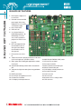
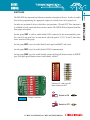
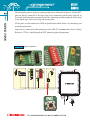
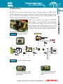
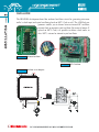
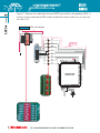
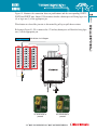
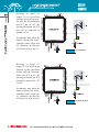
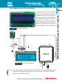
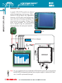
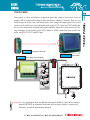
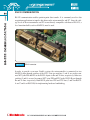
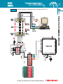
CONTENTS
BIGAVR2 KEY FEATURES
CONNECTING THE SYSTEM
INTRODUCTION
Switches
Jumpers
MCU Sockets
Power Supply
On-board USB 2.0 Programmer
Oscillator
LEDs
Reset Circuit
Push-buttons
2x16 Character LCD
Graphic LCD
Touch Panel
RS-232 Communication
A/D Converter Test Inputs
Direct Port Access
PS/2 Communication
JTAG
MMC/SD Memory Card
4
5
6
7
8
9
11
12
14
15
17
18
21
22
23
24
27
29
31
32
33
4
BIGAVR2 KEY FEATURES
BIGAVR2 KEY FEATURES
1. External power supply of 8v
to 16v AC/DC.
2. Selectable external and USB
power supply. When using
USB port, there is no need for
external power supply.
3. Power on/off switch.
4. USB connector.
5. Very fast and flexible onboard USB programmer. By
downloading a new software, it will be possible to
program new MCUs in coming years.
6. MCU card supports 64-pin
microcontrollers such as
ATmega128 and 100-pin
microcontrollers such as
ATmega1280.
7. Direct port access connector.
8. Jumpers to determine input pin performance in idle state
(connected to pull-up or pull-down resistor).
9. Switch group SW4 enabling pull-up/pull-down resistors
on port pins.
10. 86 push-buttons allowing control of all the microcontroller
pins.
11. Jumper to select high or low state of pins on any push-button
press.
12. RESET push-button.
13. Each I/O pin corresponds to one LED.
14. On-board clock oscillator.
15. LCD display contrast potentiometer.
16.
17.
18.
19.
20.
21.
22.
23.
24.
25.
26.
MMC/SD (MULTIMEDIA CARD) reader.
A/D converter test inputs.
Touch panel controller.
PS/2 keyboard communication port.
RS232 communication port.
GLCD display contrast potentiometer.
Touch panel connector.
GLCD connector.
LCD connector.
On-board reference voltage 4.096V.
JTAG connector.
Apart from this manual, the development system box contains development system, product
CD, USB cable, RS232 cable and user's manuals for AVRflash programmer, mikroICD Debugger and Installing USB drivers. In order to use BIGAVR2 properly, it is necessary to go
through the following steps:
Step no.1
Take the development system and product CD out of the box. Insert the
product CD into CD drive. Please, do not connect the development system
to a PC yet.
Step no.2
Install AVRflash programmer software to enable a program to be transferred
from PC to the microcontroller chip. Installation instructions are contained
in ‘AVRflash programmer’ manual.
Step no.3
Install USB drivers on your PC to enable programmer's hardware to operate properly on BIGAVR2 board. For detailed installation instructions
refer to 'Installing USB drivers' manual.
Step no.4
Connect BIGAVR2 to PC using USB cable. Please use one of USB ports
on the back of the PC because they are directly connected to the computer
motherboard.
The first time you switch the BIGAVR2 on, your PC will automatically
detect a new hardware. You will be immediately prompted whether Windows should search for new drivers update or not. Select the option 'No, not
this time' and click 'Next'. Another window appears, click 'Next' and the
operating system will automatically find the drivers. Click 'Finish' to complete this process and run AVRflash as explained in ‘AVRflash programmer’
manual.
Next time you switch the BIFGAVR2 on, Windows will not ask for new
drivers update during driver installation.
.
After these four steps, your BIGAVR2 is successfully installed and ready for use. You can read
a program from the chip or write a new one into it. The product CD provides numerous simple program examples which will make your first steps Easy...
.
5
CONNECTING THE SYSTEM
CONNECTING THE SYSTEM
INTRODUCTION
6
INTRODUCTION
The BIGAVR2 development system is a full-featured development board for Atmel AVR
microcontrollers. It is designed to allow students and engineers to easily test and explore the
capabilities of these AVR microcontrollers. In addition, it allows AVR microcontrollers to be
interfaced with external circuits and a broad range of peripheral devices. The user can therefore concentrate on software development only.
Figure 1 illustrates the development board. There are identification marks beside each component on a silkscreen, both on the top and bottom. These marks describe connections to the
microcontroller, operation modes, and provide additional useful information. Since all relevant information is provided on the board, there is almost no need for additional schematics.
Figure 1
BIGAVR2 development board
SWITCHES
7
Switches are mechanical devices which have two positions - ON and OFF. Their function is
to establish or break connection between two contacts. The BIGAVR2 development board has
four groups of switches.
Switch group SW1 is used to enable/disable LEDs connected to the microcontroller ports.
Five out of eleven ports have its own switch, while the ports F, G, H, J, K and C share three
lower switches of this group.
Switch group SW2 is used to enable/disable touch panel and MMC card reader.
Switch group SW3 is used to enable/disable RS232 communication.
Switch group SW4 is used to enable/disable external pull-up/pull-down resistors on PORTF
pins. Each pull-up/pull-down resistor is individually enabled.
Switches 1,2,3 and 4 are ON,
other switches are OFF
Switch is ON
Figure 2
Group of 8 switches
Switch is OFF
SWITCHES
The BIGAVR2 development board features a number of peripheral devices. In order to enable
them before programming, the appropriate jumpers or switches have to be properly set.
JUMPERS
8
JUMPERS
Jumpers, like switches, are used to break or establish connection between two points. Under
the plastic cover of a jumper, there is a metal contact which establishes connection when the
jumper is placed over two pins.
Jumper is ON
Jumper is OFF
Figure 3
Jumper as a switch
Jumpers are commonly used as selectors between two possible connections via 3-pin connector. As illustrated in figure 4, the middle connector pin can be connected to the left or right
pin, depending on the jumper’s position.
Jumper is not placed and
middle pin is unconnected
Figure 4
Jumper is placed on the left side
connecting middle and left pin
Jumper as a multiplexer
Jumper is placed on the right side
connecting middle and right pin
MCU CARD
BIGAVR2 is delivered with the 64-pin microcontroller ATmega128. The user can remove
MCU card with this chip and fit another MCU card with another microcontroller such as
ATmega1280 (100-pins).
Figure 5 MCU card
When placing MCU card on the BIGAVR2 MCU socket, it is necessary to follow steps
below:
Step no. 1
Step no. 2
Step no. 3
If MCU card is already placed on
BIGAVR2, you should remove it by
slowly pulling it up.
Place another MCU card on
the board. Note that label on
the MCU card must be in the
upper-left corner as it is drawn
on the BIGAVR2 board.
When the MCU card is properly
placed, push it down by applying pressure on all edges at the
same time.
MCU CARD
9
10
Microcontroller pins are routed to various peripherals as illustrated in figure 6. All the MCU
ports are directly connected to 2x5 direct port access connectors placed on the right side of
the board. Such connectors are normally used for connecting external peripherals to the board
or for digital logic probes for testing and measurement.
MCU CARD
All the ports are also connected to LEDs and push-button which allows easy monitoring and
testing digital pin state.
Some pins are connected to other peripherals such as RS-232 communication, Precise Voltage
Reference, LCD etc. which depends on MCU internal peripheral organization.
Figure 6
System connection
POWER SUPPLY
BIGAVR2 can use on of two power supply sources - PC power supply over USB cable (by
default) and external power supply (external AC/DC power adapter). When using power supply over USB, the system should be connected to PC using the USB programming cable,
while the jumper J14 should be set in right-hand position.
When using external power supply, the BIGAVR2
board produces +5V using LM7805 voltage regulator.
The external power supply can be AC or DC, while
power supply voltage ranges from 8V to 16V. The
jumper J14 should be set in left-hand position. Figure 8
illustrates USB and external power supply connectors.
Figure 7
Power supply connector
Figure 8
J14 is set to USB power supply
J14 in left-hand position: system
is powered from external AC/DC
power adapter.
J14 in right-hand position: system
is powered from PC via USB
cable.
POWER SUPPLY
11
ON-BOARD USB 2.0 PROGRAMMER
12
ON-BOARD USB 2.0 PROGRAMMER
There is no need to use external equipment
during programming as the BIGAVR2
development system has its own on-board
USB 2.0 programmer. It is only needed to
connect the system to PC using the USB
cable. Then, the program should be loaded
into the microcontroller using the AVRflash
programming software supplied with
BIGAVR2.
Please refer to AVRflash documentation for
more information.
Figure 9 USB 2.0 programmer
Figure 10 Programmer circuit diagram
Note:
There is no need to reset MCU after programming because the programmer will
reset the MCU automatically.
J20
J21
J20
J21
Figure 11
PE0, PE1 and PB1 used as programming lines
(Default) for 64-pin MCUs.
Figure 12
PB2, PB3 and PB1 used as programming lines
for 100-pin MCUs.
13
ON-BOARD USB 2.0 PROGRAMMER
There are two different groups of AVR MCUs (64- and 100-pin microcontrollers). The first
group (Default) uses jumper groups J20 and J21 for programming: PDI (PE0 pin), PDO (PE1
pin) and SCK (PB1 pin). See Figure 11.
Another group uses SPI communication lines for programming: MOSI (PB2 pin), MISO (PB3
pin) and SCK (PB1pin). See Figure 12.
OSCILLATOR
14
OSCILLATOR
The BIGAVR2 development board has on-board oscillator circuit for generating microcontroller’s clock input and crystal oscillator placed on MCU Card as well. The AVRFlash programmer enables you to choose between internal RC oscillator,
external clock or internal crystal oscillator. By means of jumper J1
(placed on MCU Card) it is possible to choose clock source to
drive MCU: external or internal crystal oscillator.
Figure 13 On-board oscillator
Figure 14 MCU Oscillator
Figure 15 Oscillator circuit diagram
Light Emitting Diodes (LEDs) are components most commonly used for displaying pins’ digital state. BIGAVR2 has 86 LEDs connected to the microcontroller ports: PORTA, PORTB,
PORTC, PORTD, PORTE, PORTF, PORTG, PORTH, PORTJ, PORTK and PORTL.
Figure 16 On-board LEDs
The development system is capable of monitoring the state of eleven MCU ports. Each of
these ports is connected to eight LEDs which can be enabled or disabled using switches of the
switch group SW1. The only exception is port PORG connected to six LEDs.
LEDs are enabled when the corresponding switch of the SW1 is ON. When enabled, LEDs
display the state of the corresponding microcontroller pin. Otherwise, the LEDs are always
off, no matter what the port state is, as no current can flow through them.
15
LEDS
LEDs
LEDS
16
Figure 17 illustrates the connection between PORTF pins and the corresponding LEDs. A
resistor is serially connected to LEDs in order to limit their current. In this very case the resistor value is 1K.
Figure 17 LEDs circuit diagram
RESET CIRCUIT
17
RESET CIRCUIT
In addition to other push-buttons, there is one red button on the far left portion of the boad
marked as RESET. It is used for MCU reset.
Figure 18 Reset button
As seen in figure below, the microcontroller MCLR pin is connected to programmer circuit
instead of being directly connected to RESET button.
Figure 19 Reset circuit circuit diagram
18
PUSH-BUTTONS
PUSH-BUTTONS
BIGAVR2 has 86 push-buttons used to change the state of digital inputs on the microcontroller
ports. There is also one RED push-button which acts as a RESET.
Figure 20 Push-buttons
When button is released the pin state is determined by pull-up or pull-down resistors.
Referring to Figure 21, J12 is connected to +5V and any button press will therefore bring logic
one (1) to the appropriate pin.
Figure 21
Push-button circuit diagram
5V while button is
pressed
0V while button is
pressed
19
PUSH-BUTTON
Figure 21 illustrates the connection between push-buttons and the corresponding PORTC,
PORTA and PORTF pins. Jumper J12 determines whether a button press will bring logic zero
(0) or logic one (1) to the appropriate pin.
PUSH-BUTTONS
20
Referring to figure 22,
jumper J3 is set to pull-up
position so that pull-up resistor pulls the microcontroller
pin PC2 pin to +5V. By
pressing the button, the PC2
pin will be connected to
ground via J12.
Accordingly, only when the
button is pressed the microcontroller senses a logic zero
(0). Otherwise, the pin state
will always be logic one (1).
Figure 22 pull-up position
Referring to Figure 23,
jumper J3 is set to pull-down
position so that pull-down
resistor pulls the microcontroller pin PC2 to 0V. By
pressing the button, the PC2
pin will be connected to +5V
via J12.
Accordingly, only when the
button is pressed the microcontroller senses a logic one
(1). Otherwise, the pin state
will always be logic zero (0).
Figure 23 pull-down position
2X16 CHARACTER LCD IN 4-BIT MODE
A standard character LCD is probably
the most widely used data visualization
component. It normally can display messages in two lines, each containing up to
16 alphanumeric characters. Characters
are made up of 5x8 pixels. The character
LCD communicates with the microcontroller via 4-bit data bus. Connecting to
the microcontroller is shown in figure 25.
Figure 24 2x16 LCD in 4-bit mode
Figure 25 2x16 LCD circuit diagram
Note: It is very important to bear in mind that LCD should be placed on or removed from the
BIGAVR2 development board only after the power supply is switched off. Otherwise,
it could be permanently damaged.
2X16 CHARACTER LCD IN 4-BIT MODE
21
GRAPHIC LCD
22
GRAPHIC LCD
A graphic LCD (GLCD) provides an advanced
method for displaying visual messages. While a
character LCD can display only alphanumeric
characters, a GLCD can be used to display messages in the form of drawings and bitmaps. The
most commonly used graphic LCD has 128x64
pixels screen resolution. The GLCD contrast
can be adjusted using the potentiometer P3
placed right above the touch panel controller.
Figure 26 GLCD
Figure 27 GLCD circuit diagram
Note: It is very important to bear in mind that GLCD should be placed on or removed from
the BIGAVR2 development board only after the power supply is switched off. Otherwise, it could be permanently damaged.
TOUCH PANEL
Touch panel is a thin, self-adhesive, transparent panel that could be placed over screen of
graphic LCD. It consists of two separate foils which form “sandwich” structure. They are very
sensitive to press so that even a soft touch causes some changes on output signal. It is used in
various user-friendly devices in combination with graphic LCD. Connector CN12 enables this
device to be connected to on-board touch panel controller whose active part consists of 5 discrete transistors. Four switches of the SW2 enable or disable connection between this controller and PF0, PF1, PG3 and PG4 pins.
Figure 28 Touch panel connector
Figure 29
Figure 30
Touch panel
Touch panel circuit diagram
Note: It is very important to bear in mind that touch panel should be placed on or removed
from the BIGAVR2 development board only after the power supply is switched off.
Otherwise, it could be permanently damaged.
TOUCH PANEL
23
RS-232 COMMUNICATION
24
RS-232 COMMUNICATION
RS-232 communication enables point-to-point data transfer. It is commonly used in data
acquisition applications to transfer data between the microcontroller and PC. Since the voltage levels of the microcontroller and PC are not directly compatible with those of RS-232, a
level transition buffer, such as MAX232, must be used.
Figure 31
RS232 connector
In order to provide even more flexible system, the microcontroller is connected to two
MAX232 chips through switches of the SW3. First two switches (1 and 2) are used to connect MCU pins PE0 and PE1 to the RS232-A port via Rx and Tx lines, respectively. Other two
switches (5 and 6) are used to connect MCU pins PD2 and PD3 to the RS232-B port through
Rx and Tx lines, respectively. Both RS232 ports have RTS and CTS lines (3 and 4 on RS232A and 7 and 8 on RS232-B) for implementing hardware handshaking.
25
RS-232 COMMUNICATION
Figure 32 Connection between microcontroller and PC through the RS-232A
RS-232 COMMUNICATION
26
Figure 33 Connection between microcontroller and PC through the RS-232B
A/D CONVERTER TEST INPUTS
The BIGAVR2 development board has two potentiometers for demonstrating the operation of
analog-to-digital converter (ADC). Both potentiometers outputs are in the range of 0 - 5V.
These analog signals can be connected to two different analog input pins at the same thime.
Jumper group J18 enables connection between potentiometer P1 and one of the following
pins: PF0, PF1, PF2, PF3 or PF4. Jumper group J19 enables connection between potentiometer P2 and one of the following pins: PF1, PF2, PF3, PF4 or PF5.
Figure 34 A/D converter inputs
In order to measure analog signal without interference, it is necessary to turn off the corresponding switch of the SW4. This disables connection between PORTF pins and pullup/down resistors.
A/D converter has a wide range of applications. The microcontroller takes analog signal from
its input pin and converts it into digital value. Basically, it is possible to measure any analog
signal that fits in the range acceptable by the microcontroller. In case of AVR, that range is 0 - 5V.
A/D CONVERTER
27
28
A/D CONVERTER
Pull-up/down resistors on
PORTF analog input pins
should be disabled using
the SW4
Figure 35 A/D Converter circuit diagram
NOTE: Jumpers J18 and J19 should not connect pins with the same labelat the same time.
DIRECT PORT ACCESS
All the microcontroller input/output pins can be accessed via 10-pin connectors (2x5) placed
along the right side of the board. For each microcontroller port there is one connector providing eight port pins for data transfer and two additional pins connected to VCC and GND.
Figure 36 Direct port access connectors
These connectors can be used to connect the system to external devices such as Serial
Ethernet, Compact Flash, DAC, CAN, RTC, RS-485 etc. In case on-board and external
peripherals use the same pins, then on-board peripherals must be disconnected from the
microcontroller by setting the appropriate jumpers. The connectors can be also used for
attaching logic probes or other test equipment.
Figure 37 Connecting external peripheral via flat cable
DIRECT PORT ACCESS
29
DIRECT PORT ACCESS
30
Figure 39 PORTA
Figure 38 PORTA circuit diagram
PS/2 (KEYBOARD) CONNECTOR
PS/2 connector allows direct connection between BigAVR2 and
devices that use PS/2 communication, such as PC, keyboard or
mouse. For example, the microcontroller can be connected to a keyboard to capture pressed keys or to a PC to act as a keyboard. CLK
and DATA lines are used for data transfer. In this case, they should be
connected to pins PC1 and PC0 respectively.
J15 and J16 are in default
position (OFF). Connect them
in order to use PS/2 connector.
Figure 40 PS/2 connector
Figure 41 PS/2 circuit diagram
PS/2 KEYBOARD CONNECTION
31
JTAG CONNECTION
32
JTAG CONNECTOR
JTAG connector can be used as a serial programming interface or as a part of on-chip debugger. JTAG connector pin marked as nSRST is directly connected to the RESET push-button.
In that way, on-chip debugger is able to use the RESET push-button as external reset source.
Additionally, the debugger can pull the RESET pin low in order to reset the whole system.
The JTAG interface is accessed through the four microcontroller pins:
TCK:
TDO:
TMS:
TDI:
Test Clock
Test Data Out
Test Mode Select
Test Data In
Figure 42 JTAG circuit diagram
Figure 43 JTAG connection
MMC card is used as a storage media for a portable devices from which it can be easily
removed to enable data transfer to a PC. For example, a digital camera uses MMC card for
storing image files. Data can be easily transferred from MMC card to a PC using MMC reader. Modern computers, laptops and desktops usually have card readers with SD slots for reading MMC cards.
Microcontroller on the BIGAVR2 development board communicates with MMC card via SPI
communication.
In order to enable MMC card, it is necessary to select and turn on switches 5, 6, 7, 8 of the switch
group SW2. The BIGAVR2 power supply voltage is 5V DC, whereas the MMC card power supply voltage is 3.3V DC. Because of that, there is an on-board voltage regulator MC33269DT-3.3.
For the same reason voltage level on data lines connecting the microcontroller to MMC card must
be limited to 3.3V. It is done by means of resistor voltage dividers as shown in Figure 44.
Figure 44 MMC/SD circuit diagram
33
MMC/SD MULTIMEDIA CARD
MMC/SD (MULTIMEDIA CARD)
Jumper
for
selecting high or
low state of pins
on any pushbutton press
Reset circuit
Push-buttons
for simulating
pins high or
low state
Oscillator
LEDs
Connector
for LCD in 4bit mode
MMC/SD
slot for
multimedia card
Jumper for
selecting
external or
USB power
supply
External
power supply
of 8 to 16V
AC/DC
A-D converter
test inputs
GLCD connector
Jumper
for
pull-up/pulldown selection
SW3 enables
RS232 communication
Switch
4
enabling PortF
pull-up, pulldown
SW2
for
enabling touch
panel
and
MMC/SD
SW1 for turning ON or
OFF
the
LEDs on all
AVR ports
4.096V voltage reference
JTAG connector
GLCD contrast
potentiometer
PC keyboard connector
Touch panel controller
RS232 communication ports
BIGAVR2 supports both 64- Touch panel
connector
and 100-pin AVR MCUs
Very fast and flexible USB
2.0 programmer
BIGAVR2