1
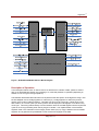
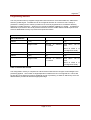
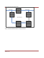
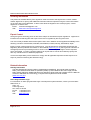
Duplex AES GCM 10G for OTN Core,
Xilinx Edition
January 21, 2015
Product Specification
Core Facts
Provided with Core
®
Algotronix
130-10 Calton Road
Edinburgh, Scotland
United Kingdom, EH8 8JQ
Phone: +44 131 556 9242
E-mail: [email protected]
URL:
www.algotronix.com
Documentation
User Manual
Design File Formats
VHDL or EDIF Netlist
Verification
Test Bench
Instantiation templates
VHDL
Simulation Tool Used
ModelSim
Support
Features
Support provided by Algotronix
• Implementation of AES-GCM with 96 bit IV
and 128 bit or 256 bit keys.
• Suitable for OTN and applications requiring AES-GCM with fixed packet sizes and relatively
infrequent key changes
• Compatible with all modern Xilinx FPGA families
• Independent 10Gbit transmit (encrypt) and 10Gbit receive (decrypt) channels sharing a single high
performance encryption engine
• Pass through functionality for packets not requiring encryption
• Comprehensive self-checking testbench
• Supplied as VHDL source code to allow security review
Applications
•
Wired, Optical and Wireless Networking
•
Network Test Equipment
•
OTN
General Description
The Algotronix AES-GCM Core implements the Galois Counter Mode (GCM) of operation of the
Advanced Encryption Standard (AES) algorithm. The AES-GCM mode of operation of AES was
originally described in a proposal by Cisco to the National Institute of Standards and Technology (NIST)
and later published as NIST Special Publication SP800-38D making it an officially endorsed mode of
operation of the AES cipher. The DUPLEX-AES-GCM-10G-FOR-OTN version of the product is
optimised for applications, such as OTN, where all packets are the same size and keys change relatively
infrequently. These characteristics allow significant area savings compared with our standard AESGCM-10G products for use in MACSEC and IPSEC.
AES-GCM is significantly more complex than the simple modes of AES such as ECB and CBC specified
in NIST special publication SP800-38A because unlike simple modes of the cipher which provide only
confidentiality, GCM provides both confidentiality and authentication. Authentication is the ability to
detect tampering with the encrypted message as it passes between the sender and receiver and in
5.1
Page 1 of 17
DUPLEX-AES GCM-10G-FOR-OTN Core
most applications is essential for security. GCM mode is based on the counter (CTR) mode of AES
which can be parallelized to achieve very high throughput. Thus GCM is the most suitable of the
standard modes of AES to provide both authentication and confidentiality for very high speed networks.
The DUPLEX-GCM-10G-FOR-OTN core is an area-optimised version of the standard AES-GCM-10G
core. Significant savings are obtained by sharing a single high performance encryptor across a transmit
and receive channel in the duplex configuration. Further area savings are obtained by having the user
precalculate the key schedule and information to simplify the hash computation in software and load
these pre-computed values into the core. This pre-computation approach only makes sense in
applications where the key changes relatively infrequently: in applications where the key changes
frequently (such as MACSEC or IPSEC) our AES-GCM-10G core which computes the keyschedule in
hardware is the appropriate choice. The core is further simplified by specifying a fixed length of packets
as a configuration parameter (rather than allowing packet length to vary as in the MACSEC and IPSEC
scenario) and limiting packet lengths to be an exact multiple of AES blocks (16 bytes or 128 bits) as will
naturally be the case for OTN frames. Algotronix can customise the core on request to lift some or all of
these restrictions.
The Duplex GCM 10G core operates with a fixed 96 bit IV and can be configured to use a 128 bit or 256
bit key. For simulation a self-checking configuration of the core checks the response of the
synthesisable code against a behavioral model. The user can instantiate this self-checking version of the
core in their own simulation in order to check its response to stimulation from their design and track down
any problems in the way the core is being driven more quickly. The core testbench uses the self
checking version of the product and stimulates it with a user specified number of randomly generated
vectors.
The DUPLEX-AES-GCM-10G-FOR-OTN core is supplied as VHDL source code and can be configured
using a number of VHDL generic parameters to select only those features which are required in order to
conserve area. The core is an easy to use fully synchronous design with a single clock. The core has
been designed for efficiency in modern FPGAs and makes full use of FPGA dual port memory blocks.
Implementation Statistics
Example implementation statistics for the duplex design are provided below: when comparing these
numbers against other implementations of AES-GCM please bear in mind that this core implements a
receive and a transmit channel which is twice as much encryption throughput as a unidirectional core.
The core can target all recent families of Xilinx chips and has a variety of configuration options,
Algotronix will run the core through FPGA vendor design tools and provide figures for devices and
options not listed in the tables below and on request. The design was run with a clock constraint of
156.25MHz which is required to deliver 10Gbit/sec throughput (on both channels simultaneously) and
with the slower -2 speed grade which was sufficient to meet the clock constraint. The 256 bit key
requires more pipeline stages and hence more resources than would be required with a 128 bit key.
Table 1: Example Implementation Statistics for AES-GCM, 256 bit Key, ‘Push Button’ flow with
Fmax specified by clock constraint. AES Sboxes implemented in block RAM.
Family
Example Device
Fmax
FF
LUT
(MHz)
Virtex-7
Page 2 of 17
XC7VX1140T-2
156.25
Memory GCLK BRAM
LUT
6201
8827
1798
(18K)
1
56
Throughput
Design
(GBit/sec)
Tools
10Gbit//sec
Vivado
per channel
2014.2
Algotronix
®
Functional Description
The main functional blocks are as shown in Figure 1, and explained below. The various I/O signals
shown on the diagram are defined in Table 2.
AES-GCM Compute Unit
The AES-GCM compute unit operates at twice the speed of the transmit and receive channels and is
time-multiplexed to serve both channels. The AES unit used to provide privacy has a fully unrolled
pipeline and starts an encryption on every clock cycle. The Galois Field multiplier required by the
GHASH algorithm used for authentication is pipelined and parallelised to match the throughput of the
AES unit.
The AES-GCM compute unit computes the value of the ICV based on input data for the transmit and
receive channels. It is the responsibility of user circuitry to calculate authentication success for the
receive channel by comparing the computed ICV and an ICV sent with the received data. In the OTN
application there is no standard specifying which field in the received data will be used to transmit the
expected ICV and it may be convenient to send the ICV for the current frame in a subsequent frame.
Therefore separating the authentication success computation from the AES-GCM unit provides more
flexibility. User circuitry must also ensure that if authentication is not successful the corresponding frame
is discarded.
Input Multiplexer
The transmit_input_cycle signal is generated by the control logic and toggles continuously. When
transmit_input_cycle = '1' the multiplexer routes data from the transmit channel to the AES-GCM
processing unit and when transmit_input_cycle = '0' it routes data from the receive channel.
Output Demultiplexer
The 128 bit output_text and output_tag outputs from the AES-GCM compute unit are not demultiplexed
into separate versions for the transmit and receive channels. It is more convenient to leave them timemultiplexed so that the core can be easily instanced into an FPGA on its own (128 bit wide buses for
each channel require too many pins to allow this). The associated single bit control signals are
demultiplexed into separate versions for each channel. SINCE A SINGLE OUTPUT IS SHARED
BETWEEN THE TRANSMIT AND RECEIVE CHANNELS THE USER CIRCUITRY INTERFACING
WITH THE CORE MUST ENSURE THAT DECRYPTED PLAINTEXT DATA OUTPUT FOR THE
RECEIVE CHANNEL CAN NEVER LEAK INTO THE TRANSMIT CHANNEL WHERE IT MIGHT BE
VISIBLE TO AN ATTACKER.
GCM Control and Precalculated Data Memory
This block contains a state machine that generates various control signals for the rest of the design
including the transmit_input_cycle signal used for time-multiplexing the AES-GCM compute unit. It also
contains a memory block to hold the precalculated data (including the AES key schedule) for each
channel. Each channel's memory has an active bank controlling the datapath and an inactive bank into
which the processor writes new data. When the transmit or receive key needs to be changed this
structure allows a new set of data to be installed by the processor while the datapath is running. The
transmit_activate_key or receive_activate_key signal are then pulsed high one clock before the
Page 3 of 17
DUPLEX-AES GCM-10G-FOR-OTN Core
transmit_first or receive_first signal starts a new packet, swapping the key over without interrupting
packet processing (note that the 'one clock cycle before' condition implies transmit_initialise_key is
pulsed high when transmit_input_cycle = '0').
Page 4 of 17
Algotronix
®
Figure 1, DUPLEX-AES-GCM-10G Core Block Diagram
Description of Operation
In the description below ‘block’ is used to refer to an AES block of 128 bits of data, ‘packet’ is used to
refer to an AES-GCM processing unit consisting of IV, AAD and plaintext or ciphertext (depending on
whether it is an encrypt or decrypt operation).
The DUPLEX-AES-GCM-10G-FOR-OTN core implements the AES portion of the algorithm using a 128
bit wide datapath and a 10 stage pipeline for 128 bit keys ( 14 stage pipeline for 256 bit keys which
require more rounds of AES processing). This AES unit can encrypt or decrypt a 128 bit block of text
with a latency of 10 clock cycles (14 clock cycles for 256 bit keys) and a throughput of one block every
clock cycle. This timing follows directly from the iterative nature of the AES algorithm which requires ten
cycles of inner loop processing when the key length is 128 bits. The implementation of the GHASH
algorithm used in the calculation of the Integrity Check Value (ICV) (or 'tag') is based on the Kurutsaba
algorithm and is pipelined and parallelised to offer the same throughput as the AES.
Page 5 of 17
DUPLEX-AES GCM-10G-FOR-OTN Core
The transmit and receive channels transfer data every second clock cycle for a throughput of 10
Gbit/sec. They are time multiplexed to share the 20Gbit/sec encryption compute unit based on the
transmit_input_cycle signal which is generated by the core and immediately following reset starts
toggling every clock cycle. When transmit_input_cycle = '1' data is transferred for the transmit channel
and when it is '0' data is transferred for the receive channel.
The core relies on user software to precompute information used in the AES GCM algorithm and load
that information into the precalculated data memory within the core through a processor interface
separate from the data interface which transfers packets. Writing information to the precalculated data
memory to set up a new key does not disturb normal operation of the core processing packets using the
information from the previous key. The user activates new keys by pulsing the transmit_activate_key (or
receive_activate_key) signal high on the clock cycle before the first packet to be processed with the new
key enters the core. The precalculated information includes the key schedule for AES encryption and the
value of H used in the GHASH algorithm.
Processing a packet of GCM data on the transmit channel is initiated by pulsing the transmit_first signal
high on a clock cycle where transmit_input_cycle = '1'. The first block of text, the transmit_pass_through
control signal and transmit_input_iv must be valid at this time. The transmit_pass_through and
transmit_iv signals are latched internally at this time and changes during period while the core is
processing data will have no effect. The receive channel works the same way except that the
corresponding receive_first, receive_input_text, receive_input_iv and receive_pass_through signals are
used and transmit_input_cycle is '0'. There may be a gap between the previous packet finishing and the
first signal for the next packet being activated but this is not required: it is possible for the next packet to
start on the next input cycle for the channel.
In this document the sequence of activity is described but the number of clock cycles between phases of
activity is not specified. Ideally, the user circuit should synchronize to the GCM core using the
output_valid signals rather than by assuming a set number of clock cycles between various operations.
Future updates to the core may have slightly different delays as a consequence of changes to improve
latency and/or throughput.
There are many possible timing scenarios depending the various configuration parameters for the core.
For reasons of space and convenience detailed timing charts for the different scenarios are not provided
in the product description but are produced on request using the testbench and supplied separately.
Page 6 of 17
Algotronix
®
Compilation Options
The core can be configured easily using a set of VHDL generic parameters. Normally, it is unnecessary
for users to modify the design source code although the code is supplied and they are free to do so if
they wish. Algotronix can also customise the core as a service for users with particular requirements
which are not met by the standard product.
•
aad_length_in_blocks - number of 128 bit blocks (16 byte) blocks of Additional Authenticated
Data (AAD) in each packet. The AAD precedes the text to be encrypted/decrypted and is
authenticated but not encrypted. AAD is useful for header information which must be
immediately accessible to intermediate nodes on the communications channel but protected
against tampering.
•
text_length_in_blocks - number of 128 bit blocks (16 byte) blocks of text (plaintext or
ciphertext) in each packet. The text is encrypted for privacy and authenticated.
•
processor_data_width - width of the data on the data_from_processor input, 16 or 32 bit data
busses are supported. This parameter also affects the width of the address_from_processor
input since more addressable words of data are required with a 16 bit word size.
•
implement_sboxes_in_ram - specifies whether the AES SBoxes are implemented using FPGA
RAM blocks or using FPGA LUT resources. This choice will have a major impact on the balance
of resources in the design and a significant effect on achievable clock frequency.
•
target_device – This edition of the core can target all families of Xilinx FPGAs. Alternative
editions target other FPGA manufacturers as well as a 'platinum' edition which can target all
leading FPGAs or ASIC. To achieve 10Gbit/sec performance the Xilinx Virtex 5 or later high
performance FPGA families are recommended. The core can be compiled to target lower
performance Xilinx FPGA families but the achievable clock frequency may not be sufficient for
10G throughput.
Page 7 of 17
DUPLEX-AES GCM-10G-FOR-OTN Core
Core I/O Signals
Descriptions of all I/O signals are provided in Table 2. In most cases these signals will connect to signals
in the surrounding user design, not directly to I/O pins on the FPGA.
The I/O signals for the duplex core differ from those on the AES-GCM-10G core as follows:
1. There are signals for two separate channels (transmit and recieve) where AES-GCM-10G has a
single channel which can be used for either transmit or receive. As a result there is an additional
transmit_ or receive_ prefix on many signal names in the duplex core.
2. There is no enable signal on this version of the core: when a packet is started by bringing the
receive_first or transmit_first signal high processing cannot be paused part way through so the
external circuitry must be ready to deliver the whole packet.
3. The core assumes the size of the AAD and text will always be an exact number of AES blocks,
as is the case for OTN. As a result the _width inputs and outputs used to specify the number of
bytes in the last block of AAD or text are not required.
4. The number of blocks of AAD and text is known in advance and specified as a configuration
parameter. Therefore there is no need for the _kind fields which specify whether the current
input or output text is AAD or text.
5. The end of the packet can be determined by counting input or output blocks since all packets are
a fixed size. Therefore there is no need for the _final signals on teh input and output side which
mark the final block of text.
6. There are no signals associated with loading keys since the key information is provided in
advanced through the processor interface.
7. The 'start' signal on AES_GCM_10G input side occurs one clock before the data and is used to
trigger calculation of the keyschedule is replaced with a 'first' signal which goes high concurrently
with the first data word.
8. A processor interface and transmit_install_key and receive_install_key signals are added to deal
with loading and enabling key dependent data.
Page 8 of 17
Algotronix
Signal
Signal
Description
Direction
clock
input
Clock – active on rising edge.
reset
input
Asynchronous reset – active high. For Xilinx FPGA implementation, unless
security considerations mandate an asynchronous reset, it is recommended to
specify that the reset signal is implemented synchronously in the synthesis tools.
This can result in reduced area and improved performance.
processor_write_
input
Indicates the data on the data_from_processor input should be written to the internal
precalculated data memory at the address specified in the processor_address
signal
input
Address of data to be written in the inactive bank of precalculated data memory. The
processor cannot access the memory bank which is currently controlling the
datapath. The width of the address bus depends on whether the core is compiled
with a 32 or 16 bit data bus.
enable
processor_address[5:0]
(or [6:0] with 16 bit
data bus)
data_from_
input
processor[31:0]
Data to be written to the precalculated data memory. 32 and 16 bit data busses are
supported.
(or [15:0] with 16 bit
data bus)
transmit_activate_key
input
Pulsed high one clock cycle before the transmit_first indicates the first block of a
new packet on the transmit channel to swap over the active and inactive banks of
precalculated data memory for the channel. The processor must have written all the
required data before this signal is asserted.
receive_activate_key
input
Pulsed high one clock cycle before the receive_first indicates the first block of a
new packet on the receive channel to swap over the active and inactive banks of
precalculated data memory for the channel. The processor must have written all the
required data before this signal is asserted.
transmit_input_cycle
output
The AES-GCM core inputs and outputs data every second clock cycle. This signal
allows external circuits to align with the input/output cycles of the AES-GCM core.
This signal continues in gaps between packets whereas the load_text signal is only
active when data is actually being transferred.
transmit_first
input
Pulsed high on the first block of transmit_input_text (i.e. transmit_input_cycle = '1')
for a new packet to be processed. The transmit_pass_through and
transmit_input_iv inputs are sampled and these parameters are fixed for the next
block of operations. There can be a gap between the last block of text of the
previous packet entering the core and this signal pulsing high to mark the start of
the new packet.
transmit_pass_through
input
Sampled when transmit_first = '1', specifies that the packet is to be passed through
the core without any security processing. This is a convenience feature so that the
user does not have to provide a separate path around the GCM.
transmit_input_iv
input
Data input. A complete 96 bit AES IV is transferred in a single clock cycle when
transmit_first = '1'.
[95:0]
transmit_input_text
input
Data input. A complete 128 bit AES block is transferred on the clock cycle when
transmit_input_cycle = '1'.
[127:0]
receive_first
input
Pulsed high on the first block of receive_input_text (i.e. transmit_input_cycle = '0')
for a new packet to be processed. The receive_pass_through and receive_input_iv
inputs are sampled and these parameters are fixed for the next block of operations.
There can be a gap between the last block of text of the previous packet entering
the core and this signal pulsing high to mark the start of the new packet.
receive_pass_through
input
Sampled when receive_first = '1', specifies that the packet is to be passed through
the core without any security processing. This is a convenience feature so that the
user does not have to provide a separate path around the GCM.
receive_input_iv
input
Data input. A complete 96 bit AES IV is transferred on the clock cycle when
Page 9 of 17
®
DUPLEX-AES GCM-10G-FOR-OTN Core
receive_first '1'.
[95:0]
receive_input_text
input
Data input. A complete 128 bit AES block is transferred in a single clock cycle.
[127:0]
transmit_output_
output
Valid flag – high when output_text is valid for the transmit channel.
text_valid
transmit_output_text_
output
High on the first block of output text for a packet on the transmit channel.
first
receive_output_
output
Valid flag – high when output_text is valid for the receive channel.
text_valid
receive_text_first
output_text
output
output
Data output: in the current version of the core this bus is 128 bits wide and the 128
bit block of text is transmitted in a single clock cycle.
output
High when output_tag is valid and contains the tag computed for the transmit
channel. This is several clock cycles after the final word of output_text for the
packet.
output
High when output_tag is valid and contains the tag computed for the receive
channel. This is several clock cycles after the final word of output_text for the
packet.
[127 : 0]
transmit_output_tag_
valid
receive_output_tag_
valid
output_tag
High on the first block of output text for a packet on the receive channel.
output
Output bus for the ICV computed from the ciphertext.
[127 : 0]
transmit_output_pending
R receive_output_pending
output
output
Table 2: Core I/O Signals.
Page 10 of 17
Indicates that the core is currently processing input data and there will be further
transmit_output_valid cycles.
Indicates that the core is currently processing input data and there will be further
receive_output_valid cycles.
Algotronix
®
Programming Interface
The core provides memory mapped configuration resources with a conventional data bus, address bus
and write_enable signal. The data bus can be configured as either 16 or 32 bits to suit a variety of
processors. Reading back of memory locations is not currently supported since it would be relatively
expensive in FPGA resources. Algotronix can provide a readback capability on request. An additional
address bit is provided for the 16 bit processor interface since the smaller data bus width requires more
words of addressable memory to provide the required information.
Address Bus Format
with 32 bit data bus
Address
(7:3)
(2)
(1:0)
Stage number
Channel : 0 = transmit,
1 = receive
Word within
block.
128
bit
(Word at offset 0 is
most significant word).
with 16 bit data bus
Address
(8:4)
(3)
(2:0)
Stage number
Channel : 0 = transmit,
1 = receive
Word within
block.
128
bit
(Word at offset 0 is
most significant word).
Table 3: Address Bus Format.
The configuration memory is composed of 128 bit blocks of data used to configure various stages in the
processing pipeline. The number of stages depends on whether the core is configured for a 128 or 256
bit AES key since 256 bit keys require additional rounds of processing: to allow for 256 bit keys a five bit
address field is provided to select the appropriate stage.
Page 11 of 17
DUPLEX-AES GCM-10G-FOR-OTN Core
128 bit key stages
0 .. 10
AES round key 0..10.
(Round key 0 is the
input key).
11..13
Precomputed GHASH
information 0..2
256 bit key
0..14
AES round key 0..14.
(Round key 0 is the 128
MS bits of the key).
15..17
Precomputed GHASH
information 0..2
Table 2: Stage Memory Format.
High level behavioral VHDL code to compute the required AES round keys and precomputed GHASH
information for loading into the memory is provided with the core as part of the testbench and can easily
be translated to C.
The processor can configure the channels independently: when changing a key for one channel there is
no need to write the information for the other channel. Information written to the configuration memory
goes into a separate memory bank from that used to control the datapath and does not disturb datapath
operation. Complete configuration information for the channel must be written before asserting
transmit_activate_key or receive_activate_key to swap the new information into the active memory bank
controlling the hardware.
The compute unit consists of a series of pipeline stages. When a new key is activated and a new packet
started as the first data for the new packet makes its way through the pipeline the earlier pipeline stages
will be operating with the new key but the later pipeline stages will still be processing the previous packet
and using the previous key. There is a period of 18 clock cycles for a 256 bit key (or 14 clock cycles for
a 128 bit key) immediately following the transmit_activate_key or receive_activate_key pulse during
which this transition is occurring and the user must take additional care when writing to the control
memory. A write to a memory stage which is not yet swapped over to the new key will leave the core
incorrectly configured resulting in errors. Two simple strategies are available to prvent this happening:
a. Wait for 18 clocks after the transmit_activate_key or receive_activate_key pulse before starting to
write new information so that the transition is complete for all stages.
b. Write the new information in order starting with stage 0 and working in sequence to the last stage.
With a 16 or 32 bit databus the processor will take several write cycles for each 128 bit stage (whereas
the hardware will flip over a complete stage every clock) the processor will always be working on stages
that the hardware has already dealt with.
This is an important practical consideration in simulation where it is easy for a testbench to write key
information every clock. However, configuration of the core in hardware from software running on an
embedded processor is unlikely to be fast enough to trigger the problem.
Page 12 of 17
Algotronix
®
Verification Methods
The testbench includes a self-checking configuration of the top level entity in the VHDL design which
uses the behavioral model of the AES-GCM algorithm to check the results from the synthesisable
implementation code. This is implemented using the VHDL facility to provide multiple architecture
definitions for a particular entity: the top level entity in the design has a self_check and a synthesis
architecture defined. As shown in Figure 2, the self checking architecture has an identical interface to
the synthesisable architecture and instances the synthesisable architecture within itself but also contains
behavioral code to capture all input and output signals and check their values against expected values
computed using a behavioral model. When errors are detected assertions are triggered and the
simulation is stopped with an error message.
This self-checking configuration of the DUPLEX-AES-GCM-10G-FOR-OTN core can be instantiated
within the user's own simulations. This makes it easy to verify the core operates properly when
connected to the user circuitry surrounding the core. The assertions within the self checking code will
detect and report most situations where the user design is not driving the core correctly simplifying the
task of integrating the core with the larger user design easier.
The DUPLEX-AES-GCM-10G-FOR-OTN testbench supplied with the core also makes use of the self
checking configuration of the core. The testbench stimulates the self checking core with a random
sequence of packets, writes of key information and key activations and the self checking core takes
responsibility for detecting any errors.
To verify the AES-GCM behavioral model used in the self checking duplex core it is checked against the
simpler AES-GCM behavioral model from the AES-GCM-10G core. The AES-GCM-10G core behavioral
model has itself been verified using NIST known answer tests and known answer tests produced from
well known software implementations of AES GCM.
Page 13 of 17
DUPLEX-AES GCM-10G-FOR-OTN Core
Figure 2, DUPLEX-AES-GCM-10G Self Checking Architecture
Page 14 of 17
Algotronix
®
Recommended Design Experience and Security Considerations
It is recommended that the user is familiar with the VHDL language and with the Xilinx design flow and
simulation tools. The core can also be instantiated inside a wrapper to allow use with a Verilog design
flow.
It is also recommended that the user has a background in data security or takes appropriate advice when
considering how to implement DUPLEX-AES-GCM-10G-FOR-OTN in a larger system.
A specific security consideration for the AES-GCM algorithm is that the system must ensure that the
counter created from the 96 bit IV and 32 bit internal counter can never wrap round so that the same
counter value is used twice with the same key. The usual response to detecting that the counter is
about to wrap round is to shut down the link until the a new key is installed.
A second security consideration is that a mechanism should be included to detect packet replay (i.e.
resending a copy of a valid packet), one way to do this is a packet counter which is expected to increase
in value on each received packet. The packet counter can also be used to form part of the IV. Packet
replay will not be detected by the authentication mechanism in AES-GCM because the replayed packet
will have a valid ICV.
If an incoming packet on the receive channel fails authentication (computed ICV does not match
expected ICV transmitted with the packet) it must be discarded and not passed on to higher layers in the
communication system which may act on it.
Page 15 of 17
DUPLEX-AES GCM-10G-FOR-OTN Core
Ordering Information
This product is available directly from Algotronix under the terms of the SignOnce IP License. Please
contact Algotronix for pricing and additional information about this product using the contact information
on the front page of this datasheet. To learn more about the SignOnce IP License program, contact
Algotronix or visit the web:
Email:
URL:
[email protected]
www.xilinx.com/ipcenter/signonce
Export Control
Strong encryption technology such as AES is the subject of international export regulations. Algotronix is
located in the United Kingdom and export of this core is regulated by the UK government.
The core is freely available within the European Union and in addition can be supplied immediately to the
following countries: United States, Australia, New Zealand, Canada, Norway, Switzerland, Japan.
Export to other countries requires an export licence. The UK Department of Business, Enterprise and
Regulatory Reform publishes information on their website (www.berr.gov.uk) which gives an indication of
average export licence processing times for various countries and the percentage of licence requests
which are granted. For many countries obtaining an export licence can be done relatively quickly and
with only a small amount of additional paperwork.
It is the the responsibility of the customer to comply with all applicable requirements with respect to reexport of products containing the AES technology.
Related Information
Industry Information
The AES standard documents FIPS197, SP800-38A and AESAVS, the original GCM proposal to
NIST (“The Galois/Counter Mode of Operation (GCM)” by David McGrew and John Viega) and the
NIST special publication SP800-38D document describing GCM mode are available from the National
Institute of Standards and Technology, Computer Security Resouce Center website
(www.csrc.nist.gov).
Xilinx Programmable Logic
For information on Xilinx programmable logic or development system software, contact your local Xilinx
sales office, or:
Xilinx, Inc.
2100 Logic Drive
San Jose, CA 95124
Phone: +1 408-559-7778
Fax:
+1 408-559-7114
URL:
www.xilinx.com
Page 16 of 17
Algotronix
®
Copyright © 2002-2015 Algotronix Ltd., All Rights Reserved.
®
Algotronix is a registered trademark of Algotronix Ltd. in the United States and United Kingdom and a
trademark of Algotronix Ltd. in other countries.
The supply of the product described in this document is the subject of a separate license agreement with
Algotronix Ltd. which defines the legal terms and conditions under which the product is supplied. This
product description does not constitute an offer for sale, a warranty of any aspects of the product
described or a license under the intellectual property rights of Algotronix or others. Algotronix products
are continuously being improved and are subject to change without notice. Algotronix products are
supplied ‘as is’ without further warranties, including warranties as to merchantability or suitability for a
given purpose. Algotronix’ products are not intended for use in safety critical applications.
URL: www.algotronix.com
Version Control Information
Subversion Revision Number
Date
Document
Status (blank field indicates OK/no warnings)
63
2015/01/23 09:55:24
Duplex AES GCM 10G For OTN Data Sheet, Xilinx Edition
(Table auto-updates, do not edit field values by hand)
Page 17 of 17