1
United States Patent [191
Louie et al.
[54]
INTERFACE BETWEEN A
MICROPROCESSOR AND A COPROCESSOR
[76] Inventors: glennéiom‘j’. 274g
Reotren
Patent Number:
Date of Patent:
[11]
[45]
4,547,849
Oct. 15, 1985
Attorney, Agent, or Firrn~0wen L. Lamb
[57]
ABSTRACT
R?
A nonclock-synchronous interface between a micro
Ag‘; “22:61am St’ 2:6“:
processor and a coprocessor. A request line (404) from
Shaman Hair: 32714 Israel’ ‘:Imes
slag“ 6’230 Pasos Lo’s cerri’tos San
the coprocessor and an acknowledgment line (402) from
the microprocessor provide for operand transfer from
Jose éalif 95120
’
’
the coprocessor to the microprocessor. A busy line
'
(410) and an error line (408) from the coprocessor allow
[21]
[22]
APPI- NW 615,081
Filed:
Aug 17 1984
’
Related U 5 Application Data
[63]
Continuation of Ser. No. 328,973, Dec. 9, I981, abandoned'
cumvemed_ A m¢mory_read cycle is generated using
the address taken from the memory-address register
[51]
[52]
Int. Cl.‘ ............................................ .. G06F 15/16
[1.8. CI. . ................................................. .. 364/200
(401) The data is buffered inside the microprocessor
and the coprocessor’s request is acknowledged. The
[58]
56
Field of Search 364/200 MS File, 900 MS File
R f
Cited
I 1
e erences
US. PATENT DOCUMENTS
3,940,743 2/1976 Fitzgerald ......................... .. 364/200
memory-address register is then incremented by a pre
determined amount and an I/O write cycle is generated
using a prewired address into the coprocessor. Data are
transferred in the opposite direction in a similar manner
_
4,006,466
I
the microprocessor to monitor the condition of the
coprocessor. Data (406) are transferred through a data
channel in the microprocessor using the full memory
management and protection mechanism of the micro
' '
processor so that the protection mechanism is not cir
“Sing the prewired address ‘0 Obmi" ‘he read data from
2/1977 Patterson at at H
____ _, 364/200
the coprocessor which data is buffered inside of the
4,099,236 7/1978 Goodman et al.
4,106,092 8/1978 Millers, III ...... ..
.... .. 364/200
364/200
microprocessor. A memory-write cycle is then gener
ated by the processor using an address taken from the
- t - - ~~
channel memory-address register and the data equal to
,
¥°EFT ----
y
0
4,365,294 12/1982
~- - - -
1T3 Cl a .
.... ..
Stokken ............................. .. 364/200
the dam buffered‘
Primary Examiner-Eddie P. Chan
4 Claims, 6 Drawing Figures
BUS UNlT
200
F ” ' ‘ ‘ ‘ ' ' 'z'ls" _ iiionatss
“OM55 —L—-{| ADDRESS mums,L
um
I
2:4
l
20?;_
: PREFETUNER
'
2/[2
_
_
_
_
_
_
/
CDPROCESSOR
Q‘2.0 : 408
i 7 "m1
I 4,0 BUSY
i
_
1
'°°RE°\ r404
I um COPROCESSOR
1 am CHANNEL
c
40o
WW ‘4
ONTR [LI 5
_
_
_
__
_
p
4|2"
EXECUTION UNIT
m
INSTRUCTION UNIT
m
____ NAIN NENURY
m
U.S. Patent Oct. 15, 1985
Sheet 1 of5
4,547,849
3
1|Isi?w
£22":
021
2;E;N?.n
21,_(a25E;3Z2,_Q8“n4292%EN2;2:I5 E_52w% “"U23£80asE8212:H53E20::3_2525 323E?aJJ__
2:3_2:at2?
.OE
_
| 2:E502:;3%5
mm.N3.mic“
U.S. Patent Oct.l5, 1985
FIG.5
Sheet4of5
4,547,849
SET START/
450~ STOP FLAG
T0"STOP"
LOAD MEMORY
454~ ADDRESS LIMIT
REGISTER
SET USER / ICE
FLAG TO "USER"
SET DIRECTION
460~ FLAG TO
"MEMORY TO
SLAVE"
SET START
464~ STOP FL
T0 "STAR "
SET USER / ICE
FLAG T0 "ICE"
SET DIRECTION
MEMORY"
1
4,547,849
INTERFACE BETWEEN A MICROPROCESSOR
AND A COPROCESSOR
This application is a continuation, of application Ser.
No. 328,973, ?led Dec. 9, 1981, now abandoned.
BACKGROUND OF THE INVENTION
1. Field of the Invention
The present invention relates to microprocessors, and
more particularly, to apparatus for controlling the
movement of data to and from a slave coprocessor.
2. Description of the Prior Art
In US. Pat. No 4,442,484 of Robert Childs, Jr., et al
entitled “Microprocessor Memory Management and
Protection Mechanism,” granted on Apr. 10, 1984, and
assigned to a common assignee, Intel Corp., there is
described a memory management and protection mech
2
address therein corresponding to a main memory ad
dress is connected to the address bus. An I/O address
register is also connected to the address bus. The 1/0
address register contains a ?xed address therein corre
sponding to an I/O address of the coprocessor reserved
for data transfers to and from the main memory. A data
buffer register is connected to the data bus. The control
logic is responsive to the COREQ signal line for trans
ferring data from the main memory to the data register
during a ?rst cycle, the data being read from an address
in main memory corresponding to an address stored in
the memory address register. The transferring means
includes means for energizing the COACK# signal line
to acknowledge the coprocessor request during the ?rst
cycle. An incrementer responsive to the control means,
operative during the ?rst cycle, increments the contents
of the memory address register. Means responsive to
the control means, operative during a second cycle,
anism in which access to protected entitites is con
trolled. The memory-protection mechanism provides 20 places the read data in the data buffer register on the
protection of a task from other tasks, protection of a
data bus and places the address in the I/O address regis
segment at one level from any task at a less privileged
ter on the address bus. This transfers the data to the
coprocessor.
violations.
Data are transferred from the coprocessor to main
It is desirable to utilize the microprocessor described 25 memory via the data channel in the following manner.
in the Childs, et a] patent application as a master micro
The control logic is responsive to the COREQ signal
level, and immediate detection of attempted protection
processor with a slave coprocessor, such as an 8087
Math Processor, with the coprocessor being subject to
line for transferring data from the coprocessor to the
data register during a ?rst cycle, the data being read
the same protection rules as the master microprocessor.
from an address in the coprocessors memory corre
In order to do this, it is necessary to provide an interface 30
sponding
to an address stored in the [/0 address regis
which will allow the transfer of operands between the
ter. The transferring means includes means for energiz
attached coprocessor and main memory without cir
ing the COACK# signal line to acknowledge the co
processor request during the ?rst cycle. Means respon
Prior to the development of large-scale integration 35 sive to the control means, operative during a second
cycle, places the read data in the data buffer register on
(LSI) technology, the interfaces between computer
the data bus and places the address in the memory ad
components were mainly concerned with transferring
dress register on the address bus. This transfers the data
data at the highest speed possible commensurate with
to the main memory. An incrementer responsive to the
the electrical characteristics of the cables between the
control means, operative during the second cycle, in
units and the electronic circuits which drive signals on
cumventing the protection mechanism in the micro
processor.
the cables. The use of these prior interfaces with LSI
microprocessors is prohibitive because there are not
enough input/output pins available on the LS1 package
with present-day technology. An LSI microprocessor
crements the contents of the memory address register.
The invention has the advantage that data transfers
are fully memory protected because the data to and
from the slave coprocessor are transferred indirectly to
has to use fewer actual lines interconnecting the mod 45 and from main memory via the master processor memo
ules, but still meet the requirement of being able to
ry-protection mechanism.
handle data movement and control operations just as
BRIEF DESCRIPTION OF THE DRAWINGS
It is therefore a primary object of this invention to
The foregoing and other objects, features, and advan
provide an interface between a master microprocessor 50 tages of the invention will be apparent from the follow
and a slave coprocessor which utilizes a minimum num
ing detailed description of a preferred embodiment of
ber of input/output pins and which does not circumvent
the invention as illustrated in the accompanying draw
the memory-protection mechanism of the master micro
ings wherein:
processor.
FIG. 1 is a functional block diagram illustrating the
55
various components of a microprocessor in which the
BRIEF SUMMARY OF THE INVENTION
invention is embodied;
Brie?y, the present invention is concerned with an
complex as those of previous data processing systems.
interface between a master microprocessor and a slave
coprocessor which share a memory address bus and
data bus connected to a main memory. The coprocessor
FIG. 2 is a more detailed block diagram of the bus
unit shown in FIG. 1;
FIG. 3 is a timing diagram illustrating bus cycle tim
1118;
has means capable of reserving an I/O address dedi
FIG. 4 is a timing diagram illustrating COREQ deac
cated to data transfers between the master microproces
tivation, asynchronous inputs, hold acknowledge, and
sor and the slave coprocessor. The master microproces
reset;
sor has a data channel comprising control logic con
FIG. 5 is a logic ?ow chart of the data channel initial
nected to a ?rst signal line from the coprocessor to the 65
ization sequence; and
master processor (COREQ), and a second signal line
FIG. 6 is a block diagram illustrating the essential
from the master processor to the coprocessor
(COACK#). A memory address register containing an
components of the data channel.
3
4,547,849
DESCRIPTION OF THE INVENTION
FIG. 1 is a block diagram of a microprocessor in
which the present invention is embodied. U.S. Pat. No.
4,442,484 of Robert Childs, Jr., et al entitled “Micro
processor Memory Management and Protection Mech
anism," granted on Apr. 10, 1984 assigned to a common
assignee, Intel Corporation, is incorporated herein by
reference. In that patent there is described a memory
management and protection mechanism in which access
4
Address unit.
Code prefetcher.
It can be seen that the code prefetcher (214) has low
est priority for bus cycles and, therefore, will prefetch
code when there are no other demands for bus cycles.
The code prefetcher and the math coprocessor data
channel both operate on real addresses which have been
previously prepared by the address unit along with a
real address limit required for memory protection en
forcement. In this way both the prefetcher and data
channel may generate bus cycles which are performed
solely by the bus unit without assistance (other than for
initialization) by the other units.
tasks, protection of a segment at one level from any task
During periods when the memory bus would other
at a less privileged level, and immediate detection of
attempted protection violations. The protected entities 15 wise be idle, the code prefetcher (214) obtains code
from memory under the assumption that the micro
are represented by descriptors. Each protected entity is
processor is executing sequentially. Code obtained in
accessed via a selector which comprises an index inte
this way is placed in a code queue (210) where it is
ger assigned to the descriptor at the time of its creation.
available for access by the instruction unit (202). When
Tasks are active entities which may perform accesses
and therefore are subject to control. A task has certain 20 ever the microprocessor ceases sequential execution
(i.e., executes some form of branch) the code queue is
access rights. Each protected entity is assigned a spe
flushed and the prefetcher is initialized with a new real
ci?c privilege level. Each task within the system oper
address and limit. Whenever the prefetcher attempts to
ates at one and only one privilege level at any instant in
fetch from an illegal location, as indicated by the pre
time. Protected entities which reside at a privilege level
which is equal or less privileged than the current privi 25 fetcher limit, the Bus Unit refuses to perform the mem
ory cycle and places a violation marker in the code
lege level (CPL) of the task are generally accessible.
to protected entities is controlled. The memory-protec
tion mechanism provides protection of a task from other
The effective privilege level (EPL) of an access to a
protected entity is de?ned as the numeric maximum of
the CPL and the requested privilege level (RPL) pres
ent in the selector pointing to the memory semgent to be
accessed. An access is permitted if and only if the EPL
is numerically less than or equal to the descriptor privi
queue.
The instruction unit (202) is designed to decode and
format instructions in order to relieve the execution unit
of this function so that instruction execution will be
faster. The instruction unit obtains bytes of code from
the bus unit code queue and prepares fully decoded
instructions in its instruction queue.
lege level (DPL), assigned to the protected entity.
The execution unit (204) is where actual instruction
The microprocessor disclosed in the Childs, Jr. et a]
patent is comprised for four logical units, each capable 35 execution occurs. It contains the main registers and
ALU as well as several dedicated logic boxes for fast
of operating as an independent state machine, using
execution.
pipelining. These units are called the Bus Unit (200), the
The address unit (206) performs three address calcu
Instruction Unit (202), the Execution Unit (204), and the
lations for each bus cycle. One calculation is to form the
Address Unit (206). Each of these units is described in
effective address (EA) as the sum of two register con
detail in the above-identi?ed Childs Jr. et al patent. The
tents and the address displacement from the instruction
microprocessor is connected to a memory (209) and
queue. The second calculation is to compare the EA to
input/output units by means of the Bus Unit which is
the limit of the selected segment to determine if a pro
attached to an address bus, a data bus, and a plurality of
tection violation has occurred. The third calculation is
control lines. As described herein, a coprocessor (207) is
attached to the same buses and utilizes four extra con 45 to add the EA to the base value of the selected segment
BUSY#. The coprocessor may, for example, be an Intel
in order to form the real address.
In order for the internal logical units to work to
8087 Numeric coprocessor which is described in the
gether efficiently, it is necessary that information be
trol lines, COACK#, COREQ, ERROR#, and
moved to and from memory fast enough to prevent the
50 queues from running dry. Therefore, as described in the
above-refernced Childs Jr. et al patent, a high band
ature Department, Intel Corporation, 3065 Bowers Av
width memory interface is required. The memory inter
enue, Santa Clara, CA 95051.
8086 Family User’s Manual, Numerics Supplement,
July 1980, copies of which may be obtained from: Liter
The bus unit provides the logic for the interface with
memory and external input/output subsystems. It con
tains a bus cycle controller state machine (208) and
dedicated functional blocks for implementing code pre
fetch (214) and a math coprocessor data channel (212).
The bus unit (200) is the logical unit in which the pres
ent invention is embodied, and is shown in more detail
in FIG. 2. Reference should be made to FIG. 3 of the
abovereferenced Childs Jr. et al patent application for
details of how the bus unit connects to the other units of
the system.
A bus cycle prioritizer examines bus cycle requests
face pipelines bus cycles so that each bus cycle consists
of three processor cycles, but successive bus cycles can
be performed at the rate of one bus cycle every two
processor cycles.
In addition to providing a high bandwidth bus, maxi
mizing throughput also requires that the collision rate
between bus cycles be minimized. The prefetcher only
runs memory cycles when the execution unit does not
need the bus to perform data reads or writes. The pre
fetcher is given lowest priority when the bus unit prio
ritizes bus requests.
Refer now to FIG. 2 which is a more detailed block
from four different sources and prioritizes them as fol 65 diagram of the Bus Unit in which the present invention
lows:
External bus masters (HOLD request).
Math coprocessor data channel.
is embodied. The logic blocks are labeled with refer
ence numerals which are the same as the reference
numerals used in FIG. 3 of the above-identified Childs
5
4,547,849
Jr. et a] patent. For ease of understanding, only the
elements of the Bus Unit are shown in FIG. 2, whereas
in addition to the bus unit the elements of all the other
units of the microprocessor are shown in detail in FIG.
3 of the aboveidenti?ed Childs Jr. et al patent.
The bus unit is responsible for supplying code to the
instruction unit. To this end the bus unit generates main
memory cycles as required to obtain code and places
(HIGHEST)
(LOWEST)
this code in a code queue. The output of the code queue
is available to the instruction unit for removal of code
The bus unit includes a prefetch mechanism which
by the execution unit.
fetches code bytes in advance of their being required by
the instruction unit.
The bus unit is responsible for coordinating the se 15
MASTER MICROPROCESSOR INTERFACE
quencing of data cycles and prefetch cycles, since only
Pin Functions
one cycle can be performed at a time. Since the execu
passes a 24-bit real address to the bus unit along with
read/write information. Upon completion of a read
cycle, data is passed from the bus unit to the execution
unit. At the beginning of a write cycle, data is passed
from the execution unit to the bus unit.
The address unit also informs the bus unit as to
whether the current data cycle is to be performed upon
a byte or a word. This information is used to control the
bus high enable signal (BHE#). In addition, the address
The prefetcher.
The instruction unit accepts code bytes from the code
queue of the bus unit and prepares instructions in the
instruction queue. This instruction queue is accessible
bytes.
tion unit is required to wait on data reads, data cycles
are given priority over prefetch cycles so that if a data
cycle and a prefetch cycle are ready to begin simulta
neously, the prefetch cycle will be forced to wait. Any
cycle, once initiated, will run to completion without
interruption for any other type of cycle.
Data cycles are initiated by the address unit which
External bus masters which are
attempting to gain control of the
bus through use of the HOLD signal.
The coprocessor data channel.
The execution unit.
Table I lists the master microprocessor pin signal
names and de?nitions. The 68 pins of the master micro
processor include:
25
24 pins for address (400)
16 pins for data (406)
10 pins for bus and processor control (412)
2 pins for interrupt (406)
4 pins for Coprocessor (402, 404, 408, 410)
5 pins for ICE and
7 pins for power, ground, clock, and substrate ?lter.
The 24-bit address bus is used to output the memory
30 mapped real address and the separate 16-bit data bus is
provided for data transfers. The memory-mapping ad
dress translation and memory-protection limit testing
are performed internally on the master microprocessor
instead of on an external device. This allows the transla
also instructs the bus unit as to which address space is to 35
tion and limit testing to be performed for the next mem
be used, ICE or user’s. This information is used to select
ory cycle overlapped with the completion of the cur
which bus cycle status signals to use, S0# and SI# or
rent memory cycle. Hence, no bus bandwidth is lost due
ICESO# and ICES1#.
to the address translation and limit testing. Due to the
The bus unit also includes temporary address latches
(401) and data latches (within data section 420). These
demultiplexed address and data buses, consecutive bus
latches are used to buffer the address and data for a
cycles can be pipelined so that the beginning of the next
bus cycle is overlapped with the end of the current bus
write cycle if the bus unit is busy with a current bus
cycle. This buffering allows the execution unit to pro
cycle. The result is that fully address-translated and
ceed with execution instead of waiting for the bus unit
limittested bus cycles can be performed at the rate of
to complete the current bus cycle. If a write cycle is 45 one every two processor cycles and memory access
initiated by the execution unit while the bus unit buffers
time is essentially that required for a three-processor
are busy, the bus unit will require the execution unit to
wait until the current cycle terminates and the buffer
cycle bus cycle.
Bus and processor control is similar to that of the
MCS-86
system MAX mode except that certain modi?
The bus unit contains a coprocessor data channel for 50
cations are made in order to optimize the system for
support of a math coprocessor. This channel operates in
high bus bandwidth. (The MCS-86 is a single board
a manner which is very similar to direct memory access.
microcomputer system and is described in the 8086
The channel contains an address counter and a limit
contents are removed for use in the next bus cycle.
checker so that all data transfers can be made to comply
with protection requirements.
Miscellaneous bus cycles include I/O, interrupt ac
knowledge, and halt/shutdown cycles. These cycles are
all initiated by the execution unit. The bus unit treats
them as data cycles in regard to prioritization so that the
bus unit can inhibit the prefetcher in order to avoid lost
clock cycles due to bus collisions. Therefore the execu
tion unit is seldom required to wait because the bus is
busy with a prefetch.
Family User’s Manual dated October 1979, copies of
55 which may be obtained from: Literature Department,
Intel Corporation, 3065 Bowers Avenue, Santa Clara,
CA 95051).
.
For example, selection between memory cycles and
[/0 cycles is no longer encoded in the bus cycle status
signals but, instead, is provided on an M/10# pin which
has electrical timing equivalent to the address bus so
that more time is allowed for address decoders to map
I/O address space and to distinguish between 1/0 ad
During each processor cycle, the bus unit polls and
prioritizes all of the bus cycle requests in order to grant 65 dresses and memory addresses. Bus hold request and
acknowledge signals are provided for allowing arbitra
the next available bus cycle to the highest priority re
tion of asynchronous bus masters which desire to gain
quest. The requests are prioritized in the following way:
control of the processor bus.
4,547,349
7
or eight million bytes per second. A bus cycle can be
TABLE I
lengthened beyond the minimum by a delayed activa
tion of the READY# signal.
Master Microprocessor Pin Functions
No. of Input/
Signal Names
Pins
AZJ-AO
D l S-DO
SO#, SI#
COD/INTA#
24
[6
2
l
Output Description
0
I/O
0
0
M/IO#
READY#
BHE#
RESET
l
l
l
1
O
I
0
I
LOCK#
HOLD
HLDA
INTR
NMI
l
1
l
l
l
0
I
0
I
I
COREQ
l
I
COACK#
l
0
ERROR#, BUSY#
2
I
ICEBP#
ICE31, ICEZO
l
2
I
0
, ICESl#
Z
0
ICE bus cycle status.
V55
3
I
System ground.
VCC
CAP
2
l
I
I
+ 5v supply.
Substrate ?lter
BUS SIGNALS
Address.
Data.
Bus cycle status.
Code read/int. ack.
Master Microprocessor pins which are devoted to
bus support are listed in Table II.
TABLE II
Memory-I/O select.
Bus cycle ready.
Bus high enable.
System reset, clock
divider initialization.
Bus lock.
Bus hold request.
Bus hold acknowledge.
Interrupt request.
Nonmaskable interrupt
request.
Math coprocessor operand
request.
Math coprocessor operand
No. of
Input/
Signal Names
Pins
Output Description
AZJ-AO
Dl 5-DO
511?, S01?
ICES1#, ICESO#
24
[6
2
2
0
I/O
0
0
Address bus.
Data bus.
User bus cycle status.
ICE bus cycle status.
BHE#
M/IO#
COD/INTA#
l
l
I
0
O
0
Bus high enable.
Memory/IO select.
Code cycle/Interrupt
LOCK#
I
0
Bus lock.
acknowledge.
READY#
l
I
Bus ready.
Math coprocessor status.
HOLD
1
l
Bus hold request.
ICE breakpoint.
ICE instruction pointer
HLDA
l
0
Bus hold acknowledge.
acknowledge.
status.
The master microprocessor bus can perform cycles of
capacitor.
CLK
l
I
BUS CYCLE TYPES
25
the following types:
System clock.
INPUT CYCLES
Two interrupt request signals are provided. These are
30
MCS-86 compatible INTR and NMI signals.
A coprocessor interface is provided for use with the
I/O Read. Response to IN, INW, Block l/O Input,
slave MATH microprocessor device. This interface
includes the COREQ and COACK# signals for re
questing and acknowledging operand transfers and the
etc.
35
BUSY# and ERROR# signals which allows the master
microprocessor to monitor the condition of the slave
microprocessor.
An efficient In Circuit Emulation (ICE) interface is
provided by the dedication of ?ve master microproces
sor pins. These pins provide adequate information for
the ICE system to rack processor execution and gener
ate breakpoints.
The master microprocessor utilizes a pipelined bus
cycle with nonmultiplexed address and data buses in 45
order to support the high execution rate of the Execu
tion Unit.
Three types of cycles are used to describe master
microprocessor operation, a CLK cycle, a processor
cycle, and a bus cycle.
A CLK cycle is one period of the waveform which is
Code Read. Memory reads which fetch program.
Data Read. All other memory reads.
Interrupt Acknowledge. Response to receipt of a
maskable interrupt.
Halt. Response to execution of the HALT instruc
tion.
Shutdown. Results from three protection violations
on the same instruction.
OUTPUT CYCLES
Memory Write. Any memory write.
I/O Write. Response to OUT, OUTw, Block l/O
output, etc.
BUS CYCLE STATUS
The master microprocessor supports two physical
buses: the user's bus and the ICE bus. User bus cycle
status signals, S1# and S0# support the user’s bus and
ICE bus cycle status signals, [CES1# and ICESO#
support the ICE bus. All remaining bus signals listed in
standard master microprocessor system the frequency
Table I] support both buses. The ICE bus is used only
of this signal is 16 MHz.
for Data Read, Code Read, Halt, Shutdown, and Mem
The internal master microprocessor logic is driven 55 ory Write cycles. The user bus is used for all the cycle
connected to the master microprocessor CLK pin. In a
from a clocking system which is generated by dividing
the CLK waveform by two. One period of this clocking
system is called a processor cycle. In a standard master
microprocessor system the frequency of this clocking
system is 8 MHz.
Communications between the internal master micro
processor hardware and external devices is accom
plished by means of bus cycles. A bus cycle consists of
an integer number of processor cycles. The minimum
bus cycle consists of three processor cycles but, due to
pipelining, these bus cycles can come at a rate of one
bus cycle every two processor cycles. Therefore, the
maximum bus rate is four million bus cycles per second,
types listed above. The following description considers
only the user bus, although it can be applied to the ICE
bus by substituting ICES1# and ICESO# for S1# and
S0#, respectively.
The fact that a bus cycle is beginning is indicated by
Sl# or S0# or both going active. and the fact that a bus
cycle is terminating is indicated by the bus ready signal
(READY#) going active except for Halt or Shutdown
cycles which do not require termination. The particular
type of bus cycle is indicated by the COD/INTAff,
M/IO#, S1#, and S0# signals in conformance with
Table III.
4,547,849
9
TABLE III
M/lOfF
COD/INTA#
Sl#
BUS LOCK
SIMe Cycle Type
The bus lock signal (LOCK#) is provided to support
Interrupt acknowledge.
0 (low)
operations which require consecutive access to memory
without the possibility of some other processor insert
Does not occur.
Does not occur.
Not a bus cycle.
ing an intervening access. Examples of these operations
IF A] = l, THEN
are:
halt ELSE shutdown.
Data read.
Acknowledgment of the Maskable Interrupt. This
operation requires two consecutive interrupt acknowl
edge bus cycles.
Setting of Accessed Bit in Segment Descriptors.
Memory write.
Not a bus cycle.
Does not occur.
[/0 read.
l/O write.
Not a bus cycle.
Does not occur.
Code read.
When the master microprocessor accesses a segment
descriptor and discovers that the accessed bit of the
descriptor is not set, it is required to set this bit in the
15 descriptor in memory. No other processor can be al
Does not occur.
Not a bus cycle.
BUS HIGH ENABLE
20
cate whether or not the high order half of the data bus
(DIS-D8) contains valid information during any partic
ular bus cycle. This signal along with the least signi?
Master Microprocessor context blocks are not reen
of the LOCK# signal from the time that the master
TABLE IV
A0
DIS-D8
D7-DO
0
Valid
Valid
microprocessor ?rst accesses a new context block de
Comment
scriptor until the time that it has marked the descriptor
Full word transfer
as busy.
0
1
Valid
Invalid
Byte on upper half
l (high)
0
Invalid
Valid
Byte on lower half
1
master microprocessor hardware automatically exerts
trant. Therefore, context block descriptors contain a
busy bit to prevent nesting of context blocks or simulta
neous usage of the same context block by multiproces‘
sors. This latter precaution is facilitated by the exertion
cant address bit (A0) are suf?cient to determine the
validity of both data bus halves as indicated by Table
BHE#
lowed to access this descriptor between the time that it
is ?rst accessed and the time that the accessed bit is set,
since the second processor could wrongly assume that
the descriptor had not been accessed. Therefore, the
the LOCK# signal during this time.
Setting the Busy Bit in Context Block Descriptors.
The Bus High Enable signal (BHE#) is used to indi—
0 (low)
10
Does not occur
Locked Exchange Instruction. Semaphore test and
set operations can be performed with the XCHG regis
35 ter and memory instruction. The master microprocessor
causes the LOCK# signal to be exerted on the data read
WORD OPERATIONS ON ODD ADDRESSES
The master microprocessor allows word operations
on odd address boundaries. This type of operation re
quires the master microprocessor to perform two bus
cycles, the ?rst of which transfers the low-order byte of
the word on the upper half of the data bus and has
cycle of this instruction, which means that the external
arbitration circuitry will not release the bus to any other
bus master until after the following date write cycle.
MEMORY/1O SELECT
The M/lO# signal is provided to distinguish between
memory bus cycles and I/O bus cycles. The timing of
BHE#=0 and AO=l. The second bus cycle transfers
this signal is coincident with address information on the
the high-order byte of the word on the lower half of the
45 address bus and is input to the memory (209).
data bus and has BHE#=] and AO=0.
CODE/INTERRUPT ACKNOWLEDGE
These word operations on odd addresses reduce
throughput since only one bus cycle would be required
The COD/INTA# signal is provided for two pur
if the word were aligned to an even boundary.
poses. One purpose is to distinguish between code reads
Stacks at Odd Addresses. All stack pushes or pops are
word transfers. Therefore, if a stack begins at an odd
address, all pushes and pops will require two cycles.
and other memory reads in order to support certain
external devices such as a code cache. The other pur
pose of this signal is to flag interrupt acknowledge cy
Math Word Transfers at Odd Memory Addresses.
cles in order to provide a signal which can qualify ad
The slave coprocessor always transfers operands as
dress mapper outputs since these outputs are invalid
words. If the words are aligned at odd-byte boundaries, 55 during interrupt acknowledge cycles clue to the ?oating
then each word transfer will require two memory cy
of the address bus.
cles.
BUS READY
Word I/O Operations at Odd I/O Addresses. Device
[/0 addresses should always be chosen on even bound
The bus ready signal (READY#) is provided as a
aries to prevent double cycles on word transfers. This is
means of terminating bus cycles. All bus cycles except
especially important for operations such as block I/O.
tion to the double-cycle rule. This exception is the pre
fetcher mechanism, which is self-adjusting to even ad
Halt cycles and Shutdown cycles are capable of being
stretched from the minimum length to any longer
length without limit. The means by which bus cycles
are stretched is by external circuitry withholding the
dresses. This means that if a program jumps to an odd 65
activation of the READY# signal.
address, the ?rst code fetch obtains one byte and then
the prefetcher begins fetching words at the next even
address.
The READY# signal is generated by a clock genera
tor device which contains circuitry which is capable of
Code Prefetch at Odd Addresses. There is one excep
synchronizing an asynchronous input.
11
4,547,849
12
Occasionally the master microprocessor will not be
The READY# is a fully synchronous input signal.
This means that it must meet the setup and hold time
ready for a new bus cycle and a sequence such as: T1,
speci?ed in FIG. 4. READY# is sampled by the master
microprocessor once each processor clock. Therefore,
bus cycle length can be stretched only in increments of
T21, TI, T0, T1, T20, . . . , etc., will occur as two pro
cessor cycles, for example, of bus bandwidth are lost.
In this way, maximum use of the bus results in T1,
T20 sequences; wait states result in repeats of T20 or
T21; and nonuse of the bus results in TI states.
Bus timing AC characteristics are given in FIG. 3.
one processor clock and not in increments of CLK
periods. Any activation of the READY# signal which
does not meet the setup and hold times of FIG. 4 may
cause erroneous operation of the master microproces
10
sor.
T-STATES
INTERRUI’T ACKNOWLEDGE CYCLE
When the master microprocessor responds to the
maskable interrupt, it performs two consecutive inter
rupt acknowledge cycles. These two cycles are per
During each consecutive pair of CLK cycles, the bus
of the master microprocessor can be said to be in a
formed with the LOCK# signal activated so that exter
nal arbitrators will not release the system bus to any
other bus master. In addition, the internal master micro
processor arbiter will not permit any other bus cycle to
certain T-state. T-states are offset, by one CLK cycle,
from internal master microprocessor processor cycles.
The various T-states are:
TI: The bus is idling.
separate the two interrupt acknowledge cycles.
TO: A new bus cycle is beginning.
An interrupt acknowledge cycle is classed as an input
20 cycle. Only the second of the two cycles, however,
T1: A bus cycle is proceeding.
T21: A bus cycle is prepared for termination and no
actually inputs valid information (the interrupt vector
new cycle is beginning.
as in the Intel 8086). On the ?rst cycle the master micro
T20: The last bus cycle is prepared for termination
processor data bus drivers are made to ?oat and the
and the next bus cycle is beginning.
logic state of the data bus signals is ignored.
A TI state can occur if the master microprocessor does 25
In addition, an interrupt acknowledge cycle is un
not require a bus cycle. For example, if the internal
usual because the address bus drivers are made to float.
master microprocessor pipeline is full and the master
This is to allow an interrupt controller master to use the
microprocessor execution unit is performing a long
address bus to select a slave interrupt controller.
operation such as divide, then no prefetch or data cycle
At the end of the second acknowledge cycle the ?oat
is required.
condition of the address bus is prolonged for an addi
tional processor cycle to the end of the T20 state which
A T0 state is used to output the address and status of
a new bus cycle.
terminates the second acknowledge cycle and begins
A Tl state is used to allow the commands from the
Bus Controller to become active and to output data if
the subsequent bus cycle. This features is necessary to
35 avoid contention between address drivers and interrupt
the bus cycle is for output.
controller drivers and destroys address valid timing on
A T21 state is used to terminate a bus cycle if the
the subsequent bus cycle. This problem is solved by the
READY# signal is activated and if no new bus cycle is
insertion
of one wait state in the interrupt acknowledge
ready to begin. If the READY# signal is not activated,
cycle. Therefore, at least one wait state must be pro
then a T2I or 21 T20 state will follow. Input data is
accepted during this state if the bus cycle is for input
40
vided in interrupt acknowledge cycles.
and if READY# is activated.
A T20 state is used to terminate a bus cycle if the
READY# signal is activated and if a new bus cycle is
HOLD
ready to begin. If the READY# signal is not activated,
The master microprocessor can be made to surrender
its bus due to a request on its HOLD pin. When the
accepted during this state if the bus cycle is for input
activates the hold acknowledge (I-ILDA) pin and ?oats
then a T2I or a T20 state will follow. Input data is 45 master microprocessor responds to the hold request, it
used to output the address and status of the new bus
its bus, i.e., the drivers of all bus signals listed in Table
II (except HLDA) are placed in the tristate condition.
cycle.
This hold condition can be maintained inde?nitely as
Address information is output during T0 or T20 and
is held valid throughout T1. It is not held valid, how
ever, during the following T2I or T20 cycle and, there
fore, must be latched external to the master micro
processor.
Therefore it may be activated at any time without re
and if READY# is activated. In addition, this state is
T-STATE SEQUENCES
As operation begins after reset, the ?rst bus cycle will
cause the
states: TI,
cause the
code-read
bus to sequence through the following T
T0, T1, T20. The fourth T-state is T20 be
prefetch mechanism is ready for another
cycle. The ?fth T—state will be either T20 if
long as the hold request is exerted.
The HOLD signal is an asynchronous, static signal.
gard to the condition of the master microprocessor
CLK input signal. It is not stored by the master micro
55 processor, however, so that it must be exerted as long as
the hold condition is desired.
The master microprocessor bus unit gives I-IOLD the
highest priority so that hold requests will normally be
honored after the current bus cycle. Situations in which
READY# has not been activated and a wait state is
the hold request is not honored after the current bus
cycle are:
1. If several bus cycles are made indivisible due to
being inserted, or T1 if READY# has been activated.
exertion of LOCK# (see BUS LOCK section);
2. The two (or three) bus cycles which are executed
tions will be a consecutive sequence of: T1, T20, T1, 65 consecutively as part of a single Corporcessor Operand
If no wait states are required, then most bus opera
T20, . . . , etc. If one wait state is required in each bus
transfer (see Data channel Transactions section below);
cycle, then the sequence would be: T1, T20, T20, T1,
and
T20, T20, . . . , etc.
3. Word accesses on odd addresses.
13
4,547,849
At the minimum, the master microprocessor requires
14
WAIT INSTRUCTIONS
Since coprocessing is possible, the master micro
two full processor clock cycles in which to process the
HOLD signal before the bus can enter the ?oat condi
tion. The I-ILDA signal is designed to be activated
processor must avoid sending certain new commands to
one-half processor clock cycle later so that the bus
signals can be guaranteed to be in the ?oat condition
before HLDA is activated. Therefore, a HOLD signal
activation which meets the setup time given in FIG. 4
will be acknowledge no sooner than 2.5 processor clock
the slave microprocessor while the slave microproces
sor is still busy calculating due to the last command.
cycles which can occur at any level which is less privi
The master microprocessor hardware aids this synchroe
nization by delaying the initiation of the second com
mand until the ?rst command is completed. In Intel
8086/8087 systems, this synchronization is left to the
programmer who is required to place a WAIT instruc
tion before the second ESC instruction. To support
compatibility, the master microprocessor/slave micro
leged than the I0 privilege level. Therefore, maximum
latency is 2.5 processor cycles for internal processing
instructions. In addition, the use of WAIT in master
cycles later.
Maximum hold acknowledge latency is considered to
be determined by the longest sequence of locked bus
processor pair also operates correctly with these WAIT
microprocessor/slave microprocessor systems does not
plus 12 cycles for a maximum locked sequence plus 2
cycles for the current bus cycle. This gives a maximum
latency time of 16.5 processor clock cycles which
cause the deadlock situation which may be experienced
in Intel 8086/8087 systems. Use of WAIT instructions is
should be increased by whatever WAIT states are re 20 required in other cases in order to synchronize master
microprocessor and slave microprocessor use of com
quired for ?ve bus cycles.
mon memory.
SLAVE COPROCESSOR INTERFACE
MODE CONTROL
The master microprocessor operates with the slave
microprocessor being a high-speed ?oating point co
processor. The slave microprocessor can be, for exam
ple, a modi?ed Intel 8087. The slave microprocessor
operates local to and asynchronously with the master
microprocessor.
INTEL 8086/8087 COMPATIBILITY
The master microprocessor/slave microprocessor
processor pair is compatible with the Intel 8086/8087
processor pair when the master microprocessor is in
Intel 8086 compatible mode. This compatibility is
largely retained when the master microprocessor oper
ates in protection mode. The incompatibility in protec
tion mode is limited to error-handling routines which
manipulate address pointers which are, of course, not
compatible between the Intel 8086 and the protection
mechanism of the master microprocessor. MATH er
rors are handled differently by the master microproces
25
Three bits of the Machine Status Word are dedicated
to MATH or other coprocessor operation.
MATH PRESENT FLAG (MP)
This ?ag tells the master microprocessor whether or
not a slave microprocessor is present in the system.
EMULATE FLAG (EM)
If no slave microprocessor is present, then the EM
?ag tells the master microprocessor whether or not
35 software emulation of ESC instructions is to take place.
If software emulation is desired, then the master micro
processor will trap on each ESC instruction so that a
trap handler can decode the ESC instruction and exe
cute the proper routine before returning to the instruc
tion which follows the ESC instruction.
TASK-SWITCHED FLAG (TS)
When the master microprocessor operates in protec
sor/slave microprocessor than in the Intel 8086/8087
tion mode, the internal content of the slave micro
system. In the Intel 8086/8087 system the maskable 45 processor should be considered as context which be
interrupt is used by the 8087 to signal the Intel 8086 that
longs to a particular master microprocessor task. There
an error has occurred. The master microprocessor/
slave microprocessor system only responds to MATH
fore, upon each task switch by the master microproces
sor, it is necessary to either switch slave microprocessor
errors at certain well-de?ned times (the beginning of the
context with memory or ensure that the new task will
WAIT instruction and certain ESC instruction, de 50 not use old slave microprocessor content. In order to
scribed below). Execution times and data transfer tim
reduce the overhead which would be necessary if every
ing differs between the processor pairs. (See Data chan
master microprocessor task switch automatically
nel USE and WAIT instruction section.)
switched master microprocessor content, a Task
55 Switched (TS) ?ag is provided. This ?ag is automati
ESC INSTRUCTIONS
cally set by master microprocessor hardware upon any
The software interface between the master micro
task switch. If the new task attempts an ESC or WAIT
processor and slave microprocessor as seen by the pro
instruction execution, then a trap will occur so that the
grammer consists of the use of certain instructions,
operating system can store slave microprocessor con
referred to in Intel 8086 literature as escape (ESC) in
tent in a memory block which corresponds to the old
structions, which are placed in-line in the user’s code.
task and load slave microprocessor content in a memory
The master microprocessor hardware examines each
block which corresponds to the new task. Before re
ESC instruction and performs the appropriate opera
turning to the new task the operating system will reset
tions corresponding to the type of ESC instruction.
the TS flag. In this way context switched overhead is
These operations include the sending of the proper 65 minimized and coprocessing is maximized since a
command to the slave microprocessor and, in some
MATH operation initiated by the old task can proceed
cases, the sending of certain address pointers to the
up to the time that a new task requires use of the slave
slave microprocessor.
microprocessor.
4,547,849
15
16
pointers differently in protection mode than it does in
compatible mode in order to properly format context
with the SAVE and RESTORE instruction. The
method by which the slave microprocessor is informed
VIOLATION TRAPS
In addition to the normal protection violations which
can occur due to use of a slave microprocessor, such as
attempting to write slave microprocessor data to a read 5 of master microprocessor mode is as follows:
only segment or a protected address, there are two
1. At reset the slave microprocessor assumes that the
violation traps which can occur due to the execution of
master microprocessor is in compatible mode.
an ESC or WAIT instruction.
2. In the software sequence on the master micro
MATH ERROR TRAP (ME)
The ME trap is provided to handle situations in
which the slave microprocessor performs a calculation
which results in an error. This trap can invoke an error
handler which will provide diagnostic information to
processor where the programmer selects protection
mode, the programmer places a SETPM ESC instruc
tion which is interpreted by the slave microprocessor as
a command to switch to protection mode.
The master microprocessor is forced to compatible
mode at reset, and is switched to protection mode only
15 by the programmer. Since it cannot be switched back to
the user. The IP, CS, EA, and DS information which is
passed from master microprocessor to slave micro
compatible mode except by reset (or ICE breakpoint),
processor upon execution of certain ESC instruction
this method of mode control is sufficient.
(see ESC Instruction Categories section) will be of use
ICE must be given special attention since it is the
here.
only case in which a switch of the master microproces
20 sor from protection mode to compatibility mode can
TABLE VI
occur (except for reset). The intention is that the ICE
DNA Trap Conditions
software only uses the SAVE and RESTORE instruc
DNA Trap
NSW Flags
MP
EM
Occurs On
WAIT
ESC
No
tions to access the slave microprocessor and that ICE
Comment
No slave microprocessor is used
and no software emulation is
used. ESC instructions can be
used for some, as yet unspeci
WAIT instructions may be used
which informs the slave microprocessor that the master
use when the master micropro
cessor is in Intel 8086 com
patible mode.
This is the mode for software
emulation of ESC instructions.
WAIT may be used as a general
test instruction.
This is the mode for normal use
of the slave microprocessor
when the master microprocessor
is in protection mode.
TS=
Don‘t
Care
Don't
Care
When ICE software performs its switch to protection
mode, it does not execute the SETPM ESC instruction
as a general test instruction
No
software begins execution following an ICE breakpoint
in compatibility mode and then switches to protection
mode for the bulk of its operations.
?ed, external coprocessor.
for the condition of the BUSY#
pin. This is also the normal
mode for slave microprocessor
Yes
25
Nonsense case.
Don't use.
microprocessor is switching to protection mode. There
fore the slave microprocessor retains its compatibility
mode/protection mode status and is not affected by the
ICE breakpoint or the return from ICE. If ICE soft
35 ware executes a SAVE instruction, the slave micro
processor will format the address pointers as appropri
ate due to its compatibility mode/protection mode sta
tus. Before the ICE software can examine the address
pointers in the slave microprocessor context which is
stored in ICE memory by the SAVE instruction, it must
monitor the Protection Enable Flag (PE) of the MSW
in the processor dump block in ICE memory. This is
necessary to determine whether the slave microproces
sor context corresponds to compatibility mode or pro
5 tection mode.
DEVICE-NOT-AVAILABLE-TRAP (DNA)
The DNA trap has two basic uses. One is in conjunc
tion with the TS ?ag and is for situations which a new
task wishes to use the slave microprocessor but the
slave microprocessor content belongs to a different task
(see Mode Control section above). The other use for
this trap is in situations where no coprocessor is present
and the user wishes to perform software emulation of
ESC instructions (see Intel 8086/8087 Compatibility
section above).
These traps may only occur at the times when the
master microprocessor encounters an ESC or WAIT
instruction. The ME trap occurs on most ESC instruc
MATH HARDWARE INTERFACE
The slave microprocessor operates with the master
microprocessor as a local, slave device. The master
microprocessor initiates slave microprocessor opera
tions by sending commands to the slave microproces
sor. This is accomplished by performing I/O write
cycles to a reserved [/0 address. The master micro
processor monitors the instantaneous condition of the
55 slave microprocessor by use of the two dedicated sig
nals, BUSY# and ERROR#, which go directly from
the slave microprocessor to the master microprocessor.
In addition the master microprocessor can send address
pointers to the slave microprocessor by performing I/O
tions and the WAIT instruction if the ERROR# pin is
active. If no slave microprocessor is present, the ER 60 writes to a reserved I/O address and can read certain
data or status from the slave microprocessor by per
ROR# pin will be strapped inactive. Table VII gives
forming [/0 reads from a reserved [/0 address. Move
the conditions for the occurrence of the DNA trap.
ment of data operands between slave microprocessor
COMPATIBILITY MODE/ PROTECTION MODE
and main memory is facilitated by the inclusion in the
It is required that the slave microprocessor be aware 65 master microprocessor of a Coprocessor Data Channel.
As the slave microprocessor requires operand transfers,
of whether the master microprocessor is in Intel 8086
it makes requests to the Coprocessor Data Channel. The
compatible mode or protection mode. This is required
master microprocessor performs the operand transfer in
since the slave microprocessor must format address
17
4,547,849
conformance with the rules of protection (or unpro
tected if the master microprocessor is in compatibility
mode). The rules of protection are more fully described
in the above-identi?ed Childs Jr. et al patent.
5. I/O Read, Memory Write.
Category 6. Instructions which move 47 words or
ESC INSTRUCTION DETECTION
The master microprocessor examines its instruction
stream in order to detect ESC instructions. Upon detec
tion of an ESC instruction, the master microprocessor
will ?rst perform some internal operation and then
communicate with the slave microprocessor. The na
ture of these internal operations is dependent upon the
particular ESC instruction which is encountered.
ESC INSTRUCTION CATEGORIES
18
2. Task-Switched Test
3. Idle on Busy
4. Send ESC
less from slave microprocessor to memory (the SAVE
and STAST'T instructions). Master Microprocessor
Operations:
1.
2.
3.
4.
5.
Emulation Test
Task-Switched Test
Idle on Busy
Send ESC
Load Data Channel for Slave Microprocessor to
Memory Transfers.
15
Category 7. Instructions which move 47 words or
less from memory to slave microprocessor (e.g., RE
The master microprocessor treats ESC instructions as
one of eight different categories. A brief description of
the categories and a list of the operations performed by
the master microprocessor hardware follows:
STORE, SETCTL, LDASTT instructions). Master
Microprocessor Operations:
l.
2.
3.
4.
5.
Emulation Test
Task-Switched Test
less from memory to slave microprocessor (e.g., ADD
Idle on Busy
memory to stack). Master Microprocessor Operations
Send ESC
(see Master Microprocessor MATH Operations section
Load Data Channel for memory to Slave Micro
processor Transfers.
below):
1. Emulation Test
25
Category 8. Instructions which read one control or
2. Task-Switched Test
status word from slave microprocessor to master micro
3. Idle on Busy
processor accumulator.
4. Error Test
l. Emulation Test
5. Send ESC
2. Task-Switched Test
6. Load Data Channel for Memory to Slave Micro 30
3. Idle on Busy
processor Transfers
4. Send ESC
7. Send IP, CS
5. I/O Read at AX.
8. Send EA, DS.
MASTER MICROPROCESSOR MATH
Category 2. Instructions which move ?ve words or
Category 1. Instructions which move ?ve words or
less from slave microprocessor to memory (e.g., 35
STORE stack in memory). Master Microprocessor
Operations:
. Emulation Test
. Task-Switched Test
. Idle on Busy
. Error Test
. Send ESC
. Load Data Channel for Slave Microprocessor to
Memory Transfers
7. Send IF’, C5
8. Send EA, DS.
Category 3. Instructions which cause slave micro‘
processor calculations but do not require memory trans
fers (e.g., INCREMENT top). Master Microprocessor
Operations:
, l. Emulation Test
2.
3.
4.
5.
Task-Switched Test
Idle on Busy
Error Test
Send ESC
6. Send IP, CS.
Category 4. Instructions which simply change slave
microprocessor status (e.g., CLEAR ERROR, INI
OPERATIONS
A description of the various operations which the
master microprocessor may perform after encountering
an ESC instruction follows:
EMULATION TEST
For this operation the master microprocessor per
forms a DNA trap if it is in the mode for software emu
lation of ESC instructions (i.e., EM: 1). The DNA trap
will leave the return link pointing to the ?rst byte of the
45 ESC instruction (or to the pre?x byte if any are pres
ent). Therefore, the emulation software can decode the
ESC instruction in a straightforward manner without
?rst being forced to backup the pointer. As the emula
tion software decodes the ESC instruction, it should
50 step the return link point so that, at the end of the emu
lation routine, the return from trap will cause execution
to resume at the ?rst instruction following the ESC
instruction. Therefore, the ESC instruction will not be
restarted and further operations of the ESC instruction
55 category will not be performed.
TASK-SWITCI-IED TEST
For this operation the master microprocessor per
TIALIZE, SETPM). Master Microprocessor Opera
forms a DNA trap if it is in the mode where the slave
tions:
1. Emulation Test
2. Task-Switched Test
3. Send ESC.
microprocessor is present (MP: 1) and the master micr
Category 5. Instructions which write one control or
processor content may not correspond to the current
task (TS=l). The DNA trap will invoke an operating
system procedure (herein called the TS Trap Handler)
which will perform the following steps in the following
status word from slave microprocessor to memory (e.g., 65 sequence:
1. Reset TS.
READ CONTROL). Master Microprocessor Opera
tions:
2. Return if the current task "owns” the slave micro
1. Emulation Test
processor.
19
4,547,849
3. Record the current task as the slave microproces
20
1/0 READ, MEMORY WRITE
For this operation the master microprocessor per
forms an I/O Read cycle with the address bus equal to
the contents of the I/O address register (0000FCH), a
reversed [/0 address. The slave microprocessor re
sponds to this cycle by returning a data word to the
sor owner.
4. Use a SAVE ESC instruction to store slave micro
processor content in the old slave microprocessor
owner save area.
5. Use a RESTORE ESC instruction to load slave
microprocessor content from the new slave micro
processor owner save area.
master microprocessor over the data bus. The master
6. Return.
microprocessor then performs a memory write cycle
Since task switches may occur during execution of 10 which writes this data word into memory at the mem
the TS Trap Handler, it is advisable to make use of a
ory address indicated by the effective address of the
semaphore in order to execute Steps 3, 4, and 5 as a
ESC instruction (with normal segment translation as
critical region. Notice that Step 2 will provide for nest
speci?ed by the compatibility Mode/protection Mode
ing of the TS Trap Handler.
control).
The DNA trap leaves the return link pointing to the
?rst byte of the trapped instruction (or to the ?rst pre?x
SEND ESC
byte if any are present). Therefore, the return from trap
will cause restart of the trapped instruction. This time
For this operation the master microprocessor per
forms an I/O write cycle with address bus equal to
0000FCH, a reserved I/O address, and the data bus
equal to the ?rst two bytes of the ESC instruction.
TS will be reset so that the Tasked-Switched Test will
fail and the remaining operations of the ESC instruction
category will be executed.
SEND IP, CS
For this operation the master microprocessor per
forms two I/O write cycles with address bus equal to
OOOOFEH, a reserved I/O address. On the ?rst cycle the
data bus is equal the current value of the IP register (i.e,
the value corresponding to the ?rst byte of the ESC
instruction, or ?rst pre?x byte if any are present). On
IDLE ON BUSY
For this operation the master microprocessor tests
BUSY# from the slave microprocessor and waits until
the slave microprocessor indicates that it is not busy
before the master microprocessor proceeds to the next
operation of the particular category.
Whenever the slave microprocessor begins execution
the second cycle the data bus is equal to the current
of any ESC instruction except for those of Categories 4 30 contents of the CS register.
or 5, it will immediately indicate busy on its BUSY#
SEND EA, DS
pin. When the slave microprocessor completes the ESC
instruction, whether or not it results in an error, it will
For this operation the master microprocessor per
indicate not busy on its BUSY# pin. If the ESC instruc'
forms two I/O write cycles with the address bus equal
tion does result in an error, it will indicate error on its 35 to DUOOFEH, a reserved [/0 address. On the ?rst cycle
ERROR# pin for at least 100 ns before it indicates not
the data bus is equal to the effective address as speci?ed
busy on its BUSY# pin so that there is no interval in
by the second byte of the ESC instruction. On the sec
which it indicates not busy and no error.
ond cycle the data bus is equal to the current contents of
The master microprocessor is interruptable during
the DS register (or other segment register if a segment
this idling time. If an interrupt does occur, the return
override pre?x is used).
link will point to the first byte of the interrupted instruc
tion (or ?rst pre?x byte) so that the return from inter
1/0 READ TO AX
For this operation the master microprocessor per
forms an I/O Read cycle with address bus equal
rupt will cause restart of the instruction from the begin
mng.
LOAD DATA CHANNEL FOR SLAVE
45 0000FCI-I, a reserved I/O address. The slave micro
MICROPROCESSOR TRANSFERS TO/ FROM
MEMORY
The master microprocessor logic performs on auto
matic initialization of the Data Channel. The block 50
diagram of FIG. 6 shows the essential components of
the data channel. (see Coprocessor Data Channel sec
tion below). This initialization is illustrated by the logic
?ow chart of FIG. 5 and consists of:
processor responds to this command by returning a data
word to the master microprocessor over the data bus.
The master microprocessor accepts this data word and
places it in its AX register.
ESC INSTRUCTION DECODING
As the master microprocessor encounters ESC in
structions, it decodes each instruction into one of the
1. Setting the start/stop ?ag to "stop” (block 450).
eight categories given in the above ESC Instruction
Categories section and performs the operations required
2. Loading the memory address register (MAR) with
for that category. The format of the ESC instruction is:
the sum of the selected segment base and the effec
tive address as speci?ed by the mod, r/m byte of
the ESC instruction (block 452).
3. Loading the memory address limit register with the
sum of the base and limit for the selected segment
(block 454).
60
110 through 10 are mapped into the eight categories.
WAIT INSTRUCTION
4. Setting the user/ICE ?ag to “user mode" (block
456) or “ICE" mode (block 457).
Due to the Idle on Busy operation performed by the
5. Setting the direction flag to “memory to slave 65 master microprocessor on certain ESC instructions, the
microprocessor" (block 460) or "slave to memory"
WAIT instruction necessary for Intel 8086/8087 sys
(block 462).
tems is not always required for master microprocessor/
6. Setting the start/stop ?ag to “start" (464).
slave microprocessor operation. However, in order to
21
4,547,849
support compatibility it is allowable for the master mi~
22
level throughout the sample interval, then the master
microprocessor may interpret it as being in either logic
level.
croprocessor to encounter WAIT instructions in its
instruction stream even in cases where it is not required.
There are cases involving use of common memory by
DATA CHANNEL TRANSACTIONS
master microprocessor and slave microprocessor, in
which the use of WAIT instructions is required (see
A Data Channel transaction is defined as the move
ment of one word of data from memory to slave micro
processor or from slave microprocessor to memory.
Data transfers are indirect (i.e., data is transferred
Data Channel Use and WAIT Instruction section be
low). In addition it is possible, if no slave microproces
sor is present in the system, to use the WAIT instruction
as a general test of whatever signal is connected to the
through the master microprocessor rather than directly
BUSY# pin.
between memory and slave microprocessor). There
fore, each Data Channel transaction requires two or
The operations performed by the master micro
processor after encountering a WAIT instruction are:
three master microprocessor bus cycles (see below).
l. Task-Switched Test
2. Idle on Busy
3. Error Test.
Transactions are treated as indivisible operations by the
master microprocessor (i.e., no non-Data Channel bus
cycles may intervene). The bus cycles are not, however,
forced to be contiguous on the bus (i.e., the LOCK#
The description of this operation is given in the Master
Microprocessor MATH Operations section above.
signal is not exerted).
All Data Channel transactions are for word transfers
COPROCESSOR DATA CHANNEL
20
(no byte transfers are required by the slave micro
The master microprocessor has a Coprocessor Data
processor or permitted by the master microprocessor).
Channel to control the transfer of operands between the
Therefore, if the word is placed at an odd memory
slave microprocessor and memory. This channel is of
high speed, low latency, and is fully memory protected.
location, two memory cycles will be required, whereas
address, OOFDH, (472), a user/ICE ?ag (474), a start/
stop flag (476), and a direction ?ag (478). The data
which they consist are given below:
FIG. 6 is a block diagram illustrating the essential com 25 one would be sufficient if the work were placed at an
even address. Highest performance is achieved by plac
ponents of the data channel and the logic within the
ing all MATH operands at even addresses.
coprocessor which interacts with this channel. It will be
MATH operands may consist of several words de
understood by thise skilled in the art that in practice the
pending on the precision of the operand. In any case,
logic shown in FIG. 6 would be implemented by means
of LSI technology, such as, for example, a programma 30 the slave microprocessor will make enough requests to
cause enough Data Channel transactions to account for
ble logic array (PLA).
the entire operand.
The Coprocessor Data Channel contains a memory
Four different types of Data Channel transactions are
address buffer register (401) with incrementer (470), a
possible. These four types and the sequence of events of
memory address limit register (471), a hardwired I/O
MEMORY TO SLAVE MICROPROCESSOR,
buffer (480) shown in FIG. 6 is located within the data
EVEN MEMORY ADDRESS
section (420) of FIG. 2.
1. The channel memory address register (401) and the
As described above with reference to FIG. 5, these
registers are initialized by the master microprocessor 40 channel address limit register (471) are compared in
comparison logic (473) and a MATH address error trap
when the master microprocessor Execution Unit en
is generated if the address and limit are equal or if the
counters an ESC instruction or a WAIT instruction (see
limit is exactly one count higher than the address. Oth
ESC Instruction Categories and Master Microproces
erwise, operation continues.
sor MATH Operations above).
COPROCESSOR OPERAND REQUEST
45
After the Coprocessor Data Channel has been initial
ized, it is ready to control operand transfers.
Operand transfers are initiated by the control logic
data buffer (480). The Bus High Enable signal is active
(see Bus High Enable section above). The slave micro
(500) in the the slave microprocessor (207) activating
processor’s request is acknowledged (see Coprocessor
Operand Acknowledge section below).
the Coprocessor Operand Request signal (COREQ
404). This signal is asynchronous and level sensitive so
that it may be activated without regard to the phase of
the master microprocessor clock. COREQ must be
continuously activated until it is-acknowledged by the
master microprocessor activating the Coprocessor Ac
3. The memory address register is incremented by
two by means of the incrementer (470).
55
knowledge signal (COACK#-402).
The master microprocessor samples the COREQ
signal during an interval from slightly before the nega
tive-going edge of the CLK signal which begins a bus 60
T-state (see T-States section above) until slightly after
2. A memory-read cycle (RD) is generated by state
machine (208) to gate the address from the channel
memory address register onto the address bus (400).
The read data fetched from main memory is placed in
4. An I/O write cycle (l/O WR) is generated by state
machine (208) to gate the address OOFDH from the
I/O address register onto the address bus (400) and the
data in data buffer (480), which is the data read in Step
2, onto the data bus (406).
SLAVE MICROPROCESSOR TO MEMORY,
EVEN ADDRESS
1. The channel memory address register (401) and the
Channel address limit register (471) are compared and a
the same edge. This interval is herein called the sample
interval and the size of this sample interval is speci?ed
in FIG. 4 by COREQ setup and hold times. If the
COREQ signal is at one valid logic level throughout 65 MATH address error trap is generated if the address
this sample interval then the master microprocessor is
and limit are equal or if the limit is exactly one count
guaranteed to interpret it as being at that logic level. If
higher than the address. Otherwise, the operation con
the COREQ signal does not remain at one valid logic
tinues.
23
4, 547, 849
24
2. An I/O read cycle (I/O RD) is generated with
COREQ is a level-sensitive signal it must be continu
address equal to OOFDH. The read data is buffered in
ously activated by the slave microprocessor until such
data buffer (480). The slave microprocessor’s request is
time as the master microprocessor has responded to the
request and started a Data Channel transaction. How
ever, if the slave microprocessor desires only one Data
acknowledged.
3. A memory write cycle (WR) is generated with
address taken from the memory address register (401)
and data equal to the contents of data buffer (480), that
is the data read in Step 2. The Bus High Enable signal is
Channel transaction, then it is important that it drop
COREQ, otherwise the master microprocessor will
complete one transaction, sample COREQ as active,
and perform a second, undesired, transaction.
This difficulty is prevented by the master micro
processor acknowledging the request of the slave mi
croprocessor at the time that it begins the correspond
ing Data Channel transaction. This is done by the acti
active.
4. The memory address register (4-01) is incremented
by two.
MEMORY TO SLAVE MICROPROCESSOR, ODD
MEMORY ADDRESS
1. The channel memory address register and the
channel address limit register are compared and a
MATH address limit trap is generated if the address and
vation of the Coprocessor Operand Acknowledge sig
nal (COACK#) by the master microprocessor at the
beginning of the ?rst bus cycle of a Data Channel trans
action. If the slave microprocessor deactivates the
COREQ signal within the time limit speci?ed from
limit are exactly equal. Otherwise, operation continues.
2. A memory ready cycle is generated with address
COACK# activation in FIG. 4, then no additional Data
taken from the channel memory address register. The 20 Channel transactions will occur.
high-order byte of read data is buffered in the data
DATA CHANNEL LATENCY
buffer. The Bus High Enable signal is active. The slave
The
elapsed
time from the activation of COREQ until
microprocessor’s request is acknowledged.
the activation of COACK# is de?ned to be the latency
3. The memory address register is incremented by
one.
25 time of the data channel. This latency time is not a
constant and will, in normal operation, vary between a
minimum value and a maximum value.
4. Same as Step 1 above.
5. A memory read cycle is generated with address
taken from the channel memory address register. The
low-order byte of read data is buffered inside the master
microprocessor. The Bus High Enable signal is inactive.
6. The memory address register is incremented by
30
MINIMUM LATENCY
The master microprocessor requires two full proces
sor cycles to synchronize and prioritize COREQ and
one-half processor cycle to begin the activation of
COACK#. Therefore, the minimum latency time is 2.5
processor cycles (8 MHz) minus one COREQ hold time
one.
7. An l/O write cycle is generated with address equal
to OOFDH and data equal to that buffered in Steps 2
and 5 above with bytes crossed (Logic for crossing 35 plus one COACK# minimum output delay time (see
FIG. 4).
bytes is shown in FIG. 3 of the above-referenced
Childs, et a] patent application).
MAXIMUM LATENCY
Latency time will increase from the minimum time
whenever the master microprocessor is busy with other
operations and cannot immediately respond to
COREQ. In fact since the Bus Hold Request is given
SLAVE MICROPROCESSOR TO MEMORY, ODD
MEMORY ADDRESS
1. The channel memory address register and the
channel address limit register are compared and a
MATH address error trap is generated if the address
higher priority by the master microprocessor, maximum
Data Channel latency could be stretched inde?nitely
and limit are equal, otherwise, operation continues.
2. An I/O read cycle is generated with address equal 45 long (see Instructions Processing section of the above
rel'erenced Childs, et al patent application for how re~
quests are prioritized).
If the effect of Bus Hold on Data Channel latency is
ignored, then the maximum latency time will be deter
to OOFDH. The read data is buffered in the data buffer.
The slave microprocessor's request is acknowledged.
3. A memory write cycle is generated with address
taken from the memory address register. The high
order data byte is equal to the low-order byte of the
data buffered in Step 2 and the low-order data byte is
mined by the longest sequence of locked bus cycles
which can occur at any level which is less privileged
than the IO privilege level. In this case latency in in
don‘t care. The Bus High Enable signal is active.
4. The memory address register is incremented by
creased by 12 processor cycles. Therefore, maximum
Data Channel latency can be said to be 14.5 processor
one.
5. Same as Step 1 above.
6. A memory-write cycle is generated with address
55
cycles (8 MHz) plus one COREQ setup time plus one
COACK# maximum output delay. This time should be
increased to account for the WAIT states required, if
taken from the channel memory address register. The
any, in four bus cycles.
low-order data byte is equal to the high-order byte of
the data buffered in Step 2 and the high-order byte is
DATA CHANNEL DATA RATE
60
don’t care. The Bus High Enable signal is inactive.
The Data Channel is capable of operating at a burst
7. The memory address register is incremented by
one.
COPROCESSOR OPERAND ACKNOWLEDGE
Following initialization of the Data Channel by the
master microprocessor, activation of the COREQ signal
by the control logic (500) in the slave microprocessor
will result, unless a MATH address error occurs. Since
rate in which transactions are performed at the rate of
one every four processor cycles. This allows two pro
cessor cycles for both the memory cycle and the I/O
65 cycle. This rate will decrease, of course, if WAIT states
are required in either the memory cycles or the I/O
cycles or if the operands are at odd memory address
(see Data Channel Transactions section above).
25
4,547,849
26
This burst rate is maintained by the master micro
processor as long as the slave microprocessor continues
to activate COREQ. If COREQ is deactivated within
While the master microprocessor is idling on the WAIT
instruction, it will respond to interrupts in the normal
way. It should be understood, however, that the pro
the speci?ed time from COACK# activation then the
cessing of the interrupt will be slowed because the mas
burst of transactions is terminated and the master micro 5 ter microprocessor can generate bus cycles only in the
processor will begin performing non-Data Channel bus
“gaps" between Data Channel transactions.
cycles. If the slave microprocessor again activates
The above precaution should be applied to all ESC
COREQ, a Data Channel latency time will be lost be
instructions which use the Data Channel for movement
fore the master microprocessor resumes Data Channel
of data from slave microprocessor to memory. This
transactions.
situation also exists for the Intel 8086/8087 processor
pair and programs written with the proper use of
DATA CHANNEL USE AND WAIT
WAIT instructions will operate equally reliably on the
INSTRUCTION
Intel 8086/8087, and the master microprocessor/slave
A single ESC instruction may cause movement of
microprocessor. It should be pointed out, however, that
many operands between memory and slave microproce
programs which do not use the WAIT instruction in the
sor. For example, the SAVE instruction requires 15
recommended way may provide different results on the
operands to be moved from slave microprocessor to
two processor pairs. Since the master microprocessor
memory. Individual operands may require several Data
and slave microprocessor operate on separate clock
Channel transactions. For example, operands in the
rates while the Intel 8086 and 8087 are clock synchro
FILE format consist of 80 bits of information and re 20 nous, a program with a missing WAIT instruction may
quire ?ve Data Channel transactions of movement.
yield “correct" results on one pair and “incorrect“
Each Data Channel transaction moves 16 bits of infor
results on the other pair.
mation and requires two (or three for words at odd
Another situation exists which is the dual of the
addresses) bus cycles. Each bus cycle requires two (or
above situation. Assume that a programmer wishes to
more, if WAIT states are required) processory cycles. 25 load the slave microprocessor content from a memory
Most ESC instructions require movement of only one
block by use of the RESTORE ESC instruction and
operand. Since the longest MATH operand is ?ve
then modify the memory block with normal master
words, these operands can be moved in, at most, ?ve
microprocessor instructions. It is possible that enough
Data Channel transactions. Some ESC instructions,
gaps may occur in Data Channel transactions to permit
such as SAVE, move many operands and can require 30 the memory block to be modi?ed before all the old data
up to 47 Data Channel transactions. The master micro
was moved. The solution is, again, to require that a
processor Data Channel is capable of performing all 47
WAIT instruction be placed in the master microproces~
transactions in a continuous burst. However, in some
sor instruction stream between the RESTDRE and the
cases, the slave microprocessor may be unable to sup
modi?cation of the memory block by the master micro
port this burst rate due to its own internal delays in 35 processor.
processing the individual words.
There are similar cases, however, in which WAIT
When the slave microprocessor reaches a point when
instructions are not required. These cases are for ESC
it is not ready for the next Data Channel transaction, it
instructions which require only ?ve words or less to be
will postpone that transaction by deactivating its
moved from memory to slave microprocessor. These
COREQ signal. At this point the master microprocessor
ESC instructions are such that the slave microprocessor
will begin performing non-Data Channel bus cycles
will burst the data out of memory before the master
(i.e., it will resume execution of its instruction stream).
microprocessor can begin instruction execution.
Since the master microprocessor and slave micro
By examining the ESC instruction categories given in
processor are not clock synchronous (they may operate
the ESC Instruction Categories section above, the situa
at different frequencies) and since the exact amount of 45 tion can be summarized by specifying that careful use of
time required by the slave microprocessor to process
WAIT instructions is required when using instructions
Data Channel data is very dif?cult to predict, it is not
certain as to exactly how many bus cycles the master
from categories 2, 6, and 7 in order to provide proper
synchronization between Data Channel transfers and
microprocessor will perform and how many instruc
master microprocessor instructions. No such restriction
tions it will execute during these gaps between Data 50 is necessary for categories 3, 4, 5, and 8 which do not
Channel transactions.
use the Data Channel or for category 1 which does use
Consider a situation in which a programmer wishes to
store the slave microprocessor content into a memory
block by use of the SAVE ESC instruction and then
access the memory block with normal master micro 55
processor instructions. It is possible that enough gaps in
the Data Channel but provides automatic synchroniza
tion.
SUMMARY
A slave microprocessor operates with the master
Data Channel transactions will occur to allow the mas
microprocessor as a local, slave device. The master
ter microprocessor to execute the instruction which
accesses the memory block before the SAVE instruc
tion is complete and, therefore, the old data in the mem
ory block is accessed by the master microprocessor.
This problem can be prevented by the use of a WAIT
microprocessor initiates slave microprocessor opera
tions by sending commands to the slave microproces
instruction placed in the master microprocessor instruc
sor. This is accomplished by performing l/O write
cycles to a reserved I/O address on the slave miro
processor memory. The master microprocessor moni
tors the instantaneous condition of the slave micro
processor by use of the two dedicated signals, BUSY#
tion stream between the SAVE instruction and the
instruction which accesses the memory block. This 65 (410) and ERROR# (408), which go directly from the
WAIT instruction will cause the master microprocessor
slave microprocessor to the master microprocessor. In
to stop executing instructions until the SAVE instruc
addition the master microprocessor can send address
tion has completed (and all 47 words are transferred).
pointers to the slave microprocessor by performing I/O
27
4,547,849
28
writes to a reserved I/O address and can read certain
ing to said address stored in said memory address
data or status from-the slave microprocessor by per
forming l/O reads from a reserved I/O address. As the
said ?rst transferring means including third means for
slave microprocessor requires operand transfers, it
energizing said second signal line (COACK#) in
makes requests to a Coprocessor Data Channel in the til
master microprocessor. The master microprocessor
response to energization of said ?rst signal line
(COREQ) by said coprocessor, to thereby ac
knowledge a coprocessor request during said read
register,
performs the operand transfer in conformance with the
rules of protection (or unprotected if the master micro
processor is in compatibility mode).
While the invention has been particularly shown and
incrementing means connected to said timing means,
to said ?rst transferring means and to said memory
described with reference to a preferred embodiment
thereof, it will be understod by those skilled in the art
address register, responsive to said ?rst transferring
means in said control logic, operative during said
that the foregoing and other changes in form and detail
may be made therein without departing from the spirit
read cycle upon the completion of data transfer to
said data buffer, for incrementing the contents of
said memory address register; and,
gating means connected to said data buffer register,
said data bus, said I/O address register, said address
bus, and to said timing means, operative during said
l/O write cycle, for placing said data in said data
buffer register on said data bus and for placing said
predetermined address in said [/0 address register
and scope of the invention.
What is claimed is:
cycle;
15
1. For use with a main memory and an interface be
tween a master microprocessor and a slave coprocessor,
said master microprocessor, said slave coprocessor, and
said memory being connected to a common memory 20
address bus and a comon data bus, wherein data trans
fers between said slave coprocessor and said main mem
main memory address information is subjected to a
protection mechanism in said master microprocessor, a 25
data channel within said master microprocessor com
prising:
address corresponding to said I/O address of said
coprocessor to said slave coprocessor.
2. The combination in accordance with claim 1
wherein:
said comparing logic including means for generating
control logic connected to a ?rst signal line for re
ceiving signals from said coprocessor, and to a
said addressing error signal upon the condition that
said contents of said memory address register and
said contents of said address limit register are equal
or if said contents of said address limit register is
exactly one count higher than said contents of said
second signal line (COACK#) for sending signals
to said coprocessor,
said control logic including ?rst transferring means;
said control logic including timing means connected
address limit register.
to said ?rst transferring means for generating tim
35
a read cycle, an 1/0 read cycle, and an [/0 write
cycle;
3. The combination in accordance with claim 1
wherein:
said control logic further includes second transferring
means connected to said ?rst signal line, said sec
a memory address register connected to said address
ond signal line, and to said timing means,
said second transferring means being responsive to
said ?rst signal line for transferring data between
said slave coprocessor and said data register during
said 1/0 read cycle,
bus,
said memory address register containing an address
therein corresponding to a main memory address;
a memory address limit register;
means for loading said memory address limit register
said data being accessed from an I/O address of said
with a limit value associated with said coprocessor
in response to energization of said ?rst signal line;
on said address bus to thereby transmit said data in
said data buffer register and said predetermined
ory all pass through said master microprocessor and
ing signals defining cycles including a write cycle,
-
45
memory protection means connected to said memory
address register, said memory protection means
including logic for comparing the contents of said
memory address register with said memory address
limit value and for causing an addressing error
signal to be generated upon the condition that said
contents of said memory address register and said
memory address limit value do not meet a speci?ed
comparision criterion,
an [/0 address register connected to said address bus, 55
said [/0 address register containing a predeter
mined address therein corresponding to an [/0
address of said coprocessor reserved for data trans
fers to and from said main memory;
a data buffer register for storing data therein, said
data buffer register being connected to said data
bus and to said control logic;
said ?rst transferring means including second means
responsive to said timing means and said ?rst signal
line (COREQ) for transferring data between said 65
main memory and said data buffer register during
said read cycle, said data being accessible at an
address location in said main memory correspond
coprocessor corresponding to said predetermined
address stored in said [/0 address register,
said second transferring means including means for
energizing said second signal line to acknowledge
said coprocessor request during said [/0 read cy
cle;
said incrementing means including ?rst incrementing
means responsive to said timing means, operative
during said 1/0 read cycle, for incrementing the
contents of said memory address register; and,
said gating means including second means responsive
to said control logic, operative during said write
cycle, for placing the contents of said data buffer
register on said data bus and for placing the con
tents of said memory address register on said ad
dress but to thereby transmit said data and said
address to said main memory.
4. The combination in accordance with claim 2 fur
ther comprising:
second transferring means responsive to said ?rst
signal line for transferring data between said slave
coprocessor and said data register during an 1/0
read cycle, said data being accessed from an I/O
address of said coprocessor corresponding to a


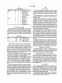


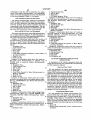


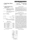


![[v0.3.5.63 Blue Release] (4.17MB PDF)](http://vs1.manualzilla.com/store/data/005758602_1-69f3b29a9a050ef0b6d8d37fccf12e09-150x150.png)