1
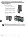
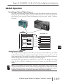
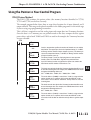
F0-4AD2DA-1 4-CH.
IN/2-CH. OUT ANALOG
CURRENT COMBINATION
CHAPTER
11
In This Chapter...
Module Specifications . . . . . . . . . . . . . . . . . . . . . . . . . . . . . . . . . . . . . . . . . . . . . . .11–2
Setting the Module Jumper . . . . . . . . . . . . . . . . . . . . . . . . . . . . . . . . . . . . . . . . . .11–4
Connecting and Disconnecting the Field Wiring . . . . . . . . . . . . . . . . . . . . . . . . . .11–5
Wiring Diagram . . . . . . . . . . . . . . . . . . . . . . . . . . . . . . . . . . . . . . . . . . . . . . . . . . . .11–6
Module Operation . . . . . . . . . . . . . . . . . . . . . . . . . . . . . . . . . . . . . . . . . . . . . . . . . .11–7
Special V-memory Locations . . . . . . . . . . . . . . . . . . . . . . . . . . . . . . . . . . . . . . . . . .11–8
Using the Pointer in Your Control Program . . . . . . . . . . . . . . . . . . . . . . . . . . . .11–11
Scale Conversions . . . . . . . . . . . . . . . . . . . . . . . . . . . . . . . . . . . . . . . . . . . . . . . . .11–13
Module Resolution . . . . . . . . . . . . . . . . . . . . . . . . . . . . . . . . . . . . . . . . . . . . . . . .11–16
Analog Input Ladder Logic Filter . . . . . . . . . . . . . . . . . . . . . . . . . . . . . . . . . . . . .11–17
Chapter 11: F0-4AD2DA-1 4-Ch. In/2-Ch. Out Analog Current Combination
1
2
3
4
5
6
7
8
9
10
11
12
13
14
A
B
C
D
Module Specifications
11–2
The F0-4AD2DA-1 Analog Combination
module offers the following features:
• The analog input and output channels are
updated in one scan.
• The removable terminal block makes it possible
to remove the module without disconnecting the
field wiring.
• Analog inputs can be used as process variables for
the four (4) PID loops in the DL05 and the eight
(8) PID loops in the DL06 CPUs.
• On-board active analog filtering and RISC-like
microcontroller provide digital signal processing
to maintain precise analog measurements in noisy
environments.
R
PW
N
RU
U
CP
TX1
1
RX
TX2
2
RX
NOTE: The DL05 CPU’s analog feature for this module requires DirectSOFT32 Version 3.0c (or later) and
firmware version 3.30 (or later). The DL06 requires DirectSOFT32 version V4.0, build 16 (or later) and
firmware version 1.00 (or later). See our website for more information: www.automationdirect.com.
DL05/06 Option Modules User Manual; 7th Ed. Rev. A, 08/11
Chapter 11: F0-4AD2DA-1 4-Ch. In/2-Ch. Out Analog Current Combination
The following tables provide the specifications for the F0–4AD2DA–1 Analog Combination
Module. Review these specifications to make sure the module meets your application
requirements.
Input Specifications
Number of Channels
Input Range
Resolution
Step Response
Crosstalk
Active Low-pass Filtering
Input Impedance
Absolute Maximum Ratings
Converter type
Linearity Error (End to End)
Input Stability
Full Scale Calibration Error
(Offset error not included)
Offset Calibration Error
4, single ended (one common)
0 to 20 mA or 4 to 20 mA (jumper selectable)
12 bit (1 in 4096) for 0-20mA, scaled for 4-20mA
25.0 ms (typ) to 95% of full step change
-80 dB, 1/2 count maximum *
-3 dB at 40Hz (-12 dB per octave)
125 Ohm _0.1%, 1/8 W current input
-30 mA to +30 mA current input
Successive approximation
±2 counts
± 1 count *
± 10 counts maximum @ 20mA current input*
± 5 counts maximum @ 0mA current input *
±.4% @ 25°C (77°F)
Maximum Inaccuracy
±.85% 0 to 60°C (32 to 140°F)
±100 ppm typical full scale calibration
Accuracy vs. Temperature
(including maximum offset change)
Recommended Fuse (external)
0.032 A Series 217 fast-acting, current inputs
*One count in the specification table is equal to one least significant bit of the analog data value (1 in 4096).
Output Specifications
Number of Channels
Output Range
Output Type
Resolution
Maximum Loop Voltage
Load (ohms)/Loop Power Supply
Linearity Error (end to end)
Conversion Settling Time
Full Scale Calibration Error
Note: Error depends on the load from
source terminal to ground.
2, single ended (one common)
4 to 20 mA or 0 to 20 mA (jumper selectable)
Current sourcing
12 bit (1 in 4096) for 0 to 20 mA, scaled for 4 to 20 mA
30 VDC
0-300/18-30V
± 2 counts (± 0.050% of full scale) maximum *
400µS max. full scale change
± 26 counts max. @ 300⏲ load
± 18 counts max. @ 250⏲ load
± 12 counts max. @ 125⏲ load
± 10 counts max. @ 300⏲ load
± 8 counts max @ 250⏲ load
Offset Calibration Error
± 6 counts max. @ 125⏲ load
300⏲ load 0.4% @ 60°C
Max. Full Scale Inaccuracy
250⏲ load 0 3%@60°C
(% of full scale) all errors included
125⏲ load 0.2% @ 60°C
* One count in the specification tables is equal to one least significant bit of the analog data value (1 in 4096).
DL05/06 Option Modules User Manual; 7th Ed. Rev. A, 08/11
1
2
3
4
5
6
7
8
9
10
11
12
13
14
A
B
C
D
11–3
Chapter 11: F0-4AD2DA-1 4-Ch. In/2-Ch. Out Analog Current Combination
General Specifications
1
2
3
4
5
6
7
the Module Jumper
8 SettingThe
position of the J2 jumper determines the input and output signal level. You can choose
between 0–20mA and 4–20mA signal levels. The module ships without the jumper connecting
9
the pins (pins not jumpered). In this position, the input and output signal level is 4–20mA. To
select 0–20mA signal level, install the jumper, connecting the pins.
10
11
12
The J2 jumper is shown in the 4–20mA
position (not installed). Install the jumper
13
for the 0–20mA position.
14
A
WARNING: Before removing the analog module or the terminal block on the face of the module,
B
disconnect power to the PLC and all field devices. Failure to disconnect power can result in damage to
the PLC and/or field devices.
C
D
PLC Update Rate
4 input channels per scan, 2 output channels per scan
16-bit Data Word
12 binary data bits
Operating Temperature
0 to 60°C (32 to 140°F)
Storage Temperature
-20 to 70°C (-4 to 158°F)
Relative Humidity
5 to 95% (non-condensing)
Environmental Air
No corrosive gases permitted
Vibration
MIL STD 810C 514.2
Shock
MIL STD 810C 516.2
Noise Immunity
NEMA ICS3-304
Power Budget Requirement
100 mA @ 5VDC (supplied by base)
Connector
Phoenix Mecano, Inc., Part No. AK1550/8-3.5 - green
Connector Wire Size
28 - 16 AWG
Connector Screw Torque
0.4 Nm
Connector Screwdriver Size
DN-SS1 (recommended)
J2
C14
11–4
DL05/06 Option Modules User Manual; 7th Ed. Rev. A, 08/11
Chapter 11: F0-4AD2DA-1 4-Ch. In/2-Ch. Out Analog Current Combination
Connecting and Disconnecting the Field Wiring
Wiring Guidelines
Your company may have guidelines for wiring and cable installation. If so, you should check
those before you begin the installation. Here are some general things to consider:
• Use the shortest wiring route whenever possible.
• Use shielded wiring and ground the shield at the transmitter source. Do not ground the shield at both
the module and the source.
• Do not run the signal wiring next to large motors, high current switches, or transformers. This may
cause noise problems.
• Route the wiring through an approved cable housing to minimize the risk of accidental damage.
Check local and national codes to choose the correct method for your application.
A separate transmitter power supply may be required, depending on the type of transmitter
being used.
This module has a removable connector to make wiring and module removal easier. To remove
the terminal block, disconnect power to the PLC and the field devices. Pull the terminal block
firmly until the connector separates from the module.
The analog module can be removed from the PLC by folding out the retaining tabs at the top
and bottom of the module. As the retaining tabs pivot upward and outward, the module’s
connector is lifted out of the PLC socket. Once the connector is free, you can lift the module
out of its slot.
DL05/06 Option Modules User Manual; 7th Ed. Rev. A, 08/11
1
2
3
4
5
6
7
8
9
10
11
12
13
14
A
B
C
D
11–5
Chapter 11: F0-4AD2DA-1 4-Ch. In/2-Ch. Out Analog Current Combination
Use the following diagram to connect the field wiring. If necessary, the terminal block can be
removed to make removal of the module possible without disturbing field wiring.
Typical User Wiring
Internal
Module
Wiring
See NOTE 1
–
CH1
2–wire
Current
Transmitter
CH2
2–wire
Current
Transmitter
–
CH3
4–wire
Current
+
Transmitter
+
A n a l o g In/Out
4–In/2–Out
0–20mA
4–20mA
IN
–
1
+
2
125Ω
3
125Ω
4
125Ω
0V
125Ω
Analog Switch
1
2
3
4
5
6
7
8
9
10
11
12
13
14
A
B
C
D
Wiring Diagram
+
–
+
CH4
3–wire
+
Current
–
Transmitter
IN
A to D
Converter
1
2
3
4
0V
1
CH 1 load
300Ω
maximum
resistance
D to A
Converter
1
D to A
Converter
+V
2
2
CH 2 load
24V
300Ω
OUT
F0–4AD2DA–1
maximum
resistance
OUT
–
NOTE 1: Shields should be grounded at the signal
source.
NOTE 2: Connect all external power supply
commons.
+
OV
Transmitter
Power Supply
Current Loop Transmitter Impedance
Manufacturers of transmitters and transducers specify a wide variety of power sources for their
products. Follow the manufacturer’s recommendations.
In some cases, manufacturers specify a minimum loop or load resistance that must be used with
the transmitter. The F0-04AD2DA-1 provides 125 ohm resistance for each channel. If your
transmitter requires a load resistance below 125 ohms, you do not have to make any changes.
However, if your transmitter requires a load resistance higher than 125 ohms, you need to add
a resistor in series with the module.
Consider the following example for a transmitter being operated from a 30 VDC supply with
a recommended load resistance of 750 ohms. Since the module has a 125 ohm resistor, you need
to add an additional resistor.
R = Tr – Mr
R = resistor to add
R = 750 – 125
Tr = Transmitter Requirement
R 욷 625
Mr = Module resistance (internal 125 ohms)
Two-wire Transmitter
+
–
DC Supply
+30V
0V
Module Channel 1
R
CH1
COM
125 ohms
0V
11–6
DL05/06 Option Modules User Manual; 7th Ed. Rev. A, 08/11
Chapter 11: F0-4AD2DA-1 4-Ch. In/2-Ch. Out Analog Current Combination
Module Operation
Input/Output Channel Update Sequence
The DL05 and DL06 will read four channels of input data and two channels of output data
during each scan. Each CPU supports special V-memory locations that are used to manage the
data transfer. This is discussed in more detail beginning on the next page, “Special V–memory
Locations”.
Scan
DL05/DL06 PLC
Read Inputs
Execute Application Program
Read the data
Store data
Scan N
Ch 1, 2, 3, 4 IN; Ch 1,2 OUT
Scan N+1
Ch 1, 2, 3, 4 IN; Ch 1,2 OUT
Scan N+2
Ch 1, 2, 3, 4 IN; Ch 1,2 OUT
Scan N+3
Ch 1, 2, 3, 4 IN; Ch 1,2 OUT
Scan N+4
Ch 1, 2, 3, 4 IN; Ch 1,2 OUT
Write to Outputs
Analog Module Updates
Even though the channel updates to the CPU are synchronous with the CPU scan, the module
asynchronously monitors the analog transmitter signals and converts each signal into a 12-bit
binary representation. This enables the module to continuously provide accurate measurements
without slowing down the discrete control logic in the RLL program.
The module takes approximately 25 milliseconds to sense 95% of the change in the analog
signal. For the vast majority of applications, the process changes are much slower than these
updates.
NOTE: If you are comparing other manufacturers’ update times (step responses) with ours, please be aware
that some manufacturers refer to the time it takes to convert the analog signal to a digital value. Our analog
to digital conversion takes only a few microseconds. It is the settling time of the filter that is critical in
determining the full update time. Our update time specification includes the filter settling time.
DL05/06 Option Modules User Manual; 7th Ed. Rev. A, 08/11
1
2
3
4
5
6
7
8
9
10
11
12
13
14
A
B
C
D
11–7
Chapter 11: F0-4AD2DA-1 4-Ch. In/2-Ch. Out Analog Current Combination
1
2
3
4
5
6
7
8
9
10
11
12
13
14
A
B
C
D
Special V-memory Locations
11–8
Formatting theModule Data
The DL05 and DL06 PLCs have three special V-memory locations assigned to their respective
option slots. These V-memory locations allow you to:
• specify the data format (binary or BCD)
• specify the number of input and output channels to scan.
• specify the V-memory locations to store the input data
• specify the V-memory locations to store the output data
DL05 Data Formatting
The table below shows the special V-memory locations used by the DL05 PLC for the analog
combination module.
Analog Combination Module
DL05 Special V-memory Locations
Data Type and Number of I/O Channels
Input Storage Pointer
Output Storage Pointer
V7700
V7701
V7702
Structure of V7700
V–memory location 7700 is used for identifying the number of output channels, the number
of input channels and the data type (binary or BCD). The low byte equals the number of output
channels and the high byte equals the number of input channels. Enter a 1 through 4 to select
the number of input channels and a 1 through 2 to select the number of output channels to be
used. A zero (0) entered for channel selection will cause the channel, either input or output, to
be inoperative.
Loading a constant of 402 into V7700 identifies
MSB
LSB
four input and two output analog channels, and
LOW BYTE
sets the I/O data type to BCD.
Loading a constant of 8482 into V7700 identifies
MSB
LSB
four input and two output analog channels, and
sets the I/O data type to binary.
HIGH BYTE
Structure of V7701
V7701 is a system parameter that points to a V-memory location used for storing analog input
data. The V–memory location loaded in V7701 is an octal number identifying the first Vmemory location for the analog input data. This V–memory location is user selectable. For
example, loading O2000 causes the pointer to write Ch 1’s data value to V2000, Ch 2’s data
value to V2001, CH 3’s data value to V2002 and Ch 4’s data value to V2003.
DL05/06 Option Modules User Manual; 7th Ed. Rev. A, 08/11
Chapter 11: F0-4AD2DA-1 4-Ch. In/2-Ch. Out Analog Current Combination
Structure of V7702
V7702 is a system parameter that points to a V-memory location used for storing analog output
data. The V–memory location loaded in V7702 is an octal number identifying the first Vmemory location for the analog output data. This V–memory location is user selectable. For
example, loading O2010 causes the pointer to read Ch 1’s data value at V2010 and Ch 2’s data
value at V2011.
You will find an example program that loads appropriate values to V7700, V7701and V7702
on page 11–11.
DL05/06 Option Modules User Manual; 7th Ed. Rev. A, 08/11
1
2
3
4
5
6
7
8
9
10
11
12
13
14
A
B
C
D
11–9
Chapter 11: F0-4AD2DA-1 4-Ch. In/2-Ch. Out Analog Current Combination
DL06 Data Formatting
1
2
3
4
5
6
7
8
9
10
11
12
13
14
A
B
C
D
Special V-memory locations are assigned to the four option module slots of the DL06 PLC. The
table below shows these V–memory locations which can be used by the F0–4AD2DA–1.
Analog Combination Module
DL06 Special V-memory Locations
Slot No.
Data Type and Number of Channels
Input Storage Pointer
Output Storage Pointer
1
V700
V701
V702
2
V710
V711
V712
3
V720
V721
V722
4
V730
V731
V732
Setup Data Type and Number of Channels
V–memory locations 700, 710, 720 and 730 are used to set the number of output channels, the
number of input channels and the data type (binary or BCD). The low byte equals the number
of output channels and the high byte equals the number of input channels. Enter a 1 through
4 to select the number of input channels and a 1 through 2 to select the number of output
channels to be used. A zero (0) entered for channel selection will cause the channel, either input
or output, to be inoperative.
Consider the F0–4AD2DA–1 to be installed in
MSB
LSB
slot 2 . Loading a constant of 402 into V710
identifies four input and two output analog
LOW BYTE
channels, and sets the I/O data type to BCD.
MSB
LSB
Loading a constant of 8482 into V710 identifies
four input and two output analog channels, and
HIGH BYTE
sets the I/O data type to binary.
Input Storage Pointer Setup
V–memory locations 701, 711, 721 and 731 are special locations used as a storage pointer for
the analog input data. With the analog module installed in slot 2, the V–memory location
loaded in V711 is an octal number identifying the first user V-memory location to write the
analog input data to. This V–memory location is userselectable. For example, loading O2000
causes the pointer to write Ch 1’s data value to V2000, Ch 2’s data value to V2001, CH 3’s data
value to V2002 and Ch 4’s data value to V2003.
Output Storage Pointer Setup
11–10
V–memory locations 702, 712, 722 and 732 are special locations used as a storage pointer for
the analog output data. With the analog module installed in slot 2, the V–memory location
loaded in V712 is an octal number identifying the first user V-memory location to read the
analog output data from. This V–memory location is user selectable. For example, loading
O2010 causes the pointer to read Ch 1’s data value at V2010 and Ch 2’s data value at V2011.
You will find an example program that loads appropriate values to V710, V711 and V712 on
page 11–12.
DL05/06 Option Modules User Manual; 7th Ed. Rev. A, 08/11
Chapter 11: F0-4AD2DA-1 4-Ch. In/2-Ch. Out Analog Current Combination
Using the Pointer in Your Control Program
DL05 Pointer Method
The DL05 CPU examines the pointer values (the memory locations identified in V7700,
V7701 and V7702) on the first scan only.
The example program below shows how to setup these locations for 4 input channels and 2
output cahneels. This rung can be placed anywhere in the ladder program or in the initial stage
if you are using stage programming instructions.
This is all that is required to read the analog input and output data into V-memory locations.
Once the data is in V-memory you can perform math on the data, compare the data against
preset values, and so forth. V2000 and V2010 are used in the example, the V-memory locations
are user selectable.
SP0
LD
K402
- or LD
K8482
Loads a constant that specifies the number of channels to scan and the
data format. The upper byte selects the input data format (i.e. 0=BCD,
8=Binary) and the number of input channels (set to 4). The lower byte
selects the output data format (i.e. 0=BCD, 8=Binary) and the number
of output channels (set to 2).
The binary format is used for displaying data on some operator
interface units. The DL05 PLCs support binary math functions.
OUT
V7700
Special V-memory location assigned to the option slot contains the
data format and the number of channels to scan.
LDA
O2000
This loads an octal value for the first V-memory location that will be used
to store the incoming data. For example, the O2000 entered here would
designate the following addresses:
Ch1 – V2000, Ch2 – V2001, Ch3 – V2002, Ch4 – V2003
OUT
V7701
The octal address (O2000) is stored here. V7701 is assigned to the
option slot and acts as a pointer, which means the CPU will use the
octal value in this location to determine exactly where to store the
incoming data.
LDA
O2010
This loads an octal value for the first V-memory location that will be used
to store the output data. For example, the O2010 entered here would
designate the following addresses:
Ch1 – V2010, Ch2 – V2011
OUT
V7702
The octal address (O2010) is stored here. V7702 is assigned to the
option slot and acts as a pointer, which means the CPU will use the
octal value in this location to determine exactly where to get the output
data.
DL05/06 Option Modules User Manual; 7th Ed. Rev. A, 08/11
1
2
3
4
5
6
7
8
9
10
11
12
13
14
A
B
C
D
11–11
Chapter 11: F0-4AD2DA-1 4-Ch. In/2-Ch. Out Analog Current Combination
DL06 Pointer Method
1
2
3
4
5
6
7
8
9
10
11
12
13
14
A
B
C
D
11–12
Use the special V–memory table as a guide to setup the pointer values in the following example
for the DL06. Slot 1 is the left most option slot. The CPU will examine the pointer values at
these locations only after a mode transition, first scan only.
Analog Combination Module
DL06 Special V-memory Locations
Slot No.
No. of Channels
Input Pointer
Output Pointer
1
V700
V701
V702
2
V710
V711
V712
3
V720
V721
V722
4
V730
V731
V732
The F0–4AD2DA–1 can be installed in any available DL06 option slot. Using the example
program from the previous page, but changing the V–memory addresses, the ladder diagram
below shows how to setup these locations for 4 input channels and 2 output channels with the
module installed in slot 2 of the DL06. Use the above table to determine the pointer values if
locating the module in any of the other slot locations. Place this rung anywhere in the ladder
program or in the initial stage if you are using stage programming instructions.
Like the DL05 example, this logic is all that is required to read the analog input data into Vmemory locations. Once the data is in V-memory you can perform mathmatical calculations
with the data, compare the data against preset values, and so forth. V2000 and V2010 is used
in the example but you can use any user V-memory location.
SP0
LD
K402
- or LD
K8482
OUT
V710
LDA
O2000
OUT
V711
LDA
O2010
OUT
V712
Loads a constant that specifies the number of channels to scan and the
data format. The upper byte selects the input data format (i.e. 0=BCD,
8=Binary) and the number of input channels (set to 4). The lower byte
selects the output data format (i.e. 0=BCD, 8=Binary) and the number
of output channels (set to 2).
The binary format can be used for displaying data on some
operator interface units and on the DL06 LCD display. The DL06
PLCs support binary math functions.
Special V-memory location, V710, assigned to the option slot
contains the data format and the number of channels to scan.
This loads an octal value for the first V-memory location that will be used
to store the incoming data. For example, the O2000 entered here would
designate the following addresses:
Ch1 – V2000, Ch2 – V2001, Ch3 – V2002, Ch4 – V2003
The octal address (O2000) is stored here. V711 is assigned to the
option slot and acts as a pointer, which means the CPU will use the
octal value in this location to determine exactly where to store the
incoming data.
This loads an octal value for the first V-memory location that will be used
to store the output data. For example, the O2010 entered here would
designate the following addresses:
Ch1 – V2010, Ch2 – V2011
The octal address (O2010) is stored here. V712 is assigned to the
option slot and acts as a pointer, which means the CPU will use the
octal value in this location to determine exactly where to get the output
data.
DL05/06 Option Modules User Manual; 7th Ed. Rev. A, 08/11
Chapter 11: F0-4AD2DA-1 4-Ch. In/2-Ch. Out Analog Current Combination
Scale Conversions
Scaling the Input Data
Many applications call for measurements in
engineering units, which can be more meaningful
than raw data. Convert to engineering units using
the formula shown to the right.
You may have to make adjustments to the formula
depending on the scale you choose for the
engineering units.
Units = A H – L + L
4095
H = High limit of the engineering
unit range
L = Low limit of the engineering
unit range
A = Analog value (0 – 4095)
For example, if you wanted to measure pressure (PSI) from 0.0 to 100.0 then you would have
to multiply the analog value by 10 in order to imply a decimal place when you view the value
with the programming software or a handheld programmer. Notice how the calculations differ
when you use the multiplier.
Analog Value of 2024, slightly less than half scale, should yield 49.4 PSI
Example without multiplier
Example with multiplier
Units = A H – L + L
4095
Units = 10 A H – L + L
4095
Units = 2024 100 – 0 + 0
4095
Units = 20240 100 – 0 + 0
4095
Units = 49
Units = 494
DL05/06 Option Modules User Manual; 7th Ed. Rev. A, 08/11
1
2
3
4
5
6
7
8
9
10
11
12
13
14
A
B
C
D
11–13
Chapter 11: F0-4AD2DA-1 4-Ch. In/2-Ch. Out Analog Current Combination
The Conversion Program
1
2
3
4
5
6
7
8
9
10
11
12
13
14
A
B
C
D
The following example shows how you would write the program to perform the engineering
unit conversion from input data formats 0–4095. This example assumes the raw input data read
at V2000 is in BCD format.
Note: this example uses SP1, which is always on. You could also use an X, C, etc. permissive
contact.
SP1
LD
V2000
When SP1 is on, load channel 1 data to the accumulator (for
a range of 0–1000).
MUL
K1000
Multiply the accumulator by 1000.
DIV
K4095
Divide the accumulator by 4095 (the module resolution).
OUT
V2100
Store the result in V2100.
Output Conversion Program
The following example program shows how you would write the program to perform the
engineering unit conversion to output data formats 0–4095. This example assumes you have
calculated or loaded the engineering unit values between 0–1000 in BCD format and stored
them in V2300 and V2301 for channels 1 and 2 respectively. Both the DL05 and DL06 offer
instructions that allow you to perform math operations using BCD format. It is usually easier
to perform any math calculations in BCD and then convert the value to binary before you send
the data to the module.
SP1
LD
V2300
MUL
K4095
Multiply the accumulator by 4095.
DIV
K1000
Divide the accumulator by 1000 (this is the maximum value of
V2300).
OUT
V2010
Store the BCD result in V2010; the V–memory location set up to
send the data to Ch 1 output.
SP1
LD
V2301
MUL
K4095
DIV
K1000
OUT
V2011
11–14
The LD instruction loads the engineering units used with channel 1 into
the accumulator. This example assumes the numbers are BCD. Since
SP1 is used, this rung automatically executes on every scan. You could
also use an X, C, etc. permissive contact.
The LD instruction loads the engineering units used with Ch 2 into the
accumulator. This example assumes the numbers are BCD. Since SP1 is
used, this rung automatically executes on every scan. You could also use
an X, C, etc. permissive contact.
Multiply the accumulator by 4095.
Divide the accumulator by 1000 (this is the maximum value of
V2301).
Store the BCD result in V2011; the V–memory location set up to send
the data to Ch 2 output.
DL05/06 Option Modules User Manual; 7th Ed. Rev. A, 08/11
Chapter 11: F0-4AD2DA-1 4-Ch. In/2-Ch. Out Analog Current Combination
Analog and Digital Value Conversions
Sometimes it is useful to convert between the signal levels and the digital values. This is
especially helpful during machine startup or troubleshooting. The following tables provide
formulas to make this conversion easier.
Range
4 to 20mA
If you know the digital value
A = 16D + 4
4095
For example, if you have measured the signal as 10mA,
you can use the formula to determine the digital value
(D) that will be stored in the V-memory location that
contains the data.
Range
0 to 20mA
If you know the digital value
A = 20D
4095
If you know the analog signal level
D = 4095 (A - 4)
16
D = 4095 (A – 4)
16
4095
(10mA – 4)
D=
16
D = (255.93) (6)
D = 1536
If you know the analog signal level
D = 4095 (A)
20
4095
This example shows the result for the 0 to 20mA range. D = 20 (A)
D = 4095 (10mA)
20
D = (204.75) (10)
D = 2047.5
DL05/06 Option Modules User Manual; 7th Ed. Rev. A, 08/11
1
2
3
4
5
6
7
8
9
10
11
12
13
14
A
B
C
D
11–15
Chapter 11: F0-4AD2DA-1 4-Ch. In/2-Ch. Out Analog Current Combination
1
2
3
4
5
6
7
8
9
10
11
12
13
14
A
B
C
D
Module Resolution
Analog Data Bits
The first twelve bits represent the analog data in binary format.
MSB
Bit
0
1
2
3
4
5
Value
1
2
4
8
16
32
Bit
6
7
8
9
10
11
Value
64
128
256
512
1024
2048
LSB
1 1 9 8 7 6 5 4 3 2 1 0
1 0
= data bits
Resolution Details
11–16
Since the module has 12-bit resolution, the analog signal is converted from 4096 counts ranging
from 0–4095 (212). For example, a 4mA signal would be 0 and 20mA signal would be 4095.
This is equivalent to a binary value of 0000 0000 0000 to 1111 1111 1111, or 000 to FFF
hexadecimal. The diagrams below show how this relates to the two signal ranges.
4 – 20mA
20mA
Resolution = H – L
4095
H = high limit of the signal range
L = low limit of the signal range
4mA
0 Counts
4095
16mA / 4095 = 3.907μA per count
0 – 20mA
20mA
20mA / 4095 = 4.884μA per count
0mA
0 Counts
4095
DL05/06 Option Modules User Manual; 7th Ed. Rev. A, 08/11
Chapter 11: F0-4AD2DA-1 4-Ch. In/2-Ch. Out Analog Current Combination
Analog Input Ladder Logic Filter
PID Loops / Filtering:
Please refer to the “PID Loop Operation” chapter in the DL06 or DL05 User Manual for
information on the built-in PV filter (DL05/06) and the ladder logic filter (DL06 only) shown
below. A filter must be used to smooth the analog input value when auto tuning PID loops to
prevent giving a false indication of loop characteristics.
Smoothing the Input Signal (DL06 only):
The filter logic can also be used in the same way to smooth the analog input signal to help
stabilize PID loop operation or to stabilize the analog input signal value for use with an operator
interface display, etc.
WARNING: The built-in and logic filters are not intended to smooth or filter noise generated by improper
field device wiring or grounding. Small amounts of electrical noise can cause the input signal to bounce
considerably. Proper field device wiring and grounding must be done before attempting to use the filters
to smooth the analog input signal.
Using Binary Data Format
SP1
LDD
V2000
Loads the analog signal, which is in binary format
and has been loaded from V–memory location
V2000 – 2001, into the accumulator. Contact SP1
is always on.
BTOR
Converts the binary value in the accumulator
to a real number.
SUBR
V1400
Subtracts the real number stored in location
V1400 from the real number in the accumulator,
and stores the result in the accumulator. V1400
is the designated workspace in this example.
MULR
R0.2
Multiplies the real number in the accumulator by
0.2 (the filter factor), and stores the result in the
accumulator. This is the filtered value. The filter
range is 0.1 to 0.9. Smaller filter factors
increase filtering. (1.0 eliminates filtering.)
ADDR
V1400
Adds the real number stored in location V1400
to the real number filtered value in the
accumulator, and stores the result in the accumulator.
OUTD
V1400
Copies the value in the accumulator to
location V1400.
RTOB
Converts the real number in the
accumulator to a binary value, and
stores the result in the accumulator.
OUT
V2100
Loads the binary number filtered value from
the accumulator into location V2100 to use in
your application or PID loop.
DL05/06 Option Modules User Manual; 7th Ed. Rev. A, 08/11
1
2
3
4
5
6
7
8
9
10
11
12
13
14
A
B
C
D
11–17
Chapter 11: F0-4AD2DA-1 4-Ch. In/2-Ch. Out Analog Current Combination
1
2
3
4
5
6
7
8
9
10
11
12
13
14
A
B
C
D
NOTE: Be careful not to do a multiple number conversion on a value. For example, if you are using the pointer
method in BCD format to get the analog value, it must be converted to binary (BIN) as shown below. If you
are using the pointer method in Binary format, the conversion to binary (BIN) instruction is not needed.
SP1
LD
V2000
Loads the analog signal, which is in BCD format
and has been loaded from V–memory location
V2000, into the accumulator. Contact SP1
is always on.
BIN
Converts the BCD value in the accumulator
to binary.
BTOR
Converts the binary value in the accumulator
to a real number.
SUBR
V1400
Subtracts the real number stored in location
V1400 from the real number in the accumulator,
and stores the result in the accumulator. V1400
is the designated workspace in this example.
MULR
R0.2
Multiplies the real number in the accumulator by
0.2 (the filter factor), and stores the result in the
accumulator. This is the filtered value. The filter
range is 0.1 to 0.9. Smaller filter factors
increase filtering. (1.0 eliminates filtering.)
ADDR
V1400
Adds the real number stored in location V1400
to the real number filtered value in the
accumulator, and stores the result in the accumulator.
OUTD
V1400
Copies the value in the accumulator to
location V1400.
RTOB
Converts the real number in the
accumulator to a binary value, and
stores the result in the accumulator.
BCD
Converts the binary value in the accumulator
to a BCD number. Note: The BCD instruction
is not needed to PID loop PV (loop PV is a
binary number).
OUT
V1402
Loads the BCD number filtered value from
the accumulator into location V1402 to use in
your application or PID loop.
Using BCD Data Format
11–18
DL05/06 Option Modules User Manual; 7th Ed. Rev. A, 08/11