1
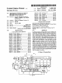
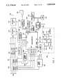
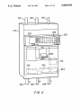
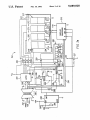
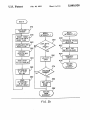
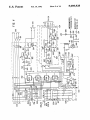
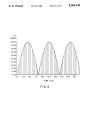
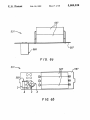
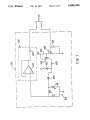
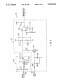
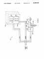
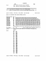
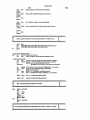
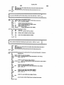
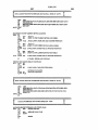
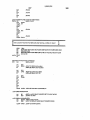
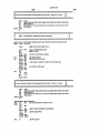
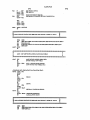
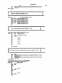
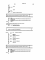
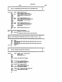
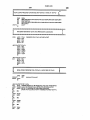
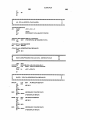
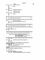
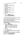
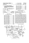
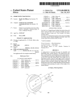
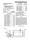
lllllllllllllill|||lllllllllllllllllllllllllllllllllllllllllllllllllllllll
US005089928A
United States Patent [191
[11]
Patent Number:
5,089,928
Durivage, III et a1.
[45]
Date of Patent:
Feb. 18, 1992
[54]
4,706,155 11/1987 Durivage et a1. ................... .. 361/64
4,709,339 11/1987 Femandes ...... ..
364/492
PROCESSOR CONTROLLED CIRCUIT
BREAKER TRIP SYSTEM HAVING
RELIABLE STATUS DISPLAY
[75] Inventors: Leon W. Durivage, III, Marion;
i
_
[73] Assrgnee:
Filed:
Square D Company, Palatlne, 111.
364/483
361/94
364/483
4,794,369 12/1988 Haferd ....... ..
344/166
364/483
2/1989
Andow
4,996,646 2/1991 Farrington
.............. .. 364/483
OTHER PUBLICATIONS
- Aug. 31, 1989
General Electric Publication GEH-4291.
[51]
Int. Cl.5 ............................................. .. H0211 3/04
[52]
us. c1. ...................................... .. 361/94; 361/97;
340/664; 364/433
[58]
. . . . .. 361/96
4,803,635
[21] APp1-N0-= 403,144
[22]
Demeyer . . . . . .
4,783,748 11/1988 Swarztrauber ..
both oflowa
_
1/1988
5/1988 Lagrce et a1.
4,752,853 6/1988 Matsko et a1.
William J, Bacher, Cedar Rapids,
'
4,717,985
4,747,061
Field Of Search .................................. .. 361/93-97;
340/662, 664; 307/66; 364/483
[56]
References Cited
U-S. PATENT DOCUMENTS
4,121,269 10/1978 Hobson ............................... .. 361/44
Schematic of Circuit Board Includin
8
8 Ground Fault '
Test Transducer 5°19 by 59”“ D-
'
Primary Examiner-Todd E. DeBoer
Attorney, Agent, or Firm-Larry I, Golden; Jose w.
Jimenez
[57]
ABSTRACT
A fault-powered, processor-based circuit breaker trip
Pins §ystempmploys a reliable low power trip indicator
4,208,693 6/1980 Dickens et a1.
4,331,997 5/1982 Engel et a1.
361/94
361/93
cucult that is normally powered from the tripping sys
tem. A liquid crystal display is used to indicate the
4,331,998
361/93
status of the system, and a battery is used as a secondary
5/1982 Matsko et a1. .
E1189} cl
,
,
nge
power source after a trip terminates the power to the
et
.
4,335,437 3/1983 Matsko et al. .
.... .. 364/483
4,337,837
3/1983
Matskc et a1. .
.... .. 361/105
4,338,647
6/1982
W1lson et a1. .
...... .. 361/96
-
4,3s1,012 9/1982 E1613 et al. .............. .. 361/96
4,351,013 9/1982 Matsko et a1. .
.......... .. 361/96
4,377,836
3/1983
Elms et a1. . . . .
4,419,619 12/ 1983 Jindrick et a1.
4,428,022 1/ 1934 Engcl 6181 ----- --
1(1);
1
1
-
'
system‘ The- battery ‘5 enabled by a manual switch or "-y
a latch which responds to one of a plurality of trip
.
.
s1gnals
from the processor. The latch also prov1des
.
.
.
.
.
slgnals ‘0 a dnver mm?" 1° dnve the LCD‘ on“ 9“
abled, the battery provldes P0W¢r_t0 th? latch and the
. . . . . . .. 361/96
LCD so that the cause of the mp may be displayed
.... .. 323/257
351/96
during a power fault. The manual switch can be used to
select status signals to be displayed on the LCD, and to
215M211
indicate the condition of the battery. The LCD includes
cm“
t
'd‘
t‘
thtth
‘
i
'
d
d
=61
4,550,360 10/1985 Dougherty ...... ..
4,631,625 12/1986 Alexander et al.
4,680,706 7/1987 Bray .................... ..
4,682,264 7/1987 Demeycr
361/93
361/94
364/492
361/96
p0
t f
. be]
all f It lev l
d . um_
aim“ ° PW“ ‘5
°w
a“
e s a“ m
Clem ‘0 01mm ‘he System
-
4,689,712 7/1987 Dcmeyer ............................. .. 361/96
13 Claims, 10 Drawing Sheets
Vcc
320
322
317
375
1/370 “#371 “T137213”
£2)
DISPLAY
PROCESSOR
US. Patent
Feb. 18, 1992
Sheet 3 of 10
Nwm tnV
Em.
Mm+
?nknpNIEmMk)Pm!
\m
\a
L...
5,089,928
\@18302: 4
o:.PzHm
US. Patent
(
BEGIN
Feb. 18, 1992
Sheet 4 of 10
5,089,928
)
376
INITIALIZE J
MEMORY
BEGIN
378
( INTERRuPT-2 )
RESET TIMER, J
$2105???“
400
K DETERMINE
380
LAST BYTE
STORE DATA AND J
OF
RESET FLAG
PACKET
382
wAIT FOR
YES
FORMAT
SwITcII RELEASE
392
384
VALIDATE J
DATA
SEND DATA
To I_<:D DISPLAY
I
402
?
DgDNvTEggCD J
386
374
DETERMINE J
Y. OF TRIP
RATING
No
388
SEND
DETERMINEDY. To LCD
DISPLAY GRAPH
PHASE
SELECTOR
YES
/
396
SET DATA _/
READY
FLAG
.398
RETURN
FROM
INTERRUPT
FIG. 3b
at
DEBOUNCE
SWITCH
406
US. Patent
Feb. 18, 1992
Sheet 5 of 10
5,089,928
US. Patent
Feb. 18, 1992
Sheet 60f 10
5,089,928
Hf)
(AMPS)
100.00--
/A\.
90.00»
00.00»
/ \
70.00-
/
/_\
// \
\
/
A
\
60.0 . /» \\ /,
332:1"
// \N
\\ /
/
\
\
\ /
10.00
0.00--»
0.0
..
2.5
5.0
7.5
10.0
12.5
TIME (ms)
F165
15.0
17.5
20.0
22.5
US. Patent
Feb. 18, 1992
Sheet 7 of 10
588
F I6. 60
FIG. 6b
5,089,928
US. Patent
Feb. 18, 1992
Sheet 8 of 10
5,089,928
ow?0.?
j Ol |' .
1%
mmw.
Bah
NE\\_I
lIiL
n
n
8%
+
_
_
_
_
|
Rmm1m8
T|_l
mamRm_
“mmmww
m
~
.@
N
US. Patent
Feb. 18, 1992
n@OQ5IP;ES S“.2“:N:9-.
Sheet 9 of 10
5,089,928
US. Patent
Feb. 18, 1992
Sheet 10 of 10
»>
'
5,089,928
0:m9: QdI
vim‘
NSM
\
m+v8Q8M“
W
|\
Mv
IW
Mv
\|6mmmmm
m2
5.4a
A826E. www22
mone
2. :
1
5,089,928
PROCESSOR CONTROLLED CIRCUIT BREAKER
TRIP SYSTEM HAVING RELIABLE STATUS
DISPLAY
TECHNICAL FIELD
The present invention relates generally to circuit
breakers, and, more particularly, to processor con
trolled trip arrangements for circuit breakers.
2
provides power to the LCD driver circuit so that the
cause of the trip may be displayed after a power fault.
Another aspect of the present invention involves an
indication to the user that the fault-powered system is
sensing a low amount of power from the current path.
A segment is employed on the LCD, in response to a
steady state signal representing the power in the current
path, to indicate that a low level of power, below all
fault levels and insuf?cient to power the tripping sys
l0 tem, is in the current path.
BACKGROUND ART
Trip systems are designed to respond to power faults
-
BRIEF DESCRIPTION OF THE DRAWINGS
Other objects and advantages of the invention will
become apparent upon reading the following detailed
description and upon reference to the accompanying
drawings, in which:
detected in circuit breakers. Most simple trip systems
employ an electromagnet to trip the circuit in response
to short circuit or overload faults. The electromagnet .
provides a magnetic ?eld in response to the current
flowing through the breaker. When the current level
FIG. 1 is a block diagram of a microprocessor based '
circuit breaker tripping system, according to the present
increases beyond a predetermined threshold, the mag
netic ?eld “trips” a mechanism which causes a set of 20
circuit breaker contacts to release, thereby “breaking”
the circuit path.
invention;
FIG. 2 is a perspective view of the circuit breaker
tripping system as set forth in the block diagram of FIG.
Many simple trip systems also employ a slower re
FIG. 3a is a diagram illustrating a local display 150 of
sponding bi-metallic strip, which is useful for detecting
FIG. 1;
a more subtle overload fault. This is because the extent
FIG. 3b is a ?ow chart illustrating a manner in which
of the strip’s de?ection represents an accurate thermal
a display processor 316 of FIG. 3a may be programmed
history of the circuit breaker and, therefore, even slight
current overloads. Generally, heat generated by the
to control an LCD display 322 of FIG. 30,‘
FIG. 4 is a schematic diagram illustrating an analog
input circuit 108, a ground fault sensor circuit 110, a
current overload will cause the bi-metallic strip to de~
?ect into the tripping mechanism to break the circuit 30 gain circuit 134 and a power supply 122 of FIG. 1;
path.
FIG. 5 is a timing diagram illustrating the preferred
manner in which signals received from the gain circuit
134 are sampled by the microcomputer 120 of FIG. 1;
The tripping systems discussed above are generally
adequate for many simple circuit breaker applications,
but there has been an increasing demand for a more
intelligent and ?exible tripping system. For example,
many industries today include 3-phase power equip
FIG. 6a is a side view of a rating plug 531 of FIG. 4;
FIG. 6b is a top view of the rating plug 531 of FIG.
35
4;
ment that must be adjusted and monitored on a regular
FIG. 7 is a schematic diagram illustrating a thermal
memory 138 of FIG. 1;
FIG. 8 is a schematic diagram illustrating the reset
circuit 124 of FIG. 1; and
basis. Processor-based tripping systems have been de
veloped to meet these needs.
Processor-based tripping systems typically indicate
the status of the tripping system in an expensive and
FIG. 9 is an illustration of a user select circuit 132 of
power inef?cient manner. One known system, for exam
FIG. 1.
ple, employs a pop-up plunger to indicate certain types
While the invention is susceptible to various modi?
cations and alternative forms, a speci?c embodiment
mechanism that is not only expensive, but also requires 45 thereof has been shown by way of example in the draw
an excessive amount of power.
ings and will herein be described in detail. It shbuld be
Other systems use light emitting diodes (LEDs) to
understood, however, that it is not intended to limit the
of trip causes. The pop-up plunger includes a solenoid
indicate the status of the tripping system. LEDs are less
expensive than the pop-up plunger devices but, due to
their power consumption, require a relatively expensive
50
invention to the particular form disclosed, but on the
contrary, the intention is to cover all modi?cations,
equivalents, and alternatives falling within the spirit and
external power source.
Accordingly, in addition to providing ?exibility to
scope of the invention as de?ned by the appended
claims.
power distribution systems, processor-based tripping
BEST MODES FOR CARRYING OUT THE
systems must also ef?ciently andreliably display their
55
INVENTION
status in a cost effective manner.
System Overview
SUMMARY OF INVENTION
The present invention has direct application for mon
In view of the above,‘a preferred embodiment of the
itoring and interrupting a current path in an electrical
present invention includes a fault-powered, processor
based circuit breaker tripping system having a low 60 distribution system according to speci?cations that may
be programmed by the user. While any type of current
power trip indicator circuit that is normally powered
path would bene?t from the present invention, it is
from the tripping system. An LCD is used to indicate
the status of the system, and a battery is used as a sec
particularly useful for monitoring and interrupting a
three phase current path.
ondary power source after a trip terminates the power
Turning now to the drawings, FIG. 1 shows a block
to the system. The battery is activated by a latch which 65
diagram of an integral microprocessor controlled trip
responds to one of a plurality of trip signals from the
ping system 100 for use with a three-phase current path
processor. The latch also provides signals to a driver
on lines 106 having source inputs 102 and load outputs
circuit to drive the LCD. Once activated, the battery
5,089,928
3
104. The tripping system 100 uses an analog input cir
cuit 108 and a ground fault sensor 110 to detect three
phase current on the current path 106. When the trip
ping system detects an overload, short circuit or ground
4
each ampli?ed signal using its A/D circuitry. By pro
viding two gain stages for each signal A’, B’ and C’, the
microcomputer 120 can immediately perform a high
gain or low gain measurement for each current phase
fault condition, or otherwise determines that the cur
depending on the resolution needed at any given time.
rent path should be interrupted, it engages a solenoid
112 which trips a set of contactors 114 to break the
a reliable power source to the tripping system 100.
current path carrying phases A, B and C. Consequently,
any ground-fault circuit through the earth ground path
or through an optional neutral line (N) is also broken.
The tripping system 100 of FIG. 1 utilizes a number
of circuits to determine when the current path should be
interrupted. This determination is centralized at a mi
The analog input circuit 108 is also utilized to provide
Using current developed from the lines 106, the analog
input circuit 108 operates with a power supply 122 to
provide three power signals (VT, +9 v and +5 v) to
the tripping system 100. The power signal VT is moni
tored by the microcomputer 120 through decoding
circuit 130 to enhance system dependability.
System dependability is further enhanced through the
crocomputer 120, preferably an MC68HC11A1, which
is described in MC68HC11 HCMOS Single Chip Mi 5 use of a thermal memory 138 which the microcomputer
crocomputer'Pragrammer’s Reference Manual, 1985 and
MC68HC11A8 Advance Information HCMOS Single
120 interacts with to simulate a bi-metal deflection
mechanism. The thermal memory 138 provides an accu
Chip Microcomputer, 1985, all being available from Mo
torola, Inc., Schaumburg, Ill. Peripheral circuits that
tem 100 in the event power to the microcomputer 120 is
rate secondary estimate of the heat in the tripping sys
support the microcomputer 120 include a reset circuit 20 interrupted.
The ground fault sensor 110 is used to detect the
124 that veri?es the sanity of the tripping system 100, a
presence of ground faults on one or more of the lines
voltage reference circuit 126 that provides a stable and
106, and to report the faults to the microcomputer 120.
reliable reference for analog to digital (A/D) circuitry
Using user selected trip characteristics, the microcom
located within the microcomputer 120, ROM 128 that
stores the operating instructions for the microcomputer 25 puter 120 determines whether or not the ground fault is
present for a suf?cient time period at a suf?cient level to
120, and a conventional address and data decoding
trip the contactors 114. The microcomputer 120 accu
circuit 130 for interfacing the microcomputer 120 with
mulates the ground fault delay time in its internal RAM.
various circuits including the ROM 128 and a user se
A RAM retention circuit 140 is used to preserve the
lect circuit 132. The address and data decoding circuit
130, for example, includes an address decoder part No. 30 ground fault history for a certain period of time during
power interruptions.
74HCl38, and an eight-bit latch, part No. 74HC373, to
The RAM retention circuit 140 exploits the built-in
latch the lower eight address bits which are alternately
capability of the microcomputer 120 to hold the con
multiplexed with eight data bits in conventional fashion.
tents of its internal RAM provided that an external
The ROM, for example, is part No. 27C64. The user
select circuit 132 allows the user to designate tripping 35 supply voltage is applied to its MOPDB/Vstby input
141. This external supply voltage is stored on a 150
characteristics for the tripping system 100, such as over
microfarad
electrolytic capacitor 143 that is charged
load and phase imbalance fault conditions.
from the +9 volt supply through a 6.2 K ohm resistor
The tripping system 100 is operatively coupled with a
145. The capacitor 143 is charged from the +9 volt
conventional electrical distribution system (not shown)
through input and output restraint circuits 105 and 107. 40 supply, and clamped by diodes to the + 5 volt supply, so
that the capacitor will be rapidly charged during pow
Signals received from the input restraint circuit 105
indicate that a downstream circuit breaker is in an over
load (or over current) condition. The output restraint
circuit 107 is used to send signals to upstream circuit
breakers to indicate the status of its own and all down 45
stream circuit breaker conditions. In general, the trip
ping system 100 will delay tripping of the contactors
er-up.
The ground fault delay time stored in internal RAM
becomes insigni?cant after a power interruption that
lasts longer than about 3.6 seconds. To test whether
such an interruption has occurred, the RAM retention
114 when a downstream breaker is in an overload (or
circuit 140 includes an analog timer 149 having a resis
tor 161 and a capacitor 153 establishing a certain time
this measurement is maintained even in the presence of
non-linear loads.
the user. This information includes the real-time current
and phase measurements on the lines 106, the system
constant, and a Schmitt trigger inverter 155 sensing
over current) condition, assuming that the downstream
circuit breaker opens and clears the condition. Other 50 whether the supply of power to the microcomputer 120
has been interrupted for a time suf?cient for the capaci
wise, the tripping system 100 should not delay tripping
tor 153 to discharge. Shortly after the microcomputer
of the contactors 114. For further detail regarding re
reads the Schmitt trigger 155 during power-up, the
straint-in/restraint-out electrical distribution systems,
capacitor 153 becomes recharged through a diode 157
reference may be made to U.S. Pat. No. 4,706,155 to
55 and a pull-up resistor 159. Preferred component values,
Durivage et a1.
for example, are 365 K ohms for resistor 161, 10 micro
Other circuits are used along with the above circuits
farads for capacitor 153, part No. 74HC14 for Schmitt
to provide reliability and integrity to the trlwping sys
trigger 155, 1N4l48 for diode 157, and 47K ohms for
tem 100. For instance, the microcomputer 120 utilizes
resistor 159.
the analog input circuit 108 along with a gain circuit 134
to measure precisely the RMS (Root Mean Squared) 60 Another important aspect of the tripping system 100
is its ability to transfer information between itself and
current on each phase of the lines 106. The accuracy of
The analog input circuit 108 develops phase signals
A’, B’ and C’ that are representative of the current on
lines 106. The gain circuit 134 ampli?es each phase
signal A’, B’ and C’ through respective dual gain sec
tions, from which the microcomputer 120 measures
con?guration of the tripping system 100 and informa
tion relating to the history of trip causes (reasons why
the microcomputer 120 tripped the contactors 114). As
discussed above, the real-time line measurements are
precisely determined using the analog input circuitry
5
5,089,928
6
an NBC part No. UPD7502 LCD Controller/Driver
which includes a four-bit CMOS microprocessor and a
2k ROM. This NEC part is described in NEC
108 and the gain circuit 134. The system con?guration
of the tripping system 100 and other related information
is readily available from ROM 128 and the user select
UPD750l/02/03 CMOS 4-Bit Single Chip Microproces
circuit 132. The information relating to the history of
trip causes is available from a nonvolatile trip memory
144. Information of this type is displayed for the user
sor User’s Manual, available from NBC, Mountain
View, Calif. Other segments 375 of the LCD display
322 may be controlled by the display processor 316 or
by other means to display various types of status mes
sages.
For example, a push button switch 311 may be uti
lized to test a battery 338. To perform this test, the
either locally at a local display 150 or remotely at a
conventional display terminal 162 via remote interface
160. To communicate with the display terminal 162, the
tripping system utilizes an asynchronous communica
tion interface, internal to the microcomputer 120. Using
the MC68HC11, the serial communications interface
(SCI) may be utilized.
FIG. 2 is a perspective view of the tripping system
battery 338 is connected through a diode 313 to one of
the segments 375 so that when the switch 311 is pressed,
the condition of the battery is indicated. The push-but
100 as utilized in a circuit breaker housing or frame 210.
ton switch 311 preferably resets the latch 320 when the
The lines 106 carrying phase currents A, B and C are
shown passing through line embedded current trans
formers 510, 512 and 514 (in dashed lines) which are
40174 integrated circuit.
switch is depressed. For this purpose the switch 311.
activates a transistor 315. The latch, for example, is a
106, the user reconnects the current path using a circuit
breaker handle 220.
Except for the circuit breaker handle 220, the inter
face between the tripping system 100 and the user is
included at a switch panel 222, an LCD display panel 25
300 and a communication port 224. The switch panel
to control segments 375 such that they identify the
phase current (A, B, C or N) on lines 106 being dis
played on the four seven-segment digits 317. For this
purpose the switch 311 activates a transistor 327 to
invert a signal provided from the battery and to inter
rupt the display processor 316. Each time the display
processor 316 is interrupted, the phase current that is
displayed changes, for example, from phase A to B to C
222 provides access holes 230 to permit the user to
adjust binary coded decimal (BCD) dials (FIG. 8) in the
user select circuit 132. The communication port 224
may be used to transfer information to the display termi
nal 162 via an optic link (not shown).
In the following sections, the tripping system 100 is
further described in detail.
'
Additionally, the switch 311 may be used to select the
20 phase current to be displayed on the LCD display 322
part of the analog input circuit 108. Once the solenoid
112 (also in dashed lines) breaks the current path in lines
.
to ground fault to A, etc.
An optional bar segment 324 is included in the LCD
display 322 to indicate a percentage of the maximum
allowable continuous current in the current path. The
bar segment 324 is controlled by the +5 V signal via a
separate LCD driver 330. The LCD driver 330 operates
A. Local Display
35 in conjunction with the oscillator circuit 328 in the same
manner as the LCD driver 326. However, the LCD
FIG. 3a is a schematic diagram of the local display
driver 330 and the oscillator circuit 328 will function at
150 of FIG. 1. The local display 150 is physically sepa
rated from the remaining portion of the tripping system
a relatively low operating voltage, approximately two
312 include tripping system ground, the +5 V signal
from the power supply 122, serial communication lines
operating power (or current), the LCD driver 330 is
vided by the latch 320 and the display processor 316.
Different segments of the LCD display 322 may be
implemented using a variety of devices including a
display processor 316 to respectively indicate when at
least 20—40%, 40-60%, 60-80% and 80-100% of the
combination static drive/multiplex custom or semi-cus
load.
to three volts. An MCl4070 integrated circuit, available
100, but coupled thereto using a conventional connec
tor assembly 310. The connector assembly 310 carries a 40 from Motorola, Inc., may used to implement the LCD
drivers 330 and 326. Thus, when the tripping system
plurality of communication lines 312 from the mi
fails to provide the display processor 316 with sufficient
crocomputer 120 to the local display 150. These lines
still able to drive the bar segment 324. The LCD driver
314 for a display processor 316, and data lines 318 for a 45 330 drives the bar segment 324 whenever the tripping
system detects that less than about 20% of the rated trip
latch 320. The data lines 318 include four trip indication
current is being carried on lines 106 to the load.
lines (overload, short circuit, ground fault and phase
As an alternative embodiment, the bar segment 324
unbalance) which are clocked into the latch 320 by yet
may be disabled by disconnecting the LCD driver 330.
another one of the lines 318.
An LCD display 322 displays status information pro 50 Additional bar segments 332-335 are driven by the
tom LCD available from Hamlin, Inc., Lake Mills, Wis.
For additional information on custom or semi-custom
displays, reference may be made to a brochure available
from Hamlin, Inc. and entitled Liquid Crystal Display.
The latch 320 controls the segments 370-373 to re
spectively indicate the trip conditions listed above.
Each of these segments 370-373 is controlled by the
latch 320 using an LCD driver circuit 326 and an oscil
rated trip current is being carried on lines 106 to the
.
The oscillator 328 also uses part No. MC1407O in a
standard CMOS oscillator circuit including resistors
329, 336 and a capacitor 331 that have values, for exam
ple, of l megohm, l megohm, and 0.001 microfarads,
respectively.
Even when a power fault causes the system to trip
and interrupt the current on lines 106, the local display
is still able to operate on a limited basis. This sustained
operation is performed using the battery 338 as a sec
lator circuit 328. The corresponding segment 370-373
ondary power source. The battery, for example, is a 3 to
illuminates when the associated output signal from the
65 3.6 volt lithium battery having a projected seventeen
latch 320 is at a logic high level.
year life. The battery 338 supplies power to portions of
The display processor 316 controls four seven-seg
ment digits 317 as an ammeter to display the current in
the lines 106. The display processor 316, for example, is
the local display 150 only when two conditions are
present: (1) the latch 320 has received a trip signal from
5,089,928
7
.
the microcomputer 120 (or the test switch 311 is acti
vated), and (2) the output voltage level of the +5 V
power supply is less than the voltage level from the
battery 338. When the latch 320 latches in any one of
the four trip indication lines from the data lines 318, a
8
received 7 bytes with the most recently received byte
(last byte). If the 8-bit sum and the last byte are differ
ent, ?ow proceeds to block 398. If the 8-bit sum and the
last byte are the same, the display processor sets the
previously referred to data ready ?ag, depicted at block
The diode 344 is forward biased whenever the second
396, and returns from the interrupt, via block 398, to
block 380.
At block 380, the received data is stored in memory
and the data ready flag is reset.
At blocks 382 and 384, the display processor utilizes
condition is also present. Thus, when the output voltage
level of the +5 V power supply is less than the voltage
level from the battery 338, the diode 344 is forward
biased and the battery 338 provides power to the local
display 150. In addition, the diode 344 is forward biased
until a switch 346, activated by a power-up circuit 348,
played at the LCD display 322 is chosen by the operator
using the switch 311 to sequence through each of the
three phase currents and the ground fault current, as
control signal is generated on a latch output line 340.
The control signal turns on an electronic switch 342
which allows the battery 338 to provide power at Vcc
so long as a diode 344 is forward biased.
a conventional conversion technique to convert the
stored data to BCD format for display at the LCD
display 322 of FIG. 3a. The data that is sent and dis
indicated in the data that is received from the mi
crocomputer 120 of FIG. 1.
allows the +5 V signal to provide power at Vcc. The
power-up circuit 348 activates the electronic switch 346
At block 386, the display processor utilizes received
data, including the sensor identi?cation, the rating plug
type and the long-time pickup level, to determine the
only after resetting the display processor 316. The pow
er-up circuit 348, for example, is part No. ICL7665
working in connection with resistors 349, 351, and 353
percentage of rated trip current being carried on lines
106 of FIG. 1. At block 388, the bar segments (324 and
ohrns, respectively.
332-335
of FIG. 3a) are driven by the display processor
Power is provided from Vcc only to the latch 320,
the LCD driver 326, the LCD driver 330, and the oscil 25 in response to this determination. From block 388, flow
returns to block 378.
lator circuit 328. The LCD driver 330 and the oscillator
Blocks 400-406 of FIG. 3b represent a second inter
circuit 328 receive power from either the battery 338 or
rupt
routine which the display processor may be pro
the +5 V power supply output via diodes 350 and 352.
grammed to execute in response to the depression of the
This arrangement minimizes current drain from the
switch 311. At block 400 of this second interrupt rou
battery 338 while allowing the user to view the status of
tine, the display processor determines which phase (or
the tripping system 100 during any power fault situa
' ground fault) current the operator has selected by de
tion.
pressing the switch 311. At blocks 402 and 4-04, the
Power cannot be drawn from the battery 338 unless
display processor monitors its I/O port to determine
the battery 338 is interconnected with the remaining
when the switch 311 is released and to debounce the
35
portion of the tripping system via connector 310, be
signal received from the switch 311. At block 406, the
cause the connector 310 provides the ground connec
display processor executes a return from interrupt com
tion for the negative terminal of the battery 338. This
mand.
aspect of the local display 150 further prolongs battery
It should be noted that the display processor 316 is
life and therefore minimizes system maintenance.
In FIG. 3b, a ?ow chart illustrates the preferred pro 40 optional for the local display 150 and therefore not
having values of 620 K ohms, 300 K ohms and l0 meg
required for its operation. Further, the local display 150
gramming of the display processor 316. The flow chart
is itself an option to the tripping system and is not re
begins at block 376 where the memory internal to the
quired for operating the tripping system.
display processor is initialized. The memory initializa
tion includes clearing internal RAM, input/output ports
and interrupt and stack registers.
At block 378, a software timer is reset and the display
processor waits for a data ready flag which indicates
that data has been received from the microcomputer
120 of FIG. 1. The software timer provides a conven
tional software watchdog function to maintain the san
B. Current and Ground Fault Detection
FIG. 4 illustrates an expanded view of the analog
input circuit 108, the ground fault sensor 110, the power
supply 122 and the gain circuit 134 of FIG. 1. Each of
these circuits receives power from the three-phase cur
50 rent lines 106. Using this power, these circuits provide
45
signals from which the tripping system 100: (l) deter
ity of the display processor. If the software timer is not
mines the phase and current levels on lines 106, (2)
reset periodically (within a certain time interval), the
detects the presence of any ground fault, (3) provides
display processor resets itself.
system power and (4) establishes its current rating.
The data ready flag is set in an interrupt routine,
illustrated by blocks 390 through 398 of FIG. 3b. The 55 (1) Determining Phase and Current Levels
In FIG. 4, the analog input and ground fault sensing
display processor is programmed to execute the inter
circuits 108 and 110 include current transformers 510,
rupt routine when it receives data from the microcom
512 and 514 that are suitably located adjacent the lines
puter 120 of FIG. 1. At block 390 of the interrupt rou
106 for receiving energy from each respective phase
tine, a test is performed to determine if the data byte just
current
path A, B, and C. Each current transformer 510,
received is the last data byte of the packet sent from the
512 and 514 is constructed to produce a current output
microcomputer. If the data byte just received is not the
that is proportional to the primary current in a ?xed
last data byte, flow proceeds to block 398 where a re
ratio. This ratio is set so that when the primary current
turn-from-interrupt instruction is executed. If the data
is 100% of the rated current transformer size (or sensor
byte just received is the last data byte, ?ow proceeds to
65 size), the current transformer is producing a ?xed out
block 392.
put current level. For example, for a 200 Amp circuit
At block 392, a test is performed to determine the
breaker, each current transformer 510, 512 and 514 will
integrity of the received data packet. This is accom
plished by comparing the 8-bit sum of the previously
produce the same current output signal when operating
5,089,928
9
10
at 100% (200 Amps) as a current transformer in a 4000
-continued
Amp circuit breaker which it is operating at 100% (4000
Amps). The preferred construction yields a current
transformer output current of 282.8 milliamperes
(RMS) when the primary current is 100% of the rated
current.
the number of samples;
—
I
(determined by sample rate); and
1(1)
'
sensing toroid 508, full wave recti?er bridges 516, 518
and 520 and the power supply 122 to tripping system
ground. The output currents are returned from tripping
system ground through a burden resistor arrangement
530. The ground fault sensing toroid 508 sums the out
put currents from the transformers 510, 512 and 514. In
a system utilizing a neutral (N) line 106, the ground fault
sensing toroid also sums the output current from a trans
the instantaneous value of the
current ?owing through the breaker.
The output currents provided by the transformers
510, 512 and 514 are routed through a ground fault
time at discrete intervals
The current ?owing through the circuit breaker is
sampled at ?xed time intervals, thereby developing 1(t).
The value of this instantaneous current sample is
squared and summed with other squared samples for a
?xed number of samples N. The mean of this summation
is found by dividing it by N. The ?nal RMS current
value is then found by taking the square root of the
mean.
In FIG. 5, an example of a recti?ed sinusoidal current
former 506, which is coupled to the neutral line (N) to
waveform is illustrated for 1.5 cycles of a 60 hertz signal
sense any return current. A signal representing this
with a peak amplitude of 100 amps. The sampled cur
current summation is produced at an output winding 20 rent is full wave recti?ed. The vertical lines represent
509 and is carried to a fourth recti?er bridge 522. The
the discrete points in time that a value of current is
recti?er bridge 522 is used to detect ground fault condi
sampled. With a sample rate of 0.5 milliseconds, over 25
tions and is discussed in the second part of this section.
milliseconds of time, 50 samples will be taken.
On the right (positive) side of the recti?er bridges
In TABLE 1', the data for the samples from FIG. 4
516-522, positive phase current signals are produced 25 are illustrated in the column labeled l(t) (Amps). The
and added together at lead 524. The current at lead 524
column labeled I(t) SQUARED (Amps) gives the
is used for the power supply 122 which is discussed in
squared values, and the column labeled SUMMATION
(Amps) shows the accumulation of the squared current
the third part of this section.
On the left (negative) side of the recti?er bridges
values over time. The mean of the summation, depicted
516-520, negative phase current signals are carried 30 at the bottom of TABLE 1, is equal to the ?nal accumu
lation divided by the number of samples, or 50. The
through the burden resistor arrangement 530 and trip
square root of this value yields 70.7106854, which is less
ping system ground, and are returned to the recti?er
bridges 516-520 through the power supply 122. This
current path establishes voltage signals A’, B’ and C’,
each referred to as a burden voltage, for measurement
by the microcomputer 120 via the gain circuit 134.
than 0.0000l% in error.
The other columns in TABLE 1 detail the binary
equivalent data that the microcomputer would process
using the ratio that 100 amps equals 255 binary.
The value IRMS will accurately reflect the heating
In FIG. 4, the signals A’, B‘ and C’ are presented to
effect of the current waveform that existed'from t=0 to
the respective dual gain sections for inversion and am
t=N. This current waveform is typically an AC. wave
pli?cation. The gain circuit 134 of FIG. 4 is shown with
one of its three identical dual gain sections, generally 40 form with a fundamental frequency of 50 to 60 Hertz,
but may contain many upper harmonics (i.e., multiples
designated as 533, in expanded form. The dual gain
of the fundamental frequency).
section 533 receives phase signal A’. Each dual gain
section includes a pair of low pass ?lters 532 and a pair
of ampli?ers'534 and 536. The low pass ?lters 532 pro
In practical implementations, several factors affect
the accuracy of the IRMS calculation, including the
vide noise suppression, and the ampli?ers 534 and 536 45 sample rate and the number of samples. In the preferred
embodiment, the sample rate is 2,000 Hertz and atleast
reduce the signal magnitude by 0.5 and increase the
128 samples are taken before the current magnitude is
signal magnitude by a factor of 3, respectively, for the
estimated.
desired resolution. This arrangement allows the mi
(2) Detecting The Presence Of A Ground Fault
crocomputer 120 to instantaneously measure these cur
The
ground fault sensing toroid 508 magnetically
rent levels without wasting time changing any gain
adds the current signals from the input windings 540,
circuitry. Preferred component values are, for example,
542, 544 and 546 to indicate whether or not a ground
10 K ohms for resistors 541, 543, 545, 553 and 555; 4.75
fault is present on lines 106. The toroid 508 is con
K ohms for resistors 547 and 559; 60 K ohms for resistor
structed
with four identical input windings 540, 542, 544
557; and 0.03 microfarads for capacitors 549 and 561.
and 546; one for each of the current transformers 510,
The ampli?ers 551 and 663 are, for example, part No. 55 512 and 514 and one for the neutral current path trans
LMl24.
former 506, which is optional. The toroid 508 has a
Using the gain circuit 134, the microcomputer 120
single output winding 509 which provides a summed
measures the true RMS current levels on lines 106 by
current signal.
sampling the burden voltages developed at signals A’,
The ground fault sensing toroid 508 includes another
B’ and C’. The RMS calculations are based on the for
winding 550 to allow a test signal to be applied at termi
mula:
nals 552. Using momentary switch 554, the test signal
creates a pseudo ground fault for the tripping system.
The tripping system reacts to this pseudo ground fault
z
Imus =
where:
65 in the same manner as a true ground fault. The test
winding 550 is protected by a positive coef?cient resis
tor 556 that increases its resistance as it heats, thereby
limiting the current through it and the winding 550. The
5,089,928
11
12
positive coef?cient resistor is, for example, a Keystone
PTC Resettable Fuse, part No. RL3510-ll0-l20-PTF.
it. Preferred component values are, for example, part
No. 2N6285 for Darlington transistor 568; 1N4739 for
The test winding 550 eliminates the need for a separate
zener diode 570; and 220 ohms for resistor 572.
test transformer which has been utilized by systems in
the prior art.
VT (“trip voltage”) is provided.
The operation of the ground fault sensing toroid 508
is best understood by considering the operation of the
output signal that is provided using a voltage regulator
At the emitter of the transistor 568, the power signal
The +5 v signal is a regulated +5 v power supply
571 (part No. LP295OACZ-5.0) and a capacitor 582
which prevents the output of the regulator 571 from
oscillating. The voltage regulator takes its input from
tripping system with a ground fault and without a
ground fault. In a balanced three phase system without
a ground fault, the current magnitude in each phase is
equal but 120 degrees out of phase with the other pha
ses, and no neutral current exists; thus, the output wind
ing 509 produces no current. As the current through
any phase (A, B or C) increases, the current in the neu
VT via a diode 576. The diode 576 charges capacitor
584 to within one diode drop (0.6 v) of VT and creates
a second supply source of approximately +9 v, which is
referred to as the +9 V power supply. The energy
stored in the capacitor 584 enables the electronic cir
tral path is vectorially equal in magnitude but opposite
in direction to the increase in phase current, and the
magnetic summation is still zero. When a ground fault is
present, current flows through an inadvertent path to an
cuitry being powered by the +9 V power supply to
earth grounded object, by-passing the neutral trans
568, aids in ?ltering voltage ripple. The capacitor 574 is
remain powered for some time after a trip occurs. A
capacitor 574, connected at the emitter of the transistor
former 506 and creating a current signal in the trans 20 also utilized as the energy storage element for the sole
former 509. Thus, the transformer 509 produces a cur
noid 112 which is activated when a power IGFET 583
rent signal only when a ground fault is present.
is turned on by “trip” signals from the microcomputer
The current signal from the output transformer 509 of
(120 in FIG. 1) or from a watchdog circuit (712 in FIG.
the ground fault sensing toroid 508 is routed through
the recti?er bridge 522, the power supply 122 and re
turned through the burden resistor arrangement 530.
8). The trip signals are combined by respective diodes
25 591, 593. The solenoid 112 is also activated by an over
voltage condition sensed by a l6-volt zener diode 595,
The burden resistor arrangement 530 and the recti?er
such as part No. 1N5246. Preferred component values
bridge 522 convert that current signal into an A.C.
are, for example, 220 microfarads for capacitor 574, 100
recti?ed signal 558 that is inverted with respect to trip-v
microfarads for capacitor 584, 10 microfarads for ca
ping system ground, and that has a voltage that is pro 30 pacitor 582, 100 K ohms for resistor 585, 10 K ohms for
portional to the current in the transformer 509.
resistor 589, 0.1 microfarads for capacitor 587, and part
The AC. recti?ed signal 558 is ?ltered by ?lter 560
No. 6660 for IGFET 583.
for noise suppression and then inverted using analog
Diodes 576 and 578 are used to receive current from
invertor 562. From the analog invertor 562, a positive
an optional external power supply (not shown).
going signal is carried to an A/D input at the mi 35 (4) Establishing The Current Rating
crocomputer 120. The microcomputer 120 measures the
On the left side of the recti?er bridges, negative phase
peak levels at the output of the analog invertor 562 to
signals (A’, B’ and C’) from the bridges are provided to
detect the presence of a ground fault. A conventional
the burden resistor arrangement 530, including a rating
voltage divider switch 564 is controlled by the mi
plug 531, to set the current rating for the tripping sys
crocomputer 120 to selectively reduce that signal by
tem. As previously discussed, when the primary current
two thirds, as may be required under severe ground
is 100% of the rated current or “sensor size”, which is
fault conditions. Preferred component values are, for
designated using user select circuit 132, the current
example, 10 K ohms for resistors 565 and 567; 20 K
transformer output current will be 282.8 milliamperes
ohms for resistor 569; 19.6 K ohms for resistor 573; 10 K
ohms for resistor 575; 0.033 microfarads for capacitor 45 (RMS). Thus, when the microcomputer 120 reads the
577; part No. LM124 for ampli?er 579; and part No.
burden voltages using the gain circuit 134 (FIG. 1), the
microcomputer 120 can calculate the actual current in
the lines 106.
(3) Providing System Power
FIG. 4 illustrates parallel connections between re
Power for the'tn'pping system is provided directly
spective
resistors 527 and 529 which are used to estab
50
from the current on lines 106, and current on any one of
lish the maximum allowable continuous current passing
the lines 106 can be used. This feature allows the trip
through the lines 106. The resistors 527 are part of the
ping system to power-up on any one of the three phases
B5170 for IGFET 581.
and to be powered when a ground fault on one or more
of the phase lines 106 is present.
rating plug 531, and the resistors 529 are separatefrom
the rating plug 531. The resistors 529, for example, are
The output currents which are induced by the trans 55 each 4.99 ohm, 1%, 5 watt resistors. This value should
be compared to a corresponding value of 12.4 ohms for
formers 510, 512 and 514 are routed through the recti
?er bridges 516, 518, 520 and 522 to provide the current
for the power supply 122. On the right side of the recti
?er bridges 516-522, at lead 524, the output currents are
summed and fed directly to a Darlington transistor 568,
a 9.1 volts zener diode 570 and a bias resistor 572. Most
of this current ?ows directly through the transistor 568
to ground, to create a constant 9.1 volt level at the base
of the transistor 568. Because it has a nominal emitter to
the burden resistor 525 for the ground fault signal. The
resistors 527 of the rating plug are connected in parallel
with the resistors 529 and hence cause a decrease in the
combined resistance. Therefore, the resistors 529 set the
minimum current rating for the tripping system. In a
preferred arrangement, for example, the minimum cur
rent rating corresponds to 40% of the maximum current
rating. The resistors 527 in the rating plug scale the
base voltage (V eb) of about 1.0 volts, the emitter of the 65 voltages (A’, B’, C’) read by the microcomputer. This
enables the resolution of the A/D converter in the mi
transistor 568 is at approximately 10 volts. The transis
tor 568 will strive to maintain 10 volts across it from
emitter to collector, regardless of the current through
crocomputer to be the same in terms of a fraction of the
rated current for both the minimum and maximum cur
5,089,928
13
rent rating. Consequently, there is not any sacri?ce in
converter resolution for the minimum current rating.
In FIGS. 60 and 6b, the rating plug 531 is shown to
include the resistors 527 mounted on a printed circuit
14
C. Bi-metal De?ection Simulation
The microcomputer 120 is programmed to simulate
accurately the bi-metal deflection mechanism that is
commonly used in processor-less tripping systems. This
is accomplished by accumulating the squared values of
board 587. A connector 588 is used to interconnect the
rating plug with the remaining portion of the tripping
the measured current samples that are sensed by the
analog input circuit 108. The sum of the squared values
of that current is proportional to the accumulated heat
system 100. When the rating plug is absent from the
tripping system, the system reverts to its minimum rat
mg.
in the tripping system 100.
To simulate the bi-metal deflection during cooling,
the microcomputer 120 is programmed to decrement
logarithmically the accumulated square of the current.
The rating plug 531 further includes copper fusible
printed circuit links A, B, C and D which are selectively
disconnected (opened) from a printed circuit connec
tion 589 to inform the microcomputer 120 of the resistor
values, or the burden voltage/current ratio, in the bur
den resistor arrangement 530. The printed circuit con
nection 589 is connected to the +5 V signal via one of
In other words, during a sampling interval, the accumu
lated value A of I(t)2 is decremented by an amount
proportional to A to account for the fact that the rate of
heat loss is proportional to the temperature of the '
the contact points on the connector 588. This connec
power system conductors above ambient temperature.
tion 589 allows the tripping system to encode the
In particular, the temperature in the tripping system 100
printed circuit links A, B, C and D in binary logic such
that one of 16 values of each parallel resistor arrange 20 decreases in response to the current path in lines 106
being broken or intermittent. When this occurs, how
ment is de?ned therefrom. In a preferred arrangement,
ever, the microcomputer 120 loses operating power and
the binary codes “1111” and “1110” are reserved for
therefore can no longer maintain this numerical simula
testing purposes, and the fourteen codes “0000” to
tion.
"1101” correspond to current rating multipliers of 0.400
This problem is overcome by utilizing the thermal
25
to 1.000 as follows:
memory 138 of FIG. 1 to maintain a history of the accu
Code
Current Rating Multiplier
0000
0001
0.400
0.500
0010
0011
0100
0101
0.536
0.583
0.600
0.625
0110
0111
1000
0.667
0.700
0.750
1001
1010
1011
1100
1101
0.800
0.833
0.875
0.900
1.000
The user select circuit 132 of FIG. 9 includes the
mulated current for a predetermined period of time
during which the operating power to the microcom
puter 120 is lost. As illustrated in FIG. 7, this is accom
30 plished using an RC circuit 610 that is monitored and
controlled by the microcomputer 120 to maintain a
voltage on the capacitor 611 that is proportional to the
accumulated square of the current. When the mi
crocomputer loses power, the voltage across the RC
35
circuit 610 logarithmically decays. (The decay is gov
erned by the equation V=V0exp(-t/RC).) Should the
microcomputer power-up again before the voltage
reaches zero, the microcomputer 120 reads the voltage
across the RC circuit 610 using a conventional analog
buffer 612 and initializes its delay accumulator to the
correct value. The analog buffer 612, for example, in
cludes an ampli?er 627 such as part No. LM714 and a
4.7 K ohm resistor 629.
interface circuit used by the microcomputer 120 to read
The preferred RC circuit 610, including a 100 micro
the binary coded resistor value from the rating plug 531.
A tri-state buffer 820 allows the microcomputer 120 to 45 farad capacitor 611 and a 3.24 megohm resistor 613,
provides a ?xed time constant of 324 seconds, or ap
selectively read the logic level of each of the four leads
proximately 5.4 minutes.
representing the status of the four fusible printed circuit
Control over the voltage on the RC circuit 610 is
links on the rating plug 531. A logic high at the input of
provided using IGFET transistors 618 and 620, such as
the buffer 820, provided by the connection between the
fusible printed circuit link and +5 V signal, indicates
that the corresponding link is closed. A logic low at the
input of the buffer 820, provided by pull-down resistors
part Nos. VP0808 and BS170, respectively. During
normal, quiescent conditions, the microcomputer 120
will not be in an overload condition and will drive a
links A, B, C and D may be opened using a current
logic low at the gate of the transistor 620, thereby dis
abling transistors 620 and 622 and allowing the capaci
tor 611 to discharge to tripping system ground. Transis
generator to send an excessive amount of current
tors 618 and 620 work in connection with resistors 621,
826 at the input of the buffer 820, indicates that the
corresponding link is open. The fusible printed circuit
623 and 625, which have values, for example, of 100 K
through the links, thereby causing the copper links to
ohms, 47 K ohms, and 5.1 K ohms, respectively.
burn. This is preferably performed before the rating
During overload conditions, the microcomputer 120
plug 531 is installed in the tripping system. Thus, once
installed, the rating plug 531 automatically informs the 60 accumulates current information in its internal RAM to
microcomputer 120 of its resistor values, and there is no
need to adjust any settings or otherwise inform the
microcomputer of the type of rating plug being used.
simulate the heat level, and drives a logic high at the
gate of the transistor 620 to allow the capacitor 611 to
charge to a selected corresponding level. While the
The microcomputer may adjust the values read from its
capacitor 611 is charging, the microcomputer 120 moni
sponding to the binary coded resistor value to compute
the selected level is reached, the microcomputer drives
actual current values which are independent of the
a logic low at the gate of the transistor 620 to prevent
A/D converter by a predetermined scale factor corre 65 tors the voltage level using the analog buffer 612. When
resistor values in the rating plug 531.
further charging. The voltage on the capacitor 611 is
5,089,928
15
16
against a predetermined threshold value that has been
limited to five volts using a clamping diode 622. The
forward voltage drop across the clamping diode 622 is
balanced by the voltage drop through a series diode
chosen to represent the maximum allowed heat content
of the system. When the accumulated value equals or
exceeds this predetermined threshold value, the trip
ping system will trip the breaker.
A valuable aspect of accumulating the current
squared value is that as the current doubles, the current
squared value quadruples and the internal accumulation
625.
For example, assume that an overload condition sud
denly occurs and the microcomputer 120 has been pro
grammed to allow for a two minute delay before gener
ating a trip signal at this overload fault level. After one
minute in this overload condition, the microcomputer
120 will have accumulated current information which
indicates that it is 50% of the way to tripping. The
register increases at a more rapid rate, resulting in a
more rapid trip. Thus, if the delay time (the period
before the detected power fault causes a trip) is x sec
onds at some current level, as the current doubles, the
microcomputer will also have enabled the RC circuit
610 to charge to 2.5 v; that is, 50% of the maximum 5 v.
delay time will be x/4 seconds.
The formula for calculating the delay time for any
Assuming, for the purpose of this example, that the
overload fault condition is removed at this point and the
electronic trip system loses operating power, when the
power to the microcomputer 120 drops to 0 v, the inter
nally stored current accumulation is lost. However, the
voltage across the RC circuit 610 is still present and will
constant current is:
start to decay by approximately 63.2% every 5.4 min 20
utes (the time constant for the RC circuit 610). There
fore, after 5.4 minutes without current, the voltage
where:
A}; = the accumulation rate in seconds;
across the RC circuit 610 will be 36.8% of 2.5 v, or 0.92
K = predetermined ?nal accumulation value;
v.
If the overload condition would occur again at this 25
point, the microcomputer 120 would power up and
measure 0.92 v across the RC circuit 610. The mi
I=
crocomputer 120 would then initialize its internal cur
rent accumulation to approximately 18% (0.92 v di
vided by the maximum of 5.0 v) of the preprogrammed
full trip delay time.
and
the true RMS value of current ?owing
through the breaker.
30
D. Reset Circuitry
Referring now to FIG. 8, an expanded view of the
The accumulation calculations performed by the
microcomputer are based on the formula:
reset circuit 124 is shown to include a power-up reset
circuit 710 and a watch-dog circuit 712 to maintain the
35
integrity of the tripping system 100. The power-up reset
circuit 710 performs two functions, both of which occur
during power-up: it provides a reset signal (asserted
where:
II
low) on line 743 to maintain the microcomputer 120 in
reset condition untilthe tripping system 100 develops
sufficient operating power from the current lines 106;
and it provides a reset signal (asserted low) via lead 744
the number of samples;
time at discrete intervals
(determined by the accumulation rate); and
1(1)
to the watch-dog circuit 712 to prevent the watch-dog
the true RMS value of current through
the breaker.
45
During a fault, the trip unit will begin to sum the
current squared value as soon as the current exceeds a
predetermined level for a predetermined period of time,
or the selected overload condition. The electronic trip
circuit from engaging the solenoid 112 during power
up. This latter function prevents nuisance tripping.
Preferably the power-up reset circuit includes an
under-voltage sensing integrated circuit 745 that detects
whether or not the output voltage of the + 5 volt supply
is less than a predetermined reference voltage at which
the microcomputer (120 in FIG. 1) may properly func
system will maintain an internal accumulation register 50 tion. The integrated circuit 745 is, for example, part No.
to store a value that is proportional to the square of the
MC33064P-5, which holds the reset line 743 low until
current and that is incremented periodically based on
the output voltage of the +5 volt supply rises above 4.6
the accumulation rate. Assuming a constant fault level
of current, a ?xed accumulation rate, and a known con
volts. The microcomputer 120 may operate at 4.5 volts
dition of the accumulation register at t=0, the value in 55 or above. The preferred reset circuit also includes a
the accumulation register will increase at a determinate
rate and will contain a known value at any giyen time t.
pull-up resistor 741, a capacitor 739, and a diode 753
connecting the integrated circuit 745 to the watchdog
circuit 712. The resistor 741, for example, has a value of
47K ohms and the capacitor 739 has a value of 0.01
sured at 70.71 amperes (RMS) with an accumulation
period of 64 milliseconds. Further assume that the accu— 60 microfarads. The diode 753 ensures that the reset circuit
710 affects the watchdog circuit 712 only when the
mulation register is at zero prior to the fault. The mi
microcomputer 160 is being reset.
crocomputer 120 will accumulate the squared value of
The watch-dog circuit 712 protects the tripping sys
the current every 64 milliseconds into the register, caus
tem
from microcomputer malfunctions. Thus, it is de
ing it to increase at a constant rate.
With a continuous, fixed level fault, as time increases, 65 signed to engage the solenoid 112 if the microcomputer
For'example, assume that a continuous fault is mea
the internal accumulation register increases proportion
ally. In order to protect the system from this fault, this
increasing accumulated value is compared periodically
120 fails to reset the watch-dog circuit 712 within a
predetermined time period. The microcomputer 120
resets the watch-dog circuit 712 by regularly generating
17
5,089,928
logic high pulses, preferably about every 200 millisec
onds, on lead 714. These pulses are passed through a
capacitor 718 to activate an IGFET transistor 720,
which in turn discharges an RC timing circuit 724
through a circuit limiting resistor 733. A resistor 730
and a clamping diode 732 are used to reference the
pulses from the capacitor 718 to ground.
18
G. Communication For Information Display
The microcomputer 120 sends identical tripping sys
tem status information to the local display 150 and the
display terminal 162. The information is sent synchro
nously on a serial peripheral interface 191 to the local
display 150 and asynchronously on a serial communica
tion interface 151 to the display terminal 162. The inter
The pulses on lead 714 prevent the RC timing circuit
faces 151 and 191 may be implemented using the SCI
724 from charging up past a reference voltage, Vref, at
and SP1 ports internal to the MC68HC11. The history
the input of a comparator 726. If the RC timing circuit
of the tripping system status information is stored in the
724 charges up past Vref, the comparator 726 sends a
nonvolatile trip memory 144. That history includes the
trip signal to the solenoid 112 to interrupt the current
speci?c cause and current level of the last trip and a
path in lines 106. The reference voltage, for example, is
running accumulation of the different trip causes.
provided by a 4.3 volt zener diode 427 supplied with 15 The trip memory 144 is preferably an electrically
current througha resistor 729. Preferred component
erasable programmable ROM (EEPROM), for exam
values are, .for example, 0.001 microfarads for capacitor
ple, a X24CO4I, available from Xicor, Inc. of Milpitas, '
718, 27K ohms for resistor 730, part No. 1N4l48 for
Calif. In this case, the serial peripheral interface 191 is‘
diode 732, part No. 138170 for transistor 720, 10 ohms
used for bidirectional data transfer between the mi
for resistor 733, 820K megohms for resistor 737, 0.22 20 crocomputer 120 and the EEPROM 144. This data
microfarads for capacitor 735, part No. LM29031 for
transfer is implemented using one line of the serial pe
comparator 726, part No. 1N4687 for diode 727, 100K
ripheral interface 191 to transfer the data and the other
line to transmit a clock signal between the microcom
ohms for resistor 729, and 10K ohms for resistor 751.
puter 120 and the EEPROM 114 for synchronization.
E. User Select Switches
25 During power up of the tripping system 100, the mi
crocomputer 120 transmits to the trip memory 144 a
As introduced above, the user select circuit 132 is
unique bit pattern which is interpreted as a data request
illustrated in FIG. 9. In addition to the buffer 820 for the
code. The microcomputer 120 then sets the bidirec
rating plug, the user select circuit 132 includes a plural
tional data line as an input and clocks the requested data
ity of user interface circuits 810 each having a pair of
BCD dials 812 and a tri-state buffer 814 which is en 30 in from the trip memory 144.
The microcomputer 120 maintains a copy of the his
abled through the address and data decoder 130 of FIG.
tory data in its internal RAM and in the event of a trip,
1. Each BCD dial 812 allows the user to select one of
updates it and transmits it back into trip memory 144 via
several tripping system characteristics. For example, a,
the interface 191, again utilizing the unique bit pattern
pair of BCD switches may be used to designate the
longtime pickup and the longtime delay (overload trip
ping characteristics) and another pair of BCD switches.
may be used to designate the short time pickup and the
short time delay (short circuit tripping characteristics).
Other BCD switches may be used to designate sensor
and breaker sizes, an instantaneous pickup, ground fault
tripping characteristics, and phase unbalance thresh
olds.
F. Energy Validation For Solenoid Activation
The user select circuit 132 of FIG. 1 and 9 also deter
mines if there is sufficient energy to activate the sole
to set the trip memory 144 to a receive mode. Upon
receipt of the data, trip memory 144 will reprogram its
contents, overwriting the old history information with
the newly received data.
During normal operation (i.e., after power up and
without a trip), the microcomputer 120 transmits opera
tional information over the serial peripheral interface
191. Because this information does not contain the
unique bit patterns required to activate the trip memory
144, the trip memory 144 ignores the normal transmis
45 sions. However, other devices which may be connected
to the serial peripheral interface 191 can receive and
interpret the information correctly.
noid 112. Using the address and data decoding circuit
The microcomputer 120, for example, is programmed
130, the buffer 820 is selected to read one of its input
to execute a communication procedure that permits the
lines 830. The VT signal from the power supply 122 of 50 tripping system 100 to communicate with a relatively
FIG. 1 feeds the input line 830, with the buffer 820
low power processor in the display processor 316. The
being protected from excessive voltage by a resistor 832
procedure utilizes a software interrupt mechanism to
and a clamping diode 834. The resistor 832, for example,
track the frequency with which information is sent on
has a value of 620K ohms.
the interfaces 151 and 191. During normal operation,
Before the microcomputer 120 engages the solenoid 55 one 8-bit byte of information is sent every seven milli
112, the input line 830 is accessed to determine if VT is
seconds. During tripping conditions, information is sent
read as a logic high or a logic low. The buffer 820 pro
continuously as fast as the microcomputer 120 can
vides a logic high at its output whenever the input is
transmit. This procedure allows the display terminal
162 and the display processor 316 to display continu
ously status messages from the tripping system 100
without dedicating their processors exclusively to this
greater than 2.5 v to 3 v. If VT is read as a logic high,
the microcomputer 120 determines that there is suffi
cient power to activate the solenoid 112 and attempts to
do so. If VT is read as a logic low, the microcomputer
120 determines that there is insufficient power to acti
reception function. Equally important, this procedure
permits the microcomputer 120 to perform a variety of
tasks; including continuous analysis of the current on
vate the solenoid 112 and waits, while repeatedly
'
checking VT, in anticipation that an intermittent power 65 lines 106.
Status messages are preferably transmitted using an
fault caused VT to fall. Once VT rises beyond the
8-byte per packet, multi-packet transmission technique.
2.5-3.0 volt level, the microcomputer 120 attempts to
Thetype of information included in each packet may be
activate the solenoid once again.


![[quote(var.text)]}](http://vs1.manualzilla.com/store/data/005937533_1-4dd3fe8a9b5a28fbfb6fbb268c8e3b66-150x150.png)