1
THE
ADVANCED ENERGY®
PE 2500 GENERATOR
User Manual
Option: 100 kl-lz, load matching
PN: 5700248-8
October 1992
THE
ADVANCED ENERGY@
PE 2500 GENERATOR
User Manual
Option: 100 kHz, load matching
ADVANCED ENERGY
INDUSTRIES, INC
1600 Prospect Parkway
Fort Collins, Colorado 80525
(303) 221-4670
Telex #45-0938
PN: 5700248-8
October 1992
To ensure years of dependable service, Advanced Energy. productsare
thoroughly tested and designed to be among the most reliable and highest
quality systems available worldwide. All partsand labor carry our standard
1-year warranty.
For Custom. S.-vIce, call:
AE. Colorado office
(303) 221-0108 (24-hour line)
Fu: (303) 221-5583
AE. California office
(408) 263-8784 (8 a.m. to 5 p.m. Pacific Standard
Time - california only)
Fax: (408) 263-8992
AE. Japanese office
81 (03) 3222-1311
Fu: 81 (03) 3222-1315
AE. German office
49 (0711) 7n-87-18
Fu: 49 (0711) 777-87-00
all others
contact your local service center-see the list on the
next page
©1992, Advanced Energy Industries, Inc
All rights reserved. Printed in the United States of America. This manual is
supplied to enable the reader to safely install, operate, and service the
equipment described herein. Making copiesof any part of this manual for any
purpose other than these is a violation of U.S. copyright law.
In the interest of providing even better equipment, Advanced Energy
Industries, lnc., reserves the right to make product changes wlhout
notification or obligation.
For more information, write Advanced Energy Industries, Inc., 1600 Prospect
Parkway. Fort Collins. CO 80525.
AE Service Centers
Company Name
Phone/Fax Numbers
Vacutec AB
Sweden
46 (0) 40-437270
Fax: 46 (0) 40-435538
Gambetti Kenologia snc
Italy
Fax: 39 (02) 9052778
Segen Technologies, Ltd.
Israel
Fax: 972 (03) 9362030
Zeus Co., Ltd.
Korea
82 (02) 577-3181
Fax: 82 (02) 576-3199
Schmidt Scientific
Taiwan
Fax: 886 (02) 25029692
39 (02) 9055660
972 (03) 93631 06
886 (02) 5013468
Returning Units for Repair
Before returning any product for repair and/or adjustment, call AE Customer
Service and discuss the problem with them. Be prepared to give them the serial
number of the unit and the reason for the proposed return. This consultation
call will allow Customer Service to determine if the unit must actually be
returned for the problem to be corrected. Such technical consultation is always
available at no charge.
If you return a unit without first getting authorization from Customer Service,
and that unit is found to be functional, you will have to pay a retest and
calibration fee, and all shipping charges.
Upgrading Units
AE will upgrade older units for a fee (a percentage of the current list price,
based on the age of the unit. Such an upgraded unit will cany a 6-month
warranty (which will be added to any time remaining on the original warranty).
SAFETY
WARNING
SAFE OPERATING PROCEDURES AND PROPER USE OF THE
EQUIPMENT ARE THE RESPONSIBIUTY OF THE USER OF THIS
SYSTEM.
Advanced Energy Industries, lnc., providesinformation on its productsand
assocated hazards. but it assumes no responsibility for the after-sale
operation of the equipment or the safety practices of the owner or user.
This equipment produces potentially lethal high-voltage, high-current, radio
frequency (RF) energy. You should read this manual and understand Is
contents beforeyou attempt to hook up or operate the equipment it
describes. Folbw all safety precautions. Never defeet Interlocks or
grouncla.
DANGERI All personnel who work with or who
.r. exposed to thll equipment must take
precaution. to protect themselves against
.....ou. or possibly fatal bodily Injury.
DO NOT BE CARELESS AROUND THIS EQUIPMENT.
CONGRATULATIONS
On your purchase of AE's PE generator, designed for hard use in a vacuum
environment. Advanced circuit design and calibrated instrumentation make
these units the most accurate, most efficient, and most versatile in the world
today.
Since 1981, AE's power supplies and controllers have been contributing to a
broad range of advanced technological processes such as semiconductor
fabrication, optical coating, printed circuit manufacturing, glass coating, and
data storage media plating. In the United States, Europe, and Asia,
Advanced Energy Industries, Inc., is known for its quality products and
strong customer support.
CONTENTS
INTRODUCTION
Overview of the Manual . . . . . . . . . . . . . . . . . . . . . . . . . . . i
Interpreting the Manual
ii
PART I GETTING TO KNOW YOUR PE SERIES GENERATOR
1. WHAT IT IS
General Description . . . . . . . . . . . . . . . . . . . . . . . . . . . . . . 1-5
Specifica.tic>ns
1-7
2. HOWIT WORKS
Theory of Operation . . . . . . . . . . . . . . . . . . . . . . . . . . . . .
Front Panel Controls
Status Indicators
Connectors . . . . . . . . . . . . . . . . . . . . . . . . . . . . . . . . . . .
. 2-3
2-7
2-9
. 2-11
PART II OPERATING YOUR PE SERIES GENERATOR
3. PREPARING FOR USE
Setting Up
First-time Operation
3-5
3-9
4. CHOOSING MODES
Remote Control . . . . . . . . . . . . . . . . . . . . . . . . . . . . . . . . . 4-3
PART III SERVICING YOUR PE SERIES GENERATOR
5. CAUBRATION ANDTROUBLESHOOTING
Calibration . . . . . . . . . . . . . . . . . . . . . . . . . . . . . . . . . . . . . 5-5
Troubleshooting
5-7
PART IV LEARNING MORE ABOUT YOUR PE GENERATOR
6. HOOK-UP NOTES
Grounding
Warranty and claims Information
Schematics
6-1
INTRODUCTION
OVERVIEW OF THE MANUAL
The main table of contents is an outline of the major topics covered in the
manual. It shows each chapter and the major sections of each chapter. It
contains only the major sections so that you can skim tt and get a general
idea of what is contained here, without having to look at a lot of headings. In
the manual, the chapter titles and the major sections are printed at the top
right-hand corner of each odd-numbered page.
When you turn to a chapter, you will find a detailed table of contents that
lists each subheading in the chapter. This will show you which page contains
the information you are looking for.
Part 1, Getting to Know Your PE Series Generator, contains two chapters:
What It Is and How It Works. What It Is gives an overview of the PE and a
description of the functional and physical specifications.
How It Works contains a functional block diagram, a description of the
front panel controls and status indicators, and important information on
connectors and signal descriptions.
Part II, Operating Your PE Series Generator, also contains two chapters:
Preparing for Use and Choosing Modes. Preparing for Use provides
information on unpacking, connecting, and starting up your PEe Choosing
Modes tells you how to select remote control.
Part III, Servicing Your PE Series Generator, contains one chapter,
Calibration and Troubleshooting. This chapter tells you how to adjust the PE
and service minor problems.
Part IV, Learning More About Your PE Generator, contains a detailed
description of grounding techniques.
di:-(!)--------------------------
INTERPRETING THE MANUAL
Type Conventions
To help you quickly pick out what is being discussed, the manual presents
certain words and phrases in type that is different from the rest of the text.
Pin and line names appear in capitalized italics (POWCOM). Labels that are
on the PE (switches, indicators, etc.) generally appear in boldface capital
letters (PLASMA). Functions are printed in boldface lowercase letters
(on/off).
ii
PART I
GETTING TO KNOW YOUR
PE SERIES GENERATOR
d2~
PART I
WHAT IT IS
CONTENTS
General Description . . . . . . . . . . . . . . . . . . . . . . . . . . . . . . . . . . . . 1-5
Understanding Switch-mode Operation
Specifications
1-5
1-7
Functional Specifications . . . . . . . . . . . . . . . . . . . . . . . . 1-7
Physical Specifications
1-8
1-3
d2
at
PART I
1-4
WHAT IT IS
GENERAL DESCRIPTION
The PE series power supply is designed as a power source for plasma
processes. The unit delivers power and holds power at the soecfled level
during plasma variations.
You can control the output and monitor the unit either from the front panel
or through an I/O connector provided on the rear panel. PE series units
easily interface with most logic types and both relay and switch contact
closures.
The PE 2500's load-matching network is needed for a wide range of loads.
At a given power level and pressure, plasma operates at a fixed votace
level much like back-to-back zener diodes. Load matching is required when
this voltage is not in the operating range of the power supply.
The PE series uses a resonant power conversion technique coordinated wth
a highly effective line fi~er. This produces extremely efficient operation typical
of switching power supplies while maintaining the low electromagnetic
interference (EMI) of linear power supplies.
Understanding Switch-mode Operation
There are two basic approaches to ac power generation. The first, most
common, is linear operation. The second, more recent development, is
swtch-rnode operation. The following discussion explains the significant
differences between the two types of operation.
Both linear and switch-mode supplies use an input rectfler/tner: however,
linear supplies require a large 60-Hz step up/step down transformer. This
transformer means that linear supplies are larger and heavier than switching
supplies of the same power rating.
Another signnicant difference between linear and switching power supplies of
a given frequency is the control element. Linear supplies use transistors or
tubes as variable resistors that gradually change their value in response to a
control signal. This gradual change causes the supply to dissipate nearly as
much (possibly more) heat as the load. If transistors are used, an addtional
problem called "secondary breakdown" is common. Secondary breakdown
1-5
82
8
PART I
- -- -- -- -- -- -- -- -- -- -- -- -- --
prevents full device use, so large numbers of devices must be combined to
produce the required power.
In contrast, switch-mode supplies use transistors optimized for rapid "turn
on" and "turn off" in series wtth the load. Because each switch is always
either fully on or off, switch-mode supplies dissipate significantly less power
than do linear supplies.
One drawback of using switching supplies with plasma processes is that a
plasma requires a current or "energy" source for proper stabilization. Most
swttching supplies are voltage sources.
The PE series deals with this problem in a unique fashion. First, a reactive
power fitter with a pass characteristic at the fundamental frequency acts as
an energy source, The filter supplies both the voltage and current that the
plasma requires for stability, and in addition, isolates transients (arcs, for
example) from the generator. Because of the smoothing effect of the filter,
the switches can be pulse-width modulated, and power control is attained
with the same devices used for power generation. Hence the description,
pulse-width modulated resonant inverter.
1-6
WHAT IT IS
SPECIFICATIONS
Functional Specifications
Controlling Modes
Local (through the front panel), remote (through
the User I/O port).
Control Signal Sources
Power output can be controlled by internal
analog signals entered from the front panel, or
by external analog signals provided from the
user I/O port.
Power Output
Low frequency output controlled in the constant
power mode.
Interlock Supervision
When connected to a safety switch, the interlock
string disables the unit if a problem occurs.
Status Indicators
LED's on front panel show status of interlocks,
output enable, plasma ignition, and setpoint
level. Remote or local control is also shown.
Fault Conditions
Overtemperature and arc are the conditions that
shut off the output power.
Internal
Load-matching
The load-matching network's voltage transformer
correctly matches the voltage of the power
supply to the voltage of the load.
1-7
PART I
82·--------------------------Physical Specifications
Input Voltage
208 V ac ± 1QOA>
50/60 Hz single phase
Input Current
20 A nominal (full power)
0.72 power factor
25 A circuit breaker
Output Power
1700 W at 550 V nominal output
Output Frequency
100 kHz ± 100 Hz
Ambient Temperature:
Operating
Minimum erc, maximum 400C (maximum value
of average over 24 hr.: 35°C). If the units are
enclosed in cabinets, the operator will ascertain
the temperature at the place of installation and
ensure that the maximum ambient temperature is
not exceeded.
Storage
Minimum -25°C, maximum 55°C.
Transportation
Minimum -25°C, maximum 55°C (for short
periods of up to 24 hrs., the maximum is 70°C).
Coolant Temperature
Air (gas) minimum QOC, maximum 35°C.
Coolant Flow Parameters:
Contamination
Cooling air should be free of corrosive vapors
and particles, conductive particles, and particles
that could become conductive after exposure to
moisture.
Humidity
15-850/0 relative humidity; no condensation or
icing.
Atmospheric Pre88Ure:
Operating
800 mbar minimum (approx. 2000 m above sea
leveO·
1-8
WHAT IT IS
Storage
800 moor minimum (approx. 2000 m above sea
leveQ.
Transportation
660 moor minimum (approx. 3265 m above sea
IeveQ.
1-9
dEe
PART I
1 - 10
HOW IT WORKS
CONTENTS
Theory of Operation . . . . . . . . . . . . . . . . . . . . . . . . . . . . . . . . . ..
Front Panel Controls
Status Indicators
Connectors
2-3
2-7
2-9
2-11
Analog/Digital I/O Connections . . . . . . . . . . . . . . . . . . . 2-11
Signal Descriptions: User I/O Pins
2-13
2-1
2-2
HOW IT WORKS
THEORY OF OPERATION
The PE converts ac line power into rectified dc voltage. The dc vottage
provides an unregulated source for high-frequency inverters. The inverters
convert the unregulated dc voltage to high-frequency ac vottage.
The following sections describe the functional units of the PE power supply.
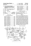
Figure 2-1 on page 2-4 shows the PE block diagram.
Circuit Breaker/EMC Filter
The circuit breaker located on the rear panel automatically protects the
system wiring in the event of a failure. In some units a fuse is used instead
of a circuit breaker. The internal EMC filter reduces the amount of
high-frequency noise conducted to the power lines.
Main Contactor/Rectifier
The main contactor applies incoming ac voltage to the rectifier. The rectifier
converts the ac input to unregulated dc voltage.
Filter/Soft Start
The input fitter reduces EMI conducted at low frequencies. It also reduces
the peak current through the rectifier and the dc fitter capacitor, and
provides a stable input impedance for the dc-to-ac regulator.
The soft start circuit prevents large surge currents when the input power is
turned on. The circuit uses a 50 Q resistor to charge the dc filter capacitor
and then shorts this resistor when the dc filter cap is charged to the normal
operating level.
Auxiliary Power Supply
The auxiliary power supply is a 50/60 Hz transformer with an isolated 40 V
ac center-tapped winding. The secondary winding generates ±24 V dc to
power the control electronics.
Drive Board
The drive board provides isolation between the control logic and the inverter.
2-3
8c·-------------------------PART I
Inverter/Frequency Module/Output Transformer
The inverter chops the dc voltage into a square wave ac voltage that passes
through a series resonant circuit to produce a sine wave. This sine wave
passes through an isoIatbn (output) transformer.
Internal Load Matching Transformer
The transformer's taps allow the PE to efficiently transfer power to a wide
range of loads.
Output Sense
The output sense converts and isolates output volage and current to k:>gic
levels.
Display/User I/O
The display provides status information and control from the front panel. The
user 1/0 port interface provides status and control for the remote interface.
Logic
The bgic provides fault protection, onloff control, and power regulation for
the power supply. Addlional fault protection is provided by the fold-back
current board which plugs into the logic board. The fold-back current
feature monitors output, voltage and current phase and limks output power if
they become excessive, thereby probnging the life of the inverters.
2-4
HOW IT WORKS
Input
Line
Unregulated
300 V de
RF
Output
""--------II1II4
User
I/O
Figure 2-1. PEblock diagram.
2-5
Output
Sense
d2
8
PART I
2-6
HOW IT WORKS
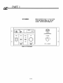
FRONT PANEL CONTROLS
The switches described below provide complete oontrol of the PE power
supply from the front panel. Figure 2-2 on page 2-6 shows the front panel.
POWER ON/OFF
Applies line power to internal circuitry.
OUTPUT ON/OFF
OFF resets the interlocks and
overtemperature fault and removes the output
power. OFF resets in both local and remote
modes. However, in remote mode, power
remains off only as long as the switch is held
off. ON enables power to be transferred to
the output connector. ON works only in local
mode.
LEVEL
Controls output power in local mode.
Rotating the locking skirt clockwise locks the
knob in position without changing the
setpoint value. The control has 10 turns and
0.1 0li> resolution.
REMOTEILOCAL
The two-position switch under the LEVEL
knob selects remote or local control for the
signal that programs power level. The
two-position switch located under OUTPUT
ON/OFF switch selects remote or local
control for enabling the output.
DISPLAY
A momentary toggle switch that selects
values to read on the MONITOR display. The
middle or neutral position displays power in
kilowatts. The upper and lower positions
display voltage and current, respectively.
Analog values of these signals are
continuously available at the rear I/O
connector.
2-7
PART I
8
42
- -- -- -- -- -- -- -- -- -- -- -- -- - -
TAP NUMBER
0
STATUS
O/IItC
0
o~
1 o.
OUTPUT
o
"1!N.OCK
~
"~ITOR
o CMR1DP
o IDOl[
°
Selects transformer taps 1·10. Tap number
10 has the highest voltage out, and tap
number 1 has the lowest votlage out.
LOCAL
I[ I
18: 1
0
DryScrub
ELEClROCHEMICAL ~OiNa.OGY
•••
POv.£R
OUTPUT
DISPlAY
ON
ON
WlLTAGE
LE\U.
"
T~
4
0
~
B
B
orr
CEF
LOCAL
@
QIRRDIT
RDotOlE
0
LClCAL@"...l1E
Figure 2-2. PEfrontpanel.
2-8
2
1
••
ATI."
NUM8E:R
5
,
7
'0'
,
lD
0
PE-2500
HOW IT WORKS
STATUS INDICATORS
The PE power supply can be montored by checking the following STATUS
indicators on the front panel.
INTERLOCK
Lights when all interlocks are satisfied.
Flashes when the interlock chain is broken.
Unlit when the remote 1/0 connector is not
in. the OUTPUT OFF momentary rocker
position is actuated. or the remote XOFF.D
command is active (high).
OUTPUT
Lights when the main contactor is closed.
and the output is enabled and ready to
deliver power.
PLASMA
Lights when over 10Ji) of the full-scale output
current has been reached Ondicates plasma
ignition).
SETPOINT
Lights when output power is within O.2°Ji) of
setpoint level.
Flashes when there is a plasma indicated.
but output power is further than O.2°Ji) from
setpoint level.
Unlit when no plasma is present.
LOCAL
Lights to indicate unit is controlled through
front panel.
REMOTE
Lights to indicate unit is being controlled
through user 1/0 port.
2-9
dC
e
PART I
- -- -- -- -- -- -- -- -- -- -- -- -- -
OVERTEMP
Flashes when the temperature of the unit
exceeds the factory-set limit. This turns off
the unit until the temperature sensor cools
and the supply is reset by setting the
OUTPUT ON/OFF switch momentarily to
OFF.
Unlit when the operating temperature is
normal.
ARC
Lights when an arc or an abnormally low
process impedance occurs. The supply turns
off within 1 ms after sensing this condition.
withdraws the energy from the output power
components. and in 3 ms reapplies power.
The ARC indicator lights for 1 sec. after this
event is sensed.
2 - 10
HOW IT WORKS
CONNECTORS
Analog/Digital I/O Connections
The user 110 interface uses the 15-pin. D subminiature. insulated oonnector
shown on page 2-11. The Pin-descriptbn Table gives a brief description of
each pin, for amore detailed discusion. see the page number referenced
with each pin. Note: An M.A- appended to a pin name indicates an anabg
signal; a ... 0- indicates a digital signal.
Pin-description Table
Pin
Name
Description
Refer to
1
POWCOM
digital and control common
Page 2-11
2
24V
can be either digital or
analog, unregulated 24-V
supply
Page 2-11
3
unassigned
4
XV.A
output. 0-5 V
Page 2-11
5
XSIG.A-
input. 0-5 V. used with pin
13
Page 2-11
6
XSPT.D
output. 0-15 V
Page 2-12
7
INTLK.D
input, low -15 V de to 3 V
de (a contact closure to
POWCOM is sufficient
low-logic IeveQ, high
11-30 V de
Page 2-12
8
unassigned
9
SIGCOM
analog common
Page 2-12
2 - 11
82
8
PART I
- - -- - -- - -- - -- - -- - -- - -- - -- - -- - -- - -- - -- -
Description
Refer to
XI.A
output, 0-6 V
Page 2-12
12
XP.A
output, 0-6 V
Page 2-13
13
XSIG.A+
Pin
Name
10
unassigned
11
input, 0-5 V, used with
pin
Page 2-13
5
14
XOFF.D
input, low -15 V dc to 3 V
de (a contact closure to
POWCOM is sufficient
low-logic leveO, high 11-30
V de, used with pin 15
Page 2-13
15
XSON.D
input, low -15 V de to 3 V
dc (a contact closure to
POWCOM is sufficient
low-logic IeveO, high 11-30
V de, used with pin 14
Page 2-13
2 - 12
HOW IT WORKS
Signal Descriptions: User I/O Pins
The user I/O interface connector is shown bebw. An analog output is a 0-5
V de signal referenced to SIGCOM. An analog input is a 0-5 V de signal
referenced to XSIG.A-. Both XSIG.A- and XSIG.A + must operate between 0
V and 10 V in reference to SIGCOM.
All input digital logic levels are as follows:
Low-15 V dc to 3 V dc
Note: A contact closure to POWCOM is a suffICient low-logic level.
High11 V de to 30 V de
Note: An open to the inputs is a sufficient high-logic level.
123 4
5
6
7
8
00000000
0000000
9 10 11 12 13 14 15
pin 1. POWCOM. This signal is a dedicated ground that returns to the
internal system ground, then the chassis ground, and finally to the safety
ground. All digital and control oonnections are referenced to POWCOM.
pin 2. 24V. This signal is a source of unregulated voltage between 22 V and
35 V wkh a 1/4 W, 100 C resistor in series. This may be used as a low
current (maximum 50 rnA) auxiliary power source (see the discussion of pin
6, XSPT.D).
pin 3. unassigned
pin 4. XV.A This output signal provides a fully buffered 0-5 V de signal
representing ful~scale output voltage at 1200 V rms. The impedance of the
XV.A output is 100 O.
pin 5. XSIG.A- This input signal and XSIG.A + (pin 13) provide a differential
pair that aln be used to linearly control the output power of the supply. This
control point is active when the REMOTE/LOCAL swkch on the front panel
2 - 13
8
82
PART I
- - - -- - - -- - - -- - - -- - - -- - - -- - - -- - - -- - - -- - - -- - - -- - - -- -
(units built after Feb. 1989) OR the DIP switch on the logic board (units built
prior to Feb. 1989) is in the REMOTE position. See page 4-3 for more
information on selecting remote control. A 0-5 V dc input provides lilear
control from 0 W to full power. The impedance of these inputs is 1 MO. The
common mode range is 0-10 V.
pin 6. XSPT.D This output signal confirms that the power supply is delivering
power at the programmed setpoint. The XSPT.D output is a signal FET
swkch referenced to POWCOM. The switch wiD -sink- 500 rnA to drive most
relays and will withstand 60 V open circuit. There is a 1-W, 57-V zener diode
from the XSPT. D oonnection to POWCOM; this zener absorbs relay energy
and protectsthe FET. To devebp a logic output, place a resimor (5 kO
minimum) between pin 2 and XSPT.D .
pin 7. INTLK.D This input signal is a secondary off command that disables
the unit in the event of a high logic level in the interlock line. The interbck
line is typically connected by the user to a safety switch, or a series of safety
swkches, referred to as an interlock string. These swkches protect people,
process, and equipment.
With the interbck string incomplete, the power supply's main contaetor wi.
not close. If the oontactor is closed, and interlock is broken, the output
power is disabled within 1 ms. On the PE front panel an INTERLOCK status
indicator flashes when the interlock string is broken. To reset the
INTERLOCK indicator, the interlock must be satisfied.
Circuit Specltlcatlons
The interlock circuitry has an internal 10 kO pull-up resistor to 15 V.
pin 8. unassigned
pin 9. S/GCOM. This signal is a dedicated ground that returns to the internal
system ground, then the chassis ground, and Jinaly to the safety ground. All
analog connections are referenced to SIGCOM.
pin 10. unassigned
pin 11. XI.A This output signal provides a fully buffered 0-5 V dc signal
representing full-scale output current of 4.62 A. The output impedance of the
XI.A output is 100 (}.
2 - 14
HOW IT WORKS
pin 12. XP.A This output signal provides a fully buffered 0-5 V de signal
representing full-scale output power. The output impedance of the XP.A
output is 100 Q.
pin 13. XS/G.A + This input signal and XS/G.A- (pin 5) provide a differential
pair that can be used to linearly control the output power of the supply. This
control point is active when the REMOTEILOCAL switch on the front panel
(units built after Feb. 1989) OR the DIP switch on the logic board (units built
pror to Feb. 1989) is in the REMOTE positbn. See page 4-3 for more
information on selecting remote control. A 0-5 V de input provides linear
control from 0 W to full power. The impedance of these inputs is 1 MO. The
common mode range is 0-10 V.
pin 14. XOFF.D This input signal duplicates the OFF function of the front
panel OUTPUT ON/OFF switch. A high logic level overrides all other
commands and forces the output off, opening the main contactor, and
resetting any interlock or overtemperature faults.
Circuit $pec/flcatlona
The XOFF.D circuitry has an internal 10 kQ pull-up resistor to 15 V. Circuit
delay is less than 1 ms. While XOFF.D is active, only the REMOTE or
LOCAL status indicator will light.
pin 15. XSON.D This input signal replaces the ON function of the front panel
OUTPUT ON/OFF switch when the REMOTEILOCAL switch on the front
panel (units built after Feb. 1989) OR the DIP switch on the logic board
(units built prior to Feb. 1989) is in the REMOTE position. See page 4-3 for
more information on selecting remote control. A bw logic level turns the
supply on. XOFF.D must be low for XSON.D to be active. For information on
two-pin and three-pin wiring, see page 3-9.
Circuit $pec/flcatlona
The XSON.D circuitry has an internal 10 kQ pull-up resistor to 15 V. While
XSON.D is active, the main contactor remains closed, and the front panel
OUTPUT status indicator lights.
2 - 15
42·
PART I
2 - 16
PART II
OPERATING YOUR
PE SERIES GENERATOR
PREPARING FOR USE
CONTENTS
Setting Up
3-5
Unpacking
3-5
Connecting Input Power
3-5
Connecting Output Power . . . . . . . . . . . . . . .
3-6
Connecting the User I/O Interface
3-7
First-time Operation
3-9
Selecting Two-wire or Three-wire Control
3-9
Selecting Tap Numbers and Establishing Setpoint
3-13
3-3
3-4
PREPARING FOR USE
SETIING UP
Unpacking
Unpack and inspect your power supply carefully. Check for obvious physical
damage to the exterior of the unit, and then remove the six phillips screws
on the top cover of the supply.
Remove the top sheet metal to uncover the plexiglass safety shield. Without
removing the safety shield, check for obvious signs of physical damage to
the interior of the unit,
If no damage is apparent, reinstall the top sheet metal cover and proceed
with the unit connections. If you do see signs of shipping damage, contact
Advanced Energy Industries, Inc., and the carrier immediately. Save the
shipping container for submitting necessary claims to the carrier.
Connecting Input Power
The PE 2500 requires 208-V, single-phase, 50/60 Hz input power.
To connect the input, place the input circuit breaker in the OFF position and
attach the line cord to the 208-V, single-phase with ground.
Attach the ground stud (next to power cord) to the system ground wtth at
least 14 gauge, stranded wire.
.&Y-O-U-~· , .
SHOULD KNOW•••
Once the connections are complete, lethal
voltages are potentially present at the output
connector. Be sure this connector is
terminated and follow normal safety
precautions when the system is operating.
3-5
8
d2-
PART II
~--------------------
- - -. . . . . . . . .
Connecting Output Power
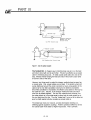
The main power output connector requires a standard HN plug. A typical
combination is an Amphenol part #83-804 (Mil UG59B) and RG-8 cable or
Amphenol part #8125 (Mil UG494) and RG 217 cable. There is no practical
limit to the length of the cable. Use the following instructions to prepare the
cable:
1. Strip the cable; be careful not to nick the braid, the dielectric, or the
conductor.
2. Slip end "A", insulator "B", washer "C", and cone "0" onto the cable.
Push cone "C" all the way onto the outer insulation. Cut the braided
shield 0.25 in. from the cone.
3. Roll the braided shield back over cone "0". Cut the inner insulation and
the center conductor to the dimensions shown.
4. Solder the tip to the center conductor.
5. Attach the outer cover.
6. Conduct a high-potential test for the insulation. Hi-pot the insulation to
3 kV dc between the center conductor and the outside shield.
~Y-O-U---
SHOULD KNOW•••
(Dp
When conducting a high-potential test, high
voltages are present. Use extreme caution.
1 r•
l--
.25
.35
®
I
A
1.25 . ,
.25
@)
C
0
.....
G)
Figure 3-1. Preparing the RG-B coaxial cable.
3-6
B
..... ..... ..... .....
EI:P>
PREPARING FOR USE
The unit is shipped with a dc-blocking capactor in series with the center
lead of the output connector. The capacitor is rated for full-output current
and 400 V of de bias or self bias of ether polarity. The output connector
shield is normally shipped grounded via a ground strap on the inside of the
connector. If a floating output is required, this ground strap may be removed.
Connecting the User 110 Interface
The I/O connector attached to the rear of the supply is internally wired to
allow preliminary operation from the front panel. Plug this connector into the
15-pin D connector at the rear of the unit. Figure 3-2 shows the rear panel.
Circuit Breaker
©
0
©
0
@
c:==::J
c:==::J
c:==::J
c:==::J
c:==::J
c:==:::=>
c:==::J
c:==::J
c:==::J
c:==::J
c:==::J
c:==::J
c:==::J
c:==::J
c:==::J
c:==::J
c:==::J
c:==::J
c:==::J
c:==::J
c:==::J
c:==::J
c:==::J
c:==::J
c:==::J
c:==::J
c:==::J
c:==::J
c:==::J
c:==::J
c:==::J
c:==::J
c:==::J
c:==::J
c:==::J
c:==::J
c:==::J
c:==::J
00
@
c:==::J
c:==::J
c:==::J
c:==::J
c:==::J
c:==::J
c:==::J
@~}2l
c:==::J
c:==::J
c:==::J
c:==::J
c:==::J
c:==::J
c:==::J
.............
@ e
User Connector
Input Line Cord
Ground Stud
Figure 3-2. Rearpanel.
3-7
0
@
@V!::::~:I@
Output Connector
@
0
3-8
PREPARING FOR USE
FIRST-TIME OPERATION
Selecting Two-wire or Three-wire Control
You can select ether a two-wire or a three-wire configuration for controlling
the output onloff in remote mode. In the two-wire configuration, XOFF.D
(pin 14) and XSON.D (pin 15) function as one input; in the three-wire
configuration they function independently. For information on selecting
remote mode, see the Choosing Modes section on page 4-3.
Both XSON.D and XOFF.D are pulled up through a 10 kQ resistor, so an
open circuit is a sufficient high-logic level. A contact closure to POWCOM is
a sufficient low-logic level.
As a safety feature, the OUTPUT ON/OFF switch on the front panel will turn
the output off while the unit is operating in remote mode. If you use
three-wire control, the output remains off until you turn it on again. However,
if you use two-wire control, the front panel OUTPUT ON/OFF switch keeps
the output off only as long as you hold the swtch in the OFF position.
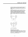
Two-wire control
In a two-wire configuration, a closed contact swtch pulls both XSON.D and
XOFF.D low and turns the output on. An open switch pulls both XSON.D
and XOFF.D high and turns the output off. Figure 3-3 shows the wiring
diragram for two-wire control.
3-9
d2CS
PART II
- - - .. . . . . . . . . . . . . . . . . . . .- - - - - - - - - - - - - - - - - - - -
POWCOM
INTLK.D
7
XOFF.D
14
XSON.D
15
Figure 3-3. Wiring diagram for two-wire control.
Three-wire control
In a three-wire configuration, the momentary contact switch between XOFF.D
and POWCOM is normally closed and the momentary contact switch
between XSON.D and POWCOM is normally open. Fig. 3-4 shows the wiring
diragram for three-wire control.
When you first turn the POWER switch to ON, the output is off; a
momentary contact closure between XSON.D and POWCOM turns the
output on. When the output is on, a momentary open contact between
XOFF.D and POWCOM turns the output off.
Figure 3-4. Wiring diagram for three-wire control.
3 - 10
PREPARING FOR USE
Switch Options for Three-Wire Control
To control output on/off in remote control, you can use ether one
3-position, double-pole swtch, or two z-poston, single-pole switches.
Fig. 3-5 shows the wiring diagram for the three-position switch. Table 3-1
shows the output states that result from the three possible switch positions.
As shown in Table 3-1, you turn the output on by making momentary
contact at switch B, thus closing the circuit between XSON.D and
POWCOM. You turn the output off by making momentary contact at switch
A, thus opening the circuit between XOFF.D and POWCOM. The stable
(middle) poston maintains the normal contact postons and the unit remains
on or off depending on what you most recently selected.
INTLK.D
7
Normally Closed
A
POWCOM
XOFF.D
14
I
XSON.D
1..
15 O - - - - - - - - - - - ' l O
I'~------..
8
Normally Open
Figure 3-5. Wiring diagram for three-position, double-pole switch.
Table 3-1. Truth table for one 3-position swtch showing switch contact states
and resutting power output state.
Switch
Switch
Position
Position State Contact State Contact State Output State
Switch A
Switch B
Power
momentary
contact
closed
closed
on
2
stable
closed
open
last state
selected
3
momentary
contact
open
open
off
3 - 11
PART II
d2-(8)---......................--------------------
Fig. 3-6 shows the wiring diagram for the two 2-position switches. Table 3-2
shows the output states resulting from the four possible combinations of the
switch position states. As with the three-position switch, momentary contact
at switch B closes the circutt between XSON.D and POWCOM and turns the
output on. Momentary contact at switch A opens the circut between XOFF.D
and POWCOM and turns the output off.
However, pulling XSON.D low turns the output on only ~ the momentary
contact switch between XOFF.D and POWCOM is in its normal position
(closed). Therefore, if both switches are held in their momentary positions,
the off swtch overrides the on swtch,
INTLK.D
7
OLJ------it----------------,
Normally Closed
-
POWCOM
A
XOFF.D
14
XSON.D
15 0 - - - - - - - - - - - 1 0 £=>----------'
OLJ--------------------'
..L
B
Normally Open
Figure 3-6. Wiring diagram for two 2-position, single-pole switches.
Table 3-2. Truth table for two 2-position swtches showing the power output
states that result from the four possible combinations of the switch contact
states.
Possible
Switch
Combination
Switch A
Position State
(Contact Statm
Switch B
Position State
(Contact State)
Power
Output
State
momentary
(open)
stable (open)
off
2
stable (closed)
momentary
(closed)
on
3
momentary
(open)
momentary
(closed)
off
4
stable (closed)
stable (open)
last state selected
3 - 12
PREPARING FOR USE
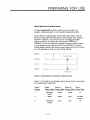
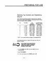
Selecting Tap Numbers and Establishing
Setpoint
The PE internal bad-matching transformer contains ten taps. These taps
albw the PE to transfer power efficiently to a wide range of oads, The taps
provide the following matching capabillies:
Tap
Turns Ratio
10
9
8
7
6
5
1 to 2.53
1 to 2.18
1 to 1.88
1 to 1.62
1 to 1.40
1 to 1.21
1 to 1.04
1 to .90
1 to .76
1 to .67
4
3
2
1
Load
Impedance
Range (Ohms)
1006.4 - 696.19
747.33 - 516.98
556.43 - 384.92
414.29 - 286.59
308.46 - 213.38
229.67 - 158.87
171.00 - 118.29
127.32 - 88.07
94.80 - 65.58
70.58 - 48.82
Load RMS Voltage
Range at full power
(1700 W)*
1308 - 1087.9
1127.15 - 937.48
972.59 - 808.92
839.22 - 698.00
724.15 - 602.29
624.85 - 519.70
539.16 - 448.43
465.23 - 386.94
401.44 - 333.88
346.39 - 288.10
* NOTE: Your can read the bad rms voltage on the displayMONITOR.
Use the following procedure to determine the proper tap number and
establish the setpoint:
Never change the tap number while the
output po_ •• enabled. Changing tap
settings while applying output
damag.. the po_ supply.
pow.
1. Turn the POWER switch OFF and set the LEVEL knob fully
counterclockwise.
2. select TAP NUMBER 1.
3. Turn the circuit breaker and the POWER switch to ON.
3 - 13
PART
82----~
8
II
. . . . . . . . . .- - - - - - - - - - - - - - - - - - -
At this time, the display MONITOR, and the LOCAL and INTERLOCK
status indicators should light. If the REMOTE indicator lights instead of
the LOCAL indicator, see the Troubleshooting section on page 5-7. If
the INTERLOCK status indicator fails to light, check to confirm that the
interlock string is satisfied.
4. Move the OUTPUT ON/OFF rocker switch momentarily to ON. You
should hear a contactor close, and the OUTPUT status indicator should
light.
5. Move the LEVEL knob clockwise until the MONITOR reads
approximately 1QOA> of full output (170 W). The PLASMA and
SETPOINT status indicators should light.
6. To check the output voltage or current, move the DISPLAY rocker
switch to either the VOLTAGE or CURRENT setting.
7. Make sure the SETPOINT status indicator is lit. Gradually advance the
LEVEL control knob to the desired power level.
If the SETPOINT indicator light flashes before you reach the desired
power level, turn off the supply and increase the TAP NUMBER by
one setting. Slowly increase the power until you reach the desired
power level or the SETPOINT indicator light flashes.
Repeat this process until you reach operating power without the
SETPOINT light flashing.
NOTE: If the SETPOINT indicator light flashes
in tap 1. and when you change to tap 2 the light
continues flashing and the power level drops.
the load Impedance Is too low to deliver power
to the load. Contact AE Customer Service for
assistance.
If you reach tap 7. and you cannot obtain the
operating power level before the SETPOINT
Indicator light flashes. check the output voltage.
If the output voltage is greater than 1200 V. the
load Impedance Is too high for the power
supply to deliver power to the required load.
Contact AE Customer Service.
3 - 14
PREPARING FOR USE
8. Increase the power 100/0 over the desired power level. If the
SETPOINT light does not flash you have the correct TAP NUMBER. If
the SETPOINT light does flash increase the TAP NUMBER by one.
9. When you reach the desired power level. lock the LEVEL control knob
by turning the locking skirt clockwise. The supply can be turned off
and on. and the power will return to setpoint automatically.
3 - 15
d2--ilPABLJj- - - - - - - e
3 - 16
CONTENTS
Remote Control
4-3
Units built prior to 2/6/89
4-3
Units built after 2/6/89
4-3
4-1
4-2
REMOTE CONTROL
For units built prior to 2/6/89
1. Before removing the plastic safety shield, turn off the supply and let it
sit for 5 min. before beginning work.
2. Unscrew the six phillips screws from the top of the power supply and
remove the metal cover.
3. Remove the plastic plexiglass safety shield.
4. Three small DIP switches will be visible on the logic board (with the
supply facing forward, the logic board faces the left side of the supply).
The left switch controls the output on/off, the middle switch controls
the REMOTE and LOCAL indicators on the STATUS display, and the
right switch controls the signal source for programming power level.
"Up" or C1 is for local operation and "down" or C2 is for remote
operation. The DIP switches may be set in any combination. After
adjusting the switches, replace the plexiglass cover.
For units built after 2/6/89
1. Turn the OUTPUT ON/OFF swtch OFF.
2. For remote operation of the output power, use a standard screwdriver
to rotate the adjustable switch located directly under OUTPUT ON/OFF
switch on the front panel to REMOTE.
3. For remote operation of the signal for programming power level, rotate
the switch located directly under the LEVEL knob on the front panel to
REMOTE.
If ether of the LOCALIREMOTE swtches are in the REMOTE position, the
LOCAL indicator light in the STATUS display turns off and the REMOTE
indicator lights.
4-3
4-4
PART III
SERVICING YOUR
PE SERIES GENERATOR
CALIBRATION AND TROUBLESHOOTING
CONTENTS
Calibration . . . . . . . . . . . . . . . . . . . . . . . . . . . . . . . . . . . . . . . . . .. 5-5
Removing the Top Cover of the Supply
5-5
Zeroing the Display Monitor
5-5
Maximum Power
Troubleshooting
5-3
5-5
5-7
d2~
PART III
5-4
CALIBRATION AND TROUBLESHOOTING
CALIBRATION
Removing the Top Cover of the Supply
Unscrew the six phillips screws from the top of the power supply and
remove the metal cover.
Zeroing the Display Monitor
The screws used to make the zeroing adjustment are accessible through the
holes in the plexiglass cover. P ZERO = Power Monitor; V ZERO =
Vottage Monitor; I ZERO = Current Monitor
1. Before making any zeroing adjustments, turn the POWER ON/OFF
switch to ON, turn the OUTPUT ON/OFF switch to OFF, and remove
the metal cover. Leave the plexiglass cover in place and let the supply
sit for at least 3 min.
2. For each value, turn the appropriate screw adjustment using a small
standard screwdriver until the front panel display monitor reads zero.
3. Replace the top cover and the six screws.
Maximum Power
The maximum power adjustment clamps the output power to a
predetermined limit, independent of local or remote programming. The MAX
PWR potentiometer is accessible through the holes on the plexiglass cover.
1. Using the LEVEL knob on the front panel or the appropriate user I/O
signal to set the power to just above the maximum desired operating
level.
2. While operating at this level, turn the control MAX PWR potentiometer
counterclockwise until the displayed power is at the desired clamp point.
5-5
dEe
PART III
5-6
CALIBRATION AND TROUBLESHOOTING
TROUBLESHOOTING GUIDE
~-YO-U---
SHOULD KNOW•••
All servicing functions involving input and
output connections can expose you to lethal
voltages. Make sure you take proper safety
precautions before you troubleshoot the
power supply.
These troubleshooting suggestions are included for your convenience. They
are only intended to deal with minor problems. If these troubleshooting tips
fail to correct problems wth the operation of the power supply, please
contact the Advanced Energy Industries, Inc. Customer Service Department
at:
(303) 221-4670
or at AE's 24 hour service hotline:
(303) 221-0108
Symptom
Things To Check/Remedy
No front panel lights
Make sure the input power cord is connected
to appropriate power source.
See the Connecting Input section on page
3-5 for appropriate power
source/requirements.
Make sure the circuit breaker on the rear of
the power supply is ON.
Make sure the front panel POWER switch is
ON.
5-7
428
PART III
--------------------------------------
No STATUS lights except
REMOTE or LOCAL.
Make sure the 110 connector on the rear
panel is connected.
Make sure the pin connections for the 110
plug are correct. See page 2-13 for on
explanation of XOFF (pin 14).
INTERLOCK light is
flashing.
Check to see if interlock string is complete. If
not, see page 2-12 (pin 7) for an explanation
of the interlock string requirements.
Output of power supply
won't turn on.
Check the first two troubleshooting
suggestions (No front panel lights and No
STATUS lights except REMOTE or LOCAL).
If output still won't come on, make sure the
REMOTE/LOCAL status indicators on front
panel are in the desired positions. See the
Remote Control section on page 4-3.
No PLASMA indication on
STATUS display.
Make sure the output cable is attached to the
rear of the supply.
Make sure the vacuum system is at desired
pressure.
Make sure the correct power level is
programmed into the supply.
If not, use the LEVEL knob or user 110
interface to set the power level to the desired
setpoint. See the First Time Operation section
beginning on page 3-9.
Verify the voltage output indicated on the
MONITOR display.
Cannot achieve desired
power level, but neither the
ARC or SETPOINT
indicators on STATUS
display are flashing.
Make sure the maximum power adjustment is
set correctly. See the Maximum Power
section on page 5-5.
5-8
CALIBRATION AND TROUBLESHOOTING
Cannot achieve full output
power and ARC and
SETPOINT indicators on
STATUS display are
flashing.
Disconnect output cable from power supply
and enable the output. If the ARC indicator is
still flashing, call AE Customer Service.
Check the system or chamber for low
impedance to ground. If a low impedance to
ground is present, the problem must be
corrected before the supply will function
properly.
Reconnect the power supply to the system.
Turn OUTPUT switch ON. If the ARC
indicator is still flashing, lower the power level
by 20%. After lowering the power level, if the
ARC indicator is no longer flashing, see the
Selecting Tap Numbers section on page
3-13. If the ARC indicator is still flashing, call
AE Customer Service.
Cannot achieve full power
and SETPOINT indicator
on STATUS display is
flashing.
Move the DISPLAY switch on the front panel
to VOLTAGE. If the voltage displayed on the
MONITOR is above or below the voltage
range specified on page 3-13, see the
Selecting Tap Numbers section on page 3-13.
If the voltage is within the voltage range
specified on page 3-13, call AE Customer
Service.
OVERTEMP indicator on
Make sure fans are operating and not
STATUS display is flashing. blocked. Turn the supply off and call AE
Customer Service.
5-9
5 - 10
PART IV
LEARNING MORE ABOUT
YOUR PE GENERATOR
di:~
PART IV
HOOK-UP NOTES
GROUNDING
Current seeks the path of lowest resistance. If several paths are
characterized by similar impedances, the current flow may randomly switch
paths. This sw~ching may appear as oscillations and cause interference
("noise") with electronic equipment. The goal in any system design is to
provide a known, fixed, lowest impedance path. The way to do this is to
provide good grounding.
Grounding is important for a variety of reasons:
•
it ensures safety of personnel
•
it protects equipment
•
it is necessary for agency approvals
•
it prevents electromagnetic radiation
•
it prevents electromagnetic interference
•
it provides a known reference for control signals
Grounding requirements and standards are set and promulgated by various
commercial and governmental agencies. Information is available from UL,
CSA, VDE, FCC, IEEE, SAE, CISPR, and many local government agencies.
Always check whatever documents are mandated by your local authorities.
This note is intended to provide a broad overview of grounding issues and
considerations.
AC and DC Grounding
In the real world there is a significant difference between the techniques
used to provide a good dc ground and those used to provide a good ac
ground. Just because a system has a very low dc resistance to
earth-ground does not at all imply that ~ has a good ac earth-ground, or
vice versa. A dc ground connection requires conductors and connectors
with adequate cross-sectional area for the current to be carried; these
conductors and connectors must also be made of material with very little
resistance.
An ac ground requires conductors and connectors with adequate surface
area for the current to be carried; however, the conductors and connectors
must also have very little inductive reactance or capacitive reactance to
ensure the lowest possible impedance. This becomes more critlcal as the
frequency increases into the RF range.
6-3
8
82
PART IV
- -- -- -- -- -- -- -- -- -- -- -- -- --
The major safety issue concerning improperly grounded equipment is that
people can come in contact wtth dangerous vottages. Although this danger
is usually viewed as being caused by dc or 50/60 Hz ac voltages, this is not
necessarily the case. The multimeter is a typical measuring instrument used
to determine whether or not a system or component is grounded. A
muttimeter is designed to measure dc voltage and current, ac voltage and
current, and resistance. However, tt is not senstlve to high-frequency energy
and often will not even detect the presence of RF energy, much less give
accurate readings. Since RF can be present without being detected by
common means, there Is a significant potential for harm to personnel
from RF surface burns, arcs that penetrate the skin, and other such
InJuries.
Equipment designed to measure RF energy is expensive and bulky, and
must be calibrated over narrow frequency ranges. Most facilities do not have
this kind of equipment on hand. It is therefore very important that all
appropriate personnel (those involved in design, installation, maintenance,
and operations) are knowledgeable about all aspects of grounding for
electrical energies, from dc through RF.
A-yo-u----
SHOULD KNOW •••
DANGERI Operating and maintenance
personnel must have the correct training
before setting up and maintaining
high-energy electrical equipment.
While significant numbers of RF problems are caused by improper
grounding of RF power supplies used in a process, all plasma systems
produce rome RF energy that must be taken into acount when the system is
designed. As examples: Plasma arcs are like small lightening bolts that
cause broad-band RF interference; a plasma chamber is a type of oscillator
and radiates RF energy if not shielded; electric motors/relays/solenoids can
produce RF energy when they are actuated; even microcomputers used in
instruments and controllers can produce RF energy that can cause problems
with other circuits. Each one of these sources may interfere with the proper
operation of electronic instruments and controls within the system. In the
worst cases, this energy can cause noise in equipment at some distance
from the source, often hundreds of feet or more away.
Symptoms of Noise Problems
Some grounding problems are inevitable in complex and high-power
systems. A good system developer understands grounding problems and,
therefore, has a development lab with good earth grounds. This ensures that
the new system works well during construction and testing. However, a
common occurence is that when it is installed at a customer's site, nothing
works. This is typically due to poor earth-grounding techniques.
6-4
HOOK-UP NOTES
Similarly, noise problems will not always surface during the development
phase of the components that will be used in the system. This is because a
manufacturer cannot simulate the exact environment in which the
components (power supplies, for instance) will be used. Noise problems
tend not to show up until the component is installed and operating in its
intended environment. Then, after a few minutes or hours of normal
operation, the system finds itself someplace out in left field. Inputs are
ignored and outputs are gibberish. The system may respond to a reset, or it
may have to be turned off and then back on again, at which point it
commences operating as though nothing had happened. There may be an
obvious cause, such as an electrostatic discharge from somebody's finger to
a keyboard, or the upset occurs every time another machine is turned on or
off. Or there may be no obvious cause, and nothing the operator can do
will make the upset repeat itself. But a few minutes, or a few hours, or a
few days later it happens again.
One symptom of electrical noise problems is randomness, both in the
occurrence of the problem and in what the system does in its failure. All
operational upsets that occur at seemingly random intervals are not
necessarily caused by noise in the system. Marginal bus voltages,
inadequate decoupling, rarely encountered software conditions, or timing
coincidences can produce upsets that seem to occur randomly. On the
other hand, some noise sources can produce upsets downright periodically.
Nevertheless, the more difficult it is to characterize an upset as to cause and
effect, the more likely it is to be a noise problem.
Types and Sources of Electrical Noise
The name given to electrical noises other than those that are inherent in the
circuit components (such as thermal noise) is EMI: electromagnetic
interference. Motors, power switches, fluorescent lights, electrostatic
discharges, etc., are sources of EMI. There is a veritable alphabet soup of
EMI types, and these are briefly described below.
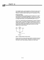
Supply Line Transients
Anything that switches heavy current loads on to or off of ac or dc power
lines will cause large transients in these power lines. Switching a vacuum
pump on or off, for example, can put a large voltage spike onto the ac
power lines.
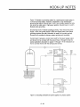
The basic mechanism behind supply line transients is shown in Fig. 1. The
battery represents any power source, ac or dc. The coils represent the line
inductance between the power source and the switchable loads R1 and R2.
If both loads are drawing current, the line current flowing through the line
inductance establishes a magnetic field of some value. Then, when one of
the loads is switched off, the field due to that component of the line current
6-5
d2
8
PART IV
- -- -- -- -- -- -- -- -- -- -- -- -- --
collapses, generating transient voltages, v = L(di/dt), which try to maintain the
current at its original level. That's allied an "inductive kick." Because of
contact bounce, transients are generated whether the switch is being
opened or closed, but they're worse when the switch is being opened.
L
v
L
Figure 1. Supply line transients.
An inductive kick of one type or another is involved in most line transients.
Other mechanisms for line transients exist, involving noise pickup on the
lines. The noise voltages are then conducted to a susceptible crcut right
along with the power.
EMP and RFI
Anything that produces arcs or sparks will radiate electromagnetic pulses
(EMP) or radio-frequency interference (RFI). Spark discharges have
probably caused more software upsets in digital equipment than any other
single noise source. The upsetting mechanism is the EMP produced by the
spark. The EMP induces transients in the circuit, which are what actually
cause the upset.
Arcs and sparks occur in plasma chambers, electron-beam systems, and
magnetron sputtering systems; in associated equipment such as electric
motors and switches; and in static discharges. Electric motors that have
commutator bars produce an arc as the brushes pass from one bar to the
next. Dc motors and the "universal" (ac/dc) motors that are used to power
hand tools are the kinds that have commutator bars. In switches, the same
inductive kick that puts transients on the supply lines will cause an opening
or closing switch to throw a spark. Vacuum systems contain vacuum pumps,
solenoid valves, motors, power supplies, and many other noise producers.
ESD
Electrostatic discharge (ESD) is the spark that occurs when a person picks
up a static charge from walking across a carpet, and then discha.rges it into
a keyboard, or whatever else can be touched. Walking across a carpet in a
dry climate, a person aln accumulate a static voltage of 35 kV. The current
6-6
HOOK-UP NOTES
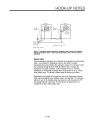
pulse from an electrostatic discharge has an extremely fast rise time typically, 4 A/nsec. Figure 2 shows ESD waveforms that have been
observed by some investigators of ESD phenomena.
80
- - Experimental
CJ)
Q.
E
60
- - Calculated
«
c
+oJ
c
40
~
:J
U
20
o
o
10
20
30
40
50
60
70
80
90 100 110 120
Time in Nanoseconds
(a)
Vert: 5 A/Div
Time: 5 ns/Div
-
I
I
I
-500 mV
I
5 ns- -
"J \../' j\
Displayed:
I p : 40 A
r.. 1 ns
500 V
~
J\
~
.....,
--....,~
(b)
Figure 2. Waveforms of electrostatic discharge currents from a hand-held metallic
aDject.
It is enlightening to calculate the L(di/dt) voltage required to drive an ESD
current pulse through a couple of inches of straight wire. Two inches of
straight wire has about 50 nH of inductance. That's not very much, but
using 50 nH for Land 4 Alnsec for di/dt gives an L(di/dt) drop of about
200 V. Recent observations by W.M. King suggest even faster rise times
(Fig. 28) and the occurrence of muttiple discharges during a single
discharge event.
Obviously, ESD sensitivity needs to be considered in the design of
equipment that is going to be used in difficult industrial environments.
A~hough humidity is controlled in many Ie clean rooms, this is not the case
in many other clean rooms. Any time large volumes of air are moved,
electrostatic energy will build up. This can cause ESD problems for a
6-7
d2
8
PART IV
- -- -- -- -- -- -- -- -- -- -- -- -- -
system's control circu~ry, whether in the system computer, a power supply's
microprocessor, an electronic vacuum pump, or a critical endpoint detector
such as an RGA computer.
Ground Noise
Currents in ground lines are another source of noise. These can be 60-Hz
currents from the power lines, or RF hash, or crosstalk from other signals
that are sharing this particular wire as a signal return line. Noise in the
ground lines is often referred to as a "ground loop" problem. The basic
concept of the ground loop is shown in Fig. 3. The problem is that true
earth-ground is not really at the same potential in all locations. If the two
ends of a wire are earth-grounded at different locations, the voltage
difference between the two "ground" points can drive significant currents
(several amperes) through the wire. Consider the wire to be part of a loop
which contains, in addition to the wire, a voltage source that represents the
difference in potential between the two ground points, and you have the
classical "ground loop." By extension, the term is used to refer to any
unwanted (and often unexpected) currents in a ground line.
Earth-ground
at A
Ground
Figure 3. Illustration of a ground loop.
"Radiated" and "Conducted" Noise
Radiated noise is noise that arrives at the victim circut in the form of
electromagnetic radiation, such as EMP and RFI. It causes trouble by
inducing extraneous votaces in the circuit. Conducted noise is noise that
arrives at the victim crcut already in the form of an extraneous voltage,
typically via the ac or dc power lines.
You can defend against radiated noise by carefully designing layouts and
using effective shielding techniques. You can defend against conducted
noise with fitters and suppressors, although layouts and grounding
techniques are important here, too.
6-8
HOOK-UP NOTES
Types of Failures and Failure Mechanisms
A major problem that EMI can cause in digital systems is intermittent
operational malfunction. These software upsets occur when the system is in
operation at the time an EMI source is activated, and are usually
characterized by a loss of information or a jump in the execution of the
program to some random location in memory. The person who has to iron
out such problems is tempted to say the program counter went crazy.
There is usually no damage to the hardware, and normal operation can
resume as soon as the EMI has passed or the source is de-activated.
Resuming normal operation usually requires manual or automatic reset, and
possibly re-entering of lost information.
Electrostatic discharges from operating personnel can cause not only
software upsets, but also permanent ("hard") damage to the system. For
this to happen the system doesn't even have to be in operation. Sometimes
the permanent damage is latent, meaning the initial damage may be
marginal and require further aggravation through operating stress and time
before permanent failure takes place. Sometimes the damage is hidden.
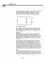
Current Loops
The first thing most people learn about electrictty is that current won't flow
unless it can flow in a closed loop. This simple fact is sometimes temporarily
forgotten by the overworked engineer who has spent the past several years
mastering the intricacies of the DO loop, the timing loop, the feedback loop,
and maybe even the ground loop.
g-mu-~
SHOULD KNON ...
The simple current loop probably owes its apparent
demise to the invention of the ground symbol. By a
stroke of the pen you avoid having to draw the
return paths of most of the current loops in the
circuit. Then "ground" turns into an infinite current
sink, so that any current that flows into it is gone
and forgotten. Forgotten it may be, but it's not
gone. It must return to its source, so that its path
will by all the laws of nature form a closed loop.
The physical geometry of a given current loop is the key to why tt generates
EMI, why it's susceptible to EMI, and how to shield it. Specifically, it's the
area of the loop that matters.
Any flow of current generates a magnetic field with an intensity that varies
inversely to the distance from the wire that carries the current. Two parallel
wires conducting currents + I and -I (as in signal feed and return lines)
would generate a nonzero magnetic field near the wires if the distance from
6-9
d2
8
PART IV
- -- -- -- -- -- -- -- -- -- -- -- -- --
a given point to one wire is noticeably different than the distance from the
same point to the other wire, but farther away (relative to the wire spacing).
Where the distances from a given point to either wire are about the same,
the fields from both wires tend to cancel out.
Thus, maintaining proximity between feed and return paths is an important
way to minimize their interference wtth other signals. The way to maintain
their proximty is essentially to minimize their loop area. And, because the
mutual inductance from current loop A to current loop B is the same as the
mutual inductance from current loop B to current loop A, a circuit that
doesn't radiate interference doesn't receive it either.
Thus, from the standpoint of reducing both generation of EMI and
susceptibility to EMI, the hard rule is to keep loop areas small. To say that
loop areas should be minimized is the same as saying the circuit inductance
should be minimized. Inductance is by definition the constant of
proportionality between current and the magnetic field it produces: ¢ = LI.
Holding the feed and return wires close together so as to promote field
cancellation can be described either as minimizing the loop area or as
minimizing L. It's the same thing.
Shielding
There are three basic kinds of shields: shielding against capacitive coupling,
shielding against inductive coupling, and RF shielding. Capacitive coupling is
electric field coupling, so shielding against tt amounts to shielding against
electric fields. As will be seen, this is relatively easy. Inductive coupling is
magnetic field coupling, so shielding against tt is shielding against magnetic
fields. This is a little more difficult. Strangely enough, this type of shielding
does not in general involve the use of magnetic materials. RF shielding, the
classical "metallic barrier" against all sorts of electromagnetic fields, is what
most people picture when they think about shielding. Its effectiveness
depends partly on the selection of the shielding material, but mostly, as it
turns out, on the treatment of its seams and the geometry of its openings.
Shielding Against Capacitive Coupling
Capacitive coupling involves the passage of interfering signals through
mutual or stray capacitances that aren't shown on the circuit diagram, but
which the experienced engineer knows are there. Capacitive coupling to
your body is what would cause an unstable oscillator to change its
frequency when you reach your hand over the circuit, for example. More
importantly, in a digital system it causes crosstalk in multi-wire cables.
The way to block capacitive coupling is to enclose the circuit or conductor
you want to protect in a metal shield. That's called an electrostatic or
Faraday shield. If coverage is 1000/0, the shield does not have to be
6 - 10
HOOK-UP NOTES
grounded, but ~ usually is, to ensure that circuit-to-shield capacitances go to
signal reference ground rather than acting as feedback and crosstalk
elements. Besides, from a mechanical point of view, grounding it is almost
inevitable.
A grounded Faraday shield can be used to break capactive coupling
between a noisy circuit and a victim circuit, as shown in Fig. 4. Figure 4A
shows two circuits capacttively coupled through the stray capacitance
between them. In Figure 4B the stray capacitance is intercepted by a
grounded Faraday shield, so that interference currents are shunted to
ground. For example, a grounded plane can be inserted between PCBs
(printed circuit boards) to eliminate most of the capacitive coupling among
them.
Noise
Source
----------1 1-----------
Victim
Circuit
(a) Capacitive Coupling
rFaraday Shield
Noise
Source
-----1 1--- ---I 1----
Victim
Circuit
~
-(b) Electrostatic Shielding
Figure 4. Use of Faraday shield.
Shielding Against Inductive Coupling
With inductive coupling, the physical mechanism involved is a magnetic flux
density B from some external interference source that links with a current
loop in the victim circuit, and generates a votaae in the loop in accordance
with Lenz's law: v = NA(d B/dt), where in this case N = 1 and A is the
area of the current loop in the victim circuit.
6 - 11
PART IV
d2~---------------------------
There are two aspects to defending a circuit against inductive coupling.
One aspect is to try to minimize the offensive fields at their source. This is
done by minimizing the area of the current loop at the source so as to
promote field cancellation, as described in the section on current loops. The
other aspect is to minimize the inductive pickup in the victim crcuh by
minimizing the area of that current loop, since, from Lenz's law, the induced
vottage is proportional to this area. So the two aspects really involve the
same corrective action: Minimize the areas of the current loops. In other
words, minimizing the offensiveness of a circu~ inherently minimizes its
susceptibility.
Shielding against inductive coupling means nothing more nor less than
controlling the dimensions of the current loops in the crcut. We will look at
two examples of this type of "shielding": the coaxial cable and the twisted
pair.
The Coaxial cable. Figure 5 shows a coaxial cable carrying a current I
from a signal source to a receiving load. The shield carries the same
current as the center conductor. Outside the shield, the magnetic field
produced by + I flowing in the center conductor is cancelled by the field
produced by -I flowing in the shield. To the extent that the cable is ideal in
producing zero external magnetic field, ~ is immune to inductive pickup from
external sources. The cable effectively adds zero area to the loop. This is
true only Wthe shield carries the same current as does the center conductor.
R
I'--__J -. -=i
Current Loop
Figure 5. External to the shield, f/J
=
0
In the real world, both the signal source and the receiving load are likely to
have one end connected to a common signal ground. In that case, should
the cable be grounded at one end, both ends, or nether end? The answer
is that it should be grounded at both ends. Figure 6A shows the situation
when the cable shield is grounded at only one end. In that case the current
loop runs down the center conductor of the cable, then back through the
common ground connection. The loop area is not well defined. The shield
not only does not carry the same current as the center conductor, but it
doesn't carry any current at all. There is no field cancellation at all. The
shield has no effect whatsoever on either the generation of EMI or
susceptibility to EMI. (It is, however, still effective as an electrostatic shield,
or at least ~ would be if the shield coverage were 1000/0.)
6 - 12
HOOK-UP NOTES
Figure 6B shows the situation when the cable is grounded at both ends.
Does the shield carryall of the return current, or only a portion of tt on
account of the shunting effect of the common ground connection? The
answer to that question depends on the frequency content of the signal. In
general, the current loop will follow the path of least impedance. At low
frequencies, a Hz to several kilohertz, where the inductive reactance is
insignificant, the current will follow the path of least resistance. Above a few
kilohertz, where inductive reactance predominates, the current will follow the
path of least inductance. The path of least inductance is the path of
minimum loop area. Hence, for higher frequencies the shield carries virtually
the same current as the center conductor, and is therefore effective against
both generation and reception of EMI.
v
s
R
_
i
t
~Current Loop
~----------------"'
,
l
1-
j
(a) Shield Has No Effect
v
s
R
------------------------7---
I High-frequency
r:: j
Current Path
-= '------------------------'1
I
I
!
l
-----'1
I
!
-=
I
'-------------------~
(b) Two Return Paths
Low-frequency
Current Path
Figure 6. Use of coaxial cable.
Note that we have now introduced the infamous "ground loop" problem, as
shown in Fig. 7A. Fortunately, a digital system has some built-in immunity to
moderate ground loop noise. In a noisy environment, however, you can
break the ground loop and still maintain the shielding effectiveness of the
coaxial cable by inserting an optical coupler, as shown in Fig. 7B. What the
optical coupler does, basically, is allow you to redefine the signal source as
being ungrounded, 00 that the optically coupled end of the cable need not
be grounded; this still lets the shield carry the same current as the center
conductor. Obviously, if the signal source weren't grounded in the first
place, the optical coupler wouldn't be needed.
6 - 13
d2
e
PART IV
- -- -- -- -- -- -- -- -- -- -- -- -- --
R
r---------------------------------------l
JI
(
'-----.
I'-
LGrOUnd Loop
)
r-::
rr::
l"""--~---_-------__t----~--------------J
o
Potential Difference
Between the Two
Ground Points
(a) The Grou nd Loop
R
+5V
r-------,
i
!
I
I
R
i
~
r--O++-OOO+O-------+-+---
~
I
-----~..------------.......
-j
.....
i
~
L..--
"----'-- -
---~~:~-;~~~--~~~~-----l
j
(b) Breaking the Ground Loop
Figure 7. Use of optical coupler.
The Twisted Pair. A cheaper way to minimize loop area is to run the feed
and return wires right next to each other. This isn't as effective as a coaxial
cable in minimizing loop area. An ideal coaxial cable adds zero area to the
loop, whereas merely keeping the feed and return wires next to each other
is bound to add a finite area.
However, two things work to make this cheaper method almost as good as
a coaxial cable. First, coaxial cables are not ideal. If the shield current isn't
evenly distributed around the center conductor at every cross-section of the
cable (it isn't), then field cancellation external to the shield is incomplete.
Since field cancellation is incomplete, the effective area added to the loop by
the cable isn't zero. Second, in the cheaper method the feed and return
wires can be twisted together. This not only maintains their proximity, but
the noise picked up in one twist tends to cancel out the noise picked up in
the next twist down the line. Thus the "twisted pair" turns out to be about as
good a shield against inductive coupling as coaxial cable is.
The twisted pair does not, however, provide electrostatic shielding (i.e.,
shielding against capacitive coupling). Another operational difference is that
the coaxial cable works better at higher frequencies. This is primarily
6 - 14
HOOK-UP NOTES
because the twisted pair adds more capacitive loading to the signal source
than does the coaxial cable. The twisted pair is normally considered useful
up to only about 1 MHz; the coaxial cable is considered useful up to 1 GHz.
RF Shielding
A time-varying electric field generates a time-varying magnetic field, and vice
versa. Far from the source of a time-varying EM field, the ratio of the
amplitudes of the electric and magnetic fields is always 377 Q. Up close to
the source of the fields, however, this ratio can be quite different, and
dependent on the nature of the source. The field where the ratio is near
377 Q is called the far field, and the field where the ratio is significantly
different from 377 Q is called the near field. The ratio itself is called the
wave impedance, E/H.
The near field goes out about one-sixth of a wavelength from the source. At
1MHz this is about 150 ft., and at 10 MHz it's about 15 ft. That means that
if an EMI source is in the same room with the victim circuit, it's likely to be a
near field problem. The reason this matters is that in the near field an RF
interference problem could be almost entirely due to E-field coupling or
H-field coupling, and that could influence the choice of an RF shield or
whether an RF shield will help at all.
In the near field of a whip antenna, the E/H ratio is higher than 377 Q,
which means it's mainly an E-field generator. A wire-wrap post can be a
whip antenna. Interference from a whip antenna would be by electric field
coupling, which is basically capacitive coupling. Methods to protect a circuit
from capacitive coupling, such as a Faraday shield, would be effective
against RF interference from a whip antenna. A gridded-ground structure
would be less effective.
In the near field of a loop antenna, the E/H ratio is lower than 377 Q, which
means it's mainly an H-field generator. Any current loop is a loop antenna.
Interference from a loop antenna would be by magnetic field coupling,
which is basically the same as inductive coupling. Methods to protect a
circuit from inductive coupling, such as a gridded-ground structure, would
be effective against RF interference from a loop antenna. A Faraday shield
would be less effective.
difficu~ case of RF interference, near field or far field, may require a
genuine metallic RF shield. The idea behind RF shielding is that
time-varying EMI fields induce currents in the shielding material. The
2R
induced currents dissipate energy in two ways: 1 losses in the shielding
material and radiation losses as they re-radiate their own EM fields. The
energy for both of these mechanisms is drawn from the impinging EMI fields
-thus the EMI is weakened as it penetrates the shield.
A more
6 - 15
d2
e
PART IV
- -- -- -- -- -- -- -- -- -- -- -- -- -
2R
More formally, the 1 losses are referred to as absorption loss, and the
re-radiation is called reflection loss. As it turns out, absorption loss is the
primary shielding mechanism for H-fields, and reflection loss is the primary
shielding mechanism for E-fields. Reflection loss, being a surface
phenomenon, is pretty much independent of the thickness of the shielding
material. Both loss mechanisms, however, are dependent on the frequency
(co) of the impinging EMI field, and on the permeabiltty (u) and conductivity
(a) of the shielding material. These loss mechanisms vary approximately as
follows:
reflection loss to an E-field (in dB)
a
log cop.
N
absorption loss to an H-field (in dB)
N
t vcoap.
Where:
t = the thickness of the shielding material.
The first expression indicates that 1) E-field shielding is more effective if the
shield material is highly conductive and less effective if the shield is
ferromagnetic, and 2) that low-frequency fields are easier to block than
high-frequency fields. This is shown in Fig. 8.
co
3
0::::
en
(f)
0
~
c
0
:;:;
o
(l)
~
0::::
150
125
100
75
50
25
0
0.01
0.1
1
10
100 1000 10,000
Frequency (Kilohertz)
Figure 8. E-field shielding.
Copper and aluminum both have the same perrneabitty, but copper is
slightly more conductive, and 00 provides slightly greater reflection loss to an
E-field. Steel is less effective for two reasons, First, it has a somewhat
elevated permeability due to its iron content, and, second, as tends to be
the case with magnetic materials, it is less conductive.
On the other hand, according to the expression for absorption loss to an
H-field, H-field shielding is more effective at higher frequencies and with
shield material that has both high conductivity and high permeability. In
practice, however, selecting steel for its high permeability involves some
compromise in conductivity. But the increase in permeabiltty more than
6 - 16
HOOK-UP NOTES
makes up for the decrease in conductivity. as can be seen in Fig. 9. This
figure also shows the effect of shield thickness.
175
m
~
(f)
(f)
0
-.oJ
c:
150
125
100
0
75
0
SD
~
L(f)
.0
-c
25
0
10
Frequency (Hertz)
Figure 9. H.field shielding.
A composite of E-field and H-field shielding is shown in Fig. 10. However.
this type of data is meaningful only in the far field. In the near field. the EMI
could be 9QO/o H-field. in which case the reflection loss is irrelevant. It would
be advisable then to beef up the absorption loss. at the expense of reflection
loss. by choosing steel. A better conductor than steel might be less
expensive. but it would also be ineffective.
m
~
300 . . . . . . . . - - - - - - - - - - - - - , . ,
Plane Wave
(f)
(f)
Q)
250
~
200
w
150
c
Q)
>
~
I
I
I
I
............ ./~
100
Reflection
,
,,
I
•
I
50
~'
Absorption
--'
"
O-+--~-~--';~---r-~-~
0.01
0.1
10
100
1000 1O.000
Frequency (Kilohertz)
Figure 10. E- and H.field shielding.
6 - 17
PART IV
d2~--------------------------A characteristic that can be exploited for low-frequency magnetic fields is the
ability of a high-permeability material such as mumetal to divert the field by
presenting a very low reluctance path to the magnetic flux. Above a few
kilohertz, however, the permeability of such materials is the same as steel.
In actual fact the selection of a shielding material turns out to be less
important than the presence of seams, joints and holes in the physical
structure of the enclosure. The shielding mechanisms are related to the
induction of currents in the shield material, but the currents must be allowed
to flow freely. If they have to detour around slots and holes, as shown in
Fig. 11, the shield loses much of its effectiveness.
As can be seen in Fig. 11, the severity of the detour has less to do with the
area of the hole than it does with the geometry of the hole. Comparing
Fig. 11C wtth Fig. 11D shows that a long narrow discontinutty such as a
seam can cause more RF leakage than a line of holes with larger total area.
A person who is responsible for designing or selecting rack or chassis
enclosures for an EMI environment needs to be familiar wtth the techniques
that are available for maintaining electrical continuity across seams.
Information on these techniques is available in the references at the end of
this note.
Induced
Shield
Current
(a)
Section of
Shield
Rectangular
Slot
(b)
(d)
(c)
Figure 11. Effect of shield discontinuity on magnetically induced shield current.
6 - 18
HOOK-UP NOTES
Grounds
There are two kinds of grounds: earth ground (safety ground) and signal
ground. The earth is not an equipotential surface, 00 earth-ground potential
varies. In addition, tts other electrical properties are not conducive to its use
as a return conductor in a circuit. However, circuits are often connected to
earth ground for protection against shock hazards. The other kind of
ground, signal ground, is an arbttrarily selected reference node in a circuitthe node with respect to which other node voltages in the circuit are
measured.
Earth Ground
The standard U.S. three-wire, single-phase ac power distribution system is
represented in Fig. 12. The white wire is earth-grounded at the service
entrance. If a load circuit has a metal enclosure or chassis, and if the black
wire develops a short to the enclosure, there will be a shock hazard to
operating personnel, unless the enclosure itself is earth-grounded. If the
enclosure is earth-grounded, a short results in a blown fuse rather than a
"hot" enclosure. The earth-ground connection to the enclosure is called a
safety ground. The advantage of the three-wire power system is that it
distributes a safety ground along with the power.
Note that the safety-ground wire carries no current, except in case of a faut,
so that at least for low frequencies it's at earth-ground potential along tts
entire length. The votaue of the white wire, on the other hand, may be
several volts different than the voltage of ground, due to the IR drop along
its length.
,
r
Service
Entrance
(-----------"
Blac k
. '1
/'---------------~
I
i
Load
!
Circuit i
i
I
I
White
I
I
t,......_-------
Metal
Enclosure
!
,,,_____
_
Green
....
,'---------_/
Earth-ground
Figure 12. Single-phase power distribution.
6 - 19
i
"J'
d2
8
PART IV
- -- -- -- -- -- -- -- -- -- -- -- -- --
In high-power systems and systems that radiate high levels of noise, it is
common practice to provide each system with an individual earth-ground.
This is done by driving a copper stake or stakes into the ground under or
very close to the frame of the system, even to the extent of drilling holes
through concrete floors.
In multistory buildings tt is even more difficult to provide a low-impedance,
secure connection to the earth. Many times this is done by using a copper
pipe that provides water to the system. This practice is suspect because the
water pipe may travel a considerable distance before making contact with
the earth, and thus may have a relatively high impedance/resistance. In a
muttistory system, a heavy copper strap should connect the system frame to
an earth-ground stake by the shortest possible path.
All earth-ground connections should be made with 1-1.5 in. copper strap
whenever possible. This practice provides a low-impedance path for both dc
and ac.
In many areas the soil is very dry and has high electrical resistance. This is
cured by providing a grid of stakes or a mat of copper wires, and a means
of continually wetting the earth around the stakes or grid.
In the past, the earth around the ground stake was saturated with copper
sulfate. However, the toxicity of copper sulfate combined with its high
solubility endangers groundwater supplies, and so this practice is now illegal.
Other, nontoxic electrolytes are sometimes used, depending on local laws.
Signal Ground
Signal ground is a single point in a circuit that is designated to be the
reference node for the circuit. Commonly, wires that connect to this single
point are also referred to as "signal ground." In some circles "power supply
common" or PSC is the preferred terminology for these conductors. In any
case, the manner in which these wires connect to the actual reference point
is the basis of distinction among three kinds of signal-ground wiring
methods: series, parallel, and multipoint (shown in Fig. 13).
6 - 20
HOOK-UP NOTES
'-Ref. Point
Connection
~Ref. Point
Parallel Connection
Ref. Point
Multipoint Connection
Figure 13. Three ways to wire the grounds.
The series connection is pretty common because it's simple and economical.
It's the noisiest of the three, however, due to common-ground impedance
coupling between the circuits. When several circuits share a ground wire,
currents from one circuit, flowing through the finite impedance of the
common ground line, cause variations in the ground potential of the other
circuits. Given that the currents in a digital system tend to be spiked, and
that the common impedance is mainly inductive reactance, the variations
could be bad enough to cause bit errors in high current or particularly noisy
situations.
The parallel connection eliminates common-ground impedance problems,
but uses a lot of wire. Other disadvantages are that the impedance of the
individual ground lines can be very high, and the ground lines themselves
can become sources of EMI.
6 - 21
PART IV
d2~--------------------------
In the multipoint system, ground impedance is minimized by using a ground
plane with the various circuits connected to it by very short ground leads.
This type of connection would be used mainly in RF circuits above 10 MHz.
Practical Grounding
A combination of series and parallel ground-wiring methods can be used to
trade off economic and electrical considerations. The idea is to run series
connections for circuits that have similar noise properties, and connect them
at a single reference point, as in the parallel method (shown in Fig. 14).
In Fig. 14, the "noisy and high current signal ground" connects to things like
motors and relays. The hardware ground is the safety-ground connection to
chassis, racks, and cabinets. It's a mistake to use the hardware ground as
a return path for signal currents because it's fairly noisy (for example, it's the
hardware ground that receives an ESD spark) and tends to have high
resistance due to joints and seams.
Quiet
Signal
Ground
Noisy
and High
Current
Signal
Ground
Hardware
Ground
' - Ref. Point
Green-wire
Ground
Figure 14. Parallel connection of series grounds.
Screws and bolts don't always make good electrical connections because of
galvanic action, corrosion, and dirt. These kinds of connections may work
well at first, and then cause mysterious maladies as the system ages.
6 - 22
HOOK-UP NOTES
Figure 15 illustrates a grounding system for a typical power supply setup in
a vacuum-process system, showing an application of the series/parallel
ground-wiring method. Ground lines 1 and 2 are normally required by code
but cannot be relied upon in high-power systems. Ground lines 3, 4, and 5
illustrate series grounding.
Ground lines 6 and 7 illustrate parallel grounding. They ensure that power
supply 1 (PS1) and power supply 2 (PS2) are integral parts of the system
grounding scheme (the utility connection is usually not a quality ground).
Ground line 8 provides the primary system earth-ground connection.
Current return 9 ensures a current return path for the power supply output
and should not be confused with the ground lines (1 through 8). See the
typical applications discussed on pages 1-9 through 1-16 for instructions on
how to connect this line with the earth-ground terminal.
.---------------4. 9
~----------.
Analog
Digital
Suppresion
~
[B-1
[Q}---1
0
PS,
Master
~ ~-.--..o
o0x
o0Y
o0Z
ON
G-Utility
~.n-I--~
_---( 6
~
Internal
~::::::::::::::=r-r----'
PS,
Slave
PS,
Slave
2
o
o
o
"'--------{ 7
Internal
PS
2
Master
o
)-----+------r~.r-+-----/
PS
2
Slave
Figure 15. Grounding connections for power supplies in
6 - 23
a process system.
PART IV
d2~----------------------------------------
The separation of grounds shown in Fig. 16 is similar to what is shown in
Fig. 15, but here tt is shown at the PCB level. Currents in multiplexed LED
displays tend to put a lot of noise on the ground and supply lines because
of the constant switching and changing involved in the scanning process.
The segment driver ground is relatively quiet, since it doesn't conduct the
LED currents. The digtt-driver ground is noisier, and should be provided
with a separate path to the PCB ground terminal, even ~ the PCB ground
layout is gridded. The LED feed and return current paths should be laid out
on opposte sides of the board like parallel flat conductors.
Control Function
VSS
Controller
VCC
Raw
1------ DC
Gro un d .--..
---. ....-
---.
'----
~----a--+--Grou nd
Figure 16. Separate ground for multiplexed LED display.
Figure 17 shows right and wrong ways to make ground connections in
racks. Note that the safety ground connections from panel to rack are
made through ground straps, not panel screws. Rack 1 correctly connects
signal ground to rack ground only at the single reference point. Rack 2
incorrectly connects signal ground to rack ground at two points, creating a
ground loop around points 1, 2, 3, 4, 1.
Breaking the "electronics ground" connection to point 1 eliminates the
ground loop, but leaves signal ground in rack 2 sharing a ground
impedance wlth the relatively noisy hardware ground to the reference point:
In fact, it may end up using hardware ground as a return path for signal
and power supply currents. This will probably cause more problems than
the ground loop.
6 - 24
HOOK-UP NOTES
Rock 1
Rack 2
Ponel
Ponel
Ground
Strops
Primary
Power
Ground
Electronics
Groun~
Green-wire Ground
Figure 17. Electronic circuits mounted in equipment racks should have separate
ground connections. Rack 1 shows correct grounding; rack 2 shows incorrect
grounding.
Braided Cable
Ground impedance problems can sometimes be eliminated by using braided
cable. The reduction in impedance is due to skin effect: At higher
frequencies the current tends to flow along the surface of a conductor rather
than uniformly through its bulk. While this effect tends to increase the
impedance of a given conductor, tt also indicates the way to minimize
impedance-to manipulate the shape of the cross-section so as to provide
more surface area. For tts bulk, braided cable is almost pure surface.
Depending on the length of the cable and the actual frequencies involved,
there may be situations where braided cable is not desirable. The individual
strands of wire in the braided cable may present a high inductance to RF
and actually impede current flow. For high-power RF applications, it is
usually best to use a wide copper strap.
6 - 25
PART IV
d2~---------------------------
Glossary
Digttal ground
Data signal ground
Analog signal ground
Ground-line connections for nondifferentialinput, paired signal wires. These wires are
paired for noise-rejection purposes. The
ground wire of the pair may be connected
to an individual ground connection or to a
common ground connection.
Signal common
Power common
Common return
A return conductor (usually low current)
common to several circuits.
RF return
The path or paths that RF energy uses to
return to its source (such as an RF
generator). RF energy is a surface
phenomenon and may travel over the
surface of insulated wires, chassis, frames,
floors, or equipment faces. Special methods
must be used to ensure that there is a solid
earth-ground in systems that produce or
use RF energy.
Ground
Earth ground
A terminal intended to ensure, by means of
a special connection, the grounding
(earthing) of part of an apparatus when
properly connected to an earth electrode.
Grounding conductor
The conductor that is used to establish
ground and that connects a piece of
equipment or device to the ground
electrode.
Ground electrode
A conductor, group of conductors, mat, or
grid, in intimate contact wtth the earth for
the purpose of providing a connection with
ground. This electrode determines the
lowest ground potential for an electrical
system.
Ground loop
A potentially detrimental loop formed when
two or more points in an electrical system
that are normally at ground potential are
connected by an additional conducting
path.
6 - 26
HOOK-UP NOTES
Earth resistivity
A measurement of the electrical resistance
of a unk volume of soil. The common unit
of measure is the ohm-meter, which is the
resistance measured between faces of a
cubic meter of soil by driving ground
electrodes into the earth 1 m apart to a
depth of 1 m.
Conducted interference
Interference resutting from conducted
radio-frequency noise, switching spikes,
lightening strikes, or conducted electrical
noise (produced by the operation of other
equipment) that enters equipment by direct
coupling.
Radiated interference
Interference resutting from radiated
electromagnetic energy that enters
equipment.
Impedance
Symbol, Z. Unit, ohm (Q). The total
opposition offered by a circuit to the flow of
ac current. It is the vector sum of
resistance and reactance;
Z= R+K
(2:n:;';,; 1}
where:
Z = ac impedance in ohms
R = simple opposition to current flow,
Le., dc resistance, in ohms
j = the square root of -1, an imaginary
number
f = frequency, in Hertz
x = pi, 3.1416, the ratio of the circumference of a circle to its diameter
L = value of circuit inductance, in Henrys
C = value of circuit capacitance, in farads
Symbol, R. Unit, ohm (Q). The simple
opposition to current flow. The "real" part of
impedance. Defined as that factor by which
the mean-square conduction current must
be muttiplied to determine the
corresponding power lost by dissipation as
heat or other permanent radiation loss of
electromagnetic energy from the circuit.
Resistance
6 - 27
PART IV
d2~--------------------------------------
Parting Thoughts
The references by Ott and by White were the main sources of information for
the original article from which most of the material in this note was taken.
According to that article, reference 4 "is probably the finest treatment
currently available on the subject."
Courses and seminars on the subject of electromagnetic interference are
given regularly throughout the year. Information on these can be obtained
from:
IEEE Electromagnetic Compatibility Society
•
EMC Education Committee
345 East 47th Street
New York, NY 10017
Phone: (212) 752-6800
•
Don White Consultants, Inc.
International Training Centre
P. O. Box D
Gainesville, VA 22065
Phone: (703) 347-0030
The EMC Education committee has available a videotape: "Introduction to
EMC - A Video Training Tape," by Henry Ott. Don Whtte Consultants offers
a series of training courses on many different aspects of electromagnetic
compatibiltty. Most organizations that sponsor EMC courses also offer
in-plant presentations.
Reprinted In part by permission of Intel Corporation, Copyright/Intel
Corporation, 1982.
6 - 28
HOOK-UP NOTES
References
1. Clark, O.M. 1979. Electrostatic Discharge Protection Using Silicon
Transient Suppressors. Proceedings of the Electrical Overstress/Electrostatic
Discharge Symposium. Reliability Analysis Center, Rome Air Development
Center.
2. King, W. M. and D. Reynolds. 1981. Personnel Electrostatic Discharge:
Impulse Waveforms Resu~ing From ESD of Humans Directly and Through
Small Hand-held Metallic Objects Intervening in the Discharge Path. In:
Proceedings of the IEEE Symposium on Electromagnetic Compatibility,
pp. 577-590.
3. Ott, H. 1981. Digital Circuit Grounding and Interconnection. In:
Proceedings of the IEEE Symposium on Electromagnetic Compatibility,
pp. 292-297.
4. Ott, H. 1976. Noise Reduction Techniques in Electronic Systems. New
York: Wiley.
5. 1981 Interference Technology Engineers' Master (ITEM) Directory and
Design Guide. R. and B. Enterprises, P. O. Box 328, Plymouth Meeting, PA
19426.
6. Smith, L. Nov. 1979. A Watchdog Circuit for Microcomputer Based
Systems. Digital Design, pp. 78-79.
7. TranZorb Quick Reference Guide. General Semi-conductor Industries,
P.O. Box 3078, Tempe, AZ 85281.
8. Tucker, T.J. 1968. Spark Initiation Requirements of a Secondary
Explosive. Annals of the New York Academy of Sciences, Vol. 152, Article I,
pp. 643-653.
9. White, D. 1973. Electromagnetic Interference and Compatibility, Vol. 3:
EMI Control Methods and Techniques. Don White Consultants.
10. White, D. 1981. EMI Control in the Design of Printed Circuit Boards and
Backplanes. Don White Consultants.
6 - 29
d2~
PART IV
6 - 30
Warranty Claims
Advanced Energy® products are warranted to be free from failures due to defects in material and
workmanship for 12 months after they are shipped from the factory (please see warranty statement,
below, for details).
In order to claim shipping or handling damage, you must inspect the delivered goods and report such
damage to AE within 30 days of your receipt of the goods. Please note that failing to report any damage
within this period is the same as acknowledging that the goods were received undamaged.
For
•
•
•
a warranty claim to be valid, it must:
be made within the applicable warranty period
include the product serial number and a full description of the circumstances giving rise to the claim
have been assigned a return authorization number (see below) by AE Customer Service
All warranty work will be performed at an authorized AE service center (see list of contacts at the front of
the manual). You are responsible for obtaining authorization (see details below) to return any defective
units, prepaying the freight costs, and ensuring that the units are returned to an authorized AE service
center. AE will return the repaired unit (freight prepaid) to you by second-day air shipment (or ground
carrier for local returns); repair parts and labor will be provided free of charge. Whoever ships the unit
(either you or AE) is responsible for properly packaging and adequately insuring the unit.
Authorized Returns
Before returning any product for repair and/or adjustment, call AE Customer Service and discuss the
problem with them. Be prepared to give them the serial number of the unit and the reason for the
proposed return. This consultation call will allow Customer Service to determine if the unit must actually
be returned for the problem to be corrected. Such technical consultation is always available at no charge.
Units that are returned without authorization from AE Customer Service and that are found to be
functional will not be covered under the warranty (see warranty statement, below). That is, you will have
to pay a retest and calibration fee, and all shipping charges.
!!2gradinQ_U_n_it_s
_
AE's products are continually changing as ways to improve them are discovered. AE is happy to
upgrade older units so that they reflect recent improvements. The fee for upgrading a unit will be a
percentage of the current list price, based on the age of the unit. Such an upgraded unit will carry a
6-month warranty (which will be added to any time remaining on the original warranty). Contact
Customer Service for specifics on getting an older unit upgraded to the current revision level.
Warranty
The seller makes no express or implied warranty that the goods are merchantable or fit for any
particular purpose except as specifically stated in printed AE specifications. The sole
responsibility of the Seller shall be that it will manufacture the goods in accordance with its
published specifications and that the goods will be free from defects in material and
workmanship. The seller's liability for breach of an expressed warranty shall exist only if the
goods are installed, started in operation, and tested in conformity with the seller's published
instructions. The seller expressly excludes any warranty whatsoever concerning goods that
have been subject to misuse, negligence, or accident, or that have been altered or repaired by
anyone other than the seller or the seller's duly authorized agent. This warranty is expressly
made in lieu of any and all other warranties, express or implied, unless otherwise agreed to in
writing. The warranty period is 12 months after the date the goods are shipped from AE. In all
cases, the seller has sole responsibility for determining the cause and nature of the failure, and
the seller's determination with regard thereto shall be final.
DElCNmcMI OF CHAJIOE
ORIGINAL ISSUE
PEl16 INDICATED PINS THATGO TO CONTACTOR
10108 C1,3,4 WERE 10\1
PE223 REDRAWN ON CAD WITH NO CHANGE
o
+24
.
0
+15
06
1N4001
+24
J2-2
+24V ~---------"-I
+24
R1S
51
+24
b
C11
.1
CONTACTOR
DRIVE
J2-5
R14
1M
51
C12
.1
05
lN4933
+15V
POW COM~
.,
R17
+24
J2-1
+24
+24
Q1
VN10LM
R15
100K
TO CONTACTOR
J1-6
TO CONTACTOR
J1-4
04
lN4933
C
Q2
+15V
+15V
lC13
TP1
~.1
R19
02
1N4148
R13
~.1
+15
VN10LM
Cl0
C
BUSS OK
1K
2M
+15V
+15Y
3
C9
~.1
1
R1
2K
01
1N4l48
+-_.
TP2
--1
+15
LED 1
+5 REF
J2-J
R2
C7
Rl0
.1
MF
R7
20K
B
R9
-V SENSE
+V SENSE
J1-3 1M, WF
J1-2
R12
1M, MF
R8
1M, MF
R11
,,'
...
4.99K
OVER-
VOLTAGE
i
I
,"
UNOER-
VOLTAGE
20f<, MF
1.
R8
8
1M, MF
+
+15
R4
201<
B
C6
1
SOY
COMPUTER GENERATED DRAWING
AUTOCAD VERSION 10.0
MF'
-I
i
IT£M
MAT NUM8fR
arv
DO NOT SCALE
. . . OTNI. ._ .flfCIND
a......... tKMI.
A
NOTES (UNLESS OTHERWISE SPECIFIED):
1. ALL RESISTORS ARE 1/4W CF, 5~: RESISTANCE VALUES ARE IN OHMS.
2. ALL CAPACITANCE VALUES ARE IN MICROFARADS.
CWE
[)(SQtEO
T1Tlf
L • ±0030
PMTI1Q II FE Of .UMI
IM.U AUfDIEI
UST
I
[JWW
PE CONTACTOR
cwo
SUPPORT SCHEM
TOlffWQS
.XX • ±.020
.xxx • i.OlO
, a i.002
XIX =- ±1132
I
I
DfSCRIPTIQN
~RTS
~fMG
1WtNAl.
fINISH
AI,
RfVD
"'OD ENG
N/A
N/A
mu IlUD "EV D
nE
sc~u
ADVANCED
ENERGY~
1
......
I
DI.C"I~T'O" 0' CHA . . . .
ORIGiNAl 188UE
o
)
~.
-~
. CI
.~~tW
,
\
t.5
W:3 .
~~
'ONN
V
I
I
• 1 rI
1I ~
I >,I~.
W2
JZlMP
I
.
~c
I '-.,
I
"
....
~,
B
W~
OflfAl
W5
C3
.ozt//OCA?
.
·-JlJMP
DO NO
'MTNO
OTY.
-.I1I1l'IEnMI1PlCIFIEI
. ._AlE . . . .
. ta.UMCU.
~
Ifa-LI
uao
2 "-ACU
~ l1Jr
~"5
!
r _
I Pl.ACES
!
NI1I n _
FIEI._
.em
.-u1U_
UUSSO~
SfI£QRfO AUIURFACES .
?
1
0
PI
)1
3
5~
a-CON
>t
A-CON
~
6
<I~r~
I
r
t
~
oS'
IN4001
"1"
(1'
~'B
~,
,.
HEATS1N~
oROUNO
r:-OR Zij66,8,
A1E '3007, IJ'. '!aSD
~.
r,
P2
..
I
3
+
5'
.0033
400V
- '!COv 2E\U0J
12.
•
~~ I
AC
OUTPUT
pe
~I
I
I
I
,
I
I
I
I
"
14\lOOe
~
1+&1005
ISO-ORI"e
2.so"
ZA
TI
100 TURNS
C2.
I
II DUAL.
I
'iO~
I
II
I
II
'
I~~
I
I
I
+
I ~;
P2
I
I~
I
I I
<IJ..I
~7
~~
:atl
~,
<1<+5P4
2
-c
~I
<1~6
o:-f.
I
I
t,:
<I~
B-OR'~
>:
4)
I---~
A-DRIVE
i\
DI
04
~~
W2
,
J6'
,~
~.~
"
.
...
.'
",'
e
9
r
p~J~
\o::>~"t I
I ·IF='REG.UENC'f'
I P£;.b
MODULE I
--..--
(Zl
V\o.N
--
-
C'
1.0
4CCN
Nf. 2
I
620K
2~1
P3
.
C
I
I
I
l ..... ~:4.r
W3
I
I
\
~I
I
iI~"Z-~'
\/OH
~eg,
•
rz
I
':1
e
8
ABC
J\8C
4tl
L__ ~
L3
f+IIOOS
-4-~V
f
~f
6
on,
"T~.t
documtnt con'tlnt Infor·
matlon ."oprlt'.,y " Adv.nctd
Energy. 'nc, " il lubln,n" tn confklenet .nd .. to be used sottly lor
the purpose tor wNch It ftlvfn'aMd
and returned ~ rtqUtSt, TNtdocv·
lIMn! lnet luch Informat~n it not..
be rtpreductd. t'lnsmUt". d'l·
cloNd Of UItd otherwi" '" whoM Of
k\ pa,t without tM prlo, .rttttn
autho,"ahon of Advanced EMlty.
Inc All pa'tnt rIO~'1 "treto Ir.
t.pr... 'y· ,.. t,vecs by Advlnctd
EnerIY. Inc Aeclp'tnt'l .cet9tlnce
of ''''a document shill be consldtfld
tt11Q"MrMm t. tht fo'evot"O,"
I,
l'A
: ~.
"
4
3
2
'ARTI LilT
...a ITlI(IWIIl mCIFU
~.
....... a. . . .l
TlUUIIClI.
A
!"..
.115
3f1'lACR
!
!
..
PU" TI • fill . . . .
POIlUl• •
,.....
1
DESCRIPTION OF CHANGE
APPROVED
ORIGINAL ISSUE
B
r8a
c
o
RDP
10-13-88
MISC. CORRECTIONS.
+12.5V WAS +15V
+12.SV
R7
R8
220
WIRE
W4
o
TP6
Rll
1, 1/2W
09
P1-4
1N4937
07
1N4688
;:.:=...:.H--.....----+----.+------------,~ A-COL
WJ
A- DRIVE
P4-2
-__..-___f
US
Pl-,J
TP4
O--&--......- - - - - - . - - + - - - t - - - - - e - - - - ,
Q4
VN10LM
f----.;~ _ _
R.3
10
10K
TPJ
A-CON
01
Rl
68
1/2W
MR850
R9
220
A-81
P1-1
A-B2
Rl0
Cl
.1
P4-J
33/2W
CC
+
US
Pl-2
A COM
08
010
1N6270 (2X)
10K
C
C
+12.5V
P4-1
+12.5V
C20
+
47/16 ~
R20
1N4742
CJl
P4-4
+
47
1N4148
(4X)
R191
150
C16
.1
OJB
TP9
B-CON
+12.5V
017
18
P2-1
lK
C28
.1
16V
CT -1
P2-2
) CT-2
US
10K
C15
TP8
.01
040
lN4737
+12.5V
,
. R44
R45
220
027
R.33
WIRE
P.3-1
lN4937
) 8-COL
~
1/2W
W20
147100J
B
039
lN4688
W2J
P3-2
)
B- DRIVE f-----...._-...,--1
68
1/2W
(2X)
RJ9
10K
R40
10
8-81
R,38
03J
MR850
D34
P3-4
8-82
RJ2
+
C133
47
P4-7
C33
.1
16V
P3-3
lN6270
(2X)
POWCOM~
NOTES (UNLESS OTHERWlSE. SPECIF1ED):
A
~
~ ~O
DO NOT SCALE
1. RESISTANCE VALUES ARE IN OHMS, 1/4W, ±5%, CF.
CAPACITANCE V,A,LUES ARE IN MICROFARADS.
UNLESS OTHERWISE mC1flEO
All OlMENSIOJlS ARE IlfINCHES
ImR".ETP£R
AIm T1UM - 1112
DATE
DUAL ISO DRIVE 88
SCHEtv1ATIC
DtSlGlifEO
ORAWII
± .020
• ±O10
"'OJf'IG
C
@) O·
XIX • ± 1132
L • :::20
'.JU, TO IE FREJ OF IURAI
.~u. All EDQU
3
t
2
A
Ilflf
PROO f"G
B • ±OO5
~JTL~
9LCCl<
~~j.SI()N
B-COM
«ru
ORAW~NG NIJ~"
.xx •
~XX
SIGNATURE
CHECkED
TOlERANCES
4
8
33(JW
028
NTS
LlE ADVANCED.
_ENI;RGY~
1
r
ORIGINAL ISSUE. SIMilAR TO 5032624- A
F1
LINE
FIL TER
220 VAC
en IC 3
...:...4
~
~
K1
r-7°_~
I
-~!I~:
I
(J-----D~
+300
MOA3506
BR1
1"'
T
51K
2W
+
C1
;;;~ i~g~
+-
r--
;.....jl
r-------t-----H
I
I
I
I
I
I
I
I
I
I
I
:
:
.i
I
l_u
'------,
INVERTER
Pl-6
Pl- 5
Pl-3
,----+----L~ Pl-1
J
u__ ~
~ P2-4
l
_.-----+
-300
P2-1
P10'----_ _
~-------.
J
o
N
P2- 3
I
I
0:::
CL
Pl0
--l
---r-T_----,-_"""T""""T"'
06
lN4148
1.0/4~6v ;;;~
I
I
I
I
V250LA40A
(3X)
J~~ Jl-1
IIG~
~
I
Ii
LP8
l[)
I
...
n
l{)
4
~
t
L__
7A~~2 ?
17
__ __ __ __ __
ISO-RELA Y
ASSY
(.
:
o
P 1- 6
5
Pl-3
P2-8
P2-9
~P2-4
---+
N
o
W11
W5
(c
:JM3
ZNR14Kl02
T1
R1
1,5M 2W
1461 045
W6,
-'=---- ---- ------ -----
W7
W28
--5\- f--- --- --
W15 )
CT2
1411002
b
u_
W1 4
------Ef,- ------- - ---- - --- - __
fj7
o W17
W16 )
W26~
6
(
R2
W27
95.3,MF
+24V
F2
ll~b
AGCe
--l
~+24V
05
o
1N4148
+24V
I
~1 t
BRN
OC
N
('\J
+ C2
?~ 4700/35
- +
?~
ADRV
I
N
a,
n
r-,
<X)
-q- UJ
~ I
III
N N N N
('\J
a,
0... 0.... o, CL
BORV
BCON
C3
470/35
Pl-6
ACON
CNTKR
P2-6
BOK
LOGIC
SURG COM
FRONT PANEL
DISPLA\(
P2-8
'\7
1
n
J
Pl-13~
P2-9
XSIG+
P_1-_5~) XSIG-
.., P7
Pl-6,_
m
r-';-I_P_6
P1_-_1_2~~
XP
Pl-11
P2-10
:
~
" XI
~
Pl-4
Pl-3/
f
XV
r-...J~--------------------------------.:,)
F OUT
«)
I
J1-1
q q
.>
f------------,
Jl-2 f - - - - - - - { ' c , Y TI
+5V REF
:~
J1-3
i
STPT LED
PLSMA
OUTPUT lED
INTlK lED
O~3t
)
o-----~
-, P6
f-t-----:..------------------------------4/
SIGCOM
P2-21
3
W2
Pl-15 ~
J3-7
'\7
) SIGCOM
~) POWCOM
P_l_-_1
P2-7 r-+-
LEO COM
J3-8
Pl-9
Pl-7/ XSON
Pl-3 I--...J+-------------------------------~'IN TLK
-24V
POWCOM
PH
P1-14" XOFF
-, P7
Pl-1
P2-2
SIGCOM
oJ
W1 ~ 1411 002
W29
8.~ -0---
I~.
P8
P14
W11
~~B-........- - - - - - - + - I - - - - - - - - - - - - - - - l
HI----4~-----+------l
'I
I
P2-3
:J M2
ZNR14K102
IC
} -B----,
Wl0
Ml
ZNR14K102
(.
C2
1.0/400
:C
P2-1~
0:::
CL
P8 '----_ _..,...,._--.,-_..,.-,-
4_
~
~9-lll'-{;
L
- - - - + - - - + - - - y L P 1-1
'\ 7
~
P2-12
INVERTER
e---+---+-t----+---~HP1-
__...J
t J+24V
4 P4
~
~ ~'-----4--J
P2-11
P2-6
P2-5
Pl-7
__ -+--+--1-+---+--~:H
-24V
~
L
+2tp~
~ ~ ~ ~
I
~~~!...T.9~__
<D
I
SUPPORT
<D
~
: PANEL
: POWER
-q-
I
-:>
Jl-2
.....-----i
:FRONT-----
r---
F1
AGCe
C1
1.0/400
ARC LED
OVERTEMP LED
BEM
leAL LED
POFF
SOFF/RESET
LSON
LSIG+
P7
Jl-5
LI
+5V REF
LOCAL
rL_
~
~---... --{~
10-
Pl-22
Jl-6
Pl-19
Jl- 7
Pl-25
Jl-8
!
Pl-20
J1-9
I
Pl-24
J1-1 0
Pl-8
J1-11
~
--'--_--J
I
I
~.-LOJ REMOTE
f------~'_/r-
~
LEVEL
NOTES:
1 UNLESS OTHERWISE SPECIFIED:
ALL RESISTANCE VALUES ARE IN OHMS, 1/4W, CF;
ALL CAPACITANCE VALUES ARE IN MICROFARADS.
LOCAL
Pl-9
Pl-7
Pl-4
Pl-2
P1-10
LP
LV
REMOTE
SOURCE ON
~
J1-4
R. PRAY 02/01/90
P2-12
P2-13
JOHN O. 2/12/90
GJ
5/15/91
PE2500 100KHZ
50-1000 OHM
SYSTEM SCHEM
5032750
NTS
GJ
MT
100uH INDUCTOR BETWEEN W2 & P14
I ADDED'
I
ANDERS
5/22/92
~Pl-7
I
25A
CIRCUIT BREAKER
I
1
f-e'--"'~~---f---t~---'--'--'--{)--------~'--+~f:~4v-::-H~
:~=:
50
~e>---J
I
I
1Sf7)-=:2'------4-.--------+-+---a
I
I
LAWlESS
ISO-RELAY ASSY WAS FR105
C
OESCRIPTIO.. Of CHANGE
ORIGINAL ISSUE BASED ON
~J262~A
~01
...~ 5012-4'00
o
~02
...~ SOS2-.'OO
~03
...~ 5082-4100
~D4
...~ 5082-4'00
~oe
...~ 5082-4100
~07
...~ 5082-4'00
fQ\oe
Ir
"m'f
~
'lroTF'UT ...
21
C
"'
~
-m
...
LV
...
5V FS-1JOfN
U
...
5'1 FS-S.SJA
LP
...
5V FS-17rx:Ni
POWER COW
"'
-24V ~
P OFT
SIG CON
cow
"'
...
S
:::!.../ G
O~
VN101CU
Cl0
10
35'1
o
!;ii~
28
018
lN4740
124
!;;i~
017
1'"740
~~.
011
,N474O
...
,.
17..i'
ur
•
~
-24¥
0
C
'0
Lo, ~3
,
I
B
,.
1
51
OFF I
....R17
ON
:zia<
""-
!.-.
~o
;.;jjI~ V~~'48
WJ1
22AWC
,:t
.bo
•
SPARE r!L
015
.:;;i~ 'N4148
RIa
12
SIG+ ..."
lN41 ....
1
14
11
I
~
O~
3
13
+SV REF f-
+24V
(~Q'
,.
11
!SOA
SURGE
o
20
ter
S OFF/RESET
Ac
22
"R[g
3
R13
lL23
1R1'[R "
.'5¥
+24V
...~ 5082-4'00
A
,
(~
~
•
~
WJ3
WJ2
22AWG
22AWG
(~
)
'.I
I
~/
R12
<
<
air
014
::;;jj~ ,N41""
C14
10
35V
Rl1
4-JO
RIO
430
R22
> , ..
1,
+,5Y
+2f
~
5
-
R26
10K
~ R7
8.81<
EJ
~
-----------~--=~=.....tl
.....Jt:!rH:
C3
1. All RESISTORS ARE 1/4W. cr. WITH VALUES IN OHMS.
2. All CAPACITANCE VAlUES ARE IN "'CROF'ARADS.
.22
-5\1
I
r.:-------.
R23
~ ~04~
EE~ ~ ~ ~~ ~~~
R20:;::::: --JL
__
C8 1/
(47OK
1\
............. l00pf 1\
oJ.b ::::r::
NOTES: UNLESS OTHERWISE SPECIFIED
[
7~7
= ;;
I
(
.of!
I-
-
~~
J
DO NOT SCALE
MII'nUIl-l.
NOT USED
T!UlWICtS
xx
r
xxx •
~ OH~
~
005
x:x •
~
1'32
i...
D'
=O2()
e•
-
~... " ...... r ... __ •.. ,
PMTSTDW fflH Of IUItItS
MlMAUEDlO£1
8
7
6
5
4
3
l~ ..
t It -y:1 ",. '
50.32751
NONE
--~_._--
-2
)
PE 2500 100KHZ
W/LM 50-1000 OH
DISPLAY SCHEMATIC
'.GUllJfU
-.m.Ttl£lIWISllP(tIf.o
AU _II$l:lllS AM .8CMJ
.TE"""l1'lll
-." I
2
E
LlE ENERGY!
ADVANCED
A
,
1
225
X CFF
P Cf"F
INTLK
D
o
REM
0--.,
WJ6
Let
XSPT
CR25
J.i4757
S <FF/RESET
GND
-'24V
~-4.1'..-l1L-+-
P1-21
AJItoA..]!_+-
P1-22
mm
"
ST PT
" PLASMA
GND
c
OlEw:'
LJ~J5
J2-1
WJ2
J2-2
AORV
D
5S·C
D
J2-J
oc
4¥.:-2C!..-.----o W3
~-----..-.._ - -
~2-22
1
W4
__.._ _...._._
R39
CR4
-------
~~a
_ . _..
._~.
~
__,_ _
BDRV
4991<
R93
100
X SIG-
X S1G ...
SIG +
P2-4 ~ ACCt4
R90
'1)0
GND
iSIC
LP
AUX i SENSE
LED C<*
GNO
GND
GND
V SIGNAL
xv
L,V
- - - - - - ..,
+-15V
Xl
A
--¢.
u
0.1163
C11.40.58
~O.1
··15V
-15V
6
5
4
3
~
1
ORIGINAL
ISSUE
1\15\92
RENUMBERED PINS AT VRt
. ADD R15 R16
DJZ
JD
BP
3/5/92
...t5V
~15V
~15V
DS1
~
LED
R2
lOOK
R1
R8
D9
20K
1N4148
Z1B
~
D1
ADJ.
1K
01
2N3904
IN4148
C16
0.1
D2
ZlA
1N4148
lK
J14
+15V
/
U4D
Z2D
J3
R3
10K
U3D
DS2
LED
03
tN4l48
lK
-+15V
RS
TL084BC
<
D8
+15V
D5
C19
J5
51K
-15'1
Rt6
39K
I
CIS
IN4148
150PF
Z4B
10K
ZID
lK
IN4148
'l-15V
O.Ot
R9
4.7K
ZIC
1K
U3C
U3B
U2B
J6
-,
RIO
-+t5V
4.7K
07
U4A
DG271
'1-15'1
-+t5V
1N4148
R4
Z4D
10K
3.3M
U2C
Z3B
Z2B
lK
+15'/
U2A
:J:
.
4093
R6
10K
10K
Rll
4.7K
4093
C14
2200PI="
+15V
Z2A
lK
RI2
R14
5.1M
Jl
04
24K
R13
100
~8
(
1IlOUF
"-
m
~13
ICI8
I
Z3A
0.1
10K
SPARE GATES
J9
SPARE
zac
~
-15'1
lK
+15V
+15'1
+15V
+15V
Cll
USB
1
U3E
3
:L.0943C
U4[
DG271
t
-15'v
!
[8
i
Jl
'/
l
elo
1-
0.1
LM311
0.1
../
t..
I
,1-
7
-1S\/
r'2
J
T!
-7
UlC
4027
0.1
BPDAY
DJZ
.J.e
a P::;A'
1/15/92
PE LOGIC PIGGY
PHASE LIMIT
SCHEivlATIC
m
U4C
DG271
AE, World Headquarters
1625 Sharp Point Drive
Fort Collins, CO. 80525 USA
Phone: 970.221.0108 or 970.221.0156
Fax: 970 .:221.5583
Email: [email protected]
.\ ;:: ADVANCED
£.l.. ENERGY