1
•
ISSUE 27
JANUARY 1982
INDEX
PAGE
PU8LICATION OF THE ASSOCIATION OF COMPUTER-CHIP EXPERIMENTERS (ACE) 1981
Executive Corner...... •••••••••••• •••• •••• ••• •••••• •••••••••••••••••••
2
Editors Corner................... •••••....
3
Members Corner •••••••
•
..•..•
o............................ ....................
3
Netron1cs Full Basic and the Infamous EF2 line........................
5
Tiny Basic Programs. ••• •••••••••• •••••• ••••••••• ••••••••••••••••••••••
8
The Megabyte Elf ••••••••••••••••••••••••••••••••••••••••••••••••••••••
11
Hex Keyboard for the E1
16
f.. ...... ......................................
1802 to 5-100 Bus Converter... ••• •••••••••• •••••••••• ••••••••••••• ••••
A Notable Assembler......... •••••••••• •••••• ••••• •••• ••••••••• ••••••••
A Hardware Clock for the 1802.... ••• ••• ••• ••••••• • •••••••• ••• •••••••••
1802 Plotter... •••••••••••••• • •• • • • •••• ••••••••••••• •••••••••• • • • •• • • •
SPRECH - A Simple Software Voice Synthesizer ••••••••••••••••••••••••••
Cl ub Communi que....................... ............... ................ .
IPSO FACTO
ts
18
21
26
34
37
41
published by the ASSOCIATION OF COMPUTER-CHIP EXPERIMENTERS
(A.C.L), a non-profit, educational organization.
Information in IPSO
FACTO is believed to be accurate and reliable. However, no responsibility
is .ssumed by IPSO FACTO or the ASSOCIATION OF COMPUTER-CHIP EXPERIMENTERS
for its use : nor for any 1nfrigements of patents or other rights of third
parties which may result from its use.
•
-------
-~ -
1981/82 EXECUTIVE OF THE ASSOC IATION OF COMPUTER-CHIP EXPER IMENTERS
President:
John ncrrts
416-239 -8567
Vice -sres i dent:
Ken Bevis
416 -277 -2 495
Treasurer:
Mike Frankltn
416-878-0740
Secretary:
Tony Hil l
416-523-7368
Oirectors :
Bernie Murphy
Fred PI utherc
416-845 -1630
416-389 -4070
HeIIlbership:
Bob Silcox
Earle Laycock
416-681 -2848
Progrdm Convener:
Bernie Kurphy
Bert Dekat
Newsletter:
Product ion
Manager:
Editors:
Mike FNnklin
Fred reever
Steve Carter
Bob Siddall
Tony Hi Il
416-878-0740
•
Tutor1dl/Seminars: Ken Bevis
Fred reever
Advertizing : Fred Pluthero
Ordught~an:
John MyStkowski
Software:
Wayne Bowdish
Publication: Dennis M!ldon
John Hanson
Hardware &
R. and
o.
Ken Bevi s
Don McKenzie
Fred PI uthero
Dave Belgrave
416-271-2495
Product Mdi I1ng:
416-388·7116
416-528-3222
CLUB MAILING ADDRESS:
A.C.E.
c/o Bernie Murphy
102 McCraney Street East
Dakville, Ontarto
Canada
l6H 1H6
Phone: 416-845 -1630
CLUB MEETINGS:
Meetings are held on the second Tuesday of each Mont h, september through June at 7 :30 in Room 8123 ,
Sheridan Col lege, 1430 Trafa lgar Road , Oakville , Ontario . A one hour tutorial proceeds each meeting .
The college t s located app roximate ly 1.0 km nor t h of the QEW, on the west side . Al l membe rs and
•
interested visitors are welcome .
ART ICLE SUBMISSIONS :
The miljority of the content of Ipso Facto is voluntarily submitted by club members.
Whi le we assume no
responsibility for errors nor fo r i nf r in gement upon copyrig ht . the Edito rial staff verify arti cl e content
as much as possible . We ce n always use ar t i cl e s, both har dware and software, of any level or type
relating directly to the 1802 or to mic ro computer components , per-treret s , products , etc . Please specify
the equ1pment or support software upon which the article content epcltes , art.tctes which a re typed are
prefered , and usually printed first, while handwritten ert tc tes requtre some work . Please , please send
original , not photocopy material. we will retu rn photocop1es of ortginal eeter te l ITreqUested .
Photocopies usually will not re pr oduce clearry:-ADVERTISING POLICY
ACE will accept advertising for commercial products for publication in Ipso Facto at the rate of $25 per
quarter page per issue with the ecvert tser subrtitting camera -ready copy. All advertisements must be
pre-patd .
PUBLICATION POLICY
The neestet ter staff asslllle no responsibility for article errors nor for infringement upon copyright .
The content of all articles will be verified, as . uch as posstble and 11.itations listed (te set.rcntcs
Baste only, Quest Monitor required , requires 16K at 0OOO -3FFF etc.}, The newsletter staff will attl!ftlpt
to publ ish Ipso Facto by the f1l"'"'it week of: Issue 25 - OCt 81, 26 - Dec 81 . 27 ~ Feb 82. 28 - Apr 82 .
29 - Jun 82. and 30 - Aug 82 . Delays may be incu rred as a result of loss of staff, postal dt sr-upt tons ,
lack of ert tctes , etc . We apologtze for such Inconvenience . hOWt'ver they are generally caused by factors
beyond the control of the club .
MEMBERSHIP POLICY
A membership is contracted on the ees ts of a club yedr - Septl!llbe r through the following August . Each
lumber is entitled to, <llIIOng othe r privileges of lIembershlp. al l 6 Issues of Ipso rectc publtshed during
the club year .
•
EDITORS CORNER
~ I am sure you are pleasantly surprised to see a newsletter so soon after receiving
Number 26. There is a reason for our haste. The Canada Post Corporation has
raised postage by over 100% effective January 1, 1982. This cost increase was
beyond the club's budgeted increase, and quite frankly, beyond our ability to
absorb. Since we operate on a annual subscription basis, we have no mechanism to
generate more revenue from our members, so we must cut costs. By mailing this
issue in 1981, we saved considerable postage costs. Unfortunately, it will not be
enough. After much deliberation, the executive decided to restrict the size of
newsletters to 42 pages (the size of issues 26 and 27). Forty-two pages will still
permit the editors to create a broad ranging newsletter, which is just under the
weight ceiling of level 2 first class mail rates. So far now, the 60 page
encyclopedia newsletter is gone. We will still meet our commitment for 6
newsleters for this club year.
Your comments would be appreciated.
Club Products
The club is currently field testing a prototype EPROM board designed to accommodate
2716/32/64 single 5 volt supply EPROM (28 pin JEDEC standard). We expect to be
able to offer the board for sale by 31 March 1982. Current projects underway
include a redesigned club 44 pin buss back plane and a new micro processor board
for the club buss.
Forth
~TOny
Hill made an excellent presentation on FORTH at the 8 December 1981 club
meeting. His work on FORTH is well advanced and I should be able to report
ordering information in the next newsletter.
Interested FORTH uses should be approaching FIG and Mountainview Press for
appropriate documentation.
Best Article Issue 26: P. Liescheski - The Shroedinger Equation.
MEMBERS CORNER
FOIl
s:Al~.
- by Chuck Reid, 423 Huxley Ave., Sarnia, Ontario, N7S 4Zl
Canadian Funds
2 - Netronics 4K Static Ram Boards
1 - Netronics 4K Static Ram Board
- memory bug, needs trouble shooting
1 - Netronics Giant Board
1 - Netronics AP-l 5 Amp Power Supply
1 - SSM VB1C Video Display Board
1 - Netronics VDB Video Display Board
@
@
@
@
@
@
$50.00 each
$25.00
$20.00
$20.00
$100.00
$150.00
All boards are fully functional (except where noted) and are fully socketed
(except Giant Board).
4
FOR SALE:
BASIC NETRONICS ELF II, factory assembled and tested, brand new condition,
Netronics metal cabinet and cover 1/4 K Ram, UHF channel 33 modulator, 5V
power supply, Quest interface board with hexdisplays up to 65K and all mode
i ndi cators factory assembl ed and tested, all ori gi na 1 Netroni cs and RCA
documentation, almost all Questdata and IPSO FACTO newsletter. - $200.00
or best offer.
Alain Jacynas, 3093 Allard, Montreal, P.Q., Canada, H4E 2M8 - Phone:
514-282-6530, EVENING - 514-761-7447
~
•
DAY-
FOR SALE:
1
2
1
1
1
1
1
Netronics ELF II
Netronics 4K Static Memory - each
Case Computer
5 Amp Power Supply
GIANT BOARD I/O
Netronics Protobard
Netronics Video display board with ASCII K/B
and RF Modulator only
Most chips socketed professionally assembled.
$80.00
$78.00
$25.00
$30.00
$35.00
$15.00
$150.00
All manuals included.
OR
Everything for $500.00 with Ti ny Basic on Tape. Will consider trade for 8"
disck drives.
Also available - Olivetti daisy wheel KSR terminal.
- $2,350.00 NEW
RS-232 Interface inc.
S. Carter, 8086 Isl ington Ave., Woodbridge, Ontario, L4L lW3, Phone:
851-2921
FOR SALE:
_ by Joe Matherly, Room 222A, 460 NE 215th St., Miami, Florida, 33179
Tel: 305-653-4900
NETRONICS ELF II 4K Boards, fully socketed, all chips included, DIP Switch
addressing, excellent working condition. All 3 for $130.00 or $50.00 each
if sold separately. I'll pay postage.
FOR SALE:
Quest Super Elf with Expansion Board. All on-board options. Godbout 8K
S100 video.
Quest Super Color 6847-based board (partially assembled).
ASCll Keyboard.
Full manual sand document at ion, with some programs on
cassette tapes. Quest Tiny Basic included.
All the above for $650.00 US.
Al so -
I will ship.
My cost was over $1,000.
ASR33 Teletype W/Modern. Everything works except tape reader
Included full documentation including
unrealiable.
$250 US.
schematics with diagrams. Al so some spare parts.
A. D. Barksdale Garbee II, 1601 Clayton Avenue, Lynchburg, Virginia, 24503,
USA, Phone: (804) 384-2470
e
5
NETRONICS FULL BASIC AND THE INFAMOUS ~ LINE
- by J. Vaal, 6535 Vel mar Dr., Ft. Wayne, Indiana, USA, 46811
After reading the last several issues of Ipso-Facto, I almost regretted
that I ordered Netronics Full BASIC last Winter. Well, Full BASIC LEV III At
arrived a couple weeks ago, complete with a user manual, chock full of
errors (including the ending address of the program). My two biggest complaints
about this system area 1, The RPN format is not identical to HP calculators
and 2, The modifications to the GIANT .BOARD significantly degrade the
performance of the cassette read hardware. Problem 1 can be evidenced
by solving the equation:
X-52 -.62 •
Quickly you c~n see the difference in stack operations. Unfortunately
I do not have a solution to this problem.
Problem 2 , which, I believe is actually two sub-problems, can be neatly
solved. The first, ~described by Mr. M.E. Franklin in Issue #17, where the
math chip holds the EF2 line low, occurs only when an error is detected
by the math chip and the program is terminated or when the user terminates
the program during math function execution. The capacitor / diode modification
to the GIANT BOARD is not actually intended to and will not solve this
problem. I believe, however, that the degradation of the cassette read
hardware as a result of this modification is a far more significant problem.
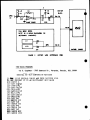
Figure 1 is a block diagram of the affected portions of the system when
Full BASIC is installed. Capacitor Ca is added to the GIANT BOARD because
the output of At2 (Pin 4) is normally low. Diode Db is a clamp on the output
signal during cassette read and maintains the proper de operating level.
The problem with this modification, is that it partially defeats the
purpose of the cassette read circuit (A12). This amplifier is intended to
"squa.re-up" the cassette signal, but capacitor Ca reduces the effectiveness
of this circuit. Diodes Da (GIANT BOARD), D1, and D3 (BASIC board)
comprise a "wired OR" so that the EF2 line may be shared.
AUTO-SWITCH CIRCUIT OPERATION
Figure 2 is a block diagram of the system where the Full BASIC GIANT BOARD
modifications are removed and the Auto-Switch modifications added to the
Full BASIC board. This circuit (Figure J) is essentially an automatic
switch that connects either the cassette read or the Full BASIC EF2 signals
to the buss. The basic circuit consists of four components; U1 CD 4066
(qua.d bi-lateral switch), R1, R2, and C1. R3 and the LED are optional.
6
AUTO-SWITCH CIRCUIT OPERATION oontinued
SW1 acts as a buffer for the Al2 GIANT BOARD EF2 signal. When a cassette
signal is present, Cl is charged to 5 volts which enables SWJ to put the
cassette signal on the buss. SW2 is...!!mply an inverter of the output
of SW1 and turns off the Full BASIC EF2 signals. (SW4). '!he optional LED
turns on when the cassette line takes control. When no cassette signal
!!...,present, sw4 is turned on, and the Full BASIC board has oontrol of the
EF2 line.
This modification eliminates the ac coupling of the cassette signal to the buss
allows a cassette read even when the Full BASIC board would be holding
EF2 low. It should be noted, however, that after the program is loaded,
it still may be necessary to enter "PR CIA" to resume normal operation of
Full BASIC. '!his is because the "WAD" routine does not reset the math chip.
~
This circuit does give priority to cassette operations and therefore the
cassette recorder should not be operated during Full BASIC program execution.
CONSTRUCTION DETAILS
The circuit shown in Figure J may be readily added to the Full BASIC
P.C. board in the area reserved for user hardware in the lower right hand
oorner of the board. '!he following modifications are necessary.
1) Remove the .1uf capacitor and the two diodes that were added to the
GIANT BOARD for Full BASIC.
2) Connect a wire from A12
Pin 4 (where the capacitor was) to Pin 84.
J) Connect a wire on the mother board between pins 84 of the GIANT
and Full BASIC board sockets.
4) On the Full BASIC board, cut the trace to Pin 70 after the junction
of Dl and DJ.
5) Wire up the Auto-Switch circuit as shown in Figure J.
6) The total system should now be wired as shown in Figure 2.
At this point, one note of caution is in order. If the Full BASIC board
is removed from the system, Pin 70 on the GIANT BOARD must be reoonneoted
for cassette read operation. I have been using Full BASIC with this
modification for several days now and have encountered no problems. As
long as one remembers that the cassette will take priority over the math
chip (as described earlier) there should be no problems. One interesting
side effect of this modification is that the LED acts as a cassette signal
present indicator, which is cute i f not functional.
7
~
>+5
< 1M
CASS.
IN
0-
r
~I ~ AA
u 2Ir
SYSTEM
1M
AAA_
rr
LEAVE CUT
PER NfTRONlc~
vv v
-
:A12
P1N4
1
X MOO
rADO JUI'?S\
-=- GIANT SOARD
SUSS
PIN 70
PIN &4
MOO
AOO
SUSSIVIRE
FULL eA51C ISQflRO
CASSo INPUT
SEE SCHEMATIc
FIGURE: .3
PlN84
V
PIN7C
m
1002
OUTPUT
FULL aASlC INPUT
AUTO - SWITt:Iof
I
I
lA
UI
N
Df
U 10
1_
N
D3
FIGURe 2.:
SYSTEM
~
X
CUT
'M'ITH
HERE
PIN 10
-EF2
AUTO - SWITGH 1'100
MoTHER
~D
8
CASS.
IN
CA
MOO
FULl IlUIC ~
(NOlt:OI 15 SMOII'N ~. . . ON
...
~.~)
lAl
UIO
TINY BASIC PROGRAMS
-by G. Caughman - 3795 Somerset Dr., Marqetta, Georgia, USA, 30064
DECntAL TO HEX COMVERS ION ROUTINE
1 0 " INPUT DECD-1AL VALUE AND THIS ROUTINE TiVILL
~O REM CONVERT IT TO AN EQUIVALENT HEX VALUE
100 INPUT X
110 LET Is-,/16
120 U-X-16*I
130 LET J&I/16
:1.140 TaI-16*J
150 LET K.:'J/16
160 !:J -16.l-K
170 LET L::K/16
180 RaK-16*L
400 LET V:=R
410 'OaUB 500
420 LET V::.!
430 GOaUB 500
440 LET VaT
450 GOS UB 500
~60 LET V=.U
UB $00.. "'
470 GOSUB 1000
tee Goa
•
500
IF V<lO ~GTO 570
IF J.:z10 PRINT "A";
IF V=ll PRINT "E";
IF Vz12 FRINT "C";
IF V:::13 PRINT "D";
IF V~14 PRINT "E";
IF V~15 PRINT "F";
RETURN
PRINT "V";
9
510
530
550
552
554
556
560
570
580 RETLTR~;
1000 PRINT
1010 END
10
20
30
40
50
55
60
65
70
TINY BASIC HEX TO DECDvlAL ROUTINE
LET k=10
LET Bs:rm
LET C2 1 2
LET D=13
LET E:.14
LET F:.15
PRINT "INPUT FOUR HEX DIGITS EACH FOLLOWED BY C0I<1:1AS";
PRINT "EXCEPT LAST DIGIT. (MAX. 7,F,F,F)"
INPUT U,T,V,W
.
~5 u~ U"~16"~16"~16
_
•
80
85
90
95
100
5
6
7
e
11
20
25
30
35
40
50
51
52
56
57
58
59
65
72
73
75
80
85
T#T*16*16
V=V"~16
X= U+-T+V+W
lRL'lT X
END
PRINT "MEr<lOR~ DISPLAYPROGRAM tI
PRINT
PRINT "ENTER THE STARTING ADDRESS AS FOLLOVIS: N,N,N,N.";
I'RINT "VvHERE N EQUALS EACH HEX DIGIT. (MAX 7,F,F,F)"
GO SUB 1010
LET Y= X
PRINT "ENTER LAST ADDRESS THE SAIJIE WP::l"
GO SUB 1010
LET Z::: X
REM CLEAR SCREEN AND SPACE
PLOT (12)
PRINT
LET X::. Y
GO SUB 110
LET W PEEK (Y)
Y"'Y+1
LET X=W
REM SET BYTE FLAG FOR HEX OUTPUT ROUTINE
LET p:s 1
GO SUB 110
IF Y < Z 1 THEN GO TO 56
END
=
+
10
100
110
120
130
140
150
160
170
180
400
402
410
420
430
434
435
440
450
460
465
466
470
475
500
510
530
550
552
554
REM HEX OUTPUT ROUTINE
LET I 1:1 JV16
U X -16
I
LET J:: I/16
To: I- 16*J
LET Kz J/16
B:2 J'-16*I
LET L: K/16
R:: K -16*L
LET V~R
IF P=l GOTO 435
GOSUB 500
LET V:.S
GOSUB 500
REM RESET BYTE FLAG IF SET
LET P:O
LET VaT
GOSUB 500
LET V=U
GOS UB 500
REM ALLOW TWO SPACES
. PRINT"
tt;
RETURN
IF V<10 GOTO 570
IF V:10 PR "A tt ;
IF V=ll PR "B";
IF V:12 PR "C tt ;
IF V:13 PR "D";
IF V.:14 PR liE";
556 IF V.:15 PR
560 RETURN
570 PRINT V;
580 : RETURN
1000 REM HEX TO DECIMAL ROUTINE
1010 LET A:10
1020 LET B=ll
1021 LET C-12
1022 LET D:.13
1023 LET E:14
1024 LET F~15
1030 INPUT U,T,V,W
1040 U-=U••16*16*16
1050 T.cT*16*16
1060 V~V*16
1070 Xt:U+T~V+W
1090 RETURN
=
*
"r",
11
THE MEGABYTE ELF
_ by R. Siddall - 40 Cadillac Ave., Downsview, Ontario, Canada, M3H 152
INTRODUCTION
UP TO NOW, FEW HOBBYISTS HAVE FOUND THE 64K ADDRESSIBILITY LIMIT OF THE
1802 TO BE MUCH OF A PROBLEM. TilE SITUATION MAY SOON CHANGE, HOWEVER. WITH
TilE APPEARENCE ON TilE MARKET OF 64K X 1 RAM CHIPS, AND THE CONSTANTLY
DECREASING COST OF OTHER LESS CAPACIOUS MEMORY CHIPS, IT MAY SOON BE
NECESSARY TO FIND A WAY TO EXPAND THE USABLE MEMORY SPACE. TO ADDRESS THE,
PROBLEM (IF YOU WILL PARDON THE PUN) I HAVE DEVISED A MEMORY MANAGEMENT
SCHEME THAT WOULD PERMIT AN 1802-BASED COMPUTER TO USE UP TO 1 MEGABYTE OF
MEMORY, IN 64K SEGMENTS. OTIIER BENEFITS OF MY SCHEME WOULD BE A MEMORY
PROTECTION CAPABILITY, AND AN ABILITY TO SEPARATE TilE PROGRAM SPACE FROM
THE ADDRESS SPACE.
THIS SYSTEM IS AT PRESENT MERELY 'THEORETICAL', BUT IT IS RELATIVELY
STRAIGHTFORWAIW, AND I IIOPE TO MAKE A BREADBOARD IMPLEMENTATION SOMEDAY. I
ALSO INVITE OTIIERS TO TRY IT OUT AND LET ME KNOW WHAT PROBLEMS I HAVE
FAILED TO FORSEE.
ACCESSING 1 MEGABYTE REQUIRES A 20 BIT ADDRESS, 4 BITS MORE THAN IS
PROVIDED BY THE 1802 ARCIIITECTURE. IN MY SCHEME, TWO 4-BIT 'NYBBLES' WOULD
BE LATCHED OFF THE DATA BUS BY AN I/O INSTRUCTION IN TilE PROGRAM BEING
EXECUTED. ONE OF THESE WOULD BE USED AS THE 'SEGMENT ADDRESS' (I.E.
ADDRESS BITS 17-20) WHENEVER THE PROGRAM COUNTER REGISTER IS BEING USED TO
ACCESS MEMORY: DURING TIlE FETCH CYCLE, AND WHENEVER AN 'IMMEDIATE' OR
BRANCH INSTRUCTION IS BEING EXECUTED. TIlE OTIIER SEGMENT ADDRESS IS USED
FOR ALL OTHER MEMORY ACCESSES INCLUDING DMA REQUESTS. TilE PROGRAMMER MAY
CHOOSE TO MAKE THESE TWO SEGMENT ADDRESSES POiNT TO TilE SAME SEGMENT, OR
HE CAN IIAVE A 64K PROGRAM SPACE AND A 64K DATA SPACE SIMULTANEOUSLY
ACCESSIBLE.
IIARDWARE
FIGURE I SHOWS THE HARDWARE REQUIRED. ICI IS A STANDARD 1852 I/O PORT
CONTROLLED BY AN 110 LINE FROM TilE CPU. IT IIOLDSONTO TilE SEGMENT
ADDRESSES SENT TO IT BY TIlE CPU WilEN TIlE APPROPRIATE OUTPUT INSTRUCTION IS
EXECUTED. AN RC CIRCUIT ON THE CLEAR PIN COULD BE USED TO SET BOTH SEGMENT
ADDRESSES TO 0 AT POWER ON.
IC2, Ica, AND IC4 CONSTITUTE A LOGICAL ARRAY WIIICII DISTINGUISHES
WHETHER AN INSTRUCTION BEING FETCHED ON THE DATA BUS WILL REQUIRE DATA TO
BE READ FROM TilE PROGRAM SPACE (I.E. VIA REGISTER P) OR THE DATA SPACE
(VIA REGISTER X OR ANY REGISTER OTIIER THAN P>. TilE TRUE/FALSE OUTPUT OF
TillS LOGICAL ARRAY IS IIELD AFTER A FETCII CYCLE IN ONE IIALF OF A 4013 DUAL
D LATcn r rcor. t CALL tHIS CIRCUIT (FIG. 2) TilE 'INSTRUCTION/DATA
DISCRIMINATOR' •
IC5 IS USED TO DISCRIMINATE BETWEEN A FETCII AND AN EXECUTE CYCLE. THE
OTHER HALF OF ICG PUTS OUT A TRUE/FALSE SIGNAL (AND ITS INVERSE) DEPENDING
12
ON WIliCH OF TilE SEGMENT ADDRESSES IS TO BE USED IN TilE SUBSEQUENT FETCH.
IC? IS A 4019 4 OF 8 SELECTOR WHICH PUTS OUT EITHER ONE OR THE OTIIER
SEGMENT ADDRESS FROM IC 1 DEPENDING ON THE OUTPUT OF IC6. IC8 IS A 4 TO 16
LINE DECODER WIIICII WILL SELECT TilE SEGMENT OF MEMORY REQUIRED.
I HAVE SPECIFIED CMOS ICS TIIROUGIIOUT THE CIRCUIT, BUT I FULLY REALIZE
THAT TIMING WILL PROBABLY BE A CRITICAL FACTOR, AND SOME OR ALL OF THE ItS
MAY IIAVE TO BE STTL OR EVEN EeL EQUIVALENTS TO THE ClIIPS INDICATED TO MAKE
THE SYSTEM WORK.
SOFTWARE
TilE 1852 I/O PORT WHICII 1I0LDS THE SEGMENT ADDRESSES CAN BE TIED TO ANY
AVAILABLE 110 LINE ON THE 1802. IN WHAT FOLLOWS I ASSUME IT IS TIED TO NO.
AN 'OUTl' (61) INSTRUCTION CAN THEN BE USED TO WRITE rna SEGMENT ADDRESSES
TO TillS PORT. TIlE IIIGII ORDER 4 BITS OF THE BYTE STORED IN THE PORT WOULD
CONTAIN TilE PROGRAM SEGMENT WHILE THE LOW ORDER 4 BITS WOULD CONTAIN THE
DATA SEGMENT.
TilE DATA SEGMENT CAN EASILY BE CHANGED AT ANY TIME UNDER PROGRAM
CONTROL. LISTING I GIVES A SMALL PROGRAM TIIAT WOULD COPY DATA FROM SEGMENT
1 TO SEGMENT 2.
CHANGING THE PROGRAM SEGMENT WOULD BE A LITTLE MORE DIFFICULT, SINCE
TilE PROGRAM COUNTER WOULD BE UNAFFECTED BY THE CHANGE OF SEGMENT ADDRESS.
FOR EXAMPLE, IF TilE 'OUTl' INSTRUCTION TIIAT CHANGED TilE SEGMENT ADDRESS
WERE AT LOCATION 001FO, AND TilE SEGMENT WERE CHANGED FROM 0 TO 2, THE NEXT
INSTRUCTION EXECUTED WOULD BE THE ONE AT LOCATION 201Fl. TO GET AROUND
TillS, A PROGRAM SEGMENT CIIANGE CONVENTION OF SOME KIND WOULD HAVE TO BE
SET UP. MY SUGGESTION IS TIIAT EVERY SEGMENT USED AS A PROGRAM SEGMENT IIAVE
A 'SEP RO' INSTRUCTION IN LOCATION 0000 AND AN 'OUTl' INSTRUCTION IN
LOCATION FFFF (TillS COULD BE IMPLEMENTED IN HARDWARE). TUEN, TO CHANGE
PROGIMM SEGMENTS, THE PROCEDURE WOULD BE AS FOLLOWS:
-SWITCII TIlE PC TO A REGISTER OTHER TIIAN RO,
-POINT TilE X-REGISTER TO A BYTE CONTAINING TilE TWO NEW SEGMENT
ADDRESSES,
-POINT REGISTER RO TO TilE ENTRY POINT OF TilE PROGRAM TO BE EXECUTED IN
THE NEW SEGMENT,
-BRANCH TO LOCATION FFFF.
CONTROL WOULD THEN JUMP TO rna 'OUTl' INSTRIlCTION AT LOCATION FFFF, TIlE
SEGMENT WOULD CIIANGE. TilE NEXT INSTRUCTION EXECUTEI) WOULD BE THE 'SEP RO'
INSTltUCTION AT LOCATION 0000 OF rna NEW SEGMENT, CAUSING A BRANCH TO THE
DESIRED PROGRAM.
TO TAKE ADVANTAGE OF THE SEPARATE ADDRESS SPACE, SPECIAL ASSEMBLER AND
BASIC SOFTWAlm WOULD IIAVE TO BE DEVELOPED. FOR EXAMPLE, ADDRESS LABELS
WOULD HAVE TO BE MARKED SOMEHOW AS TO WHETHER THEY wEim ADDRESSES IN TilE
PROGRAM OR DATA SPACE. EXISTING SOFTWARE WOULD STILL RUN, BUT IT WOULD BE
CONFINED TO TIlE USUAL 64K.
13
•
MEMORY PROTECTION
INIIERENT IN TillS SCIIEME IS A USEFUL FORM OF MEMORY PROTECTION. IF THE
PROGRAM AND DATA SEGMENTS ARE DIFFERENT, IT IS IMPOSSIBLE FOR TilE PROGRAM
TO BE CLOnBElmDBY A STRAY DATA POINTER OR FOR TilE SYSTEM TO ATTEMPT TO
EXECUTE DATA. FURTIIERMORE, DATA IN SEGMENTS OTIIER TIIAN THE TWO ACTIVE ONES
CANNOT BE ACCESSED AT ALL, UNLESS AN ERRONEOUS 'OUT l' INSTRUCTION IS
EXECUTED.
FRONT PANEL FUNCTIONS
WITH A BIT OF ADDITIONAL HARDWARE, A FEW USEFUL FRONT PANEL FEATURES
COULD BE ADDED. FOR EXAMPLE
-TilE OUTPUT OF IC6 COULD BE USED TO LATCH OUT THE CURRENT TRUE PROGRAM
COUNTER FROM TilE ADDRESS LINES.
-THE ACTIVE SEGMENT ADDRESS(ES) COULD BE DISPLAYED ON TilE FRONT PANEL.
-TilE PROGRAM AND DATA SEGMENTS COULD BE CONTROLLED FROM THE FRONT
PANEL BY OVERRIDING TilE OUTPUT OF IC7.
OTIIER CONSIDERATIONS
OF COURSE, IT WOULD NOT BE NECESSARY TO ACTUALLY HAVE A MEGABYTE OF
STORAGE, OR EVEN 64K, TO 'fAKE ADVANTAGE OF THIS SCHEME. IN rns SYSTEM I
ENVISAGE, SEGMENT 0 WOULD CONSIST ENTIRELY OF ROM, AND WOULD CONTAIN THE
OPERATING SYSTEM (STARTUP PROGRAMS, MONITOR, INTERPRETERS, MATHEMATICAL
SUBROUTINES, ETC.). SEGMENT 1 WOULD BE RAM, BUT PART OF IT WOULD BE
RESERVED FOR USE BY TilE OPERATING SYSTEM TO STORE DATA, MAINTAIN STACKS,
PASS PARMETERS, ETC. SEGMENTS 3 TO F WOULD BE AVAILABLE TO THE USER. IF
NOT USED FOR MEMORY, ONE OR MORE OF THE SEGMENTS COULD BE USED FOR
MEMORY-MAPPED I/O. SOME OF THE SEGMENTS COULD BE MISSING ALTOGETHER OR
COULD CONTAIN LESS THAN 64K. IT WOULD, OF COURSE, BE UP TO TilE USER TO
REMEMBER WHERE TilE HOLES ARE IN lIIS ADDRESS SPACE.
ONE IDEA THAT INTRIGUES ME IS TO HAVE A 64K APL INTERPRETER IN SEGMENT
0, WITH THE OTHER 15 SEGMENTS AVAILABLE AS APL WORKSPACES. (APL IS MY
FAVOURITE LANGUAGE.)
IT WOULD BE NICE IF RCA (OR SOME ENTERPRISING SECOND-SOURCER) CAME OUT
WITH A ONE-CIIIP CMOS IC CONTAINING TilE ABOVE CIRCUITRY, WITHOUT TilE 4515,
BUT INCLUDING A LATCII TO TAKE OFF TIlE UPPER ADDRESS BYTE. THE WHOLE TIlING
COULD BE DONE IN A SINGLE 40 PIN IC. WHICH WOULD ADD A LOT OF POWER TO THE
1802 SERIES, AND ALSO MAKE LIFE EASIER FOR us JlOMEBREWERS.
14
•
teo
I
.....---+---------------- ..
I
DATA
f>U"
04
01
..••
Ica
.eoo.a
IC4
4..,
IC" ".5
15
CONCLUSION
AS I SAID EARLIER, TillS WHOLE SCHEME IS JUST THEORY AT THE MOMENT.
UNFORTUNATELY I AM NOT VERY WELL EQUIPPED FOR THE AMOUNT OF BREADBOARDING
THAT TillS SYSTEM WOULD ENTAIL. I WELCOME ANYONE ELSE TO TRY IT OUT AND
SEND ME ANY COMMENTS THEY MAY HAVE.
LISTING I - SAMPLE PROGRAM TO COpy DATA BETWEEN SEGMENTS
*********************************************************
* THIS PROGRAM COPIES DATA FROM SEGMENT 1 TO SEGMENT 2.
*
*
*
*
*
*
*
LOOP
R8
R9
RA
RB
RC
-
STACK POINTER FOR DATA SEGMENT 1
STACK POINTER FOR DATA SEGMENT 2
CONTAINS START ADDRESS OF DATA IN SEGMENT 1
CONTAINS DESTINATION ADDRESS IN SEGMENT 2
CONTAINS NUMBER OF BYTES TO BE COPIED
SEX
LDI
STR
OUTl
DEC
SEX
LDI
STR
OUTl
DEC
LDR
SEX
OUTl
DEC
STR
SEX
OUTl
DEC
INC
INC
DEC
GLO
BNZ
Gill
BNZ
*END
R8
-X02
R8
R8
R9
-XOI
R9
R9
RA
R8
SEGMENT POINTER P-O D-2
SAVE ON STACK IN SEGMENT 1
SWITCH DATA SEGMENT TO 2
SEGMENT POINTER P-O D-l
SAVE ON STACK IN SEGMENT 2
SWITCH DATA SEGMENT BACK TO 1
GET BYTE TO BE COPIED
SWITCH DATA SEGMENT TO 2
R8
RB
R9
STORE IN DATA SEGMENT 2
SWITCH DATA SEGMENT TO 1
R9
RA
RB
RC
RC
LOOP
RC
LOOP
BRANCH BACK UNTIL RC IS ZERO
16
•
HEXKEYBOARD FOR THE ELF
-~
Here is another simple keyboard that will replace the data
switches on the original ELF. The original circuit was taken
from ETI Magazine (September 77, pa o60) and modified to hold
the data into two latches. The circuit uses TTL chips because
they were handy and cost me almost nothing.
The circuit could
be modified to use CMOS or LSTTL. The keypad comes from a surplus calculator keyboard bought from Rdio Shack.
fied to make it a 16 spst
common o
It was modi-
switches arrangement with one. side
This was done by cutting the printed circuit and re-
wiring the sWitches. There are various surplus keyboard on the
market and it should be easy to do the same with any keyboard
providing you have accessto the switches or the printed circuit.
Most keyboard are 'matrix' type so they have to be modified
to work in this circuit. 16 spst sWitches could also .be used
(push button type). Use Ie socket for your circuit. The control
circuit was built on a small phenolic board and screwed under
the keypad with 12 wires coming out. ( 8 data, +5v, grd, strobe,
enter).
The extra switch
ELF I call it ENTER.
replac~
A led
the IN switch in the original·
(kbd ready) indicates the circuit
is ready to accept another byte. When the second digit is pressed
a data ready strobe is generated and inverted to drive an EF
line on the 1802.
I am including a short program that will
input data in memory sequencely, it uses EF2 for input strobe.
17
t:
:::s
V
c
G
~
0
a:
!v
.-
~~
~
w
::.:::
0
X
~
lJJ
0
V
CIA
~
•
II)
l\o.
.
1ft
~
f')
(\I
0
.,
ri~
i!
~
W
•
00-
Z
>
1ft
+
+tV
47 t<
MTA MtDr
~TA
'I'D
READY
~
U
I~SfON
LIM
II
cI)
18
1802 TO S-lOO BUS CONVERTER
- by David W. Schuler, 3032 Avon Road, Bethlehem, Pa. 18017, U.S.A.
Theory of Operation:
Bus buffer Ul is used to buffer the data 1i nes from the 1802. Si nce the
S-lOO bus has separate data in/out lines, the chip select of the buffer is
always enabled (pins 1 and 19 = 0). U2 is used to strobe the data from the
S-lOO bus onto the 1802 bi -di rect i ona1 data bus when a memory read is
requested. The chip select of U2 is generated by U3a and U4a on the Elf II
only. On the Elf II, pin 1 of U4a is connected to pin 69 of the 86 pin bus
on the main board. This line indicates if an on-board memory address has
been selected. If pin 69 = 0, the S-lOO buffer is disabled. If pin 69 =
1, the S-lOO bus buffer is enabled when a memory read request is received.
The Netronics Elf II also requires a latch for the upper 8 address bits (A8
to A15). The required circuit is in Figure 3. This will latch the 8 high
order addr. bits, and then the lower 8 address bits. This is because the
S-lOO board specifications require that the full 16 bit address be present
on the bus at the same time.
For both the Quest Super Elf and the Netronics Super Elf, U3a, U3b, and U3c
are required to invert the 1802 signals to the required S-lOO signals.
Construction:
The entire ci rcuit can be bui It on one S-lOO interface card by either wi re
wrappi ng or poi nt-to-poi nt connections.· If the Super Elf or the Elf II
wi th Quest Adapter board is used, only a 50 conductor cable and S-lOO
prototypi ng card are needed. If only an El f I lis used, a Kl udge Card for
the 86 pin bus, an S-lOO prototyping card and appropriate cable will be
required. In either case, a S-lOO mother board will be required.
El f II Note:
In some cases, transistor Ql on all 4K Static RAM cards will have to be
replaced with a higher speed transistor. Al so, sometimes diode D4 on the
Giant Board will have to be replaced with a higher speed germanium diode.
If there are any questions or comments on the interface outlined here,
please send a SASE (Self Addressed Stamped Enveloped) along with your
questions and I will try to help you out.
19
FIGURE 1
8-100
cormect
(Pin I)
(Signal name)
1
2
20
25
29
30
31
32
33
J4
35
36
37
J8
39
+8VDC
+16VDC
GND
pSTVAL
A5
A4
.A.3
.A.15
A12
A9
oot
oo~
Al_
D04
005
006
DI2
DI3
DI7
sOUT
sINP
40
41
42
43
45
46
47
50
51
52
68
70
77
79
80
81
82
83
sMEMR
GND
+8VDC
-16VDC
MWRT
GND
~
Al
A2
A6
A7
84
A.8
85
86
87
A13
A14
A11
D02
003
007
DI4
DI5
DI6
DIl
DI_
POC
GND
88
89
90
91
92
93
~
95
99
100
Notes I
1 - Elf' II
1802
to
(Signalname)
"
"
"
"
"
"
"
"
"
"
"
"
"
"
"
"
"
"
"
"
"
"
"
"
"
"
"
"
"
"
".
"..
.."
"
"
"
"
"
"
"
"
II
"
II
-
m
A5
A4
A3
A15
A12
A9
001
00_
Al_
D04
D05
006
DI2
DI3
DI7
GND
GND
(Note
(Note
(Note
(Note
(Note
(Note
(Note
(Note
(Note
(Note
(Note
(Note
(Note
3)
(Note
3)
GND
-
iiiR
A_
.A.1
.A.2
A6
A7
A8
A13
A14
All
002
003
(Note 1)
(Note 1)
(Note 1)
(Note 1)
(Note 2)
(Note 2)
DC1l (Note 2)
DI4 (Note 2)
DI5 (Note 2)
DI6 (Note 2~
DIl (Note 2
DI_ (Note 2)
(Note 3)
GND
only I See Figure :3 tor latch
c1rcuit tor Address lines A.8 to A15.
2 - All I See Figure 2 tor da:ta latch.
All' See Figure 2 tor cirauit data•
. - other 8-100 lines may have to be added
as required by irxlividual boards.
Z- -
1)
1)
1)
2)
2)
1)
2)
2)
2)
2)
2)
2)
-:>
20
, I !it U'R.E
z
N
J
":'
~
c+ :
ct 7
r=-. :
Po
rl
P
/'1\
p.
~
~
~
ri
~
...p
~
r-
itS
35
., ~'i
'lit
~"
'4.
~@
'iii
Ii
t"
II
V\
J
\I>
1&
~'2,
II
~::
~ II;
~
~
•
,,,
'&.
'e...
·U
-
'&..
'3'
~!'1
I
U
1/\
"to
0
'It
I-
90
p
'i3
'i1
M-')
10
11&
~
••
V')c.
~
R/W
(Q~ Ol'\ly)
II - ~ll.st - COf\ned to tS"
Sb pin bu~
Ne+ronic.c; - Pi", ,,~
"
If'
t
8
",
'i
a
Iii
AI
7
10
'1'1
A).
13
II
Jl
A'
1'1
IJ)
:>
~!>
I"
~
~
HV
~
'&.
.,
I
'&
T
T?"
fi
,
-s
",
\}!.
iL
M
II>
0
I-
,~
It)
~
,~
10
IS
'I
II»
;)
Aft
11
A1
1'1
,
e
1
'l>04'R. ,'S
U I. U2,
L I ~T
ell..$'IiO /.,
u3
.,..,I-S9I'1
Uli
VS,UD
1~L.S¢~
'10"':.l..
I
1/\
l'Jr
'i$"o~
31
21
.
ANOTABLE ASSEMBLER LOADER
_ by D. Stevens, 4 Washington Sq. Village, #13R, N.Y., N.Y., USA, 10012
~nis routine allows one to assemble long object files without
using tape or disk; it can produce an object file with length a
RAM/3. I wrote it because I am tired of hand assembling my codes
and do not have a terminal or an assembler, just an ELF-II with
8 K RAM. The source (which is machine code + address instructions) is usually less than twice as long as the assembled object
file. The routine fits in 3 pages and runs slowly, needing for
instance 20 seconds to process its own source (5 pages) and
needing 200 seconds to process my operating system (source a 15
pages, object length = 08AO). It requires only 3 pages because it
keeps no tables. It will run much faster and can be used as a
loader if just the high address bytes are computed.
The source for the assembler has no mnemonics, only op codes
and address data. The address da.ta is given in strings of bytes
all beginning with 68. For example, the address of a particular
op code is given the name "AB" by preceeding the op code with
"68 61 AB", it is given the name "CD EF" by preceeding it with
"68 62 CD EF". In the source file, a short branch to these
locations would be "30 68 11 AB" and "30 68 12 CD EF". When the
assembler encounters a data form such as is in the left column
below it performs the action described in the right column. Now
look at the source listing of the assembler. The first two bytes
tell the assembler to write the object code starting at 1000, the
68 03 01 00 tells the assembler that the load address of the
object code is 01 00.
The next data up to 0417 is op codes,
compare with the object code listing.
At 0418 is 68 22 01 26,
then more op codes.
At 0112 in the object listing the byte 03
occurs instead.
The name "01 26" is defined at 0823 (the
68 62 01 26) and the address of the following byte is 035D.
Da ta String
Compiler Action
68 00
A "68" will be inserted in the object code.
68 01 xx yy
The address of the next byte in the object
code will be the address of the last byte
in the object code plus xx yy. This is a
SKIP instruction to the compiler.
68 02 xx yy
The low byte of the address of the next byte
in the object code will be yy. The high byte
will be the high byte of the last byte plus xx.
68 03 xx yy
The address of the next byte in the object code
will be xx yy This is an ORG instruction to
to the compiler.
22
.
68 1j (j bytes)
The low byte of the address associated with the
name will be inserted.
68 2j (j bytes)
The high byte of the address associated with
the name will be inserted.
68 3j (j bytes)
The high and low bytes of the address associated
with the name will be inserted.
68 4j (j bytes)
A preprocessor changes the source file as
follows: if the current object address is on
the same page as the address of the name
the 4j will be changed to 1j and the byte
preceeding the 68 will be changed from xy
to 3y. Oherwise the 4j will be changed to
3j and the byte preceeding the 68 will be
changed to Cy.
68 6j (j bytes)
The name is associated with the address of the'
next byte of the object code. The name is a
statement label.
68 7j(j bytes)hh11 The name refers to address hh11. This
is an EQUATE instruction to the compiler.
The routine is used as follows. It is assumed that your
system uses SCRT. The assembler object code is put at 0100-0308.
R8 should point to the low address end of a RAM area, the
assembler will store useful data, described below.
R9 should
point to the start of a source file, and RA should point to the
end of the file. The last byte in the file should not be part of
a 68...
address specifier; if it is, add a 00 to the end of your
source. Note the 00 at the end of the source listing of the
assembler.
The source should start with uu vv 68 03 xx yy, where
uu vv is the memory location where the object code will be put by
the assembler and xx yy is the load address where the code will
run. The assembler output should not overwrite the source.
During assembly the high address byte of the source byte being
processed is displayed. On return only registers R8, R9, RA and
RF a re changed. R9 noe has uu vv and RA points to the end of the
object code just generated.
The source is modified; 68 4J
patterns are changed to 68 lJ or to 68 3J patterns.
If a 68 1j ••••• combination occurs and the referenced address is on a different page, the assembled program possibly will
not be ok. Soa list of all such questionable references is made
with R8 the stack pointer.
This stack grows upward.
If for
instance on entry R8 was 1400 and on exit R8 was 1404, then [1400]
[1401] is the address in the source of a questionable combination,
and also [1402] [1403]. Entries are also made if a 68 3j •••••
combination refers to an address which is on the same page.
The routifte at 0327 - 0337 puts out the object bytes (the SF
instruction).
This may be modified to fill a buffer and write to
tape or disk rather than to memory.
23
If an error in the source data is detected the prosraa
branches to COOO. This error branch address can be changed, it is
at 036C in the object code in the listing and at 0842 in the
source part of the listing. The routine at COOO (or wherever)
should save R3, R9, and RB. The error table below lists the
possible error conditions.
Error Table
R3
Diagnosis
019B
01AE
01BO
0227
0281
02C6
0305
illegal data at RB
a "4j" in the source was not changed , is the source in ROM?
illegal data at RB
illegal data at RB-1
RB points to the last byte of a name which wsn' t found
illegal data at R9
illegal data at R9-1
Summa ry of Usage
1. Set up the source file
a. First five bytes are uu vv 68 xx yy
b. No mne1'lOmcs
c. Final byte not compiler instruction (68 •••••• )
2. Put the assembler at 0100
3. Put an error handling routine at COOO (or an address you pick)
4. Set up R8, R9 and RA
5. Do SCRT call to 0100
6. If the routine exits to the error routine use the table above
7. If the routine makes a normal exit, check R8 and the data in
the R8 stack.
Listing of Assembler Object Code
0100
0110
0120
0130
0140
0150
0160
0170
0180
0190
OlAO
01BO
01CO
01DO
OlEO
01FO
0200
0210
0220
0230
0240
E2 8E 73 9E
B7 F8 03 'BE
FO 68 FF 02
47 BA BB BC
42 BA 02 AA
5C 2C 2C OC
2C OC FA OF
19 E9 OB F7
8A F3 3A 8A
FB 68 3A BE
FE FC A4 A3
30 F9 OB FA
D4 03 27 30
4A 9D E7 F3
30 BF 9B 58
18 18 47 B5
8F AA DE 08
A7 42 BE 02
3D FF 01 32
8D F4 AD 2B
F4 BD OB AD
73
F8
D4
07
D4
FA
F9
AC
9B
1B
30
OF
7D
32
18
D4
29
AE
46
4B
30
87
5D
03
AA
02
OF
30
2B
52
OB
C5
FC
CO
D8
8B
03
09
D5
DE
52
3A
73
AE
8C
AB
4A
F9
5C
29
9A
FE
30
02
02
18
58
27
AF
4B
00
9D
4B
97
DE
17
AC
E7
CO
30
OB
F3
3B
C8
1B
16
18
28
30
29
32
F8
74
BD
73 82
04 19
07 32
1B 1C
9D F3
5C 30
1B 99
77 BC
32 FE
9B DE
30 DC
FF 01
9B 58
17 07
D4 02
D9 OB
09 B9
27 FF
68 2B
BD 2D
30 42
FF 24
19 D4
69 8A
D4 02
17 32
1B DC
BB 89
1B 29
1B 9B
00 F6
30 E2
3A B7
18 8B
30 BF
4A 9D
FA OF
8F A9
01 32
CO 01
CO 01
DE 01
A7 92
03 38
73 9A
A2 47
5B OC
FB 50
AB 2B
29 8B
52 64
F6 F6
DE 00
30 7D
58 28
D4 02
E7 F3
30 B7
12 42
2D FF
BF 1B
7D 4B
OB FA
7F 00
05 40
73 17
BD 12
FB 70
5C 2C
19 19
52 E2
22 OB
F6 F6
DE 00
OB B5
D4 02
4A 47
3A F2
9F BA
B7 42
01 32
OB 52
52 9D
OF A8
24
0250
0260
0270
0280
0290
02A0
02BO
02CO
02DO
02E0
02F0
0300
0310
0320
0330
0340
0350
0360
0370
0380
0390
03AO
03BO
03C0
03DO
B8 1B FF 01
73 28 88 3A
FF 73 98 FC
00 47 BA 07
02 D5 98 1A
30 8F DE 01
88 57 27 98
09 FE 3B C6
FO 30 ED 30
FA OF 19 FF
49 C2 03 05
C2 03 23 DE
49 19 52 98
CO 02 A4 49
BF 95 SF 94
3B D5 8D 73
SA 73 9A 73
33 50 F6 33
B8 42 A8 42
42 AB 42 BC
17 07 BB AB
E7 99 BC 89
2B 8B 3A A9
D5 E2 99 52
C8 2B 8B 32
3A 51 9B
SA 98 F9
02 73 D4
AA 1A OA
FF 01 3A
89 52 8A
57 DE 02
DE 00 F6
ED 30 EC
01 3A E2
FF 01 C2
00 18 CO
74 B8 28
B8 30 IE
B5 1D 9F
9D 73 8C
89 73 99
6E F6 33
69 42 A9
42 AC 42
97 B8 87
AC 98 B7
89 73 99
9A F3 32
BA 17 17
0400
0410
0420
0430
0440
0450
0460
0470
0480
0490
04A0
04BO
04C0
04DO
04EO
04FO
0500
0510
0520
0530
0540
0550
0560
0570
0580
0590
SAO
05BO
11
FF
01
68
17
07
02
OC
E1
5C
19
00
32
68
00
A3
68
00
12
EA
CO
68
00
EF
9B
12
30
E8
01
7F
62
05
12
1B
32
2C
E2
00
F7
E2
F3
12
E6
E7
30
OF
68
32
F4
9D
62
01
58
18
EE
F3
o
00
24
26
32
07
AA
AA
FB
68
30
19
E4
68
00
68
68
12
F2
00
B5
68
32
ED
04
58
00
68
68
68
A7
AE
01
32
AB
D4
70
62
68
E9
8B
12
3A
62
62
00
OB
E8
D4
32
01
17
68
18
F1
12
62
03
92
68
20
68
AC
68
5C
00
12
OB
52
00
68
00
00
EF
FA
30
68
00
00
68
32
8B
18
00
00
00
00
00
40
00
1C
01
2C
OC
E1
AC
8A
68
00
F6
30
68
FC
12
01
68
E7
00
00
28
68
68
9F
E2
B7
EO
FO
E3
D4
00
OC
FB
68
2B
F3
62
E9
F6
68
12
02
00
IF
62
F3
EE
47
D4
62
62
BF
60
03
FA
93
F3
D5
F6
30
30
03
02
30
8D
D5
73
73
42
42
BD
A8
88
73
CB
30
8E
F8
DE
68
8A
68
E7
FA
50
62
29
3A
00
1B
F6
12
00
68
E4
30
00
32
07
30
68
00
00
BA. 8F
8B AF OF 2F
73 F8 EF 73
8C 17 47 FB
10 3A 92 2A
1A 1A E7 OA
3A B8 99 52
49 FB 68 32
F6 F6 F6 FE
EC DE 00 30
A4 49 30 EO
09 FF 01 C2
A4 19 09 52
20 49 52 98
52 8C F4 AF
46 AF E7 46
9C 73 8B 73
88 73 98 73
F6 33 7D CO
BA 02 AA 30
02 AD 30 5C
1A 2B 2A 8B
A7 4C 17 F2
F8 55 57 27
19 30 9E 89
D1
E7 73 F8 FF
F8 68 73 F8
55 :32 81 DE
D4 02 A2 DE
73 2A OA 57
9A F3 3A B8
CO 18 30 A4
FC CF A3 30
E9 49 19 19
18 18 30 E9
03 19 FF 01
88 F4 A8 29
F4 B8 49 A8
9D 52 9C 74
73 2F 8F 3A
9B 73 30 5C
D3 43 E2 F6
CO 00 12 42
5C 12 42 BB
DE 01 DE 04
3A 99 9B AB
17 F3 3A C1
DE 08 DE 02
52 8A F33A
73
68
04
00
73
32
9D
OF
5C
00
OB
68
E5
OB
F6
00
FO
62
68
68
EC
68
30
68
32
F1
F2
AA
73
BE
62
68
47
BD
68
30
FA
89
29
9B
64
12
68
12
00
FF
OB
68
8B
18
EA
68
E7
68
30
09
9E
22
19
FF
9A
01
F3
F9
2C
E3
77
12
1B
FE
F6
EB
DE
00
62
12
9B
12
68
12
01
47
OB
DE
73
01
19
02
73
OA
17
CO
2C
99
BC
00
9B
3B
FE
30
00
E8
00
00
58
00
12
00
00
B5
FA
08
87
26
68
D4
17
47
32
5C
OC
BB
1B
E5
52
68
FC
68
DE
1B
E9
E4
18
ED
00
EA
9D
D4
OF
29
97
F8
00
32
BA
12
12
68
OF
AB
29
52
22
00
12
00
30
01
68
62
58
18
68
62
F3
32
68
AF
73
68
E1
00
BB
42
00
12
F9
2B
68
9A
OB
E6
00
EC
68
3A
62
00
28
68
62
00
3A
01
12
29
82
12
D4
DO
BC
BA
E2
00
30
19
62
F3
FB
DE
E7
30
12
68
00
EB
D4
62
00
FO
68
IF
00
09
25
OSCO
05DO
OSEO
05FO
0600
0610
0620
0630
0640
0650
0660
0670
0680
0690
06A0
06BO
06C0
06DO
06E0
06FO
0700
0710
0720
0730
0740
0750
0760
0770
0780
0790
07AO
07BO
07CO
07D0
07E0
07F0
0800
0810
0820
0830
0840
0850
0860
0870
0880
0890
OBAO
08BO
08C0
0800
OBEO
08FO
B9 8F A9 12
F4 4B 32 68
32 68 12 00
00 F5 F8 68
OB 52
F4
CO 68 32 00
00 F9 OB AD
68 12 00 F9
62 01 01 1B
62 01 02 OF
02 98 F9 60
FC 02 73 D4
03 DE 00 68
68 12 01 05
D5 68 62 01
01 06 1A 1A
62 01 OA DE
01 OC 99 52
DE 02 D5 68
18 30 68 12
(E DE 00 68
01 OF A3 68
14 30 68 12
DE 00 30 68
68 62 01 11
OB 68 62 01
68 62 01 14
68 32 01 16
01 18 FF 01
CO 68 32 01
49 19 52 98
49 52 98 F4
68 32 01 OB
62 01 1F
B5 1D 9F D5
73 2F 8F 3A
73 8C 73 9C
01 24 8A 73
01 25 D3 68
33 68 12 01
28 CO CO 00
A9 42 BA 02
BB 42 AB 42
68 62 00 DO
97 B8 87 A8
D2 68 62 00
68 62 00 D4
3A 68 12 00
27 DE 08 DE
68 12 00 D8
00 DB 89 52
8B 32 68 12
an
an
42 B7
12 00
F8 FF
00 2B
AD 2B
E4 68
30 68
68 62
FF 01
2F E7
73 F8
68 32
62 01
2A D4
05 98
E7 OA
01 68
9A F3
62 01
01 OB
62 01
62 01
01 14
12 01
19 FF
12 49
18 30
FF 01
C2 68
OB 68
74 B8
B8 68
68 62
52 8C
68 62
68 12
73 8B
9A 73
62 01
27 F6
68 62
AA 30
BC 42
DE 01
1A 68
D3 9B
4C 17
D4 89
02 D5
68 62
8A F3
00 D5
42 A7
F5 FF
01 32
CO 68
4B 52
62 00
12 00
01 00
3A 68
73 F8
EF 73
00 DO
03 47
68 32
68 62
73 2A
62 01
3A 68
OC 49
68 62
OE F6
OF 30
30 68
12 49
01 3A
30 68
68 12
C2 68
32 01
62 01
28 30
62 01
01 1B
F4 AF
01 20
01 21
73 9B
89 73
26 43
33 68
01 27
68 12
AC 42
DE 04
62 00
AB E7
F2 17
73 99
68 62
00 D7
3A 68
17 17
42 BE 02 AE
01 32 68 12
68 12 00 FA
32 00 EA 68
9D 74 BD 2D
F8 4B 52 9D
F7 68 62 00
DE 01 OB FA
12 01 01 9B
FF 73 28 88
F8 68 00 73
17 47 FB 55
BA 07 AA 1A
01 OA 68 62
01 06 1A FF
OA 57 30 68
OB 89 52 8A
12 01 OC 88
FB 68 00 32
01 OD 09 FE
F6 F6 F6 F6
68 12 01 15
12 01 13 30
19 19 68 62
68 12 01 11
12 01 10 68
01 12 68 62
320117FF
1B DE 00 68
17 19 09 52
68 12 01 1A
19 49 A8 68
49 B8 30 68
9D 52 9C 74
46 AF E7 68
D5 68 62 01
73 30 68 12
99 73 88 73
E2 F6 33 68
12 01 23 F6
12 42 B8 42
01 25 68 62
BD 02 AD 30
17 07 68 62
D2 2B 2A 8B
99 BC 89 AC
F3 3A 68 12
73 F8 55 68
00 D6 E2 99
19 30 68 12
12 00 D7 68
30 68 12 00
D5 68 62 00
00 F6 FF 01
DE 00 68 62
62 00 F6 1B
68 62 00 F7
F4 BD 68 62
FA 4B BD 30
OF A8 B8 68
BF 8B AF 68
3A 68 12 01
F8 FF 73 98
32 68 12 01
OA FA 10 3A
01 04 DE 02
01 3A 68 12
12 01 04 68
F3 3A 68 12
57 27 98 57
68 12 01 OD
3B 68 12 01
FE FC 68 12
30 68 12 01
68 12 01 13
01 10 FA OF
30 68 12 01
62011318
01 15 49 C2
01 C2 68 32
62 01 16 18
88 F4 A8 29
68 62 01 18
62 01 1A CO
12 01 19 68
BF 95 5F 94
62 01 21 46
23 8D 73 9D
01 25 68 62
98 73 68 62
12 01 24 F6
33 68 12 01
A8 42 B9 42
01 28 12 42
68 12 01 25
00 D1 BB AB
3A 68 12 00
98 B7 88 A7
00 D6 2B 8B
62 00 D5 57
52 9A F3 32
00 D3 68 62
62 00 D9 2B
D9 00
26
A HARDWARE CLOCK FOR THE 1802
_ by J. swofford, 2302 N. Fairview Ave. Decater, Illinois, USA, 62526
Lalt apring I ordered an OKI real-time olook/oalendar to till a
need for time-keeping in my RLF II. My oirouit built around thia
I.C. is memory-mapped via 8255 PPI and allows aooeaa to time in
hours, minutea and seoondl and the date al well al the day-otweek. Time oan be kept in either a 12 or 24 hour tormat and leap
year oompenaation il provided. My aystem has the 8255 looated
at FFOOH to FF03H. Unfortunately, the Netronioa monitor interterea with looationa beyond FDFFH, ao some ELF II ownera may wilh
to looate the 8255 elsewhere or, as I did, enable the Netronioa
monitor only tor FOOOH to FOFFH (aa it should have been, anyway).
INTERFACING THi CLOCK
The data sheet trom OKI showa a auggelted arrangement using the
Intel 8255 PPI. Sinoe I already had a tew aparea, it seemed the
eaaiest route to take. The oapabilities ot the PPI are too extensive to oover here 10 I will be oonoerned with only thoae aapeots
whioh arteot this applioation. Memory looationa FPOOH to PF03H
will be aaaum.d. All three ot the 8255 I/O porta are u.ed. The
PPI operate. here in mode 0 in two oonfigurations; one to read
trom the olook and one to write to the
1102...
&1S5
olook (aee figure 1). Theae atatea are
.~A
oreated by writing 80H into looation }
.us "'--~ A I'\r--"'"
PF03H tor olook WRITE and 90H for olock
Mii~--4I
8 ~_-,/,
~~-----4111
RBAD. Theae byte. oontrol hOW the 8255
itselt operates. An 80H will allow port
A to be an output port (ports Band C
remain output ports tor both olook READ
and olook WRITE). Similarly, 90H allows
port A to input the data nibble trom ,the
olook data linea. Port B is uaed to proPIGURB 1
vide the olook addrea. nibble and port C
ia tor olook oontrol (aee table 1). Vhen the 8255 ia reset, all
24 bits (th~e 8 bit porta) normally float. In thia oirouit, R1R16 will pull theae linea high. Thia would normally plaoe the olook
in a HOLD Itata, atopping the ttme inorement. Theretore, POO
(bit O-port 0) 1s inverted betore going to the ohip .eleot pin
on the olook. Thia removea all oontrol (inoluding HOLD) trom the
•
ct
clock and allows it to continue keeping time. Th. upp.r portion.
ot port. A and B (PA4-7 and P~-7) are not u.ed. P.14-7 i. tied
to ground through 10K re.istorl to avoid having to '.trip' th.m
ott in .ottware during clock READ •
.lDDRBSSING
Since I use other 8255. in my .ystem, the .chematic .how. a 74LS154
providing CS tor the clock'. 8255. U.ing this arrangement, 16
ditferent PPI. can be .elected yielding 48 8-bit I/O port.. Many
good method. ot high order addr.s. latching and chip ••lection
have appeared in Ip.o Facto. Thi. one work. tor me. Since you
may not have an interest in this expan.ion iel.a, you may wi.h to
use an alternate method of chip .el.ct which eliminate. the 74LS30,
74LS32, 74LS154 and 74LS374 (tigure 2). Out the trac. on the
N.tronic. Giant Board betw••n pin 8 on .113 and pin 16 on A10.
Run a lin. from .113 pin 8 to point ~ (chip .elect~••e clock
.ch.matic). A10 pin 16 .hould be tied high to di.abl. the ROM.
The 8255 will now have addre •••• POOOH to FOO3H. The D.mo program
vill run unmodifi.d with this arrang.m.nt. I have tried thi.it work.. It .hould be po••ibl. to plac. a .witch on the Giant
-, Board to .witch trom the monitor to the
, .... ~IANT aOM.p
clock and vice v.rsa. It you are using
Netronic.' Full BASIO, the only way to
----iitv
into BASIC i. through the monitor. You
~\1f ,..-."C:-''-I
may want to d.velop the id.a in tigure 3
----~~o,'
u.ing SF1# to .nabl. the olook ono. !lSIC
~.
·"&lSS
hal been entered (I have not tri.cl thi.).
, Th. modular appearano. ot the addre.. and
FIGURE 2
•• l.ct cirouitry i. to empha.i•• the idea
of u.ing pre.ently available cirouitry you may already have in your
.y.tem. If you have the upper addre •• bit. already latoh.d from
.ame other project, try conn.cting tho.e lin•• to the 74LS30 at
point
eliminating the 74LS374. I should mention that the
Netronics 4K memory board ha. the.e addre•• bits already latch.d
and marked on the board itself. I have not tried using them, how.ver. Note that CMOS was not u.ed. I have had no probl... using
TTL but you may wieh to u.e the 740 .erie., anyway.
®'
28
THE CLOCK
The MSM5832 is basioally a digital watoh in a DIP paokage. Each
of the 13 digits available (HH MM 55 W MM DD YY) must be oalled
for one at a time. This is done by addressing the digit to be
read/written (don't contuse with the ELF address/data lines),
oommanding the olook and reading/writing the clock (see figure 4).
The HOLD line should not be high for more than one second in order
that the olook oan inorement. The demo program does not use HOLD
on READ due partly to this requirement. (see figure 5).
The FMO and D10 digits are special. The H10 digit oontains flags
for PM and 24 hour operation. The D10 digit contains a flag for
leap ye~r (table 2). The ±30 seoond adjust oauses 1 minute to be
added to the LSB of the minutes if seconds are 30 or more as the
seoonds are set to zero. If less than 30 seconds, only the s.conds
are affeoted. Battery backup is provided
by 2 alkaline penlight oells. Backup is
not required; it is recommended. It is
a pain to reload the clook every time the
computer has been powered down. Just ask
any TRS-80 model III owner. The very low
cs
drain of the 5832 should give many months
tU'faT
e~'-S
oft/,. ("'M ''4 v, HAT. I_OM a~"«1»
(years?) of service. Time regulation is
through C1. Deorease C1 to speed the
FIGURE 3
olock; increase C1 to slow the olook.
o
SOFTWARE
The c100k demo was written for an ELF II using the Netronios video
board and the 8255 at FFOOH. In Cenker' s BA.SIC ver. 5, this program
uses about 1.5K of memory without HEMs. The program is easily
altered to run at any location by ehangdng line 60 ("Iff and "8'1
indioates hexidecimal in Quest BASIC). The olook READ did not use
HOLD sinoe BASIC tied up the olook too long and caused it to lose
time. Constant interrogation of the clock should be done in maohine
code. The time and date is updated on the CRT about every 4 seoonds.
A more frequent update can be aohieved by leaving out the unnecessary
statements and not calling for the date everytime.
~
29
COMMENTS
Information on obtaining parts is in order. The MSM5832 and cryatal
(32.768 Hz) is available form aeveral aources including Concord
Computer Products, 1971 So. State College, Anaheim, Ca. 92806 and
Digi-Key, Hiway 32 South, P.O. Box 677, Thief River Falls, Mo.
56701. Both suppliers provide the data aheet. The 8255 and other
ICs are available from just about anywhere. The trimmer (C1) is
sold by Jameco, 1355 Shoreway Road, Belmont, Ca. 94002. The
components can be mounted on a Radio Shack perf boar-d pIN 276-1395.
For those of us who aren't made of money, here
are a couple of suggestions. Don't throw away
that digital watch. You may be able to use the
D'J
.3.t l } OAT~ I /0
small crystal in it like I did (32.768Hz). As
..~
for the other parts, try a hamfest. I have
AWl "Uti
saved millions(?} by doing my parts proourement
)
at hamrests. Ask any amateur radio operator for
tEAl)
...,."'"
information on where and when.
~_"""" d1&T
:t)
""
MO~P
"O~D/Sill'Cf
G-L.oc..K
,.
I SO 'j$
nn?
IIL A
~uct\
~',"I'"
u ...o-,,£
~..........
S£Lec.tl
FIGURE 5
"'Cl'-~
One aspect of the 5832 which I have
FIGURE 4
not mentioned is the interrupt signals (figure 6).
~ile I have not made use of them in this circuit,
there are many ways to utilize the se pulses which, I
hope, others will find. For example, the 1024 Hz
and 1 Hz could be combined for a software controlled
beeper (aee figure 7) while the clock is not being
accessed. The 60 Hz pulse could be used for a time
base in an UPS (Uninterruptable Power Supply) system.
The 1 Hz could be used to flash lights. I suppoae
you could even use these signals for interrupts. What
about the clock? How about this:
*Interrupt driven timer
*Countdown timer with a HOLD capability
*Event control (BSR control system)
~I-Data timestamping
The design is relatively simple, the applications are
many. From control to display, this clock can be a
useful addition to any system.
Ref. OKI data sheet, Maroh 1980
Intel data manual, Ootober 1977, pp 6-223 to 6-240
30
TABLE 1 demo program variables summary
term hex value decimal value used in program for:
ELF memory addreas-port A (clk I I .
65280
A
FFOO
ELF memory addreas-port B (clk adr~
B
FF01
65281
ELF memory address-port C (clk contl)
C
FF02
65282
ELF memory addreaa-8255 contl port
D
FF03
65283
control for 8255 (A=input·)
E
90
144
port C-enable clk SELECT!READ
F
20
32
port C-enable clk SEIECT/HOLD/WRITE
80
G
50
8255 oontrol-ports A,B,C are outputs
80
128
H
==================================================================-=
TABLE 2
clock
data
aeconds
seconds
minutes
minutes
hours
hours
week
day
day
month
month
year
year
clock functions
clock
address
IS8
lsb
0000
msb
0001
lab
0010
msb
0011
lsb
0100
msb
0101
~se
0110
0111
lsb
msb
lsb
msb
lab
msb
1000
oomments
seoonds are automatioally set to zero
when clk is written into
bit 2 h1gh=PM bit 3 high=24 hour form"
range 0-6 (O=Sunday)
bit 2=leap year
1001
1010
1011
1100
==================================================================
S'31
'1,1.00 "
DJ
Stu
'/.0 M&.- o:a.
,11&
OJ
,O:l1.4 H&.
pC!)
Al
N [
.""1
L.
H
MO\o'D
"
,~'"
ttt.AV
""tl'~l'
.It It"""
, . ~~,
'ioCL.UT A~." NlIn
1'OA~\...'" ·'NT. 1"Vl"S.S
"0'-1)
t1~,.
410.
~I
FIGURE 6
FIGURE 7
31
•
10 REMlHt*****************'******
20 REM****
CLOCK DEMO
*****
30 REMrHt J. SWOFFORD 11-7-81 **
40 REM*************************
*
50
REM*** SET MEMOR Y POINTERS
60
A~00:B=@FF01 :C=@FF02:D~FF03
70
REH*** DATA USED FOR CONTROL
80
E=#90:H=#80:REM 8255 CONTROL BYTES
90
F=#20:G=H50:REM CLOCK CONTROL BYTES
100 DIM T(13}
110 T$=" ":REM INITIALIZE T$
120 B$="N" :REM INITIALIZE B$
130 REM
140
REM***
INPUT TIME/DATE
***
150 CLS
160 INPUT "CHANGE TIMEIDATE--Y OR N" A$
1 70 IF A$="N" GOTO 450
180 IF A$<>"Y" GOTO 160
190 PRINT "INPUT TIME IN THIS FORMAT"
200 PRINT" H,H,M,M"
210 INPUT T(6),T(5},T(4},T(3}
220 T(2}=0:T(1 }=O:REM SECONDS ARE SET TO ZERO BY CLK, ANWAY
230 INPUT
"24
HOUR FORMAT--Y/N" B$
240 IF B$="Y" T(6)=T(6)+#08:GOTO 270:REM BIT 3 INDICATES 24 HR FORMAT
250 INPUT "(A)M OR (P )M" C$
260 IF C$="p" T(6}=T(6)+#04:REM SET BIT 2 FOR PM
270 REM
280 REM
290 PRINT "INPUT DATE IN THIS FORMAT"
300 PRINT" W,M,M,D,D,Y,Y"
310 INPUT T ( 7 ) , T (11 ) , T (10) ,T (9 ) ,T (8) , T (1 3) , T (12)
320 T(7)=T(7}-1 :REM RANGE FOR DAY-OF-wEEK IS 0-6 - (SUNDAY-SATURDAY)
330 INPUT "LEAP YEAR--Y OR N" D$
340 IF D$="Y" T(9}=T(9)+#04:REM BIT 2 FOR LEAP YEAR
350 REM
360 INPUT "PRESS RETURN TO ENTER TIMEIDATE" E$:REM ENTER TIME ON QUEUE
370 REM
32
380 POKE (D,H) :REM SET UP 8255-PORTS A, B, C AS OUTPUTS
390 POKE (C,G) :REM PORT C (CLK CONTROL) CLOCK WRITE
400 REM
410 FOR 1=1 TO 13
420 POKE (B, 1-1 ) :REM SET CLK ADDRESS LINES
430 POKE (A,T(I»:REM SHOVE T(I) INTO CLOCK
440
NEXT I
~50 POKE (D,E):REM MAKE PORT A AN INPUT, PORTS B & C ARE OUTPUTS
460 POKE (C,F) :REM CLOCK READ
470 REM .
480 CLS
490 FOR 1=1 TO 7
500 READ A${ I) :REM USED FOR DAY-OF-wEEK
510 NEXT I
520 REM
530 PRINT CHR$(4); :REM CURSOR HOME
540
REM
550 FOR 1=1 TO 13
560 POKE (B,I-1 ):REM CLOCK ADDRESS LINES
570 T(I)=PEEK(A):REM LOAD T{I)
580 NEXT I
590 T$="
AM" :REM T$ DEFAULT
600 IF INT(T(6)/#Q2»0 T$="
PM":REM IF BIT 1 THEN PM
610 IF INT{T(6)/#08»0 T$=" HRS":REM IF BIT 3 THEN 24 HR FORMAT
620 IF T(6»2 IF T(6)<7 T(6)=T{6)-#04:REM STRIP OF BIT 2
630 IF T(6»7 T(6)=T(6)-#08:REM STRIP OFF BIT 3
640 IF T(9»3 T(9)=T(9)-#04:REM STRIP OFF BIT 2
650 PRINT "TIME
";T(6);T(5);":";T(4);T(3);":";T(2);T{1);
660 PRINT T$
670 PRINT A$(T (7 )+1 );
680 PRINT TAB(10);T{11 );T{10);"/";T{9);T(8);"/";T(13);T(12)
690 GOTO 530 :REM GO UPDATE TIME AND DATE FOR DISPLAY
700 DATA "SUNDAY", "MONDAY", "TUESDAY", ''WEDNESDAY'', "THURSDAY"
71 0 DATA "FRIDAY", "SATURDAY"
720 END
..
EJ-JD
e
'r
8255
~
" l'-...
2-
e
~\ J<">
,VJm
?<~> ?«~
~«'< 1<~;.>
;.?~~ ~ , ,
3S
!ESET
S
MiD
I"'MIR.
1:17
···
··
D._
<'<?~> ~?<?
P:7 ~
?"<l?
e
10K
»»
y~
0
•
40
••
2,
"
~
ID
M_
3
D3
sw
~fW\S632.
I
I,s
"'0" ,.,
-~T
~
T
•
I~ ~
bd~
.t> 1lM'N.
c., s-~rf
__
~3 12. J
7
"'3
•
0
...
..
!I
~
Ie
4
Afj
A
MOlJ)
•
TEST'"
btoJD
rl _',
l2.0 r f
C2.
)C.,.
~
1
t
-='-~-.L+
"-" -t- =T c....
"3
11'l2'JQ
I"\t.1
/IIlA_
PC4
PC. 5
~
PCf#
13
I
lUAD
1%
~~
II
1'+
1
L
?
I
~cs
100-4.
c.R..
-
~
.-or-
1I"\f'D
c.ez.
• "'1.~
\
"'FD
-r-
w
w
-L-.
'Tf'f\
"'' 1
Vc.c:,
MA_
.
61S5
.'\
I
I::t~.
III
HIGH
O~lt ADP~ESS
L.ATC14
C""\p sea.~c:.T
"',
1802 R£AL-TI~ <:.4QCK /CALE.NDAR
2,6
~~2. :
Zi~~ib+ 2D
:~
~4L53Z.
14f.L5 '54
Z'f
6Nf>
7
'3
e
10
7
Ii
34
***********************~
r**************************************
:***********************~*************************************115
*
POINT PLOTTER - 6S47 SEMIGRAPHIC-SIX MODE (64 X 4S)
*
**
**
CREATED:
9 NOV 1981
REV. 0.02
13 NOV 81
*
*
*****************************************************************
**
**
ENTRY:
PROGRAM LABEL IS
JUMPLOT
(SOURCE)
*
*
*
OBJCODE««
ASM. LISTING
«
AUTHOR: JORGEN MUNCK
PLOTOUT
PLOTLIST
**
*
*
*
*
*
*
DESCRIPTION:
THESE ROUTINES WERE ,WRITTEN TO BE USED
WITH TOM PITTMAN'S TINY BASIC USR FUNCTION.
C = USR(4195)
CLEAR SCREEN
P = USR(4096,X,Y)
PLOT POINT
WHERE:
X = 0 TO +63, Y = 0 TO 47
SCREEN LOCATION = 32*Y/3 + X/2 + EOOOH (HEX)
*
*
*
**
*
*
*
*
*
*
*****************************************************************
*****************************************************************
0000
*-------
EGUATES
ZEROS
EGU
---------------------------------------------*
0
*-------------------------------------------------------------~
0000
1000
1001
1002
1004
1005
1006
1.007
1009
100B
100C
100E
1010
1011
1012
1013
1014
1015
1016
1017
1018
lOlA
101C
101E
101F
SA
BA
FSOO
AA
FE
9A
FF03
3BOE
lA
3007
FC03
BS
SA
FE
FE
FE
FE
FE
AA
F8EO
3B1E
7COO
BA
88
INITLZ
YCOOR
SUBT
GUOTY
MULT
HOMEHI
XCOOR
ORG
GLO
PHI
LDI
PLO
SHL
GHI
SMI
BNF
INC
BR
ADI
PHI
GLO
SHL
SHL
SHL
SHL
SHL
PLO
LDI
BNF
ADCI
PHI
GLO
1000H
A
A
ZEROS
D (-- ARG3(Y), RA.1 (-- Yi
o - 47 PERMISSIBLE
CLEAR OUT RA.O FOR CT OF Y/3
A
A
.03
GUOTY
A
SUBT
.03
S
A
A
lEO
HOMEHI
ZEROS
A
8
SHIFT '0' INTO DATA FLAG
GET Y INTO ACCUMULATOR
SUBTRACT 3; DF = 0 IF BORROW
IF BORROW, THEN GUOTIENT DONE
ELSE, INCR REG A FOR Y/3
QUOTIENT COUNT
FIX FOR LAST SUBTRACT
AND STORE IN RS. 1
GET Y/3 FROM RA.O
MULTIPLY
BY 32
STORE (32 X Y/3) IN RA.O
SCREEN HOME AT 4tEOOO
IF DF = 0, 32 X Y/3 IS < 9 BITS
ADD OVERFLOW TO LSB OF RA. 1~
SAVE CURSOR HIGH PORTION
~
GET X (ARG 2)i 0-63 PERMISSIBLE
35
1020 F6
" 1 52
~ F800
1024 7E
1025 A8
1026 8A
1027 F1
1028 AA
1029 98
102A FE
102B B8
102C 88
102D 76
102E 98
102F 7COO
1031 3247
1033 FBOl
1035 324A
1037 Fa03
1039 324D
103B FaOl
103D 3250
103F FB07
1041 3253
1043 FaOl
1045 3256
1047 F820
~C8
l""A F810
104C
104D
104F
1050
1052
1053
1055
1056
1058
1059
105A
105B
105C
105D
1063
1065
1066
1068
1069
106A
106C
C8
F808
C8
F804
C8
F802
C8
F801
52
OA
Fl
5A
QUOTX
SCREEN
CHROW
CHCOL
az
XRI
BZ
XRI
az
XRI
az
XRI
BZ
XRI
az
SIX
FIVE
FOUR
THREE
TWO
ONE
D5
F8El
BA
F8FF
AA
EA
F800
73
9A
~. FBDB
1070 3A6A
SHR
STR
LDt
SHLC
PLO
GLO
OR
PLO
GHI
SHL
PHI
GLO
SHRC
GHI
ADCI
SCRNCLR
LDI
LSKP
LDI
LSKP
LDI
LSKP
LDI
LSKP
LDI
LSKP
LDI
STR
ZEROS
8
A
A
8
8
8
8
ZEROS
SIX
101
FIVE
103
FOUR
101
THREE
107
TWO
101
ONE
120
PUSH REMAINDER OF X INTO DF
SAVE X/2
CLEAR ACCUMULATOR
PUSH DF INTO ACCUM
AND SAVE REMAINDER OF X/2
GET 32 X Y/3
COMBINE WITH X/2
SCREEN ADDRESS COMPLETE
GET Y/3 REMAINDER (ROW)
MULTIPLY BY 2
SAVE
GET REMAINDER FROM X/2
DF = 1 IF REMAINDER WAS A ONE
GET ROW INFO INTO ACCUM
ADD CARRY
TEST FOR POSITION OF PIXEL
THESE ARE HEXADECIMAL WEIGHTING
FOR PIXEL POSITIONING
tl=10
108
#04
102
101
LDN
A
OR
STR
SEP
A
5
STORE IN MEMORY FOR 'OR'
GET OLD PIXEL
'OR' IN NEW PIXEL
AND RESTORE TO VDG MEMORY
RETURN
1063H
IEl
LOAD SCREEN BOTTOM - HI BYTE
ORG
LDI
PHI
LDI
PLO
CLEAR
2
SEX
LDX
STXD
GHI
XRI
BNZ
2
A
*FF
A
A
ZEROS
A
ID'
CLEAR
AND LO aYTE
SET X FOR CLEARING
LOAD 'ZEROS' FOR
BLACK BACKGROUND
GET HI ADDR
TO TEST IF DONE
36
1072 E2
1073 D5
SEX
SEP
1074
END
y
RESTORE X = 2
AND RETURN
~O$IT 1011I
-------rn
1.1HIE . .
-------FIi
I
I
,
I
I
GHAM' TIE1l
"PDSITIO/'i
I. Lol NE.
•
• .;.
a. CHA'R ACTER, "'POSITiON:
'1. C.OL.UMN" OF
2~
QUOTIENT.
!
gUOTI£~T.
CHA"RACT~.
f
'REMAIN't?E1§.
oS •"&IT ~OSlTl ON:: ("ROW") -It 2 ... COLUMN . .
~------
o
~I
"1=
Isf
0
37
SPRECH - ASIMPLE SOFTWARE VOICE SYNTHESIZER
- by P. G. Lteschesk t III, 4510 Duval St., #203, Aust;n, Texas, 78751
SPRECH is an output software package which can give the 1802 a voice.
It basically accepts an ASCII numeric character in RF.1 or a binary nibble (least
significant) from the accumulator D, and synthesizes the sound of that hexidigit.
It is mainly intended as a software novelty; however, it may be quite useful in
conjunction with a monitor.
SPRECH is basically a digital voice recorder. Its algorithm is basically
similar to that used by Bobby R. Lewis in QUESTDATA (Vol. 2,#2,p. 1). The RECORD
routine is used to generate the raw voice data. After manipulation and rearrangement of this data, the TEST and INTERFACE routine can be used to regenerate the
sounds of the hexidigits: 0,1,2,3 ••• F. The TALK routine is the basic subroutine
which regenerates the sound from the data in memory. TALK performs the inverse
function of RECORD.
The most difficult part of this package to implement is the voice digitalization and the voice data manipulation. After this task, SPRECH should be quite
simple to use. First, this software must be entered into the 1802 computer. It
is assumed that this package will be executed from a monitor which sets R2 as
stack pointer, R3 as program counter, and uses R4 and R5 for SCRT Call and Return
registers. Some form of audio device such as a tape recorder or an amplifier
with microphone must have its output properly connected to the EF3 line. With this
the RECORD routine is executed at location 005B. After pushing the I-key, the
numbers between 0 and F are quickly but clearly pronounced into the microphone.
The recording period should last for about twenty (20) seconds. After this, the
memory between addresses 0100 and 4000 is examined. If the amplifier is not too
noisy, the memory should be filled with primarily zeros and occasional non-zero
patches. These non-zero patches or blocks of memory are merely the digitalized
sound of each number. The first block should represent the sound for zero, while
the second block should represent the sound of one and so on. The data block
for the sound of zero is moved to memory locations 0100-02FF, while the data for
one is moved to 0300-04FF, and so on until the number F. The voice data will occupy
8K of memory since the sound for each number can be contained within two pages of
memory. After this task, the memory contents between locations 0000 and 20FF
should be saved on tape for safe keepings.
Now with this, the voice synthesieer can be used. For hardware, an amplifier
with speaker should have its input connected to the Q line (see figure 1). To
test the program and data, one should execute the TEST routine at location 0000.
With this, one can enter a number on the hexpad. After pressing the I-key, the
sound of that number will be regenerated. This routine will allow one to easily
check the sound quality of each number.
In order to use SPRECH in conjunction with a monitor, one should patch the
monitor's output routine so that the INTERFACE routine will be called at location
OOOA. The routine assumes that the output ASCII byte iR contained in RF.1~· Also
38
it is assumed that R3 is the program counter; R2 is the stack pointer and SCRT
is used. The routine will ignore ASCII characters which are not considered to be
numeric.
In its initial testing, the package could reproduce the sound with fair
quality. Some problems are encountered with B,C,D and E. These numbers tend
to sound the same. This flaw could be the result of a poor audio system. The
audio system used in the initial test was a tape recorder connected to the tape
I/O ports of the computer. A filtering system as described by James C. Anderson
in BYTE (Vol. 6,#2,p. 36) may improve the sound quality. It is hoped that this
voice synthesizer package can be put to some practical use.
Register Assignments:
R2 R3 R4 R5 R8 R9 RF.1
Stack Pointer
Program Counter
SCRT Call register
SCRT Return register
8-bit Counter
Data Memory pointer
- ASCII Output code pass
Basic Hardware Setup:
Amplifier
Amplifier
Tape
Input
(EF3)
1802
Elf
Tape
Output
(Q)
Speaker
,*
*
SPRECH
*
Phillip B. Liescheski III
** TEST - Voice
*
0000: 3F 00
02: 37 02
6C
D4 00 32
30 00
** INTERFACE
*OOOA:
15:
19:
25:
27:
9F
FF
3B
FF
33
FC
D4
D5
FF
3B
FF
33
FC
30
F8
C4
C4
C4
FF
3A
D5
10-16-81
Tester
I-key wait delay
Get number from Hexpad (Input 4)
Call TALK
Do it again
- Monitor Interface
30
25
OA
19
OA
00 32
07
25
06
25
10
15
FF
C4
C4
C4
01
27
*
39
Get ASCII character from RF.l
Check for Non-numeric ASCII code
Check for Numeric ASCII code: 0-9
Convert ASCII to binary number
Call TALK
Return to monitor
Continue to check for Non-numeric ASCII code
Check for Numeric ASCII code: .A-F
Convert ASCII code to a binary number
Jump to TALK
Momentary Delay for Non-numeric ASCII code
Delay Loop
Bump Delay Counter
Return to Monitor
*
* TALK - A Routine that regenerates sound
*0032: FA OF
Mask off upper nibble of
FE
FC 01
B9
FC 02
73
"'8 00
A9
3E: F8 08
from voice data
D
Calculate page address of voice data block
which represents the number in D
Store Page number in R9
Calculate & Store end address on stack
Finish the voice block address in K9
Set up R8 as 8-bit counter
A8
49
52
43: 99
60
F3
C6
D5
C4
49: 22
FO
F6
33 4F
7A
4F: 3B 52
Get a byte from voice block using R9 as memory pointer
Store it on stack
Cheek if finished with voice block
Skip return if not finished
Return
Fi!! in the skip gap
Sump stack pointer(assume X=2)
Get voice byte from stack
Shift right
Toggle Q according to DF bit
Q-1 i f DF=1
40
7B
52: 52
28
88
32 3E
C4 C4
30 43
*
* RECORD
*005B: F8
61:
63:
65:
69:
6F:
71:
75:
79:
*
*
*
A9
F8
B9
3F
37
F8
19
99
FB
C6
00
49
F6
3E
F9
36
F9
29
59
28
88
32
88
30
Q=O if DF=O
Push processed voice byte back onto stack
Bump 8-bit counter
Check if finished with the voice byte
If finished with byte, then fetch the next voice byte from memory
Keep timing smooth
If not, continue as usual with the voice byte
- A Routine to produce the voice data
00
Start recording of voice on page one of memory
Set up R9 as memory pointer
01
61
63
08 1\'6
40
00
75
80
79
00
65
A8
69
Wait for I-key depression
Set up R8 as 8-bit counter
Bump memory pointer R9
Check if finished with recording
Last recording page of memory is 40
Skip halt if not finished
Halt!
Get byte from memory
Shift right
Check the EF3 line
If EF3=1, then set most significant bit of D
If EF3=0, then reset most significant bit of D
Bump memory pointer
Store byte back in memory for safe keepings
Bump 8-bit counter
Check if finished with this byte
If so, start working on a new byte
Keep timing smooth
If not, continue as usual
•