1
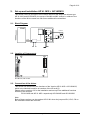
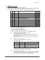
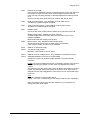
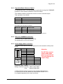
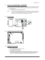
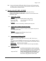
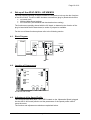
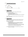
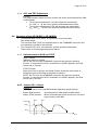
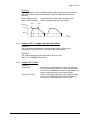
ARSAPE Constant Voltage Step Motor DRIVER USER MAMUAL AD VL M1S + AD VM M1S AD VL M2S + AD VM M2S AD VL M3S + AD VM M3S ©ARSAPE 2005 - Document V4900UM241105_VD-R3.doc Page 2 of 16 User Manual ARSAPE Step Motor DRIVER AD VL M_S + AD VM M_S Contents 1. General Information .......................................................................................................... 3 1.1. 1.2. 1.3. 1.4. Product Description.................................................................................................................... 3 Technical Specifications............................................................................................................. 4 Suitable ARSAPE Motors........................................................................................................... 4 Dimensions and mounting.......................................................................................................... 5 2. Set-up and installation AD VL M1S + AD VM M1S ............................................ 6 2.1. 2.2. 2.3. 2.4. 2.4.1. 2.4.2. 2.4.3. Block Diagram ............................................................................................................................ 6 Location of Components ............................................................................................................ 6 Connection of the drives ............................................................................................................ 6 COMMAND" connector .............................................................................................................. 7 Operation Mode Selector Switch................................................................................................ 9 LED (near COMMAND connector)............................................................................................. 9 Power Supply, Motor Connector ................................................................................................ 9 3. Set-up of the AD VL M2S + AD VM M2S ............................................................. 10 3.1. 3.2. 3.3. 3.4. 3.4.1. 3.4.2. 3.4.3. 3.4.4. Block Diagram .......................................................................................................................... 10 Location of Components AD xx M2S ....................................................................................... 10 Adjustment of the speed .......................................................................................................... 10 Operation of the AD VL M2S + AD VM M2S............................................................................ 11 Jumper ADJ = Adjust ............................................................................................................... 11 Jumper VCO = Voltage Controlled Oscillator........................................................................... 11 Switches/buttons RUN and STOP ........................................................................................... 11 Jumper CK = Clock .................................................................................................................. 11 4. Set-up of the AD VL M3 + AD VM M3.................................................................... 12 4.1. 4.2. 4.3. 4.3.1. 4.3.2. 4.3.3. 4.3.4. 4.4. 4.4.1. 4.4.2. 4.4.3. 4.4.4. Block Diagram .......................................................................................................................... 12 Location of Components .......................................................................................................... 12 Adjustment of the Speed Profile............................................................................................... 12 Speed Profile Graphic Description ........................................................................................... 13 MIN potentiometer.................................................................................................................... 13 MAX potentiometer .................................................................................................................. 13 ACC and DEC Adjustment ....................................................................................................... 14 Operation of the AD VM M3S + AD VM M3S .......................................................................... 14 Switches/buttons RUN and STOP ........................................................................................... 14 Jumper ADJ = Adjust ............................................................................................................... 14 Jumper VCO = Voltage Controlled Oscillator........................................................................... 15 Jumper CK = Clock .................................................................................................................. 15 ©ARSAPE 2005 - Document V4900UM241105_VD-R3.doc Page 3 of 16 1. General Information 1.1. Product Description The drivers AM VL M_S and AD VM M_S are specifically designed for ARSAPE stepper motors ADM0620, AM0820, AM1020, AM1524 and other upcoming ARSAPE step- motors. They offer • Full or half-step • Full-step in ONE and TWO Phase-ON operation for evaluation of motors in low power consumption applications • Voltage Control operation • INHIBIT – not phase current to save energy The main interest of the driver is the fact that the supply voltage can be much higher than with a voltage control driver type. This results in a more constant torque output of the motor up to higher speeds and the possibility to boost motor currents if suitable. These Voltage Mode drivers are available in three different versions .1 AD VL M1 and AD VM M1S Standard stock item Basic drive, composed of a translator (full-step, half-step) and the power drivers, it requires only clock and direction signals and is destined to be controlled by a PC or other host processor. Please refer also to the Product Block Diagram Chapter 2.1 .2 AD VL M2S and AD VM M2S Non-Standard – only available on request Basic drive AD xx M1S and an additional pulse generator to generate on-board a variable clock frequency (on a separate board). Only suitable to be used for tests within the pull-in frequency. Please refer also to the Product Block Diagram Chapter 3.1 .3 AD VL M3 and AD VM M3S Standard stock item Basic drive AD xx M1S with an additional pulse generator and a ramp generator to control acceleration and deceleration of trapezoidal speed profiles to start and stop the motor. This is a standalone step motor controller mainly used for step motor bench tests. Unplugging the blue jumpers will transform the unit into the AD xx M1S. Please refer also to the Product Block Diagram Chapter 4.1 ©ARSAPE 2005 - Document V4900UM241105_VD-R3.doc Page 4 of 16 1.2. Technical Specifications Voltage Mode Drivers, the current established in the motor windings depends only on the applied voltage, the winding resistance and the back-EMF, no current limitation is available. The stepper motor drivers AD xx M_S designed to drive the small stepper motors type with windings calculated for constant voltage drives in AM in full step, wave and half step mode. Power supply voltage Min Max Power supply current AD VL M_S AD VM M_S V 3 14 6 24 mA 16 16 Motor Output current max. mA 400 500 Auxiliary on-board supply Voltage Current V mA 5 50 5 50 Logic input level Conventional Info. Low high V 0 to 0.6 1.6 to 24 0 to 0.6 1.6 to 24 Direction of rotation cw/ccw cw/ccw Step mode full step (two phase ON full-step (one phase ON (wave) half step Step frequency Min max. Dimensions AD VL M1S AD VM M1S AD VL M2S AD VM M2S AD VL M3S AD VM M3S full step/s ----- 0 2000 0 2000 mm 76.3x52x12 76.3x52x22 76.3x52x22 1.3. Suitable ARSAPE Motors Motor Type Driver ADM0620-V3 ADM0620-V6 AM0820-V-3-18AM0820-V-5-56 AM1020-V-3-16AM1020-V-6-65AM1020-V-12-250 AM1524-V-6-35AM1524-V-12-150 AM1524-V-24-590 AD VL M_S AD VM M_S The current level that is established during operation is function of the supplied voltage, the motor and the motor speed. It may be suitable for an application to use a higher voltage to boost torque. This can only be done in combination with the inhibit function which is activated after the ©ARSAPE 2005 - Document V4900UM241105_VD-R3.doc Page 5 of 16 movement to cut the current in the phases to reduce the heat of the motor. Method only suitable for short motion cycles Note: 1. The motor develops a back-EMF which decreases the available voltage to drive current through the coils. 2. At higher speeds, the phase inductance may prevent that the full current is established, the current profile becomes triangular, The consequence of these physical properties is that the torque decreases rapidly with the speed of operation. 1.4. Dimensions and mounting 4x M2x5.3 The drivers are prepared to be mounted using the shown prepared holes on the M1. The M2 and M3 consist of two boards, their assembly is possible by the tapped holes at the bottom of the assembly. 14.2 53.5 48.0 4x∅ 2.70 52.0 76.0 ©ARSAPE 2005 - Document V4900UM241105_VD-R3.doc 12.0 22 AD VM M1S AD VM M2S+3S AD VL M1S AD VL M2S +3S Page 6 of 16 2. Set-up and installation AD VL M1S + AD VM M1S This section refers in principal to all functions offered of the step motor drivers type AD VL M1S and AD VM M1S, the set-up of the M2 and M3 version is, relative to the functions of the M1 the same but offer some additional functionalities. 2.1. Block Diagram Host Translator Phase A M Phase B Clock Direction INH STY GND V+ GND 1 MOTOR OPO F/H DIR 4 Busy 2.2. Location of Components AD VM M1S, AD VL M1S 2.3. Connection of the drives This section will introduce to the functions of the Version AD VL M1S + AD VM M1S, which is the identical board for all versions of the AD ss M_S. Please refer to sections 2.2 for the installation and set-up of the additional functions offered by the versions AD VL M2S and AD VL M3S. respectively AD VM M2S and AD VM M3S Note. Both of these versions can be used as AD VL M1 when the jumpers ADJ, VCO, CK on the mezzanine board are removed. ©ARSAPE 2005 - Document V4900UM241105_VD-R3.doc Page 7 of 16 2.4. COMMAND" connector Input voltage for all inputs variable from 5-24VDC This connector is available on all driver versions, it provides access to all functionality of the respective using through a 12pin header for a processor, PC or PLC. # I/O Type Sign 1 I 1-PH ON 2 I FS/HS 3 I CCW/CW 4 I CLK 5 I RUN 6 I STOP 7 I INHIBIT 8 O BUSY M1 M2 M3 Explanation Full-step; 1-phase ON (wave) X X X Full Step-Half Step mode switch X X X Sense of rotation switch, default = CW X X X External clock input X X X Starts the clock generator ** X X "STOP" : stops the clock generator X X X X X X X X X Disables the phase current(s) Output = Low when clock is active 9 I STY Standby X 10 N VCC +5V power supply, X X X 11 N GND Ground potential ⇒ 0 Volt X X X 12a I VCO External control voltage for the oscillator (VCO) X X O HOME Triggered when Phase 1 is activated with pos current X CLK input is active on positive trigger signal O = Output, for more information please refer to …. I = Input, for more information please refer to … N = Neutral, sink and source pins, to connect directly Functional description of the Inputs/Outputs on COMMAND connector: PIN1, Imposes ONE-Phase ON commutation of the motor, Input is not active if not connected The provided motor torque is equal to the 2-phase-ON control mode, to achieve this, the AD CM M1 increases the current in the activated motor phase by a factor of 1.42, The reached positions are stable, motor will not move if current is switched off PIN2 Imposes full or half step operation, If PIN1 is active, only full-step operation is possible Truth-table for PINS 1 + 2 PIN 1 PIN 2 Function mode Nc Nc Full-step, two phases ON 1.6-24V Nc Full-step, one-phase ON NC 1.6-24V Half-step 1.6-24V 1.6-24V Full-step, one-phase ON The motor torque will be the two phase ON torque at all rotor positions (corrected torque ripple). The driver corrects the current by a factor of 1.41 for all positions of the commutation sequence where one phase is activates. PIN3 Imposes the sense of rotation The signal can be changed at any time, it takes effect after the next following clock signal, it is even possible to trigger a clock and direction at the same time, the step execution is already in the opposite direction. ©ARSAPE 2005 - Document V4900UM241105_VD-R3.doc Page 8 of 16 PIN4 External clock signal, Using this clock enables the host to control the position of the rotor exactly to the number of steps requested. Each positive trigger impulse make the motor move by one step (full-step or half-step dependent on setting of PIN1 or 2). Is has no function when ON-board CLK (versions M2, M3) is active. PIN5 RUN Command trigger - Only available on M2 and M3 version, Activated by a positive edge of the signal PIN6 STOP Command trigger - Only available on M2 and M3 version, Activated by a positive edge of the signal PIN7 INHIBIT signal Current to the motor phases remains ZERO as long as this input is ON. BRAKE signal (ONLY available on AD VL Version) A solder bridge close to this input switches the function of Pin 7 from INHIBIT to BRAKE. Brake means that the windings are shorted. PIN8 BUSY Output - Only available on M2 and M3 version, Active only when internal clock of these drivers are operating Open collector output, not short circuit protected. PIN 9 GND for on-board 5V supply PIN10 +5V power supply output Maximum current 200mA, source output PIN11 GND for the VCO voltage source - Only available on M2 and M3 version PIN12 Selectable between Input VCO or Output HOME the selection is done by a solder bridge behind the command header Functions HOME is a function needed to know the commutation position of the driver. It is activated every time Phase A of the motor is energized with Positive current. This helps to home the clock of the host to the driver commutation a function helpful to avoid step losses when power to the driver is lost. If the motor is stopped with this output triggered the motor will not move uncontrolled upon power-up. VCO Input only available on M2 and M3 version Range = 0 to 2.5V corresponding to Zero Speed 1600Hz (full or half-steps) Note: switching the from full to half step operation or vice versa will not change the motor shaft speed. ©ARSAPE 2005 - Document V4900UM241105_VD-R3.doc Page 9 of 16 2.4.1. Operation Mode Selector Switch To operate the driver, it is also possible to work without using the COMMAND connector, In this case the selection of the Drive Mode The hardware switches replace the need to use the Command Inputs. Their operation is as follows: Switch Switch Function OPO 1-PH ON selector F/H Full-step, Half-step selector DIR Sense of rotation Truth table for the OPO and F/H Switches Status OPO Status F/H OFF OFF Function mode ON OFF/ON Full-step, one-phase ON OFF/ON ON Half-step, two-phase ON* Full-step, two-phase ON * current correction activated, torque remains the same in all rotor positions. 2.4.2. LED (near COMMAND connector) LED active only on when motor is moving not operational on AD VL M1 boards 2.4.3. Power Supply, Motor Connector 1 MOTOR 4 GND V+ The driver comes with a screw type terminal for the connection of the power supply Pin # 1 2 3 4 5 6 Function Phase A + Phase A Phase B +Phase B -+ GND V+ Pin # 1 2 3 4 Motor Phase Phase A + Phase A Phase B + Phase B - Attention Motor PIN 1 2 3 4 Do NOT disconnect motor leads when driver is operational. This will damage the output stage Connector Type: Molex Mating Connector: Housing - Molex 51021-0400 Pins Moles 50058-8000 A cable with this mating connector is not supplied with the driver It is optional and can be ordered with Part Number 2.8000.15.077. It is supplied separately from motor and driver. ©ARSAPE 2005 - Document V4900UM241105_VD-R3.doc Page 10 of 16 3. Set-up of the AD VL M2S + AD VM M2S For hook-up and functions of the AD xx M2S it is required to look-up also the functions of the AD xx M1S. The AD xx M2S includes a mezzanine (plug-in) board which offers: • on-board clock • Single speed setting trough potentiometer Note: The driver AD xx M2S does not offer a speed ramp, it is able to operate he motor only at a single speed which has to be reached during the first step, generally at less than 200-600 Hz (depending on load) 3.1. Block Diagram Host Translator Clock Phase A M Phase B ON/OFF Direction GND V+ FMIN GND Busy 3.2. Location of Components AD xx M2S 1 MOTOR 4 OPO F/H DIR A ADJ B A VCO B CK AD VM M2S, AD VL M2S 3.3. Adjustment of the speed To set-up the motor speed • Turn FMIN potentiometer CCW to zero • Set Jumper ADJ to position A • Set Jumper VCO to position A • See whether the motor starts and adjust FMIN potentiometer until the motor starts with the application load. This determines the maximally possible pull-in frequency. It his however possible to set the speed to any lower value. ©ARSAPE 2005 - Document V4900UM241105_VD-R3.doc Page 11 of 16 Note the motor will reach the MIN speed within the first step (pull-in speed range), no ramp is used. If the motor does not execute please consider the use of the AD VM M3 which includes this option. 3.4. Operation of the AD VL M2S + AD VM M2S • • Jumpers VCO and ADJ in Position A, motor starts upon power up The inputs RUN, STOP have no function Jumper VCO in Position A, Jumper ADJ in Position B, motor will react on the inputs RUN, STOP 3.4.1. Jumper ADJ = Adjust Position A The motor rotates on the set MIN operation speed settings. Button/input RUN: Button/Input STOP: motor will operate at FMIN speed motor will stop Position B No function, do not use this setting, undefined speed may occur. 3.4.2. Jumper VCO = Voltage Controlled Oscillator Position A The on-board frequency generator is activate, motor speed is set by the onboard FMIN potentiometer. Position B The external Analogue Speed Reference input is used (PIN 12 on COMMAND connector), 3.4.3. Switches/buttons RUN and STOP (buttons not present on all boards) Condition for correct function JMP. ADJ in Pos. B, JMP. VCO in Pos. A, NOTE: PIN 5 and 6 on the COMMAND connector has the same identical function, in case that the PIN 5 is activated (5 to 24VDC applied), the RUN button has no function. RUN Function: Starts the motor to operate, STOP Function Stops the motor to operate, the motor stops immediately 3.4.4. Jumper CK = Clock Jumper SET, Jumper NOT SET: the internal clock generator is active If an external clock is used at the same time (clock signal present on PIN 4 on COMMAND connector), the speed is no longer controlled by any of the clock signals. Only the external Clock Signal (clock signal present on PIN 4 on COMMAND connector) will be taken into account, ramp generator is OFF as well. ©ARSAPE 2005 - Document V4900UM241105_VD-R3.doc Page 12 of 16 4. Set-up of the AD VL M3S + AD VM M3S For hook-up and functions of the AD xx M3S it is required to look-up also the functions of the AD xx M1S. The AD xx M3S includes a mezzanine (plug-in) board which offers: • on-board clock • MIN and Max Speed settings • ACC and DEC (acceleration and deceleration time setting) The functions are partially shared with the M1 board, to determine the function of the plug-in board with the M1 base board, a series of jumpers is available. For the use of these functions please refer to the following section 4.1. Block Diagram Host Translator Clock Phase A Profile M Phase B ON/OFF Direction GND V+ FMIN FMAX GND Acc Dec 1 MOTOR OPO F/H DIR 4 Busy 4.2. Location of Components STOP RUN A ADJ B A VCO B CK AD VM M3S, AD VL M3S 4.3. Adjustment of the Speed Profile The Potentiometers MIN, MAX, ACC, DEC located on the Mezzanine Board (plugged into the AD VL M1 board) allow to set the parameters of the Speed profile used to move the motor. The function and adjustment methods are explained below. ©ARSAPE 2005 - Document V4900UM241105_VD-R3.doc Page 13 of 16 4.3.1. Speed Profile Graphic Description MAX MIN tacc tdec Time 4.3.2. MIN potentiometer Function: The potentiometer serves to set the minimum speed of the motor. To set-up the minimum speed • Turn MAX potentiometer CCW to zero • Set Jumper ADJ to position B • Press Start to see whether the motor starts and adjust MIN potentiometer until the motor starts with the application load. Note, the motor will reach the MIN speed within the first step (pull-in speed range), no ramp is used 4.3.3. MAX potentiometer Function: The potentiometer is used to determine the maximum speed the motor will reach. To reach this speed the motor will require and acceleration and a deceleration ramp respectively. The set-up is done as follows: • SET_UP MIN speed • Increase the ACC and DEC ramp by adjusting the corresponding potentiometers on the board (see ACC and DEC Adjustment) • Increase the MAX speed by turning CW • If the motor does not accelerate to the speed (stalling of motor shaft) increase the ACC time (acceleration time given to the motor to reach the MAX speed) by turning the ACC potentiometer CCW NOTE: Maximum speed changes as well when MIN setting is changed, the difference is not changing ©ARSAPE 2005 - Document V4900UM241105_VD-R3.doc Page 14 of 16 4.3.4. ACC and DEC Adjustment Function: The potentiometers adjust the time at which the motor will accelerate from MIN to MAX speed. Turning the potentiometer CW will increase the acceleration (tacc and tacc Ì), the motor speed increases/decreases faster Turning the potentiometer CCW will decrease the acceleration ((tacc and tacc Ê), the motor speed increases/decreases slower 4.4. Operation of the AD VM M3S + AD VM M3S • • The Buttons RUN, STOP allow, to operate the motors manually. See details below. The functions RUN, STOP are available also on the COMMAND connector and are operating in parallel to the switches. The Jumpers ADJ, VCO, CK determine specific operation parameters. Please refer to the corresponding section below. 4.4.1. Switches/buttons RUN and STOP RUN Function: Starts the motor to operate, NOTE: the PIN 5 on the COMMAND connector has the same identical function, in case that the PIN 5 is activated (5 to 24VDC applied), the RUN button has no function STOP Function Stops the motor to operate, the actual function is that the motor starts to decelerate the moment Stop is activated or pressed, NOTE: the PIN 5 on the COMMAND connector has the same identical function, in case that the PIN 5 is activated (5 to 24VDC applied), the RUN button has no function 4.4.2. Jumper ADJ = Adjust Position A The motor rotates on the set MIN and Max operation speed settings. Button RUN pressed: Button STOP pressed: Speed Start Acceleration from MIN speed to MAX speed Motor will decelerate but will continue to run at the speed setting of the MIN. Stop MAX MIN tacc tdec ©ARSAPE 2005 - Document V4900UM241105_VD-R3.doc Time Page 15 of 16 Position B The motor rotates on the set MIN and Max operation speed settings but will stop automatically after the deceleration (when the MIN speed has been reached) Button RUN pressed: Button STOP pressed: Speed Start Acceleration from MIN speed to MAX speed Motor will decelerate and stop rotating Stop MAX MIN tacc tdec Time 4.4.3. Jumper VCO = Voltage Controlled Oscillator Position A The on-board ramp generator is activated and used to influence the acceleration time of the motor from Min to Max clock speed. Position B The external Analogue Speed Reference input is used (PIN 12 on COMMAND connector) 4.4.4. Jumper CK = Clock Function: Jumper SET, Jumper NOT SET: the internal clock generator is active If an external clock is used at the same time (clock signal present on PIN 4 on COMMAND connector), the speed is no longer controlled by any of the clock signals. Only the external Clock Signal (clock signal present on PIN 4 on COMMAND connector) will be taken into account, ramp generator is OFF as well. ©ARSAPE 2005 - Document V4900UM241105_VD-R3.doc Page 16 of 16 RevisionsV4900UM230904_VD-R0 Initial release V4900UM180105_VC-R1 New feature on VL Brake input V4900UM280805_VD_R2 Safety Warning V4900UM241105_VD_R3 Correction of cable indication 23.9.04 24.11.05 Product denominator key Typical Product type AD VM M1S AD ARSAPE Driver V V = Constant Voltage drive M L M = LOW supply voltage 3-14V = MEDIUM supply voltage 6-24V M1 Function Mode M1 = Pulse + direction drive, external control M2 = Speed control drive w/o speed ramp M3 = Speed control drive with speed ramp S External connection type S = screw type for all connectors SP = Screw type for supply and motor, pins for COMMAND (Special pin out) ©ARSAPE 2005 - Document V4900UM241105_VD-R3.doc