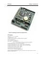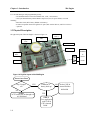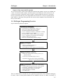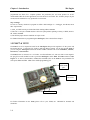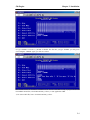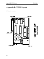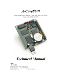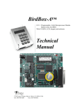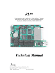
1
586-Engine™ C/C++ Programmable, 100/133 MHz 32-bit Controller with Floating Point Unit, 19 ADCs, and 8 DACs Technical Manual 1724 Picasso Avenue, Suite A, Davis, CA 95616-0547, USA Tel: 530-758-0180 Fax: 530-758-0181 Internet Email: [email protected] http://www.tern.com COPYRIGHT 586-Engine, A-Engine86, A-Engine, A-Core86, A-Core, i386-Engine, V25-Engine, MemCard-A, MotionC, MotionC2140, P100, VE232, NT-Kit, and ACTF are trademarks of TERN, Inc. Am188ES and Am186ES are trademarks of Advanced Micro Devices, Inc. Borland C/C++ is a trademark of Borland International. MS-DOS, Windows, Windows95/98/2000 are trademarks of Microsoft Corporation. IBM is a trademark of International Business Machines Corporation. Version 1.1 June 19, 2001 No part of this document may be copied or reproduced in any form or by any means without the prior written consent of TERN, Inc. © 1993-2000 1724 Picasso Avenue, Suite A, Davis, CA 95616-0547, USA Tel: 530-758-0180 Fax: 530-758-0181 Internet Email: [email protected] http://www.tern.com Important Notice TERN is developing complex, high technology integration systems. These systems are integrated with software and hardware that are not 100% defect free. TERN products are not designed, intended, authorized, or warranted to be suitable for use in life-support applications, devices, or systems, or in other critical applications. TERN and the Buyer agree that TERN will not be liable for incidental or consequential damages arising from the use of TERN products. It is the Buyer's responsibility to protect life and property against incidental failure. TERN reserves the right to make changes and improvements to its products without providing notice. 586-Engine Table of Contents Table of Contents Chapter page 1. Introduction ................................................. 1-1 1.1 Functional Description .......................... 1-1 1.2 Features ................................................ 1-3 1.3 Physical Description .............................. 1-4 1.4 586-Engine Programming Overview ...... 1-5 1.5 P100 & VE232 ..................................... 1-6 1.6 Minimum Requirements ........................ 1-6 1.6.1 Minimum Hardware Requirements 1-7 1.6.2 Minimum Software Requirements.. 1-7 2. Installation ................................................... 2-1 2.1 Software Installation ............................. 2-1 2.2 Hardware Installation ............................ 2-1 2.2.1 Connecting the VE232 to the 586-Engine .................................... 2-1 2.2.2 Connecting the 586-Engine to the PC ............................................ 2-2 2.2.3 Powering-on the 586-Engine.......... 2-3 3. Hardware ..................................................... 3-1 3.1 SC520 – Introduction ........................... 3-1 3.2 SC520 – Features ................................. 3-1 3.2.1 Clock ............................................ 3-1 3.2.2 Programmmable interrupt control and external interrups ........................... 3-1 3.2.3 Asynchronous Serial Ports ............ 3-2 3.2.4 GP timers ...................................... 3-2 3.2.5 PIT timers ..................................... 3-3 3.2.6 Software timers ............................. 3-3 3.2.7 SSI ................................................ 3-3 3.2.8 RTC .............................................. 3-3 3.2.9 Watchdog timer ............................ 3-3 3.2.10 PCI, DMA, SDRAM, W/R buffer. 3-3 3.2.11 SC520 PIOs ................................ 3-3 3.3 I/O Mapped devices .............................. 3-5 3.3.1 I/O Space ...................................... 3-5 3.3.2 P2543, 12-bit serial ADC ............... 3-6 3.3.3 Dual 12-bit DAC............................ 3-7 3.3.4 AD7852, Parallel 12-bit ADC ........ 3-7 3.3.5 DA7625, Parallel 12-bit DAC ........ 3-8 3.3.6 UART SCC2691 ........................... 3-8 3.4 Power Supplies and Supervisor ............. 3-8 3.5 Headers and Connectors......................... 3-9 Chapter page 3.5.1 Expansion Headers J1 and J2 ........ 3-9 3.5.2 J4 Connector for ADC, DAC ........3-11 3.5.3 Interrface to P100 and MotionC....3-11 4. Software ...................................................... 4-1 4.1 Programming overview ......................... 4-2 4.1.1 Steps for 586-based product development .................................. 4-3 4.2 586.LIB ................................................ 4-5 4.3 Functions in 586.OBJ ........................... 4-5 4.3.1 586-Engine Initialization .............. 4-5 4.3.2 External Interrupt Initialization .... 4-6 4.3.3 I/O Initialization ........................... 4-7 4.3.4 Timer Units .................................. 4-8 4.3.5 Analog-to-Digital Conversion ....... 4-9 4.3.6 Digital-to-Analog Conversion ......4-10 4.3.7 Other Library Functions ..............4-10 4.4 Functions in SER0.OBJ/SER1.OBJ ......4-12 4.5 Functions in SCC.OBJ .........................4-17 Appendices: A. 586-Engine Layout................................A-1 B. VE232 Pin Layout................................. B-1 C. UART SCC2691 ..................................C-1 D. CMOS RAM Map ................................D-1 Schematics: 586-Engine i 586-Engine Chapter 1: Introduction Chapter 1: Introduction 1.1 Functional Description Measuring 3.6 x 2.3 x 0.3 inches, the 586-Engine(5E) is a C/C++ programmable microprocessor module based on a 100/133 MHz, 32-bit CPU (ElanSC520, AMD). Features such as its low cost, compact size, surface-mount flash, high performance floating point coprocessor, and reliability make the 5E ideal for industrial process control and applications requiring intensive mathmatical computation. It is designed for embedded applications that require compactness and high reliability. The 586-Engine (5E) integrates an Am586 CPU and high performance ANSI/IEEE 754 compliant hardware floating point unit (FPU). It provides arithmetic intructions to handle various numeric data types and formats and transcendental functions for sine, cosine, tangent, logarithms, etc, useful for intensive computational applications. Special Note: The core of the Am520 CPU operates at +2.5V and the I/O operation at +3.3V. Also, the input for the I/O is +5V compatable. Stresses above these can cause permanent damage to the SC520 CPU. Operation above these values is not recommended, and can effect device reliability. SRAM 586-Engine SCC2691 UART U8 512 KB 16-bit U9 Am5x86 FLASH J9 watchdog enable 691 CPU 512 KB 16-bit U1 100/133MHz D4..D15 11 ch. 12-bit ADC P2543 U14 2 ch. 12-bit DAC 2 ch. 12-bit DAC LT1446 LT1446 U05 U5 FPU 16-Bit Timers(7) Ext. Interrupts(15) 32 I/O lines RTC/CMOS RAM ROM/Flash Cont. (2) 16550 UARTs SSI Watchdog Timer Interupt Controller D4..D15 8 ch. 12-bit ADC AD7852 U12 4 ch. 12-bit DAC DA7625 U11 REF U13 J5 J4 J1 & J2 Figure 1.1 Functional block diagram of the 586-Engine The 586-Engine boots up from on-board 512KB ACTF Flash, and supports up to 512KB battery-backed SRAM. No SDRAM, PCI, or DMA supported. The on-board Flash has a protected boot loader and can be 1-1 Chapter 1: Introduction 586-Engine easily programmed in the field via serial link. Users can download a kernel into the Flash for remote debugging. With the DV-P and ACTF Flash Kit support, user application codes can be easily fieldprogrammed into and run out of the Flash. A real-time clock* (RTC72423) provides information on the year, month, date, hour, minute, and second, in addition to a 100-year calender and 114 bytes of general purpose battery-backed RAM. This RAM is used by the real-time clock, as well as the ACTF to store the jump address as the pointer to the users application code. Two industy-standard UARTs support high-speed, reliable serial communication at a rate of up to 1.152 M baud via RS-232 drivers. One synchronous serial interface (SSI) supports full-duplex bi-directional communication. An optional UART SCC2691 may be added in order to have a third UART on-board. All three serial ports support 8-bit and 9-bit communication. There is one programmable interval timer (PIT) providing 3 16-bit PIT timers and 3 16-bit GP timers, and a software timer. The timers support timing or counting external events. The software timer provides a very efficient hardware timebase with microsecond resolution. In addition, there are two supervisor chips that monitor for power failure, watchdog and system reset. The 586-Engine provides 32 user-programmable, multifunctional I/O pins from the CPU. Most of the PIO lines share pins with other functions. The 586E supports up to 15 external interrupts. No repair support is available for the 388 pin BGA SC520. A high-speed, up to 300K samples per second, 8-channel, 12-bit parallel ADC* (AD7852) can be installed. This ADC includes sample-and-hold and precision internal reference, and has an input range of 0-5 V. The 586-Engine also supports a 4-channel, high-speed parallel DAC* (DA7625, 0-2.5V). An optional 12-bit serial ADC (P2543) has 11 channels of analog inputs with sample-and-hold and a 5V reference that facilitate ratiometric conversion, scaling, and isolation of analog circuitry from logic and supply noise, supporting conversion up to a sample rate of approximately 10 KHz. Up to two optional 2channel, 12-bit serial DAC (LT1446) that provides 0-4.095V analog voltage outputs capable of sinking or sourcing 5mA are also available. Overall the 5E can support up to 8 analog outputs and 19 analog inputs. An optional P100 I/O expansion board can provide regulated 5V power and RS-232/RS-485 drivers for the 5E. Figure 1.2 The P100 I/O expansion board The 586-Engine can be installed on TERN controllers such as the P300, PowerDrive, PC-Co, LittleDrive, or MotionC (see Figure 1.3). TERN also offers custom hardware and software design, based on the 586-Engine or other TERN controllers. 1-2 586-Engine Chapter 1: Introduction Figure 1.3 A 586-Engine installed on the MotionC2140 1.2 Features • Dimensions: 3.6 x 2.3 x 0.3 inches • Temperature:-40°C to +80°C • 133MHz, 32-bit CPU (ElanSC520, AMD), Intel 80x86 compatible • Easy to program in C/C++ • Power consumption: 440 mA at 5V • Power input: +5V regulated DC, or + 9V to +12V unregulated DC with P100 expansion board installed* • 512 KB SRAM, 512 KB, 114 byte internal CMOS RAM • 8-channel 300 KHz parallel 12-bit ADC (AD7852) with 0-5V analog input* • 4-channel 200 KHz parallel 12-bit DAC (DA7625) with 0-2.5V analog output* • 2 channels serial 12-bit DAC (LT1446), 10 KHz * • 11 channels serial 12-bit ADC (P2543), 10 KHz * • High performance floating point coprocessor • Up to 1GB memory expansion via MemCard-A • Up to 3 serial ports (2 from ElanSC520, plus one optional SCC2691 UART) support 8-bit or 9-bit asynchronous communication * 1-3 Chapter 1: Introduction 586-Engine • 15 external interrupts with programmable priority • 32 multifunctional I/O lines from ElanSC520, 1 SSI, 7 16-bit timers • 114 bytes internal battery-backed RAM. Supervisor (691) for power failure, reset and watchdog • Real-time clock (RTC72423), lithium coin battery* • P100 I/O expansion board for regulated 5V power, RS-232/485 drivers, and TTL I/O lines* * optional 1.3 Physical Description The physical layout of the 586-Engine is shown in Figure 1.4. 11 ch. Serial ADC 8 ch. parallel ADC 2 ch. serial DAC’s 512K SRAM 512K Flash 4 ch. parallel DAC J2 Pin 38 Pin 40 3rd UART Figure 1.4 Physical layout of the 586-Engine Power On or Reset Step 2 jumper set? YES Validation of battery back up? NO STEP 1 ACTF menu sent out through ser0 at 19200 baud 1-4 STEP 2 JUMPER YES STEP 2 Go to application code CS:IP in CPU's internal RAM NO Set the CS:IP in internal RAM to 8000:0000 586-Engine Chapter 1: Introduction Figure 1.5 Flow chart for ACTF operation The “ACTF boot loader” resides in the 512KB on-board Flash chip (29F400). At power-on or RESET, the “ACTF” will check the STEP 2 jumper. If STEP 2 jumper is not installed, the ACTF menu will be sent out from serial port0 at 19200 baud. If STEP 2 jumper is installed, the5E will check for a valid battery back-up. If present the 5E will go to the jump address stored in the CPU’s 114 bytes of general purpose RAM. Without a valid battery back up, the 5E will write the address 0x80000 to the inernal RAM, and then go to that address. 1.4 586-Engine Programming Overview Steps for 5E-based product development: Preparation for Debugging • Connect 5E to PC via RS-232 link, 19,200, 8, N, 1 • Power on 5E without STEP 2 jumper installed • ACTF menu should be sent to PC terminal • Use “D” command to download “L_29f400.HEX” in SRAM • Use “G” command to run “L_29f400” • Download “5860_115.HEX” to Flash starting at 0x80000 • Use “G” command to set jump address and run debugger • Install the STEP2 jumper (J2.38-40) • Power-on or reset 5E, Ready for Remote debugger STEP 1: Debugging • Write your application program in C • Build project in Paradigm C++ • Edit, compile, link, locate, download, and remote-debug STEP 2: Standalone Field Test 8Setup Jump Address(default 0x08000), points to your program in SRAM 8Power off, install STEP2 jumper, Power on 8application program running in battery-backed SRAM (Battery lasts 3-5 years under normal conditions.) STEP 3: Production (DV-P+ACTF Kit only) • Generate application HEX file with DV-P and ACTF Kit • Download “L_29F400.HEX” into RAM and Run it • Download application HEX file into FLASH • Modify jump address to 0x80000 • Set STEP2 jumper There is no ROM socket on the 5E. The user’s application program must reside in SRAM for debugging in STEP1, reside in battery-backed SRAM for the standalone field test in STEP2, and finally be 1-5 Chapter 1: Introduction 586-Engine programmed into Flash for a complete product. For production, the user must produce an ACTFdownloadable HEX file for the application, based on the DV-P+ACTF Kit. The “STEP2” jumper (J2 pins 38-40) must be installed for every production-version board. Step 1 settings In order to correctly download a program in STEP1 with Paradigm C++ Debugger, the 5E must meet these requirements: 1) 5860_115.HEX must be pre-loaded into Flash starting address 0x80000. 2) The CPU’s 114 bytes of RAM must have the correct jump address pointing at 5860_115.HEX, which is the address 0x80000. 4) The STEP2 jumper must be installed on J2 pins 38-40. For further information on programming the 586-Engine, refer to the Software chapter. 1.5 P100™ & VE232 The P100 ™ is an I/O expansion board for the 586-Engine that provides regulated +5V DC power and RS-232/485 drivers. It converts TTL signals to and from RS-232 signals. You do not need the P100 if you are using the 586-Engine installed on another TERN controller such as the LittleDrive, MotionC, PowerDrive, or SensorWatch. The P100, shown in, measures 4.4 x 2.5 inches. A wall transformer (9V, 300 mA) with a center negative DC plug (Ø=2.0 mm) should be used to power the 586-Engine via the P100. The P100 connects to 586Engine via J1 and J2 (2x20 headers). SER0 (H2) and SER1 (H3) on the P100 are 2x5-pin headers for serial ports SER0 and SER1. SER0 is the default programming port. Ser0 Default debub port 9-35V DC Power 48 TLL I/Os For further information on the P100, please refer to your TERN, Inc. CD-ROM for manauls and schematics. 1-6 586-Engine Chapter 1: Introduction In addition to the P100 I/O expansion controller, the optional VE232 interface board can also supply regulated +5V and RS-232/RS-485 drivers. Although the VE232 comes standard with a linear power regualtor, because of the power comsumption of the 586-Engine (440mV @ 5V) a switching regulator is mandatory on the VE232 interface card. The VE232 installs on the 586-Engine via a 2x10 pin header on the J2 header of the 586-Engine. The VE232 measures 1.57”x2.30”. A picture is shown. 1.6 Minimum Requirements for 586-Engine System Development 1.6.1 Minimum Hardware Requirements • • • • • PC or PC-compatible computer with serial COMx port that supports 115,200 baud 586-Engine controller P100 I/O expansion board* PC-V25 serial cable (RS-232; DB9 connector for PC COM port and IDE 2x5 connector for controller) center negative wall transformer (+9V, 500 mA) * NOTE: the P100 is not needed if you are using the 5E installed on another controller 1.6.2 Minimum Software Requirements • TERN EV-P installation CD-ROM and a PC running: Windows 3.1/95/98/2000 With the EV-P, you can program and debug the 586-Engine in Step One and Step Two, but you cannot run Step Three. In order to generate an application Flash file and complete a project, you will need both the Development Kit (DV-P Kit) and the ACTF Flash Kit. 1-7 586-Engine Chapter 2: Installation Chapter 2: Installation 2.1 Software Installation Refer to the Technical manual “EV-P&DV-P Kit” on TERN CD under tern_docs\manual. By manufacture default, 586-Engines are ready for Paradigm C++ debug with STEP2 jumper installed, CMOS RAM setup for 0x80000, and 5860_115 debug kernel resides in Flash starting 0x80000. Power on, the on-board LED should blink twice indicating running debug kernel. You DO NOT have to download debug kernel into flash again. You can SKIP the operation discussed in 2.2 below. 2.2 Prepare 586-Engine for Paradigm C++ TERN Edition 1) Start Paradigm C++. Select from Top menu: Tool, RTLOAD, A HEX file Loader window will be shown. 2-1 586-Engine Chapter 2: Installation 2) F5=Select Baud, to setup 19200. 3) F8=Select .HEX file from c:\tern\586\rom\L_29F400.HEX 3) Power on the 586-Engine with the STEP2 jumper off, the ACTF menu will show up. 2-2 586-Engine Chapter 2: Installation 4) Caps Lock on your PC keyboard, Type “D” command, then enter. 5) F6 = Upload .HEX file, from PC to 586 SRAM. 2-3 586-Engine Chapter 2: Installation 6) Type “G04000” to run the “L_29F400” in SRAM. The first time you type “G04000” you will get an error. Doing the “G04000” again, you will see as below The 29F400 Flash sector 0x80000 to 0xFBFFF will be erased. It will then be ready to program Flash with new DEBUG kernel file (c:\tern\586\rom\5860_115.hex), or user application .HEX. 7) F8= Select .HEX file, from c:\tern\586\rom\5860_115.hex. 2-4 586-Engine Chapter 2: Installation 8) F6=Upload .HEX file to program the 5860_115 debug kernel into Flash starting address 0x80000. After programming the Flash, 586-Engine will automatically reset. “G80000” to setup the EE Jump Address, and start the DEBUG kernel. The on-board LED should blink twice and then stay on, indicating 586-Engine is ready for remote DEBUGING. Power off the controller. Install the STEP2 Jumper, then power on, the LED blink twice. Use F9 = Exit. The 586-Engine is ready for using Paradigm C++ TERN Edition to download, debug, and run. There are two sample projects in the c:\tern\586 directory (default working directory): 2-5 586-Engine Chapter 2: Installation led.ide and test.ide. Go to “File” and open the sample project file, then build and download. There are many sample programs under c:\tern\586\samples. After you debug your application code, you can setup the 586-Engine to run in Standalone Mode. Standalone Mode(STEP2): By default, the Paradigm C++ TERN Edition will download your application code starting at 0x08000 in the battery backed SRAM. Power off 586-Engine. Remove STEP2 jumper. On PC side, click TOOL, RTLOAD. Power on 586-Engine again without STEP2 jumper, then the ACTF menu should show up. At the ACTF menu prompt, type “G08000” to setup the Jump Address and run your application. Power off, Install the STEP2 Jumper. Then at power on, controller will jump to 0x08000 in SRAM and run your application. 2.3 Hardware Installation Overview • Install VE232 (Requires switching regulator): H1 connector of VE232 installs on J2 of the 586-Engine • Connect PC-V25 cable: For debugging (STEP 1), place IDE connector on SER0 with red edge of cable at pin 1 • Connect wall transformer: Connect 9V wall transformer to power and plug into power jack Hardware installation for the 586-Engine consists primarily of connecting the microcontroller to your PC. For the 586-Engine, the VE232 must be used to supply regulated power and RS232 drivers, or use the 586-Engine installed on P100 controller, please refer to the technical manual for that controller for installation information. 2.3.1 Connecting the VE232 to the 586-Engine Figure 2.1 Before installing the VE232 on the 586-Engine 2-6 586-Engine Chapter 2: Installation Figure 2.2 After installing the VE232 on the 586-Engine Install the VE232 interface with the H1 (10x2) socket connector on the upper half of the J2 (dual row header) of the 586-Engine. 2.4 Connecting the 586-Engine to the PC The 586-Engine+VE232 can be linked to the PC via a serial cable (PC-V25). Install the 5x2 IDC connector on the SER0 header of the VE232. IMPORTANT: Note that the red side of the cable must point to pin 1 of the VE232 H1 header. The DB9 connector should be connected to one of your PC's COM Ports (COM1 or COM2; by default, the Paradigm software will use COM1) RED side of serial cable corresponding to pin 1 of headers for SER0/SER1 To SER0 for debugging SER1 SER0 To COM1 or COM2 SRAM IDC connector PC Pin 1 of headers for SER0 &SER1 74 HC H1 on VE232 14 1489 U5 EE 1488 U6 485 U1 PP1 ADC 9-pin connector U A R T RTC 7662 J6 U4 J2 power jack EPROM AMD AM188ES CPU 691 VE232 A-Engine Figure 2.3 Connecting the 586-Engine and VE232 to the PC 2-7 586-Engine Chapter 2: Installation 2.4.2 Powering-on the 586-Engine Connect a wall transformer +9V DC output to the VE232 DC power jack, or, for the P100, to the DC power jack. 2.4.3 586-Engine installed on a P100 2-8 586-Engine™ Chapter 3: Hardware Chapter 3: Hardware 3.1 SC520 - Introduction The 586-Engine is based on AMD Elan SC520 Microcontroller. It includes an industry-standard Am5x86 CPU with floating point unit (FPU). It provides a General-Purpose (GP) bus with programmable timing for 8 and 16-bit devices. A ROM/Flash controller supports on-board high performance code execution. An enhanced programmable interrupt controller (PIC) prioritizes 22 interrupt levels with up to 15 external sources. Two Async UARTs can operate up to 1.15 M bit/s. A Sync serial interface (SSI) offers full-duplex or half-duplex operation to support on-board ADC/DACs and user expansion. A real time clock, a software timer, 3 GP timers, and 3 programmable interval timers are all included. 32 programmable I/O pins are onboard. Please refer to the SC520 User’s Manual, SC520 Data Sheet, and SC520 Register Set Manual included on TERN’s CD (TERN’s EV-P/DV-P kit), under AMD_docs sub-directory. 3.2 SC520 – Features 3.2.1 Clock One 32.768 KHz and one 33.333 MHz crystal are installed to provide all the clocks required for CPU, Real time clock, UART, timers, and clock output. The CLKTEST (CLKT) signal is routed to J1 pin 4. Software can select to output one of 6 internal clocks, including 32.768K, 1.8443 MHz, 18.432 MHz, 1.1882 MHz, 1.47456 MHz, and 36.864 MHz. On-board ADC (U12) can use 1.8432 MHz as ADC clock. 3.2.2 Programmable interrupt controller and external Interrupts The Programmable Interrupt Controller (PIC) prioritizes 22 interrupt levels (P1-P22) with up to 15 external sources (GPIRQ0-10 and INTA-D). A programmable router must be programmed to map internal or external interrupt sources to the master or two of slave interrupt controllers to provide different priorities, from P1 to P22. All 15 external interrupt requests are programmed as edge sensitive, after 586_init(); An example map for P1 to P22 is listed below and tested in sample program 586_intx.c. // There are 22 interrupt priority levels plus NMI // There are 15 external interrupt requests (GPIRQ0-10, /INTA-D) // Example internal interrupt map by TERN: // P1=Master PIC IR0, interrupt vector=0x40, PIT timer0 // P2=Master PIC IR1, interrupt vector=0x41, GPIRQ0=PIO23=J2.33 // P3=slave1 PIC IR0, interrupt vector=0x48, RTC // P4=slave1 PIC IR1, interrupt vector=0x49, GPIRQ1=PIO22=J2.23 // P5=slave1 PIC IR2, interrupt vector=0x4a, GPIRQ2=PIO21=J2.21 // P6=slave1 PIC IR3, interrupt vector=0x4b, GPIRQ3=PIO20=J2.19 // P7=slave1 PIC IR4, interrupt vector=0x4c, GPIRQ4=PIO19=J2.20 // P8=slave1 PIC IR5, interrupt vector=0x4d, FPU // P9=slave1 PIC IR6, interrupt vector=0x4e, /INTD=SCC=J3.14 // P10=slave1 PIC IR7, interrupt vector=0x4f, GP timer1/INTC=J3.13 // P11=Master PIC IR3, interrupt vector=0x43, SER2/0 // P12=Master PIC IR4, interrupt vector=0x44, SER1 3-1 Chapter 3: Hardware // // // // // // // // // // P13=Slave2 P14=Slave2 P15=Slave2 P16=Slave2 P17=Slave2 P18=Slave2 P19=Slave2 P20=Slave2 P21=Master P22=Master PIC PIC PIC PIC PIC PIC PIC PIC PIC PIC 586-Engine™ IR0, IR1, IR2, IR3, IR4, IR5, IR6, IR7, IR6, IR7, interrupt interrupt interrupt interrupt interrupt interrupt interrupt interrupt interrupt interrupt vector=0x50, vector=0x51, vector=0x52, vector=0x53, vector=0x54, vector=0x55, vector=0x56, vector=0x57, vector=0x46, vector=0x47, GP timer0 GPIRQ5=PIO18=J2.17 GPIRQ6=PIO17=J2.18 GPIRQ7=PIO16=J2.15 PIT timer1 GPIRQ8=PIO15=J2.16 GPIRQ9=PIO14=J2.6 GPIRQ10=PIO13=J2.8 PIT Timer2/INTB=J3.12 GP timer2/INTA=J3.11 See the sample program in c:\tern\586\samples\5e\586_intx.c for more details. The 586-Engine uses vector interrupt functions to respond to external interrupts. Refer to the SC520 User’s manual for more information about interrupt vectors. 3.2.3 Asynchronous Serial Ports The SC520 has two 16450/16550-compatible asynchronous serial channels: SER0/2 and SER1. Both asynchronous serial ports support the following: • Full-duplex operation, • 5-, 6-, 7-, and 8-bit data transfers • Odd, even, and no parity • 1, 1.5, or 2 stop bits • Error detection • Hardware flow control • Transmit and receive interrupts for each port • Maximum baud rate, up to 1.152 MHz The software drivers for each serial port implement a ring-buffered interrupt transmitting and receiving arrangement. See the samples files s1_echo.c and s0_echo.c. An optional SCC2691 UART can be installed on-board, in U8. 3.2.4 GP Timers Three 16-bit General-Purpose Timers are on-board. Two external inputs, TIN0=J4.4 and TIN1=J6, can be used for the GP Timer0 and Timer1 to capture and count external pulses up to 33.333 MHz/4. Timer 0 and Timer1 can output pulses on TOUT0=J4.3 and TOUT1=J4.5. GP Timers support interrupt on terminal count, continue mode, and square wave generation. Timer2 is not connected to any external pin. It can be used as an internal timer for real-time coding or time-delay applications. It can also prescale timer0 and timer1. See the sample programs timer02.c and tmr_out.c in the tern\586\samples\5e directory. 3.2.5 PIT Timers Three 16-bit Programmable Interval Timers (PIT) are on-board. Each PIT channel has one interrupt output. Only PIT2 has an external output pin and can provide square wave output. All PITs supports interrupt on terminal count, hardware-retriggerable one-shot and timer functions. See samples at c:\tern\586\samples\5e directory for 586_pit0.c and pit2_out.c. 3-2 586-Engine™ Chapter 3: Hardware 3.2.6 Software timers The “software timer” is actually a hardware timer, which is intended to provide a millisecond timebase with microsecond resolution. Ideal applications for this function include providing a system wide timebase, and precise measurement of the time between events. The software timer has a 16-bit microsecond counter that increments with a period of one millisecond. This yields a maximum duration of 65.5 seconds. A microsecond latch register that provides the number of microseconds since the last time that the millisecond register was read. The software timer provides a very efficient hardware timerbase for use by software. It is designed to replace the traditional method of system timebase generation. Traditional system timebase generation is accomplished by programming a timer to generate a periodic interrupt. The interrupt service routine then increments a counter. This value is often kept in a global variable, which can then be accessed by other code that needs to track time. The problem with this traditional timebase is caused by interrupt latency and possible missed interrupt. The software timer included can be used to resolve these problems. See more details on AMD SC520 Users’ Manual, chapter 18. 3.2.7 SSI A synchronous serial interface (SSI) provides full-duplex and half-duplex, bi-directional communication at a software programmable SSI clock speed, from 64K Hz to 8MHz. 586-Engine uses the SSI to interface to the serial ADC(TLC2543) and the serial DAC(LTC1446) with independent chip enable control. User can use the SSI to interface many types of external serial peripheral devices. See the sample c:\tern\586\samples\5e\ssio.c. 3.2.8 RTC A battery backed up real-time clock (RTC) is included. The RTC consists of time-of-day clock with alarm and a 100-year calendar. It has also a programmable periodic interrupt and 114 bytes of static user RAM. See samples 586_rtc.c and rtc_pint.c for more details. 3.2.9 Watchdog timer The Watchdog timer included in SC520 is not disabled. The 586-Engine uses a 691 supervisor chip to monitor the 5V power and provides an external watchdog. User can activate the 691 watchdog with a jumper setting on H1. 3.2.10 PCI, DMA, SDRAM, Write/Read buffer No SDRAM support on the 586-Engine. No support on PCI, DMA, and Write/Read buffer. 3.2.11 SC520 PIOs The SC520 supports 32 user-programmable I/O lines (PIO). Each of these pins can be used as a userprogrammable input or output signal, if the interface function is not needed. The 586-Engine PIO pins are 3.3V output and all inputs are 5V tolerant. Absolutely no voltage greater than 5V should be applied to any pins. Over 5V voltage input can cause permanent damage. 3-3 Chapter 3: Hardware 586-Engine™ After power-on/reset, PIO pins default to various configurations. The initialization routine, sc_init();, provided by TERN libraries reconfigures some of these pins as needed as: P27=/GPCS0=J2.37 for 16-bit I/O operation of on-board ADC/DAC P31=J2.38 as input for STEP2 jumper reading P0 as output for on-board LED control P1=/GPBHE=J1.11 as /BHE for 16-bit data bus high byte enable signal Other 28 PIO pins on the J2 header are free to use. PIO 2-26 and PIO 28,29,30 A PIO line can be configured to operate as an output or an input with a weak internal pull-up or pull-down resistor. A PIO pin’s behavior, either pull-up or pull-down, is pre-determined and shown in the table below. These configurations, as well as the processor-internal peripheral usage configurations, are listed below in Table 3.1. PIO Function Power-On/Reset status 586-Engine Pin No. 586-Engine Initial P0 P1 P2 P3 P4 P5 P6 P7 P8 P9 P10 P11 P12 P13 P14 P15 P16 P17 P18 P19 P20 P21 P22 P23 P24 P25 P26 P27 P28 P29 P30 P31 GPALE /GPBHE GPRDY GPAEN GPTC GPDRQ3 GPDRQ2 GPDRQ1 GPDRQ0 /GPDACK3 /GPDACK2 /GPDACK1 /GPDACK0 GPIRQ10 GPIRQ9 GPIRQ8 GPIRQ7 GPIRQ6 GPIRQ5 GPIRQ4 GPIRQ3 GPIRQ2 GPIRQ1 GPIRQ0 /GPBUFOE /GPIOCS16 /GPMCS16 /GPCS0 /CTS2 /DSR2 /DCD2 /RIN2 Input with pull-up Input with pull-up Input with pull-up Input with pull-up Input with pull-up Input with pull-down Input with pull-down Input with pull-down Input with pull-down Input with pull-up Input with pull-up Input with pull-up Input with pull-up Input with pull-up Input with pull-up Input with pull-up Input with pull-up Input with pull-up Input with pull-up Input with pull-up Input with pull-up Input with pull-up Input with pull-up Input with pull-up Input with pull-up Input with pull-up Input with pull-up Input with pull-up Input with pull-up Input with pull-up Input with pull-up Input with pull-up LED L1 pin 2 J1 pin 11 J2 pin 4 J2 pin 1 J2 pin 3 J2 pin 5 J2 pin 7 J2 pin 10 J2 pin 9 J2 pin 12 J2 pin 11 J2 pin 14 J2 pin 13 J2 pin 8 J2 pin 6 J2 pin 16 J2 pin 15 J2 pin 18 J2 pin 17 J2 pin 20 J2 pin 19 J2 pin 21 J2 pin 23 J2 pin 33 J2 pin 24 J2 pin 25 J2 pin 29 J2 pin 37 J2 pin 36 J2 pin 35 J2 pin 30 J2 pin 38 Output for LED control High byte enable /BHE Input with pull-up Input with pull-up Input with pull-up Input with pull-down Input with pull-down Input with pull-down Input with pull-down Input with pull-up Input with pull-up Input with pull-up Input with pull-up Input with pull-up Input with pull-up Input with pull-up Input with pull-up Input with pull-up Input with pull-up Input with pull-up Input with pull-up Input with pull-up Input with pull-up Input with pull-up Input with pull-up Input with pull-up Input with pull-up* 16-bit I/O operation Input with pull-up Input with pull-up Input with pull-up STEP2 Jumper Table 3.1 I/O pin default configuration after power-on or reset C function in the library 586.lib can be used to initialize and to operate PIO pins. void pio_init(char bit, char mode); 3-4 586-Engine™ Chapter 3: Hardware Where bit = 0-31 and mode = 0 (for interface function), 1 (for input), or 2 (for output). Example: pio_init(31, 2); will set P31 as output pio_init(1, 0); will set P1 as /GPBHE void pio_wr(char bit, char dat); pio_wr(31,1); set P31 pin high and the LED is off, if P31 is in output mode pio_wr(31,0); set P31 pin low and the LED is on, if P31 is in output mode unsigned int pio_rd(char port); pio_rd (0); return 16-bit status of P0-P15, if corresponding pin is in input mode, pio_rd (1); returns 16-bit status of P16-P31, if corresponding pin is in input mode, Some of the I/O lines are used by the 586-Engine system for on-board components (Table 3.2). We suggest that you not use these lines unless you are sure that you are not interfering with the operation of such components (i.e., if the component is not installed). Signal P0 P1 P27 P31 Pin Output /GPBHE /GPCS0 Input Function LED control High byte D15-D8 data enable of the 16-bit data bus General purpose chip select for 16-bit I/O operation STEP2 jumper Table 3.2 I/O lines used for on-board components 3.3 I/O Mapped Devices 3.3.1 I/O Space External I/O devices can use I/O mapping for access. You can access such I/O devices with inportb(port) or outportb(port,dat). These functions will transfer one byte or word of data to the specified I/O address. The external I/O space is 64K, ranging from 0x0000 to 0xffff. The default GP bus timing is setup in sc_init(); as: pokeb(MMCR, _GPCSRT_, 0x01); // set the GP CS recovery time pokeb(MMCR, _GPCSPW_, 0x1f); // set the GP CS width pokeb(MMCR, _GPCSOFF_, 0x01); // set the GP CS offset pokeb(MMCR, _GPRDW_, 0x1f); // set the GP RD pulse width pokeb(MMCR, _GPRDOFF_, 0x0); // set the GP RD offset pokeb(MMCR, _GPWRW_, 0x1f); // set the GP WR pulse width pokeb(MMCR, _GPWROFF_, 0x0); // set the GP WR offset User may modify the GP bus timing after sc_init();. Details regarding this can be found in the SC520 User’s Manual and SC520 Register Set Manual. Slower components, such as most LCD interfaces, might find the maximum programmable wait state of 15 cycles still insufficient. The table below shows on-board peripheral I/O mapping. 3-5 Chapter 3: Hardware 586-Engine™ I/O space Select Location Usage 0x1000-0x10ff 0x1000 0x1010 0x1050 0x1070 0x18E0 0x18F0 /PPI T1 DA HIT /SCC T2 T3 J1 pin 19 U05 U5 H1 U8 U11, P27=J2.37 U12, P27=J2.37 USER 8-bit I/O expansion* LT1446 DAC select LT1446 DAC select Hit 691 Watchdog SCC2691 UART 12-bit DAC7625 12-bit ADC7852 */PPI may be used for other TERN peripheral boards. To illustrate how to interface the 586-Engine with external I/O boards, a simple decoding circuit for interfacing to an 82C55 parallel I/O chip is shown in Figure 3.1. 82C55 74HC138 A5 A6 A7 1 2 3 /PPI VCC 4 5 6 A B C G2A G2B G1 Y0 Y1 Y2 Y3 Y4 Y5 Y6 Y7 15 14 13 12 11 10 9 7 RST A0 A1 /1080 /10A0 /10C0 /10E0 P00-P07 /1080 /CS /WR /WR /RD /RD D0-D7 P10-P17 P20-P27 Figure 3.1 Interface the 586-Engine to external I/O devices The function sc_init(), by default, initializes the /PPI line for the address range of 0x1000 to 0x1fff, configured for 8-bit operation. You read from external 8-bit I/O with inportb(0x1080) or write to external I/O with outportb(0x1080,dat). The call to inportb(0x1080) will activate /PPI, as well as putting the address 0x1080 over the address bus. The decoder will select the /1080 based on address lines A5-7, and the data bus will be used to read the appropriate data from the off-board component. Notice that the I/O address range for the /PPI pin overlaps the address range of other components, meanings that an access to the DAC (for example) at address 0x1010 will also make /PPI active. In your off-board logic, you should take care to decode the address lines as shown in figure 3.1 above. User may also use the J2.37=P27=/CS0 for 16-bit I/O chip select. Be aware of the 0x18E0 and 0x18F0 are used for on-board parallel ADC and DAC select, if they are installed. There are also a few general purpose chipselect lines available on the J4 header: /PITG2 and /PITO2. For information on accessing these lines, refer to the AMD SC520 technical manual. 3.3.2 P2543, 12-bit serial interface ADC The P2543 is a 12-bit, switched-capacitor, successive-approximation, 11 channels, serial interface, analogto-digital converter. Three SSI lines from SC520 are used to handle the serial ADC, with CLK=SSI_CLK; DIN=SSI_OUT, DOUT=SSI_IN and /CS=/AD. The ADC digital data output communicates with a host through a serial tri-state output (DOUT=P11). If /AD=/CS is low, the P2543 will have output on DOUT=SSI_IN. If /AD=/CS is high, the P2543 is disabled and SSI_IN is free. /AD is high on-board by default. The P2543 has an on-chip 11-channel multiplexer that can select any one of 11 analog inputs. The sample-and-hold function is automatic. At the end of 3-6 586-Engine™ Chapter 3: Hardware conversion, the end-of-conversion (EOC) output is not connected, although it goes high to indicate that conversion is complete. P2543 features differential high-impedance inputs that facilitate ratiometric conversion, scaling, and isolation of analog circuitry from logic and supply noise. A switched-capacitor design allows low-error conversion over the full operating temperature range. The analog input signal source impedance should be less than 50Ω and capable of slewing the analog input voltage into a 60 pf capacitor. The reference REF+ is connected to VCC(+5V) at J4 pin 23=24. The REF- is connected to GND at J4 pin 25=26. The SSI serial access allows an ADC conversion rate of up to approximately 20 KHz. The analog inputs AD0 to AD10 are available at J4. To read the U3 ADC, you can use the C function: int ad_2543(unsigned char ch); See the sample program 586_ad.c in the c:\tern\586\samples\5e sub directory. 3.3.3 Dual 12-bit DAC (LTC1446) The LTC1446 is a dual 12-bit digital-to-analog converter (DAC) in an SO-8 package. It is complete with a rail-to-rail voltage output amplifier, an internal reference and a 3-wire serial interface. The LTC1446 outputs a full-scale of 4.096V, making 1 LSB equal to 1 mV. The buffered outputs can source or sink 5 mA. The outputs swing to within a few millivolts of supply rail when unloaded. They have an equivalent output resistance of 40 Ω when driving a load to the rails. The buffer amplifiers can drive 1000 pf without going into oscillation. Two DACs can be installed in U5 and U05 on the 586-Engine and the outputs are routed to J4 and H3. The DACs interface to SC520’s SSI. Please refer to the LT1446 technical data sheets from Linear Technology (1-408-432-1900) for further information. Use C function da1_1446(int dat1, int dat2); for U5 and da2_1446(int dat1, int dat2); for U05. See also the sample program 586_da.c in the c:\tern\586\samples\5e directory. 3.3.4 AD7852, Parallel 12-bit ADC The AD7852 is a 100 ksps, sampling parallel 12-bit A/D converter that draws only 55 mW from a single 5V supply. This device includes 8 channels with sample-and-hold, precision 2.5V internal reference, switched capacitor successive-approximation A/D, and needs an external clock. The input range of the AD7852 is 0-5V. Maximum DC specs include ±2.0 LSB INL and 12-bit no missing codes over temperature. The ADC has a 12-bit data parallel output port that directly interfaces to the full 12-bit data bus D15-D4 for maximum data transfer rate. The AD7852 requires 16 ADC clocks conversion time to complete one conversion. The 586-Engine provides an external clock for the ADC via CLKT (J1.4). By default the CLKT is programmed to provide a 1.8432 MHz ADC clock. The busy signal has a low period indicating that conversion is in progress, however, no connections made to this pin. In order to achieve maximum sample rate, the 586-Engine must use polling method, not interrupt operation, to acquire parallel ADC data with inport(); instruction. A sample program 586_ad.c can be found in the c:\tern\586\samples\5e directory. 3.3.5 DA7625, Parallel 12-bit DAC The DA7625 is a parallel 12-bit D/A converter. This device supports 4 voltage output channels with an output range of 0-2.5V. It accepts 12-bit parallel input data, has double-buffered DAC input logic, and has a settling time of 10 µs. It requires an external 2.5V reference which is provided on the 586-Engine. The 586-Engine uses data bus D15 to D4 to directly interface to the DAC’s full 12-bit data bus for maximum data transfer rate. The DA7625 has a settling time of 5 µs. A sample program 586_da.c is in the 3-7 Comment: Chapter 3: Hardware 586-Engine™ c:\tern\586\samples\5e directory. 3.3.6 UART SCC2691 The UART SCC2691 (Signetics, U8) is mapped into the 8-bit I/O address space at 0x1070. The SCC2691 has a full-duplex asynchronous receiver/transmitter, a quadruple buffered receiver data register, an interrupt control mechanism, programmable data format, selectable baud rate for the receiver and transmitter, a multi-functional and programmable 16-bit counter/timer, an on-chip crystal oscillator, and a multi-purpose input/output including RTS and CTS mechanism. MPO is routed to J1 pin 3, and MPI is not connected. RxD (J1 pin 5), TxD (J1 pin 7), MPO (J1 pin 3), and MPI are TTL level signals. You can provide external RS-232 or RS-485 drivers for the 586-Engine. You can also use either the VE232 (with Switching regulator), or on the P100 expansion board with RS232 or RS485 drivers. 3.4 Power supplies and Supervisor with Watchdog Timer Two supervisor chips monitor 5V and 3.3V and provide power failure detection, a watchdog and system reset. The 2.5V power supply is used for the SC520 core and 3.3V supports SC520 I/O operation. Signal lines on headers are 3.3V output, and 5V maximum input. Absolutely no voltage greater than 5V should be applied to any pins. The 388 pin BGA package of SC520 makes repair support not available. All components are soldered on board for highest reliability. The 586-Engine™ can be powered with a single regulated 5V with the on-board 3.3V and 2.5V regulators. Limited by the compact dimension of the 586-Engine, the 2.5V and 3.3V on-board regulators may cause excessive heat in a closed enclosure. External off-board regulated 5V, 3.3V, and 2.5V power supplies can power the 586-Engine, in order to remove heat from the board. A 691 (U7) supervisor chip is used to monitor the 5V power and a MIC8114 (U4) is designed to monitor the 3.3V. The supervisor provides a watchdog timer, battery backup, power-on-reset delay, power-supply monitoring, and power-failure warning. These will significantly improve system reliability. Watchdog Timer Setting a jumper on H1 activates the 691 watchdog timer. The watchdog timer provides a means of verifying proper software execution. In the user's application program, calls to the function hitwd() (a routine that toggles the H1 pin1= HIT) should be arranged such that the HIT pin is accessed at least once every 1.6 seconds. If the H1 jumper is installed and the HIT pin is not accessed within this time-out period, the watchdog timer pulls the WDO pin low, and asserts /RST. This automatic assertion of /RST may recover the application program if something is wrong. When controllers are shipped from the factory the H1 jumper is off, which disables the watchdog timer. The SC520’s internal watchdog timer is disabled by default with sc_init(). 3-8 586-Engine™ Chapter 3: Hardware J3 TERN U10 Flash U1 SC520 U05 DAC 1446 U3 AD2543 U5 DAC 1446 H1 U7 691 U14 3.3V J4 J1 U2 PAL U9 SRAM J2 U8 SCC U11 DA7625 U12 AD7852 U15 2.5V J5 H1 Watchdog Enable Figure 3.2 Location of watchdog timer enable jumper Battery Backup Protection The backup battery protection protects data stored in the SRAM and RTC. The battery-switch-over circuit compares VCC to VBAT (+3 V lithium battery positive pin), and connects whichever is higher to the VRAM (power for SRAM and RTC). Thus, the SRAM and the real-time clock RTC72423 are backed up. In normal use, the lithium battery should last about 3-5 years without external power being supplied. When the external power is on, the battery-switch-over circuit will select the VCC to connect to the VRAM. 3.5 Headers and Connectors 3.5.1 Expansion Headers J1 and J2 There are two 20x2 0.1 spacing headers for A-Engine86 expansion. Most signals are directly routed to the Am186ES processor. These signals are 5V only, and any out-of-range voltages will most likely damage the board. J1 pin 1 J3 TERN U10 Flash U1 SC520 U05 DAC 1446 U5 DAC 1446 U3 AD2543 J4 J1 U2 PAL U9 SRAM J2 U8 SCC H1 U14 3.3V U7 691 U11 DA7625 U12 AD7852 U15 2.5V J5 J2 pin 1 Figure 3.3 Pin 1 locations for J2 and J1 3-9 Chapter 3: Hardware 586-Engine™ J1 signal J2 Signal Name Pin # Pin # Name Name Pin # Pin # VCC 1 2 GND GND 40 39 Name VCC MPO 3 4 CLKT P31 38 37 P27 RxD 5 6 GND P28 36 35 P29 TxD 7 8 D0 TxD0 34 33 P23 VOFF 9 10 D1 RxD0 32 31 /RTS1 /BHE 11 12 D2 P30 30 29 P26 D15 13 14 D3 TxD1 28 27 /RTS0 /RST 15 16 D4 RxD1 26 25 P25 RST 17 18 D5 P24 24 23 P22 /CS1 19 20 D6 /CTS1 22 21 P21 D14 21 22 D7 P19 20 19 P20 D13 23 24 GND P17 18 17 P18 25 26 A7 P15 16 15 P16 D12 27 28 A6 /WR 29 30 A5 P11 14 13 P12 /RD 31 32 A4 P9 12 11 P10 D11 33 34 A3 P7 10 9 P8 D10 35 36 A2 P13 8 7 P6 D9 37 38 A1 P14 6 5 P5 D8 39 40 A0 P2 4 3 P4 GND 2 1 P3 3-10 586-Engine™ Chapter 3: Hardware J3 signal J4 signal Name Pin # Pin # Name VCC 1 2 GND V33 3 4 V25 Name 1 2 /PITO2 3 4 TIN0 TOUT1 5 6 TIN1 /DCD1 SSO 7 8 SSC 9 10 SSI 5 6 /DTR2 7 8 /DSR1 10 Pin # TOUT0 RIN1 9 Pin # /PITG2 GND /DTR1 Name /INTA 11 12 /INTB AN10 /INTC 13 14 /INTD VA 11 12 VB AN0 13 14 AN1 AN2 15 16 AN3 AN4 17 18 AN5 AN6 19 20 AN7 AN8 21 22 AN9 REF+ 23 24 VCC REF- 25 26 GND 3-11 Chapter 3: Hardware 586-Engine™ J4 Connector for ADC, DAC J3 U8 SCC U10 Flash U1 SC520 U2 PAL U9 SRAM U12 AD7852 8 AD7 10 DA4 12 DA1 14 T1 DA3 9 DA2 11 /PPI 13 REF- 25 REF+ 23 AN8 21 AN6 19 AN4 17 AN2 15 AN0 13 VA 11 AN10 9 SSO 7 TOUT1 5 TOUT0 3 J5 /PITG2 1 J4 AD6 7 J5 6 AD5 U15 2.5V AD4 5 24 VCC 22 AN9 20 AN7 18 AN5 16 AN3 14 AN1 12 VB 10 SSI 8 SSC 6 TIN1 4 TIN0 U7 691 4 AD3 U14 3.3V J4 2 /PITO2 H1 2 AD1 U3 AD2543 U5 DAC 1446 AD2 3 U05 DAC 1446 U11 DA7625 26 J2 J1 AD0 1 TERN Figure 3.4 J4 connector Name Size Function Possible Configuration J1 J2 J4 J5 20x2 20x2 13x2 7x4 Data bus, control bus PIO, UART ADC, DAC, SC520 Timers ADC, DAC MMA, MotionC Pins 38=40: Step2 jumper 3-12 586-Engine™ Chapter 3: Hardware 3.5.2 Interface to P100 and MotionC The 586-Engine can be installed on P100, or MotionC expansion boards 3-13 586-Engine Chapter 4: Software Chapter 4: Software Please refer to the Technical Manual of the “C/C++ Development Kit for TERN 16-bit Embedded Microcontrollers” for details on debugging and programming tools. For details regarding software function prototypes and sample files demonstrating their use, please refer to the Software Glossary in Appendix F. Guidelines, awareness, and problems in an interrupt driven environment Although the C/C++ Development Kit provides a simple, low cost solution to application engineers, some guidelines must be followed. If they are not followed, you may experience system crashes, PC hang-ups, and other problems. The debugging of interrupt handlers with the Remote Debugger can be a challenge. It is possible to debug an interrupt handler, but there is a risk of experiencing problems. Most problems occur in multi-interruptdriven situations. Because the remote kernel running on the controller is interrupt-driven, it demands interrupt services from the CPU. If an application program enables interrupt and occupies the interrupt controller for longer than the remote debugger can accept, the debugger will time-out. As a result, your PC may hang-up. In extreme cases, a power reset may be required to restart your PC. For your reference, be aware that our system is remote kernel interrupt-driven for debugging. The run-time environment on TERN controllers consists of an I/O address space and a memory address space. I/O address space ranges from 0x0000 to 0xffff, or 64 KB. Memory address space ranges from 0x00000 to 0xfffff in real-mode, or 1 MB. These are accessed differently, and not all addresses can be translated and handled correctly by hardware. I/O and memory mappings are done in software to define how translations are implemented by the hardware. Implicit accesses to I/O and memory address space occur throughout your program from TERN libraries as well as simple memory accesses to either code or global and stack data. You can, however, explicitly access any address in I/O or memory space, and you will probably need to do so in order to access processor registers and on-board peripheral components (which often reside in I/O space) or non-mapped memory. This is done with four different sets of similar functions, described below. poke/pokeb Arguments: unsigned int segment, unsigned int offset, unsigned int/unsigned char data Return value: none These standard C functions are used to place specified data at any memory space location. The segment argument is left shifted by four and added to the offset argument to indicate the 20-bit address within memory space. poke is used for writing 16 bits at a time, and pokeb is used for writing 8 bits. The process of placing data into memory space means that the appropriate address and data are placed on the address and data-bus, and any memory-space mappings in place for this particular range of memory will be used to activate appropriate chip-select lines and the corresponding hardware component responsible for handling this data. 4-1 Chapter 4: Software 586-Engine peek/peekb Arguments: unsigned int segment, unsigned int offset Return value: unsigned int/unsigned char data These functions retrieve the data for a specified address in memory space. Once again, the segment address is shifted left by four bits and added to the offset to find the 20-bit address. This address is then output over the address bus, and the hardware component mapped to that address should return either an 8-bit or 16-bit value over the data bus. If there is no component mapped to that address, this function will return random garbage values every time you try to peek into that address. outport/outportb Arguments: unsigned int address, unsigned int/unsigned char data Return value: none This function is used to place the data into the appropriate address in I/O space. It is used most often when working with processor registers that are mapped into I/O space and must be accessed using either one of these functions. This is also the function used in most cases when dealing with user-configured peripheral components. When dealing with processor registers, be sure to use the correct function. Use outport if you are dealing with a 16-bit register. inport/inportb Arguments: unsigned int address Return value: unsigned int/unsigned char data This function can be used to retrieve data from components in I/O space. You will find that most hardware options added to TERN controllers are mapped into I/O space, since memory space is valuable and is reserved for uses related to the code and data. Using I/O mappings, the address is output over the address bus, and the returned 16 or 8-bit value is the return value. For a further discussion of I/O and memory mappings, please refer to the Hardware chapter of this technical manual. 4.1 Programming Overview The ACTF loader in the 586 256KW Flash will perform the system initialization and prepare for new application code download or immediately run the pre-loaded code. A remote debugger kernel can be loaded into the Flash located starting 0x80000. Debugging at baud rate of 115,200 (5860_115.HEX) and 38,400 (5860_384.HEX) are available. A loader file L_29F400.HEX and both debugger kernel files are included in the CD under the c:\tern\586\rom directory. The 586-Engine header file “586.h” is in the c:\tern\586\include directory. Sample programs can be found in c:\tern\586\samples\5e directory. A functional diagram of the ACTF (embedded in the 586) is shown below: 4-2 586-Engine Chapter 4: Software Power on or Reset No STEP2 Jumper on ? J2 pin 38=P31=GND SEND out MENU over SER2 at 19200, N, 8, 1 to HyperTerminal Text command or download new codes Yes Read CMOS for the jump address CS:IP Process Commands See ACTF-kit and Functions for detail RUN the program starting at the CS:IP Steps for 586-Engine development Preparation for Debugging (May be Done in factory) • Connect 586 to PC via RS-232 link, 19,200, 8, N, 1 • Power on 586 without STEP 2 jumper installed • ACTF menu should be sent to PC terminal • Use “D” command to download “L_29F00.HEX” into SRAM • Use “G04000” to run “L_29F400” • Download “5860_115.HEX” to Flash starting at 0x80000 • Use “G80000” command to setup CMOS and run debugger • Install the STEP2 jumper (J2.38-40) • Power-on or reset 586, Ready for Remote debugger STEP 1: Debugging • Start Paradigm C++ TERN Edition • Edit, compile, link, locate, download, and remote-debug STEP 2: Standalone Field Test Download application code starting 0x08000 into SRAM 8Remove jumper, “G08000”, points to your code in RAM 8Install STEP2 jumper 8application program running in battery-backed SRAM (Battery lasts 3-5 years under normal conditions.) STEP 3: Production (DV-P Kit only) • Generate application HEX file with DV-P and ACTF Kit • Download “L_29F400.HEX” into RAM and Run it • Download application HEX file into FLASH • Modify CMOS jump address to 0x80000 • Set STEP2 jumper 4-3 Chapter 4: Software 586-Engine There is no ROM socket on the 586-Engine. The user’s application program must reside in SRAM for debugging in STEP1, reside in battery-backed SRAM for the standalone field test in STEP2, and finally be programmed into Flash for a complete product. The on-board Flash 29F400BT has 256K words of 16-bits each. It is divided into 11 sectors, comprised of one 16KB, two 8KB, one 32KB, and seven 64KB sectors. The top one 16KB sector is pre-loaded with ACTF boot strip, the rest of the sectors are free for application use. The top 16KB ACTF boot strip is protected. The utility HEX file, “L_29F400.HEX”, is designed to download into the SRAM starting at 0x04000 with ACTF-PC-HyperTerminal. Use the “D” command to download, and use the “G” command to run. “L_29F400.HEX” will erase all Flash sectors for downloading debug kernel or application HEX file. 0xFFFFF ACTF 0xFC000 Debug kernel or Application Code 0x80000 512KB SRAM SRAM 0x1FFFF 128KB SRAM 0x0000 For production, the user must produce an ACTF-downloadable HEX file for the application, based on the DV-P+ACTF Kit. The application HEX file can be loaded into the on-board Flash starting address at 0x80000. The CMOS RAM jump address must be modified with a “G80000” command while in the ACTF-PCHyperTerminal Environment. The “STEP2” jumper (J2 pins 38-40) must be installed for every production-version board. Step 1 settings In order to correctly download a program in STEP1 with PC Paradigm C++ TERN Edition, the 586Engine must meet these requirements: 1) 5860_115.HEX must be pre-loaded into Flash starting address 0x80000. 2) The SRAM installed must be large enough to hold your program. For a 128K SRAM, the physical address is 0x00000-0x01ffff 4-4 586-Engine Chapter 4: Software For a 512K SRAM, the physical address is 0x00000-0x07ffff 3) The on-board battery backed CMOS RAM must have a correct jump address pointing to the 5860_115.HEX with starting address of 0x80000. 4) The STEP2 jumper must be installed on J2 pins 38-40. 4.2 586.LIB 586.LIB is a C library for basic 586-Engine operations. It includes the following modules: 586.OBJ, SER0.OBJ, SER1.OBJ, and SCC.OBJ. You need to link 586.LIB in your applications and include the corresponding header files. The following is a list of the header files: Include-file name Description 586.H SER0.H SER1.H SCC.H timer/counter, ADC, DAC, RTC, Watchdog Internal serial port 0/2 Internal serial port 1 External UART SCC2691 4.3 Functions in 586.OBJ 4.3.1 586-Engine Initialization sc_init This function should be called at the beginning of every program running on 586-Engine. It provides default initialization and configuration of the various I/O pins, interrupt vectors, sets up I/O, and provides other processor-specific updates needed at the beginning of every program. There are certain default pin modes and interrupt settings you might wish to change. With that in mind, the basic effects of sc_init are described below. For details regarding register use, you will want to refer to the AMD SC520 Microcontroller User’s manual. • Initialize the programmable interrupt controller. Setup the master interrupt controller at vector 0x40. The slave1 interrupt vector at 0x48, and slave 2 interrupt vector at 0x50. • Initialize /ROMCS1 chip select to support the 8-bit I/O starting 0x1000, and the /GPCS0 to support 16-bit I/O starting address at 0x1800. • Disable SDRAM • Initialize default GP-bus chip select timing as pokeb(MMCR, _GPCSRT_, 0x01); // set the GP CS recovery time pokeb(MMCR, _GPCSPW_, 0x1f); // set the GP CS width pokeb(MMCR, _GPCSOFF_, 0x01); // set the GP CS offset pokeb(MMCR, _GPRDW_, 0x1f); // set the GP RD pulse width pokeb(MMCR, _GPRDOFF_, 0x0); // set the GP RD offset pokeb(MMCR, _GPWRW_, 0x1f); // set the GP WR pulse width pokeb(MMCR, _GPWROFF_, 0x0); // set the GP WR offset • Initialize and configure PIO ports for default operation. All pins are set up as default input, except for P31, P27, P2, and P0. 4-5 Chapter 4: Software 586-Engine The GP chip selects are set to 0x1f wait states, by default. This makes it possible to interface with many slower external peripheral components. If you require faster I/O access, you can modify this number down as needed. A CLKT signal is routed to J1 pin 4 for the on-board ADC and external user clock. The CLKT can be selected as void clkt_sel Arguments: unsigned char clk Return value: none. CLKT=J1.4 output 1.8432 MHz as ADC clock for U12 The CLKT pin is programmed as an output (CLKTEST). When programmed as output, CLKT output one of the 6 internal clocks: void clkt_sel(unsigned char clk); where: clk=000, RTC (32.768 KHz) clk=001, UART (1.8443 MHz) clk=010, UART (18.432 MHz) clk=011, PIT (1.1882 MHz) clk=100, PLL1 (1.47456 MHz) clk=101, PLL2 (36.864 MHz) clk=110-111, CLKT=0 void clkt_sel(unsigned char clk); 4.3.2 External Interrupt Initialization The programmable interrupt controller consistes of a system of three individual interrupt controllers (Master, Slave1, and Slave2), each has eight interrupt channels. A total of 22 interrupt priority levels are supported. A programmable interrupt router handles routing of various external and internal interrupt sources to the 22 interuupt channels. TERN recommends an interrupt map as follows; There are 22 interrupt priority levels plus NMI There are 15 external interrupt requests (GPIRQ0-10, /INTA-D). You must provide a low to high edge to generate an interrupt Example internal interrupt map by TERN: P1=Master PIC IR0, interrupt vector=0x40, PIT timer0 P2=Master PIC IR1, interrupt vector=0x41, GPIRQ0=PIO23=J2.33 P3=slave1 PIC IR0, interrupt vector=0x48, RTC P4=slave1 PIC IR1, interrupt vector=0x49, GPIRQ1=PIO22=J2.23 P5=slave1 PIC IR2, interrupt vector=0x4a, GPIRQ2=PIO21=J2.21 P6=slave1 PIC IR3, interrupt vector=0x4b, GPIRQ3=PIO20=J2.19 P7=slave1 PIC IR4, interrupt vector=0x4c, GPIRQ4=PIO19=J2.20 P8=slave1 PIC IR5, interrupt vector=0x4d, FPU P9=slave1 PIC IR6, interrupt vector=0x4e, /INTD=SCC=J3.14 P10=slave1 PIC IR7, interrupt vector=0x4f, GP timer1/INTC=J3.13 P11=Master PIC IR3, interrupt vector=0x43, SER2/0 P12=Master PIC IR4, interrupt vector=0x44, SER1 P13=Slave2 PIC IR0, interrupt vector=0x50, GP timer0 P14=Slave2 PIC IR1, interrupt vector=0x51, GPIRQ5=PIO18=J2.17 P15=Slave2 PIC IR2, interrupt vector=0x52, GPIRQ6=PIO17=J2.18 P16=Slave2 PIC IR3, interrupt vector=0x53, GPIRQ7=PIO16=J2.15 P17=Slave2 PIC IR4, interrupt vector=0x54, PIT timer1 P18=Slave2 PIC IR5, interrupt vector=0x55, GPIRQ8=PIO15=J2.16 P19=Slave2 PIC IR6, interrupt vector=0x56, GPIRQ9=PIO14=J2.6 P20=Slave2 PIC IR7, interrupt vector=0x57, GPIRQ10=PIO13=J2.8 4-6 586-Engine Chapter 4: Software P21=Master PIC IR6, interrupt vector=0x46, PIT Timer2/INTB=J3.12 P22=Master PIC IR7, interrupt vector=0x47, /INTA=J3.11 A spurious interrupt is defined as a "Not Valid" interrupt. A Spurious Interrupt on any IR line generates the same vector number as an IR7 request. The spurious interrupt, however, does not set the in-service bit for IR7. Therefore, an IR7 isr must check the isr register to determine the interrupt source was a valid IR7 (the in-service bit is set), or a spurious interrupt (the in-service bit is cleared) Functions void void void void void void void void void void void void nmi_init(void); // nmi interrupt handler initialization int0_init(char i, void interrupt far (* int0_isr)()) int1_init(char i, void interrupt far (* int1_isr)()) int2_init(char i, void interrupt far (* int2_isr)()) int3_init(char i, void interrupt far (* int3_isr)()) int4_init(char i, void interrupt far (* int4_isr)()) int5_init(char i, void interrupt far (* int5_isr)()) int6_init(char i, void interrupt far (* int6_isr)()) int7_init(char i, void interrupt far (* int7_isr)()) int8_init(char i, void interrupt far (* int8_isr)()) int9_init(char i, void interrupt far (* int9_isr)()) intD_init(char i, void interrupt far (* intD_isr)()) For a detailed discussion involving the interrupt, the user should refer to Chapter 15 of the AMD SC520 Microcontroller User’s Manual. TERN provides functions to enable/disable all of the external interrupts. The user can call any of the interrupt init functions listed for this purpose. The first argument indicates whether the particular interrupt should be enabled, and the second is a function pointer to an appropriate interrupt service routine that should be used to handle the interrupt. The TERN libraries will set up the interrupt vectors correctly for the specified external interrupt line. At the end of interrupt handlers, the appropriate in-service bit for the IR signal currently being handled must be cleared. This can be done using the Nonspecific EOI command. At initialization time, interrupt priority was placed in Fully Nested mode. This means the current highest priority interrupt will be handled first, and a higher priority interrupt will interrupt any current interrupt handlers. So, if the user chooses to clear the in-service bit for the interrupt currently being handled, the interrupt service routine just needs to issue the nonspecific EOI command to clear the current highest priority IR. void intx_init Arguments: unsigned char i, void interrupt far(* intx_isr) () ) Return value: none These functions can be used to initialize any one of the external interrupt channels (for pin locations and other physical hardware details, see the Hardware chapter). The first argument i indicates whether this particular interrupt should be enabled or disabled. The second argument is a function pointer, which will act as the interrupt service routine. The overhead on the interrupt service routine, when executed, is about 20 µs. By default, the interrupts are all disabled after initialization. To disable them again, you can repeat the call but pass in 0 as the first argument. 4-7 Chapter 4: Software 586-Engine I/O Initialization Two ports of 16 I/O pins each are available on the 586-Engine. Hardware details regarding these PIO lines can be found in the Hardware chapter. Several functions are provided for access to the PIO lines. At the beginning of any application where you choose to use the PIO pins as input/output, you will probably need to initialize these pins in one of the three available modes. Before selecting pins for this purpose, make sure that the peripheral mode operation of the pin is not needed for a different use within the same application. You should also confirm the PIO usage that is described above within sc_init(). During initialization, several lines are reserved for TERN usage and you should understand that these are not available for your application. There are several PIO lines that are used for other on-board purposes. These are all described in some detail in the Hardware chapter of this technical manual. For a detailed discussion on the I/O ports, please refer to Chapter 23 of the AMD SC520 User’s Manual. Please see the sample program 586_pio.c in tern\586\samples\5e. You will also find that these functions are used throughout TERN sample files, as most applications do find it necessary to re-configure the PIO lines. The function pio_wr and pio_rd can be quite slow when accessing the PIO pins. Depending on the pin being used, it might require from 5-10 us. The maximum efficiency you can get from the PIO pins occur if you instead modify the PIO registers directly with an poke instruction Performance in this case will be around 1-2 us to toggle any pin. For example: poke(MMCR, _PIOSET15_0_, m); void pio_init Arguments: Return value: char bit, char mode none bit refers to any one of the 32 PIO lines, 0-31. mode refers to one of 3 modes of operation. • 0, Interface operation • 1, input with pullup/down • 2, output unsigned int pio_rd: Arguments: char port Return value: byte indicating PIO status Each bit of the returned 16-bit value indicates the current I/O value for the PIO pins in the selected port. void pio_wr: Arguments: Return value: char bit, char dat none Writes the passed in dat value (either 1/0) to the selected PIO. 4.3.3 GPTimer Units The three GP timers present on the 586-Engine can be used for a variety of applications These timers are controlled and configured through a mode register that is specified using the software interfaces. The mode register is described in detail in chapter 17 of the AMD SC520 User’s Manual. Two of the timers, Timer0 and Timer1 has external pulses output and counter inputs. 4-8 586-Engine Chapter 4: Software It is also possible to use the output of Timer2 to pre-scale one of the other timers, since 16-bit resolution at the maximum clock rate specified gives you only 150 Hz. Only by using Timer2 can you slow this down even further. The sample files timer02.c and timer12.c, located in tern\586\samples\5e, demonstrate this. void t0_init void t1_init Arguments: int tm, int ta, int tb, void interrupt far(*t_isr)() Return values: none Both of these timers have two maximum counters (MAXCOUNTA/B) available. These can all be specified using ta and tb. The argument tm is the value that you wish placed into the T0CON/T1CON mode registers for configuring the two timers. The interrupt service routine t_isr specified here is called whenever the full count is reached, with other behavior possible depending on the value specified for the control register. void t2_init Arguments: int tm, int ta, void interrupt far(*t_isr)() Return values: none. Timer2 behaves like the other timers, except it only has one max counter available. 4.3.4 Analog-to-Digital Conversion Parallel ADC AD7852 The high-speed AD7852 ADC unit (U12) is mapped in 0x18f0 inport(0x18f0); // P27=CS0 16-bit ADC read T3 To start a ADC conversion on channel ?, A I/O write, outport(0x18f0+?,0); will start a new ADC conversion on the ADC channel ?. The ADC busy signal is not routed. It goes low for 16 ADC clocks indicating busy. A 16-bit I/O read, inport(0x18f0); will return the previous ADC conversion result, with only upper 12-bit data D15-D4 valid. A sample program 586_ad.c demonstrating the use of the AD7852 is included in tern\586\samples\5e. Serial ADC P2543 The P2543 ADC unit (U3) provides 11 channels of analog inputs based on the reference voltage supplied to REF+. For details regarding the hardware configuration, see the Hardware chapter. In order to operate the ADC, SSI port must be used. For a sample file demonstrating the use of the ADC, please see 586_ad.c in tern\586\samples\5e. int ad_2543 Arguments: char c Return values: int ad_value The argument c selects the channel from which to do the next Analog to Digital conversion. A value of 0 corresponds to channel AD0, 1 corresponds to channel AD1, and so on. The return value ad_value is the latched-in conversion value from the previous call to this function. This means each call to this function actually returns the value latched-in from the previous analog-to-digital conversion. For example, the first analog-to-digital conversion done in an application will be similar to the following: ad_2543(0); // Read from channel 0 ad_data = ad_2543(0)>>4; //Start the next conversion, retrieve value. 4-9 Chapter 4: Software 586-Engine 4.3.5 Digital-to-Analog Conversion Parallel DAC7625 U11, DAC7625, 4 channles DA1-4, 12-bit (D15-D4), parallel interface, 0-2.5V output, 5 us settle time outport(0x18E0,dac); writes dac=0-0xfff? to DA1, 0-2.5V outport(0x18E2,dac); writes dac=0-0xfff? to DA2, 0-2.5V outport(0x18E4,dac); writes dac=0-0xfff? to DA3, 0-2.5V outport(0x18E6,dac); writes dac=0-0xfff? to DA4, 0-2.5V A /RST signal will reset DAC all channels to zero V. A sample program demonstrating the DAC can be found in 586_da.c in the directory tern\586\samples\5e. Serial DAC LT1446 Two LTC 1446 chips are available on the 586-Engine and driven by SSI in position U5 and U05. Each chip offers two channels, A and B, for digital-to-analog conversion. A sample program demonstrating the DAC can be found in 586_da.c in the directory tern\586\samples\5e. void da1_1446 and da2_1446 Arguments: int dat1, int dat2 Return value: none Argument dat1 is the current value to drive to channel A of the chip, while argument dat2 is the value to drive channel B of the chip. U5 and U05, LTC1446, 2 channles, 12-bit, serial interface, maximum 10KHz da1_1446(dac1, dac2); where dat1 for U5 VA, dat2 for VB; dat1/2 = 0-4095 Output 0-4.095V at VA=J4.11, VB=J4.12 da2_1446(dac1, dac2); where dat1 for U05 V1, dat2 for V2; dat1/2 = 0-4095 Output 0-4.095V at V1=H3.1, V2=H3.2 These argument values should range from 0-4095, with units of millivolts. This makes it possible to drive a maximum of 4.906 volts to each channel. 4.3.6 Other library functions On-board supervisor MAX691 or LTC691 The watchdog timer offered by the MAX691 or LTC691 offers an excellent way to monitor improper program execution. If the watchdog timer (H1) jumper is set, the function hitwd() must be called every 1.6 seconds of program execution. If this is not executed because of a run-time error, such as an infinite loop or stalled interrupt service routine, a hardware reset will occur. void hitwd Arguments: none Return value: none Resets the supervisor timer for another 1.6 seconds. 4-10 586-Engine Chapter 4: Software void led Arguments: int ledd Return value: none Turns the on-board LED on or off according to the value of ledd. Real-Time Clock A real-time clock is included in the SC520, and can be used to keep track of real time. Backed up by a lithium-coin battery, the real time clock can be accessed and programmed using two interface functions. There are two common data structure used to access and use both interfaces. // SC520 RTC data structure typedef struct{ unsigned char sec; unsigned char alarm_sec; unsigned char min; unsigned char alarm_min; unsigned char hour; unsigned char alarm_hour; unsigned char day_week; unsigned char day_month; unsigned char month; unsigned char year; } RTCTIME; // Real time data structure typedef struct{ unsigned char sec1; One second digit. unsigned char sec10; Ten second digit. unsigned char min1; One minute digit. unsigned char min10; Ten minute digit. unsigned char hour1; One hour digit. unsigned char hour10; Ten hour digit. unsigned char day1; One day digit. unsigned char day10; Ten day digit. unsigned char mon1; One month digit. unsigned char mon10; Ten month digit. unsigned char year1; One year digit. unsigned char year10; Ten year digit. unsigned char wk; Day of the week. } TIM; int rtc_rd Arguments: TIM *r Return value: int error_code This function places the current value of the real time clock within the argument r structure. The structure should be allocated by the user. This function returns 0 on success and returns 1 in case of error, such as the clock failing to respond. int rtc_rds Arguments: char* realTime Return value: int error_code This function places a string of the current value of the real time clock in the char* realTime. 4-11 Chapter 4: Software 586-Engine The text string has a format of “year1000 year100 year10 year1 month10 month1 day10 day1 hour10 hour1 min10 min1 second10 second1”. For example” 19991220081020” represents year 1999, December 20th, Eight o’clock, 10 minutes, and 20 seconds. This function returns 0 on success and returns 1 in case of error, such as the clock failing to respond. Void rtc_init Arguments: char* t, RTCTIME *rtcp Return value: none This function is used to initialize and set a value into the real-time clock. The argument t should be a null-terminated byte array that contains the new time value to be used. The RTCTIME data structure will be initialized based on the string t. The byte array should correspond to { weekday, year10, year1, month10, month1, day10, day1, hour10, hour1, minute10, minute1, second10, second1, 0 }. If, for example, the time to be initialized into the real time clock is June 5, 1998, Friday, 13:55:30, the byte array would be initialized to: unsigned char t[14] = { 5, 9, 8, 0, 6, 0, 5, 1, 3, 5, 5, 3, 0 }; Delay In many applications it becomes useful to pause before executing any further code. There are functions provided to make this process easy. For applications that require precision timing, you should use hardware timers, (Software Timer of SC520) provided on-board for this purpose. void delay0 Arguments: unsigned int t Return value: none This function is just a simple software loop. The actual time that it waits depends on processor speed as well as interrupt latency. The code is functionally identical to: While(t) { t--; } Passing in a t value of 600 causes a delay of approximately 1 ms. void delay_ms Arguments: unsigned int Return value: none This function is similar to delay0, but the passed in argument is in units of milliseconds instead of loop iterations. Again, this function is highly dependent upon the processor speed. NOT accurate at all. void sc_rst Arguments: none Return value: none This function is similar to a hardware reset, and can be used if your program needs to re-start the board for any reason. Depending on the current hardware configuration, this might either start executing code from the DEBUG ROM or from some other address. 4-12 586-Engine Chapter 4: Software 4.4 Functions in SER0.OBJ/SER1.OBJ The functions described in this section are prototyped in the header file ser0.h and ser1.h in the directory tern\586\include. The internal asynchronous serial ports are functionally identical. SER0/2 is used by the DEBUG ROM provided as part of the TERN EV/DV-P software kits for communication with the PC. As a result, you will not be able to debug code directly written for serial port 0, but you can run it in STEP2. Two asynchronous serial ports are integrated in the SC520: SER0/2 and SER1. Both ports have baud rates based on the system clock, and can operate at a maximum of 1.152 Mbaud. By default, SER0 is used by the DEBUG ROM for application download/debugging in STEP 1. We will use SER1 as the example in the following discussion; any of the interface functions that are specific to SER1 can be easily changed into function calls for SER0. For details, you should see both chapter 21 of the SC520 Microprocessor User’s Manual and the schematic of the 586-Engine provided at the end of this manual. TERN interface functions make it possible to use one of a number of predetermined baud rates. These baud rates are achieved by specifying a divisor. The following table shows the function arguments that express each baud rate, to be used in TERN functions. These are based on a 33.333 MHz external crystal. Note: Only up to 115,200 BAUD has been tested in house. (10/25/00) Function Argument Baud Rate 1 300 2 600 3 2400 4 4800 5 7200 6 9600 7 14,400 8 19,200 9 38,400 10 57,600 11 115,200 12 114,000 13 192,000 14 288,000 15 576,000 16 1,152,000 Table 4.1 Baud rate values After initialization by calling s1_init(), SER1 is configured as a full-duplex interrupt-driven serial port and is ready to transmit/receive serial data at one of the specified 16 baud rates. An input buffer, ser1_in_buf (whose size is specified by the user), will automatically store the receiving serial data stream into the memory. The user only has to check the buffer status with serhit1() and take out the data from the buffer with getser1(), if any. The input buffer is used as a circular ring buffer, as shown in Figure 4.1 4-13 Chapter 4: Software 586-Engine ibuf in_tail in_head ibuf+isiz Figure 4.1 Circular ring input buffer The input buffer (ibuf), buffer size (isiz), and baud rate (baud) are specified by the user with s1_init() with a default mode of 8-bit, 1 stop bit, no parity. After s1_init() you can set up a new mode with different numbers for data-bit, stop bit, or parity by directly accessing the Serial Port 0/1 Control Register if necessary, as described in chapter 21 of the SC520 manual for asynchronous serial ports. Due to the nature of high-speed baud rates and possible effects from the external environment, serial input data will automatically fill in the buffer circularly without stopping, regardless of overwrite. If the user does not take out the data from the ring buffer with getser1() before the ring buffer is full, new data will overwrite the old data without warning or control. Thus it is important to provide a sufficiently large buffer if large amounts of data are transferred. For example, if you are receiving data at 9600 baud, a 4KB buffer will be able to store data for approximately four seconds. However, it is always important to take out data early from the input buffer, before the ring buffer rolls over. You may designate a higher baud rate for transmitting data out and a slower baud rate for receiving data. This will give you more time to do other things, without overrunning the input buffer. You can use serhit1() to check the status of the input buffer and return the offset of the in_head pointer from the in_tail pointer. A return value of 0 indicates no data is available in the buffer. You can use getser1() to get the serial input data byte by byte using FIFO from the buffer. The in_tail pointer will automatically increment after every getser1() call. It is not necessary to suspend external devices from sending in serial data with /RTS. Only a hardware reset or s1_close() can stop this receiving operation. For transmission, you can use putser1() to send out a byte, or use putsers1() to transmit a character string. You can put data into the transmit ring buffer, s1_out_buf, at any time using this method. The transmit ring buffer address (obuf) and buffer length (osiz) are also specified at the time of initialization. The transmit interrupt service will check the availability of data in the transmit buffer. If there is no more data (the head and tail pointers are equal), it will disable the transmit interrupt. Otherwise, it will continue to take out the data from the out buffer, and transmit. After you call putser1() and transmit functions, you are free to do other tasks with no additional software overhead on the transmitting operation. It will automatically send out all the data you specify. After all data has been sent, it will clear the busy flag and be ready for the next transmission. The sample program ser1_0.c demonstrates how a protocol translator works. It would receive an input HEX file from SER1 and translate every ‘:’ character to ‘?’. The translated HEX file is then transmitted out of SER0. This sample program can be found in tern\586\samples\5e. Software Interface Before using the serial ports, they must be initialized. There is a data structure containing important serial port state information that is passed as argument to the TERN library interface functions. The COM structure should normally be manipulated only by TERN libraries. It is provided to make debugging of the serial communication ports more practical. Since it allows you to monitor the current value of the buffer and associated pointer values, you can watch the transmission process. 4-14 586-Engine Chapter 4: Software The two serial ports have similar software interfaces. Any interface that makes reference to either s0 or ser0 can be replaced with s1 or ser1, for example. Each serial port should use its own COM structure, as defined in ae.h. typedef struct { unsigned char ready; /* TRUE when ready */ unsigned char baud; unsigned char mode; unsigned char iflag; /* interrupt status */ unsigned char *in_buf; /* Input buffer */ int in_tail; /* Input buffer TAIL ptr */ int in_head; /* Input buffer HEAD ptr */ int in_size; /* Input buffer size */ int in_crcnt; /* Input <CR> count */ unsigned char in_mt; /* Input buffer FLAG */ unsigned char in_full; /* input buffer full */ unsigned char *out_buf; /* Output buffer */ int out_tail; /* Output buffer TAIL ptr */ int out_head; /* Output buffer HEAD ptr */ int out_size; /* Output buffer size */ unsigned char out_full; /* Output buffer FLAG */ unsigned char out_mt; /* Output buffer MT */ unsigned char tmso; // transmit macro service operation unsigned char rts; unsigned char dtr; unsigned char en485; unsigned char err; unsigned char node; unsigned char cr; /* scc CR register */ unsigned char slave; unsigned int in_segm; /* input buffer segment */ unsigned int in_offs; /* input buffer offset */ unsigned int out_segm; /* output buffer segment */ unsigned int out_offs; /* output buffer offset */ unsigned char byte_delay; /* V25 macro service byte delay */ } COM; sn_init Arguments: unsigned char b, unsigned char* ibuf, int isiz, unsigned char* obuf, int osiz, COM* c Return value: none This function initializes either SER0 or SER1 with the specified parameters. b is the baud rate value shown in Table 4.1. Arguments ibuf and isiz specify the input-data buffer, and obuf and osiz specify the location and size of the transmit ring buffer. The serial ports are initialized for 8-bit, 1 stop bit, no parity communication. There are a couple different functions used for transmission of data. You can place data within the output buffer manually, incrementing the head and tail buffer pointers appropriately. If you do not call one of the following functions, however, the driver interrupt for the appropriate serial-port will be disabled, which means that no values will be transmitted. This allows you to control when you wish the transmission of data within the outbound buffer to begin. Once the interrupts are enabled, it is dangerous to manipulate the values of the outbound buffer, as well as the values of the buffer pointer. 4-15 Chapter 4: Software 586-Engine putsern Arguments: unsigned char outch, COM *c Return value: int return_value This function places one byte outch into the transmit buffer for the appropriate serial port. The return value returns one in case of success, and zero in any other case. putsersn Arguments: char* str, COM *c Return value: int return_value This function places a null-terminated character string into the transmit buffer. The return value returns one in case of success, and zero in any other case. serhitn() should be called before trying to retrieve data. serhitn Arguments: COM *c Return value: int value This function returns 1 as value if there is anything present in the in-bound buffer for this serial port. getsern Arguments: COM *c Return value: unsigned char value This function returns the current byte from sn_in_buf, and increments the in_tail pointer. Once again, this function assumes that serhitn has been called, and that there is a character present in the buffer. getsersn Arguments: COM c, int len, char* str Return value: int value This function fills the character buffer str with at most len bytes from the input buffer. It also stops retrieving data from the buffer if a carriage return (ASCII: 0x0d) is retrieved. This function makes repeated calls to getser, and will block until len bytes are retrieved. The return value indicates the number of bytes that were placed into the buffer. Be careful when you are using this function. The returned character string is actually a byte array terminated by a null character. This means that there might actually be multiple null characters in the byte array, and the returned value is the only definite indicator of the number of bytes read. Normally, we suggest that the getsers and putsers functions only be used with ASCII character strings. If you are working with byte arrays, the single-byte versions of these functions are probably more appropriate. Miscellaneous Serial Communication Functions One thing to be aware of in both transmission and receiving of data through the serial port is that TERN drivers only use the basic serial-port communication lines for transmitting and receiving data. Hardware flow control in the form of CTS (Clear-To-Send) and RTS (Ready-To-Send) is not implemented. There are, however, functions available that allow you to check and set the value of these I/O pins appropriate for whatever form of flow control you wish to implement. Before using these functions, you should once 4-16 586-Engine Chapter 4: Software again be aware that the peripheral pin function you are using might not be selected as needed. For details, please refer to the SC520 User’s Manual. char sn_cts(void) Retrieves value of CTS pin. void sn_rts(char b) Sets the value of RTS to b. Completing Serial Communications After completing your serial communications, you can re-initialize the serial port with s1_init(); to reset default system resources. sn_close Arguments: COM *c Return value: none This closes down the serial port, by shutting down the hardware as well as disabling the interrupt. The asynchronous serial I/O ports available on the SC520 have many other features that might be useful for your application. If you are truly interested in having more control, please read Chapter 21 of the manual for a detailed discussion of other features available to you. 4.5 Functions in SCC.OBJ The functions found in this object file are prototyped in scc.h in the tern\586\include directory. The SCC is a component that is used to provide a third asynchronous port. It uses a 8 MHz crystal, different from the system clock speed, for driving serial communications. This means the divisors and function arguments for setting up the baud rate for this third port are different than for SER0 and SER1. The SCC2691 component has its own 8 MHz crystal providing the clock signal. By default, this is set to 8 MHz to be consistent with earlier TERN controller designs. The highest standard baud rate is 19,200, as shown in the table below. If your application requires a higher standard baud rate (115,200, for example), it is possible to replace this crystal with a custom 3.6864 MHz crystal. A sample file demonstrating how the software would be changed for this application is ae_scc1.c, found in the tern\586\samples\5e\ directory. Function Argument Baud Rate 1 110 2 150 3 300 4 600 5 1200 6 2400 7 4800 8 9600 (default) 9 19,200 4-17 Chapter 4: Software 586-Engine Function Argument Baud Rate 10 31,250 11 62,500 12 125,000 13 250,000 An interrupt-service-routine is used to place characters into the input buffer. If the processor does not respond to the interrupt—because it is masked, for example—the interrupt service routine might never be able to complete this process. Over time, this means data might be lost in the SCC as bytes overflow. Special control registers are used to define how the SCC operates. For a detailed description of registers MR1 and MR2, please see Appendix C of this manual. In most TERN applications, MR1 is set to 0x57, and MR2 is set to 0x07. This configures the SCC for no flow control (RTS, CTS not used/checked), no parity, 8-bit, normal operation. Other configurations are also possible, providing self-echo, even-odd parity, up to 2 stop bits, 5 bit operation, as well as automatic hardware flow control. Initialization occurs in a manner otherwise similar to SER0 and SER1. A COM structure is once again used to hold state information for the serial port. The in-bound and out-bound buffers operate as before, and must be provided upon initialization. scc_init Arguments: unsigned char m1, unsigned char m2, unsigned char b, unsigned char* ibuf, int isiz, unsigned char* obuf, int osiz, COM *c Return value: none This initializes the SCC2691 serial port to baud rate b, as defined in the table above. The values in m1 and m2 specify the values to be stored in to MR1 and MR2. As discussed above, these values are normally 0x57 and 0x07, as shown in TERN sample programs. ibuf and isiz define the input buffer characteristics, and obuf and osiz define the output buffer. After initializing the serial port, you must also set up the interrupt service routine. The SCC2691 UART takes up external interrupt /INT0 on the CPU, and you must set up the appropriate interrupt vector to handle this. An interrupt service routine, scc_isr(), has been written to handle the interrupt, and it enables/disables the interrupt as needed to transmit and receive data with the data buffers. So, after initialization, you will need to make a call to do this: int0_init(1, scc_isr); By default, the SCC is disabled for both transmit and receive. Before using the port, you will need to enable these functionalities. When using RS232 in full-duplex mode, transmit and receive functions should both be enabled. Once this is done, you can transmit and receive data as needed. If you do need to do limited flow control, the MPO pin on the J1 header can be used for RTS. For a sample file showing RS232 full duplex communications, please see 586_scc.c in the directory tern\586\samples\5E. RS485 is slightly more complex to use than RS232. RS485 operation is half-duplex only, which means transmission does not occur concurrently with reception. The RS485 driver will echo back bytes sent to the SCC. As a result, assuming you are using the RS485 driver installed on another TERN peripheral board, you will need to disable receive while transmitting. While transmitting, you will also need to place the RS485 driver in transmission mode as well. This is done by using scc_rts(1). This uses pin 4-18 586-Engine Chapter 4: Software MPO (multi-purpose output) found on the J1 header. While you are receiving data, the RS485 driver will need to be placed in receive mode using scc_rts(0). en485 Arguments: int i Return value: none This function sets the pin MPO either high (i = 1) or low (i = 0). The function scc_rts() actually has a similar function, by pulling the same pin high or low, but is intended for use in flow control. scc_send_e/scc_rec_e Arguments: none Return value: none This function enables transmission or reception on the SCC2691 UART. After initialization, both of these functions are disabled by default. If you are using RS485, only one of these two functions should be enabled at any one time. scc_send_reset/scc_rec_reset Arguments: none Return value: none This function resets the state of the send and receive function of the SCC2691. One major use of these functions is to disable transmit and receive. If you are using RS485, you will need to use this feature when transitioning from transmission to reception, or from reception to transmission. Transmission and reception of data using the SCC is in most ways identical to SER0 and SER1. The functions used to transmit and receive data are similar. For details regarding these functions, please refer to the previous section. putser_scc See: putsern putsers_scc See: putsersn getser_scc See: getsern getsers_scc See: getsersn Flow control is also handled in a mostly similar fashion. The CTS pin corresponds to the MPI pin, which is not connected to either one of the headers. The RTS pin corresponds to the MPO pin found on the J1 header. scc_cts See: sn_cts scc_rts See: sn_rts Other SCC functions are similar to those for SER0 and SER1. 4-19 Chapter 4: Software 586-Engine scc_close See: sn_close serhit_scc See: sn_hit clean_ser_scc See: clean_sn Occasionally, it might also be necessary to check the state of the SCC for information regarding errors that might have occurred. By calling scc_err, you can check for framing errors, parity errors (if parity is enabled), and overrun errors. scc_err Arguments: none Return value: unsigned char val The returned value val will be in the form of 0ABC0000 in binary. Bit A is 1 to indicate a framing error. Bit B is 1 to indicate a parity error, and bit C indicates an over-run error. 4-20 586-Engine Appendix A: 586-Engine Layout Appendix A: 586-Engine Layout The 586-Engine measures 3.6 by 2.3 inches. All dimensions are in inches. (0.36, 2.15) (3.26, 2.05) (0.22, 2.09) J3 U8 SCC U10 Flash U1 SC520 J1 U2 PAL U9 SRAM J2 U05 DAC 1446 U5 DAC 1446 (0.06, 0.15) J4 (-0.12, -0.11) (0.21, -0.05) (0,0) U3 AD2543 U11 DA7625 U7 691 U14 3.3V U12 AD7852 U15 2.5V (2.51, -0.05) J5 (3.33, 0) (3.45, -0.11) A-1 Appendix B: VE232 Layout Appendix B: VE232 Layout All dimensions are in inches. B-1 586-Engine 586-Engine Appendix C: UART SCC2691 Appendix C: UART SCC2691 1. Pin Description D0-D7 /CEN /WRN /RDN A0-A2 RESET INTRN X1/CLK X2 RxD TxD MPO MPI Vcc GND Data bus, active high, bi-directional, and having 3-State Chip enable, active-low input Write strobe, active-low input Read strobe, active-low input Address input, active-high address input to select the UART registers Reset, active-high input Interrupt request, active-low output Crystal 1, crystal or external clock input Crystal 2, the other side of crystal Receive serial data input Transmit serial data output Multi-purpose output Multi-purpose input Power supply, +5 V input Ground 2. Register Addressing A2 0 0 0 0 1 1 1 1 A1 0 0 1 1 0 0 1 1 A0 0 1 0 1 0 1 0 1 READ (RDN=0) MR1,MR2 SR BRG Test RHR 1x/16x Test ISR CTU CTL WRITE (WRN=0) MR1, MR2 CSR CR THR ACR IMR CTUR CTLR Note: ACR = Auxiliary control register BRG = Baud rate generator CR = Command register CSR = Clock select register CTL = Counter/timer lower CTLR = Counter/timer lower register CTU = Counter/timer upper CTUR = Counter/timer upper register MR = Mode register SR = Status register RHR = Rx holding register THR = Tx holding register 3. Register Bit Formats MR1 (Mode Register 1): Bit 7 Bit 6 Bit 5 Bit 4 Bit 3 Bit 2 Bit 1 Bit 0 RxRTS RxINT Error ___Parity Mode___ Parity Type Bits per Character 0 = no 1 = yes 0=RxRDY 1=FFULL 0 = char 1 = block 00 = with parity 01 = Force parity 10 = No parity 11 = Special mode 0 = Even 1 = Odd 00 = 5 01 = 6 10 = 7 11 = 8 In Special mode: 0 = Data 1 = Addr C-1 Appendix C: UART SCC2691 A-Engine86 MR2 (Mode Register 2): Bit 7 Bit 6 Bit 5 Channel Mode TxRTS 00 = Normal 01 = Auto echo 10 = Local loop 11 = Remote loop 0 = no 1 = yes Bit 4 CTS Enable Tx 0 = no 1 = yes Bit 3 Bit 2 Bit 1 Bit 0 Stop Bit Length (add 0.5 to cases 0-7 if channel is 5 bits/character) 0 = 0.563 4 = 0.813 8 = 1.563 C = 1.813 1 = 0.625 5 = 0.875 9 = 1.625 D = 1.875 2 = 0.688 6 = 0.938 A = 1.688 E = 1.938 3 = 0.750 7 = 1.000 B = 1.750 F = 2.000 CSR (Clock Select Register): Bit 7 Bit 6 Bit 5 Bit 4 Bit 3 Receiver Clock Select Bit 2 Bit 1 Bit 0 Transmitter Clock Select when ACR[7] = 0: 0 = 50 1 = 110 4 = 300 5 = 600 8 = 2400 9 = 4800 C = 38.4k D = Timer 2 = 134.5 6 = 1200 A = 7200 E = MPI-16x 3 = 200 7 = 1050 B = 9600 F = MPI-1x when ACR[7] = 0: 0 = 50 1 = 110 4 = 300 5 = 600 8 = 2400 9 = 4800 C = 38.4k D = Timer 2 = 134.5 6 = 1200 A = 7200 E = MPI-16x 3 = 200 7 = 1050 B = 9600 F = MPI-1x when ACR[7] = 1: 0 = 75 1 = 110 4 = 300 5 = 600 8 = 2400 9 = 4800 C = 19.2k D = Timer 2 = 134.5 6 = 1200 A = 7200 E = MPI-16x 3 = 150 7 = 2000 B = 1800 F = MPI-1x when ACR[7] = 1: 0 = 75 1 = 110 4 = 300 5 = 600 8 = 2400 9 = 4800 C = 19.2k D = Timer 2 = 134.5 6 = 1200 A = 7200 E = MPI-16x 3 = 150 7 = 2000 B = 1800 F = MPI-1x CR (Command Register): Bit 7 Bit 6 Bit 5 Bit 4 Miscellaneous Commands 0 = no command 1 = reset MR pointer 2 = reset receiver 3 = reset transmitter 4 = reset error status 5 = reset break change INT 6 = start break 7 = stop break 8 = start C/T 9 = stop counter A = assert RTSN B = negate RTSN C = reset MPI change INT D = reserved E = reserved F = reserved Bit 3 Bit 2 Bit 1 Bit 0 Disable Tx 0 = no 1 = yes Enable Tx 0 = no 1 = yes Disable Rx 0 = no 1 = yes Enable Rx 0 = no 1 = yes Bit 3 Bit 2 Bit 1 Bit 0 TxEMT TxRDY FFULL RxRDY 0 = no 1 = yes 0 = no 1 = yes 0 = no 1 = yes 0 = no 1 = yes SR (Channel Status Register): Bit 7 Bit 6 Bit 5 Bit 4 Received Break 0 = no 1 = yes * Framing Error 0 = no 1 = yes * Parity Error 0 = no 1 = yes * Overrun Error 0 = no 1 = yes Note: * These status bits are appended to the corresponding data character in the receive FIFO. A read of the status register provides these bits [7:5] from the top of the FIFO together with bits [4:0]. These bits are cleared by a reset error status command. In character mode they are reset when the corresponding data character is read from the FIFO. C-2 586-Engine Appendix C: UART SCC2691 ACR (Auxiliary Control Register): Bit 7 Bit 6 Bit 5 Bit 4 BRG Set Select Counter/Timer Mode and Source 0 = Baud rate set 1, see CSR bit format 0 = counter, MPI pin 1 = counter, MPI pin divided by 16 2 = counter, TxC-1x clock of the transmitter 3 = counter, crystal or external clock (x1/CLK) 4 = timer, MPI pin 5 = timer, MPI pin divided by 16 6 = timer, crystal or external clock (x1/CLK) 7 = timer, crystal or external clock (x1/CLK) divided by 16 1 = Baud rate set 2, see CSR bit format ISR (Interrupt Status Register): Bit 7 Bit 6 MPI Pin Change MPI Pin Current State 0 = no 1 = yes 0 = low 1 = high Bit 5 Not Used Bit 3 PowerDown Mode 0 = on, power down active 1 = off normal Bit 4 Counter Ready 0 = no 1 = yes Bit 3 Delta Break Bit 2 Bit 1 Bit 0 MPO Pin Function Select 0 = RTSN 1 = C/TO 2 = TxC (1x) 3 = TxC (16x) 4 = RxC (1x) 5 = RxC (16x) 6 = TxRDY 7 = RxRDY/FFULL Bit 2 RxRDY/ FFULL Bit 1 TxEMT Bit 0 TxRDY 0 = no 1 = yes 0 = no 1 = yes 0 = no 1 = yes 0 = no 1 = yes Bit 3 Bit 2 Bit 1 Bit 0 IMR (Interrupt Mask Register): Bit 7 Bit 6 Bit 5 Bit 4 MPI Change Interrupt MPI Level Interrupt Not Used Counter Ready Interrupt Delta Break Interrupt RxRDY/ FFULL Interrupt TxEMT Interrupt TxRDY Interrupt 0 = off 1 = 0n 0 = off 1 = 0n 0 = off 1 = 0n 0 = off 1 = 0n 0 = off 1 = 0n 0 = off 1 = 0n 0 = off 1 = 0n Bit 3 Bit 2 Bit 1 Bit 0 C/T [10] C/T [9] C/T [8] CTUR (Counter/Timer Upper Register): Bit 7 Bit 6 Bit 5 C/T [15] C/T [14] C/T [13] CTLR (Counter/Timer Lower Register): Bit 7 Bit 6 Bit 5 C/T [7] C/T [6] C/T [5] Bit 4 C/T [12] C/T [11] Bit 4 Bit 3 Bit 2 Bit 1 Bit 0 C/T [4] C/T [3] C/T [2] C/T [1] C/T[0] C-3 586-Engine SC520 CMOS RAM SC520- Internal CMOS RAM usage. Part of the SC520 internal CMOS RAM locations are used by system software. Application programs must not use these locations. // // // // // // // // // // // // // With STEP2 Jumper on J2 pin 38-40, 586E will run the program starting address at CS:IP There are 114 battery-backed(nonvolatile) CMOS RAM index 0x0E-0x7f Default "Jump Address”=0x08000 for user application code in SRAM Default “Jump Address”=0x80000 for application in Flash. CMOS RAM mapping: 0x70 0x71 0x72 0x73 CS high= (0x08 for code in SRAM) or (0x80 for code in Flash) CS low=0 IP high=0 IP low=0 Use HyperTerminal, serial link at 19,200 baud, with no jumper installed. You may use ACTF "G08000" to set CMOS RAM and run code starting 0x08000 in SRAM. 1 586-Engine Battery Replacement 586-Engine Battery Replacement The battery backup is used on all TERN Engine controllers to backup data stored in the SRAM and RTC. The battery helps during application development to allow the user to run the controller in standalone mode, with the application stored in the battery backed SRAM. In addition, when an application uses the RTC, the battery back-up is crucial. However, the 586-Engine is unique in that the Elan SC520 CPU must “see” a valid battery backup before it will fetch the jump address for execution at power-up/reset. Thus, if a valid battery voltage is not seen by the Elan SC520 at power-up/reset, the user cannot run STEP 2: Standalone mode for application testing. Before shipping, a modification was made to each 586-Engine to ensure that the CPU can “see” the valid battery voltage. If the user has since replaced the lithium coin battery, and the modification has not been made, the user will have trouble running standalone mode. Data will be backed up in the SRAM, but the controller will not run standalone. The following pictures help show the necessary modification that must be made by the user if the lithium coin battery needs to be replaced. Location of ‘R7’, just below the bottomright hand corner of the CPU Solder bridge that connects right side of ‘R7’ with the positive battery terminal. The positive terminal of the battery must be connected to the on-board signal named “VRTC”. This “VRTC” can be found at “R7”. All that is required is a solder bridge that connects “VBAT” to “VRTC”. The above picture shows the location of “R7” and the solder bridge installed. This modification connects battery voltage to the CPU to allow it to fetch the jump address for execution at power-up. Another picture below shows a closer view. 1 586-Engine Location of ‘R7’, just below the bottomright hand corner of the CPU 2 Battery Replacement Solder bridge that connects right side of ‘R7’ with the positive battery terminal. REF DA2 DA1 GND GND /RST GND D4 D5 D6 D7 D8 D9 D10 40 38 36 34 32 30 28 26 24 22 20 18 16 14 12 10 8 6 4 2 1 HDRD40 39 37 35 33 31 29 27 25 23 21 19 17 15 13 11 9 7 5 3 1 REF T2 A1 A2 GND D15 D14 D13 D12 D11 GND DA3 DA4 VCC 2K C10 CAPNP 1 2 3 4 5 6 7 8 9 10 1 SSC SSO 2 /DA 3 4 AN0 AN1 AN2 AN3 AN4 AN5 AN6 AN7 AN8 VB 5V G VA LTC1446 CK DI LD DO U5 P2543 AD0 AD1 AD2 AD3 AD4 AD5 AD6 AD7 AD8 GND U3 GND CLKT GND D0 D1 D2 D3 D4 D5 D6 D7 GND A7 A6 A5 A4 A3 A2 A1 A0 + 3 2 R6 R7 VCC C26 CAPNP BSEN C11 CAPNP VCC VCC XTAL3 10PF X5 X6 10PF C20 C18 33.33M C25 1K CAPNP VRTC VBAT C27 10K CAPNP VRAM + BTH1 - B1 /INTD C17 CAPNP SSC SSO T1 1 2 3 4 5 6 7 8 9 10 11 12 13 14 J3 V1 VCC /WR D0 D1 D2 D3 D4 D5 D6 D7 /EN /INT 1 8 7 6 5 V2 VCC GND V1 SCC2691 SCC2691S U8 /RD RXD TXD MPO MPI A2 A1 A0 X1 X2 RST GND LTC1446 CK DI LD DO U05 1 2 V2 VCC 24 23 /IOWR 22 D0 21 D1 20 D2 19 D3 18 D4 17 D5 16 D6 15 D7 14 /SCC 13 /INTD HDRD2 HDRD2 H3 AD1 AD3 AD5 AD7 DA4 DA1 T1 2 WDI 2 4 6 8 10 12 14 HDRD14 HDRD14 J5 HDRD2 HDRD2 H1 VBAT VRAM VCC GND GND /PG 1 2 3 4 5 6 7 8 1 2 LF VB RST VO /RST VCC WDO GND CEI BON CEO /LL WDI OSI PFO OSS PFI MAX691 MAX691S U7 GND V3 RST MR MIC8114 U4 16 15 14 13 12 11 10 9 10K R8 10K RST /RST WDO /ROM2 /RAM WDI /PFO R5 PFI 4 V33 3 /RST R1 4.7K PLL 0.01UF C7 C8 R2 47 0.001UF AVCC V25 1 2 3 4 HIT AD0 1 AD2 3 AD4 5 AD6 7 DA3 9 DA2 11 GND 13 VB 5V G VA 1 2 3 4 5 A2 6 7 A1 8 A0 X5 9 X6 10 RST 11 GND 12 /IORD RXD TXD MPO 10K R9 VCC HDRS14 VCC GND V33 V25 GND /DTR2 RIN1 /DSR1 /DTR1 /DCD1 /INTA /INTB /INTC /INTD VCC 20 19 18 SSC 17 SSO 16 SSI 15 /AD 14 REF+ 13 REF12 AN10 11 AN9 8 VB 7 VCC 6 GND 5 VA VCC EOC CLK DIN DOUT CS REF+ REFAD10 AD9 2 4 6 8 10 12 14 16 18 20 22 24 26 28 30 32 34 36 38 40 HDRD40 J1 VCC 1 MPO 3 RXD 5 TXD 7 VOFF 9 /BHE 11 D15 13 /RST 15 RST 17 /PPI 19 D14 21 D13 23 25 D12 27 /IOWR 29 /IORD 31 D11 33 D10 35 D9 37 D8 39 XTAL2 XTAL1 10PF X4 X3 10PF 10PF X2 X1 10PF C4 C6 C3 C5 32.768K 33.33M LM285 28 27 26 25 24 23 22 21 20 19 18 17 16 15 J2 VCC VCC P27 P29 P23 /RTS1 P26 /RTS0 P25 P22 P21 P20 P18 P16 P12 P10 P8 P6 P5 P4 P3 R3 VCC U11 RF+ RFVB VC VA VD VSS VDD GND NC RST CS LD A0 D0 A1 D1 R/W D2 D11 D3 D10 D4 D9 D5 D8 D6 D7 DAC7625 U13 1 2 3 4 5 6 7 8 9 10 11 12 13 14 GND P31 P28 TXD0 RXD0 P30 TXD1 RXD1 P24 /CTS1 P19 P17 P15 P11 P9 P7 P13 P14 P2 GND VCC VCC 2 4 6 8 10 12 14 16 18 20 22 24 26 D2 D3 D4 D5 D6 D7 D8 D9 GND 1 V25 2 V33 3 C15 10UF35V BB1117 BB1117 GNG VOVO VI U15 4 V25 GNG 4 V33 VOVO VI BB1117 BB1117 U14 C14 10UF35V AVCC II C5O 21 KV7 I3 O6 I4 O5 I5 O4 I6 O3 I7 O2 I OOO 8G E01 D6 D7 D8 D9 D10 D11 D12 D13 V33 C16 0.1UF REF+ CAPNP C1 LED L1 STE VC October 23, 2000 Sheet Size Document Number B 5E-MAN.SCH Date: P0 C12 0.1UF REF1 SC520 BASED 586-ENGINE 680 VCC R4 C9 CAPNP C13 0.1UF VCC LF /DA /AD HIT T1 T2 16V8P 18 17 16 15 14 U2 C22 C23 CAPNP CAPNP Title CAPNP C2 C19 CAPNP V25 AD7852 24 23 22 21 20 19 18 17 U12 V33 11 11111 901 23456 GND D14 REF1 D15 GND A0 A2 A1 5CRC BWDD A0 V S D L S R 0 1 KY A1 A2 A3 A4 A5 A6 A7 R D G DD AFNA AA11 G+G2 1010 V25 1 2 3 4 5 6 7 8 333 22222 210 98765 /IOWR D4 D5 4 5 6 7 8 21 32 109 /ROM1 A4 VCC A5 /PPI 111 /GPCS0 9 1 0 123 P27 T3 /SCC GND /PITO2 TIN0 TIN1 SSC SSI VB AN1 AN3 A6 AN5 A7 AN7 /IOWR AN9 /IORD VCC D0 CLKT /IORD T3 VCC HDRD26 HDRD26 J4 GND 1 V33 2 VCC 3 AD0 AD1 AD2 AD3 AD4 AD5 AD6 AD7 1 /PITG2 TOUT0 3 TOUT1 5 SSO 7 AN10 9 VA 11 AN0 13 AN2 15 AN4 17 AN6 19 AN8 21 REF+ 23 REF- 25 1 of 1 REV